Embed Size (px)
Citation preview
Design of Add-Drop Multiplexers
Betül Küçüköz
Department of Physics, Bilkent University, Bilkent, Ankara, 06800
Abstract—
We discuss the design optical add-drop multiplexers. This includes the design of single mode waveguides as well couplers and
ring resonators. We study the add-drop characteristics of this design as a function of various parameters. An add or drop multiplexer is a
wavelength selective device that separates a given optical wavelength from a bus waveguide as well as adding a desired wavelength to the
bus waveguide. As an element of add-drop multiplexer, waveguides are used in form of rib or ridge waveguide structure in our work. Also
we used disc or ring resonator as a coupler. Further, this paper includes overview of design of the waveguide and importance of parameters
to prevent losses on.
INTRODUCTION
Wavelength selection is an important
function in the design of optical circuits. Selecting
and separating a given wavelength to detect a signal or to reroute is critical to operation of many
photonic circuits. Optical add-drop multiplexers are
class of wavelength selection devices. Their main
effective usage is as an optical filter. Add-drop
multiplexer is composed of two bus waveguide that
can carry many wavelength separates by a ring or
disc resonator that performs the wavelength
selection. As the name implies, a ring resonator is a
resonant device to which only resonant wavelength
can couple. Once coupled from a bus waveguide it
is possible to drop this signal to another bus
waveguide. In this work, we concentrate on the design
of single mode waveguides since they are the basic
elements of an add-drop multiplexer,
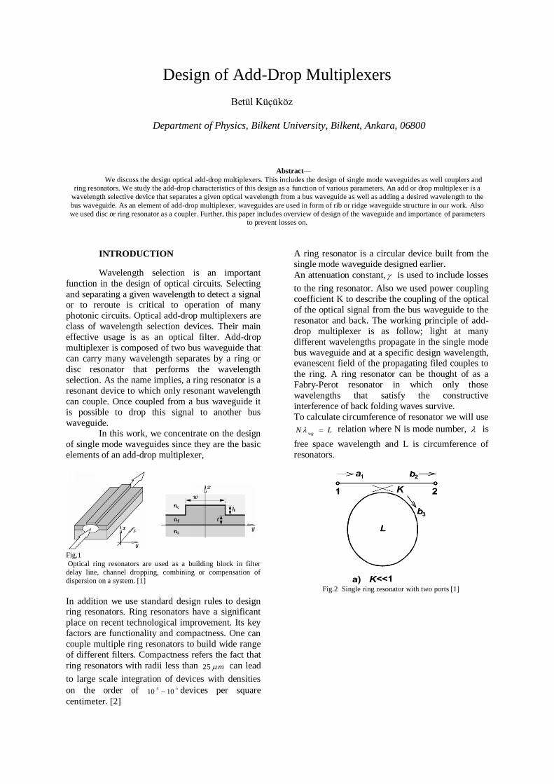
Fig.1
Optical ring resonators are used as a building block in filter
delay line, channel dropping, combining or compensation of
dispersion on a system. [1]
In addition we use standard design rules to design ring resonators. Ring resonators have a significant
place on recent technological improvement. Its key
factors are functionality and compactness. One can
couple multiple ring resonators to build wide range
of different filters. Compactness refers the fact that
ring resonators with radii less than m25 can lead
to large scale integration of devices with densities
on the order of 541010 devices per square
centimeter. [2]
A ring resonator is a circular device built from the single mode waveguide designed earlier.
An attenuation constant, is used to include losses
to the ring resonator. Also we used power coupling
coefficient K to describe the coupling of the optical
of the optical signal from the bus waveguide to the
resonator and back. The working principle of add-
drop multiplexer is as follow; light at many
different wavelengths propagate in the single mode
bus waveguide and at a specific design wavelength, evanescent field of the propagating filed couples to
the ring. A ring resonator can be thought of as a
Fabry-Perot resonator in which only those
wavelengths that satisfy the constructive
interference of back folding waves survive.
To calculate circumference of resonator we will use
LNwg
relation where N is mode number, is
free space wavelength and L is circumference of
resonators.
Fig.2 Single ring resonator with two ports [1]
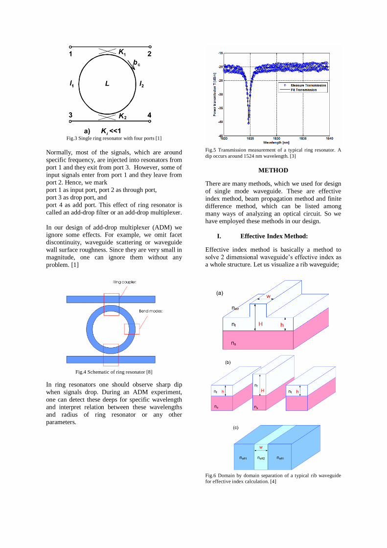
Fig.3 Single ring resonator with four ports [1]
Normally, most of the signals, which are around
specific frequency, are injected into resonators from
port 1 and they exit from port 3. However, some of
input signals enter from port 1 and they leave from
port 2. Hence, we mark
port 1 as input port, port 2 as through port,
port 3 as drop port, and
port 4 as add port. This effect of ring resonator is
called an add-drop filter or an add-drop multiplexer.
In our design of add-drop multiplexer (ADM) we ignore some effects. For example, we omit facet
discontinuity, waveguide scattering or waveguide
wall surface roughness. Since they are very small in
magnitude, one can ignore them without any
problem. [1]
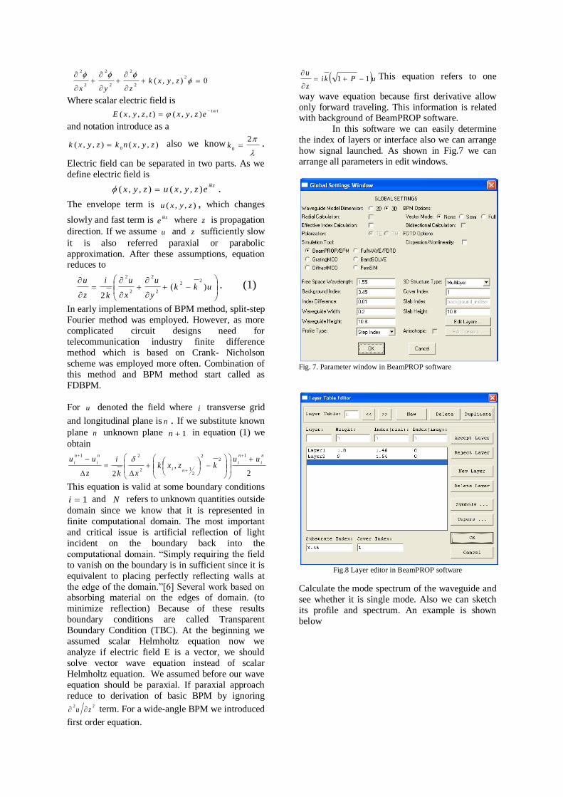
Fig.4 Schematic of ring resonator [8]
In ring resonators one should observe sharp dip
when signals drop. During an ADM experiment,
one can detect these deeps for specific wavelength
and interpret relation between these wavelengths
and radius of ring resonator or any other
parameters.
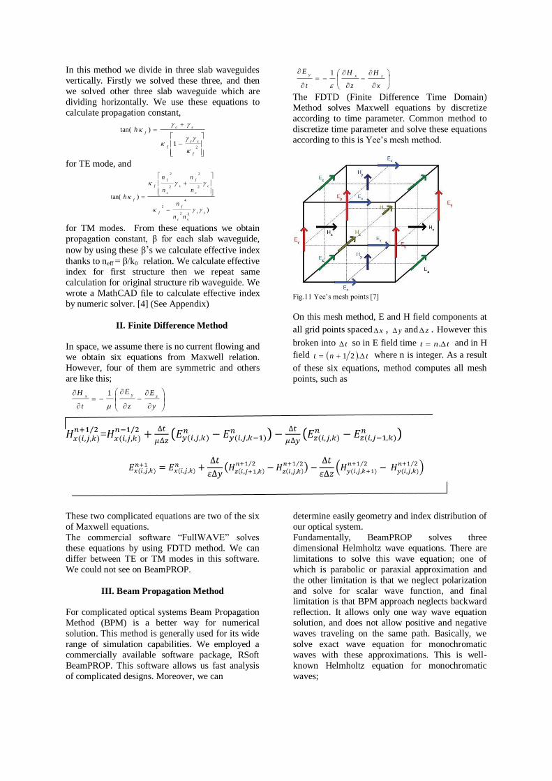
Fig.5 Transmission measurement of a typical ring resonator. A
dip occurs around 1524 nm wavelength. [3]
METHOD
There are many methods, which we used for design
of single mode waveguide. These are effective
index method, beam propagation method and finite
difference method, which can be listed among
many ways of analyzing an optical circuit. So we
have employed these methods in our design.
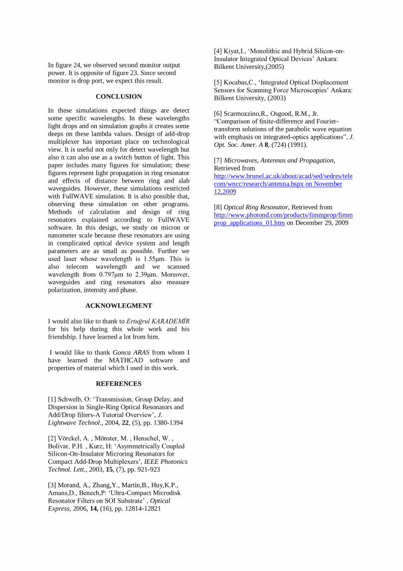
I. Effective Index Method:
Effective index method is basically a method to
solve 2 dimensional waveguide‟s effective index as a whole structure. Let us visualize a rib waveguide;
Fig.6 Domain by domain separation of a typical rib waveguide
for effective index calculation. [4]
In this method we divide in three slab waveguides
vertically. Firstly we solved these three, and then
we solved other three slab waveguide which are
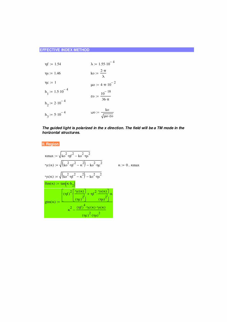
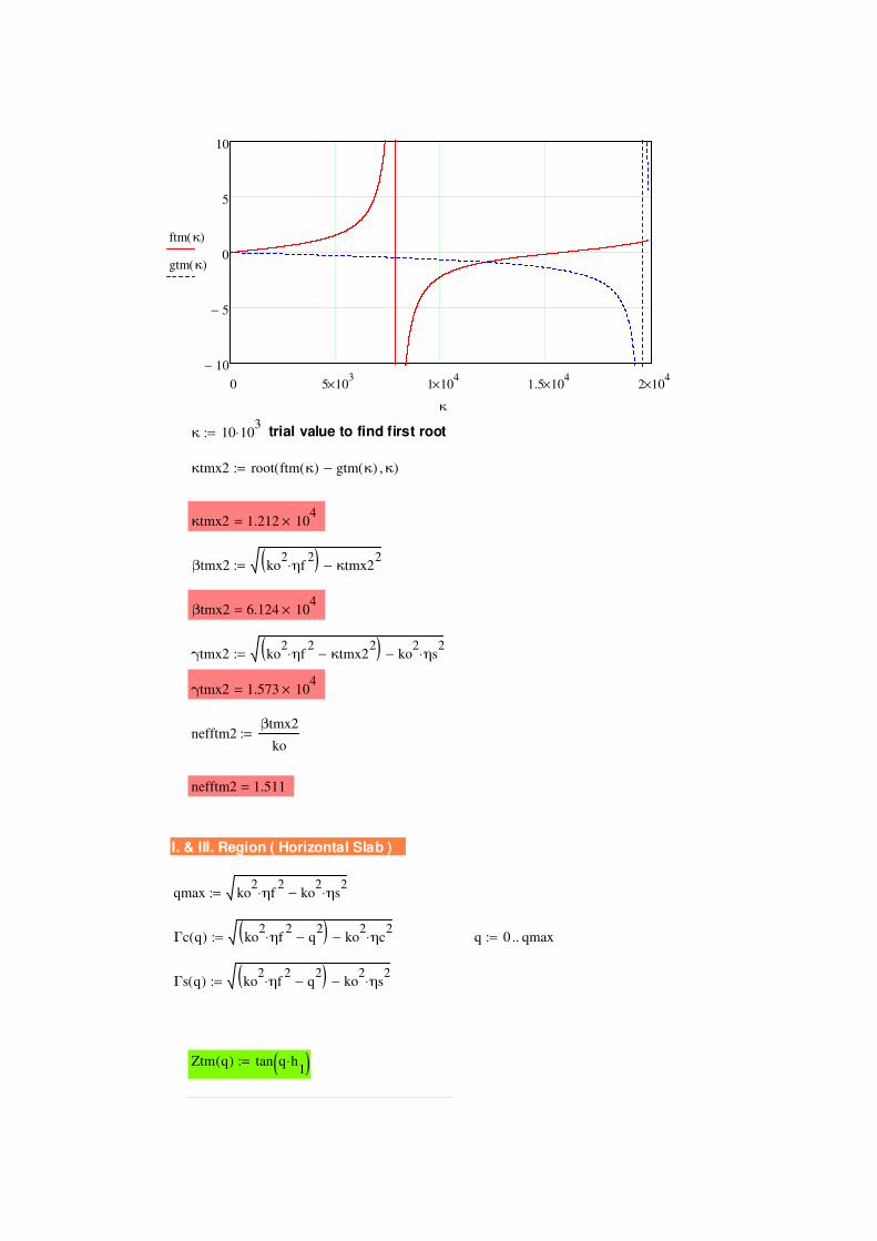
dividing horizontally. We use these equations to
calculate propagation constant,
21
)tan(
f
sc
f
sc
fh
for TE mode, and
)
)tan(
22
4
2
2
2
2
2
sc
sc
f
f
c
c
f
s
s
f
f
f
nn
n
n
n
n
n
h
for TM modes. From these equations we obtain
propagation constant, β for each slab waveguide,
now by using these β‟s we calculate effective index
thanks to neff = β/k0 relation. We calculate effective
index for first structure then we repeat same
calculation for original structure rib waveguide. We
wrote a MathCAD file to calculate effective index
by numeric solver. [4] (See Appendix)
II. Finite Difference Method
In space, we assume there is no current flowing and
we obtain six equations from Maxwell relation.
However, four of them are symmetric and others
are like this;
y
E
z
E
t
Hzyx
1
x
H
z
H
t
Ezxy
1
The FDTD (Finite Difference Time Domain)
Method solves Maxwell equations by discretize
according to time parameter. Common method to
discretize time parameter and solve these equations
according to this is Yee‟s mesh method.
Fig.11 Yee‟s mesh points [7]
On this mesh method, E and H field components at
all grid points spaced x , y and z . However this
broken into t so in E field time tnt . and in H
field tnt .21 where n is integer. As a result
of these six equations, method computes all mesh
points, such as
=
These two complicated equations are two of the six
of Maxwell equations.
The commercial software “FullWAVE” solves
these equations by using FDTD method. We can
differ between TE or TM modes in this software.
We could not see on BeamPROP.
III. Beam Propagation Method
For complicated optical systems Beam Propagation
Method (BPM) is a better way for numerical
solution. This method is generally used for its wide
range of simulation capabilities. We employed a
commercially available software package, RSoft
BeamPROP. This software allows us fast analysis
of complicated designs. Moreover, we can
determine easily geometry and index distribution of
our optical system.
Fundamentally, BeamPROP solves three
dimensional Helmholtz wave equations. There are
limitations to solve this wave equation; one of
which is parabolic or paraxial approximation and
the other limitation is that we neglect polarization
and solve for scalar wave function, and final limitation is that BPM approach neglects backward
reflection. It allows only one way wave equation
solution, and does not allow positive and negative
waves traveling on the same path. Basically, we
solve exact wave equation for monochromatic
waves with these approximations. This is well-
known Helmholtz equation for monochromatic
waves;
0),,(2
2
2
2
2
2
2
zyxk
zyx
Where scalar electric field is tt
ezyxtzyxE
),,(),,,(
and notation introduce as a
),,(),,(0
zyxnkzyxk also we know
20k .
Electric field can be separated in two parts. As we
define electric field is ikz
ezyxuzyx ),,(),,( .
The envelope term is ),,( zyxu , which changes
slowly and fast term is ikze where z is propagation
direction. If we assume u and z sufficiently slow
it is also referred paraxial or parabolic
approximation. After these assumptions, equation reduces to
ukk
y
u
x
u
k
i
z
u)(
2
22
2
2
2
2
. (1)
In early implementations of BPM method, split-step
Fourier method was employed. However, as more
complicated circuit designs need for
telecommunication industry finite difference
method which is based on Crank- Nicholson
scheme was employed more often. Combination of
this method and BPM method start called as
FDBPM.
For u denoted the field where i transverse grid
and longitudinal plane is n . If we substitute known
plane n unknown plane 1n in equation (1) we
obtain
2,
2
12
2
212
21 n
i
n
i
ni
n
i
n
iuu
kzxkxk
i
z
uu
This equation is valid at some boundary conditions
1i and N refers to unknown quantities outside
domain since we know that it is represented in
finite computational domain. The most important
and critical issue is artificial reflection of light
incident on the boundary back into the
computational domain. “Simply requiring the field
to vanish on the boundary is in sufficient since it is
equivalent to placing perfectly reflecting walls at
the edge of the domain.”[6] Several work based on absorbing material on the edges of domain. (to
minimize reflection) Because of these results
boundary conditions are called Transparent
Boundary Condition (TBC). At the beginning we
assumed scalar Helmholtz equation now we
analyze if electric field E is a vector, we should
solve vector wave equation instead of scalar
Helmholtz equation. We assumed before our wave
equation should be paraxial. If paraxial approach
reduce to derivation of basic BPM by ignoring 22
zu term. For a wide-angle BPM we introduced
first order equation.
uPkiz
u11
This equation refers to one
way wave equation because first derivative allow
only forward traveling. This information is related with background of BeamPROP software.
In this software we can easily determine
the index of layers or interface also we can arrange
how signal launched. As shown in Fig.7 we can
arrange all parameters in edit windows.
Fig. 7. Parameter window in BeamPROP software
Fig.8 Layer editor in BeamPROP software
Calculate the mode spectrum of the waveguide and
see whether it is single mode. Also we can sketch
its profile and spectrum. An example is shown
below
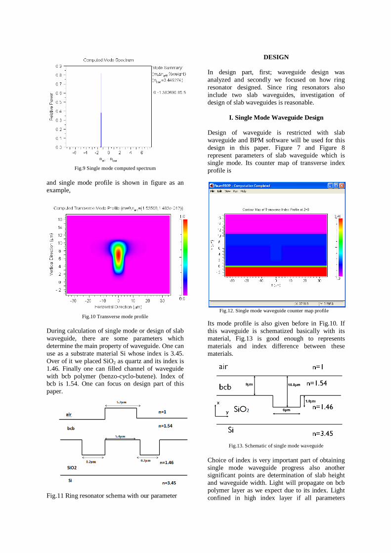
Fig.9 Single mode computed spectrum
and single mode profile is shown in figure as an
example,
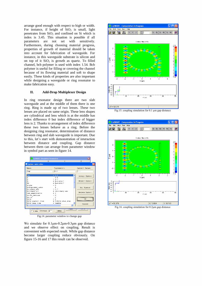
Fig.10 Transverse mode profile
During calculation of single mode or design of slab
waveguide, there are some parameters which
determine the main property of waveguide. One can
use as a substrate material Si whose index is 3.45.
Over of it we placed SiO2 as quartz and its index is
1.46. Finally one can filled channel of waveguide
with bcb polymer (benzo-cyclo-butene). Index of bcb is 1.54. One can focus on design part of this
paper.
Fig.11 Ring resonator schema with our parameter
DESIGN
In design part, first; waveguide design was
analyzed and secondly we focused on how ring
resonator designed. Since ring resonators also
include two slab waveguides, investigation of
design of slab waveguides is reasonable.
I. Single Mode Waveguide Design
Design of waveguide is restricted with slab
waveguide and BPM software will be used for this
design in this paper. Figure 7 and Figure 8
represent parameters of slab waveguide which is
single mode. Its counter map of transverse index
profile is
Fig.12. Single mode waveguide counter map profile
Its mode profile is also given before in Fig.10. If
this waveguide is schematized basically with its
material, Fig.13 is good enough to represents
materials and index difference between these
materials.
Fig.13. Schematic of single mode waveguide
Choice of index is very important part of obtaining
single mode waveguide progress also another significant points are determination of slab height
and waveguide width. Light will propagate on bcb
polymer layer as we expect due to its index. Light
confined in high index layer if all parameters
arrange good enough with respect to high or width.
For instance, if height of SiO2 is small, light
penetrates from SiO2 and confined on Si which is
index is 3.45. This situation is possible if all
parameters are not set with sensitively.
Furthermore, during choosing material progress,
properties of growth of material should be taken
into account for fabrication of waveguide. For
instance, in this waveguide substrate is silicon and on top of it SiO2 is growth as quartz. To filled
channel, bcb polymer is used with index 1.54. Bcb
polymer is useful for filling or covering the channel
because of its flowing material and soft to shape
easily. These kinds of properties are also important
while designing a waveguide or ring resonator to
make fabrication easy.
II. Add-Drop Multiplexer Design
In ring resonator design there are two slab waveguide and at the middle of them there is one
ring. Ring is made up of two lenses. These two
lenses are placed on same origin. These lens shapes
are cylindrical and lens which is at the middle has
index difference 0 but index difference of bigger
lens is 2. Thanks to arrangement of index difference
these two lenses behave as a ring. Before the
designing ring resonator, determination of distance
between ring and slab waveguide is important. Due
to this, let‟s start with demonstration of interaction
between distance and coupling. Gap distance between them can arrange from parameter window
in symbol part as seen in figure 14.
Fig.14. parameter window to change gap
We simulate for 0.1μm-0.2μm-0.3μm gap distance
and we observe effect on coupling. Result is
convenient with expected result. While gap distance
become larger coupling reduce obviously. On
figure 15-16 and 17 this result can be observed.
Fig.15. coupling simulation for 0.1 μm gap distance
Fig.16. coupling simulation for 0.2μm gap distance
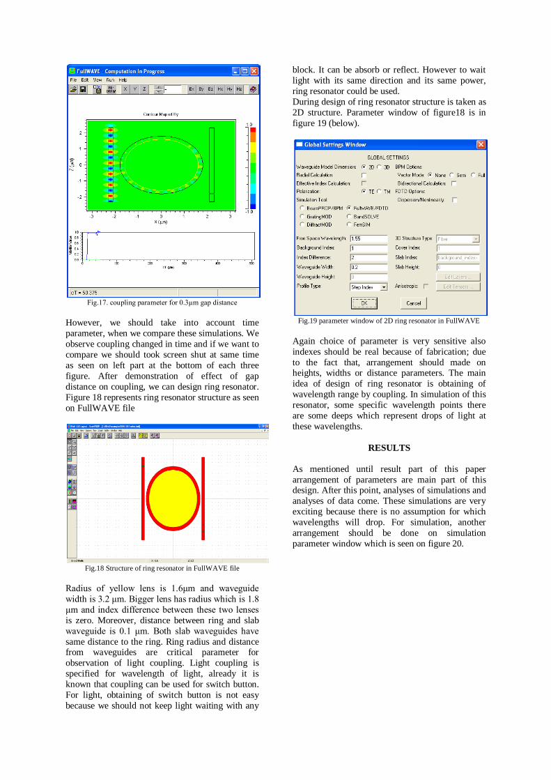
Fig.17. coupling parameter for 0.3μm gap distance
However, we should take into account time
parameter, when we compare these simulations. We
observe coupling changed in time and if we want to
compare we should took screen shut at same time
as seen on left part at the bottom of each three
figure. After demonstration of effect of gap
distance on coupling, we can design ring resonator.
Figure 18 represents ring resonator structure as seen
on FullWAVE file
Fig.18 Structure of ring resonator in FullWAVE file
Radius of yellow lens is 1.6μm and waveguide
width is 3.2 μm. Bigger lens has radius which is 1.8
μm and index difference between these two lenses
is zero. Moreover, distance between ring and slab
waveguide is 0.1 μm. Both slab waveguides have
same distance to the ring. Ring radius and distance from waveguides are critical parameter for
observation of light coupling. Light coupling is
specified for wavelength of light, already it is
known that coupling can be used for switch button.
For light, obtaining of switch button is not easy
because we should not keep light waiting with any
block. It can be absorb or reflect. However to wait
light with its same direction and its same power,
ring resonator could be used.
During design of ring resonator structure is taken as
2D structure. Parameter window of figure18 is in
figure 19 (below).
Fig.19 parameter window of 2D ring resonator in FullWAVE
Again choice of parameter is very sensitive also
indexes should be real because of fabrication; due
to the fact that, arrangement should made on heights, widths or distance parameters. The main
idea of design of ring resonator is obtaining of
wavelength range by coupling. In simulation of this
resonator, some specific wavelength points there
are some deeps which represent drops of light at
these wavelengths.
RESULTS
As mentioned until result part of this paper
arrangement of parameters are main part of this design. After this point, analyses of simulations and
analyses of data come. These simulations are very
exciting because there is no assumption for which
wavelengths will drop. For simulation, another
arrangement should be done on simulation
parameter window which is seen on figure 20.
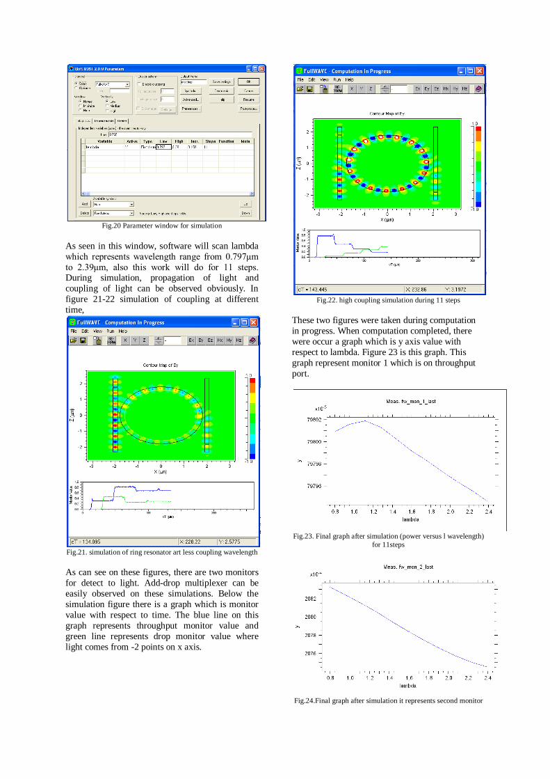
Fig.20 Parameter window for simulation
As seen in this window, software will scan lambda
which represents wavelength range from 0.797μm
to 2.39μm, also this work will do for 11 steps. During simulation, propagation of light and
coupling of light can be observed obviously. In
figure 21-22 simulation of coupling at different
time,
Fig.21. simulation of ring resonator art less coupling wavelength
As can see on these figures, there are two monitors
for detect to light. Add-drop multiplexer can be
easily observed on these simulations. Below the
simulation figure there is a graph which is monitor
value with respect to time. The blue line on this
graph represents throughput monitor value and
green line represents drop monitor value where
light comes from -2 points on x axis.
Fig.22. high coupling simulation during 11 steps
These two figures were taken during computation
in progress. When computation completed, there
were occur a graph which is y axis value with
respect to lambda. Figure 23 is this graph. This
graph represent monitor 1 which is on throughput
port.
Fig.23. Final graph after simulation (power versus l wavelength)
for 11steps
Fig.24.Final graph after simulation it represents second monitor
In figure 24, we observed second monitor output
power. It is opposite of figure 23. Since second
monitor is drop port, we expect this result.
CONCLUSION
In these simulations expected things are detect
some specific wavelengths. In these wavelengths
light drops and on simulation graphs it creates some
deeps on these lambda values. Design of add-drop
multiplexer has important place on technological
view. It is useful not only for detect wavelength but
also it can also use as a switch button of light. This
paper includes many figures for simulation; these
figures represent light propagation in ring resonator
and effects of distance between ring and slab waveguides. However, these simulations restricted
with FullWAVE simulation. It is also possible that,
observing these simulation on other programs.
Methods of calculation and design of ring
resonators explained according to FullWAVE
software. In this design, we study on micron or
nanometer scale because these resonators are using
in complicated optical device system and length
parameters are as small as possible. Further we
used laser whose wavelength is 1.55μm. This is
also telecom wavelength and we scanned
wavelength from 0.797μm to 2.39μm. Moreover, waveguides and ring resonators also measure
polarization, intensity and phase.
ACKNOWLEGMENT
I would also like to thank to Ertuğrul KARADEMİR
for his help during this whole work and his
friendship. I have learned a lot from him.
I would like to thank Gonca ARAS from whom I
have learned the MATHCAD software and properties of material which I used in this work.
REFERENCES
[1] Schwelb, O: „Transmission, Group Delay, and
Dispersion in Single-Ring Optical Resonators and
Add/Drop filters-A Tutorial Overview‟, J.
Lightwave Technol., 2004, 22, (5), pp. 1380-1394
[2] Vörckel, A. , Mönster, M. , Henschel, W. ,
Bolivar, P.H. , Kurz, H: „Asymmetrically Coupled Silicon-On-Insulator Microring Resonators for
Compact Add-Drop Multiplexers‟, IEEE Photonics
Technol. Lett., 2003, 15, (7), pp. 921-923
[3] Morand, A., Zhang,Y., Martin,B., Huy,K.P.,
Amans,D., Benech,P: „Ultra-Compact Microdisk
Resonator Filters on SOI Substrate‟ , Optical
Express, 2006, 14, (16), pp. 12814-12821
[4] Kiyat,I., „Monolithic and Hybrid Silicon-on-
Insulator Integrated Optical Devices‟ Ankara:
Bilkent University,(2005)
[5] Kocabas,C., „Integrated Optical Displacement
Sensors for Scanning Force Microscopies‟ Ankara:
Bilkent University, (2003)
[6] Scarmozzino,R., Osgood, R.M., Jr. “Comparison of finite-difference and Fourier-
transform solutions of the parabolic wave equation
with emphasis on integrated-optics applications”, J.
Opt. Soc. Amer. A 8, (724) (1991).
[7] Microwaves, Antennas and Propagation,
Retrieved from
http://www.brunel.ac.uk/about/acad/sed/sedres/tele
com/wncc/research/antenna.bspx on November
12,2009
[8] Optical Ring Resonator, Retrieved from
http://www.photond.com/products/fimmprop/fimm
prop_applications_01.htm on December 29, 2009

APPENDIX
EFFECTIVE INDEX METHOD
ηf 1.54:= λ 1.55 104−
⋅:=
ηs 1.46:= ko2 π⋅
λ:=
ηc 1:=μo 4 π⋅ 10
2−⋅:=
h1
1.5 104−
⋅:=
εo10
18−
36 π⋅:=
h2
2 104−
⋅:=
ωoko
μo εo⋅:=
h3
5 104−
⋅:=
The guided light is polarized in the x direction. The field will be a TM mode in the
horizontal structures.
II. Region
κmax ko2ηf
2⋅ ko
2ηs
2⋅−:=
γc κ( ) ko2ηf
2⋅ κ
2−( ) ko
2ηc
2⋅−:= κ 0 κmax..:=
γs κ( ) ko2ηf
2⋅ κ
2−( ) ko
2ηs
2⋅−:=
ftm κ( ) tan κ h2
⋅( ):=
gtm κ( )
ηf( )2 γc κ( )
ηc( )2
⋅ ηf2 γs κ( )
ηs( )2
⋅+
κ⋅
κ2 ηf( )
4γc κ( )⋅ γs κ( )⋅
ηc( )2ηs( )
2⋅
−
:=
0 5 103
× 1 104
× 1.5 104
× 2 104
×
10−
5−
0
5
10
ftm κ( )
gtm κ( )
κ
κ 10 103
⋅:= trial value to find first root
κtmx2 root ftm κ( ) gtm κ( )− κ, ( ):=
κtmx2 1.212 104
×=
βtmx2 ko2ηf
2⋅( ) κtmx2
2−:=
βtmx2 6.124 104
×=
γtmx2 ko2ηf
2⋅ κtmx2
2−( ) ko
2ηs
2⋅−:=
γtmx2 1.573 104
×=
nefftm2βtmx2
ko:=
nefftm2 1.511=
I. & III. Region ( Horizontal Slab )
qmax ko2ηf
2⋅ ko
2ηs
2⋅−:=
Γc q( ) ko2ηf
2⋅ q
2−( ) ko
2ηc
2⋅−:= q 0 qmax..:=
Γs q( ) ko2ηf
2⋅ q
2−( ) ko
2ηs
2⋅−:=
Ztm q( ) tan q h1
⋅( ):=
Γtm q( )
ηf( )2 Γc q( )
ηc( )2
⋅ ηf2 Γs q( )
ηs( )2
⋅+
q⋅
q2 ηf( )
4Γc q( )⋅ Γs q( )⋅
ηc( )2ηs( )
2⋅
−
:=
0 5 103
× 1 104
× 1.5 104
× 2 104
×
10−
5−
0
5
10
Ztm q( )
Γtm q( )
q
q 1.5 104
⋅:= trial value to find first root
qtm1 root Ztm q( ) Γtm q( )− q, ( ):=
qtm1 1.478 104
×=
βtm1 ko2ηf
2⋅ qtm1( )
2−:=
βtm1 6.065 104
×=
nefftm1βtm1
ko:=
nefftm1 1.496=
For TE( Vertical Structure ),
Umax ko2
nefftm22
⋅ ko2
nefftm12
⋅−:=
( )
γyte u( ) ko2
nefftm22
⋅ u2
−( ) ko2
nefftm12
⋅−:= u 0 Umax..:=
Umax 8.462 103
×=r u( ) tan
u h3
⋅
2
:=
b u( )γyte u( )
u:=
0 2 103
× 4 103
× 6 103
× 8 103
× 1 104
×
10−
5−
0
5
10
r u( )
b u( )
u
u 2 103
⋅:= trial value to find first root
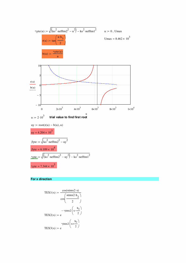
uy root r u( ) b u( )− u, ( ):=
uy 4.204 103
×=
βyte ko2
nefftm22
⋅ uy2
−:=
βyte 6.109 104
×=
γyte ko2
nefftm22
⋅ uy2
−( ) ko2
nefftm12
⋅−:=
γyte 7.344 103
×=
For x direction
TEX1 x( )cos κtmx2 x⋅( )
cos
κtmx2 h2
⋅
2
:=
TEX2 x( ) e
γtmx2− xh2
2−
⋅
:=
TEX3 x( ) e
γtmx2 xh2
2+
⋅
:=
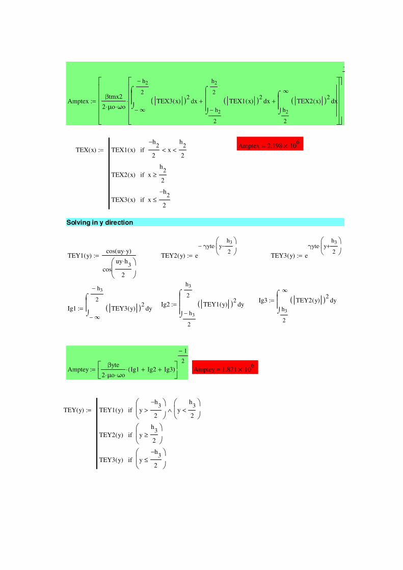
Amptexβtmx2
2 μo⋅ ωo⋅∞−
h2−
2
xTEX3 x( )( )2
⌠⌡
d
h2−
2
h2
2
xTEX1 x( )( )2
⌠⌡
d+
h2
2
∞
xTEX2 x( )( )2⌠
⌡
d+
⋅
−
:=
Amptex 2.198 106
×=TEX x( ) TEX1 x( )
h2
−
2x<
h2
2<if
TEX2 x( ) x
h2
2≥if
TEX3 x( ) x
h2
−
2≤if
:=
Solving in y direction
TEY1 y( )cos uy y⋅( )
cos
uy h3
⋅
2
:= TEY2 y( ) e
γyte− yh3
2−
⋅
:= TEY3 y( ) e
γyte yh3
2+
⋅
:=
Ig3
h3
2
∞
yTEY2 y( )( )2⌠
⌡
d:=Ig2
h3−
2
h3
2
yTEY1 y( )( )2
⌠⌡
d:=Ig1
∞−
h3−
2
yTEY3 y( )( )2
⌠⌡
d:=
Ampteyβyte
2 μo⋅ ωo⋅Ig1 Ig2+ Ig3+( )⋅
1−
2
:= Amptey 1.871 106
×=
TEY y( ) TEY1 y( ) y
h3
−
2>
y
h3
2<
∧if
TEY2 y( ) y
h3
2≥
if
TEY3 y( ) y
h3
−
2≤
if
:=
1− 103−
× 5− 104−
× 0 5 104−
× 1 103−
×
0
2 106
×
4 106
×
6 106
×
8 106
×
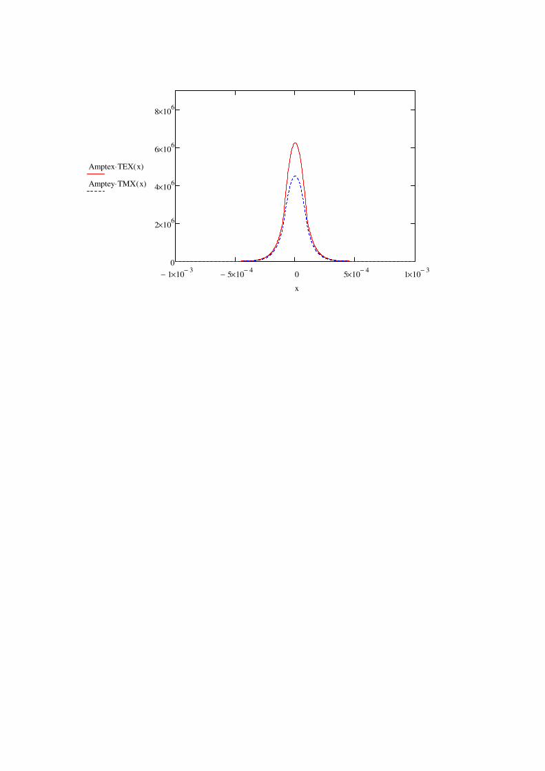
Amptex TEX x( )⋅
Amptey TMX x( )⋅
x
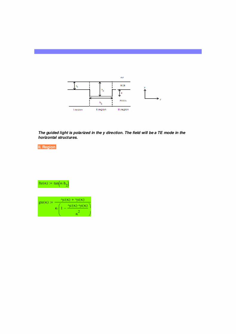
The guided light is polarized in the y direction. The field will be a TE mode in the
horizontal structures.
II. Region
fte κ( ) tan κ h2
⋅( ):=
gte κ( )γc κ( ) γs κ( )+
κ 1γc κ( ) γs κ( )⋅
κ2
−
⋅
:=
0 5 103
× 1 104
× 1.5 104
× 2 104
×
10−
5−
0
5
10
fte κ( )
gte κ( )
κ
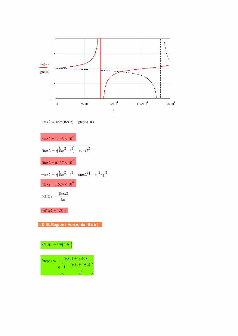
κtex2 root fte κ( ) gte κ( )− κ, ( ):=
κtex2 1.143 104
×=
βtex2 ko2ηf
2⋅( ) κtex2
2−:=
βtex2 6.137 104
×=
γtex2 ko2ηf
2⋅ κtex2
2−( ) ko
2ηs
2⋅−:=
γtex2 1.624 104
×=
neffte2βtex2
ko:=
neffte2 1.514=
I. & III. Region ( Horizontal Slab )
Zte q( ) tan q h1
⋅( ):=
Rte q( )γc q( ) γs q( )+
q 1γc q( ) γs q( )⋅
q2
−
⋅
:=
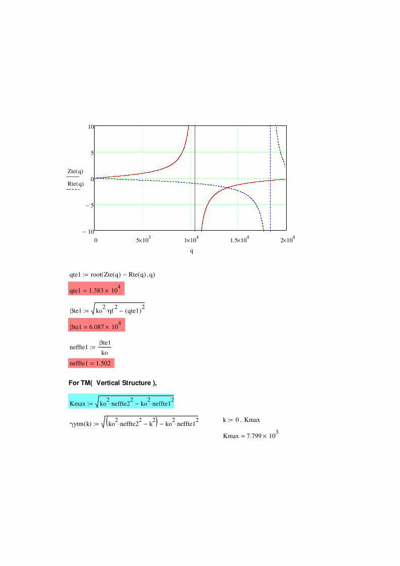
0 5 103
× 1 104
× 1.5 104
× 2 104
×
10−
5−
0
5
10
Zte q( )
Rte q( )
q
qte1 root Zte q( ) Rte q( )− q, ( ):=
qte1 1.383 104
×=
βte1 ko2ηf
2⋅ qte1( )
2−:=
βte1 6.087 104
×=
neffte1βte1
ko:=
neffte1 1.502=
For TM( Vertical Structure ),
Kmax ko2
neffte22
⋅ ko2
neffte12
⋅−:=
k 0 Kmax..:=γytm k( ) ko
2neffte2
2⋅ k
2−( ) ko
2neffte1
2⋅−:=
Kmax 7.799 103
×=
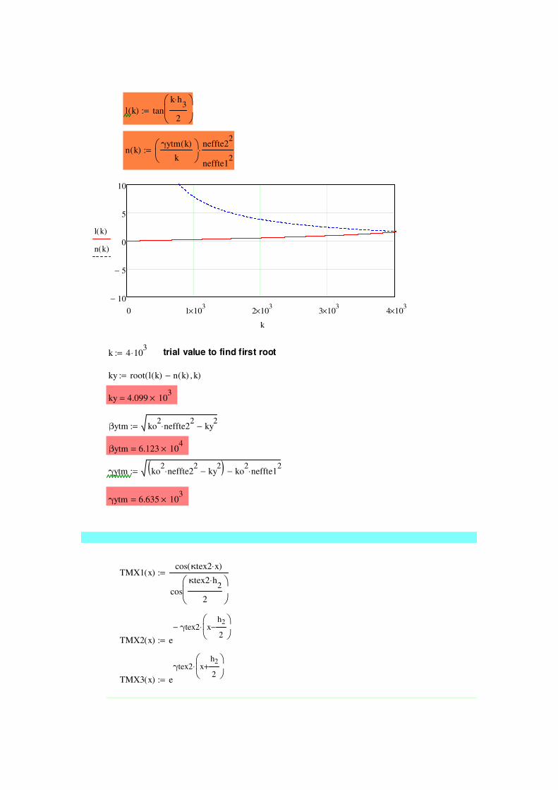
l k( ) tan
k h3
⋅
2
:=
n k( )γytm k( )
k
neffte22
neffte12
⋅:=
0 1 103
× 2 103
× 3 103
× 4 103
×
10−
5−
0
5
10
l k( )
n k( )
k
k 4 103
⋅:= trial value to find first root
ky root l k( ) n k( )− k, ( ):=
ky 4.099 103
×=
βytm ko2
neffte22
⋅ ky2
−:=
βytm 6.123 104
×=
γytm ko2
neffte22
⋅ ky2
−( ) ko2
neffte12
⋅−:=
γytm 6.635 103
×=
TMX1 x( )cos κtex2 x⋅( )
cos
κtex2 h2
⋅
2
:=
TMX2 x( ) e
γtex2− xh2
2−
⋅
:=
TMX3 x( ) e
γtex2 xh2
2+
⋅
:=
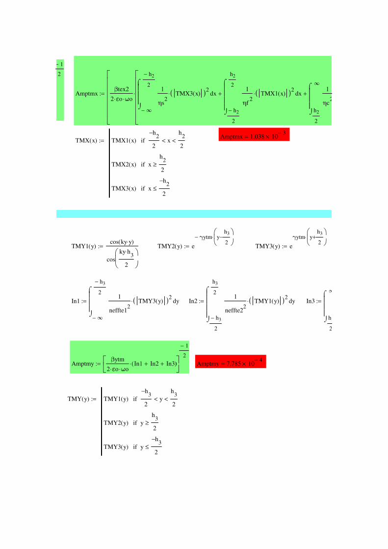
Amptmxβtex2
2 εo⋅ ωo⋅
∞−
h2−
2
x1
ηs2
TMX3 x( )( )2
⋅
⌠⌡
d
h2−
2
h2
2
x1
ηf2
TMX1 x( )( )2
⋅
⌠⌡
d+
h2
2
∞1
ηc2
⌠⌡
+
⋅
:=
1−
2
Amptmx 1.038 103−
×=TMX x( ) TMX1 x( )
h2
−
2x<
h2
2<if
TMX2 x( ) x
h2
2≥if
TMX3 x( ) x
h2
−
2≤if
:=
TMY1 y( )cos ky y⋅( )
cos
ky h3
⋅
2
:= TMY2 y( ) e
γytm− yh3
2−
⋅
:= TMY3 y( ) e
γytm yh3
2+
⋅
:=
In1
∞−
h3−
2
y1
neffte12
TMY3 y( )( )2
⋅
⌠⌡
d:= In2
h3−
2
h3
2
y1
neffte22
TMY1 y( )( )2
⋅
⌠⌡
d:= In3
h3
2
∞⌠⌡
:=
Amptmyβytm
2 εo⋅ ωo⋅In1 In2+ In3+( )⋅
1−
2
:= Amptmy 7.785 104−
×=
TMY y( ) TMY1 y( )
h3
−
2y<
h3
2<if
TMY2 y( ) y
h3
2≥if
TMY3 y( ) y
h3
−
2≤if
:=
0.01− 5− 103−
× 0 5 103−
× 0.01
0
5 104−
×
1 103−
×
1.5 103−
×
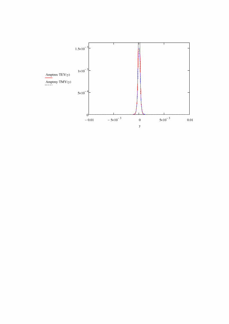
Amptmx TEY y( )⋅
Amptmy TMY y( )⋅
y


x2
TMX2 x( )( )2
⋅ d
1−
2
3
2
∞
y1
neffte12
TMY2 y( )( )2
⋅ d


![Encoders, Decoders,Multiplexers and Demultiplexers [Compatibility Mode]](https://img.pdfslide.us/doc/110x75/577cc9e01a28aba711a4d3c2/encoders-decodersmultiplexers-and-demultiplexers-compatibility-mode.jpg)