Embed Size (px)
Citation preview
8/9/2019 Design of a Wide Band RF Amplifier using Scattering Parameters
http://slidepdf.com/reader/full/design-of-a-wide-band-rf-amplifier-using-scattering-parameters 1/4
International Journal of Computer Applications (0975 – 8887)
Volume 66 – No.11, March 2013
1
Design of a Wide Band RF Amplifier using
Scattering Parameters
Sami Mahersi, Mohamed Dhieb, Hamadi Ghariani and Mounir SametLaboratory of Electronics and Information Technologies
University of SfaxSfax, Tunisia
ABSTRACT
This paper presents a new concept of a wide band RF
amplifier using scattering parameters that is often used in theradio frequency communication system. This amplifieroperates from 80MHz to 1.1GHz frequency and it is based onBFG65 NPN transistor that has a high transition frequency of
7.5GHz [1]. The simulation results show good performances.The power gain S21 is varied between 10 and 14.34 dB. Forthe input reflection coefficient S
11is changed between -29.3
and -17.61 dB. Regarding the output reflection coefficient S22
is varied between -19.78 and -10.36 dB. For the reversetransmission S12 is changed between -23.23 and -24.65 dB.Regarding the noise figure NF is varied between 3.6 and
3.9 dB. For the 1 dB compression point is changed between-13.94 and -8.24 dBm.
Keywords
Wide band RF amplifier, Input matching, Output matching,RF communication system.
1. INTRODUCTIONIn the input of the radio frequency reception chain, the RFsignal is mitigated because its power decreases during
emission stage. For this reason, The RF amplifier is verysignificant. In addition, without this part the receiptinformation can not be recognized. On the other hand, the power gain of this amplifier must be sufficient to predict theuseful information.
The narrow band and the wide band microwaves amplifiers
are very used in the communication and detection systems(spatial telecommunication, radio communication, radardetection, control system, …) [2]. The matching networks of
these amplifiers are designed by means of localized elements
(inductances and capacitors) or to basis of distributedelements (transmission lines) or a combination of the two [3],[4], [5], [6]. The use of the matching networks by means ofthe localized elements or distributed elements depend on the
operation frequency. Indeed, for the frequencies lower than6GHz the localized elements are mainly used, and for themore high frequencies the distributed elements are extensivelyused, this for the economic and technological constraints [5].
In this paper, we present a novel design of a wide band RFamplifier using the transistor BFG65 that of type BJT (Bipolar
Junction Transistor). Also, it is a UHF/microwave transistor.This amplifier uses two RC matching networks to match theinput and output at 50 Ohm. In what follows, we present the design of a wide band RF
amplifier using scattering parameters, where we study the RFamplifier in the DC mode and then we simulate the amplifierusing ADS (Advanced Design System) simulator. Also, we
show the performances of the RF wide band amplifier.Finally, we conclude.
2. DESIGN OF A WIDE BAND RF
AMPLIFIER USING SCATTERING
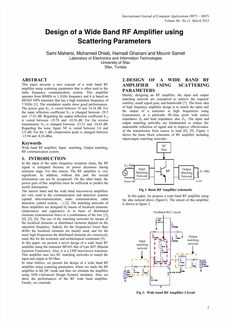
PARAMETERSMainly, designing an RF amplifier, the input and output
matching network are considered to achieve the requiredstability, small signal gain, and bandwidth [7]. The basic ideaof high frequency amplifier design is to match the input and
the output of a transistor at high frequencies using
S-parameters at a particular DC-bias point with sourceimpedance Z0 and load impedance also Z0. The input andoutput matching networks are fundamental to reduce theundesirable reflection of signal and to improve effectivenessof the transmission from source to load [8], [9]. Figure 1
shows the basic block schematic of RF amplifier including
input/output matching networks.
Fig 1: Basic RF Amplifier schematic
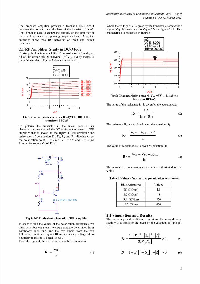
In this paper, we propose a wide band RF amplifier using
the idea noticed above (figure1). The circuit of this amplifieris shown in figure 2.
Fig 2: Wide band RF Amplifier Circuit
Inputmatching network
Outputmatching network
Feedback RLC circuit
SP
Output
Matching
Network
Z0=50Ω
Input
Matching Network
Z0=50Ω
Source RF
DC
Bias
Load
8/9/2019 Design of a Wide Band RF Amplifier using Scattering Parameters
http://slidepdf.com/reader/full/design-of-a-wide-band-rf-amplifier-using-scattering-parameters 2/4
International Journal of Computer Applications (0975 – 8887)
Volume 66 – No.11, March 2013
2
The proposed amplifier presents a feedback RLC circuit
between the collector and the base of the transistor BFG65.This circuit is used to ensure the stability of the amplifier in
the low frequencies of operating frequency band. Also, theamplifier shows two RC networks of input and outputmatching.
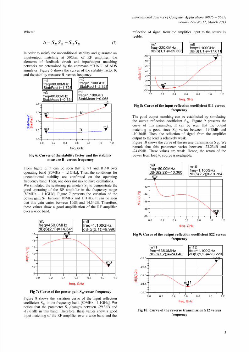
2.1
RF Amplifier Study in DC-ModeTo study the functioning of BFG65 transistor in DC mode, we
raised the characteristics network IC=f(VCE, IB) by means of
the ADS simulator. Figure 3 shows this network.
Fig 3: Characteristics network IC=f(VCE, IB) of the
transistor BFG65
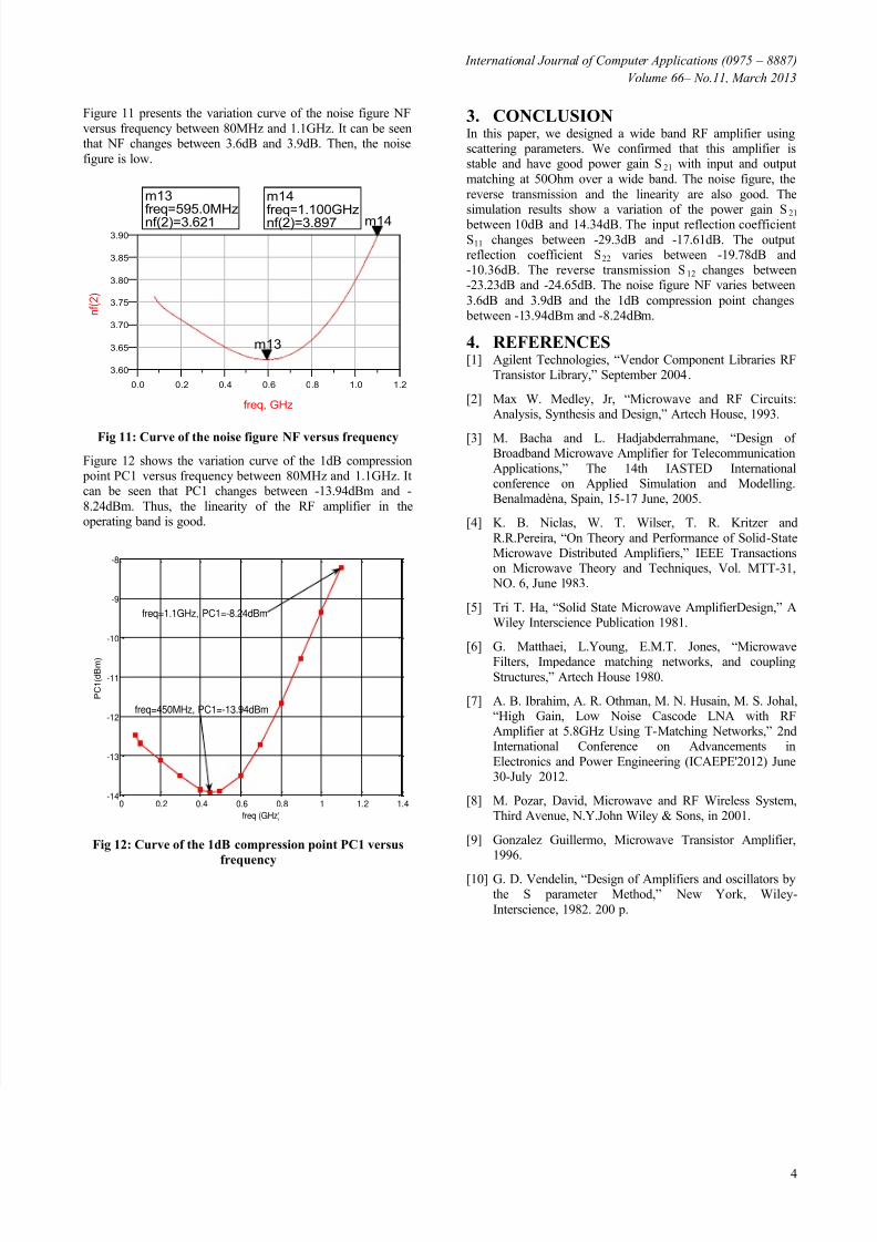
To polarize the transistor in the linear zone of itscharacteristic, we adopted the DC equivalent schematic of RFamplifier that is shown in the figure 4. We determine theresistances of polarization R 1, R 2, R 4 and R 5 allowing to get
the polarization point; IC = 7 mA, VCE = 3 V and IB = 60 µAfrom a bias source Vdc of 12 V.
Fig 4: DC Equivalent schematic of RF Amplifier
In order to find the values of the polarization resistances, wemust have four equations; two equations are determined fromKirchhoff's loop rule, and the two others from the twofollowing conditions: IB1 = 9 IB and we want a voltage fall to boundary-marks of R 5 equals to 3.5V.
From the figure 4, the resistance R 1 can be expressed as:
B1
BE
1
I
VR (1)
Where the voltage VBE is given by the transistor Characteristic
VBE =f(VCE, IB) associated to VCE = 3 V and IB = 60 µA. Thischaracteristic is presented in figure 5.
Fig 5: Characteristics network VBE =f(VCE, IB) of the
transistor BFG65
The value of the resistance R 5 is given by the equation (2):
BC
5
10II
3.5R
(2)
The resistance R 4 is calculated using the equation (3):
C
CECC
4
I
3.5VVR
(3)
The value of resistance R 2 is given by equation (4):
B2
C4BECE
2
I
IR VVR
(4)
The normalised polarization resistances are illustrated in thetable 1.
Table 1. Values of normalized polarization resistances
Bias resistances Values
R1 (KOhm) 1.5
R2 (KOhm) 13
R4 (KOhm) 820
R5 (Ohm) 470
2.2 Simulation and ResultsThe necessary and sufficient conditions for unconditionalstability of a transistor are given by the equations (5) and (6)
[10]:
1..2
1
2112
22
22
2
11
S S
S S K (5)
01 22
22
2
111 S S B (6)
1 2 3 40 5
0
5
10
-5
15
IBB=2.000E-5
IBB=3.000E-5
IBB=4.000E-5IBB=5.000E-5
IBB=6.000E-5
IBB=7.000E-5IBB=8.000E-5
IBB=9.000E-5IBB=1.000E-4
VCE
I C . i , m A
m1
m1
VCE=
IC.i=0.007
IBB=0.000060
3.000
1 2 3 40 5
700
750
800
650
850
VCE
V B E , m V
m2
m2
VCE=
VBE=0.794
IBB=0.000060
3.000
8/9/2019 Design of a Wide Band RF Amplifier using Scattering Parameters
http://slidepdf.com/reader/full/design-of-a-wide-band-rf-amplifier-using-scattering-parameters 3/4
International Journal of Computer Applications (0975 – 8887)
Volume 66 – No.11, March 2013
3
Where:
21121122 S S S S (7)
In order to satisfy the unconditional stability and guarantee an
input/output matching at 50Ohm of RF amplifier, the
elements of feedback circuit and input/output matchingnetworks are determined by the command “TUNE” of ADS
simulator. Figure 6 shows the curves of the stability factor K
and the stability measure B1 versus frequency.
Fig 6: Curves of the stability factor and the stability
measure B1 versus frequency
From figure 6, it can be seen that K >1 and B1>0 overoperating band [80MHz – 1.1GHz]. Thus, the conditions for
unconditional stability are confirmed on the operating
frequency band. Then, one does not risk to have oscillations.
We simulated the scattering parameters Sij to demonstrate thegood operating of the RF amplifier in the frequency range[80MHz – 1.1GHz]. Figure 7 presents the variation of the
power gain S21 between 80MHz and 1.1GHz. It can be seenthat this gain varies between 10dB and 14.34dB. Therefore,
these values show a good amplification of the RF amplifierover a wide band.
Fig 7: Curve of the power gain S21versus frequency
Figure 8 shows the variation curve of the input reflectioncoefficient S11 in the frequency band [80MHz - 1.1GHz]. We
notice that the parameter S11changes between -29.3dB and-17.61dB in this band. Therefore, these values show a good
input matching of the RF amplifier over a wide band and the
reflection of signal from the amplifier input to the source is
feeble.
Fig 8: Curve of the input reflection coefficient S11 versus
frequency
The good output matching can be established by simulatingthe output reflection coefficient S22. Figure 9 presents the
curve of this parameter. It can be seen that the output
matching is good since S22 varies between -19.78dB and-10.36dB. Then, the reflection of signal from the amplifieroutput to the load is relatively weak.Figure 10 shows the curve of the reverse transmission S12. We
remark that this parameter varies between -23.23dB and-24.65dB. These values are weak. Hence, the return of the
power from load to source is negligible.
Fig 9: Curve of the output reflection coefficient S22 versus
frequency
Fig 10: Curve of the reverse transmission S12 versus
frequency
0.2 0.4 0.6 0.8 1.00.0 1.2
1.0
1.5
2.0
0.5
2.5
freq, GHz
S t a b
F a c t 1
m1
m2
S t a b M e a s 1
m3 m4
m1freq=StabFact1=1.725
80.00MHz
m2freq=StabFact1=2.327
1.100GHz
m3freq=StabMeas1=0.834
80.00MHz
m4freq=StabMeas1=0.965
1.100GHz
0.2 0.4 0.6 0.8 1.00.0 1.2
10
11
12
13
14
9
15
freq, GHz
d B ( S ( 2 , 1
) )
m5
m6
m5freq=dB(S(2,1))=14.341
450.0MHzm6freq=dB(S(2,1))=9.996
1.100GHz
0.2 0.4 0.6 0.8 1.00.0 1.2
-28
-26
-24
-22
-20
-18
-30
-16
freq, GHz
d B ( S ( 1 , 1
) )
m7
m8
m7freq=dB(S(1,1))=-29.303
220.0MHzm8freq=dB(S(1,1))=-17.611
1.100GHz
0.2 0.4 0.6 0.8 1.00.0 1.2
-18
-16
-14
-12
-20
-10
freq, GHz
d B ( S ( 2 , 2
) )
m9
m10
m9freq=dB(S(2,2))=-10.360
80.00MHz m10
freq=dB(S(2,2))=-19.784
1.100GHz
0.2 0.4 0.6 0.8 1.00.0 1.2
-24.5
-24.0
-23.5
-25.0
-23.0
freq, GHz
d B ( S ( 1 , 2
) )
m11
m12
m11freq=dB(S(1,2))=-24.646
635.0MHzm12freq=dB(S(1,2))=-23.229
1.100GHz
K
B1
8/9/2019 Design of a Wide Band RF Amplifier using Scattering Parameters
http://slidepdf.com/reader/full/design-of-a-wide-band-rf-amplifier-using-scattering-parameters 4/4
International Journal of Computer Applications (0975 – 8887)
Volume 66 – No.11, March 2013
4
Figure 11 presents the variation curve of the noise figure NF
versus frequency between 80MHz and 1.1GHz. It can be seenthat NF changes between 3.6dB and 3.9dB. Then, the noise
figure is low.
Fig 11: Curve of the noise figure NF versus frequency
Figure 12 shows the variation curve of the 1dB compression point PC1 versus frequency between 80MHz and 1.1GHz. Itcan be seen that PC1 changes between -13.94dBm and -
8.24dBm. Thus, the linearity of the RF amplifier in theoperating band is good.
Fig 12: Curve of the 1dB compression point PC1 versus
frequency
3. CONCLUSIONIn this paper, we designed a wide band RF amplifier usingscattering parameters. We confirmed that this amplifier isstable and have good power gain S21 with input and output
matching at 50Ohm over a wide band. The noise figure, the
reverse transmission and the linearity are also good. Thesimulation results show a variation of the power gain S21 between 10dB and 14.34dB. The input reflection coefficient
S11 changes between -29.3dB and -17.61dB. The outputreflection coefficient S22 varies between -19.78dB and-10.36dB. The reverse transmission S12 changes between-23.23dB and -24.65dB. The noise figure NF varies between
3.6dB and 3.9dB and the 1dB compression point changes between -13.94dBm and -8.24dBm.
4. REFERENCES [1] Agilent Technologies, “Vendor Component Libraries RF
Transistor Library,” September 2004.
[2] Max W. Medley, Jr, “Microwave and RF Circuits:Analysis, Synthesis and Design,” Artech House, 1993.
[3] M. Bacha and L. Hadjabderrahmane, “Design ofBroadband Microwave Amplifier for Telecommunication
Applications,” The 14th IASTED Internationalconference on Applied Simulation and Modelling.Benalmadèna, Spain, 15-17 June, 2005.
[4] K. B. Niclas, W. T. Wilser, T. R. Kritzer and
R.R.Pereira, “On Theory and Performance of Solid-StateMicrowave Distributed Amplifiers,” IEEE Transactionson Microwave Theory and Techniques, Vol. MTT-31, NO. 6, June 1983.
[5] Tri T. Ha, “Solid State Microwave AmplifierDesign,” AWiley Interscience Publication 1981.
[6] G. Matthaei, L.Young, E.M.T. Jones, “MicrowaveFilters, Impedance matching networks, and coupling
Structures,” Artech House 1980.
[7] A. B. Ibrahim, A. R. Othman, M. N. Husain, M. S. Johal,“High Gain, Low Noise Cascode LNA with RFAmplifier at 5.8GHz Using T-Matching Networks,” 2ndInternational Conference on Advancements in
Electronics and Power Engineering (ICAEPE'2012) June30-July 2012.
[8] M. Pozar, David, Microwave and RF Wireless System,Third Avenue, N.Y.John Wiley & Sons, in 2001.
[9] Gonzalez Guillermo, Microwave Transistor Amplifier,1996.
[10] G. D. Vendelin, “Design of Amplifiers and oscillators bythe S parameter Method,” New York, Wiley-
Interscience, 1982. 200 p.
0.2 0.4 0.6 0.8 1.00.0 1.2
3.65
3.70
3.75
3.80
3.85
3.60
3.90
freq, GHz
n f ( 2 )
m13
m14
m13freq=nf(2)=3.621
595.0MHzm14freq=nf(2)=3.897
1.100GHz
0 0.2 0.4 0.6 0.8 1 1.2 1.4-14
-13
-12
-11
-10
-9
-8
freq (GHz)
P C 1 ( d B m )
freq=450MHz, PC1=-13.94dBm
freq=1.1GHz, PC1=-8.24dBm


![RF Module Design - [Chapter 6] Power Amplifier](https://img.pdfslide.us/doc/110x75/55cf0487bb61eb052d8b4596/rf-module-design-chapter-6-power-amplifier.jpg)