Embed Size (px)
Citation preview
Nanoscale
COMMUNICATION
Cite this: Nanoscale, 2018, 10, 118
Received 21st August 2017,Accepted 21st November 2017
DOI: 10.1039/c7nr06219b
rsc.li/nanoscale
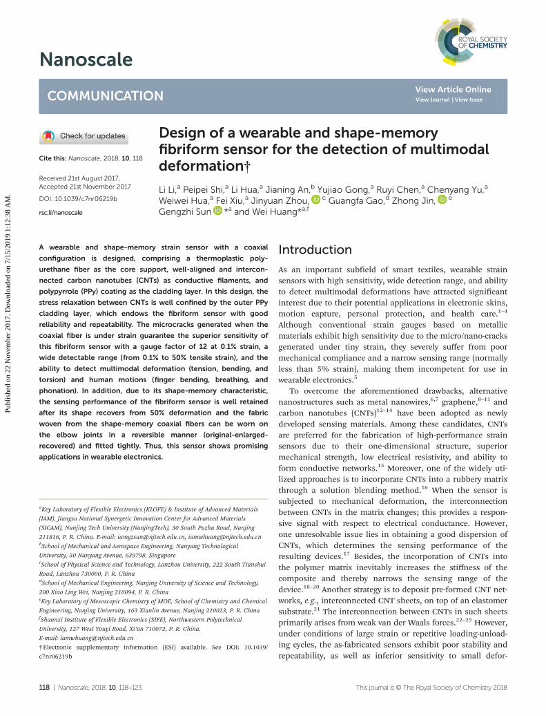
Design of a wearable and shape-memoryfibriform sensor for the detection of multimodaldeformation†
Li Li,a Peipei Shi,a Li Hua,a Jianing An,b Yujiao Gong,a Ruyi Chen,a Chenyang Yu,a
Weiwei Hua,a Fei Xiu,a Jinyuan Zhou, c Guangfa Gao,d Zhong Jin, e
Gengzhi Sun *a and Wei Huang*a,f
A wearable and shape-memory strain sensor with a coaxial
configuration is designed, comprising a thermoplastic poly-
urethane fiber as the core support, well-aligned and intercon-
nected carbon nanotubes (CNTs) as conductive filaments, and
polypyrrole (PPy) coating as the cladding layer. In this design, the
stress relaxation between CNTs is well confined by the outer PPy
cladding layer, which endows the fibriform sensor with good
reliability and repeatability. The microcracks generated when the
coaxial fiber is under strain guarantee the superior sensitivity of
this fibriform sensor with a gauge factor of 12 at 0.1% strain, a
wide detectable range (from 0.1% to 50% tensile strain), and the
ability to detect multimodal deformation (tension, bending, and
torsion) and human motions (finger bending, breathing, and
phonation). In addition, due to its shape-memory characteristic,
the sensing performance of the fibriform sensor is well retained
after its shape recovers from 50% deformation and the fabric
woven from the shape-memory coaxial fibers can be worn on
the elbow joints in a reversible manner (original-enlarged-
recovered) and fitted tightly. Thus, this sensor shows promising
applications in wearable electronics.
Introduction
As an important subfield of smart textiles, wearable strainsensors with high sensitivity, wide detection range, and abilityto detect multimodal deformations have attracted significantinterest due to their potential applications in electronic skins,motion capture, personal protection, and health care.1–4
Although conventional strain gauges based on metallicmaterials exhibit high sensitivity due to the micro/nano-cracksgenerated under tiny strain, they severely suffer from poormechanical compliance and a narrow sensing range (normallyless than 5% strain), making them incompetent for use inwearable electronics.5
To overcome the aforementioned drawbacks, alternativenanostructures such as metal nanowires,6,7 graphene,8–11 andcarbon nanotubes (CNTs)12–14 have been adopted as newlydeveloped sensing materials. Among these candidates, CNTsare preferred for the fabrication of high-performance strainsensors due to their one-dimensional structure, superiormechanical strength, low electrical resistivity, and ability toform conductive networks.15 Moreover, one of the widely uti-lized approaches is to incorporate CNTs into a rubbery matrixthrough a solution blending method.16 When the sensor issubjected to mechanical deformation, the interconnectionbetween CNTs in the matrix changes; this provides a respon-sive signal with respect to electrical conductance. However,one unresolvable issue lies in obtaining a good dispersion ofCNTs, which determines the sensing performance of theresulting devices.17 Besides, the incorporation of CNTs intothe polymer matrix inevitably increases the stiffness of thecomposite and thereby narrows the sensing range of thedevice.18–20 Another strategy is to deposit pre-formed CNT net-works, e.g., interconnected CNT sheets, on top of an elastomersubstrate.21 The interconnection between CNTs in such sheetsprimarily arises from weak van der Waals forces.22–25 However,under conditions of large strain or repetitive loading-unload-ing cycles, the as-fabricated sensors exhibit poor stability andrepeatability, as well as inferior sensitivity to small defor-
†Electronic supplementary information (ESI) available. See DOI: 10.1039/c7nr06219b
aKey Laboratory of Flexible Electronics (KLOFE) & Institute of Advanced Materials
(IAM), Jiangsu National Synergetic Innovation Center for Advanced Materials
(SICAM), Nanjing Tech University (NanjingTech), 30 South Puzhu Road, Nanjing
211816, P. R. China. E-mail: [email protected], [email protected] of Mechanical and Aerospace Engineering, Nanyang Technological
University, 50 Nanyang Avenue, 639798, SingaporecSchool of Physical Science and Technology, Lanzhou University, 222 South Tianshui
Road, Lanzhou 730000, P. R. ChinadSchool of Mechanical Engineering, Nanjing University of Science and Technology,
200 Xiao Ling Wei, Nanjing 210094, P. R. ChinaeKey Laboratory of Mesoscopic Chemistry of MOE, School of Chemistry and Chemical
Engineering, Nanjing University, 163 Xianlin Avenue, Nanjing 210023, P. R. ChinafShannxi Institute of Flexible Electronics (SIFE), Northwestern Polytechnical
University, 127 West Youyi Road, Xi’an 710072, P. R. China.
E-mail: [email protected]
118 | Nanoscale, 2018, 10, 118–123 This journal is © The Royal Society of Chemistry 2018
Publ
ishe
d on
22
Nov
embe
r 20
17. D
ownl
oade
d on
7/1
5/20
19 1
:12:
38 A
M.
View Article OnlineView Journal | View Issue

mation, due to the sliding between CNTs as a result of stressrelaxation.21 In addition, the majority of precedent strainsensors are incapable of sensing multimodal deformations(e.g., stretching, bending and twisting) simultaneously, whichhinders their application in the detection of complex bodymovements.26 Furthermore, most of the reported strainsensors are built on planar substrates, which make themunable to be tightly fitted onto complex/irregular three dimen-sional (3D) architectures, such as elbow joints and knee joints.This poses problems in electronic sensing of the dynamicmotions of the human body.26
Herein, for the first time, we develop a shape-memoryfiber sensor with a coaxial configuration consisting of thermo-plastic polyurethane (TPU) fiber as the core-support, well-aligned CNTs as conductive filaments, and polypyrrole (PPy)coating as the cladding layer. In this design, the stress relax-ation between CNTs is well confined by the outer PPy layer,which endows the fibriform sensor with good reliability andrepeatability. On the other hand, the microcracks generatedwhen the coaxial fiber is under strain guarantee the fibriformsensor high sensitivity, superior detection limit and widedetectable range for multimodal deformations (tension,bending, and torsion) and human motions (finger bending,breathing and phonation). Owing to its shape-memorycharacteristic, the fibriform sensor maintains good sensingproperties after its shape recovers from 50% deformation tothe original state. As a proof-of-concept application, a fabric isfurther woven from the shape-memory coaxial fibers, whichis worn and fitted tightly on the elbow joints in a reversiblemanner (original-enlarged-recovered).
Results and discussion
The fabrication of the shape-memory fibriform sensor isschematically illustrated in Fig. 1. The spinnable vertically-aligned CNT array with a thickness of ∼300 μm (Fig. S1†) wasprepared through chemical vapor deposition (CVD) according
to our previous studies.27–33 The TEM image (Fig. S2†) showsthat the CNTs have a mean diameter of 10 nm with multi-walls. In the Raman spectrum of the CNTs (Fig. S3†), there aretwo characteristic peaks at 1350 cm−1 and 1580 cm−1, whichcorrespond to the D and G band, respectively. The G/D radio isabout 1.05, which indicates high-quality CNTs.28 Due to theunique interconnection between the CNTs in the array,22–25 awell-aligned CNT sheet (Fig. S1b†) was continuously pulledout and cross-stacked on TPU fiber at an angle of 80° betweenthe pulling direction of the CNT sheet and the axis of the TPUfiber (Fig. S4†) to obtain the TPU@CNT fiber (Step 1).Subsequently, a thin layer of PPy was electrochemically de-posited on the outer surface of the TPU@CNT fiber to formthe TPU@CNT@PPy (TCP) fiber (Step 2).
The conductance of the TPU@CNT fiber and TCP fiber canbe facilely tuned by the number of CNT layers and electro-chemical deposition time. The well-aligned characteristic ofthe CNT sheet gives it high conductivity.32 As the number ofcross-stacked CNT layers increases, the specific length resis-tance decreases from 9.4 kΩ cm−1 for the TPU@CNT fiber withone CNT layer to 3.0 kΩ cm−1 for the TPU@CNT fiber withfour CNT layers (Fig. 2a). The outermost PPy coating wasachieved by electrochemical deposition at a constant potentialof 0.8 V. It is found that the resistance of the TCP fiberdecreases with the deposition of PPy in a time dependentmanner (Fig. 2b). The morphology change in the resultant
Fig. 1 Schematic showing the fabrication of the TCP fibriform sensor.
Fig. 2 (a) Resistance of the TPU@CNT fiber as a function of thenumber of CNT layers. (b) Resistance of TCP fibers versus electro-chemical deposition time. (c–f ) SEM images showing the morphologychange of the TCP fibers (with 4 layers of CNT sheets) with respect todeposition time.
Nanoscale Communication
This journal is © The Royal Society of Chemistry 2018 Nanoscale, 2018, 10, 118–123 | 119
Publ
ishe
d on
22
Nov
embe
r 20
17. D
ownl
oade
d on
7/1
5/20
19 1
:12:
38 A
M.
View Article Online

hybrid fibers with respect to deposition time was characterizedusing scanning electron microscopy (SEM). It can be clearlyobserved that on the surface of the TPU@CNT fiber, the CNTsare well-aligned in the same orientation (Fig. 2c). In compari-son, the surface morphology of the TCP fiber changes gradu-ally and the surface coating becomes thicker when the depo-sition time increases from 0 to 2000 s (Fig. 2d–f ). Ultimately, acoralline-like structure was formed on the surface of the TCPfiber with 2000 s deposition of PPy (denoted as TCP2000 fiber,as shown in Fig. 2f). In the cross-sectional SEM image(Fig. S5†), the coaxial structure can be observed clearly.
The strain sensing performance of the TCP fiber was testedby measuring its relative resistance variation (ΔR/R0, whereΔR = R − R0, and R0 and R are the resistance of TCP fiberbefore and after deformation, respectively) upon stretching.Compared to the TPU@CNT fiber, the TCP fibers exhibitedhigher sensitivity to tensile strain with a slightly compromiseddetectable range (Fig. 3a). Specifically, the maximum sensi-tivity was obtained with the TCP2000 fiber within the strain of60%, over which ΔR/R0 increases dramatically. This phenom-enon can be attributed to the peeling-off of the PPy layer(Fig. S6†) which leads to a rapid increase in fiber resistanceand ultimate failure of the fiber sensor. Therefore, unlessotherwise specified, the TCP2000 fiber was used for the follow-ing studies within the strain range of 0–50%. The sensingcapability of the TCP2000 fiber to stepwise tensile strain wasexamined in Fig. 3b. The ΔR/R0 value of the TCP2000 fiberupon stretching from 10% to 50% was measured to be 55% to150%, respectively, which is much higher than that of theTPU@CNT fiber. As a demonstration of direct visual obser-vation, both the TPU@CNT and TCP2000 fibers were used as
conductive wire to light an LED. Compared to the that con-nected to the TPU@CNT fiber, the LED connected to theTCP2000 fiber exhibited a more obvious change in brightnesswhen the fiber was subjected to 50% strain (Fig. S7†), whichindicating its superior sensitivity to large tensile strain.Besides, the TCP2000 fiber sensor also shows the capability forthe detection of tiny strain. The detection limit of the fibersensor was determined by applying a gradually diminishingstep strain (Fig. 3c). The ΔR/R0 value in response to the tinystrain of 0.1% was measured to be 1.2%, giving a gauge factor(GF) of 12, where GF is defined as (ΔR/R0)/ε (ε is the strain).This high detection limit makes the TCP2000 fiber sensorsuperior to the planar sensors devised using aligned single-walled CNT films on poly(dimethylsiloxane) (PDMS),14 hybri-dized films of CNT and graphene on PDMS,34 and highly-oriented CNT fiber on PDMS.13 It is also comparable to that ofthe sensor based on graphene woven fabrics on PDMS.35 Inaddition, these stepwise tensile testing results within thestrain range of 0.1% to 50% (Fig. S8†) are in good agreementwith that shown in Fig. 3a, which suggest the good repeatabil-ity of the TCP2000 fiber. Moreover, under cyclic tensile testswithin 50% strain, the TCP2000 fiber sensor shows good dura-bility and stability with ΔR/R0 retention maintained above 90%after 500 loading-unloading cycles (Fig. 3d), which is of criticalimportance for practical applications.
The microstructures of the TPU@CNT fiber and TCP2000fiber during the tensile test were characterized via SEM(Fig. 4a–f ). In the case of the TPU@CNT fiber in its originalstate, the CNTs are wound on TPU with good alignment(Fig. 4a). When the TPU@CNT fiber was subjected to 50%tensile strain, the CNTs became electrically disconnected(Fig. 4b) leading to an increase in fiber resistance. Due to the
Fig. 3 (a) Electrical responses of the TPU@CNT, TCP500, TCP1000, andTCP2000 fibers under tensile strain. (b) Resistance variations of theTPU@CNT, TCP500, TCP1000, and TCP2000 fibers under stepwise tensiletest with strain ranging from 10% to 50%. (c) Resistance variation of theTCP2000 fiber under the small tensile strain range of 0.1% to 2%. (d)Cyclic stretching–releasing tensile test of the TCP2000 fiber.
Fig. 4 SEM images of (a–c) TPU@CNT fiber and (d–f ) TPC2000 fiber inits original, 50% stretched, and released states, respectively. (g)Schematic illustration of the sensing mechanism.
Communication Nanoscale
120 | Nanoscale, 2018, 10, 118–123 This journal is © The Royal Society of Chemistry 2018
Publ
ishe
d on
22
Nov
embe
r 20
17. D
ownl
oade
d on
7/1
5/20
19 1
:12:
38 A
M.
View Article Online

irreversible sliding between CNTs under stretching,22 theCNTs became wavy even when the TPU@CNT fiber wasreleased to its original state (Fig. 4c), which explains its poorsensitivity and reliability. In comparison, with the presence ofthe PPy coating on the CNT film as a cladding layer (Fig. 4d),when the TCP2000 fiber is under tension, microcracks are gen-erated and the conductive filaments (CNTs) are well confinedby the PPy layer (Fig. 4e). Once the applied strain is released,the microcracks are closed and the electrical connectionbetween the CNTs is retained perfectly (Fig. 4f). Therefore, thesuperior sensing performance of the TCP2000 fiber (comparedto that of the TPU@CNT fiber) can be attributed to the coaxialdesign with the assistance of the PPy coating (Fig. 4g).
To demonstrate the potential of the TCP2000 fiber as a wear-able sensor for the detection of human activity, the fibersensor was fixed onto the index finger and the electrical signalof ΔR/R0 was recorded in real time when the finger was gradu-ally bent (Fig. 5a). Apparently, the increased bending magni-tude leads to a steadily increased electrical response. For cap-turing subtle physiological signals, the wearable sensors wereattached to the chest and throat. The time interval and peakamplitude in the electrical signals are presented in Fig. 5b,which were measured in the relaxation and respiration statesand reflect the respiration rate and depth, respectively. Due tothe complicated vocal cord vibration and muscle movementsaround the throat during phonation, when the tester spokedifferent words, such as “Hi”, “Hello”, and “Sensor”, theresponse curves exhibited remarkably different characteristicswith good repeatability (Fig. 5c). This indicates that theTCP2000 fiber sensor has potential applications in speech reha-bilitation training and intelligent speech recognition.36 Forsophisticated motion capture, torsion is another vital mechan-ical deformation in human joints and artificial muscles.37
Benefitting from the symmetrical structure of the CNT@PPynetwork, the TCP2000 fiber is capable of sensing torsion inboth counterclockwise and clockwise directions at differentangles with high reproducibility (Fig. 5d), which further broad-ens its applications in wearable electronics.
Generally, strain sensors constructed on planar substrateshave only a simplex shape, which is difficult to be applied on asubject with a complex structure.26 For instance, in practicalapplications, sensing devices are normally required to be fixedonto different parts of the body, e.g., finger, elbow joint, andchest. Therefore, it is highly desirable to design a sensingsystem that can readily and tightly accommodate its shape toany complex structure in addition to the commonly usedplanar surface in lab testing. Fortunately, the shape-memoryTCP fiber sensor developed in this study can be pro-grammed into a variety of shapes to be adapted to differentworking conditions. As shown in Fig. 6a, the TCP2000 fiber wasdeformed and shaped with increased radii of curvature underexternal bending stresses at a temperature above the glass tran-sition temperature (Ttrans).
38 After cooling to room tempera-ture, the polymeric network of the TPU core fiber was phys-ically cross-linked to maintain the enlarged shape.39 Uponheating at a temperature equal to or beyond Ttrans, the TCP2000fiber fully recovered to its original state due to the cleavage ofthe physical crosslinks in TPU. The sensing properties of theTCP2000 fiber sensor and that after the shape-memory processfrom 50% deformation remain almost the identical (Fig. 6b),which suggests good reliability for potential practical appli-cations. As a proof-of-concept demonstration, the textile wovenfrom TCP2000 fibers can be reversibly adapted into differentuser-required shapes and sizes, and fitted tightly to the elbowjoint, as shown in Fig. 6c.
Fig. 5 Responsive signal of the TCP2000 fibriform sensor in situ moni-toring (a) finger bending, (b) human breathing, (c) phonation, and (d)torsion at different angles.
Fig. 6 (a) Images of the shape-memory TCP2000 fibriform sensor in theoriginal, enlarged, and recovered states. (b) Sensing behavior of theTCP2000 fiber in the original and recovered states. (c) Photographsshowing the fabric woven by the shape-memory fibriform sensors,which is tightly-fitted onto the elbow of a model.
Nanoscale Communication
This journal is © The Royal Society of Chemistry 2018 Nanoscale, 2018, 10, 118–123 | 121
Publ
ishe
d on
22
Nov
embe
r 20
17. D
ownl
oade
d on
7/1
5/20
19 1
:12:
38 A
M.
View Article Online

Conclusions
In summary, we developed a fibriform strain sensor that pos-sesses the desirable integration of high sensitivity, broaddetection range in strain, superior detection limit, and thecapability of sensing multimodal mechanical deformations(tension, bending, and torsion) and monitoring humanmotions (finger bending, breathing and phonation). Inaddition, the fibriform sensor shows shape-memory charac-teristics enabling its fabric to be tightly-fitted to a nonplanarirregular subject, which has not been achieved by the planarstrain sensors reported thus. The facile, low-cost, and dry-statefabrication process, as well as the unique coaxial architectureindicate that our fiber sensor is promising for practical appli-cations in electronic skins, motion capture, personal protec-tion, and healthcare.
ExperimentalPreparation of vertically-aligned CNT arrays
Vertically-aligned CNT arrays were synthesized using a CVDprocess in a tube furnace.27–33 Typically, the growth wascarried out at 750 °C for 10 min using an Fe thin film (1 nmthick) deposited on an Si/SiO2 substrate as the catalyst, andC2H4 and Ar as the carbon source and carrier gas, respectively.
Fabrication of TPU@CNT fiber
Commercial TPU fiber (diameter of 500 μm) was used as thecore substrate. Two ends of the TPU fiber were fixed to twoelectric motors, and a CNT array was stabilized on a motorizedtranslation stage. A well-aligned CNT sheet was continuouslydrawn from the CNT array and wound around the fixed TPUfiber at an angle of 80° between the orientation of the CNTsheet and the axis of the TPU fiber. The two electric motorsand the translation stage were operated simultaneously. Thewinding velocity of the aligned CNT sheet was controlled to beequal to the moving velocity of the translation stage so that thehelical angle of the aligned CNT sheet was maintained acrossthe fiber during wrapping.
Fabrication of TCP fiber
PPy was electrodeposited onto the TPU@CNT fiber via the elec-tropolymerization of pyrrole at a constant potential of 0.8 V inan aqueous solution containing pyrrole (0.05 M), KCl (0.02 M)and HCl (0.001 M), with Ag/AgCl (saturated KCl) as the refer-ence electrode and platinum plate as the counter electrode.
Fabrication of TCP fiber based wearable sensor
The TCP fiber (2 cm in length) was placed onto a PDMS(a 10 : 1 mixture of PDMS prepolymer and curing agent,Sylgrad-184, Dow Corning) thin film. Copper wires (0.2 mm indiameter) were connected to the two ends of the TCP fiberwith the help of silver paste for in situ electrical tests.
Characterization and measurement
SEM (JEOL, JSM-7800F) was used to observe the microstructureof the fiber during stretching and after testing. TEM(JEOL-2010) and Raman Spectroscopy (WITEC, Alpha300M+)with a 633 nm laser source were used to characterize theCNTs. A microforce testing system (HY-0350, Shanghai HengYi Precise Instrument Co., Ltd) was used to apply constantstress, strain, and displacement to the strain sensor at aloading speed of 20 mm min−1. A digital source meter(Keithley 2400) was used to measure the relative resistancechange of the sensor, and the results were recorded on a com-puter using LabVIEW.
Conflicts of interest
There are no conflicts of interest to declare.
Acknowledgements
This work was supported by NanjingTech Start-Up Grant(3983500150), Jiangsu Specially-Appointed Professor program(54935012), the Natural Science Foundation of JiangsuProvince (BK20171018) and the National Natural ScienceFoundation of China (61704076, 11472008 and 11674140).
References
1 A. Chortos, J. Liu and Z. A. Bao, Nat. Mater., 2016, 15, 937–950.2 Z. N. Bao, MRS Bull., 2016, 41, 897–902.3 A. Chortos and Z. N. Bao, Mater. Today, 2014, 17, 321–331.4 M. L. Hammock, A. Chortos, B. C. K. Tee, J. B. H. Tok and
Z. A. Bao, Adv. Mater., 2013, 25, 5997–6037.5 J. Park, I. You, S. Shin and U. Jeong, ChemPhysChem, 2015,
16, 1155–1163.6 S. Lee, S. Shin, S. Lee, J. Seo, J. Lee, S. Son, H. J. Cho,
H. Algadi, S. Al-Sayari, D. E. Kim and T. Lee, Adv. Funct.Mater., 2015, 25, 3114–3121.
7 R. Ma, B. Kang, S. Cho, M. Choi and S. Baik, ACS Nano,2015, 9, 10876–10886.
8 F. Zhao, Y. Zhao, H. H. Cheng and L. T. Qu, Angew. Chem.,Int. Ed., 2015, 54, 14951–14955.
9 Y. Cheng, R. R. Wang, J. Sun and L. Gao, Adv. Mater., 2015,27, 7365–7371.
10 Q. Liu, J. Chen, Y. R. Li and G. Q. Shi, ACS Nano, 2016, 10,7901–7906.
11 C. Y. Yan, J. X. Wang, W. B. Kang, M. Q. Cui, X. Wang,C. Y. Foo, K. J. Chee and P. S. Lee, Adv. Mater., 2014, 26,2022–2027.
12 J. Foroughi, G. M. Spinks, S. Aziz, A. Mirabedini,A. Jeiranikhameneh, G. G. Wallace, M. E. Kozlov andR. H. Baughman, ACS Nano, 2016, 10, 9129–9135.
13 S. Ryu, P. Lee, J. B. Chou, R. Z. Xu, R. Zhao, A. J. Hart andS. G. Kim, ACS Nano, 2015, 9, 5929–5936.
Communication Nanoscale
122 | Nanoscale, 2018, 10, 118–123 This journal is © The Royal Society of Chemistry 2018
Publ
ishe
d on
22
Nov
embe
r 20
17. D
ownl
oade
d on
7/1
5/20
19 1
:12:
38 A
M.
View Article Online

14 T. Yamada, Y. Hayamizu, Y. Yamamoto, Y. Yomogida,A. Izadi-Najafabadi, D. N. Futaba and K. Hata, Nat.Nanotechnol., 2011, 6, 296–301.
15 D. J. Lipomi, M. Vosgueritchian, B. C. K. Tee,S. L. Hellstrom, J. A. Lee, C. H. Fox and Z. N. Bao,Nat. Nanotechnol., 2011, 6, 788–792.
16 S. Jung, J. H. Kim, J. Kim, S. Choi, J. Lee, I. Park, T. Hyeonand D. H. Kim, Adv. Mater., 2014, 26, 4825–4830.
17 S. Park, M. Vosguerichian and Z. A. Bao, Nanoscale, 2013,5, 1727–1752.
18 P. D. Bradford, X. Wang, H. B. Zhao, J. P. Maria, Q. X. Jiaand Y. T. Zhu, Compos. Sci. Technol., 2010, 70, 1980–1985.
19 J. J. Ge, H. Q. Hou, Q. Li, M. J. Graham, A. Greiner,D. H. Reneker, F. W. Harris and S. Z. D. Cheng, J. Am.Chem. Soc., 2004, 126, 15754–15761.
20 Q. F. Cheng, M. Z. Li, L. Jiang and Z. Y. Tang, Adv. Mater.,2012, 24, 1838–1843.
21 F. Xu, X. Wang, Y. T. Zhu and Y. Zhu, Adv. Funct. Mater.,2012, 22, 1279–1283.
22 G. Z. Sun, L. X. Zheng, J. Y. Zhou, Y. N. Zhang, Z. Y. Zhanand J. H. L. Pang, Int. J. Plast., 2013, 40, 56–64.
23 X. B. Zhang, K. L. Jiang, C. Teng, P. Liu, L. Zhang, J. Kong,T. H. Zhang, Q. Q. Li and S. S. Fan, Adv. Mater., 2006, 18,1505–1510.
24 M. Zhang, S. L. Fang, A. A. Zakhidov, S. B. Lee, A. E. Aliev,C. D. Williams, K. R. Atkinson and R. H. Baughman,Science, 2005, 309, 1215–1219.
25 L. Hua, Z. Y. Ma, P. P. Shi, L. Li, K. Rui, J. Y. Zhou,X. Huang, X. Liu, J. X. Zhu, G. Z. Sun and W. Huang,J. Mater. Chem. A, 2017, 5, 2483–2487.
26 M. Amjadi, K. U. Kyung, I. Park and M. Sitti, Adv. Funct.Mater., 2016, 26, 1678–1698.
27 P. P. Shi, L. Li, L. Hua, Q. Q. Qian, P. F. Wang, J. Y. Zhou,G. Z. Sun and W. Huang, ACS Nano, 2017, 11, 444–452.
28 G. Z. Sun, Y. X. Huang, L. X. Zheng, Z. Y. Zhan,Y. N. Zhang, J. H. L. Pang, T. Wu and P. Chen, Nanoscale,2011, 3, 4854–4858.
29 G. Z. Sun, J. Q. Liu, L. X. Zheng, W. Huang and H. Zhang,Angew. Chem., Int. Ed., 2013, 52, 13351–13355.
30 G. Z. Sun, X. Zhang, R. Z. Lin, B. Chen, L. X. Zheng,X. Huang, L. Huang, W. Huang, H. Zhang and P. Chen,Adv. Electron. Mater., 2016, 2, 1600102.
31 G. Z. Sun, X. Zhang, R. Z. Lin, J. Yang, H. Zhang andP. Chen, Angew. Chem., Int. Ed., 2015, 54, 4651–4656.
32 G. Z. Sun, L. X. Zheng, J. An, Y. Z. Pan, J. Y. Zhou,Z. Y. Zhan, J. H. L. Pang, C. K. Chua, K. F. Leong and L. Li,Nanoscale, 2013, 5, 2870–2874.
33 Q. Qian, Q. Hu, L. Li, P. Shi, J. Zhou, J. Kong, X. Zhang,G. Sun and W. Huang, Sens. Actuators, B, 2018, 257,23–28.
34 J. D. Shi, X. M. Li, H. Y. Cheng, Z. J. Liu, L. Y. Zhao,T. T. Yang, Z. H. Dai, Z. G. Cheng, E. Z. Shi, L. Yang,Z. Zhang, A. Y. Cao, H. W. Zhu and Y. Fang, Adv. Funct.Mater., 2016, 26, 2078–2084.
35 Y. Wang, L. Wang, T. T. Yang, X. Li, X. B. Zang, M. Zhu,K. L. Wang, D. H. Wu and H. W. Zhu, Adv. Funct. Mater.,2014, 24, 4666–4670.
36 D. Kang, P. V. Pikhitsa, Y. W. Choi, C. Lee, S. S. Shin,L. F. Piao, B. Park, K. Y. Suh, T. I. Kim and M. Choi, Nature,2014, 516, 222–226.
37 J. Foroughi, G. M. Spinks, G. G. Wallace, J. Oh,M. E. Kozlov, S. L. Fang, T. Mirfakhrai, J. D. W. Madden,M. K. Shin, S. J. Kim and R. H. Baughman, Science, 2011,334, 494–497.
38 M. Behl, M. Y. Razzaq and A. Lendlein, Adv. Mater., 2010,22, 3388–3410.
39 J. E. Deng, Y. Zhang, Y. Zhao, P. N. Chen, X. L. Cheng andH. S. Peng, Angew. Chem., Int. Ed., 2015, 54, 15419–15423.
Nanoscale Communication
This journal is © The Royal Society of Chemistry 2018 Nanoscale, 2018, 10, 118–123 | 123
Publ
ishe
d on
22
Nov
embe
r 20
17. D
ownl
oade
d on
7/1
5/20
19 1
:12:
38 A
M.
View Article Online