Embed Size (px)
Citation preview

Design of a MOSFET-Based Pulsed Power
Supply for Electroporation
by
Jason R. Grenier
A thesis
presented to the University of Waterloo
in fulfillment of the
thesis requirement for the degree of
Master of Applied Science
in
Electrical and Computer Engineering
Waterloo, Ontario, Canada, 2006
©Jason R. Grenier, 2006

ii
I hereby declare that I am the sole author of this thesis. This is a true copy of the thesis, including any
required final revisions, as accepted by my examiners.
I understand that my thesis may be made electronically available to the public.

iii
Abstract
The use of high-voltage pulsed electric fields in biotechnology and medicine has lead to new
methods of cancer treatment, gene therapy, drug delivery, and non-thermal inactivation of
microorganisms. Regardless of the application, the objective is to open pores in the cell membrane
and hence either facilitate the delivery of foreign materials inside the cell, or to kill the cell
completely. Pulsed power supplies are needed for electroporation, which is the process of applying
pulsed electric fields to biological cells to induce a temporary permeability in the cell membrane. The
applications of pulsed electric fields are dependent on the output pulse shape and pulse parameters,
both of which can be affected by the circuit parameters of the pulsed power supply and the
conductivity of the media being treated.
In this research, two Metal Oxide Field Effect Transistor (MOSFET)-based pulsed power supplies
that are used for electroporation experiments were designed and built. The first used up to three
MOSFETs in parallel to deliver high voltage pulses to highly conductive loads. To produce pulses
with higher voltages, a second pulsed power supply using two MOSFETs connected in series was
designed and built. The parallel and series MOSFET-based pulsed power supplies are capable of
producing controllable square pulses with widths of a few hundred nanoseconds to dc and amplitudes
up to 1500 V and 3000 V, respectively. The load in this study is a 1-mm electroporation cuvette filled
with a buffer solution that is varied in conductivity from 0.7 mS/m to 1000 mS/m. The results
indicate that by controlling the circuit parameters such as the number of parallel MOSFETs, gate
resistance, energy storage capacitance, and the parameters of the MOSFET driver gating pulses, the
output pulse parameters can be made almost independent of the load conductivity.
Using the pulsed power supplies designed in this work, an investigation into electroporation-
mediated delivery of a plasmid DNA molecule into the pathogenic bacterium E. coli O157:H7, was
conducted. It was concluded that increasing the electric field strength and pulse amplitude resulted in
an increase in the number of transformants. However, increasing the number of pulses had the effect
of reducing the number of transformants. In all of the experiments, the number of cells that were
inactivated by the exposure to the pulsed electric field was measured.

iv
Acknowledgements
First and foremost, I would like to thank my supervisors Dr. Shesha Jayaram and Dr. Mehrdad
Kazerani for their guidance and support throughout my graduate studies. Their approach to teaching
and research has inspired me to continue graduate studies and to continue to share my knowledge
with others.
I must also acknowledge the Canadian Research Institute for Food Safety (CRIFS) at the
University of Guelph, for the use of their facilities and their willingness to train an Electrical Engineer
in the techniques of microbiology. I am also indebted to Dr. Haifeng Wang, a researcher at CRIFS.
Without his cooperation, time and knowledge, which he shared very generously, the experimental
work on electroporation-mediated plasmid DNA delivery would not have been possible.
I am also grateful to Dr. John Yeow and Dr. Siva Sivoththaman for reviewing this thesis within the
required timeframe.
I would also like to thank my fellow colleagues in the High-Voltage lab: Saeed, Ayman, Fermin,
Ali, Mostafa, and Yuseph, you all contributed to my learning experience. Thank you for your advice
and the many intellectual conversations during daily tea time in the CPH foyer.
To all of my friends from home and in the community at St. Paul’s College, thank you for your
constant and endless support in all aspects of my life. A special thank you to Tammy for proofreading
this thesis and for her constant support and understanding which has enriched my life. Finally, I must
thank my parents for their love, support and positive attitude; they are a constant source of motivation
and inspiration for me.

v
Table of Contents Abstract......................................................................................................................................iii
Acknowledgements ................................ ................................ ................................ ..................... iv
Table of Contents .........................................................................................................................v
List of Tables .............................................................................................................................vii
List of Figures................................ ................................ ................................ ...........................viii
Chapter 1 Introduction ..................................................................................................................1
1.1 Background ........................................................................................................................1
1.1.1 Electroporation .............................................................................................................1
1.1.2 Fundamentals of Pulsed Power Supplies .........................................................................4
1.2 Aim of the Present Work and Thesis Organization.................................................................5
Chapter 2 Experimental Setup .......................................................................................................8
2.1 Design of the Pulsed power supply Circuit ............................................................................8
2.1.1 Power and Control Module ............................................................................................8
2.1.2 MOSFET Driver and MOSFET................................ ................................ ....................12
2.1.3 Pulsed power supply Using Parallel MOSFETs.............................................................13
2.1.4 Connecting MOSFETs in Series for Increased Voltage Capability ..................................16
2.2 Modeling of the Electroporation Loads ...............................................................................20
2.3 Electroporation of Escherichia coli O157:H7 ......................................................................21
2.3.1 Preparation of Electrocompetent Cells ..........................................................................21
2.3.2 Electroporation Protocol..............................................................................................22
2.3.3 Plating and Counting ...................................................................................................23
Chapter 3 Results........................................................................................................................24
3.1 Varying the Conductivity of the Load .................................................................................24
3.1.1 Effect on the Pulse Amplitude ......................................................................................25
3.1.2 Effect on the Rise and Fall Times of the Pulse...............................................................26
3.1.3 Effect on the Pulse Width ................................ ................................ ............................28
3.2 Varying the MOSFET Gate Resistance...............................................................................29
3.2.1 Effect on the Pulse Amplitude ......................................................................................30
3.2.2 Effect on the Rise and Fall Times of the Pulse...............................................................31
3.2.3 Effect on the Pulse Width ................................ ................................ ............................32
3.3 Varying the Energy Storage Capacitance................................ ................................ ............33
vi
3.3.1 Effect on the Pulse Amplitude ......................................................................................34
3.3.2 Effect on the Rise and Fall Times of the Pulse...............................................................35
3.3.3 Effect on the Pulse Width ................................ ................................ ............................36
3.4 Electroporation of Escherichia coli O157:H7 ......................................................................37
3.4.1 Experiment #1: Two 1.35-MV/m Microsecond Pulses ...................................................38
3.4.2 Experiment #2: Multiple 1.35-MV/m Microsecond Pulses.............................................38
3.4.3 Experiment #3: Single 2.15-MV/m Microsecond Pulses ................................................41
3.4.4 Experiment #4: Increasing the Number of 2.15-MV/m, 1-ms Pulses ...............................43
Chapter 4 Discussion ..................................................................................................................47
4.1 Using Pulsed Power Supplies With Conductive Loads .........................................................47
4.2 Paralleling MOSFETs to Reduce the Loading Effect................................ ............................51
4.3 Varying the Gate Resistance to Control the Rise and Fall Times of the Pulse.........................52
4.4 Choosing an Energy Storage Capacitor ...............................................................................53
4.5 Improving Electroporation-Mediated Plasma DNA molecule Delivery..................................55
4.5.1 Effect of Pulse Width on Electroporation ......................................................................56
4.5.2 Effect of the Number of Pulses on Electroporation ........................................................57
Chapter 5 Conclusions and Future Research.................................................................................59
5.1 Conclusions ......................................................................................................................59
5.2 Future Research ................................................................................................................61
References .................................................................................................................................62
Appendix A Microcontroller Code ...............................................................................................66
Appendix B Electroporation Protocol...........................................................................................70
B.1 Preparation of Electrocompetent Cells ................................................................................70
B.2 Electroporation.................................................................................................................71
B.3 Solutions and Reagents.....................................................................................................72

vii
List of Tables
Table 3.1: Results of the first set of electroporation experiments to study the effect of increasing
the pulse width of two 1.35-MV/m pulses on the survival ratio and number of
transformants ..........................................................................................................38
Table 3.2: Results of the second set of electroporation experiments to study the effect of
increasing the pulse width of multiple 1.35-MV/m pulses on the survival ratio and
number of transformants. .........................................................................................40
Table 3.3: Results of the third set of electroporation experiments to study the effect of increasing
the pulse width of a single 2.15-MV/m pulses on the cell survival ratio and number
of transformants......................................................................................................42
Table 3.4: Results of the fourth set of electroporation experiments to study the effect of the
number of 1-ms, 2.15-MV/m pulses on the survival ratio and number of
transformants ..........................................................................................................45

viii
List of Figures
Figure 1.1: Process of pore formation: (a) normal cell membrane, (b) a cell excited by short
electrical pulse resulting in irregular molecular structure, (c) the membrane being
notched, (d) the cell with a temporary hydrophobic pore, and (e) the cell with a
hydrophilic pore after membrane restructuring [5]. ................................ ......................2
Figure 1.2: Applications of pulsed electric fields for various electric strength and pulse widths
[8] ............................................................................................................................3
Figure 2.1: Power and control module of the pulsed power supply ..................................................9
Figure 2.2: Circuit Diagram for the 15-Vdc and 5-Vdc power supplies ..........................................10
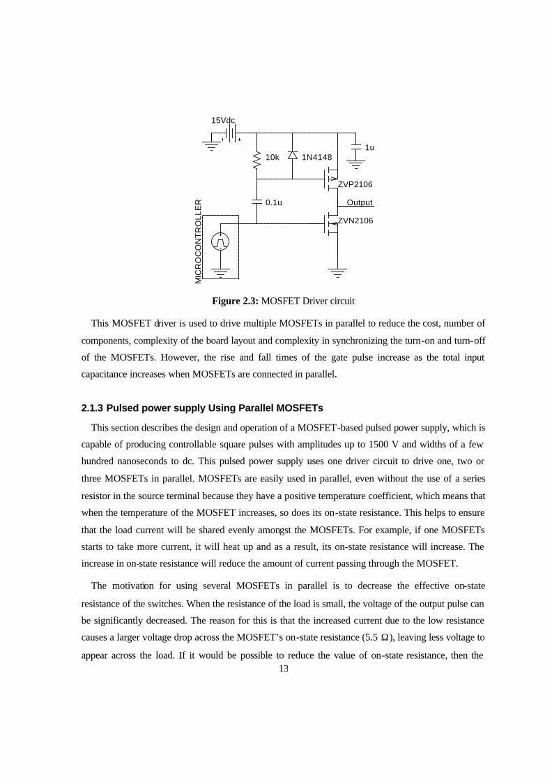
Figure 2.3: MOSFET Driver circuit ................................ ................................ ............................13
Figure 2.4: Circuit diagram of the parallel-MOSFET pulsed power supply ................................ ....14
Figure 2.5: Picture of the three parallel-MOSFET pulsed power supply circuit board .....................15
Figure 2.6: Circuit diagram of the series-MOSFET pulsed power supply .......................................17
Figure 2.7: Picture of the series-MOSFET pulsed power supply................................ ....................17
Figure 2.8: (a) picture and (b) model of a1-mm gap electroporation cuvette ...................................20
Figure 3.1: Measured output voltage waveforms with a load conductivity of 0.7 mS/m using (A)
the parallel-MOSFET and (B) the series-MOSFET pulsed power supply. ....................25
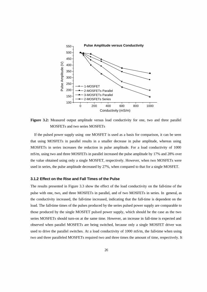
Figure 3.2: Measured output amplitude versus load conductivity for one, two and three parallel
MOSFETs and two series MOSFETs........................................................................26
Figure 3.3: Measured output fall-time versus load conductivity for one, two and three parallel
MOSFETs and two series MOSFETs........................................................................27
Figure 3.4: Measured output rise-time versus load conductivity for one, two and three parallel
MOSFETs and two series MOSFETs........................................................................28
Figure 3.5: Measured output pulse width versus load conductivity for one, two and three parallel
MOSFETs and two series MOSFETs........................................................................29
Figure 3.6: Measured output pulse amplitude versus the gate resistance for load conductivities
of 0.7 mS/m to 600 mS/m. .......................................................................................30
Figure 3.7: Measured output pulse fall-time versus the gate resistance for load conductivities of
0.7 mS/m to 1000 mS/m. .........................................................................................31
Figure 3.8: Measured output pulse rise-time versus the gate resistance for load conductivities of
0.7 mS/m to 1000 mS/m. .........................................................................................32

ix
Figure 3.9: Measured output pulse width versus the gate resistance for load conductivities of
0.7 mS/m to 1000 mS/m. .........................................................................................33
Figure 3.10: Measured output voltage amplitude versus energy storage capacitance for load
conductivities of 0.7 mS/m to 1000 mS/m. ................................................................34
Figure 3.11: Measured fall-time versus energy storage capacitance for load conductivities of 0.7
mS/m to 1000 mS/m. ...............................................................................................35
Figure 3.12: Measured rise-time versus energy storage capacitance for load conductivities of
0.7 mS/m to1000 mS/m. ..........................................................................................36
Figure 3.13: Measured output pulse width versus energy storage capacitance for load
conductivities of 0.7 mS/m to 1000 mS/m. ................................................................37
Figure 3.14: Selective plates showing the cells that have been transformed. The samples that
were plated have been diluted 10 times................................. ................................ ....39
Figure 3.15: Non-selective plates showing the total number of surviving cells. The samples that
were plated have been diluted 108 times. ...................................................................39
Figure 3.16: The effect of increasing the pulse width of multiple 1.35-MV/m pulses on the cell
survival ratio and number of transformants................................................................41
Figure 3.17: Selective plates showing the cells that have been transformed. The samples that
were plated have been diluted 102 times. ...................................................................42
Figure 3.18: Non-selective plates showing the total number of surviving cells. The samples that
were plated have been diluted 107 times. ...................................................................42
Figure 3.19: The effect of increasing the pulse width of a single 2.15-MV/m pulse on the
survival ratio and number of transformants................................................................43
Figure 3.20: Selective plates showing the cells that have been transformed. The samples that
were plated have been diluted 10 times................................. ................................ ....44
Figure 3.21: Non-selective plates showing the total number of surviving cells. The samples that
were plated have been diluted 106 times. ...................................................................44
Figure 3.22: Graph showing the effect of increasing the pulse width of 1-ms, 2.15-MV/m pulses
on the survival ratio and number of transformants......................................................46
Figure 4.1: Measured output voltage pulse from a single MOSFET pulsed power supply with a
load conductivity of (A): 0.7 mS/m and (B): 1000 mS/m................................ ............48
Figure 4.2: Pulse amplitude versus load conductivity of the MOSFET-based pulsed power
supplies used in this research and the Gene Pulser. ................................ ....................49

x
Figure 4.3: Channel 1 and 2: The measured gate-source voltage before and after the 4-Ω gate
resistor for the single MOSFET pulsed power supply with a load conductivity of
0.7 mS/m. Channel M: the difference between channels 1 and 2, is proportional to
the MOSFET gate current. .......................................................................................53
Figure 4.4: Measured output voltage pulse from a single MOSFET pulsed power supply with a
load conductivity of 45 mS/m and an energy storage capacitor of (A): 100 nF and
(B): 1500 nF, charged to 500 V. ..................................................................................54

1
Chapter 1
Introduction
The use of pulsed electric fields (PEFs) has found applications in biotechnology, medicine, food
processing and industrial applications. The use of PEFs in food processing applications has led to a
new method of non-thermal inactivation of microorganisms. Industrial applications of PEFs include
the filtering of flue gas particles using electrostatic precipitators. The use of high-voltage pulsed
electric fields in biotechnology and medicine, which is the focus in this thesis, has lead to new
methods of cancer treatment, gene therapy, drug delivery, and non-thermal inactivation of
microorganisms. Regardless of the application, the objective is to open pores in the cell membrane
and hence, either facilitate the delivery of foreign materials inside the cell or to kill the cell
completely. Pulsed power supplies that capable of producing high voltage controllable pulses are
needed for electroporation.
1.1 Background
This section provides the necessary background information to form an understanding of pulsed
power supplies and the applications for which they are used, in the context of the research completed
in this thesis.
1.1.1 Electroporation
Electroporation is the process of applying pulsed electric fields to biological cells to induce a
permeability in the cell membrane. The process can be reversible or irreversible depending on, if the
permeability is temporary and able to reseal, or permanent, causing the membrane to rupture.
However, the mechanisms by which these pores are created and the origin of such pores are not fully
understood and still controversial [1-3]. The discussion below reveals two different schools of
thought for membrane breakdown. A comprehensive review of the theory of electroporation is
available in [4].
One explanation for the process of electroporation is an increase in the transmembrane voltage is
believed to result in a temporary aqueous pathway across the membrane. Figure 1.1 illustrates the
lipid bilayer of cell membranes destabilizing under the influence of a pulsed electric field to form a
pore, which is one of the proposed models of electroporation.

2
Figure 1.1: Process of pore formation: (a) normal cell membrane, (b) a cell excited by short electrical
pulse resulting in irregular molecular structure, (c) the membrane being notched, (d) the
cell with a temporary hydrophobic pore, and (e) the cell with a hydrophilic pore after
membrane restructuring [5].
Zimmermann [6-7] proposed another model for electroporation, which is based on the
electromechanical compression of the cell membrane. The pulsed electric field creates an attraction of
opposite charges induced on the inner and outer membrane, thus creating a compressive force. If the
strength and the duration of the field are high enough, the compressive force can cause the lipid
bilayer to become permeable to the medium.
Pulse width and electric field strength are two very important parameters and the ability to control
them in different ranges is a useful property of a pulsed power supply. The importance of the
flexibility of the pulse width and electric field strength is shown in Figure 1.2, which shows the
combination of these parameters that are needed for different applications.

3
Figure 1.2: Applications of pulsed electric fields for various electric strength and pulse widths [8]
The pore opening during electroporation allows for the insertion of drugs or genes into the cell [8].
Pulses having widths of 100 µs, and electric field strengths of 100 kV/m have been effective in
delivering drugs to mammalian cells; whereas, 20-ms, 5-kV/m pulses have been effective in gene
delivery [9]. If the electric field strength exceeds the critical breakdown strength, the membrane will
be irreversibly damaged and the cell will die. Pulses in the microsecond range, with electric field
intensities in the tens of megavolts per meter, have been reported to kill bacteria in water and liquid
foods [8]. Recently, the ability to control the pulse width in the nanosecond region has received
increased attention due to the fact that pulses in the range of nanoseconds with electric field
intensities in the range of several megavolts per meter are able to manipulate the inner structures of
the biological cell, a process known as intracellular electromanipulation [10,11]. Also, nanosecond
pulses could be used for applications ranging from gene therapy to selected apoptosis induction and
tumour growth inhibition [12]. A comprehensive review of medical applications of electroporation is
available in [13].
There are many pulse parameters such as electric field strength, pulse width, pulse shape, rise time,
number of pulses per second, and time interval between the pulses that influence the process of

4
electroporation. However, the most important parameters for effective electroporation are pulse width
and the electric field strength [8,9]. In addition, a fast rise time is also beneficial for applications
requiring pulses in the sub-nanosecond regime [14]. The key point is that the pulse parameters must
be highly controllable to get the optimal pore size and pore population, and avoid rupturing the cell
membrane causing the cell to be irreversibly damaged. The shape of the pulse also influences the
results in the applications of pulsed electric fields [15]. Therefore, pulsed power supplies that are
capable of controlling many of the important pulse parameters over a wide range and provide certain
pulse shapes, regardless of the medium conductivity, are highly desirable.
1.1.2 Fundamentals of Pulsed Power Supplies
The fundamental purpose of a pulsed power supply is to convert a low peak-power, long duration
input pulse into a high peak-power, short duration pulse. To accomplish this, the following
components are needed: a high-voltage power supply, an energy storage device, pulse compression
stage, impedance matching stage, a switch, and finally the load [16].
The high voltage power supply provides the energy that is to be stored in the energy storage device,
which in this research is a capacitor. Pulsed power supplies that use inductive storage devices are not
in the scope of this research, but are reviewed in [16]. The energy is stored in the capacitor until the
pulse is needed at which time the switch must close. When this happens, the energy goes through a
pulse compression stage or multiple stages, where the total energy is discharged in a short time. The
ideal case would be that all of the energy that is put into the systems is at the output; however, this is
not the case, because real devices have parasitic losses. Good designs make use of circuit techniques
to minimize these losses. One example is impedance matching, which is a condition for maximum
power transfer. The performance of the pulsed power supply can be assessed by its voltage amplitude,
rise-time, fall-time, pulse width, repetition rate, peak power and average power.
Early pulsed power supplies used tube -based switches such as thyratrons because of their high
voltage capabilities and fast turn-on times. However, with a thyratron switch, only the turn-on time is
controllable, leaving the turn-off time dependent on the RC time constant of the load resistance and
the energy storage capacitor, leading to an exponential-decay pulse. Square pulses are more desirable
than exponential pulses of the same energy because more of that energy is delivered at higher field
strength, which is above the threshold field for the application. Thyratron-based pulsed power
supplies can use a pulse forming network (PFN) in order to deliver a square pulse. However, the PFN

5
can only be tuned to a single pulse width. Modifications are required for each pulse width that is
required. In addition, the PFN adds components to the system, which increases the cost and losses of
the circuit. Advances in semiconductor switches have lead to devices with higher voltage and current
ratings. Although semiconductor devices do not have as high voltage ratings as tube -based devices,
they can be stacked in series to obtain the required voltage ratings. Semiconductor switches have
controllable turn-on and turn-off, which allows them to produce square pulses of controllable widths.
A comparison between a semiconductor-based and a thyratron-based pulsed power supply is available
in [17]. Semiconductor switches also have the advantage of higher repetition rates and longer
lifetimes. In this regard, a recent trend has been to use power semiconductor devices, mainly the
Metal Oxide Semiconductor Field Effect Transistors (MOSFETs) and Insulated Gate Bipolar
Transistors (IGBTs), for pulsed power supplies to be used for biotechnology and medical
applications. Reference [18] tested several MOSFETs and IGBTs for use in pulse applications and
noticed that MOSFETs were capable of faster turn-on and turn-off times but had lower voltage and
current ratings than IGBTs. A single IGBT-based pulsed power supply was used in [19] to investigate
the viability of Escherichia coli (E. coli) after exposure to 1.3-MV/m and 1.5-MV/m pulsed electric
fields of 4 µs to 32 µs in duration. A single MOSFET-based pulsed power supply capable of
producing nanosecond pulses up to 400 V was designed and built in [14]. The design emphasis was
focused on a compact device that had control over the pulse shape. A similar 400-V nanosecond
pulsed power supply for use with electroporation-mediated drug and gene delivery was presented in
[20]. The pulsed power supply was capable of produces nanosecond to microsecond pulses into a 50-
Ω load. In order to overcome the lower voltage ratings of the MOSFET-based pulsed power supplies,
[21] designed, simulated and built a pulsed power supply using several MOSFETs in series to
increase the voltage capabilities of the device. The pulsed power supply was capable of produces
square pulses up to 1500 V while maintaining both static and dynamic voltage balancing. Using the
topology presented in [21] a similar device using four MOSFETs in series capable of produced 1500
V square pulses was presented [22]. Simulation results showed the effects of varying the load
resistance on the output pulse parameters.
1.2 Aim of the Present Work and Thesis Organization
New applications of pulsed electric fields are often realized when pulses with different parameters
are applied. In addition, the optimization of experiments and processes require the ability to vary the
pulse parameters in a controlled manner. The motivation for this work comes from the fact that “the

6
pulsed power community has not been strongly involved in the development of pulsed power systems
for bioelectrics, …the development of pulsed power instrumentation for medical and biological
research was left to a large extent to clinicians and biologists [8].” As the application of pulsed
electric fields develop from laboratory-controlled experiments to in vivo applications, the control on
the load conditions and parameters decreases. As a result, pulse power supplies that are capable of
controlling many of the important pulse parameters over a wide range, and provide certain pulse
shapes regardless of the load conductivity, are highly desirable. Therefore, the research in this thesis
is focused on designing a pulsed power supply that is capable of producing pulses that can be
controlled, and are less dependent on the load. The pulse power supplies designed and built in this
research are used for experiments on electroporation-mediated plasmid DNA molecule delivery in E.
Coli O157:H7 (ATCC 43888). E. coli O157:H7 was first recognized as a food-borne pathogen in
1982, when it was associated with consumption of improperly cooked ground beef [23]. The reason
for which E. Coli O157:H7 was chosen for this research, was its degree of resistance to
transformation, leaving the potential for significant improvements using a more controlled pulsed
power supply.
More specifically, the objectives of the thesis are as follows:
• To design a MOSFET-based pulsed power supply capable of producing square pulses with
amplitudes up to 3000 V and widths of a few hundred nanoseconds to dc.
• To provide a high degree of control of the pulse amplitude, pulse width, number of pulses
and the time between pulses.
• To investigate the effects of the circuit and load parameters on the output pulses and make
the pulses less dependent on the load conductivity.
• To use the pulsed power supplies that were designed and built in this research to
investigate the effects of different pulse parameters on the electroporation-mediate plasmid
DNA delivery.
• To improve the transformation of E. Coli O157:H7 with pGFPuv plasmid DNA molecule.
With respect to the abovementioned objectives, this thesis is organized as follows:
• Chapter 2 explains the design of the two pulsed power supplies that are designed and built
in this research. In addition, the power and control module that provides each pulsed power

7
supply with its necessary low voltage power and control signals is explained. A model for
the load, an electroporation cuvette, is also presented. Finally, the setup of the
electroporation-mediated plasmid DNA delivery into E. coli O157:H7 is presented. This
inclu des the preparation of electrocompetent cells, the electroporation protocol, and the
method of plating and counting.
• Chapter 3 presents the results of varying the circuit and load parameters on the output
pulses produced by the MOSFET-based pulsed power supplies. Specifically, the effect of
varying the load conductivity, gate resistance, and energy storage capacitance on the pulse
amplitude, rise and fall times, and pulse width are discussed. The results of the
electroporation-mediated plasmid DNA delivery experiments are presented as four separate
experiments, each consisting of several trails for which different pulses were used. The
results show the number of transformants and the survival ratio for different pulse widths,
amplitude, and number of pulses.
• Chapter 4 provides the analysis and discussion of the results presented in the previous
chapter. This enables the important factors that influence the pulse parameters and the
electroporation experiments to be identified. In this chapter, the focus is on explaining the
results in detail, and whenever possible, comparing them to similar studies. In addition, the
results are applied to explain the results and trends that have been reported in the literature.
• Chapter 5 is a summary of this thesis and provides some suggestions for future work.

8
Chapter 2
Experimental Setup
This chapter provides the necessary information to understand the circuits that were designed and
built, and the application for which they were used. The first section describes the pulsed power
supply circuit, one module at a time, while the second section describes the modeling of the load used
for the electroporation experiments. The final section contains the preparation, protocol and analysis
methods used to conduct an investigation into the electroporation-mediated plasmid DNA molecule
delivery into E. coli.
2.1 Design of the Pulsed power supply Circuit
This section describes the design, construction and operation of each of the modules of the pulsed
power supply circuits that were used in this research. There are two pulsed power supplies that were
designed and constructed; one with series connected and the other with parallel connected MOSFETs.
A modular design is used to build the two pulsed power supplies so that they can use the same power
supplies, control signals and energy storage capacitor.
2.1.1 Power and Control Module
The power and control module enables the pulsed power supply to be connected to, and be
powered from, a standard 110-Vrms electrical outlet. This increased flexibility allows the pulsed
power supply to function in any laboratory, an important feature because any work requiring
microorganisms should be conducted in a microbiology laboratory. This module replaces two external
dc sources, a 15-Vdc power supply necessary to operate the MOSFET driver circuit and a 5-Vdc
power supply needed to power the microcontroller. This module contains a microcontroller that
replaces the function generator that was initially used to vary the width of the pulses and the number
of pulses per second. A picture of the power and control module is illustrated in Figure 2.1.

9
Figure 2.1: Power and control module of the pulsed power supply
2.1.1.1 Power Supplies
To function properly, the microcontroller and the MOSFET driver require a 5-Vdc and a 15-Vdc
power supply, respectively. These supplies are built as part of the power and control module to make
the device more compact and less dependent on external components. Also, building the 15-Vdc
power supply for the MOSFET driver ensures that it is capable of supplying the required gate current,
in the required amount of time, during the turn-on and turn-off periods of the MOSFET. The only
external source that is needed for the pulsed power supply is the high voltage dc source that is used to
charge the energy storage capacitor. For this purpose, the WX5R200 5-kV, 200-mA high voltage dc
source manufactured by Glassman High Voltage, Inc. was used. The reasons for using a commercial
high voltage dc source were: to save time in order to focus on the actual pulsed power supply circuit
and to take advantage of the safety interlocks that are built -in to the commercial source.
The power and control module is connected to standard 110-Vrms, 60-Hz electrical outlet and the
power is converted to dc using a conventional ac-to-dc converter and a voltage regulator. Figure 2.2
illustrates the circuit schematic that was used to produce the 15 Vdc and 5 Vdc from the standard
110-Vrms outlet.
PIC18LF458
Start Button Power ON/OFF
5-V Regulator
Transformer 15-V Regulator

10
Figure 2.2: Circuit Diagram for the 15-Vdc and 5-Vdc power supplies
The 24-VA transformer has two secondary winding that were used separately to avoid the use of
two separate transformers. The transformer has a primary voltage of 115 V, and a secondary voltage
of 15 V. When the power and control module is initially turned on, the discharged filter capacitor
appears as a short circuit, which may result in a large inrush current and significant over-voltages.
This can cause damage to the diodes in the rectifier bridge, the filter capacitor, or the load to which
the power supply is connected. To limit the inrush current, a 50-Ω thermistor is placed in series
between the rectifier bridge and the filter capacitor. When the thermistor is cold it has a resistance of
50 Ω. The resistance decreases to almost zero as current flows through it raising its temperature. The
50-Ω thermistor was selected based on the criterion that the inrush current should be less than 1 A, as
all of the components will be rated above this value. The worst case occurs when the capacitor is
completely discharged and the source is at its peak voltage value at the moment of turn-on. Circuit
analysis [24] confirms that the theoretical maximum voltage across the capacitor is 2V PEAK, or 42.5 V.
Using a 50-Ω thermisitor ensures that the inrush current does not exceeds 1 A. In the event that
excessive current is drawn from the source, the 500-mA fuse placed on the primary side of the
transformer will blow. As a protection against over-voltages, the 2.2-mF filter capacitor is rated at
50 V, which is more than the 2V PEAK that could appear across it. The 7815 and 7805 are the 15-V and
5-V voltage regulators, respectively. They are followed by a small bypass capacitor that helps deliver
the required charge to the load in a transient period. The 5-V regulator has an input of 21.2 V, which
means that the total voltage drop across it is 16.2 V. However, this is acceptable as it provides a low
current of 25 mA to the microcontroller. The resulting power dissipated in the voltage regulator is 0.4
Watts, which is well within its acceptable range of operation.

11
2.1.1.2 Microcontroller
It has been established that precise control of the pulse parameters is important for the applications
of pulsed electric fields, especially when it is necessary to optimize a process. For this reason, it was
decided that a microcontroller should be used to send a signal to the MOSFET driver circuit. A
microcontroller would allow the user to control the pulse width, number of pulses in a period of time
and the time between two successive pulses. In addition, the user can program any sequence of pulses
and the pulses do not have to be all of the same width nor does the time between the pulses have to
remain constant. The criteria for selecting the microcontroller were: a fast clock frequency that would
allow a high rate of instructions per second, a large number of input/output pins, and a comprehensive
instruction set. Based on these criteria the PICLF458 microcontroller by Microchip Technology Inc.
was selected. The PIC18LF458 has a clock frequency of 40 MHz, ability to execute 10 million
instructions per second, 5 input/output ports, and an instruction set consisting of 75 instructions.
Since the PIC18LF458 has a clock frequency of 40 MHz and an instruction cycle of four clock
cycles, it can execute 10 million instructions per second. The result is that a single instruction is
completed in 100 ns. This sets the limit for the smallest pulse width and time between pulses that can
be achieved. Other than the 100-ns limitation, the user has full control in specifying the pulse width,
number of pulses and the time between two successive pulses.
Programming the microcontroller was done directly in the Assembly language to ensure a fast
execution time. The MPLAB IDE v7.10 software and the PICSTART Plus programmer were used to
program the microcontroller. The code used in the first set of electroporation experiments is given in
Appendix A. The code has four, of the sixty-four, pulse sequences programmed. Modifications or
additions to these pulse sequences are possible; however, it requires that the new program be
downloaded to the microcontroller.
The microcontroller monitors seven inputs consisting of a push button and a set of six dual in-line
package (DIP) switches. The six DIP switches allow the microcontroller to select between 64 (26)
pre-programmed pulse sequences. Whenever the push button is pressed, the microcontroller reads the
status of each of the DIP switches and executes the code for the selected pulse sequence. The
microcontroller then outputs a pulse sequence having an amplitude of 5 V to the MOSFET driver.

12
2.1.2 MOSFET Driver and MOSFET
The ideal MOSFET for this research would be able to withstand a high drain-source voltage and
have a high pulsed current rating. The MOSFET must be able to turn on and off quickly and have a
low on-state resistance. Based on these criteria, the MOSFETs that were used to design and build the
pulsed power supplies in this research were the 2SK3748, manufactured by Sanyo. This MOSFET
has a drain-source breakdown volt age of 1500 V and a pulsed current rating of 8 A. The high
breakdown voltage allows the amplitude of the output pulses to be higher, which increases the
strength of the pulsed electric field. The 8-A pulsed current rating enables the pulsed power supply to
be connected to a low-resistance load. The MOSFET has an on-state resistance of 5.5 Ω; however,
comparable MOSFETs had an on-state resistance of up to 10 Ω. When the MOSFET is on, a voltage
drop will occur across the 5.5-Ω on-state resistance, which increases as the load current increase.
Finally, the 2SK3748 has an input capacitance of 800 pF that must be charged and discharged in
order to turn the MOSFET on and off. The microcontroller is not capable of fully and rapidly
charging and discharging the input capacitance of the MOSFET; therefore, a MOSFET driver was
used.
The ability of the MOSFET driver circuit to charge the input capacitance of the power MOSFET
determines its switching behavior and power dissipation. The driver should have a small output
impedance so that its current driving capability is large enough to rapidly charge the input
capacitance. The MOSFET driver circuit that was used to drive the 2SK3748 MOSFET is illustrated
in Figure 2.3. The 15-V source and the microcontroller are part of the power and control module and
the rest of the circuit was built as close to the MOSFET as possible to minimize the stray inductance.
This driver circuit is inverting, which means a low input results in a high output. Thus, during the off
period the microcontroller was programmed to give a high output, which turns the n-MOSFET on and
the p-MOSFET off. As a result, the output node of the MOSFET driver is at ground potential keeping
the power MOSFET in its off state. When a pulse is to be given, the microcontroller output transitions
to ground potential thereby, turning p-MOSFET on the n-MOSFET off. The output of the MOSFET
driver is at a potential of 15 V and charges the input capacitance of the power MOSFET.
13
OutputM
ICR
OC
ON
TR
OLL
ER
1u
ZVP2106
ZVN2106
15Vdc
10k 1N4148
0.1u
Figure 2.3: MOSFET Driver circuit
This MOSFET driver is used to drive multiple MOSFETs in parallel to reduce the cost, number of
components, complexity of the board layout and complexity in synchronizing the turn-on and turn-off
of the MOSFETs. However, the rise and fall times of the gate pulse increase as the total input
capacitance increases when MOSFETs are connected in parallel.
2.1.3 Pulsed power supply Using Parallel MOSFETs
This section describes the design and operation of a MOSFET-based pulsed power supply, which is
capable of producing controllable square pulses with amplitudes up to 1500 V and widths of a few
hundred nanoseconds to dc. This pulsed power supply uses one driver circuit to drive one, two or
three MOSFETs in parallel. MOSFETs are easily used in parallel, even without the use of a series
resistor in the source terminal because they have a positive temperature coefficient, which means that
when the temperature of the MOSFET increases, so does its on-state resistance. This helps to ensure
that the load current will be shared evenly amongst the MOSFETs. For example, if one MOSFETs
starts to take more current, it will heat up and as a result, its on-state resistance will increase. The
increase in on-state resistance will reduce the amount of current passing through the MOSFET.
The motivation for using several MOSFETs in parallel is to decrease the effective on-state
resistance of the switches. When the resistance of the load is small, the voltage of the output pulse can
be significantly decreased. The reason for this is that the increased current due to the low resistance
causes a larger voltage drop across the MOSFET’s on-state resistance (5.5 Ω), leaving less voltage to
appear across the load. If it would be possible to reduce the value of on-state resistance, then the

14
amount of voltage drop across the switch would decrease. By paralleling MOSFETs, the equivalent
on-state resistance decreases, resulting in a smaller voltage loss across the switch, allowing more
voltage to appear across the load. By switching two or three MOSFETs in parallel, the effective on-
state resistance can be reduced by a half or a third, respectively (assuming the MOSFETs have
identical values of on-state resistance).
Figure 2.4 illustrates the circuit diagram of the parallel-MOSFET pulsed power supply that was
designed and built for this research. A photo of the actual circuit is shown in Figure 2.5. The pulsed
power supply consists of a MOSFET driver circuit, gate protection circuitry to protect the MOSFET,
up to three parallel 1500 V MOSFET (2SK3748), an energy storage capacitor (8 µF), a high-voltage
dc source and the load, an electroporation cuvette. In Figure 2.4 the cuvette is modeled as a resistor in
parallel with a capacitor, which is discussed in Section 2.2.
CUVETTE1N5248B
MOSFET DRIVER CIRCUIT HV SOURCE
MIC
RO
CO
NT
RO
LLE
R
1500Vdc8u
C
1N4148
4
1k
R
1u
ZVP2106
ZVN2106
15Vdc
10k 1N4148
0.1u
2SK3748
Figure 2.4: Circuit diagram of the parallel-MOSFET pulsed power supply

15
Energy Storage Capacitor
Cuvette
MOSFET Driver Circuit
MOSFETs
High Voltage Input
Figure 2.5: Picture of the three parallel-MOSFET pulsed power supply circuit board
The MOSFET driver is powered by a 15-Vdc source and accepts an input from the microcontroller,
which is modeled in Figure 2.4 as a pulsed voltage source. The output pulse of the driver is sent to the
gate of the MOSFET through a current limiting resistor that protects the MOSFET by damping the
voltage oscillations during the turn-on time. A 4-Ω resistor was used because the added gate
resistance increases the switching times of the MOSFET, as it slows the charging of the gate-to-
source capacitance (Cgs) of the MOSFET. A diode is placed anti-parallel to the gate resistor,
allowing the current to bypass the resistor in order to turn the MOSFET off faster. The 1N4148 diode
was chosen because of its fast reverse recovery time of 4 ns. The two zener diodes have a zener
voltage of 18 V, which keeps the gate-to-source voltage within a safe range of ±18 V. The gate-to-
source voltage of the MOSFET should not exceed ±20 V as it could damage the gate oxide, which is
the most common cause of failure in a power MOSFETs [25].
The high-voltage source charges the 8-µF energy storage capacitor through the 1-kΩ resistor
during the time in which the MOSFETs are in the off state. When the MOSFETs are switched on, the
capacitor discharges through the switch and the load, producing a negative voltage pulse across the
load. The capacitance of the energy storage capacitor is an important circuit parameter as it influences
the time it takes for the capacitor to become fully charged, number of pulses per second that can be
delivered to the load, and the maximum voltage amplitude that can be sustained for the entire duration
of the pulse.

16
The time it takes for a capacitor to become fully charged increases linearly with its capacitance;
however, a larger capacitance can store more energy. Reference [14] provides calculations for the
amount of energy required by each pulse and in the case of multiple pulses. A larger capacitance is
better when a single, longer pulse is needed but a smaller capacitance is more appropriate if multiple
shorter pulses are needed. For this research the former is preferred and an 8 µF capacitor was chosen.
The voltage rating of the capacitor should be greater than 1500 V in order to provide a margin of
safety over the maximum voltage of the MOSFET. For this pulsed power supply, the 8-µF capacitor
was rated at 2000 V.
2.1.4 Connecting MOSFETs in Series for Increased Voltage Capability
This section describes the design and operation of a MOSFET-based pulsed power supply, which is
capable of producing controllable square pulses with amplitudes up to 3000 V, and widths of a few
hundred nanoseconds to dc. Since the MOSFETs that were used are rated for 1500 V, and exceeding
this rating can damage them, two MOSFETs were connected in series. Connecting the two MOSFETs
in series enables them to share the voltage, thereby allowing the total applied vo ltage to be twice that
of the rating of one MOSFET. This pulsed power supply uses one driver circuit to drive two
MOSFETs that are connected in series, which reduces the number of components and simplifies the
board layout. The MOSFET driver circuit, gate protection circuitry, power sources, and the load are
the same as those used in the parallel-MOSFET pulsed power supply and will not be discussed again
in this section. Instead, the focus is on how the two MOSFETs can be connected in series and
triggered using only a single driver circuit. The circuit diagram and an actual picture of the pulsed
power supply are shown in Figure 2.6 and Figure 2.7, respectively.

17
HV SOURCE
MOSFET DRIVER CIRCUIT
MIC
RO
CO
NTR
OLL
ER
3000Vdc
5u
C1N4148
4
1k
R
1u
ZVP2106
ZVN2106
15Vdc
10k 1N4148
0.1u
1N5248B
2SK3748
1.2M
1.2M
270p
2SK3748
M1
M2
1N5248B
CUVETTE
Figure 2.6: Circuit diagram of the series-MOSFET pulsed power supply
Figure 2.7: Picture of the series-MOSFET pulsed power supply
M OSFET
1-kΩ
1.2-MΩ
M OSFET Driver
High Voltage Input Energy Storage
Capacitor
+ Output
- Output
1.2-MΩ
M OSFET

18
The design of the series connection of the MOSFETs is based on the ideas that are presented in
[26-29]. It uses a gate-side technique that makes use of the MOSFET’s internal capacitances to
achieve synchronization of the gate signals. This technique was used in [27] and resulted in a fast and
balanced turn-on of the series MOSFETs without any additional load-side voltage balancing device,
such as snubber circuits. The design uses a single MOSFET driver and an additional capacitor placed
between the gate of the second MOSFET (Cgate) and ground. The proper operation of the circuit
relies on the voltage division among the effective gate -source capacitance and Cgate. When the
MOSFET connected to the driver turns on, the change of its drain voltage divides across Cgseff and
Cgate. Neglecting the drain-source capacitance and assuming the gate-source voltage is zero, the
effective gate-source capacitance can be calculated according to (1.1)
)1(g
dgdZenergsgseff dV
dVCCCC +++=
(2.1)
where CZener is the capacitance of the 18-V zener diode placed between the gate and source to protect
the gate oxide from overvoltage. The third term in (2.1) is the miller capacitance. Assuming that both
of the drain-source voltages are the same prior to switching, the charge on the gate capacitor is given
by (2.2)
DSgate VCQ ⋅= (2.2)
After switching, the charge is distributed between Cgseff and Cgate as shown in (2.3)
22 gsgseffgsgate VCVCQ ∆⋅+∆⋅= (2.3)
Combining (2.2) and (2.3), a formula for Cgate is obtained as shown in (2.4)
21
2
gsd
gseffgsgate VV
CVC
∆−∆⋅∆
= (2.4)
For power MOSFETs, the gate-source capacitance is approximately equal to the input capacitance
(Ciss) and the gate -drain capacitance is equal to the reverse transfer capacitance (Crss) when the gate

19
voltage is zero. The 2SK3748 MOSFETs have an input and reverse transfer capacitance of 800 pF
and 90 pF, respectively. The change in voltage of the drain of MOSFET M1 and gate of MOSFET
M2 are 1500 V and 18 V, respectively. The capacitance of the zener diode is 210 pF. Using these
values in the equations above yields an effective gate-source capacitance of 8600 pF and a Cgate of
105 pF. Analysis of the circuits reveals that this gate capacitor should be rated for at least 1500 V. A
270-pF capacitor rated at 3 kV was chosen to be used in the circuit because it was shown
experimentally that increasing the value of Cgate to 270 pF resulted in a more equal dynamic voltage
sharing. This is most likely due to the stray capacitances and the drain-source capacitance that were
omitted in the design, and values used were all typical values and were not necessarily obtained under
the same conditions that this pulsed power supply is being used.
The shunt resistors that were placed between the drain-source terminals of the MOSFETs ensure
equal voltage sharing when the MOSFETs are not conducting. In order to achieve equal voltage
sharing when the MOSFETs are not conducting, the current in the shunting resistors must be greater
than leakage current of the MOSFETs. In addition, the power rating of the resistors had to be
considered during the design. Low resistances would have to be rated at higher power because they
would allow more current to flow through them. In addit ion to the increased losses of the circuit at
low resistances, high power resistors would be more costly, more difficult to find, physically larger,
and have more parasitic inductance, which leads to greater overshoot and oscillations due to the rapid
switching. With these design constraints, 1.2-MΩ, 2-W resistors were used in this circuit. The
resulting current of 1.25 mA flowing though the shunt resistors is sufficiently larger than the 100-µA
zero-gate voltage drain current of the MOSFETS, to ensure equal voltage sharing.
Finally, there are two addition points that need to be made. The first point is that the rating of the
energy storage capacitor had to increased beyond 3000 V, as this is the maximum working voltage of
the circuit. Due to the availability, a 5-µF capacitor rated at 3.5 kV was used. The second point
explains why MOSFETs were used in the circuit instead of Insulated Gate Bipolar Transistors
(IGBTs). In addition to faster switching times and high switching frequency, MOSFETs are majority
carrier devices and thus, there are no stored charges that need to be evacuated before turning the
device off. However, IGBTs are minority carrier devices that do require charges to be evacuated
before turn-off. As a result, the series connected MOSFETs have been shown to turn off nearly
simultaneously, whereas IGBTs could potentially turn-off in sequence.

20
2.2 Modeling of the Electroporation Loads
The load used in this research is a 1-mm gap electroporation cuvette from Bio-Rad Laboratories,
which is commonly used in real in-vitro biological experiments. A picture of the electroporation
cuvette is shown in Figure 2.8. Electroporation cuvettes are also available in 2-mm and 4-mm gap
spacing; however, the need for high electric field strength supported the decision to use the cuvette
with the smallest gap spacing.
(a) (b)
Figure 2.8: (a) picture and (b) model of a1-mm gap electroporation cuvette
The cuvette, which contains two parallel plate electrodes, is modeled as a resistor and a capacitor in
parallel as shown in Figure 2.8b. The value of the load resistance is calculated using (2.5),
(2.5)
where l is the gap distance between the electrodes, σ is the conductivity of the buffer solution
between the electrodes and A is the area of the electrodes. The value of the load capacitance is
calculated using (2.6),
(2.6)
ARcuvette ⋅
=σ
l
dAC ro
cuvetteεε=
RCUVETTE
CCUVETTE

21
where εo is the permittivity of free space (8.85 x 10⁻¹² F/m), ε r is the dielectric constant of water (80),
A is the area of the electrode, and d is the gap distance between the electrodes.
When conducting electroporation experiments, the cells and the plasmid DNA are suspended in a
low conductive buffer and inserted into the cuvette, between the two electrodes, where they are
subjected to a pulsed electric field. However, to test the performance of the pulsed power supply
under different load conditions, it is necessary to vary the conductivity of the medium. In order to
vary the medium conductivity, small quantities of table salt were added to samples of de-ionized
water to produce samples with conductivities ranging from 0.7 mS/m to 1000 mS/m. When these
samples are placed into the cuvette, the equivalent resistances that were calculated. using (2.5) ranged
between 10 Ω and 15 kΩ. The capacitance of the load is independent of the medium conductivity and
is calculated using (2.6) to be 35 pF.
2.3 Electroporation of Escherichia coli O157:H7
Using the pulsed power supply designed above, an investigation into electroporation-mediated
plasmid DNA molecule delivery was conducted. The goal was to deliver the 3.3-kb pGFPuv plasmid
DNA into E. coli O157:H7 (ATCC 43888) using a pulsed electric field developed across parallel
plate electrodes. Since E. coli O157:H7 is a pathogenic bacterium, these experiments were conducted
in a level II containment microbiology lab at the Canadian Research Institute for Food Safety
(CRIFS), University of Guelph in Guelph, Ontario. The pGFPuv plasmid is commercially available
from Clonetech which contains the pMB1 origin of replication from pUC19, a mutant GFP gene from
marine jellyfish Aequorea Victoria, and a bla gene for ampicillin resistance; both of the last two
properties facilitate selection and confirmation of the transformants.
Although the main goal is to deliver the plasmid DNA into the E. coli, inactivation of the cell is
also another area of interest. Therefore, determining the number of inactivated cells due to the pulsed
electric field was also investigated. This information could reveal whether low transformation
efficiency is due to a high number of cells being inactivated.
2.3.1 Preparation of Electrocompetent Cells
In this section, the method of preparing electrocompetent cells is described. The actual procedure is
provided in Appendix B [30], is described. Electrocompetent cells are those cells that have been
optimized for the introduction of DNA by electroporation.

22
E. coli O157:H7 (ATCC 43888) was inoculated into 10 ml of LB-broth and allowed to grow
overnight at 37°C while shaking at 200 rpm. Two milliliters of the overnight culture was transferred
into 200 ml of fresh LB-broth in a 500-ml flask and allowed to grow at the same conditions. Once the
optical density (at 600 nm) of the culture reached 0.5-0.7, the flask was placed on ice to prevent any
further growth. In the specified range of optical density, the cells are known to be in the exponential
growth stage, which is optimal for electroporation. The culture was then transferred into a centrifuge
tube and placed in the centrifuge at 4000 g for 10 minutes at 2°C. The supernatant was discarded and
the remaining cell pellet (cells brought together by the centrifugal force) was resuspended in the same
volume of ice-cold 10% glycerol. The mixture was then centrifuged at 4000 g for 10 minutes at 2°C.
Again the supernatant was discarded, the cell pellet was resuspended in 100 ml ice-cold 10% glycerol
and the mixture was centrifuged under the same conditions. The supernatant was discarded and the
cell pellet resuspended in 40 ml of ice-cold 10% glycerol and transferred into a smaller centrifuge
tube. The mixture was centrifuged one final time at the same conditions but only for 5 minutes. The
supernatant was discarded and the cell pellet was resuspended in 1 ml of ice-cold 10% glycerol. The
process of centrifuging the cells suspended in 10% glycerol washes the cells, eliminating the
conductive ions from the previous suspension medium. Failure to sufficiently wash the cells can
result in arcing of the electrodes in the cuvette. From the final mixture of cells suspended in 10%
glycerol, 100 µl of cell suspension was mixed with 2 µl of plasmid DNA and placed between the
electrodes of the cuvette. The plasmid DNA was dissolved in 10 µM Tris-HCL (pH 8.5) and its
concentration was 72.5 µg/ml.
2.3.2 Electroporation Protocol
Once the cell suspension and plasmid DNA have been mixed and placed into the 1-mm gap of the
cuvette, it is time to apply the pulsed electric field. The DIP switches on the power and control
module are set to deliver the desired pulse sequence, the high-voltage sources is set to the desired
value and the push-button is pressed. The pulse sequence to which the cells are subjected is measured
and recorded on the oscilloscope. LB-broth then is added to the cuvette immediately after the pulse
sequence was applied. It is important that the period between applying the pulse and transferring the
cells to outgrowth medium be kept to a minimum. Delaying this transfer by even 1 minute can cause a
3-fold reduction in the number of transformants [31]. The cell suspension is then transferred to a
microcentrifuge tube, incubated at 37 oC for 40 minutes, while shaking at 200 rpm, before creating
and plating the required dilutions.

23
2.3.3 Plating and Counting
In these experiments, both the number transformed and inactivated cells are measured using
selective and non-selective media plates, respectively. The selective plates are made of LB-agar and
supplemented with ampicillin at a final concentration of 50 mg/ml (1-ml stock solution, 50 mg/ml
into 1 L of melted LB agar); therefore, only the transformants, the cells that obtained the ampicillin-
resistance gene on the plasmid will be able to grow and form colonies on these plates. The non-
selective plates contain only LB-agar, which allows all of the surviving cells to grow and form
colonies.
To ensure the validity of the experimental results, a positive and a negative control were plated for
each set of experiments. The positive control is very similar to the actual experimental test, but is
known to give a positive result. The purpose of the positive control is to confirm that the basic
conditions of the experiment were able to produce a positive result. In this experiment, the untreated
E. coli cells were plated on an LB-agar plate, without any antibiotic (ampicillin), to confirm that the
E. coli were present and able to grow on the plates that were made. The negative control is an
experiment that is known to give a negative result. The purpose of the negative control is to ensure
that a positive result is truly a positive result. In this experiment, untreated E. coli cells were plated on
the selective media plates to confirm that no colonies would form. To ensure the accuracy of the
results, several dilutions of each sample were made in saline so that the colony count could be
obtained from a plate that contained 25 to 250 colonies. To determine the total number of surviving
cells in a sample, dilutions up to 10-8 were plated on the non-selective plates. To determine the
number of cells that were transformed, dilutions up to 10-4 were plated on selective plates. Also, every
dilution of every sample was plated twice so that the count could be averaged.
After the necessary dilutions were made, 0.1 ml of the sample was spread evenly on the plates,
which were then incubated at 37oC for a period of 16 to 20 hours. The number of colonies on a plate
was counted and recorded before sending the plates to be autoclaved. The number of colonies and the
dilution factor (DF) are then used in (2.7) to determine the number of colony forming units (CFU) per
milliliter.
ColoniesofNumberDFmLCFU ⋅⋅= 10 (2.7)
Since 0.1 ml was plated, the extra multiplication by 10 is needed to present the results in CFU/ml.

24
Chapter 3
Results
In this chapter, the results of varying the circuit and load parameters on the output pulses produced
by the parallel-MOSFET and series-MOSFET pulsed power supplies, described in Section 2.1.3 and
Section 2.1.4 respectively, are presented. The load conductivity, gate resistance, and energy storage
capacitance are varied in order to see their effect on the pulse amplitude, rise and fall times, and pulse
width. In all of the experiments, the output voltage pulses are measured across the electroporation
cuvette using a Tektronix P5100B 250-MHz, 100X voltage probe, and a Tektronix TDS 3044B 400-
MHz, 5-GS/s oscilloscope. The series and parallel pulsed power supplies produce negative pulses,
which creates some confusion when referring to the rise and fall times of the pulse. For negative
pulses, the oscilloscope measures the leading edge of the pulse as the fall time and the trailing edge of
the pulse as the rise-time. Therefore, when the MOSFET turns-on the fall-time of the pulse is
recorded and when the MOSFET turns-off the rise-time of the pulse is recorded, both using the 10%
and 90% levels. The oscilloscope measures the pulse width at the full-width half -maximum (FWHM),
which is the width at the middle of the pulse.
The results of the experiments on electroporation-mediated plasmid DNA molecule delivery
described in Section 2.3 are also presented. The electroporation results are presented as four separate
experiments, each consisting of several trails for which different pulses were used. For a complete
analysis, the results include the transformation and cell inactivation efficiencies.
3.1 Varying the Conductivity of the Load
To study the effect of the load conductivity, small quantities of sodium chloride were added to
samples of de-ionized water to produce samples with conductivities ranging from 0.7 mS/m to 1000
mS/m. This range of conductivities includes many of those used in applications of pulsed electric
fields. These samples were placed into a 1-mm gap electroporation cuvette, which was connected to
the pulsed power supply. The pulsed power supply was used to deliver a single 500-V pulse to the
electroporation cuvette. The experiments were completed with the series-MOSFET pulsed power
supply, as well as the parallel-MOSFET pulsed power supply using one, two and three MOSFETs in
parallel. Figure 3.1 shows a sample output pulse produced by the parallel-MOSFET and series-
MOSFET pulsed power supplies with a load conductivity of 0.7 mS/m.

25
(A) (B)
Figure 3.1: Measured output voltage waveforms with a load conductivity of 0.7 mS/m using (A) the
parallel-MOSFET and (B) the series-MOSFET pulsed power supply.
3.1.1 Effect on the Pulse Amplitude
The amplitude of the pulse is an important parameter as it is directly proportional to the resulting
electric field to which the load is subjected. In this section, the pulse amplitude that was measured,
was the voltage level at the moment before the pulse is removed, which is the maximum voltage that
was sustained throughout the entire duration of the pulse. As the conductivity is changed the
resistance of the load also changes according to (2.5). This change in the resistance of the load has an
effect on the amplitude of the pulse. Figure 3.2 illustrates the effect of the conductivity on the pulse
amplitude for the series-MOSFET pulsed power supply and the parallel-MOSFET pulsed power
supply. According to Figure 3.2, an increase in conductivity results in a decrease in the pulse
amplitude, meaning that the resulting electric field strength would be reduced. In general, at low
conductivities, a small or no reduction in pulse amplitude is experienced. However, as the
conductivity increases further, the pulse amplitude decreases to a point where the resulting electric
field would not be useful in performing its desired effect.
26
0 200 400 600 800 1000100
150
200
250
300
350
400
450
500
550 Pulse Amplitude versus Conductivity
1-MOSFET 2-MOSFETs Parallel 3-MOSFETs Parallel 2-MOSFETs Series
Pul
se A
mpl
itude
(V)
Conductivity (mS/m)
Figure 3.2: Measured output amplitude versus load conductivity for one, two and three parallel
MOSFETs and two series MOSFETs
If the pulsed power supply using one MOSFET is used as a basis for comparison, it can be seen
that using MOSFETs in parallel results in a smaller decrease in pulse amplitude, whereas using
MOSFETs in series increases the reduction in pulse amplitude. For a load conductivity of 1000
mS/m, using two and three MOSFETs in parallel increased the pulse amplitude by 17% and 28% over
the value obtained using only a single MOSFET, respectively. However, when two MOSFETs were
used in series, the pulse amplitude decreased by 27%, when compared to that for a single MOSFET.
3.1.2 Effect on the Rise and Fall Times of the Pulse
The results presented in Figure 3.3 show the effect of the load conductivity on the fall-time of the
pulse with one, two, and three MOSFETs in parallel, and of two MOSFETs in series. In general, as
the conductivity increased, the fall-time increased, indicating that the fall-time is dependent on the
load. The fall-time times of the pulses produced by the series pulsed power supply are comparable to
those produced by the single MOSFET pulsed power supply, which should be the case as the two
series MOSFETs should turn-on at the same time. However, an increase in fall-time is expected and
observed when parallel MOSFETs are being switched, because only a single MOSFET driver was
used to drive the parallel switches. At a load conductivity of 1000 mS/m, the fall-time when using
two and three paralleled MOSFETs required two and three times the amount of time, respectively. It

27
appears that the number of MOSFETs in parallel increased the fall-time more than the conductivity of
the load.
0 200 400 600 800 10000
20
40
60
80
100
120
140
160
180Fall-Time versus Conductivity
1-MOSFET 2-MOSFETs Parallel 3-MOSFETs Parallel 2-MOSFETs Series
Fal
l-Tim
e (n
s)
Conductivity (mS/m)
Figure 3.3: Measured output fall-time versus load conductivity for one, two and three parallel
MOSFETs and two series MOSFETs
The results presented in Figure 3.4 show the effect of the load conductivity on the rise-time of one,
two and three MOSFETs in parallel and of two MOSFETs in series. In general, at low conductivities,
increasing the conductivity results in a rapid decrease in rise-time. However, at conductivities above
200 mS/m, increasing the conductivity did not change the rise-time. Since the load mainly determines
the rise-time, there is no significant change in the rise-time when several MOSFETs are switched in
parallel, except when the load conductivity is very low, which is close to having no load. The rise-
time varied inversely with the load conductivity, due to the fact that the resistance of the load is
inversely proportional to the load conductivity (2.5). Therefore, as the conductivity increased, the
load resistance decreased and the rise-time became faster.

28
0 200 400 600 800 10000
40
80
120
160
200
240
280
320
360
400Rise-Time versus Conductivity
1-MOSFET 2-MOSFETs Parallel 3-MOSFETs Parallel 2-MOSFETs Series
Ris
e-T
ime
(ns)
Conductivity (mS/m) Figure 3.4: Measured output rise-time versus load conductivity for one, two and three parallel
MOSFETs and two series MOSFETs
3.1.3 Effect on the Pulse Width
The width of the pulse is an important parameter as it determines the duration of the resulting electric
field to which the load is exposed. Figure 3.5 illustrates the effect of the load conductivity on the
pulse width for one, two, and three MOSFETs in parallel and of two MOSFETs in serie s. The y-axis
on the right-hand-side of Figure 3.5 has a different scale and applies only to the data of the two
MOSFETs in series. The reason for this second scale is that the series pulsed power supply was
programmed for longer pulses at the time of the experiment. However, this does not affect the results,
as we are interested only in the variation from its programmed pulse width with load conductivity.
Since the rise and fall times changed with load conductivity and the number of MOSFETs used in
paralle l, it is expected that the width of the pulse will change as well.

29
0 200 400 600 800 1000
4100
4200
4300
4400
4500
Pulse Width versus Conductivity
1-MOSFET 2-MOSFETs Parallel 3-MOSFETs Parallel
Pul
se W
idth
(ns)
, Par
alle
l MO
SF
ET
s
Conductivity (mS/m)
40.1
40.2
40.3
40.4
2-MOSFETs Series
Pul
se W
idth
(us
), S
erie
s M
OS
FE
Ts
Figure 3.5: Measured output pulse width versus load conductivity for one, two and three parallel
MOSFETs and two series MOSFETs
The results in Figure 3.5 show that the pulse width decreased when the load conductivity was
increased. However, the change in pulse width over the entire range of conductivities is on the order
of 200 ns, which is similar to the corresponding change in rise-time. In addition, at conductivities
above 200 mS/m, increasing the conductivity further did not change the pulse width significantly.
Therefore, the pulse width becomes smaller with increasing load conductivity because of the decrease
in rise-time observed in Figure 3.4. When comparing the variation in pulse width when using multiple
MOSFETs, it is seen that the pulse width is longer when multiple MOSFETs are switched in parallel
because of the increase in fall-time observed in Figure 3.3. With the controllability implemented in
the power and control module, obtaining a desired output pulse width independent of the load
conductivity can be achieved by adjusting the width of the output pulse of the microcontroller to
compensate for any difference due to the load or circuit parameters.
3.2 Varying the MOSFET Gate Resistance
The gate resistance is the resistance that is placed between the MOSFET driver and the MOSFET.
In Figure 2.4, it is the 4-Ω resistor. The diode that was placed in anti-parallel to the gate resistor has
been removed for this set of the experiments, in order to see the effect of the gate resistance on the

30
rise-time as well. To study the effects of the gate resistance on the pulse parameters, the gate
resistance was varied from 4 Ω to 100 Ω while a 500-ns, 500-V pulse was given and recorded. For
each value of gate resistance, the load conductivity was varied from 0.7 mS/m to 600 mS/m to see if
the effect of the gate resistance would change. Since both the parallel and series-MOSFET pulsed
power supplies used the same MOSFET driver circuit, and the differences between the pulsed power
supplies were already noted in Section 3.1, these results were obtained using only the parallel-
MOSFET pulsed power supply with a single MOSFET.
3.2.1 Effect on the Pulse Amplitude
The results of varying the gate resistance on the pulse amplitude over a range of load conductivities of
0.7 mS/m to 600 mS/m are shown in Figure 3.6. As expected, the pulse amplitude is smaller for
higher conductivity loads. However, the pulse amplitude was not change signif icantly by increasing
the gate resistance from 4 Ω to 100 Ω, at any value of load conductivity.
0 20 40 60 80 100250
300
350
400
450
500
Pulse Amplitude versus Gate Resistance
0.7 mS/m 300 mS/m 45 mS/m 600 mS/m 150 mS/mP
ulse
Am
plitu
de (
V)
Gate Resistance (Ω)
Figure 3.6: Measured output pulse amplitude versus the gate resistance for load conductivities of
0.7 mS/m to 600 mS/m.

31
3.2.2 Effect on the Rise and Fall Times of the Pulse
The effect of the gate resistance on the fall and rise times, for load conductivities of 0.7 mS/m to 600
mS/m, is shown in Figure 3.7 and Figure 3.8, respectively. From these figures, it is clear that
increasing the gate resistance resulted in a linear increase in the rise and fall times of the MOSFET.
The fastest fall-time (18 ns) was achieved with the lowest load conductivity of 0.7 mS/m and the
lowest gate resistance of 4 Ω. The slowest fall-time (147 ns) occurred with the highest load
conductivity of 600 mS/m and highest gate resistance of 100 Ω. Notice that varying the load
conductivity did not influence the linear relationship between the gate resistance and the fall-time;
however, increasing the conductivity did decrease the fall-time, which is consistent with the results
presented in Section 3.1.2.
0 20 40 60 80 1000
20
40
60
80
100
120
140
160 Fall-Time versus Gate Resistance
0.7 mS/m 45 mS/m 150 mS/m 300 mS/m 600 mS/m
Fal
l-Tim
e (n
s)
Gate Resistance (Ω) Figure 3.7: Measured output pulse fall-time versus the gate resistance for load conductivities of
0.7 mS/m to 1000 mS/m.
The fastest rise-time of 24 ns occurred with a load conductivity of 150 mS/m and a gate resistance of
4 Ω. The slowest rise-time of 238 ns occurred with a load conductivity of 0.7 mS/m and a gate
resistance of 100 Ω. Notice that for the 4-Ω gate resistance, there is a significant difference in rise-
time for a load conductivity of 0.7 mS/m and the other values of load conductivities. However, as the
gate resistance is increased, this difference decreased, which shows that as the gate resistance is
increased, the effect of the gate resistance becomes more significant.
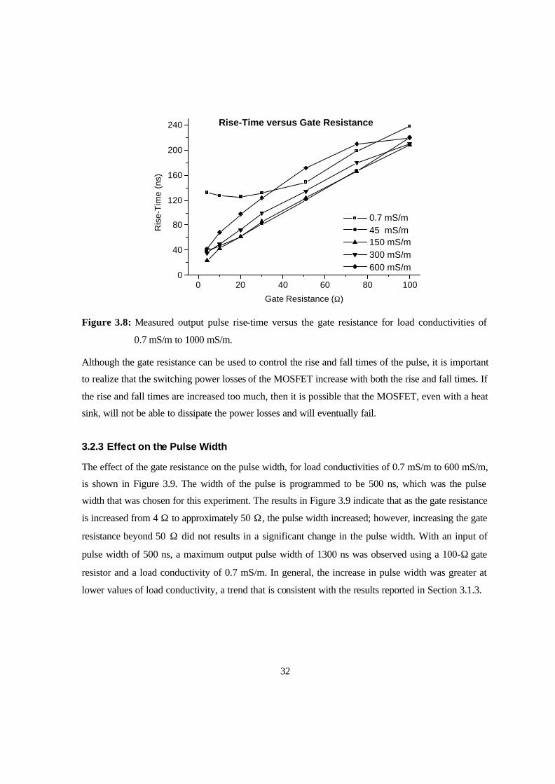
32
0 20 40 60 80 1000
40
80
120
160
200
240 Rise-Time versus Gate Resistance
0.7 mS/m 45 mS/m 150 mS/m 300 mS/m 600 mS/m
Ris
e-T
ime
(ns)
Gate Resistance (Ω)
Figure 3.8: Measured output pulse rise-time versus the gate resistance for load conductivities of
0.7 mS/m to 1000 mS/m.
Although the gate resistance can be used to control the rise and fall times of the pulse, it is important
to realize that the switching power losses of the MOSFET increase with both the rise and fall times. If
the rise and fall times are increased too much, then it is possible that the MOSFET, even with a heat
sink, will not be able to dissipate the power losses and will eventually fail.
3.2.3 Effect on the Pulse Width
The effect of the gate resistance on the pulse width, for load conductivities of 0.7 mS/m to 600 mS/m,
is shown in Figure 3.9. The width of the pulse is programmed to be 500 ns, which was the pulse
width that was chosen for this experiment. The results in Figure 3.9 indicate that as the gate resistance
is increased from 4 Ω to approximately 50 Ω, the pulse width increased; however, increasing the gate
resistance beyond 50 Ω did not results in a significant change in the pulse width. With an input of
pulse width of 500 ns, a maximum output pulse width of 1300 ns was observed using a 100-Ω gate
resistor and a load conductivity of 0.7 mS/m. In general, the increase in pulse width was greater at
lower values of load conductivity, a trend that is consistent with the results reported in Section 3.1.3.

33
0 20 40 60 80 100400
600
800
1000
1200
1400Pulse Width versus Gate Resistance
0.7 mS/m 45 mS/m 150 mS/m 300 mS/m 600 mS/m
Pul
se W
idth
(ns
)
Gate Resistance (Ω)
Figure 3.9: Measured output pulse width versus the gate resistance for load conductivities of
0.7 mS/m to 1000 mS/m.
With the controllability implemented in the power and control module, obtaining the desired output
pulse width can be achieved by adjusting the width of the output pulse of the microcontroller, to
compensate for any difference due to the load conductivity.
3.3 Varying the Energy Storage Capacitance
The capacitance of the energy storage capacitor is an important parameter as it determines the
amount of charge that the capacitor can hold and the amount of time it takes to acquire that charge.
As it turns out, the capacitance of the energy storage capacitor can influenc e the pulse amplitude, rise
and fall times, and pulse width. To study the effect of the energy storage capacitance on these pulse
parameters, the control module was programmed to output a 20-µs pulse, the high-voltage source was
set to supply 500 V, and the capacitance was varied from 100 nF to 15 µF. For each value of
capacitance, the conductivity of the load was varied from 0.7 mS/m to 1000 mS/m. Since both the
parallel and series-MOSFET pulsed power supplies used the same energy storage capacitor, and the
differences between the pulsed power supplies were already noted in Section 3.1, these result were
obtained only using the parallel-MOSFET pulsed power supply using only a single MOSFET.

34
3.3.1 Effect on the Pulse Amplitude
The results of varying the energy storage capacitance on the pulse amplitude over a range of load
conductivities of 0.7 mS/m to 1000 mS/m are shown in Figure 3.10. For capacitance values less than
3 µF, the pulse amplitude decreased when the capacitance was decreased, except for the load
conductivity of 0.7 mS/m. The reason is that these capacitances did not have enough energy to sustain
the pulse amplitude for the entire duration of the 20-µs pulse, except for the 0.7-mS/m load
conductivity, where the lower load current would require less energy from the capacitor. If the pulse
width were to be larger than 20 µs, then the minimum value of capacitance required to reach the
maximum amplitude for that specific load conductivity would be greater than 3 µF, because of the
increased energy that would be required. It is important to realize that increasing the capacitance only
increased the voltage amplitude to a certain value depending on the conductivity of the load. The
maximum amplitude values for each value of load conductivity matched those recorded in Figure 3.2,
which were lower than the input voltage because the load resistance then became comparable to the
on-state resistance of the MOSFET.
0 2 4 6 8 10 12 14 16
0
50
100
150
200
250
300
350
400
450
500
Pulse Amplitude versus Capacitance
0.7 mS/m 300 mS/m 45 mS/m 600 mS/m 150 mS/m 1000 mS/m
Pul
se A
mpl
itude
(V)
Capacitance (µF)
Figure 3.10: Measured output voltage amplitude versus energy storage capacitance for load
conductivities of 0.7 mS/m to 1000 mS/m.

35
3.3.2 Effect on the Rise and Fall Times of the Pulse
The effect of the energy storage capacitance on the fall and rise times, for load conductivities of
0.7 mS/m to 1000 mS/m, is shown in Figure 3.11 and Figure 3.12, respectively. In general, as the
load conductivity increased the fall-time increased, indicating that the fall-time is dependent on the
load. This is consistent with the results that were presented in Section 3.1.2. For load conductivities
below 150 mS/m the fall-time was not affected by the energy storage capacitance. However, for load
conductivities of 150 mS/m and above, there are small variations occurring at low values of energy
storage capacitance. As the capacitance is increased beyond 1.5 µF, the fall-time increased slightly.
The effect of the energy storage capacitance on the fall-time is not very significant as the changes
were less than 30 ns and the slowest fall-time recorded was only 80 ns. The pulses produced using
capacitances of 100 nF and 750 nF did not have sufficient energy to produce a perfect square pulse,
which influenced the oscilloscopes measurement of the fall-time.
0 2 4 6 8 10 12 14 16
20
40
60
80
100 Fall-Time versus Capacitance
0.7 mS/m 300 mS/m 45 mS/m 600 mS/m 150 mS/m 1000 mS/m
Fal
l-Tim
e (n
s)
Capacitance (µF) Figure 3.11: Measured fall-time versus energy storage capacitance for load conductivities of 0.7
mS/m to 1000 mS/m.
It is clear from Figure 3.12 that for a load conductivity of 0.7 mS/m, the rise-time is higher than
those for the rest of the load conductivities, which are all close together. The rapid decrease in rise-
time as the load conductivity increases, is consistent with the results presented in Section 3.1.2. For
capacitances less than 1.2 µF, the rise-time varies within 20 ns of its initial value; however, any
further increase in capacitance did not change the rise-time significantly.

36
0 2 4 6 8 10 12 14 1620
40
60
80
100
120
140
160
Rise-Time versus Capacitance
0.7 mS/m 45 mS/m 150 mS/m 300 mS/m 600 mS/m 1000 mS/mR
ise-
Tim
e (n
s)
Capacitance (µF)
Figure 3.12: Measured rise-time versus energy storage capacitance for load conductivities of
0.7 mS/m to1000 mS/m.
3.3.3 Effect on the Pulse Width
The results of varying the energy storage capacitance on the pulse width over a range of load
conductivities from 0.7 mS/m to1000 mS/m are shown in Figure 3.13. The microcontroller was
programmed to output a 20-µs pulse, which is the pulse width that was chosen for this experiment.
The results in Figure 3.13 show that for all values of the load conductivity, a capacitance of 750 nF or
greater was sufficient to maintain the entire 20-µs pulse. When a capacitance of less than 750 nF was
used with a load conductivity greater than 45 mS/m, the pulse width collapsed because there was not
enough energy stored in the capacitor. As the load conductivity decreased, the current required from
the load increased, which required more energy. In general, a larger capacitance is required when the
load conductivity increases. In addition, longer pulses or multiple pulses also require more energy and
thus, a larger capacitance. Reference [14] provides calculations for the amount of energy required by
each pulse and in the case of multiple pulses.
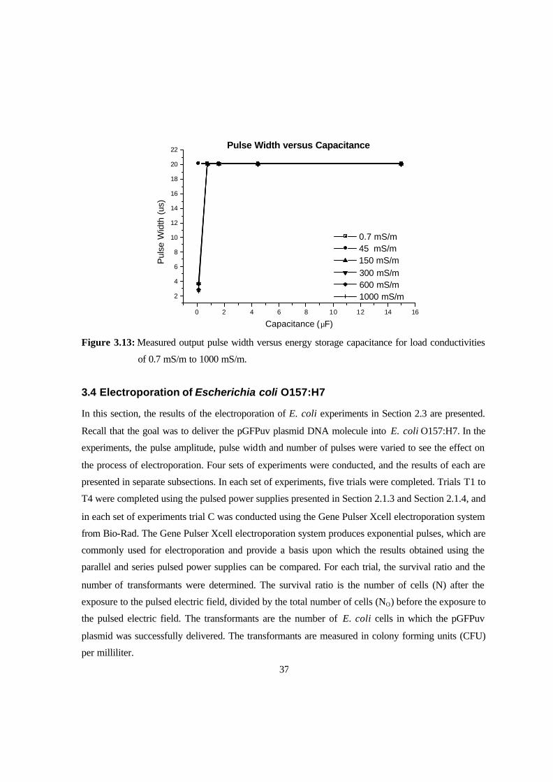
37
0 2 4 6 8 10 12 14 16
2
4
6
8
10
12
14
16
18
20
22 Pulse Width versus Capacitance
0.7 mS/m 45 mS/m 150 mS/m 300 mS/m 600 mS/m 1000 mS/m
Pul
se W
idth
(us
)
Capacitance (µF) Figure 3.13: Measured output pulse width versus energy storage capacitance for load conductivities
of 0.7 mS/m to 1000 mS/m.
3.4 Electroporation of Escherichia coli O157:H7
In this section, the results of the electroporation of E. coli experiments in Section 2.3 are presented.
Recall that the goal was to deliver the pGFPuv plasmid DNA molecule into E. coli O157:H7. In the
experiments, the pulse amplitude, pulse width and number of pulses were varied to see the effect on
the process of electroporation. Four sets of experiments were conducted, and the results of each are
presented in separate subsections. In each set of experiments, five trials were completed. Trials T1 to
T4 were completed using the pulsed power supplies presented in Section 2.1.3 and Section 2.1.4, and
in each set of experiments trial C was conducted using the Gene Pulser Xcell electroporation system
from Bio-Rad. The Gene Pulser Xcell electroporation system produces exponential pulses, which are
commonly used for electroporation and provide a basis upon which the results obtained using the
parallel and series pulsed power supplies can be compared. For each trial, the survival ratio and the
number of transformants were determined. The survival ratio is the number of cells (N) after the
exposure to the pulsed electric field, divided by the total number of cells (NO) before the exposure to
the pulsed electric field. The transformants are the number of E. coli cells in which the pGFPuv
plasmid was successfully delivered. The transformants are measured in colony forming units (CFU)
per milliliter.

38
3.4.1 Experiment #1: Two 1.35-MV/m Microsecond Pulses
In the first of four experiments, two 1.35-MV/m square pulses separated by 80 µs were applied to an
electroporation cuvette containing the cell suspension and plasmid DNA. In the trials T1 to T4, the
parallel-MOSFET pulsed power supply was used to generate pulses of increasing widths to see the
effect on the electroporation process. In trial C, the Gene Pulser system was used to deliver an
exponential pulse with the same field strength but a much longer width than those produced by
parallel-MOSFET pulsed power supply. The results of the five trials are presented in Table 3.1.
Table 3.1: Results of the first set of electroporation experiments to study the effect of increasing the
pulse width of two 1.35-MV/m pulses on the survival ratio and number of transformants
Trial
Pulse Width
(µs)
Electric Field
Strength (MV/m)
Survial Ratio
(N/NO)
Transformants
(CFU/ml)
T1 1 1.35 0.916 0
T2 10 1.36 0.991 0
T3 25 1.26 0.997 0
T4 50 1.22 0.805 0
C 5100* 1.39 0.424 800000
* indicates that the measurement is the time constant of an exponential pulse
The four trails were not successful in transforming any of the cells as indicated in Table 3.1.
However, the much longer exponential pulse produced by the Gene Pulser was successful in
transforming the cells, providing the hint that longer pulses should be used. The initial cell
concentration (NO) in this experiment was 3.75x10¹⁰ CFU/ml and only 800000 CFU/ml were
transformed. It is also interesting to note that when the cells were successfully transformed, the
number of surviving cells had decreased to 0.424 of the initial population.
3.4.2 Experiment #2: Multiple 1.35-MV/m Microsecond Pulses
The second set of experiments consisted of four trials, T1 to T4, using the parallel-MOSFET pulsed
power supply and one trial, C, using the Gene Pulser. In an attempt to test a different strategy, T1
used 255, 1.35-MV/m, 1-µs square pulses each separated by 3 µs. Trials T2 to T4 used two

39
increasingly longer 1.35-MV/m square pulses separated by 600 µs. Trial C used a single exponential
pulse with a time constant of 5 ms. The selective plates showing the number of transformants and the
non-selective plates showing the number of surviving cells for each trial are shown in Figure 3.14 and
Figure 3.15, respectively. The plates give visual comparison of the results; however, the actual
number of transformants and surviving cells for each trial are available in Table 3.2.
T1 T2 T3 T4 C
Figure 3.14: Selective plates showing the cells that have been transformed. The samples that were
plated have been diluted 10 times.
T1 T2 T3 T4 C
Figure 3.15: Non-selective plates showing the total number of surviving cells. The samples that were
plated have been diluted 108 times.
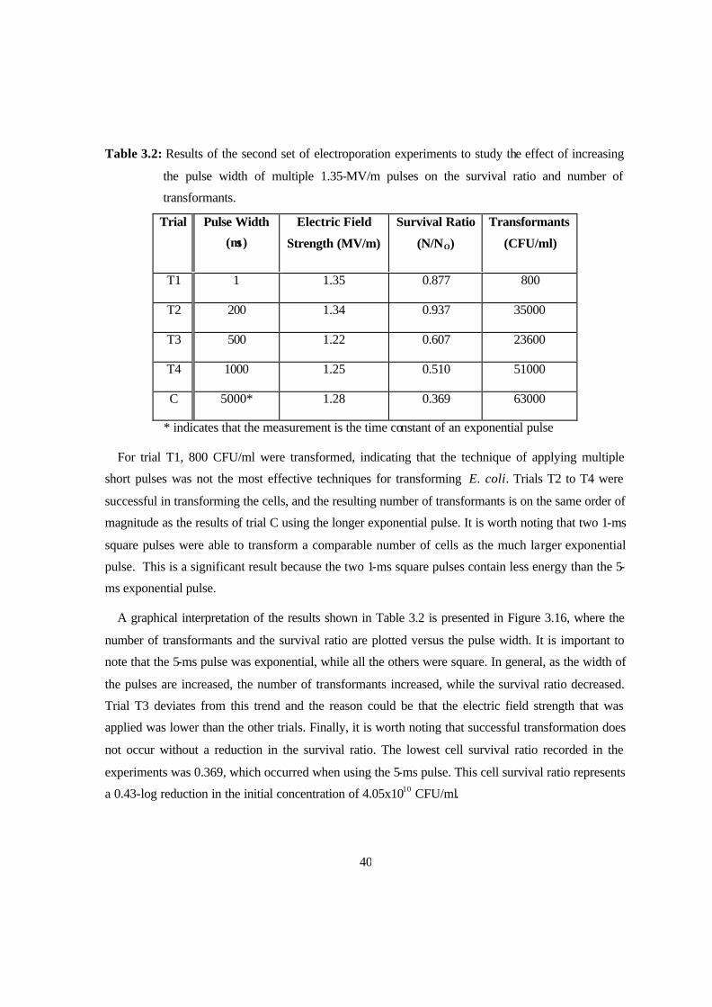
40
Table 3.2: Results of the second set of electroporation experiments to study the effect of increasing
the pulse width of multiple 1.35-MV/m pulses on the survival ratio and number of
transformants.
Trial
Pulse Width
(µs)
Electric Field
Strength (MV/m)
Survival Ratio
(N/NO)
Transformants
(CFU/ml)
T1 1 1.35 0.877 800
T2 200 1.34 0.937 35000
T3 500 1.22 0.607 23600
T4 1000 1.25 0.510 51000
C 5000* 1.28 0.369 63000
* indicates that the measurement is the time constant of an exponential pulse
For trial T1, 800 CFU/ml were transformed, indicating that the technique of applying multiple
short pulses was not the most effective techniques for transforming E. coli. Trials T2 to T4 were
successful in transforming the cells, and the resulting number of transformants is on the same order of
magnitude as the results of trial C using the longer exponential pulse. It is worth noting that two 1-ms
square pulses were able to transform a comparable number of cells as the much larger exponential
pulse. This is a significant result because the two 1-ms square pulses contain less energy than the 5-
ms exponential pulse.
A graphical interpretation of the results shown in Table 3.2 is presented in Figure 3.16, where the
number of transformants and the survival ratio are plotted versus the pulse width. It is important to
note that the 5-ms pulse was exponential, while all the others were square. In general, as the width of
the pulses are increased, the number of transformants increased, while the survival ratio decreased.
Trial T3 deviates from this trend and the reason could be that the electric field strength that was
applied was lower than the other trials. Finally, it is worth noting that successful transformation does
not occur without a reduction in the survival ratio. The lowest cell survival ratio recorded in the
experiments was 0.369, which occurred when using the 5-ms pulse. This cell survival ratio represents
a 0.43-log reduction in the initial concentration of 4.05x10¹⁰ CFU/ml.

41
0 1000 2000 3000 4000 500020
30
40
50
60
70
Transformants
Tra
nsfo
rman
ts (
103 C
FU
/ml)
Pulse Width (µs)
0.3
0.4
0.5
0.6
0.7
0.8
0.9
1.0Effect of Pulse Width on Electroporation
Sur
viva
l Rat
io (
N/N
O)
Survival Ratio
Figure 3.16: The effect of increasing the pulse width of multiple 1.35-MV/m pulses on the cell
survival ratio and number of transformants.
3.4.3 Experiment #3: Single 2.15-MV/m Microsecond Pulses
In the third set of experiments, the applied electric field strength was increased to 2.15-MV/m by
using the series-MOSFET pulsed power supply described in Section 2.1.4. In trials T1 to T4, a single
square pulse, of increasing pulse width, was used. Trial C used a single 5-ms exponential pulse from
the Gene Pulser. The selective plates showing the number of transformants, and the non-selective
plates showing the number of surviving cells for each trial are shown in Figure 3.17 and Figure 3.18,
respectively. The plates give visual comparison of the results; however, the actual number of
transformants and surviving cells for each trial are available in Table 3.3.

42
T1 T2 T3 T4 C
Figure 3.17: Selective plates showing the cells that have been transformed. The samples that were
plated have been diluted 102 times.
T1 T2 T3 T4 C
Figure 3.18: Non-selective plates showing the total number of surviving cells. The samples that were
plated have been diluted 107 times.
Table 3.3: Results of the third set of electroporation experiments to study the effect of increasing the
pulse width of a single 2.15-MV/m pulses on the cell survival ratio and number of
transformants.
Trial
Pulse Width
(µs)
Electric Field
Strength (MV/m)
Survival Ratio
(N/NO)
Transformants
(CFU/ml)
T1 100 2.18 0.613 3000
T2 200 2.18 0.331 14500
T3 500 2.15 0.227 77500
T4 1000 2.16 0.260 152500
C 4900* 2.12 0.118 720000
* indicates that the measurement is the time constant of an exponential pulse

43
The results indicate that all five of the trials successfully produced transformed cells. A graphical
interpretation of the results presented in Table 3.3 is presented in Figure 3.19, where the number of
transformants and the survival ratio are plotted versus the pulse width. It is important to note that the
5-ms pulse was exponential while all the others were square. From Figure 3.19, it is clear that the
number of transformants increased linearly as the pulse width was inc reased in the range of 100 µs to
5 ms. As the pulse width is increased within the same range, the survival ratio decreased to a
minimum value of 0.118 (0.93-log reduction) occurring at 5 ms. As in the second set of experiments,
a higher number of transformants was accompanied by a lower number of surviving cells. The initial
cell concentration of the samples in this set of experiments was 2.47x10¹⁰ CFU/ml.
0 1000 2000 3000 4000 5000
0
10
20
30
40
50
60
70
80
Sur
viva
l Rat
io (
N/N
O)
Transformants
Tra
nsfo
rman
ts (
104 C
FU
/ml)
Pulse Width (µs)
0.1
0.2
0.3
0.4
0.5
0.6
0.7Effect of Pulse Width on Electroporation
Survival Ratio
Figure 3.19: The effect of increasing the pulse width of a single 2.15-MV/m pulse on the survival
ratio and number of transformants.
3.4.4 Experiment #4: Increasing the Number of 2.15-MV/m, 1-ms Pulses
In the fourth and final set of experiments, the series-MOSFET pulsed power supply was used to
apply multiple 1-ms, 2.15-MV/m pulses across the electroporation cuvette. In trials T1 to T4, the
number of pulses used was increased from one to one-hundred, with 100 ms between each pulse in
order to allow the capacitor to fully recharge. In trial C, the Gene Pulser was used to generate a single
1-ms exponential pulse with a peak electric field strength of 2.15 MV/m. The selective plates showing
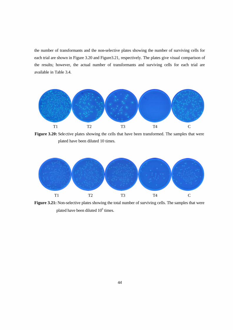
44
the number of transformants and the non-selective plates showing the number of surviving cells for
each trial are shown in Figure 3.20 and Figure3.21, respectively. The plates give visual comparison of
the results; however, the actual number of transformants and surviving cells for each trial are
available in Table 3.4.
T1 T2 T3 T4 C
Figure 3.20: Selective plates showing the cells that have been transformed. The samples that were
plated have been diluted 10 times.
T1 T2 T3 T4 C
Figure 3.21: Non-selective plates showing the total number of surviving cells. The samples that were
plated have been diluted 106 times.

45
Table 3.4: Results of the fourth set of electroporation experiments to study the effect of the number
of 1-ms, 2.15-MV/m pulses on the survival ratio and number of transformants
Trial Number
of Pulses
Electric Field
Strength (MV/m)
Survival Ratio
(N/NO)
Transformants
(CFU/ml)
T1 1 2.15 0.231 70500
T2 5 2.15 0.127 9600
T3 10 2.15 0.135 4050
T4 100 2.15 0.01744 0
C 1* 2.15 0.253 18000
* indicates that the measurement is the time constant of an exponential pulse
For the first time in these experiments, there exists a square and an exponential pulse of
comparable durations and amplitudes. In trial T1, a single 1-ms square pulse was used and in trial C a
single 1-ms exponential pulse was used. The results show that the 1-ms square pulse is approximately
4 times more effective in transforming cells than a 1-ms exponential pulse. However, it should be
noted that the survival ratio of the two pulses remained relatively similar at 0.231 and 0.253 for the
square and exponential pulse respectively.
In trial T4, during the application of the 100 pulses, it was observed that the pulse amplitude started
to decrease after approximately 30 pulses. This decrease in pulse amplitude is not due to insufficient
energy stored in the capacitor because the time between two successive pulses was 100 ms. This time
is more than five time constants of the RC charging circuit, which would allow the capacitor to fully
recharge. A possible explanation for this observation is an increase in conductivity due to the contents
of the cell being exposed after the exposure to a pulsed electric field. Recall from Section 3.1.1 that
an increase in medium conductivity resulted in a decrease in pulse amplitude. An increase in
conductivity of a cell suspension medium immediately after applying a pulsed electric field was
reported in [32].
A graphical interpretation of the results presented in Table 3.4 is presented in Figure 3.22, where
the number of transformants and the survival ratio are plotted versus the pulse width. The results in
Table 3.4 show two trials, trial T1 and trial C, which applied a single pulse. Since only one of those
data points was needed in Figure 3.22, Trial C was omitted. From Figure 3.22 it is clear that the

46
number of transformants and the survival ratio decreased as the number of pulses were increased. The
results indicate that using multiple pulses is not the correct approach when trying to improve the
number of transformants. When 100 pulses were applied, there were no transformants and the
survival ratio was decreased by two orders of magnitude to 0.0174 (1.76–log reduction), where the
initial cell concentration was 1.58x10¹⁰ CFU/ml.
0 20 40 60 80 100
0
10
20
30
40
50
60
70
80 Transformants
Tra
nsfo
rman
ts (1
03 CF
U/m
l)
Number of Pulses
0.00
0.05
0.10
0.15
0.20
0.25
Sur
viva
l Rat
io (
N/N
O)
Effect of Number of Pulses on Electroporation
Survival Ratio
Figure 3.22: Graph showing the effect of increasing the pulse width of 1-ms, 2.15-MV/m pulses on
the survival ratio and number of transformants.

47
Chapter 4
Discussion
In this chapter, the results presented in Chapter 3 are used as a basis for discussion. Based on the
results, five topics are identified and discussed in this chapter. The first section is a discussion on
using the pulsed power supplies with conductive loads, as in many applications the load conductivity
is not a parameter that can be controlled. This leads to a discussion on using MOSFETs in parallel to
reduce the loading effect experienced with loads that are highly conductive. The next two sections
discuss the effects of and how to choose a gate resistance and an energy storage capacitor, both of
which are important circuit parameters of the pulsed power supply. The last section focuses on the
factors that influence the electroporation-mediated plasmid DNA molecule delivery and how to
improve the process. In these sections, the results are explained in detail and whenever possible,
compared to similar studies reported in the literature. In addition, the results of this research are
applied to explain the results and trends that have been published in the literature.
4.1 Using Pulsed Power Supplies With Conductive Loads
In certain applications, mainly in-vitro laboratory experiments, the load conductivity can be
controlled and varied; however, for in-vivo or food processing applications, the load conductivity
depends on the actual treatment media. Factors, including the load conductivity, can influence the
pulse parameters, which several studies have shown to have a significant effect on the process of
opening the pores in the electroporation process. The range of conductivities used in these
experiments cover many of those that are used in electroporation experiments. In addition, it also
covers other applications of pulsed electric field including non-thermal pasteurization of liquid foods
such as tap water, apple juice, and orange juice, whose conductivities are within this range [33].
The load conductivity had an effect on the amplitude of the pulse produced by both of the
MOSFET-based pulsed power supplies. According to the results presented in Section 3.1.1, an
increase in conductivity resulted in a decrease in voltage amplitude, meaning that the electric field
strength would be reduced. Figure 4.1 illustrates this effect by showing two pulses where the only
parameter that changed was the load conductivity. The pulse that was measured across the load with a
conductivity of 0.7 mS/m (de-ionized water), shows no noticeable reduction in amplitude; however,

48
when the load conductivity is increased to 1000 mS/m, the maximum amplitude that was sustained
for the entire duration of the pulse was 196 V.
(A) (B)
Figure 4.1: Measured output voltage pulse from a single MOSFET pulsed power supply with a load
conductivity of (A): 0.7 mS/m and (B): 1000 mS/m
The reduction in amplitude is due to the increased voltage drop across the on-state resistance of the
MOSFET switch. According to (2.5), increasing the load conductivity reduces the resistance of the
load, making it more comparable to the on-state resistance of the MOSFET (5.5 Ω). As a result, a
smaller portion of the total voltage will appear across the load.
The effects of high load conductivity on the parameters of the pulses generated by the MOSFET-
based pulsed power supplies are expected. In fact, they are consistent with the simulation and
experimental results of two earlier prototypes of the MOSFET-based pulsed power supplies that were
designed and built [34,35]. In addition, the results are comparable to those using a Thyratron-based
pulsed power supply that was investigated in [35], and compared to the MOSFET-based pulsed power
supply. The pulsed power supply that used two MOSFETs in series, had the largest reduction in
amplitude as the conductivity was increased. Using two MOSFETs in series doubles the effective on-
state resistance as the two on-state resistances in series are added together.
Commercially available electroporation devices also experience the reduction in pulse amplitude
with increasing conductivity. Figure 4.2, shows the results from Section 3.1.1 with the results of the
Gene Pulser manufactured by Bio-Rad. Since the Gene Pulser produces exponential pulses, the peak
voltage was recorded for a comparison. The Gene Pulser experienced a similar decrease in amplitude
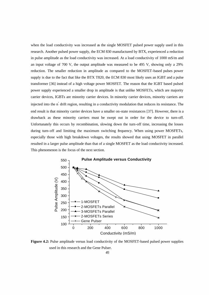
49
when the load conductivity was increased as the single MOSFET pulsed power supply used in this
research. Another pulsed power supply, the ECM 830 manufactured by BTX, experienced a reduction
in pulse amplitude as the load conductivity was increased. At a load conductivity of 1000 mS/m and
an input voltage of 700 V, the output amplitude was measured to be 495 V, showing only a 29%
reduction. The smaller reduction in amplitude as compared to the MOSFET-based pulses power
supply is due to the fact that like the BTX T820, the ECM 830 most likely uses an IGBT and a pulse
transformer [36] instead of a high voltage power MOSFET. The reason that the IGBT based pulsed
power supply experienced a smaller drop in amplitude is that unlike MOSFETs, which are majority
carrier devices, IGBTs are minority carrier devices. In minority carrier devices, minority carriers are
injected into the n- drift region, resulting in a conductivity modulation that reduces its resistance. The
end result is that minority carrier devices have a smaller on-state resistances [37]. However, there is a
drawback as these minority carriers must be swept out in order for the device to turn-off.
Unfortunately this occurs by recombination, slowing down the turn-off time, increasing the losses
during turn-off and limiting the maximum switching frequency. When using power MOSFETs,
especially those with high breakdown voltages, the results showed that using MOSFET in parallel
resulted in a larger pulse amplitude than that of a single MOSFET as the load conductivity increased.
This phenomenon is the focus of the next section.
0 200 400 600 800 1000100
150
200
250
300
350
400
450
500
550 Pulse Amplitude versus Conductivity
1-MOSFET 2-MOSFETs Parallel 3-MOSFETs Parallel 2-MOSFETs Series Gene Pulser
Pul
se A
mpl
itude
(V
)
Conductivity (mS/m)
Figure 4.2: Pulse amplitude versus load conductivity of the MOSFET-based pulsed power supplies
used in this research and the Gene Pulser.

50
Increasing the load conductivity also had an effect on the rise and fall times of the pulse. According
to the results presented in Figure 3.3, as the load conductivity increased the fall-time of the parallel
and the series pulsed power supplies increased as well. For the single MOSFET pulsed power supply,
the fall-time increased from 17 ns to 54 ns when the load conductivity was changed from 0.7 mS/m to
1000 mS/m. This trend is consistent with those that were reported in [14,18]. As the load became
more conductive, the load current increased. The increase in the load current increases the current
rise-time (tri), the time required for the MOSFET drain current to reach the value of the load current,
resulting in a longer fall-time. The fall-time of the pulse determines the time it takes for the pulse to
reach its peak value. A slower fall-time will also delay the development of the transmembrane
potential, which is essential for the opening of the pores in the process of electroporation.
The rise-time of the pulse is also influenced by the load conductivity. For load conductivities below
200 mS/m, an increase in conductivity resulted in a rapid decrease in rise-time. However, the rise-
time did not change significantly for an increase in conductivity above 200 mS/m. When the load
conductivity is small, the load resistance is high and the resulting load current is small. This is similar
to not loading the generator. Notice that the rise-time varies inversely with the conductivity and recall
from (2.5), that the resistance of the load was inversely proportional to the load conductivity. A fast
rise-time is important in order for smaller pulse widths and higher switching frequencies to be
achieved.
Since the conductivity of the load influences many of the important pulse parameters, it is
important to know the load conductivity being used and to measure the pulse to ensure that the pulse
parameters are known exactly. An understanding of the abovementioned results can be applied to the
results reported in the literature. For example, to inactivate microorganisms, the applied electric field
must exceed the threshold electric field for membrane destruction, which is specific to the type of
microorganism [38]. In addition, several studies [39-43] concluded that increasing the electric field
strength is an effective technique to decrease the cell survival ratio. However, if the microorganisms
are suspended in a medium of high conductivity, the input voltage must be increased to compensate
for the reduction in electric field strength. It is important for studies that investigate the effect of
medium conductivity on the transformation efficiency or survival ratio, to take into account the
effects the medium conductivity has on the pulse. For example, if the reduction in field strength at
higher load conductivities is not accounted for, then any effect of the conductivity on the cell itself
cannot be properly observed. As for the fall-time of the pulse, one study concluded that there was no

51
significant dependence of the survival ratio of Yersinia enterocolitica cells on the fall-time in the
range of 500 ns to 1300 ns [40]. However, providing fast fall-times is important for applications such
as electroperturbation, which require pulses of nanosecond widths [44].
4.2 Paralleling MOSFETs to Reduce the Loading Effect
According to Figure 4.2, an increase in the load conductivity resulted in a decrease in voltage
amplitude, meaning that the electric field strength would be reduced. For a load conductivity of 1000
mS/m, using two and three MOSFETs in parallel increased the pulse amplitude by 17% and 28% over
the value obtained using only a single MOSFET, respectively. To understand why the output voltage
is improved as a result of using a higher number of MOSFETs in parallel, it is necessary to recall why
the output voltage amplitude decreases with loads of higher conductivity. According to (2.5),
increasing the conductivity reduces the resistance of the load and as a result, the load current
increases proportionally. A larger load current causes a larger voltage drop across the MOSFET’s on-
state resis tance (5.5 Ω), leaving less voltage to appear across the load. By paralleling MOSFETs, the
equivalent on-state resistance decreases. This results in a smaller voltage drop across the switch,
which allows more voltage to appear across the load. Since a single MOSFET driver was used to
drive the parallel MOSFETs, an increase in fall-time is expected and observed because the effective
input capacitance of the paralleled MOSFET has increased two or three times. However, these turn-
on times remain smaller than many single IGBTs of comparable voltage ratings. In general, using
MOSFETs in parallel to reduce the effective on-state resistance is an especially useful technique
when using power MOSFETs with high breakdown voltages because of their high on-state
resistances. For power MOSFETs, experimental results and detailed theoretical calculations reveal
that the on-state resistance varies with the breakdown voltage, VB, as follows [24]:
7.25.2)(
−BonDS VR α (4.1)
The increase in amplitude achieved by using MOSFETs in parallel is of practical significance.
Higher voltage amplitude results in higher electric field strength, which is a key parameter for
successful electroporation-mediated applications.

52
4.3 Varying the Gate Resistance to Control the Rise and Fall Times of the
Pulse
The gate resistance controls the amount of current that flows into and out of the gate when the
MOSFET switches on and off, which controls the MOSFET’s turn-on and turn-off times. Increasing
the gate resistance in the range of 4 Ω to100 Ω, resulted in a linear increase in the fall and rise times
of the output pulse, as shown in Figure 3.7 and Figure 3.8, respectively. This is the expected result as
a larger resistance results in a slower charging and discharging of the MOSFET’s input capacitance.
To understand the turn-on and turn-off process, Figure 4.3 illustrates the gate-source voltage before
and after the 4-Ω-gate resistor, and the difference between the two, which is proportional to the gate
current. The gate-source voltage contains several different stages to completely turn-on the MOSFET.
Understanding these stages helps to explain the resulting increase in rise and fall times of the output
pulse as the gate resistance increased. The first stage (up to t1) is the time required to bring the gate-
source voltage to its threshold value. From t1 to t2 the gate -source and gate drain capacitances are
being charged through the gate resistance. At t2, the drain-source voltage starts to fall, which
introduces the miller effect. The gate-source voltage does not increase until the gate current has fully
charged the miller capacitance (t3), hence the plateau in the gate -source voltage. The final stage (t3 to
t4) is to fully enhance the MOSFET by increasing the gate-source voltage to the value of the drive
voltage, which also reduces the on-state resistance. With a larger gate resistance, the charging of the
capacitances is slower, thereby increasing the fall-time of the pulse.
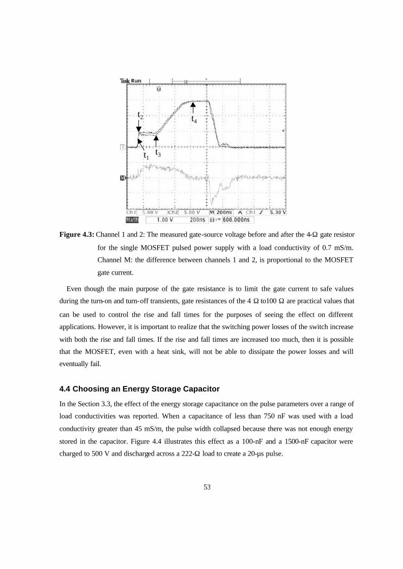
53
Figure 4.3: Channel 1 and 2: The measured gate-source voltage before and after the 4-Ω gate resistor
for the single MOSFET pulsed power supply with a load conductivity of 0.7 mS/m.
Channel M: the difference between channels 1 and 2, is proportional to the MOSFET
gate current.
Even though the main purpose of the gate resistance is to limit the gate current to safe values
during the turn-on and turn-off transients, gate resistances of the 4 Ω to100 Ω are practical values that
can be used to control the rise and fall times for the purposes of seeing the effect on different
applications. However, it is important to realize that the switching power losses of the switch increase
with both the rise and fall times. If the rise and fall times are increased too much, then it is possible
that the MOSFET, even with a heat sink, will not be able to dissipate the power losses and will
eventually fail.
4.4 Choosing an Energy Storage Capacitor
In the Section 3.3, the effect of the energy storage capacitance on the pulse parameters over a range of
load conductivities was reported. When a capacitance of less than 750 nF was used with a load
conductivity greater than 45 mS/m, the pulse width collapsed because there was not enough energy
stored in the capacitor. Figure 4.4 illustrates this effect as a 100-nF and a 1500-nF capacitor were
charged to 500 V and discharged across a 222-Ω load to create a 20-µs pulse.
t2 t4
t3 t1
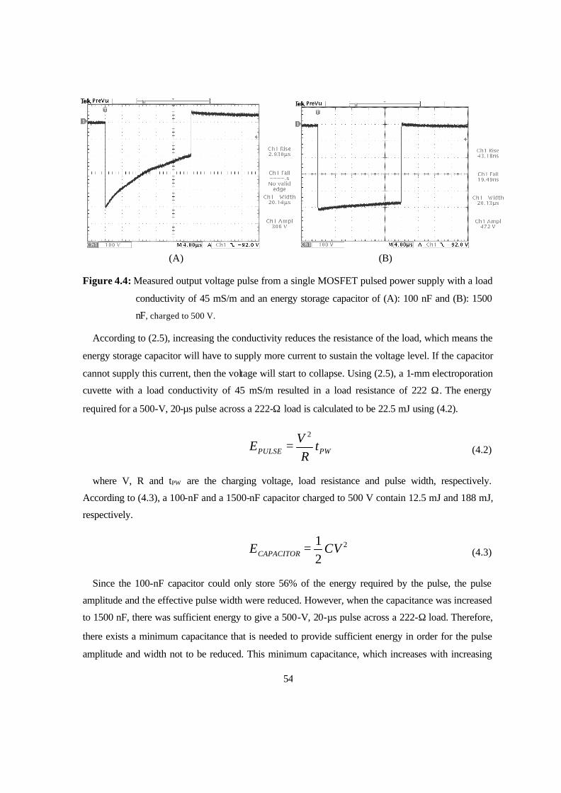
54
(A) (B)
Figure 4.4: Measured output voltage pulse from a single MOSFET pulsed power supply with a load
conductivity of 45 mS/m and an energy storage capacitor of (A): 100 nF and (B): 1500
nF, charged to 500 V.
According to (2.5), increasing the conductivity reduces the resistance of the load, which means the
energy storage capacitor will have to supply more current to sustain the voltage level. If the capacitor
cannot supply this current, then the voltage will start to collapse. Using (2.5), a 1-mm electroporation
cuvette with a load conductivity of 45 mS/m resulted in a load resistance of 222 Ω. The energy
required for a 500-V, 20-µs pulse across a 222-Ω load is calculated to be 22.5 mJ using (4.2).
PWPULSE tR
VE2
= (4.2)
where V, R and tPW are the charging voltage, load resistance and pulse width, respectively.
According to (4.3), a 100-nF and a 1500-nF capacitor charged to 500 V contain 12.5 mJ and 188 mJ,
respectively.
2
21 CVECAPACITOR = (4.3)
Since the 100-nF capacitor could only store 56% of the energy required by the pulse, the pulse
amplitude and the effective pulse width were reduced. However, when the capacitance was increased
to 1500 nF, there was sufficient energy to give a 500-V, 20-µs pulse across a 222-Ω load. Therefore,
there exists a minimum capacitance that is needed to provide sufficient energy in order for the pulse
amplitude and width not to be reduced. This minimum capacitance, which increases with increasing

55
pulse width and decreasing load resistance, can be obtained by equating (4.2) to (4.3). A capacitor
that is larger than the minimum value should be used in order to compensate for losses in the circuit,
particularly with loads of high conductivity.
In applications, such as inactivation of microorganisms in food processing where the load must
flow continuously, the ability to deliver multiple pulses is essential. The use of multiple pulses has
been used to increase the inactivation of microorganisms [15]. If multiple pulses are required, then the
capacitor must store sufficient energy for all of the pulses or allow sufficient time (5 time constants)
between the application of two successive pulses in order to recharge the capacitor. Choosing a
capacitor for these applications requires a tradeoff between the amount of energy the capacitor can
store versus how much time it takes for it to become fully charged. Larger capacitors are typically
larger in size, more costly, result in higher losses, and are more difficult to obtain at higher voltage
ratings.
4.5 Improving Electroporation-Mediated Plasma DNA molecule Delivery
This section discusses the results of the four electroporation experiments presented in Section 3.4.
The goal was to deliver the pGFPuv plasmid DNA molecule into E. coli O157:H7. In addition to
increasing the pulse width and number of pulses, which are discussed in separate sub-sections, there
are some important observations that are discussed.
In the first three experiments, it is interesting to note that successful transformation of E. coli was
accompanied by a reduction in the survival ratio in the range of 0.118 to 0.937, with more
transformants occurring when the survival ratio was lower. This would suggest that the lower number
of transformants is not due to a high number of cells being inactivated, but that there was not enough
energy to make the cell membrane permeable. In the fourth experiment, when multiple pulses were
applied to the cuvette, the transformation of E. coli was accompanied by a reduction in the survival
ratio in the range of 0.0174 to 0.253, with more transformants occurring when the survival ratio was
higher. In this case, it appears that the lower number of transformants could be due to the number of
cells that were inactivated. However, this assumes that there are no other effects due to the
application of multiple pulses, as this is how the higher reduction in survival ratio was achieved.
In the fourth experiment there exists a square and an exponential pulse of similar durations and
amplitudes, which are compared. In trial T1, a single 1-ms square pulse was used and in trial C, a
single 1-ms exponential pulse was employed. The results show that the 1-ms square pulse yielded

56
approximately 4 times more transformants than the 1-ms exponential pulse with the same amplitude.
One possible explanation for the improvement in the number of transformants with the square pulse
over the exponential pulse is that the average electric field strength is higher in the square pulse. The
concept of the average electric field strength was used to explain the increased inactivation with
square pulses as compared with exponential pulse [45]. Another study [15] concluded that square
pulses result in 60% more inactivation than exponential pulse with the same energy.
The electric field strength to which the cells are exposed is critical to the resulting number of
transformants and survival ratio. When the field strength of a 5-ms exponential pulse was increased
from 1.28 MV/m to 2.12 MV/m, the number of cells in the initial population that were transformed
was increased from 1 in 642,857 to 1 in 34,305. However, this comparison was between two different
sets of experiments. This is normally not done because there are many conditions such as
temperature, length of time at the different stages of the experiments, and the growth phase of the
cells that could vary during the two experiments. However, in these experiments the same procedures,
solutions and bacterial cells were used and the difference between the results is significant enough to
make this observation with less risk of error. The effects of an increase in electric field strength are
available in the literature and they do support the observation made between these experiments. One
study [43], reported that the transformation efficiency of E. coli JM109 reached a maximum at a field
strength of 1.7 MV/m then decreased with any further increase in electric field strength. The same
trend of increased transformation efficiency up to certain electric field strength was also reported in
[46,47]. An increase in electric field strength results in a decrease in the survival ratio. The survival
ratio of E. coli JM109 decreased as the electric field strength was increased from 1.1 MV/m to 2
MV/m [43] and up to a 6-log reduction in the survival ratio of Lactobacillus brevis by increased
electric field strength was reported in [42].
4.5.1 Effect of Pulse Width on Electroporation
The results of the experiments from Sections 3.4.2 and 3.4.3 show the effect of increasing the pulse
width from 100 µs to 5 ms on the number of transformants and the survival ratio. In both set of
experiments, increasing the pulse width increased the number of transformants and decreased the
survival ratio exponentially. The results presented here on the effect of the pulse width on the number
of transformants are consistent with the results reported in the literature. One study [46] found that
increasing the pulse width of 1.15-MV/m pulses from 2.5 ms to 4.5 ms, results in an increase in the
57
transformation frequency of Candida famata L20105. However, increasing the pulse width beyond
this width up to 7.5 ms, resulted in a decrease in the transformation frequency. The later effect,
showing the number of transformants decreasing as the pulse widths increased, was not observed in
this research because the pulse width was not increased beyond 5 ms. The pulse width determines the
time for which the pulsed electric field will be applied. This is also the time during which the pores in
the cell membrane will form. If the electric field is applied for too long a time, the cell membrane will
be irreversibly damaged. This is one explanation for the decrease in the transformation frequency at
higher pulse widths.
The observed exponential decrease in survival ratio as the pulse width was increased, is consistent
with other results reported in the literature. While studying the effects of pulsed electric fields on
Lactobacillus brevis, it was reported that increasing the pulse width of exponential pulses up to
12 ms, resulted in an exponential decrease in the survival ratio [42]. Another study [39], reported a
decrease in survival ratio of Saccharomyces cerevisiae when the width of square pulses were
increased from 1 µs to 100 µs.
4.5.2 Effect of the Number of Pulses on Electroporation
The experimental results reported in Section 3.4.4 demonstrate the effect of increasing the number
of pulses on the number of transformants and the survival ratio. The results in Figure 3.22 illustrate
that increasing the number of 1-ms, 2.15-MV/m pulses from 1 to 100 resulted in a drastic reduction in
the number of transformants. In fact, when the number of pulses was increased from 1 to 100, the
number of transformants decreased from 70500 to 0. A possible explanation for the reduction in the
number of transformants is the low survival ratio as the number of pulses increased, which is also
illustrated in Figure 3.22. In all of the experiments, successful transformation was accompanied by a
reduction in the survival ratio; however, the survival ratio for multiple pulse were much lower (1.76-
log reduction with 100 pulse) than those resulting from only a single pulse. A similar study [48]
reported a 0.82-log and 4.47-log reduction of E. coli O157:H7 using 50 and 300 5-ms exponential
pulses with field strengths of 2.5 MV/m, respectively. The results showing the number of
transformation decreasing as the number of pulses is increased are consistent with those that were
reported by [49]. Other studie s showed a rapid decrease in the survival ratio of Yersinia enterocolitica
[40] and Saccharomyces cerevisiae [50] as the number of pulses was increased. Therefore it is

58
concluded that using multiple pulses in not effective in increasing the number of transformants;
however, it is a good technique for inactivating microorganisms.
In trial T4 of the fourth experiment, after approximately 30 of the 100 pulses, the amplitude of the
pulses was observed to start decreasing. This decrease in pulse amplitude is not due to insufficient
energy stored in the capacitor because the time between two successive pulses was 100 ms. This time
is more than five time constants of the RC charging circuit, which would allow the capacitor to fully
recharge. Recall from Section 3.1.1 that an increase in load conductivity resulted in a decrease in
pulse amplitude. This could explain the reduction in pulse amplitude as an increase in conductivity of
a cell suspension medium was reported to occur immediately after exposure to a pulsed electric field
[32].

59
Chapter 5
Conclusions and Future Research
5.1 Conclusions
In this research, two MOSFET-based pulsed power supplies that were used in electroporation
experiments, were designed and built. The first pulsed power supply allowed one, two, or three
MOSFETs to be connected in parallel in order to decrease the effective on-state resistance. This
pulsed power supply was capable of producing highly controllable square pulses with amplitudes up
to 1500 V and widths of a few hundred nanoseconds to dc. Due to the voltage limitation of the
MOSFET switch, and the need to produce a stronger electric field, a second pulsed power supply
using two MOSFETs connected in series was designed and built. This pulsed power supply was
capable of producing high ly controllable square pulses with amplitudes up to 3000 V and widths of a
few hundred nanoseconds to dc. Since precise control of the pulse parameters is important for the
applications of pulsed electric fields, especially when it is necessary to optimize a process, a
microcontroller was used. This provided a high degree of control of the pulse width, number of pulses
and the time between two successive pulses. The modular design of the pulsed power supplies
allowed them to use the same power and control module that was built for this purpose.
The effects of varying the load conductivity from 7 mS/m to 1000 mS/m on the output pulse of the
pulsed power supplies were studied. It was observed that an increase in load conductivity resulted in a
decrease in voltage amplitude, resulting in an undesirable reduction in the electric field strength. The
reason for the reduction in amplitude was due to the increased voltage drop across the on-state
resistance of the MOSFET switch. The pulsed power supply that used two MOSFETs in series
experienced the most significant reduction in amplitude, as the effective on-state resistance was
doubled. However, using two and three MOSFETs in parallel at a load conductivity of 1000 mS/m,
increased the pulse amplitude by 17% and 28%, respectively, over the value obtained using only a
single MOSFET. Therefore, it was concluded that using two or three MOSFETs in parallel is an
effective method of increasing the amplitude of the output pulse when working with high load
conductivities. Increasing the load conductivity also had an effect on the rise and fall times of the
pulse. As the load conductivity was increased, the fall-time increased, while the rise-time rapidly
decreased up to a load conductivity of 200 mS/m, where it reached a cons tant value. Since the
conductivity of the load influences many of the important pulse parameters, it is important to know
60
the conductivity of the load being used and to measure the pulse to ensure that the pulse parameters
are known exactly.
The gate resistance and the energy storage capacitance were varied to see the effect on the pulse
parameters. Increasing the gate resistance in the range of 4 Ω to100 Ω resulted in a linear increase in
the rise and fall times of the pulse. Therefore, varying the gate resistance within this range can be
used to adjust the rise and fall times of the pulse for different applications. The energy storage
capacitance determined the amount of energy that can be stored and used to supply one or multiple
pulses. A method for determining the minimum capacitance needed to provide the required energy, in
order for the pulse amplitude and width not to be reduced, was presented. It was concluded that
choosing an energy storage capacitor for an application required a tradeoff between the amount of
energy the capacitor can store versus how much time it takes for it to become fully charged.
In conclusion, the pulse parameters can be controlled by the circuit parameters such as the number
of parallel MOSFETs, gate resistance, energy storage capacitance, and the parameters of the gating
pulses generated by the microcontroller. In this way, the parameters of the output pulse can be made
almost independent of the load conductivity.
The pulsed power supplies that were designed and built in this work were used to investigate the
effect of the pulse parameters on the electroporation-mediated plasmid DNA delivery. The goal was
to deliver a 3.3-kb pGFPuv plasmid DNA molecule into E. coli O157:H7. Two electroporation
experiments were conducted using the parallel-MOSFET pulsed power supply, which applied 1.35-
MV/m square pulses in the range from 1 µs to 1 ms. Two other experiments were conducted using the
series-MOSFET pulsed power supply, which applied 2.15-MV/m pulses with the widths ranging from
100 µs to 1 ms. In all four experiments, the Gene Pulser Xcell system was used to generate
exponential pulses of comparable width and amplitude. From these experiments, it was observed that
increasing the pulse width in the range from 100 µs to 5 ms, increased the number of transformants
and decreased the survival ratio exponentially. When the field strength of a 5-ms exponential pulse
was increased from 1.28 MV/m to 2.12 MV/m, the number of cells in the initial population that were
transformed was increased from 1 in 642 857, to 1 in 34 305. In the first three experiments, it is
interesting to note that the successful transformation of E. coli was accompanied by a reduction in the
survival ratio of at most 1 log. This suggested that the lower number of transformants was due to
insufficient energy to make the cell membrane permeable, and not a high number of cells being
inactivated. However, when multiple pulses were applied, the reduction in survival ratio increased

61
beyond 1 log and the number of transformants was decreased. In this case, it appeared that the lower
number of transformants was due to the high number of cells that were inactivated. Therefore, it is
concluded that using multiple pulses was not effective in increasing the number of transformants;
however, it is an effective technique for inactivating microorganisms. Finally, square pulses were
observed to be more effective in transforming and inactivating cells than exponential pulses of the
same amplitude and pulse width. It was hypothesized that this is due to the higher average field
strength of the square pulse.
5.2 Future Research
The relatively lower voltage ratings of MOSFETs prompted the pulsed power supply to use two
MOSFETs in series, which enabled pulses of 3000 V to be produced. Future work would be to
increase the number of MOSFETs connected in series using the same method, in order to further
increase the amplitude of the output pulses. However, the effective on-state resistance will increase
with the number of MOSFETs connected in series. Therefore, combining the techniques used in this
work to design a pulsed power supply that uses MOSFETs in series and in parallel simultaneously,
will help minimize the effective on-state resistance as the number of series connected MOSFETs
increases.
The number of pulses per second that can be generated is limited by the amount of energy stored in
the capacitor and the amount of time it takes to recharge the capacitor, not by the speed of the
MOSFET. Therefore, using a capacitor charger (cap charger) could increase the number of pulses per
second that can be generated.
Since the pulsed power supplies in this work have a high degree of control over the rise and fall
times of the pulses, pulse width, number of pulses, and the time between two successive pulses, future
research could be conducted on other applications needing pulsed electric fields. Applications
involving the continuous flow of highly conductive fluids could benefit from the pulsed power
supplies in this research.
62
References
[1] E. Neumann, A.E. Sowers, and C.A. Jordan, Electroporation and Electrofusion in Cell Biology. Plenum Press, New York, 1989.
[2] U. Zimmermann, “Electrical Breakdown, Electropermeabilization and Electrofusion,” Rev. Physiol. Biochem. Pharmacol. Vol. 105, pp. 176-250, 1986.
[3]. A. Barnett and J.C. Weaver, “Electroporation: A unified quantitative theory of reversible electrical breakdown and mechanical rupture in artificial planar bilayer membranes,” Bioelectrochemistry and Bioenergetics, 25(1991), pp. 163-182.
[4] J.C. Weaver and Y. A. Chizmadzhev, “Theory of electroporation: A review,” Bioelectrochemistry and Bioenergetics, Vol. 41, 1996, pp. 135-160.
[5] T.F. Wu, S.Y. Tseng, D.C. Su, Y.M. Chen, and Y.K. Chen, “Applications of soft-switching full-bridge converter and rotational electric field to transdermal drug delivery,” Nineteenth Annual IEEE Applied Power Electronics Conference and Exposition, Vol. 2, 2004, pp. 919-925.
[6] U. Zimmermann, “Electrical breakdown, electropermeabilization and electrofusion,” Rev. Physicol. Biochem. Pharmacol. Vol. 105, pp. 75-256, 1986.
[7] T. Grahl and H. Markl, “Killing of microorganisms by pulsed electric fields,” Appl. Microbio. Biotechnol., 45, pp. 148-157, 1996.
[8] K.H. Schoenbach, S. Katsuki, R. Stark, E.S. Buescher, and S.J. Beebe, “Bioelectrics-New Applications for Pulsed Power Technology,” IEEE Trans. Plasma Science, vol. 30, no. 1, Feb. 2002, pp. 293-300.
[9] S.B. Dev, D.P. Rabussay, G. Widera, and G.A. Hoffmann, “Medical Applications of Electroporation,” IEEE Trans. Plasma Science, vol. 28, no. 1, Feb 2000, pp. 206-223.
[10] K. H. Schoenbach, S. J. Beebe, and E. S. Buescher, “Intracellular effect of ultrashort electrical pulses,” Bioelectromagnetics, vol. 22, 2001, pp. 440–448.
[11] J. Deng, R.H. Stark and K.H. Schoenbach, “A Nanosecond Pulse Generator for Intracellular Electromanipulation,” Conf. Record, 2000 Twenty-Fourth Intern. Power Modulator Symposium, June 2000, Norfolk, VA, p.47.
[12] S. J. Beebe, P. M. Fox, L. J. Rec, K. Somers, R. H. Stark, and K. H. Schoenbach, “Nanosecond pulsed electric field (nsPEF) effects on cells and tissues: Apoptosis induction and tumor growth inhibition,” IEEE Trans. Plasma Science, vol. 30, Feb. 2002, pp. 286–292.
[13] S.B. Dev, D.P. Rabussay, G. Widera, and G.A. Hoffmann, “Medical Applications of Electroporation,” IEEE Trans. Plasma Science, Vol. 28, No. 1, Feb 2000, pp. 206-223.
[14] M. Behrend, A. Kuthi, P.T. Vernier, L. Marcu, C. Craft, and M. Gundersen, “Micropulser for Real Time Microscopy of Cell Electroperturbation,” International Power Modulator Conference, Hollywood, CA, 2002.

63
[15] B.L. Qin, Q. Zhang, G.V. Barbosa-Canovas, B.G. Swanson, and P.D. Pedrow, “Inactivation of microorganisms by pulsed electric fields of different voltage waveforms,” IEEE Trans. on Dielectrics and Electrical Insulation, vol. 1, no. 6, Dec. 1994, pp. 1047-1057.
[16] J.Mankowski and M. Mristiansen, “A Review of Short Pulse Generator Technology,” IEEE Trans. Plasma Science, Vol. 28, No. 1, Feb 2000, pp. 102-108.
[17] J. Grenier, S.H. Jayaram, A.H. El-Hag, and M. Kazerani, “A study on effect of medium conductivity on its electric strength under different source conditions in nanosecond regimes,” IEEE International Conference on Dielectric Liquids, 2005, pp. 261-264.
[18] B. Hickman and E. Cook, “Evaluation of MOSFETs and IGBTs for pulsed power applications,” in Proc. IEEE Pulsed Power Plasma Science Conf., 2002.
[19] R.E. Aly, R.P. Joshi, R.H. Stark, K.H. Schoenbach, and S.J. Beebe, “The effect of multiple, microsecond electrical pulses on bacteria,” in Proc. IEEE Pulsed Power Plasma Science Conf., 2001.
[20] A. Chaney, and R. Sundararajan, “Simple MOSFET-Based High-Voltage Nanosecond Pulse Circuit,” IEEE Trans. Plasma Science, vol. 32, no. 5, Oct. 2004, pp. 1919-1924.
[21] H.L. Hess and R.J. Baker, “Transformerless capacitive coupling of gate signals for series operation of power MOS devices,” IEEE Trans. Power Electronics, vol. 15, no. 5, 2000, pp. 923-930.
[22] R. Sundararajan, J. Shao, E. Soundarajan, J. Gonzales, and A. Chaney, “Performance of solid-state high-voltage pulsers for biological applications -a preliminary study,” IEEE Trans. Plasma Science, vol. 32, no. 5, Oct 2004, pp. 2017-2025.
[23] M.P. Doyle, “Escherichia coli O157:H7 and its significance in foods,” International Journal of Food Microbiology, Vol. 12, 1991, pp. 289–302.
[24] N. Mohan, T.M. Undeland, W.P. Robbins, Power Electronics Converters, Applications, and Design. New York: John Wiley & Sons, Inc.
[25] R.J. Baker and M.D. Pocha, “Nanosecond switching using power MOSFETs,” Review of Scientific Instruments, Vol. 61, No. 8, Aug. 1990, pp. 2211-2213.
[26] H. Hess and R.J. Baker, “Transformerless Capacitive Coupling of Gate Signals for Series Operation of Power MOS Devices,” IEEE Trans. On Power Electronics, Vol. 15, No. 5, Sept. 2000, pp.923-930.
[27] R.J. Baker and B.P. Johnson, “Stacking power MOSFETs for high-speed, high-voltage switching applications,” Review of Scie ntific Instruments, Vol. 63, No. 12, Dec. 1992, pp. 5799-5801.
[28] R.J. Baker and B.P. Johnson, “Series operation of power MOSFETs for use in high speed instrumentation,” Review of Scientific Instruments, Vol. 64, No. 6, June 1993, pp. 1655-1656.
[29] R.J. Baker and S.T. Ward, “Designing Nanosecond High voltage pulse generators using Power MOSFETs,” Electronics Letters, Sept., 1994, Vol. 30, No. 20, pp. 1634-1635.

64
[30] Bio-Rad Laboratories Inc. Technical Staff, Gene Pulser Xcell Electroporation System Instruction Manual, Bio-Rad Laboratories Inc., 2005.
[31] Dower, W. J., Miller, J. F., and Ragsdale, C. W., High efficiency transformation of E. coli by high voltage electroporation, Nuc. Acids Res. 16, 6127 (1988).
[32] A.L. Garner, N. Chen, J. Yang, J. Kolb, et. al., “Time domain dielectric spectroscopy measurements of HL-60 cell suspension after microsecond and nanosecond electrical pulses,” IEEE Trans. Plasma Science, Vol. 32, No. 5, Oct. 2004. pp. 2073-2084.
[33] S.H. Jayaram, A.H. El-Hag, F.P. Espino-Cortes, R.J. Wong, and C. Leibovitch, “Effects of process and product parameters on the shape of nanosecond pulses used in high-field liquid food treatment,” IEEE Trans. On Industry Applications, Vol. 41, No. 2, April 2005, pp.520-526.
[34] J. Grenier, S.H. Jayaram, and M. Kazerani, “Study of a nanosecond pulser with real loads used in electroporation processes," Fourth International Symposium on Non-thermal Medical/Biological treatments using electromagnetic fields and ionized gases, 2005.
[35] J. Grenier, S.H. Jayaram, A.H. El-Hag, and M. Kazerani, “A study on effect of medium conductivity on its electric strength under different source conditions in nanosecond regimes,” IEEE International Conference on Dielectric Liquids, 2005, pp. 261-264.
[36] H. Garner, G.A. Hofmann, S.B. Dev, and G.S. Nanda, “Electrochemotherapy: transition from laboratory to the clinic,” Engineering in Medicine and Biology Magazine, IEEE, Vol. 15, No. 6, Nov. 1996, pp. 124-132.
[37] D.A. Grant and J. Gowar, Power MOSFETs Theory and Applications. New York: John Wiley & Sons, 1989, pp. 405-412.
[38] A. J . Castro, G. V. Barbosa-Canovas, and B.G. Swanson, “Microbial Inactivation of Foods by Pulsed Electric Fields”, Journal of Food Processing and Preservation, Vol. 17, 1993, pp. 47-73.
[39] D. Gaskova, K. Sigler, B. Janderova, and J. Plasek, “Effect of high-voltage electric pulses on yeast cells: factors influencing the killing efficiency,” Bioeletrochemistry and Bioenergetics Vol. 39, No. 2, March 1996. pp. 195-202.
[40] P. Lubicki and S. Jayaram, “High voltage pulse application for the destruction of the Gram-negative bacterium Yersinia enterocolitica,” Bioeletrochemistry and Bioenergetics Vol. 43, No. 1, June 1997. pp. 135-141.
[41] K.H. Schoenbach, F.E. Peterkin, R.W. Alden, and S.J. Beebe, “The effect of pulsed electric fields on biological cell: experiments and applications,” IEEE Trans. Plasma Science, Vol. 25, No. 2, April. 1997. pp. 284-292.
[42] S. Jayaram, G.S.P. Castle and A. Margaritis, “Effects of high electric field pulses of Lactobacillus brevis at elevated temperatures,” IEEE Industry Applications Society Annual Meeting, Sept. 1991. pp.674 – 681.

65
[43] M. Szostkova and D. Horakova, “The effect of plasmid DNA sizes and other factors on electrotransformation of Escherichia coli JM109,” Bioeletrochemistry and Bioenergetics Vol. 47, No. 2, Dec. 1998. pp. 319-323.
[44] M. Behrend, A. Kuthi, P.T. Vernier, L. Marcu, C. Craft, and M. Gundersen, “Micropulser for Real Time Microscopy of Cell Electroperturbation,” International Power Modulator Conference, Hollywood, CA, 2002.
[45] X. Qiu, L. Tuhela, and Q.H. Zhang, “Applications of pulsed power technology in non-thermal food processing and system optimization,” in Proc. 11th IEEE International Pulsed Power Conference, vol. 1, July 1997, pp.85-90.
[46] A.A. Voronovsky, C.A. Abbas, L.R. Fayura, B.V. Kshanovska et al., “Development of a transformation systems for the flavinogenic yeast Candida famata ,” FEMS Yeast Research, Vol. 2, No. 3, Aug. 2002. pp. 381-388.
[47] M.T. Alegre, M.C. Rodriguez, and J.M. Mesas, “Transformation of Lactobacillus plantarum by electroporation with in vitro modified plasmid DNA,” FEMS Microbiology Letters, Vol. 241, No. 1, Dec. 2004. pp. 73-77.
[48] D. Garcia, N. Gomez, J. Raso, and R. Pagan, “Bacterial resistance after pulsed electric fields depending on the treatment medium pH,” Innovative Food Science & Emerging Technologies, Vol. 6, No. 4, Dec. 2005. pp. 388-395.
[49] S. Fiedler and R. Wirth, “Transformation of bacteria with plasmid DNA by electroporation,” Analytical Biochemistry, Vol. 170, No. 1, April 1988, pp. 38-44.
[50] B. Qin, Q. Zhang, G.V. Barbosa-Canovas, B.G Swanson, and P.D. Pedrow, “Inactivation of microorganisms by pulsed electric fields of different voltage waveforms,” IEEE Trans. Dielectrics and Electrical Insulation, vol. 1, no. 6, pp. 1047-1057, Dec. 1994.
66
Appendix A
Microcontroller Code
;************************************************************************** ;Author JASON GRENIER ;Date NOV. 2ND, 2005 ;Verions FINAL ;Title FIRST ELECTROPORATION EXPERIMENTS AT UGUELPH ;Description title "PIC18F452 counting program" list P=PIC18F458 ;p=18fxxx,f=inhx32 #include <p18f458.inc> ; This “header file” contains all ; the PIC18F458 special function ; register names and addresses. ; This file is located in the same ; directory as MPASMWIN.EXE. ;************************************************************************** ;Configuration bits ; The __CONFIG directive defines configuration data within the .ASM file. ; The labels following the directive are defined in the P18F458.INC file. ; The PIC18FXX8 Data Sheet explains the functions of the configuration bits ; Change the following lines to suit your application. __CONFIG _CONFIG1H, _OSCS_OFF_1H & _HS_OSC_1H __CONFIG _CONFIG2L, _BOR_OFF_2L & _PWRT_OFF_2L __CONFIG _CONFIG2H, _WDT_OFF_2H __CONFIG _CONFIG4L, _STVR_OFF_4L __CONFIG _CONFIG5L, _CP0_OFF_5L & _CP1_OFF_5L & _CP2_OFF_5L & _CP3_OFF_5L __CONFIG _CONFIG5H, _CPB_OFF_5H & _CPD_OFF_5H __CONFIG _CONFIG6L, _WRT0_OFF_6L & _WRT1_OFF_6L & _WRT2_OFF_6L & _WRT3_OFF_6L __CONFIG _CONFIG6H, _WRTB_OFF_6H & _WRTC_OFF_6H & _WRTD_OFF_6H __CONFIG _CONFIG7L, _EBTR0_OFF_7L & _EBTR1_OFF_7L & _EBTR2_OFF_7L & _EBTR3_OFF_7L __CONFIG _CONFIG7H, _EBTRB_OFF_7H ;************************************************************************** ;Variable definitions CBLOCK 0x000 ; variables in access RAM temp_portC temp_portD temp_reg DVAR DVAR2 DVAR3 DVAR4 ENDC ;************************************************************************** ;Reset vector ; This code will start executing when a reset occurs. ORG 0x0000 goto Main ;go to start of main code ;**************************************************************************

67
;Start of main program Main ; Initization ;------------- movlb 0x0f ; Bank 15 clrf INTCON ; disable interrupts clrf INTCON3 ; movlw 0x93 ; movwf RCON ; Enable Priority Levels on Interrupts/ clear the flags of Reset and brown-out clrf PIR1 ; clear flags clrf PIR2 clrf PIR3 clrf STKPTR ; reset stack pointer ; I/O ports ;----------- CLRF T1CON; shut down Timer 1 Oscilator clrf RCSTA ; disable serial port clrf SSPCON1 ; disable Synchronous Serial Port CLRF PORTC ; Initialize PORTC by clearing output data latches CLRF LATC ; Alternate method to clear output data latches MOVLW 0xF0 ; Value used to initialize data direction MOVWF TRISC ; Set CLRF PORTD ; Initialize PORTD by clearing output data latches CLRF LATD ; Alternate method to clear output data latches MOVLW 07h ; comparator off MOVWF CMCON MOVLW 0x2C ; Value used to initialize data direction MOVWF TRISD ; Set RD2, RD3 and RD5 as inputs bsf PORTD, 4 ; Make output high (as our MOSFET driver is inverting) ; Main program ;------------- loopin ;Debounce Code-Do not proceed until the user releases the start push button btfss PORTD,5, ACCESS ; Has key been released? goto loopin ; No, wait some more loopin2 ; check and wait for push button to be pressed btfsc PORTD, 5, ACCESS goto loopin2 ;Check the status of the 6 DIP switches movff PORTC, temp_portC movff PORTD, temp_portD movf temp_portD, W andlw 0x0C ;W contains B & 0x0C iorwf temp_portC ;temp_portC contains results movlw 0x80 cpfseq temp_portC goto COMPARE2

68
goto PULSE1 COMPARE2 movlw 0x40 cpfseq temp_portC goto COMPARE3 goto PULSE2 COMPARE3 movlw 0xC0 cpfseq temp_portC goto COMPARE4 goto PULSE3 COMPARE4 movlw 0x20 cpfseq temp_portC goto loopin goto PULSE4 ;************************************************************************** PULSE1 movlw 0x02 ;set number of pulses movwf DVAR, ACCESS ; D6 bcf PORTD, 4, ACCESS ;Give 1 Pulse (give more to increase PW) bcf PORTD, 4, ACCESS bcf PORTD, 4, ACCESS bcf PORTD, 4, ACCESS bcf PORTD, 4, ACCESS bcf PORTD, 4, ACCESS bcf PORTD, 4, ACCESS bcf PORTD, 4, ACCESS bcf PORTD, 4, ACCESS bsf PORTD, 4, ACCESS ;Clear pulse movlw 0xFF ;set delay loop =>410n x number = inter pulse interval movwf DVAR2, ACCESS ; D7 decfsz DVAR2,F, ACCESS goto D7 decfsz DVAR,F, ACCESS goto D6 bsf PORTD, 4, ACCESS goto loopin ;************************************************************************** PULSE2 movlw 0x02 ;set number of pulses movwf DVAR, ACCESS ; D8 movlw 0x19 ;set PW => 410n x number = PW movwf DVAR3, ACCESS ; D10 bcf PORTD, 4, ACCESS ;Give 1 Pulse (give more to increase PW) decfsz DVAR3,F, ACCESS goto D10 bsf PORTD, 4, ACCESS ;Clear pulse movlw 0xFF ;set delay loop =>410n x number = inter pulse interval

69
movwf DVAR2, ACCESS ; D9 decfsz DVAR2,F, ACCESS goto D9 decfsz DVAR,F, ACCESS goto D8 bsf PORTD, 4, ACCESS goto loopin ;************************************************************************** PULSE3 movlw 0x02 ;set number of pulses movwf DVAR, ACCESS ; D11 movlw 0x3E ;set PW => 410n x number = PW movwf DVAR3, ACCESS ; D13 bcf PORTD, 4, ACCESS ;Give 1 Pulse (give more to increase PW) decfsz DVAR3,F, ACCESS goto D13 bsf PORTD, 4, ACCESS ;Clear pulse movlw 0xFF ;set delay loop =>410n x number = inter pulse interval movwf DVAR2, ACCESS ; D12 decfsz DVAR2,F, ACCESS goto D12 decfsz DVAR,F, ACCESS goto D11 bsf PORTD, 4, ACCESS goto loopin ;************************************************************************** PULSE4 movlw 0x02 ;set number of pulses movwf DVAR, ACCESS ; D14 movlw 0x7C ;set PW => 410n x number = PW movwf DVAR3, ACCESS ; D16 bcf PORTD, 4, ACCESS ;Give 1 Pulse (give more to increase PW) decfsz DVAR3,F, ACCESS goto D16 bsf PORTD, 4, ACCESS ;Clear pulse movlw 0xFF ;set delay loop =>410n x number = inter pulse interval movwf DVAR2, ACCESS ; D15 decfsz DVAR2,F, ACCESS goto D15 decfsz DVAR,F, ACCESS goto D14 bsf PORTD, 4, ACCESS goto loopin ;************************************************************************** return END
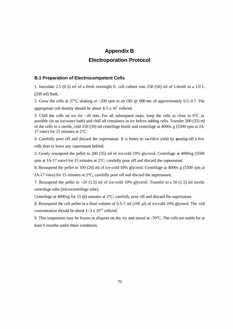
70
Appendix B
Electroporation Protocol
B.1 Preparation of Electrocompetent Cells
1. Inoculate 2.5 (0.5) ml of a fresh overnight E. coli culture into 250 (50) ml of L-broth in a 1.0 L
(250 ml) flask.
2. Grow the cells at 37°C shaking at ~200 rpm to an OD @ 600 nm of approximately 0.5–0.7. The
appropriate cell density should be about 4–5 x 10⁷ cells/ml.
3. Chill the cells on ice for ~20 min. For all subsequent steps, keep the cells as close to 0°C as possible (in an ice/water bath) and chill all containers in ice before adding cells. Transfer 200 (35) ml of the cells to a sterile, cold 250 (50) ml centrifuge bottle and centrifuge at 4000x g (5500 rpm at JA-17 rotor) for 15 minutes at 2°C.
4. Carefully pour off and discard the supernatant. It is better to sacrifice yield by pouring off a few
cells than to leave any supernatant behind.
5. Gently resuspend the pellet in 200 (35) ml of ice-cold 10% glycerol. Centrifuge at 4000xg (5500
rpm at JA-17 rotor) for 15 minutes at 2°C; carefully pour off and discard the supernatant.
6. Resuspend the pellet in 100 (20) ml of ice-cold 10% glycerol. Centrifuge at 4000x g (5500 rpm at
JA-17 rotor) for 15 minutes at 2°C; carefully pour off and discard the supernatant.
7. Resuspend the pellet in ~20 (1.5) ml of ice-cold 10% glycerol. Transfer to a 50 (1.5) ml sterile
centrifuge tube (microcentrifuge tube).
Centrifuge at 4000xg for 15 (6) minutes at 2°C; carefully pour off and discard the supernatant.
8. Resuspend the cell pellet in a final volume of 0.5–1 ml (100 µl) of ice-cold 10% glycerol. The cell
concentration should be about 1–3 x 10¹⁰ cells/ml.
9. This suspension may be frozen in aliquots on dry ice and stored at -70°C. The cells are stable for at
least 6 months under these conditions.

71
B.2 Electroporation
Gene Pulser Xcell conditions:
C = 25 µF; PC = 200 ohm; V = 2.5 kV, or
C = 25 µF; PC = 200 ohm; V = 3.0 kV (in 0.2 cm cuvettes).
1. Thaw the cells on ice. For each sample to be electroporated: place a 1.5 ml microfuge tube on ice,
place either a 0.2 cm electroporation cuvette on ice, and place 1 ml of SOC at room temperature.
2. To a cold, 1.5 ml polypropylene microfuge tube, add 20–40 µl of cell suspension. Add 1 to 5 µl of
DNA (DNA should be in a low ionic strength buffer such as water or TE). Mix well and incubate on
ice for ~1 minute. (Note: it is best to mix the plasmids and cells in a microfuge tube since the narrow
gap of the cuvettes prevents uniform mixing.)
3. From the Home screen on Gene Pulser Xcell open the Pre-set Protocols screen, then the Bacterial
Protocol screen (press 4, then Enter twice). When using the 0.2 cm cuvettes, press 2 then Enter, or 3
then Enter, to select the Protocol Detail screens for E. coli to pulse at 2.5 or 3.0 kV, respectively.
4. Transfer the mixture of cells and DNA to a cold electroporation cuvette and tap the suspension to
the bottom. Place the cuvette in the ShockPod. Push the chamber lid down to close.
5. Pulse once.
6. Remove the cuvette from the chamber and immediately add 1 (0.45) ml of SOC medium to the
cuvette.
Quickly but gently resuspend the cells with a Pasteur pipette. (The period between applying the pulse
and transferring the cells to outgrowth medium is crucial for recovering E. coli transformants (Dower
et al., 1988). Delaying this transfer by even 1 minute causes a 3-fold drop in transformation. This
decline continues to a 20-fold drop by 10 minutes.)
7. Transfer the cell suspension to a microcentrifuge tube and incubate at 37°C for 1 hour, shaking at
200 rpm.
8. Check and record the pulse parameters. The time constant should be close to 5 milliseconds. The
field strength can be calculated as actual volts (kV) / cuvette gap (cm).
9. Plate on LB plates with antibiotic.

72
B.3 Solutions and Reagents
1. L-Broth: 10 g Tryptone peptone, 5 g Yeast extracts, 5 g NaCl; dissolve in 1.0 L water.
Autoclave.
2. LB agar plates with selective antibiotic: prepare L broth as above, adding 15 g of agar per liter.
Autoclave. Cool to 55–60°C and add antibiotic. Pour 12–15 ml per 100 mm plate.
3. 10% (v/v) Glycerol: 12.6 g glycerol (density = 1.26 g/cc) in 90 ml of water. Autoclave or filter
sterilizing.
4. TE: 10 mM Tris-HCl pH 8.0, 1 mM EDTA.
5. SOB: 2.0 g Tryptone peptone, 0.5 g Yeast extract, 0.2 ml 5 M NaCl, 0.25 ml 1 M KCl; dissolve in
90 ml water. Adjust pH to 7.0. Bring volume to 100 ml. Autoclave. Add 1.0 ml sterile 1 M MgCl2
and 1.0 ml sterile 1 M MgSO4.
6. SOC: to 100 ml SOB, add 2.0 ml sterile 1 M glucose (sterilize by filtration).