Embed Size (px)
Citation preview
Design of a Low-Dropout Regulator with On-Chip Frequency Compensation
Jian XIAO, Yanzhang QIU, Yunxia GAO, Hongliang CHEN
Institute of Electronics and Control, Chang’an University, Xi’an, P.R. China, 710064 Email: [email protected]
Abstract: Designed a Low-Dropout (LDO) Regulator, analyzed the circuit structure and the sub-circuit de-sign With On-chip Frequency Compensation. Presented a novel internal frequency compensation circuit, ful-filled the use of low equivalent series resistance (ESR) load capacitor, and an accurate over-current protection circuit is realized, thus improves transient response and reduce the cost greatly. Test result proved the feasi-bility of this method, the measured typical dropout voltage is 100mV, operating voltage range is 2.5V-7V, output overshoot voltage is less than 50mV when load current stepped from 1mA to 500mA.
Keywords: CMOS; regulator; frequency compensation; stability 1 Introduction With the reduced power supply voltage and chip size, power consumption became an increasingly problem. As a result, LDO design has become more challenging [1-8]. Methods to improve the classic LDO structure have been proposed [1-5], However, the limitation of the classical LDOs is mainly due to the associated single pole-zero cancellation scheme, in which an off-chip capacitor with a high ESR is required to achieve low-frequency pole-zero cancellation. Use multilayer ceramic capacitor is an active solution for improving transient responses, but this method may cause oscillation. So generate the on-chip zero became the key technique to improve LDO performance. Many papers report some methods, but the circuits are complex and the zero has a large variety range.
This paper presents a new structure to achieve low dropout voltage regulators, through the frequency com-pensation for two stage push-pull output error amplifier, allowing adjustment of the parasitic poles to outside the unit gain frequency (UGF) that located in the gate of pass device. Push-pull output increased the transition rate, thus greatly improved the loop transient response; In addition, the LDO feedback loop adds a new frequency compensation circuit, the circuit structure is simple, the zero is independent with load variety, so ensured the sta-bility of LDO at the same time to achieve an external low ESR output capacitors.
2 LDO Circuit Structure The traditional LDO regulator using a single-stage am-plifier with good frequency response and bandwidth, the dominant pole is located in the output of LDO and non-dominant pole in the gate of pass device, using the output capacitor ESR zero to achieve pole-zero cancella-tion [1,2,3]. This method have restricted requirements, range of ESR is limited to 0.1 ~ 10Ω [3], in order to get a
better temperature characteristics, the tantalum capacitor usually selected, its disadvantages are both large size and higher prices. In addition, the overshoot of output voltage is proportional to ESR, this may cause the output voltage out of range in low-voltage working conditions, ever get a logic wrong in the high speed digital circuit.
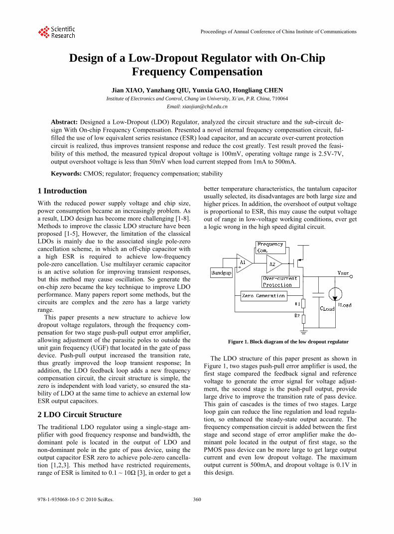
Figure 1. Block diagram of the low dropout regulator
The LDO structure of this paper present as shown in
Figure 1, two stages push-pull error amplifier is used, the first stage compared the feedback signal and reference voltage to generate the error signal for voltage adjust-ment, the second stage is the push-pull output, provide large drive to improve the transition rate of pass device. This gain of cascades is the times of two stages. Large loop gain can reduce the line regulation and load regula-tion, so enhanced the steady-state output accurate. The frequency compensation circuit is added between the first stage and second stage of error amplifier make the do-minant pole located in the output of first stage, so the PMOS pass device can be more large to get large output current and even low dropout voltage. The maximum output current is 500mA, and dropout voltage is 0.1V in this design.
360978-1-935068-10-5 © 2010 SciRes.
Proceedings of Annual Conference of China Institute of Communications

There are tree low frequency pole located in the first stage output of error amp(P1), the second stage out-put(P3), the output of LDO(P2), the zero(Z1) generated by the frequency compensation circuit of error amplifier and zero generated by the zero generation circuit are used to cancel the P3 and p2, so fulfilled the frequency com-pensation of the while circuit. The multilayer ceramic capacitor can be used for its advantage of low ESR; this makes the zero far away from UGF of LDO output. The reference is a bandgap reference, over-current protection circuit detect the current of LDO, while the current ex-ceed the limitation, the pass device can be turn off. Through careful design for the location of zero and pole position inside the UGF, we can get enough phase mar-gin to ensure the LDO stability for the entire loop in a variety of output load current.
3 CMOS Circuit Implementation
3.1 The Frequency Compensation Circuit
Figure 2. Schematic of the frequency compensation
The presented LDO exits two low frequency poles lo-
cated in the first stage output of the error amplifier and the output of LDO respectively. We introduced a zero generation circuit to achieve the stability of the LDO, as shown in Figure 2, Its output connected between the se-ries resistor R1 and R2, and feedback to the first stage input of error amplifier, the input then connected to the output of LDO. Consider the left part of the zero genera-tion circuit, its transfer function as follows:
21
2 22 2
2 2
11 /( )
11/ 1 /( )
gs gm
m dsm ds
g ds gs
sC Rg
H s g rg r sR r C
+⋅
= ⋅++ ++ ⋅
(1)
we can see that select suitable parameters can force the pole far away from the zero, and also can located the pole outside the UGF, thus without effect on the stability of the loop. Times of Rg and Cgs2 generate a fixed left-half plane
zero, this zero should locate in the 10 times of pole lo-cated in the first stage output of the error amplifier to cancel P1. We can precisely control the zero position, thus greatly improves the loop stability and noise suppression compared to the traditional structure.
3.2 Error Amplifier Design
Vref
Vfb
Vbn
A B
A
R1 C1
C2
VDD
M21
M22
M21
M11 M12
M13 M14
M15
M16
M17
M18
M19
M20
.
Figure 3. Schematic of the error amplifier
Design of the error amplifier needs to meet the re-
quirements of loop gain, transient response and stability. In our design, two stage error amplifier is used as shown in Fig.3, the first stage is a differential amplifier with current mirror load, the second stage use a push-pull structure, generating sufficient output voltage swing, as well as faster response speed which greatly improve LDO's transient response. The first stage output drives PMOS transistor M21 and NMOS transistor M22 respec-tively, the gate of M19 connected to the output of over-current protection circuit for turn off the push pull loop while the output current is too large. C1 and C2 are the miller compensation capacitors, C1 in series with resistor R1 makes the right-half plane zero moved to left-half plane generated by the miller compensation, C1 and R1 values should be met:
1 11/ (2 )C Rπ =1/ (2 )g oaC Rπ (2)
So we can cancel the parasitic pole located in the gate of pass device, as well as makes the dominant pole lo-cated in the first stage output of error amplifier. Hspice simulation shows that the low frequency gain and phase margin of error amplifier is larger than 80dB and 84° respectively, at the condition of 5V input voltage and 80pF load capacitor.
3.3 The Over-current Protection Circuit This design of low dropout voltage regulator maximum output current up to 500mA, so stable and reliable over-current protection circuit is also one of the keys design. Over-current protection circuit diagram as shown in Figure 4, the PMOS transistor M23 and resistor RS parallel with the pass device constitute of a current sam-pling circuit, and also proportion to the size of pass de-
361 978-1-935068-10-5 © 2010 SciRes.
Proceedings of Annual Conference of China Institute of Communications
vice, thus implement the current sampling accurately. Through adjusting the resistance of RS to turn off the M24, turn on the M27, the low level output from the drain of M24 switched off the second stage loop of the error amplifier, the high level output switched off the pass device, in order to achieve accurate over-current protection.
O v e r - c u r r e n tP r o t e c t
c u r r e n tS a m p l e
R s
M 2 3
M 2 4
M 2 5
M 2 7
M 2 8
M 2 9
M 3 0
M 3 1
V B N 1
V B N 2
V b n
V D D
Figure 4. Schematic of the over-current protection
4 Simulation and Test Results Vanguard 0.5um CMOS mixed-signal technology is used for layout, an external output capacitor CLoad is 1uF, ESR of CLoad is less than 50mΩ. The current source of load use an ideal current source with range of 0mA ~ 500mA, open-loop gain of the Hspice simulation results show that the phase margin is 45 when load current is 500mA. The UGF decreases as the load current decreases, so the phase margin increased the loop more stable. Fig.5 is the transient load regulation results while the current stepped from 10mA to 500mA, showing that the largest over-shoot voltage is 50mV, transition time is less than 1us. Fig.6 is a test chip micrograph.
5 Summary
Figure 5. Response of transient load regulation((X-axis 1us/div, Y-axis 50mV/div)
Figure 6. Die micrograph of the Regulator chip
We presented a new single-chip CMOS low dropout
voltage regulator approach, a internal frequency com-pensation circuit is used to implement the loop stability that can provides accurate load-independent frequency compensation, thus an external multi-layer ceramic ca-pacitors can be used, which greatly reduce costs and im-prove transient response. The static power dissipation and layout area are not increased Compared with con-ventional CMOS regulator, the LDO load regulation and line regulation are not affected for the additional fre-quency compensation circuit. Vanguard 0.5um CMOS process is used for verification, the test results show that the typical value of dropout voltage is 100mV as the output current is 500mA, and operation voltage range is 2.5V-7V.
References [1] Leung Ka Nang, Philip K T Mok, Wing Hung Ki. A Novel Fre-
quency Compensation Technique for Low-Voltage Low-Dropout Regulator [C].//IEEE International Symposium on Circuits and Systems, Florida: Orlando, 1999: 102–105.
[2] Rincon-Mora G A. Active capacitor multiplier in Miller-com-pensated circuits [J]. IEEE. J. Solid-State circuits, 2000, 35: 26–32.
[3] “ESR, Stability, and the LDO Regulator,” Texas Instruments, Dallas, TX, Texas Instruments Data Sheet, REG115, 2002.
[4] Chava C K, Silva-Martinez J. A Frequency Compensation Scheme for LDO Voltage Regulator[J]. IEEE Trans, Circuits Syst. I, 2004, 51: 1041–1050.
[5] Leung Ka Nang, Philip K T Mok. Analysis of multistage ampli-fier-frequency compensation[J]. IEEE Trans, Circuits Syst. I, 2002, 48: 1041–1056
[6] Ka Chun Kwok and Philip K. T. Mok, “Pole-Zero Tracking frequency Compensation for Low Dropout Regulator,” IEEE SCAS, 2002.
[7] Wei. Jen Huang, Sao.Hung Lu, Shen—luan Liu. A Capaci-tor-free CMOS Low Dropout Regulator with Slew Rate En-hancement International Symposium on VLSI Design, Automa-tion and Test[c], 2006, 4: 1–4.
[8] Robert J Milliken, Jose Silva.Martinez, Edgar Sanchez-Sinencio, Full On-Chip CMOS Low-Dropout Voltage Regulator[J]. IEEE Transactions on Circuits and Systems, 2007, 54(9): 1879–1890.
362978-1-935068-10-5 © 2010 SciRes.
Proceedings of Annual Conference of China Institute of Communications