Embed Size (px)
Citation preview
Power Supply Design Seminar
Design of a high-frequency series capacitor buck converter
Reproduced from 2016 Texas Instruments Power Supply Design Seminar SEM2200
TI Literature Number: SLUP337 © 2016, 2017 Texas Instruments Incorporated
Power Seminar topics and online power training modules are available at:ti.com/psds
Texas Instruments – 2016/17 Power Supply Design Seminar
Design of a high-frequency series capacitor buck converter
Pradeep Shenoy
Texas Instruments – 2016/17 Power Supply Design Seminar
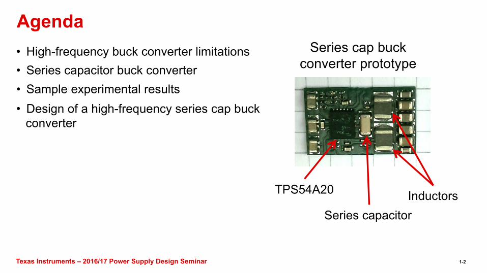
Agenda • High-frequency buck converter limitations• Series capacitor buck converter• Sample experimental results• Design of a high-frequency series cap buck
converter
Series cap buck converter prototype
TPS54A20
Series capacitor Inductors
1-2
Texas Instruments – 2016/17 Power Supply Design Seminar
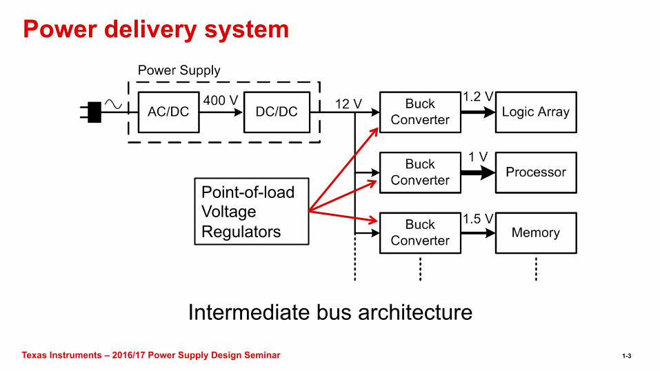
Power delivery system
Intermediate bus architecture
Point-of-load Voltage Regulators
1-3
Texas Instruments – 2016/17 Power Supply Design Seminar
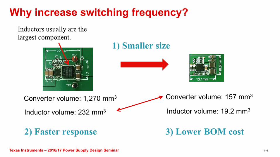
Why increase switching frequency? Inductors usually are the largest component.
1) Smaller size
2) Faster response 3) Lower BOM cost
Converter volume: 1,270 mm3 Converter volume: 157 mm3
Inductor volume: 232 mm3 Inductor volume: 19.2 mm3
1-4
Texas Instruments – 2016/17 Power Supply Design Seminar
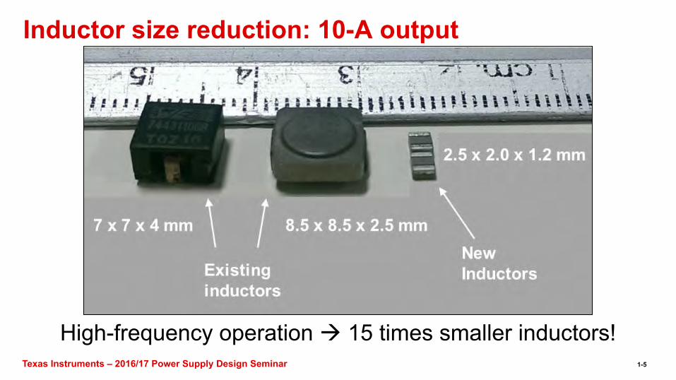
Inductor size reduction: 10-A output
High-frequency operation ! 15 times smaller inductors!
500 kHz
2-5 MHz
1-5
Texas Instruments – 2016/17 Power Supply Design Seminar
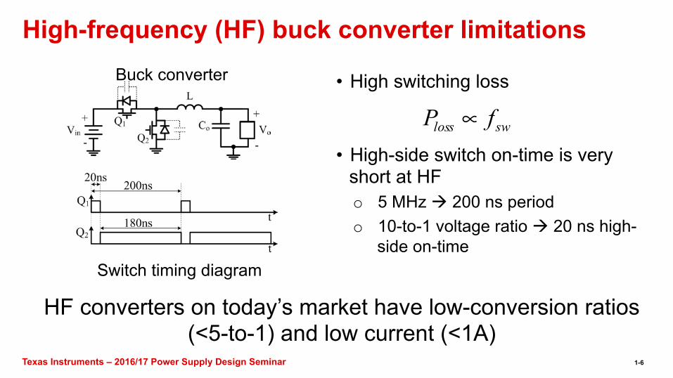
High-frequency (HF) buck converter limitations
• High switching loss
• High-side switch on-time is veryshort at HFo 5 MHz ! 200 ns periodo 10-to-1 voltage ratio ! 20 ns high-
side on-time
Buck converter
Switch timing diagram
HF converters on today’s market have low-conversion ratios (<5-to-1) and low current (<1A)
swloss fP ∝
1-6
Texas Instruments – 2016/17 Power Supply Design Seminar
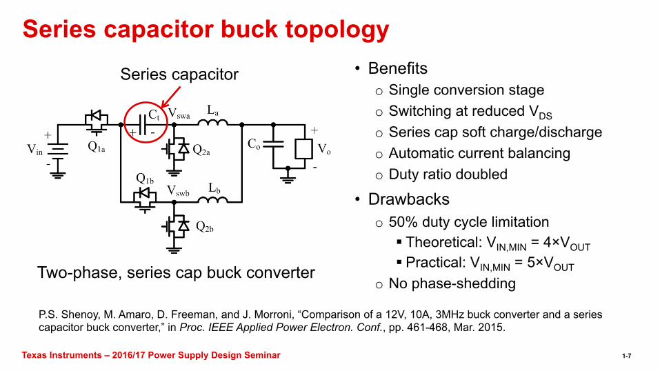
Series capacitor buck topology • Benefits
o Single conversion stage o Switching at reduced VDS o Series cap soft charge/discharge o Automatic current balancing o Duty ratio doubled
• Drawbacks o 50% duty cycle limitation
" Theoretical: VIN,MIN = 4×VOUT " Practical: VIN,MIN = 5×VOUT
o No phase-shedding Two-phase, series cap buck converter
Series capacitor
P.S. Shenoy, M. Amaro, D. Freeman, and J. Morroni, “Comparison of a 12V, 10A, 3MHz buck converter and a series capacitor buck converter,” in Proc. IEEE Applied Power Electron. Conf., pp. 461-468, Mar. 2015.
1-7
Texas Instruments – 2016/17 Power Supply Design Seminar
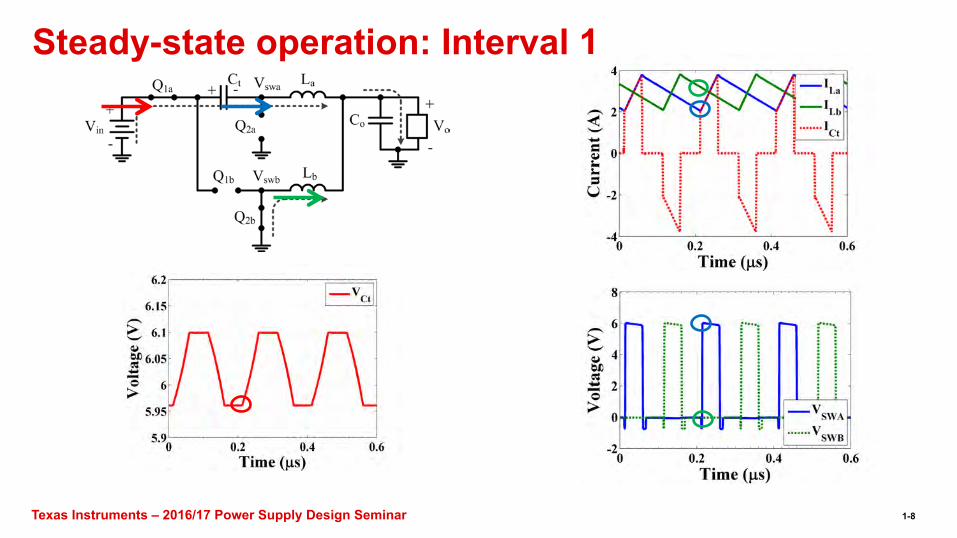
Steady-state operation: Interval 1
1-8
Texas Instruments – 2016/17 Power Supply Design Seminar
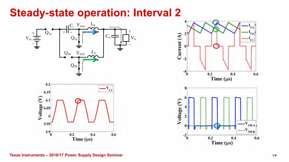
Steady-state operation: Interval 2
1-9
Texas Instruments – 2016/17 Power Supply Design Seminar
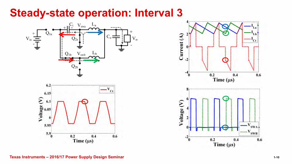
Steady-state operation: Interval 3
1-10
Texas Instruments – 2016/17 Power Supply Design Seminar
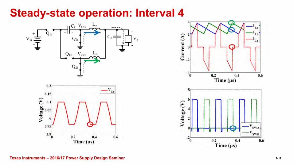
Steady-state operation: Interval 4
1-11
Texas Instruments – 2016/17 Power Supply Design Seminar
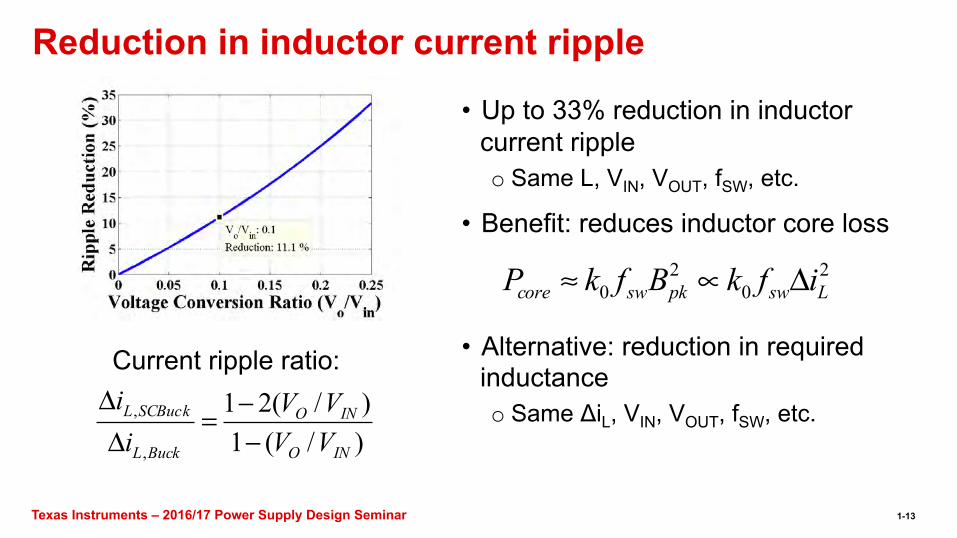
Reduction in inductor current ripple
• Up to 33% reduction in inductor current ripple o Same L, VIN, VOUT, fSW, etc.
• Benefit: reduces inductor core loss
• Alternative: reduction in required inductance o Same ΔiL, VIN, VOUT, fSW, etc.
Current ripple ratio:
20
20 Lswpkswcore ifkBfkP Δ∝≈
)/(1)/(21
,
,
INO
INO
BuckL
SCBuckL
VVVV
ii
−−=
ΔΔ
1-13
Texas Instruments – 2016/17 Power Supply Design Seminar
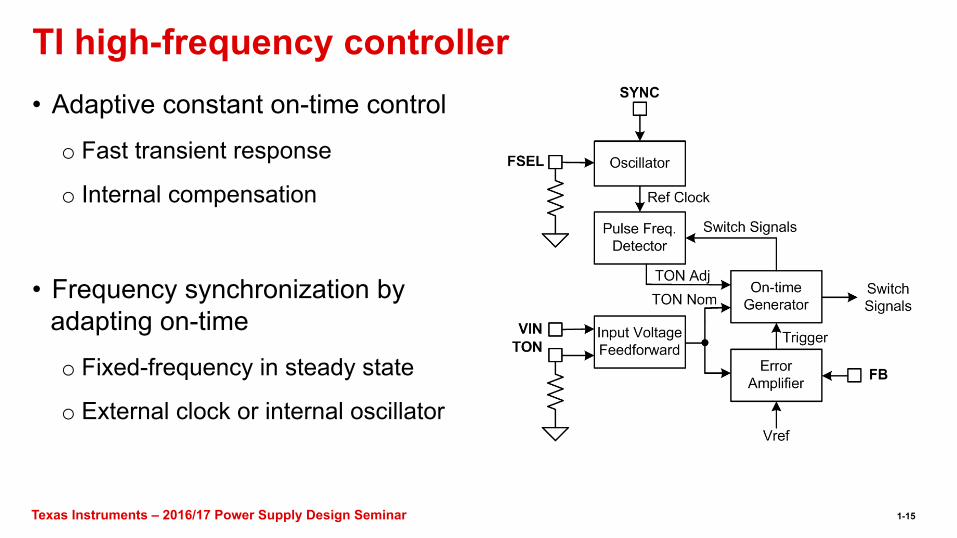
TI high-frequency controller • Adaptive constant on-time control
o Fast transient response
o Internal compensation
• Frequency synchronization byadapting on-time
o Fixed-frequency in steady state
o External clock or internal oscillator
1-15
Texas Instruments – 2016/17 Power Supply Design Seminar
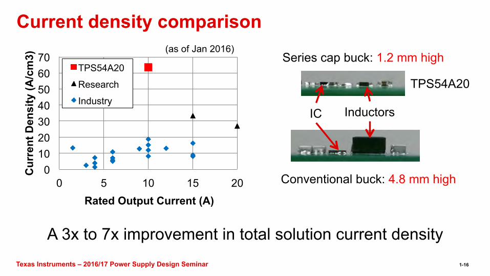
Current density comparison
A 3x to 7x improvement in total solution current density
Series cap buck: 1.2 mm high
Conventional buck: 4.8 mm high
IC Inductors
0 10 20 30 40 50 60 70
0 5 10 15 20
Cur
rent
Den
sity
(A/c
m3)
Rated Output Current (A)
TPS54A20
Research
Industry
TPS54A20
(as of Jan 2016)
1-16
Texas Instruments – 2016/17 Power Supply Design Seminar
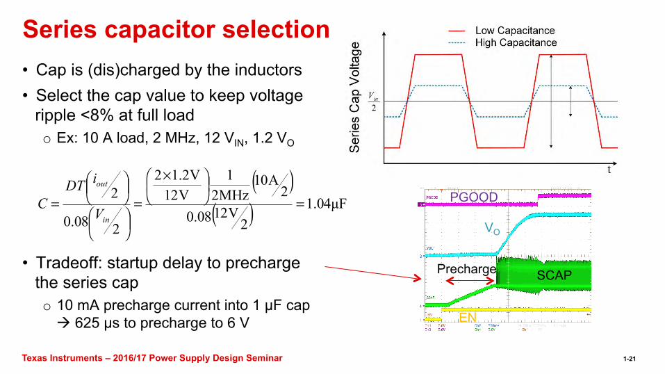
Series capacitor selection • Cap is (dis)charged by the inductors• Select the cap value to keep voltage
ripple <8% at full loado Ex: 10 A load, 2 MHz, 12 VIN, 1.2 VO
• Tradeoff: startup delay to prechargethe series capo 10 mA precharge current into 1 µF cap! 625 µs to precharge to 6 V
( )( ) µF04.1
2V1208.0
2A10
MHz21
V12V2.12
208.0
2=
⎟⎠⎞⎜
⎝⎛ ×
=⎟⎠⎞⎜⎝
⎛
⎟⎠⎞⎜⎝
⎛
=in
out
V
iDTC
Precharge
VO
PGOOD
SCAP
EN
1-21
Texas Instruments – 2016/17 Power Supply Design Seminar
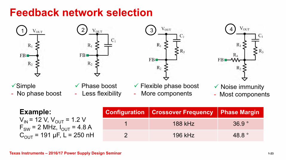
Feedback network selection
Configuration Crossover Frequency Phase Margin
1 188 kHz 36.9 °
2 196 kHz 48.8 °
# Simple - No phase boost
# Phase boost - Less flexibility
# Flexible phase boost - More components
# Noise immunity - Most components
Example: VIN = 12 V, VOUT = 1.2 V FSW = 2 MHz, IOUT = 4.8 A COUT = 191 µF, L = 250 nH
1 2 3 4
1-23
Texas Instruments – 2016/17 Power Supply Design Seminar
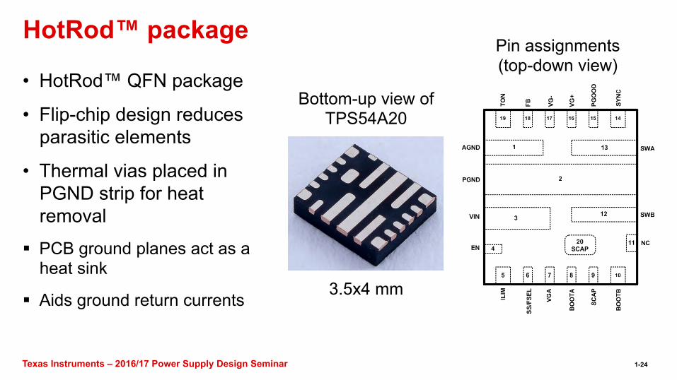
HotRod™ package
Bottom-up view of TPS54A20
Pin assignments (top-down view)
• HotRod™ QFN package
• Flip-chip design reducesparasitic elements
• Thermal vias placed inPGND strip for heatremoval
" PCB ground planes act as a heat sink
" Aids ground return currents 3.5x4 mm
1-24
Texas Instruments – 2016/17 Power Supply Design Seminar
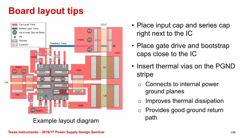
Board layout tips • Place input cap and series cap
right next to the IC
• Place gate drive and bootstrapcaps close to the IC
• Insert thermal vias on the PGNDstripeo Connects to internal power
ground planeso Improves thermal dissipationo Provides good ground return
pathExample layout diagram
1-25
Texas Instruments – 2016/17 Power Supply Design Seminar
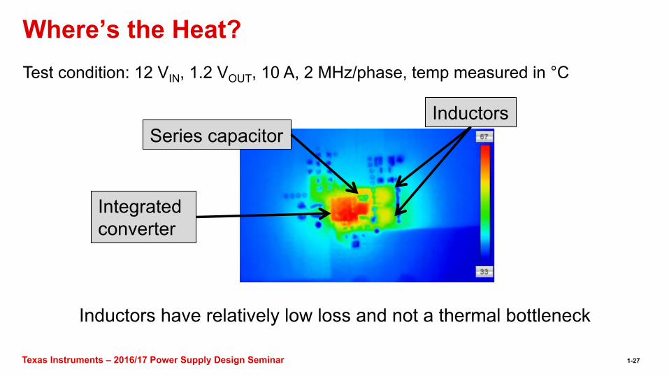
Where’s the Heat?
Integrated converter
Series capacitor Inductors
Test condition: 12 VIN, 1.2 VOUT, 10 A, 2 MHz/phase, temp measured in °C
Inductors have relatively low loss and not a thermal bottleneck
1-27
Texas Instruments – 2016/17 Power Supply Design Seminar
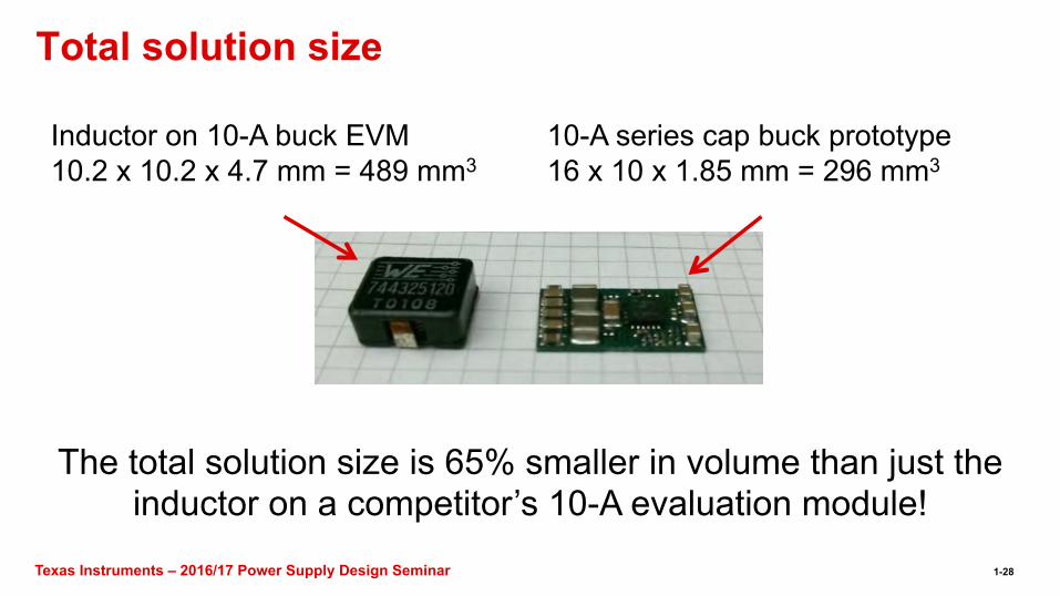
Total solution size
10-A series cap buck prototype 16 x 10 x 1.85 mm = 296 mm3
Inductor on 10-A buck EVM 10.2 x 10.2 x 4.7 mm = 489 mm3
The total solution size is 65% smaller in volume than just the inductor on a competitor’s 10-A evaluation module!
1-28
Texas Instruments – 2016/17 Power Supply Design Seminar
Summary
• High-frequency (HF) operation of switching convertersenables size reduction and performance improvements
• Buck converters have fundamental limitations that limit HFoperation
• The series capacitor buck converter has uniqueproperties that support HF operation
• Design guidelines for an HF series cap buck converterdemonstrate the ease of implementation
1-29
Texas Instruments – 2016/17 Power Supply Design Seminar
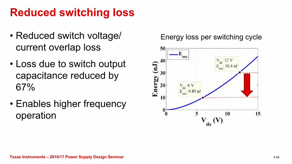
Reduced switching loss
• Reduced switch voltage/current overlap loss
• Loss due to switch outputcapacitance reduced by67%
• Enables higher frequencyoperation
Energy loss per switching cycle
1-12
Texas Instruments – 2016/17 Power Supply Design Seminar
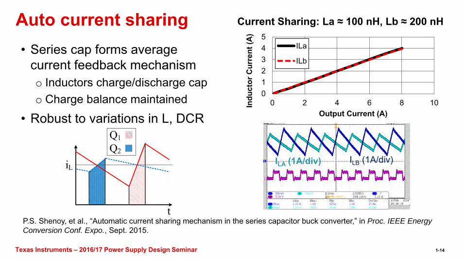
Auto current sharing
012345
0 2 4 6 8 10Indu
ctor
Cur
rent
(A)
Output Current (A)
ILa
ILb
ILA (1A/div) ILB (1A/div)
Current Sharing: La ≈ 100 nH, Lb ≈ 200 nH
• Series cap forms averagecurrent feedback mechanismo Inductors charge/discharge capo Charge balance maintained
• Robust to variations in L, DCR
P.S. Shenoy, et al., “Automatic current sharing mechanism in the series capacitor buck converter,” in Proc. IEEE Energy
Conversion Conf. Expo., Sept. 2015.
1-14
Texas Instruments – 2016/17 Power Supply Design Seminar
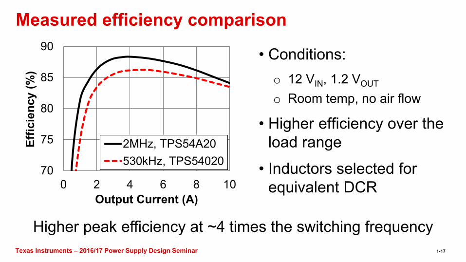
Measured efficiency comparison
• Conditions: o 12 VIN, 1.2 VOUT
o Room temp, no air flow
• Higher efficiency over the load range
• Inductors selected for equivalent DCR
Higher peak efficiency at ~4 times the switching frequency
70
75
80
85
90
0 2 4 6 8 10
Effic
ienc
y (%
)
Output Current (A)
2MHz, TPS54A20530kHz, TPS54020
1-17
Texas Instruments – 2016/17 Power Supply Design Seminar
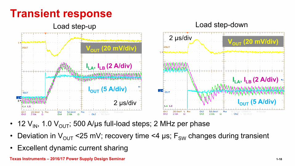
Transient response
• 12 VIN, 1.0 VOUT; 500 A/µs full-load steps; 2 MHz per phase• Deviation in VOUT <25 mV; recovery time <4 µs; FSW changes during transient• Excellent dynamic current sharing
IOUT (5 A/div)
ILA, ILB (2 A/div)
ILA, ILB (2 A/div)
VOUT (20 mV/div)
Load step-up Load step-down
VOUT (20 mV/div)
IOUT (5 A/div) 2 µs/div
2 µs/div
1-18
Texas Instruments – 2016/17 Power Supply Design Seminar
60
65
70
75
80
85
90
0 2 4 6 8 10
Effic
ienc
y (%
)
Output Current (A)
2MHz3.5MHz5MHz
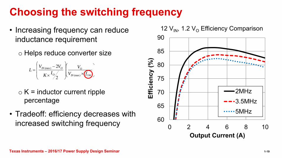
Choosing the switching frequency • Increasing frequency can reduce
inductance requirement
o Helps reduce converter size
o K = inductor current ripplepercentage
• Tradeoff: efficiency decreases withincreased switching frequency
SWIN
O
O
OIN
fV
V
IK
VVL
(max)
(max)
2
2
12 VIN, 1.2 VO Efficiency Comparison
1-19
Texas Instruments – 2016/17 Power Supply Design Seminar
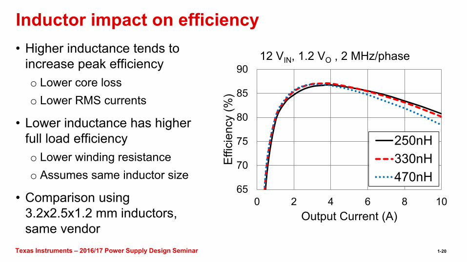
Inductor impact on efficiency • Higher inductance tends to
increase peak efficiency o Lower core loss o Lower RMS currents
• Lower inductance has higher full load efficiency o Lower winding resistance o Assumes same inductor size
• Comparison using 3.2x2.5x1.2 mm inductors, same vendor
65
70
75
80
85
90
0 2 4 6 8 10
Effi
cien
cy (%
) Output Current (A)
12 VIN, 1.2 VO , 2 MHz/phase
250nH330nH470nH
1-20
Texas Instruments – 2016/17 Power Supply Design Seminar
-40-20
0204060
1 10 100 1,000
Mag
nitu
de (d
B)
Frequency (kHz)
Co=91uFCo=138uF
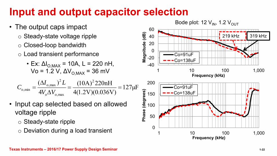
Input and output capacitor selection • The output caps impact
o Steady-state voltage rippleo Closed-loop bandwidtho Load transient performance
• Ex: ΔIO,MAX = 10A, L = 220 nH,Vo = 1.2 V, ΔVO,MAX = 36 mV
• Input cap selected based on allowedvoltage rippleo Steady-state rippleo Deviation during a load transient
219 kHz 319 kHz
Bode plot: 12 VIN, 1.2 VOUT
μF127)V036.0)(V2.1(4
nH220)A10(4
)( 2
max,
2max,
min,
oo
o
oVV
LIC
0
50
100
150
200
1 10 100 1,000
Phas
e (d
egre
es)
Frequency (kHz)
Co=91uFCo=138uF
1-22
Texas Instruments – 2016/17 Power Supply Design Seminar
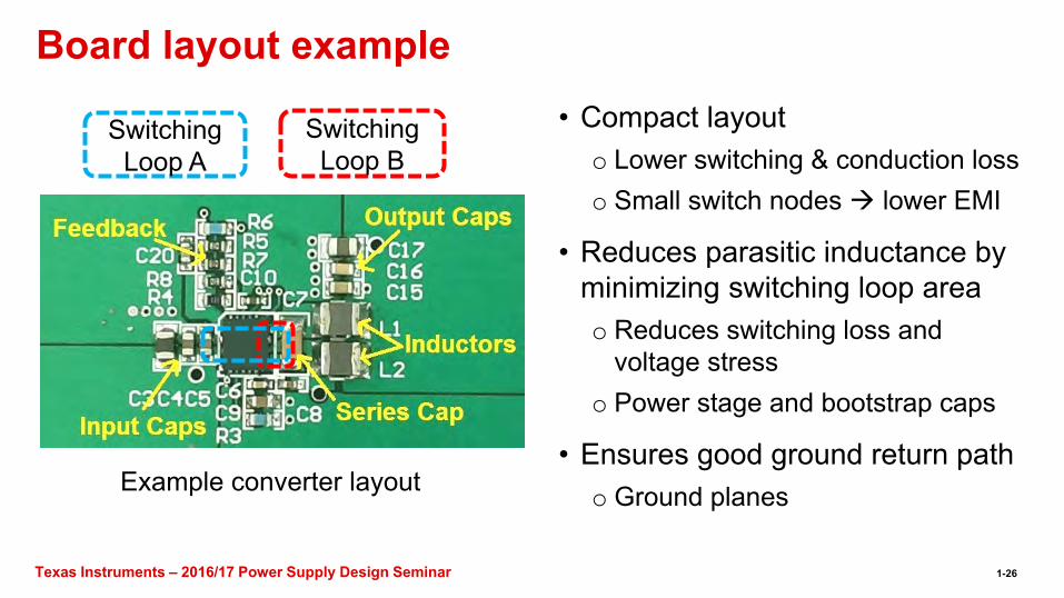
Board layout example • Compact layout
o Lower switching & conduction losso Small switch nodes lower EMI
• Reduces parasitic inductance byminimizing switching loop areao Reduces switching loss and
voltage stresso Power stage and bootstrap caps
• Ensures good ground return patho Ground planes
Switching Loop A
Switching Loop B
Example converter layout
1-26
The platform bar and E2E are trademarks of Texas Instruments. All other trademarks are the property of their respective owners. SLUP337
TI Worldwide Technical Support
InternetTI Semiconductor Product Information Center Home Pagesupport.ti.comTI E2E™ Community Home Pagee2e.ti.com
Product Information CentersPhone +1(512) 434-1560
Phone
Americas Brazil Mexico Phone
0800-891-2616
0800-670-7544
Fax Internet/Email
+1(972) 927-6377support.ti.com/sc/pic/americas.htm
Europe, Middle East, and AfricaPhone
European Free Call 00800-ASK-TEXAS (00800 275 83927)
International +49 (0) 8161 80 2121
Russian Support +7 (4) 95 98 10 701
Note: The European Free Call (Toll Free) number is not active in all countries. If you have technical difficulty calling the free call number, please use the international number above.
Fax Internet Direct Email
+(49) (0) 8161 80 2045www.ti.com/[email protected]
JapanPhone Domestic 0120-92-3326Fax International
Domestic +81-3-3344-5317
0120-81-0036Internet/Email International
Domestic support.ti.com/sc/pic/japan.htm
www.tij.co.jp/pic
AsiaPhone
+91-80-41381665International Domestic Toll-Free Number
Note: Toll-free numbers do not support mobile and IP phones.
1-800-999-084Australia China Hong Kong India Indonesia Korea Malaysia New Zealand Philippines Singapore
Taiwan Thailand
800-820-8682 800-96-5941000-800-100-8888 001-803-8861-1006 080-551-28041-800-80-3973 0800-446-9341-800-765-7404 800-886-1028 0800-006800001-800-886-0010
International Fax Email Internet
[email protected] or [email protected] support.ti.com/sc/pic/asia.htm
B021014
Important Notice: The products and services of Texas Instruments Incorporated and its subsidiaries described herein are sold subject to TI’s standard terms and conditions of sale. Customers are advised to obtain the most current and complete information about TI products and services before placing orders. TI assumes no liability for applications assistance, customer’s applications or product designs, software performance, or infringement of patents. The publication of information regarding any other company’s products or services does not constitute TI’s approval, warranty or endorsement thereof.
IMPORTANT NOTICE
Texas Instruments Incorporated and its subsidiaries (TI) reserve the right to make corrections, enhancements, improvements and otherchanges to its semiconductor products and services per JESD46, latest issue, and to discontinue any product or service per JESD48, latestissue. Buyers should obtain the latest relevant information before placing orders and should verify that such information is current andcomplete. All semiconductor products (also referred to herein as “components”) are sold subject to TI’s terms and conditions of salesupplied at the time of order acknowledgment.TI warrants performance of its components to the specifications applicable at the time of sale, in accordance with the warranty in TI’s termsand conditions of sale of semiconductor products. Testing and other quality control techniques are used to the extent TI deems necessaryto support this warranty. Except where mandated by applicable law, testing of all parameters of each component is not necessarilyperformed.TI assumes no liability for applications assistance or the design of Buyers’ products. Buyers are responsible for their products andapplications using TI components. To minimize the risks associated with Buyers’ products and applications, Buyers should provideadequate design and operating safeguards.TI does not warrant or represent that any license, either express or implied, is granted under any patent right, copyright, mask work right, orother intellectual property right relating to any combination, machine, or process in which TI components or services are used. Informationpublished by TI regarding third-party products or services does not constitute a license to use such products or services or a warranty orendorsement thereof. Use of such information may require a license from a third party under the patents or other intellectual property of thethird party, or a license from TI under the patents or other intellectual property of TI.Reproduction of significant portions of TI information in TI data books or data sheets is permissible only if reproduction is without alterationand is accompanied by all associated warranties, conditions, limitations, and notices. TI is not responsible or liable for such altereddocumentation. Information of third parties may be subject to additional restrictions.Resale of TI components or services with statements different from or beyond the parameters stated by TI for that component or servicevoids all express and any implied warranties for the associated TI component or service and is an unfair and deceptive business practice.TI is not responsible or liable for any such statements.Buyer acknowledges and agrees that it is solely responsible for compliance with all legal, regulatory and safety-related requirementsconcerning its products, and any use of TI components in its applications, notwithstanding any applications-related information or supportthat may be provided by TI. Buyer represents and agrees that it has all the necessary expertise to create and implement safeguards whichanticipate dangerous consequences of failures, monitor failures and their consequences, lessen the likelihood of failures that might causeharm and take appropriate remedial actions. Buyer will fully indemnify TI and its representatives against any damages arising out of the useof any TI components in safety-critical applications.In some cases, TI components may be promoted specifically to facilitate safety-related applications. With such components, TI’s goal is tohelp enable customers to design and create their own end-product solutions that meet applicable functional safety standards andrequirements. Nonetheless, such components are subject to these terms.No TI components are authorized for use in FDA Class III (or similar life-critical medical equipment) unless authorized officers of the partieshave executed a special agreement specifically governing such use.Only those TI components which TI has specifically designated as military grade or “enhanced plastic” are designed and intended for use inmilitary/aerospace applications or environments. Buyer acknowledges and agrees that any military or aerospace use of TI componentswhich have not been so designated is solely at the Buyer's risk, and that Buyer is solely responsible for compliance with all legal andregulatory requirements in connection with such use.TI has specifically designated certain components as meeting ISO/TS16949 requirements, mainly for automotive use. In any case of use ofnon-designated products, TI will not be responsible for any failure to meet ISO/TS16949.
Products ApplicationsAudio www.ti.com/audio Automotive and Transportation www.ti.com/automotiveAmplifiers amplifier.ti.com Communications and Telecom www.ti.com/communicationsData Converters dataconverter.ti.com Computers and Peripherals www.ti.com/computersDLP® Products www.dlp.com Consumer Electronics www.ti.com/consumer-appsDSP dsp.ti.com Energy and Lighting www.ti.com/energyClocks and Timers www.ti.com/clocks Industrial www.ti.com/industrialInterface interface.ti.com Medical www.ti.com/medicalLogic logic.ti.com Security www.ti.com/securityPower Mgmt power.ti.com Space, Avionics and Defense www.ti.com/space-avionics-defenseMicrocontrollers microcontroller.ti.com Video and Imaging www.ti.com/videoRFID www.ti-rfid.comOMAP Applications Processors www.ti.com/omap TI E2E Community e2e.ti.comWireless Connectivity www.ti.com/wirelessconnectivity
Mailing Address: Texas Instruments, Post Office Box 655303, Dallas, Texas 75265Copyright © 2016, Texas Instruments Incorporated