Embed Size (px)
Citation preview
Design of a Chopper Amplifier for
Use in Biomedical Signal Acquisition
by Abdelkader Hadj Said, Electronics Diploma
A Thesis Submitted in Partial Fulfillment of the Requirements for the Master of Science Degree
Department of Electrical and Computer Engineering in the Graduate School
Southern Illinois University Edwardsville Edwardsville, Illinois
December 2010
ii
ABSTRACT
DESIGN OF A CHOPPER AMPLIFIER FOR
USE IN BIOMEDICAL SIGNAL ACQUISITION
by
ABDELKADER HADJ SAID
Chairperson: Dr. George L Engel
In biomedical applications where a large dynamic range is required, the
design of a low-noise amplifier is critical. This thesis presents the design and
simulation of a low-noise pre-amplifier for use in biomedical signal acquisition.
Specifically, it is intended to be used in the front-end of an analog signal
processing channel that can be used in a multi-channel EcoG-based
(ElectrocorticoGraphic-based) BCI (Brain-Computer Interface) system currently
under development by Dr. Daniel Moran at Washington University in Saint Louis.
The design goal was to achieve a signal-to-noise ratio (SNR) of at least 6 dB
for a 90 Hz, 1µV peak-to-peak sinusoidal input signal. The target process, an ON-
Semiconductor 0.5 µm n-well process (C5N), like all CMOS processes possesses
poor flicker (1/f) noise characteristics. This is unfortunate given the low-frequency
nature (75 – 105 Hz) of our application. To minimize the 1/f noise introduced by
the amplifier, a chopper stabilization technique is utilized to overcome this
limitation.
The chopper pre-amplifier is implemented as a fully-differential circuit with
capacitive feedback. A pseudo-resistor which exploits the off-resistance of a
transistor is used to provide DC feedback stabilization. Moreover, we propose the
iii
use of a two-stage OTA (Operational Transconductance Amplifier) as the core
amplifier along with continuous-time common-mode feedback.
The chopper amplifier was analyzed theoretically with the help of MathCAD®
where the total noise contribution of the amplifier and the corresponding SNR were
computed. Estimates of the amplifier’s noise sources were based on the size and
the current bias of the input and load devices. The sizes of these devices and
biasing currents were limited to those consistent with our desire for a pre-amplifier
occupying a small area (much less than 1 mm2) and consuming little power (100
µWatts or less). The chopper amplifier was then simulated, at the behavioral level,
using MATLAB®. Finally, a full Veriloga-A model of the chopper amplifier (along
with the ECoG electrodes) was developed, and the circuit was simulated, at the
electrical level, using Cadence’s Spectre® simulator.
The chopper amplifier is estimated to occupy approximately 0.25 mm2,
dissipate 110 µW, and possess a 150 nV of integrated (input-referred) noise in the
75 – 105 Hz bandwidth of interest.

iv
ACKNOWLEDGEMENTS
I would like to express my sincere gratitude to my mentor Dr. George Engel
for his great guidance, support and encouragement. I am grateful for the
opportunity to work in the SIUE IC Design Research Laboratory. I have been
extremely honored to work under his supervision and learn from his advice and
useful insights throughout this project.
My special thanks to Dr. Brad Noble and Dr. Andy Lozowski who have
graciously agreed to serve on my master’s committee. Also, thanks goes out to Dr.
Scott Smith, Steve Muren, Dr. Oktay Alkin and all of the other ECE faculty
members for their support in completing my studies at SIUE.
I would also like to thank my fellow researchers, Vikram Vangapally and
Naveen Duggireddi, for the support they have offered me. Finally, I would like to
express my appreciation to my family and friends for their constant support.
v
TABLE OF CONTENTS
ABSTRACT ........................................................................................................... ii ACKNOWLEDGEMENTS ......................................................................................iv LIST OF FIGURES ...............................................................................................vii LIST OF TABLES ................................................................................................. ix Chapter 1. INTRODUCTION ........................................................................................ 1
Motivation.........................................................................................1 BCI Recording Technology .................................................................2 Goals and Thesis Organization ..........................................................6
2. SYSTEM LEVEL ANALYSIS ........................................................................ 8
Introduction ......................................................................................8 Chopper Stabilization Technique .....................................................10 The Chopper Amplifier.....................................................................12 Low-Noise OTA Topology .................................................................14 Noise Analysis .................................................................................19
3. SYSTEM LEVEL SIMULATION ................................................................. 28
Introduction............................................................................................. 28 MATLAB® Code Description ..................................................................... 28 MATLAB® Simulation Results ................................................................. 32
4. VERILOG-A BEHAVIORAL MODELING & IMPLEMENTATION ................... 34
Introduction............................................................................................. 34 The Chopper Amplifier.............................................................................. 34 Fully-differential op-amp ................................................................ 36 The amplifier ..........................................................................37 The modulators .....................................................................42 Modeling of Electrodes.....................................................................43 The Anti-Aliasing Filter (AAF)...........................................................45 The Signal Processing Block ............................................................46 The band-pass filter ...............................................................46 The notch filter.......................................................................47 Simulation of the Chopper Amplifier................................................48
vi
5. SUMMARY/FUTURE WORK ..................................................................... 53
Summary ................................................................................................. 53 Future Work ............................................................................................ 54
REFERENCES.................................................................................................... 56 APPENDICES ..................................................................................................... 58
A. MATCAD® Code .............................................................................. 58 B. MATLAB® Code............................................................................... 64 C. Verilog-A Code ................................................................................ 79
vii
LIST OF FIGURES
Figure Page
1.1 ECoG Array (64-Electrodes) Being Used With Subject ................................. 3
1.2 Block Diagram of Proposed Multichannel System........................................ 5
1.3 Architecture of Analog Signal Processing Module ........................................ 5
2.1 Chopper Stabilization Principle ([Tem:96]) ............................................... 10
2.2 Chopper Amplifier Architecture ............................................................... 12
2.3 Two-Stage OTA Design ............................................................................. 14
3.1 Signal Flow Diagram for a Matlab Simulation of the Chopper Amplifier ..... 30
3.2 Time-Domain Plot of the Chopper Amplifier .............................................. 32
3.3 Frequency-Domain Plot of the Amplifier With and Without Chopping ........ 33
4.1 Block Diagram for Simulation of the Chopper Amplifier at the Electrical Level ........................................................................................................ 35
4.2 Bode Plot of the Op-Amp .......................................................................... 36
4.3 Different Candidate Amplifiers: a) Fully-Differential Implementation, b) Single-Ended Using Real Resistors, c) Fully-Differential Using Diode-Connected pFETs, d) Single-Ended Using Diode-Connected pFETs............ 37
4.4 Magnitude Plot of Single-Ended Amplifier Using Real Resistors and Diode-Connected Transistors.............................................................................. 38
4.5 Transient Response of Amplifier for a 10mV Disturbance: (a) Using Real Resistors, (b) Using Diode-Connected FETs. ............................... 39
4.6 Transient Response of Amplifier for a 500mV Disturbance: (a) Using Real Resistors, (b) Using Diode-Connected FETs. ............................... 40
4.7 Bode Plot of Fully-Differential Amplifier Output Using Diode-Connected Transistors............................................................................................... 41
4.8 Time-Domain Simulation of Fully-Differential Amplifier Using 1mV Amplitude 90Hz Sine-Wave Input Signal................................................... 41
4.9 Schematic of Modulator Used in the Chopper Amplifier............................. 42
viii
4.10 Circuit Implementation of Switches .......................................................... 43
4.11 Block Diagram of the Electrodes ............................................................... 43
4.12 Magnitude Plots of Channel 4 and Channel 21 ......................................... 44
4.13 Bode Plot of Anti-Aliasing Filter ................................................................ 45
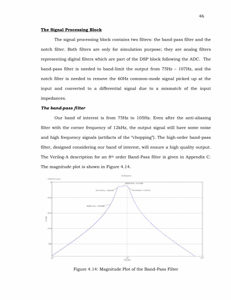
4.14 Magnitude Plot of the Band-Pass Filter ..................................................... 46
4.15 Magnitude Plot of the Notch Filter ............................................................ 47
4.16 Time-Domain Simulation of the Chopper Amplifier Using Identical Probes Without Adding Any Noise: (a) 90 Hz Input Signal, (b) Output of the Chopper, (c) Output of the Anti-Aliasing Filter, (d) Output of the Band-Pass Filter........................................................................................................ 48
4.17 Time-Domain Simulation of the Chopper Amplifier Using Different Probes Without Adding Any Noise: (a) 90 Hz Input Signal, (b) Output of Anti-Aliasing Filter, (c) Output of Band-Pass Filter, (d) Output of Notch Filter ... 49
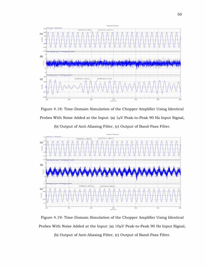
4.18 Time-Domain Simulation of the Chopper Amplifier Using Identical Probes With Noise Added at the Input: (a) 1µV Peak-to-Peak 90 Hz Input Signal, (b) Output of Anti-Aliasing Filter, (c) Output of Band-Pass Filter ............... 50
4.19 Time-Domain Simulation of the Chopper Amplifier Using Identical Probes With Noise Added at the Input: (a) 10µV Peak-to-Peak 90 Hz Input Signal, (b) Output of Anti-Aliasing Filter, (c) Output of Band-Pass Filter ............... 50
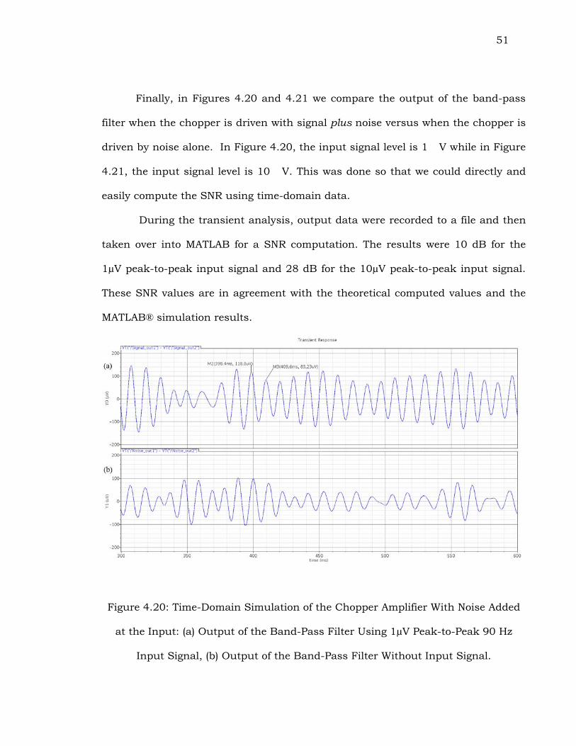
4.20 Time-Domain Simulation of the Chopper Amplifier With Noise Added at the Input: (a) Output of the Band-Pass Filter Using 1µV Peak-to-Peak 90 Hz Input Signal, (b) Output of the Band-Pass Filter Without Input Signal..... 51
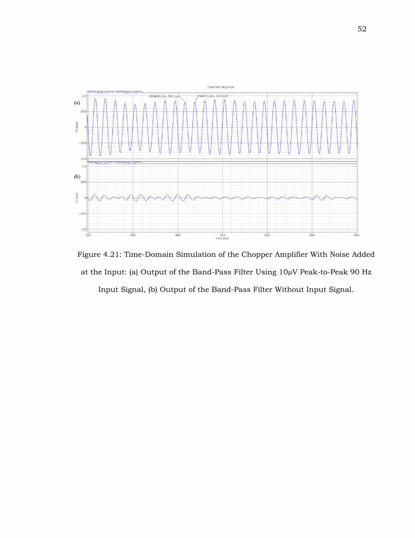
4.21 Time-Domain Simulation of the Chopper Amplifier With Noise Added at the Input: (a) Output of the Band-Pass Filter Using 10µV Peak-to-Peak 90 Hz Input Signal, (b) Output of the Band-Pass Filter Without Input Signal....... 52
ix
LIST OF TABLES
Table Page
2.1 ON-Semiconductor 0.5 Micron, N-well Process (C5N) Parameters ....... 9
2.2 Transistor Sizes for OTA........................................................................... 26
2.3 Summary of the Noise Analysis Parameters .............................................. 27
5.1 Summary of Noise Performance of the Chopper Amplifier.......................... 54
CHAPTER 1
INTRODUCTION
Motivation
The rapid growth in biotechnology has given birth to a new field:
neural engineering. This new field aims at linking human brain activity and man-
made devices in an effort to replace lost sensory and motor function [Sch:06]. A
Brain–Computer Interface (BCI) is a device which enables communication between
a brain and an external device. Since the beginning of research on BCIs in the
1970s at the University of California Los Angeles (UCLA), the BCI field has grown
enormously. The field has become focused on neuro-prosthetics applications that
aim at restoring damaged hearing, sight, and movement. Typically, neural
prosthetics connect the nervous system to a device, while BCIs usually connect the
brain with a computer system.
Brain-Controlled Interfaces convert brain signals into outputs that
communicate a user’s intent. BCIs can allow patients who are totally paralyzed to
express their wishes to the outside world [Leu:04]. A BCI makes use of recordings
of electrical activity associated with the scalp, the surface of the brain, or even from
within the cerebral cortex. These signals are then translated into command signals
that can drive prosthetic limbs, computer displays, etc.
Dr. Daniel Moran, Assistant Professor of Biomedical Engineering in the
School of Engineering and Applied Science at Washington University in Saint Louis
(WUSTL) is working in collaboration with Dr. Robert E. Morley, Associate
Professor of Electrical and Systems Engineering in the WUSTL School of
Engineering and Applied Science and Dr. George L. Engel, Professor of Electrical
2
and Computer Engineering in the Southern Illinois University Edwardsville (SIUE)
School of Engineering to advance BCI recording technology.
The collaboration looks to develop a custom, low-power, battery-operated
multi-channel ECoG (ElectroCorticoGraphic) BCI (Brain-Computer Interface)
telemetry system. The goal is to consolidate multiple analog circuits along with the
required Digital Signal Processing (DSP) functions into a custom ASIC (Application
Specific Integrated Circuit) and then pair the multi-channel ASIC with a
commercially available RF (Radio Frequency) telemetry chip.
BCI Recording Technology
Four primary techniques can be used for recording neural activity: the
electroencephalogram (EEG), the electrocorticographic activity (ECoG), local field
potentials (LFP) or single-unit action potentials. These recording modalities range
in resolution from single-unit recording (invasive method) to the measurement of
gross cortical activity using an electroencephalogram (EEG) non-invasive method.
Both local field potentials and single-unit action potentials are recorded from
within the brain parenchyma providing the highest quality signal (higher spatial
resolution!) but lack the necessary stability if long-term recordings are needed.
EEG recordings are considered safe and inexpensive but they have a relatively low
spatio-temporal resolution.
BCIs can use invasive or non-invasive methods. In practice, the choice of a
particular measurement approach is a balance of several system constraints,
including the measurement electrode’s spatial resolution, the desired neuro-
physiological information content, and the power requirements for sensing,
algorithm/control, and telemetry [Den:07].
3
An intermediate BCI methodology using electrocorticographic activity (ECoG)
recorded from the cortical surface can be a powerful and practical alternative to
these extremes. ECoG electrodes lie just above the cortex and average neural
activity over a smaller 0.5 cm range. ECoG has higher spatial resolution than EEG
(a typical EEG electrode located 2 cm above the cortex averages neural activity
across a 3 cm spatial extent [Sch:06]), broader bandwidth, higher amplitude, and
far less vulnerability to artifacts such as electro-myographic signals. At the same
time, because ECoG waveforms are recorded by subdural electrode arrays and thus
does not require electrodes that penetrate into the cortex, they are likely to have
greater long-term stability and might also be safer than single-neuron recording
[Leu:04].
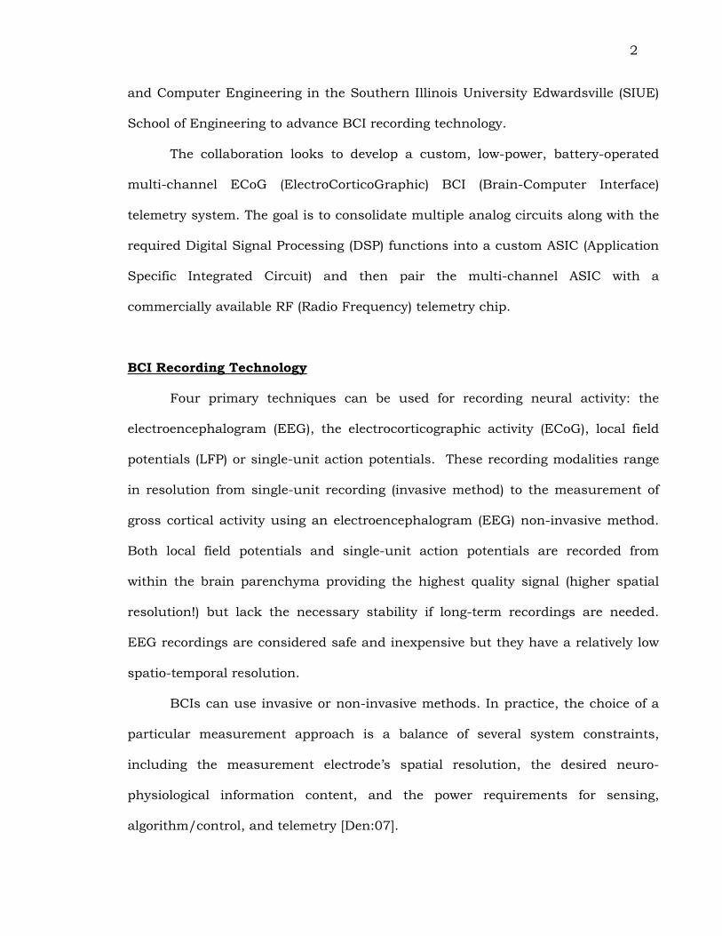
Research conducted by Dr. Moran primarily makes use of ECoG-based
systems. A 64-electrodes array shown in Figure.1.1a is attached to the surface of
the brain in Figure-1.1 (c).
Figure 1.1: ECoG Array (64-Electrodes) Being Used With Subject
4
In short, the ECoG modality provides a nice compromise between safety and
performance. While the use of LPFs and Single Units may offer superior
performance because of their higher spatial and temporal resolution, the use of
these modalities is certainly less common and is generally considered far less safe
for the subject [Sch:06]. It is for these reasons that proposed ASIC to be described
in the following section is targeted at BCIs that employ ECoG recordings.
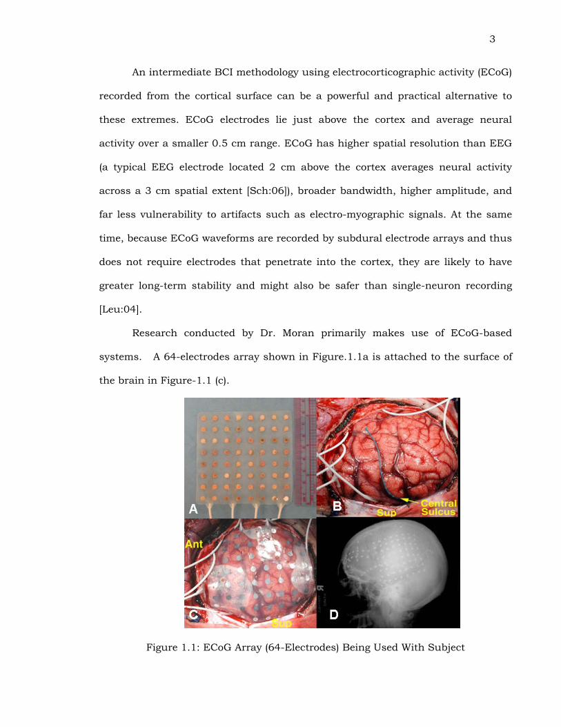
The proposed ASIC, depicted in Figure 1.2, will support the following features:
• Telemetry to PC (Personal Computer) for 8 ECoG channels in either raw or
compressed formats
• Each of the 8 channels chosen from one of eight groups of 4 electrodes with
reference chosen from one of four electrodes
• Bidirectional RF link for system configuration, control, and data telemetry
• Low-noise (fully-differential) electronics offering excellent SNR (Signal-to-
Noise Ratio) and CMRR (Common Mode Rejection Ratio)
• Adjustable signal bandwidths in each channel
• Low-power thereby allowing for rechargeable battery operation
• Variable RF data rates (and power consumption) of up to 500Kbps
• One week of typical use between recharging
5
Figure 1.2: Block Diagram of Proposed Multichannel System
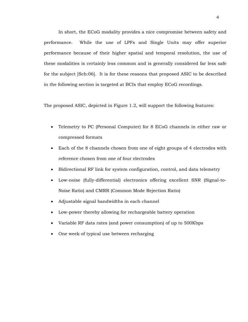
The architecture of the Analog Signal Processing (ASP) block is presented in
Figure 1.3. The differential signal associated with a selected pair of electrodes is
first amplified by a chopper-stabilized (CHS) pre-amplifier that provides gain
without introducing significant noise.
Figure 1.3: Architecture of Analog Signal Processing Module
6
The CHS amplifier is followed by a second-order, continuous-time low-pass
filter which provides additional gain and is used for anti-aliasing (AAF). The output
of the low-pass filter is then applied to a 16-bit ADC (a second-order Σ−Δ
converter). The output of the analog Σ−Δ modulator is a 1-bit 512 Ksample/sec
data stream. This high-speed 1-bit data is then processed by a digital signal
processing block to yield a 16-bit, 2000 samples/sec output stream.
Goals and Thesis Organization
In low-noise applications, the 1/f noise performance of the pre-amplifier is
often very important. There are two approaches to minimizing the 1/f noise of
CMOS op-amps (operational amplifiers). The first is to minimize the noise
contribution of the FETs (Field Effect Transistors) through circuit topology,
transistor selection (p-type versus n-type), and sizing (absolute area) of the FETs.
The second approach is to use an external means such as chopper stabilization to
remove 1/f noise associated with the input devices of the pre-amplifier that might
deteriorate the signal-to-noise ratio.
The main objective of this thesis is the design and simulation of a low-
power, low-noise chopper amplifier for use in multi-channel portable systems
which can be used for biomedical signal acquisition such as in the recording of
EcoG waveforms required by the proposed BCI. The aim is to minimize the 1/f
noise of the pre-amplifier predominantly through use of appropriate circuit
topology.
The thesis is divided into five chapters. Background information and a
general overview of the proposed BCI system, along with a description of the scope
of this thesis, is presented here in Chapter 1. Chapter 2 focuses on system-level
7
issues. The chapter begins with a description of the chopper-stabilization
technique, followed by an explanation of the topologies chosen for both the chopper
amplifier and its core amplifier. The chapter concludes with a detailed noise
analysis in the form of a MathCAD® design sheet. Chapter 3 discusses a
behavioral simulation of the proposed chopper amplifier using MATLAB®. Chapter
4 goes on to describe the implementation of the chopper amplifier using Verilog-A
behavioral modeling along with simulations performed using Cadence’s electrical
circuit simulator (Specte®). Results demonstrating the expected performance of the
proposed chopper pre-amplifier are presented. Finally, a summary of the
performance of the chopper amplifier and a discussion of future work which must
be successfully completed before the amplifier can be fabricated are presented in
Chapter 5.
8
CHAPTER 2
SYSTEM LEVEL ANALYSIS
Introduction
The chopper amplifier described in this thesis is intended to be used in the
front-end of a single analog signal processing channel that can be used in a multi-
channel EcoG-based BCI system. The purpose of amplifier is to amplify weak
bioelectrical signals from passive electrodes without introducing significant noise.
A CMOS (Complementary Metal Oxide Semiconductor) process is the target
fabrication technology. Specifically, we have selected the ON-Semiconductor 0.5
m n-well process known as C5N which is available through MOSIS (see
www.mosis.com) to fabricate the BCI ASIC.
The process was selected because it is a process that the SIUE IC Design
Research Laboratory has used for many years. It was also selected because it
allows dense digital circuits to be integrated on the same die as the analog
circuitry. This is important since a substantial digital signal processing block must
be integrated onto the multi-channel ASIC in the future. It is also less expensive to
fabricate CMOS circuits, and high resolution analog-to-digital conversion is best
achieved using CMOS technology
Relative to bipolar devices, MOS devices exhibit very high 1/f (i.e. flicker)
noise characteristics [Raz:01, All:03]. The 1/f noise issues are most acute in the
design of the chopper amplifier. In addition to the choice of an appropriate core
amplifier topology and judicious choice of transistor type and sizing, a chopper
stabilization technique is used to minimize 1/f (flicker) noise which is the result of
surface effects associated with the silicon – silicon dioxide interface associated with
9
all CMOS processes. Flicker noise is highly dependent upon wafer processing
details. The term 1/f arises from the fact that the power spectral density of flicker
noise displays a 1/f spectral characteristic and is therefore most troublesome in
low-frequency applications like the proposed BCI.
In the following sections, the chopper stabilization technique is first
presented, followed by a description of the topology chosen for the implementation
of the chopper amplifier. A core amplifier topology is then selected for use in the
chopper amplifier so that a detailed noise analysis can be performed. The
transistors in the core amplifiers that determine the noise, power, and area of the
core amplifier were sized. This was done to obtain good estimates of the total
noise, the total area occupied, and the total power consumption of the proposed
chopper amplifier.
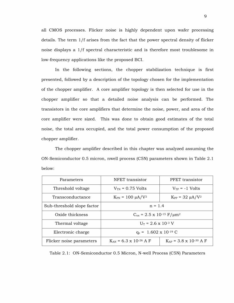
The chopper amplifier described in this chapter was analyzed assuming the
ON-Semiconductor 0.5 micron, nwell process (C5N) parameters shown in Table 2.1
below:
Parameters NFET transistor PFET transistor
Threshold voltage VTN = 0.75 Volts VTP = -1 Volts
Transconductance KPN = 100 µA/V2 KPP = 32 µA/V2
Sub-threshold slope factor n = 1.4
Oxide thickness Cox = 2.5 x 10⁻¹⁵ F/µm2
Thermal voltage UT = 2.6 x 10⁻³ V
Electronic charge qe = 1.602 x 10⁻¹⁹ C
Flicker noise parameters KAN = 6.3 x 10⁻²⁶ A F KAP = 3.8 x 10⁻³⁰ A F
Table 2.1: ON-Semiconductor 0.5 Micron, N-well Process (C5N) Parameters
10
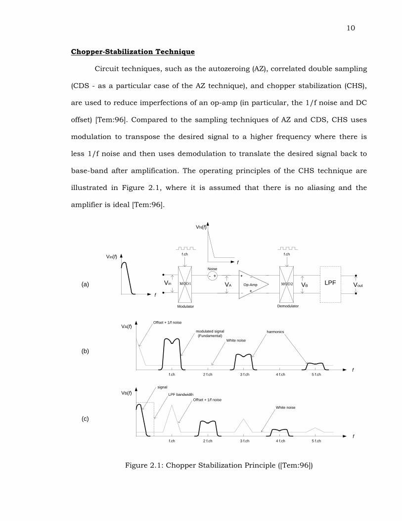
Chopper-Stabilization Technique
Circuit techniques, such as the autozeroing (AZ), correlated double sampling
(CDS - as a particular case of the AZ technique), and chopper stabilization (CHS),
are used to reduce imperfections of an op-amp (in particular, the 1/f noise and DC
offset) [Tem:96]. Compared to the sampling techniques of AZ and CDS, CHS uses
modulation to transpose the desired signal to a higher frequency where there is
less 1/f noise and then uses demodulation to translate the desired signal back to
base-band after amplification. The operating principles of the CHS technique are
illustrated in Figure 2.1, where it is assumed that there is no aliasing and the
amplifier is ideal [Tem:96].
VA(f)
f.ch 2 f.ch 3 f.ch 4 f.ch 5 f.chf
Offset + 1/f noise
modulated signal(Fundamental)
White noise
harmonics
VB(f)
f.ch 2 f.ch 3 f.ch 4 f.ch 5 f.chf
Offset + 1/f noise
signal
LPF bandwidth
White noise
Vin LPFVA VoutVB
Vin(f)
f
- +Noise
_
+
+
_
Op-Amp
VN(f)
f
Modulator
MOD1
f.ch
MOD2
f.ch
Demodulator
(a)
(b)
(c)
Figure 2.1: Chopper Stabilization Principle ([Tem:96])
11
First, the input signal is modulated to a higher frequency using a square-
wave carrier at the chopping frequency. Considering the Fourier series of a square-
wave given below, the input signal is converted to the odd harmonics frequencies of
the modulation signal.
( ) ( )( )( ) ( ) ( ) ( )∑
∞
=⎟⎠⎞
⎜⎝⎛ +++=
−⋅−
=1
...10sin516sin
312sin4
12212sin4
ksquare ftftft
kftktX πππ
ππ
π
After modulation, noise is added to the modulated signal to be amplified
together as shown in Figure 2.1b. Then the amplified signal is modulated using the
same square-wave used before. Therefore, the modulated input signal is
demodulated back to base-band while the noise is modulated to the odd harmonics
of the chopping frequency as shown in Figure 2.1c.
Finally, a low-pass filter is used to clean-up the output signal, removing the
modulated noise and artifacts. It is noted in [Tem:96] that:
• The finite bandwidth of the amplifier introduces some spectral components
around the even harmonics of the chopping frequency which have to be low-
pass filtered to recover the amplified signal
• In order to maintain a maximum DC gain, the phase shift between the input
and the output modulators has to match precisely the phase shift
introduced by the amplifier.
• Since the noise and the offset are modulated only once, they are transposed
to the odd harmonics of the output chopping square-wave, leaving the
amplifier ideally without any offset and low-frequency noise.
12
• The chopper modulators are most often realized using MOS switches with
non-idealities including clock feedback and charge injection. These non-
ideal effects associated with the switches give rise to residual offset.
• The residual offset can be reduced drastically, without losing too much
signal gain, by limiting the amplifier bandwidth to twice the chopper
frequency.
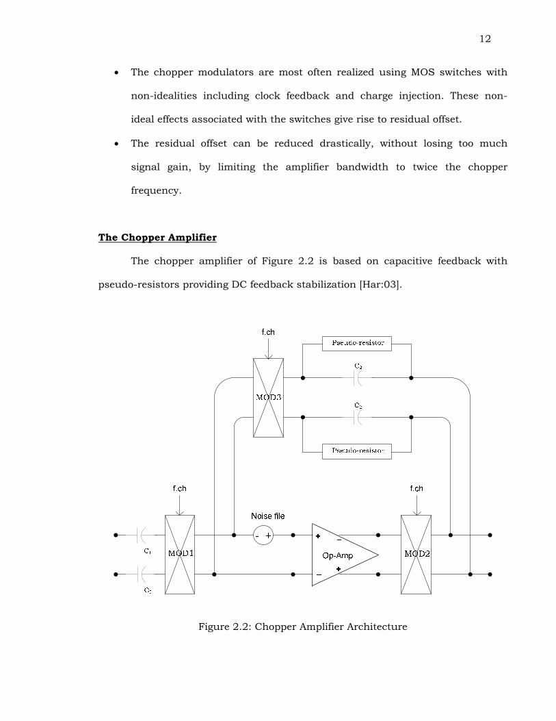
The Chopper Amplifier
The chopper amplifier of Figure 2.2 is based on capacitive feedback with
pseudo-resistors providing DC feedback stabilization [Har:03].
Figure 2.2: Chopper Amplifier Architecture
13
The gain of the amplifier is set by the ratio of the capacitors C1 and C2 (i.e.
C1/C2). Each of the pseudo-resistors in Figure 2.2 are realized using a pair of pFET
transistors that function either as a diode-connected pMOS transistor for a
negative gate-to-source voltage (Vgs < 0) or act as a diode-connected BJT for a
positive gate-to-source voltage (Vgs > 0). Two pFETs in series are used to reduce
distortion for large output signals [Har:03]. For small voltages across these devices,
their dynamic resistance is very high. Despite the long time-constant, given the
lower frequency corner of 1 Hz, a large change in the input causes a large voltage
across the MOS-bipolar elements thereby reducing their incremental resistance
which, in turn, results in a surprisingly fast settling time [Del:94].
The input signal is modulated by MOD1 to the odd harmonics of the
chopper frequency (16kHz). The chopping frequency was chosen as 16 kHz
because it was high enough so that the 1/f noise of the amplifier at 16 kHz could
be made sufficiently small without the need for extremely large transistors in the
core amplifier and because the resulting amplifier bandwidth of 32 kHz could be
achieved with small bias currents thereby reducing the power consumption of the
amplifier.
With the addition of the low frequency noise (1/f noise) and the inherent DC
offset of the amplifier, the signal is amplified and then the amplified signal is
demodulated back to baseband by the demodulator, MOD2, while the noise is
modulated to the chopper frequency i.e. 16 kHz. Modulator, MOD3, is used to
modulate the signal that is fed back to the summing node of the amplifier.
14
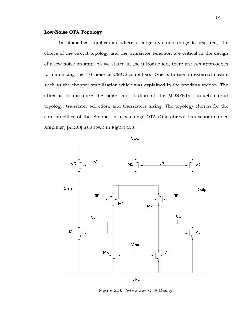
Low-Noise OTA Topology
In biomedical application where a large dynamic range is required, the
choice of the circuit topology and the transistor selection are critical in the design
of a low-noise op-amp. As we stated in the introduction, there are two approaches
to minimizing the 1/f noise of CMOS amplifiers. One is to use an external means
such as the chopper stabilization which was explained in the previous section. The
other is to minimize the noise contribution of the MOSFETs through circuit
topology, transistor selection, and transistors sizing. The topology chosen for the
core amplifier of the chopper is a two-stage OTA (Operational Transconductance
Amplifier) [All:03] as shown in Figure 2.3.
Figure 2.3: Two-Stage OTA Design
15
A two-stage design is warranted because it must be able to drive the resistive load
presented by the anti-aliasing filter which will follow it.
The advantages of a fully-differential version, compared to its single-ended
counterpart, is that it is less susceptible to common-mode noise and provides a
larger output swing which is important when the power supply is small (our supply
here 3.6 V while the process is really intended for 5 V operation). Yet the op-amp
requires two matched feedback networks and a common-mode feedback circuit,
used to control the common-mode output voltage [Gra:01].
To minimize the 1/f noise, the input devices of two-stage OTA are chosen to
be PFETs because they present about 100 times less 1/f noise compared to the
NFETs in the target 0.5 µm C5N process (see KAN and KAP values in Table 2.1). Also,
it is important to make the gain of the first stage as high as possible, and to make
the lengths of the load devices (FETs M3 and M4) greater than the lengths of the
input devices (FETs M1 and M2) to reduce the overall noise.
In addition, in order to maintain stability, compensation capacitors should
be connected across the second stages. The compensation capacitors in Figure 2.3
were also used to control the Gain-Bandwidth (GBW) product of the core amplifier
and in turn the bandwidth of the amplifier. Recall, it is important that the
bandwidth of the amplifier be made about twice the chopping frequency or about
32 kHz.
The total equivalent input-referred noise power of the two-stage OTA [All:3,
Raz:01] of Figure 2.3 is given by
( )2
1
27
26
2
21
23
2
1
321
2 212
v
nn
n
n
m
mneq A
VVVV
gg
VV+⋅
+⎥⎥
⎦
⎤
⎢⎢
⎣
⎡
⎟⎟⎠
⎞⎜⎜⎝
⎛⋅⎟⎟
⎠
⎞⎜⎜⎝
⎛+⋅= Eqn. 1
Where the noise contribution of the transistor M5 is neglected and
16
• 1mg and 3mg are the transconductances of the input and load devices
respectively;
• 22
21 nn VV = is the noise power of the input devices (transistors M1 and M2);
• 24
23 nn VV = is the noise power of the load devices (transistors M3 and M4);
• 28
26 nn VV = and 2
92
7 nn VV = are the noise powers of the second stage (transistors
M6, M7, M8 and M9);
• and 31
11
dsds
mv gg
gA
+= is the gain of the first stage, where 1dsg and 3dsg are the
conductances of the input and load devices respectively.
In Eqn. 1, we see that the contribution of the second stage is divided by the
gain of the first stage, thus it can be neglected. The resulting input-referred noise
power is given by
⎥⎥
⎦
⎤
⎢⎢
⎣
⎡
⎟⎟⎠
⎞⎜⎜⎝
⎛⋅⎟⎟
⎠
⎞⎜⎜⎝
⎛+⋅=
2
21
23
2
1
321
2 12n
n
m
mneq V
Vgg
VV Eqn. 2
If we only consider the flicker (1/f) noise, using the equations of the currents noise
densities given below
21
212
1
21 fm
ox
DSAPf Vg
fdf
LCIK
I ⋅=⋅⋅
⋅= Eqn. 3
23
232
3
23 fm
ox
DSANf Vg
fdf
LCIK
I ⋅=⋅⋅
⋅= Eqn. 4
then Eqn. 2 becomes
17
⎥⎥⎦
⎤
⎢⎢⎣
⎡⎟⎟⎠
⎞⎜⎜⎝
⎛⋅⎟⎟
⎠
⎞⎜⎜⎝
⎛+⋅=
2
3
121
2_ 12
LL
KKVV
AP
ANfeqf Eqn. 5
where L1 and L3 are the lengths of the input and load devices respectively, and 21fV
is the voltage noise density of the input devices.
For a Strongly Inverted (SI) FET, the 1/f noise power of the input device is
given by
( ) fdf
LWCK
Vox
Vf ⋅
⋅⋅=2 Eqn. 6
where JK
nKKK
PN
ANVNV
221042
−×=⋅
⋅== for NFETs devices, or
JK
nKKK
PP
APVPV
26103.82
−×=⋅
⋅== for PFETs devices
We can see from Eqn. 6 that in order to minimize the 1/f noise, the choice of
using PFETs in the input stage of the OTA is an obvious one since KVP << KVN. Also,
making the devices larger (i.e. larger gate area) will minimize the noise. In addition,
making L3 (load device length) greater than L1 (input device length) will reduce the
overall flicker noise contribution of the OTA in Eqn. 2.
We now turn our attention to the thermal noise contribution. Using the well-
known expression for the thermal noise power of a FET, we can write
BWg
UqVm
Tet ⋅⎟⎟⎠
⎞⎜⎜⎝
⎛⋅⋅⋅⋅=
142 γ Eqn. 7
where n
IKSg DSP
m⋅⋅⋅
=2
. Eqn. 8
18
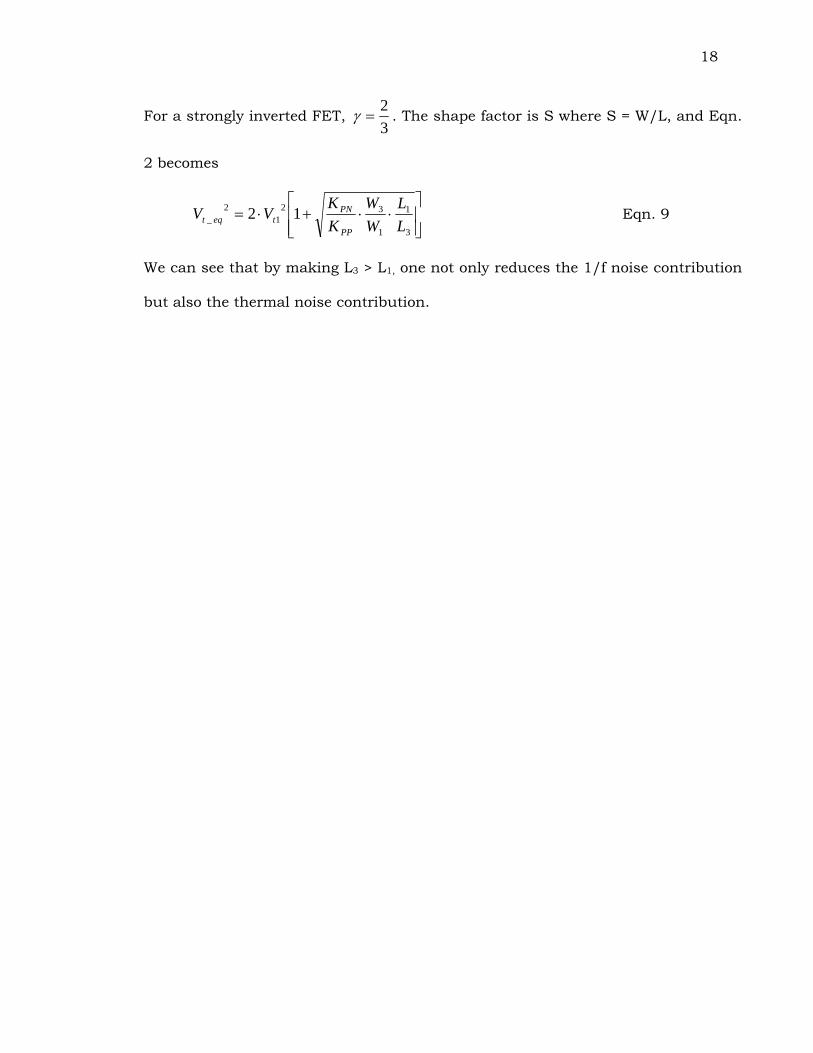
For a strongly inverted FET, 32
=γ . The shape factor is S where S = W/L, and Eqn.
2 becomes
⎥⎥⎦
⎤
⎢⎢⎣
⎡⋅⋅+⋅=
3
1
1
321
2_ 12
LL
WW
KK
VVPP
PNteqt Eqn. 9
We can see that by making L3 > L1, one not only reduces the 1/f noise contribution
but also the thermal noise contribution.
19
Noise Analysis
The main concern in our design is to minimize the noise contribution of the
op-amp while keeping the area occupied and the power consumption small.
MathCAD® was used to carry out the analysis of circuit performance. The
MathCAD file, given in Appendix A, contains all the necessary theoretical
calculations and related equations. The MathCAD design sheet allows one to
compute the total input-referred noise of the amplifier with and without
“chopping”. It was also used to predict theoretically achievable SNR values. Also,
coefficients needed for noise generation (thermal and 1/f) for use in MATLAB
simulations were computed using the design sheet. At the onset, some
assumptions were made [Mor:10]. These include
o The gain of the chopper amplifier would be set by the capacitor ratio C1/C2.
The gain needs to be chosen large enough so that the noise of succeeding
electronic stages, the anti-aliasing filter and the analog-to-digital converter
(ADC), when referred to the input is to be negligible. However, the area of
the pre-amplifier increases as the gain is raised because the capacitor ratio
must be increased. Furthermore, while the EcoG signals are very small, the
electrode signals are frequently accompanied by common-mode signals (60
Hz pick-up, for example). As we shall show in a later section of this thesis,
because of mismatches in the impedance of the electrodes, a common-mode
signal can be converted into a differential signal. It is important that the
ADC not saturate if the 60 Hz interference, for example, is to be removed
using digital filtering techniques as we certainly plan on doing. It is for
these reasons that a gain of 50 (34 dB) was settled upon. In reality the
20
“effective gain” of the chopper amplifier is about 35 (31 dB). The loss in gain
is due to the “chopping action” as described earlier.
o A minimum input signal level (from the electrodes) of 1 µV peak-to-peak is
expected. This fact is based on discussions with Dr. Moran at Washington
University in Saint Louis.
o The chopper frequency is to be fch = 16 kHz. As explained earlier, choice of
this chopping frequency is a good compromise between reducing 1/f noise
and maintaining low power consumption.
o The amplifier bandwidth is chosen to be twice the chopping frequency or 32
kHz. As explained in an earlier section, this helps reduce artifacts which are
a result of the “chopping” while incurring a gain loss of only 3 dB.
o The bandwidth (BW) of interest in the proposed application is from 75Hz to
105 Hz. The EcoG signals are the result of the firing a very large number of
neurons in the area of the brain which is related to the activity that the
subject wishes to perform. Very high firing rates are less probable than
lower firing rates so power spectral densities associated with neural activity
tend to exhibit a 1/f characteristic. Increasing the bandwidth much above
105 Hz does little to improve SNR. Moreover, considering frequencies much
below 75 Hz is not productive because of the 60 Hz pick-up issues discussed
above. Since the bandwidth of interest is so narrow (only 30 Hz!), we opted
to test the chopper with a single-frequency, namely, a sinusoid at 90 Hz.
o A signal-to-noise ratio (SNR) of at least 6 dB is needed when a 90 sine-wave
test signal is applied to the amplifier. While on the surface such a low
acceptable SNR appears troublesome, this in not the case. In the proposed
BCI application, the researchers are looking for gross changes in brain
21
activity. We will briefly explain the extraction algorithm used in the
proposed BCI. The output of the ADC is applied to a band-pass filter (75 –
105 Hz). The output of this band-pass filter is then rectified and passed
through a low-pass filter, thereby implementing an energy measure. This
energy estimate is then simply compared against a threshold. Estimates of
the neural energy above threshold are deemed “interesting”, those below are
considered “not interesting”. Hence, one can see that the need for high SNR
does not really exist.
o A power supply of 3.6 V must be used. This was a constraint requested by
Dr. Moran. The reasons for 3.6 V operation of the ASIC are beyond the
scope of this thesis.
Using the information presented above, the chopper’s total allowable noise,
Ntot, was computed using VAA prms710536.3
21
21 −×=⋅⋅= and the minimum SNRdB
value of 6 dB, in the equation presented below
⎟⎟⎠
⎞⎜⎜⎝
⎛⋅=
tot
rmsdB N
ASNR 10log20 . Eqn. 10
The result was Ntot should not exceed 180 n V.
The analysis consists of (1) sizing the input and load devices, (2) computing
the total equivalent input-referred noise of the core amplifier, and (3) computing
the SNR value to make sure that the noise specification is satisfied. This was
followed by sizing the remainder of the transistors of the OTA to obtain an estimate
of the area occupied and the power likely to be consumed.
22
To find the minimum value of the input transconductance, gmi, which is
governed by noise considerations, we allotted half of the total noise power to the
thermal noise contribution and the other half to the flicker noise contribution i.e.
nVN
NN totft 127
2=== .
In the equation below which predicts thermal noise (Eqn. 11) [All:03], the
thermal resistance of the input devices, R, was taken as mig
R 1322 ⋅⋅= . Eqn. 11
predicts the thermal noise voltage and in Eqn. 12 we solve for the minimal input
device transconductance which must be achieved.
BWRUqN Tet ⋅⋅⋅⋅= 4 Eqn. 11
2min_ 316
t
Temi N
BWUqg
⋅
⋅⋅⋅= Eqn. 12
The result was Ω
×= − 110265.4 5min_mig .
To compute the noise contribution of the input devices, the differential tail
current was chosen to be Ib = 5 µA. The shape factor of the input devices was then
computed using
θ⋅⋅⋅
=nUK
I
STPP
b
.22
21 Eqn. 13
where θ is the inversion coefficient, chosen to be equal to 1.
23
From the value of the shape factor, the width was computed after choosing a
value for the length (S1 = W1/L1). The input transconductance was then computed
using the equation
n
IKSg DSPP
m⋅⋅⋅
= 11
2 Eqn. 14
and the result was Ω
×= − 110341.4 51mg , which is greater than the minimum value,
gmi_min. After that, the value of gm1 was used to compute the thermal noise
contribution of the input devices using the equation
BWg
UqVm
Tet ⋅⎟⎟⎠
⎞⎜⎜⎝
⎛⋅⋅⋅⋅⋅=
11
13224 Eqn. 15
The 1/f noise contribution considering both cases, without and with the
“chopping”, was computed using the following equations:
⎟⎟⎟⎟
⎠
⎞
⎜⎜⎜⎜
⎝
⎛
−
+⋅
⋅⋅=
2
2ln.
20
0
11_1 BWf
BWf
LWCKvPV
oxnoChopf Eqn. 16
⎟⎟⎟⎟
⎠
⎞
⎜⎜⎜⎜
⎝
⎛
−+
++⋅
⋅⋅=
2
2ln.
20
0
11_1 BWff
BWff
LWCKvPV
chop
chop
oxChopf . Eqn. 17
The value for f0 in Eqn. 16 and Eqn. 17 is 90 Hz while the value for BW is 30 Hz.
To compute the noise contribution of the load devices, the transconductance
was chosen to be as small as possible by making its length much greater than the
length of the input device i.e. L3> L1. The transconductance of the load device is
given by
24
n
IKSg DSPN
m⋅⋅⋅
= 33
2. Eqn. 18
The thermal noise and the 1/f noise contributions “without” and “with” the
chopper for the load devices were computed using the following equations:
BWg
UqVm
Tet ⋅⎟⎟⎠
⎞⎜⎜⎝
⎛⋅⋅⋅⋅⋅=
33
13224 Eqn. 19
⎟⎟⎟⎟
⎠
⎞
⎜⎜⎜⎜
⎝
⎛
−
+⋅
⋅⋅=
2
2ln.
20
0
33_3 BWf
BWf
LWCKvNV
oxnoChopf Eqn. 20
⎟⎟⎟⎟
⎠
⎞
⎜⎜⎜⎜
⎝
⎛
−+
++⋅
⋅⋅=
2
2ln.
20
0
33_3 BWff
BWff
LWCKvPV
chop
chop
oxChopf . Eqn. 21
For the input devices, the total noise contributions, “without” and “with” the
chopper respectively, were computed using
2_1
21_1 noChopftnoChop VVV += Eqn. 22
and
2_1
21_1 ChopftChop VVV += . Eqn. 23
For the load devices, the total noise contributions, “without” and “with” the
chopper respectively, were first computed using
2_3
23_3 noChopftnoChop VVV += Eqn. 24
and
2_3
23_3 ChopftChop VVV += . Eqn. 25
25
The input-referred noise of the load devices, “without” and “with” the chopper
respectively, were computed using
g
noChopnoChopeq R
VV _3
_3 = Eqn. 26
and
g
ChopChopeq R
VV _3
_3 = . Eqn. 27
where 3
1
m
mg g
gR = .
Finally the total input referred noise of the OTA, “without” and “with” the chopper
respectively, were computed using
2_3
2_1_ noChopeqnoChopnoChopeq VVV += Eqn. 28
2_3
2_1_ ChopeqChopChopeq VVV += Eqn. 29
In addition to the computation of the total equivalent input-referred noise of
the OTA, four parameters needed to generate accurate time-domain noise
waveforms for use in the MATLAB® simulations of the chopper amplifier (to be
discussed in the following chapter of this thesis) were computed. The thermal
resistances of the input and load devices are given by
BWUq
VR
Te
tnp ⋅⋅⋅
=4
21 Eqn. 30
and
2
23
4 gTe
tnn RBWUq
VR
⋅⋅⋅⋅= Eqn. 31
26
while the flicker noise parameters for both devices are given by
11 LWC
KvPKox
fp ⋅⋅= Eqn. 32
and
233 gox
fn RLWCKvNK
⋅⋅⋅= . Eqn. 33
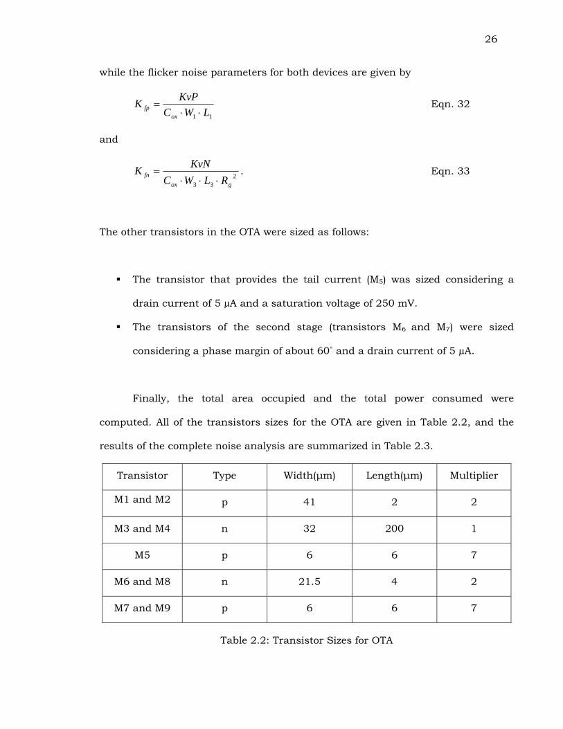
The other transistors in the OTA were sized as follows:
The transistor that provides the tail current (M5) was sized considering a
drain current of 5 µA and a saturation voltage of 250 mV.
The transistors of the second stage (transistors M6 and M7) were sized
considering a phase margin of about 60˚ and a drain current of 5 µA.
Finally, the total area occupied and the total power consumed were
computed. All of the transistors sizes for the OTA are given in Table 2.2, and the
results of the complete noise analysis are summarized in Table 2.3.
Transistor Type Width(μm) Length(μm) Multiplier
M1 and M2
p 41 2 2
M3 and M4 n 32 200 1
M5 p 6 6 7
M6 and M8 n 21.5 4 2
M7 and M9 p 6 6 7
Table 2.2: Transistor Sizes for OTA
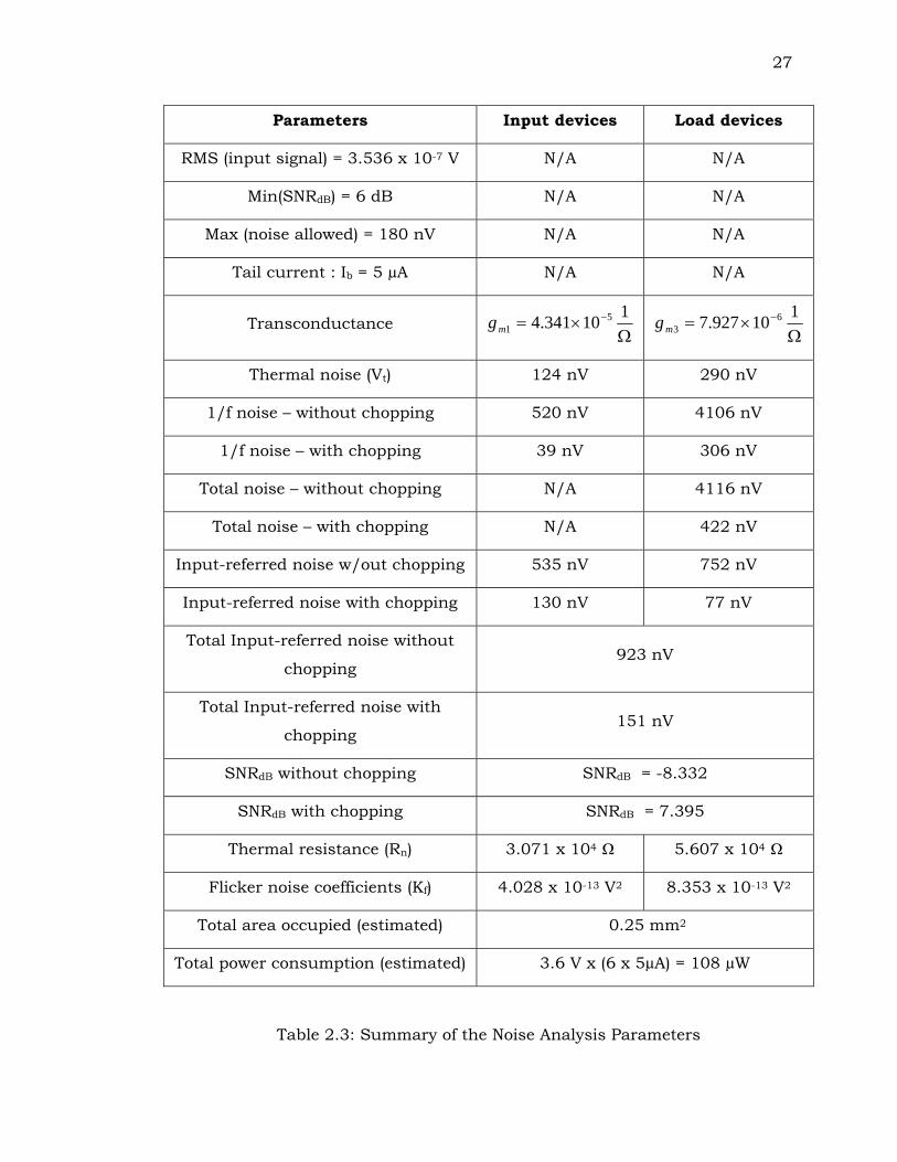
27
Parameters Input devices Load devices
RMS (input signal) = 3.536 x 10⁻⁷ V N/A N/A
Min(SNRdB) = 6 dB N/A N/A
Max (noise allowed) = 180 nV N/A N/A
Tail current : Ib = 5 µA N/A N/A
Transconductance Ω
×= − 110341.4 51mg
Ω×= − 110927.7 6
3mg
Thermal noise (Vt) 124 nV 290 nV
1/f noise – without chopping 520 nV 4106 nV
1/f noise – with chopping 39 nV 306 nV
Total noise – without chopping N/A 4116 nV
Total noise – with chopping N/A 422 nV
Input-referred noise w/out chopping 535 nV 752 nV
Input-referred noise with chopping 130 nV 77 nV
Total Input-referred noise without
chopping 923 nV
Total Input-referred noise with
chopping 151 nV
SNRdB without chopping SNRdB = -8.332
SNRdB with chopping SNRdB = 7.395
Thermal resistance (Rn) 3.071 x 10⁴ Ω 5.607 x 10⁴ Ω
Flicker noise coefficients (Kf) 4.028 x 10⁻¹³ V2 8.353 x 10⁻¹³ V2
Total area occupied (estimated) 0.25 mm2
Total power consumption (estimated) 3.6 V x (6 x 5µA) = 108 µW
Table 2.3: Summary of the Noise Analysis Parameters
28
CHAPTER 3
SYSTEM LEVEL SIMULATION
Introduction
This chapter is dedicated to the simulation of the chopper amplifier at the
system level using MATLAB®. The signal flow diagram for the chopper amplifier is
illustrated in Figure 3.1. The chapter is divided into two parts. The first part
presents an overview of the MATLAB® code that was written to analyze the
performance of chopper amplifier and a brief description of each MATLAB®
function used in the simulation, and the second part covers circuit performance
and simulation results.
MATLAB® Code Description
A main routine, called “ChopperTool”, was developed using MATLAB® to
analyze the performance of the chopper amplifier. A listing of all of the MATLAB®
code that was developed is included in Appendix B. The main routine,
“ChopperTool”, is used to compute the SNR value of the output of the chopper
amplifier. It addition, it is used to plot the time domain and the frequency domain
waveforms of the outputs. “ChopperTool” calls many other functions; they are:
The SineWaveGenerator function that generates a sine wave with user-
specified frequency and peak amplitude.
The SquareWaveGenerator function that generates a square wave, with user-
specified frequency and peak amplitude. It is used to modulate the input
29
signal to the chopper frequency and again to demodulate the signal to base-
band after amplification.
The HighPass function which implements a high-pass filter to set the lower
frequency corner of the amplifier to 1Hz.
The NoiseGenerator function that generates a noise vector comprised of both
white and flicker noise components.
The LowPass function which implements a low-pass filter to set the higher
frequency corner of the amplifier to 32 kHz.
For simulation purposes, the main routine calls other functions which are not part
of the chopper amplifier; they are:
The AAF function which implements a 2nd order low-pass filter, with a
corner frequency of 12 kHz that provides anti-aliasing and also removes
“chopping” artifacts.
The BandPass function which is an 8th order band-pass filter (75Hz –
105Hz).
In order to compute the SNR (Signal-to-Noise-Ratio) of the chopper, the code
calls two other functions which are FFTmagnitude and ComputeSNR. The
FFTmagnitude function is used to compute the FFT of the outputs signal, and the
ComputeSNR function uses the results of the FFTmagnitude calculation to compute
the SNR of the output signal. Finally, ChopperTool calls the functions
TimeDomainPlot, and FreqDomainPlot to plot the time domain and frequency
domain waveforms.
30
Ana
log
Inpu
t
2ndor
der
AA
F
12kH
zcl
ock
Ant
i-A
liasi
ng F
ilter
Mod
ulat
orD
emod
ulat
or
16kH
zcl
ock
16kH
zcl
ock
f c=
32kH
z
Cho
pper
Am
plifi
er
Ana
log
HPF
Pure
A
mpl
ifica
tion
Ana
log
LPF
+
f c=
1Hz
Gai
n =
50N
oise
The
Am
plifi
er
8nd o
rder
B
PF
[75H
z –
105H
z]
Ban
d-Pa
ss F
ilter
Figu
re 3
.1:
Sig
nal
Flo
w D
iagr
am fo
r a
Mat
lab
Sim
ula
tion
of t
he
Cho
pper
Am
plifi
er
31
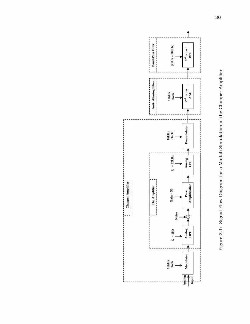
The signal-flow diagram, illustrated in Figure-3.1, contains three blocks: the
chopper amplifier, the anti-aliasing filter, and the band-pass filter. The input signal
is a 90Hz sine wave generated by the SineWaveGenerator function.
The Chopper Amplifier contains three modules: the Modulator, the Amplifier,
and the Demodulator. The Modulator and Demodulator are implemented by a
simple square wave generated by the function SquarewaveGenerator. It is used to
modulate the input signal to the chopping frequency (16 kHz). The same function
is called to demodulate the signal at the output of the amplifier.
The Amplifier is implemented by a cascade of a high-pass filter module that
sets the lower corner of amplifier bandwidth to 1Hz, a pure amplification by a
factor of 50, and a low-pass filter function that sets the upper corner frequency of
the amplifier (32 kHz).
The Anti-Aliasing Filter is a 2nd order LPF that is implemented by the AAF
function. The Band-Pass Filter is a band-pass filter implemented by the BandPass
function.
First, the analog input signal is modulated to a chopper frequency of 16kHz
using the modulator, after that the modulated signal go through the amplifier stage
where it undergoes a high-pass filtering of a frequency corner of 1Hz, a pure
amplification of a factor 50 with a noise added at the input, and then a low-pass
filtering with a frequency corner of 32 kHz. Finally, the signal is demodulated to
base-band using the same square-wave as used by the modulator.
Furthermore, the output signal of the chopper amplifier is filtered using a
second order low-pass filter (Anti-Aliasing Filter) to remove artifacts introduced by
the “chopping”, and for a simulation purposes the final output signal is filtered
32
using an 8th order analog band-pass filter. In the BCI application, this band-pass
filter would be implemented by a DSP block that follows the ADC.
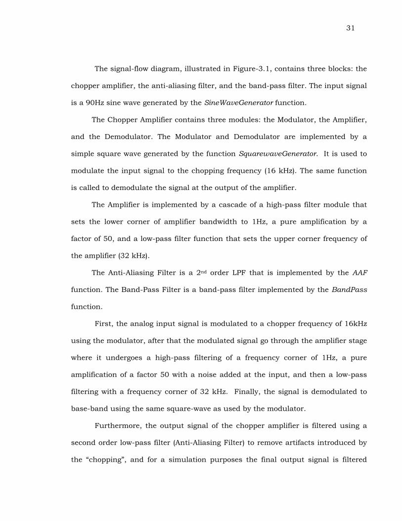
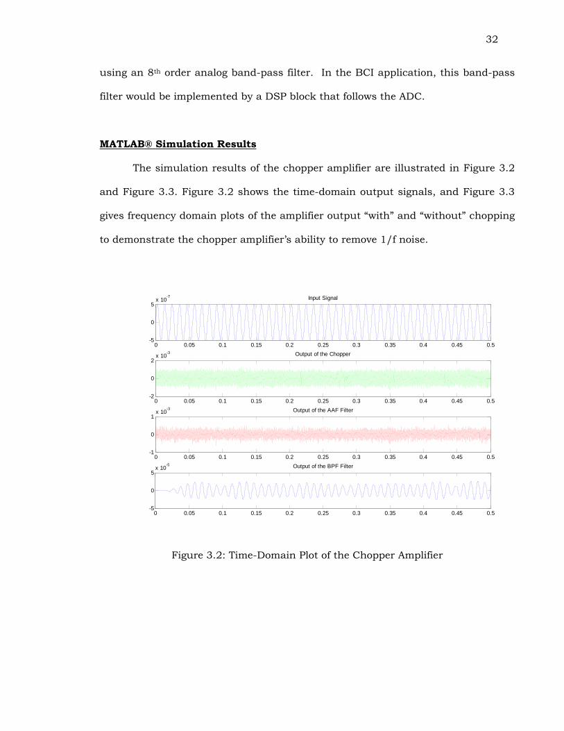
MATLAB® Simulation Results
The simulation results of the chopper amplifier are illustrated in Figure 3.2
and Figure 3.3. Figure 3.2 shows the time-domain output signals, and Figure 3.3
gives frequency domain plots of the amplifier output “with” and “without” chopping
to demonstrate the chopper amplifier’s ability to remove 1/f noise.
0 0.05 0.1 0.15 0.2 0.25 0.3 0.35 0.4 0.45 0.5-5
0
5x 10
-7 Input Signal
0 0.05 0.1 0.15 0.2 0.25 0.3 0.35 0.4 0.45 0.5-2
0
2x 10⁻³ Output of the Chopper
0 0.05 0.1 0.15 0.2 0.25 0.3 0.35 0.4 0.45 0.5-1
0
1x 10⁻³ Output of the AAF Filter
0 0.05 0.1 0.15 0.2 0.25 0.3 0.35 0.4 0.45 0.5-5
0
5x 10⁻⁵ Output of the BPF Filter
Figure 3.2: Time-Domain Plot of the Chopper Amplifier
33
60 70 80 90 100 110 120-150
-140
-130
-120
-110
-100
-90
-80
-70
Frequency - Hz
Spectrum of the Amplifier wth and without the Chopper
with Chopperwithout Chopper
Figure 3.3: Frequency-Domain Plot of the Amplifier With and Without Chopping
In Figure 3.2, we can see that the signal was cleaned up from the artifacts
and noise after the band-pass filter. Figure 3.3 shows that the chopper causes
about a 3 dB decrease in the gain but it introduces about 15 to 16 dB decrease in
the noise which increases the SNR by the same amount.
The SNR values at the output of the amplifier, for both cases, were
computed using the ComputeSNR function, and the results were -6.5 dB and 8.0
dB “without” and “with” a chopper, respectively. Compared to the values computed
using MathCAD® (-8.3 dB and 7.4 dB) we can see that the values computed using
MATLAB compare favorably with the theoretical values predicted by our
MathCAD® design sheet.
34
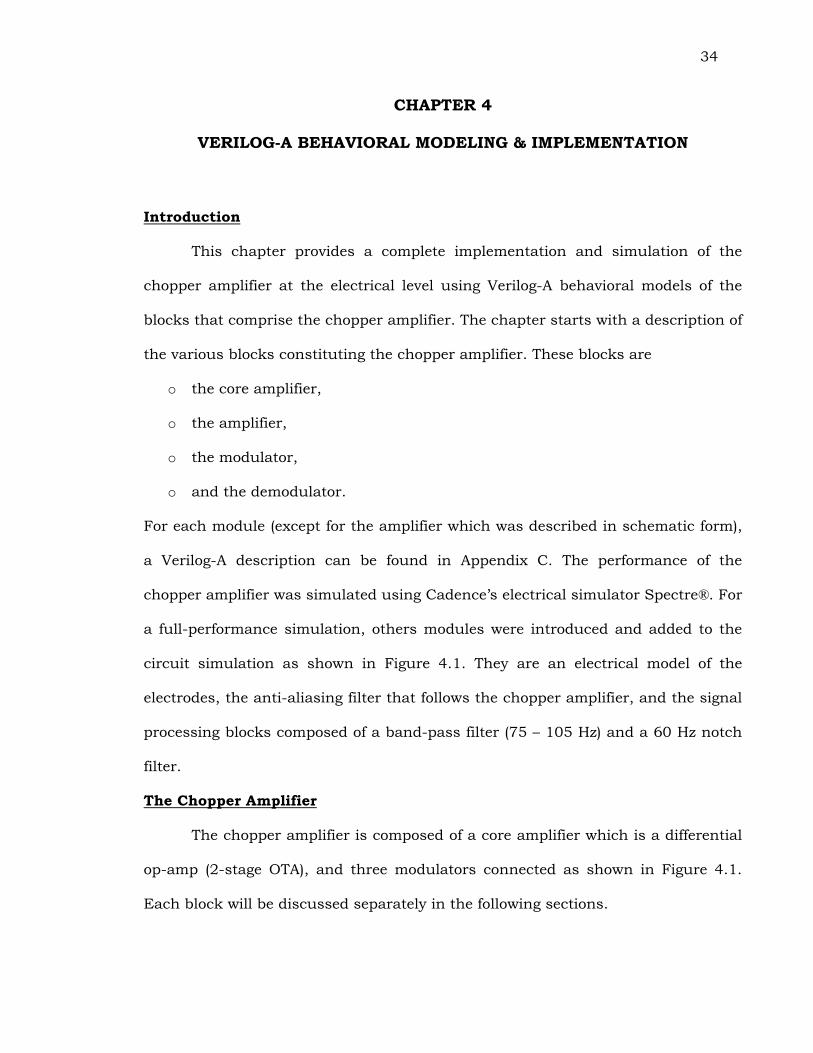
CHAPTER 4
VERILOG-A BEHAVIORAL MODELING & IMPLEMENTATION
Introduction
This chapter provides a complete implementation and simulation of the
chopper amplifier at the electrical level using Verilog-A behavioral models of the
blocks that comprise the chopper amplifier. The chapter starts with a description of
the various blocks constituting the chopper amplifier. These blocks are
o the core amplifier,
o the amplifier,
o the modulator,
o and the demodulator.
For each module (except for the amplifier which was described in schematic form),
a Verilog-A description can be found in Appendix C. The performance of the
chopper amplifier was simulated using Cadence’s electrical simulator Spectre®. For
a full-performance simulation, others modules were introduced and added to the
circuit simulation as shown in Figure 4.1. They are an electrical model of the
electrodes, the anti-aliasing filter that follows the chopper amplifier, and the signal
processing blocks composed of a band-pass filter (75 – 105 Hz) and a 60 Hz notch
filter.
The Chopper Amplifier
The chopper amplifier is composed of a core amplifier which is a differential
op-amp (2-stage OTA), and three modulators connected as shown in Figure 4.1.
Each block will be discussed separately in the following sections.
35
Sig
nal P
roce
ssin
g B
lock
4th
orde
r
SB
F55
hz -
65H
z
Anal
og N
otch
Fi
lter (
60H
z)
8thor
der
BP
F75
hz -
105H
z
Anal
og B
and-
pass
Fi
lter (
90H
z)
AA
FG
ain
= 5
fc =
12k
Hz
Ant
i-Alia
sing
Fi
lter
Cho
pper
Am
plifi
er
Figu
re 4
.1: B
lock
Dia
gram
for S
imul
atio
n of
the
Cho
pper
Am
plifi
er a
t the
Ele
ctric
al L
evel
Ele
ctro
des
-+Vid/
2
Vid/
2
+ -
Vcm
+ -
Prob
e-1
Prob
e-2
Pseu
do-r
esis
tor
C2
Pseu
do-r
esis
tor
C2
-+
Noi
se fi
le
CI
CI
MO
D1
f.ch
MO
D2
f.ch
MO
D3
f.ch
_ +
+ _
Op-
Amp
36
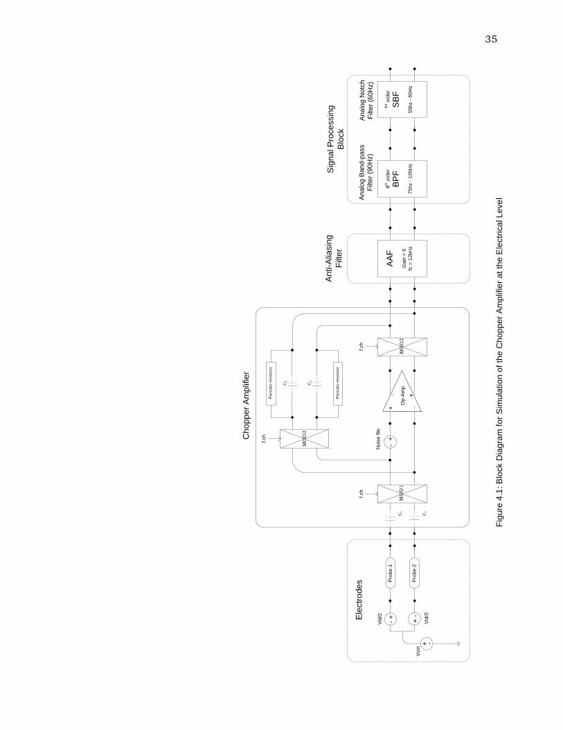
Fully differential op-amp
A Verilog-A description of the fully differential op-amp is located in Appendix
C. The open-loop gain of the amplifier was set to 10,000 (or 80dB) and the gain-
bandwidth (GBW) product to 1.6 MHz. Since the close-loop gain of the amplifier
was chosen as 50 (as explained earlier), a GBW of 1.6 MHz results in a closed-loop
bandwidth of a 32 kHz (i.e. twice the chopping frequency) as was stated in an
earlier section of this thesis.
The performance of the op-amp was simulated by running an AC analysis.
The bode plot of one output of the op-amp is shown in Figure 4.2.
Figure 4.2: Bode Plot of the Op-Amp
The open-loop gain is 74 dB which corresponds to a factor of 5000. This is
half of the open-loop gain for the fully-differential amplifier (i.e. 10,000) since we
are looking at just one output. Also, by examining the plot we observe that the
37
GBW is 1.6 MHz (one again because we are looking at single output one needs to
look at where the gain is -6 dB rather than the traditional 0 dB value).
The amplifier
Different candidate amplifiers are illustrated in Figure 4.3.
_
+
+
_
Op-Amp
Pseudo-resistor
C2
Pseudo-resistor
C2
CI
CI
IN+
IN-
OUT+
OUT-
a) b)
_
+
+
_
Op-Amp
C2
C2
CI
CI
IN+
IN-
OUT+
OUT- +
_
Op-Amp
C2
CI
CI
IN+
IN-OUT+
C2
c) d)
+
_
Op-AmpCI
CI
IN+
IN-OUT+
C2
Real resistor
C2
Real resistor
Figure 4.3: Different Candidate Amplifiers: a) Fully-Differential Implementation, b)
Single-Ended Using Real Resistors, c) Fully-Differential Using Diode-Connected
pFETs, d) Single-Ended Using Diode-Connected pFETs.
38
The circuit of Fig. 4c was ultimately selected as the best one for use in this
application because it is fully-differential (superior common-mode rejection!) and
because it uses a transistor’s off-resistance for DC feedback stabilization. The use
of a real resistor for DC feedback stabilization is no feasible in this application
because of the desired 1 Hz lower corner frequency.
The closed-loop gain of the amplifier is chosen to be 50. It is set by the ratio
of C1/C2. The resistors values are chosen to set the lower corner of the amplifier
around 1Hz. Because of this low frequency, the resistors values are too big (640
GΩ) for a feedback capacitor value, C2, of 0.25pF. It would occupy tremendous
area and thus is impossible to incorporate onto the chip. To remedy this problem,
we replace the resistors with a diode-connected pFETs transistors ([Har:03]).
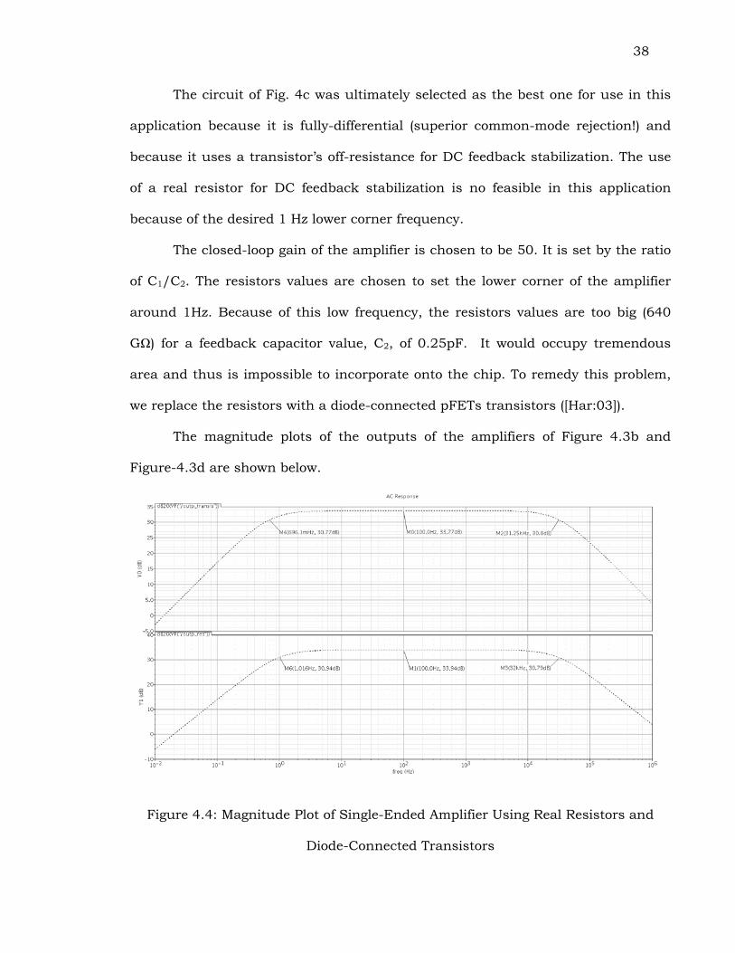
The magnitude plots of the outputs of the amplifiers of Figure 4.3b and
Figure-4.3d are shown below.
Figure 4.4: Magnitude Plot of Single-Ended Amplifier Using Real Resistors and
Diode-Connected Transistors
39
From the plots, one can easily see that the closed-loop gain is indeed 35 dB
(i.e. 50). The lower corner and the high corner frequencies are 1Hz and 32 kHz for
the amplifier using real resistors, and 0.7 Hz and 32 kHz respectively when using
diode-connected FETs.
To demonstrate the importance of substituting the real resistors with a
diode-connected FETs (in addition to area considerations) we ran transient
simulations for both amplifiers of Figure 4.3b and Figure 4.3d using both a small
disturbance (10mV) and a large disturbance (500mV) at the inputs of the
amplifiers, and we observed the output responses presented in Figures 4.5 and
4.6.
Figure 4.5: Transient Response of Amplifier for a 10mV Disturbance: (a) Using Real
Resistors, (b) Using Diode-Connected FETs.
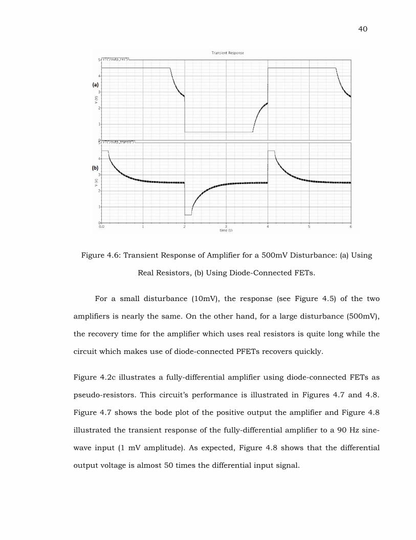
40
Figure 4.6: Transient Response of Amplifier for a 500mV Disturbance: (a) Using
Real Resistors, (b) Using Diode-Connected FETs.
For a small disturbance (10mV), the response (see Figure 4.5) of the two
amplifiers is nearly the same. On the other hand, for a large disturbance (500mV),
the recovery time for the amplifier which uses real resistors is quite long while the
circuit which makes use of diode-connected PFETs recovers quickly.
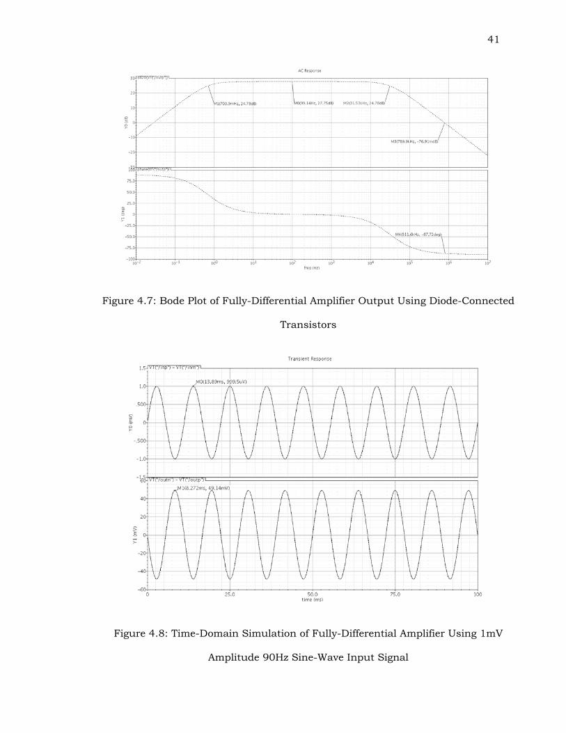
Figure 4.2c illustrates a fully-differential amplifier using diode-connected FETs as
pseudo-resistors. This circuit’s performance is illustrated in Figures 4.7 and 4.8.
Figure 4.7 shows the bode plot of the positive output the amplifier and Figure 4.8
illustrated the transient response of the fully-differential amplifier to a 90 Hz sine-
wave input (1 mV amplitude). As expected, Figure 4.8 shows that the differential
output voltage is almost 50 times the differential input signal.
41
Figure 4.7: Bode Plot of Fully-Differential Amplifier Output Using Diode-Connected
Transistors
Figure 4.8: Time-Domain Simulation of Fully-Differential Amplifier Using 1mV
Amplitude 90Hz Sine-Wave Input Signal
42
The modulators
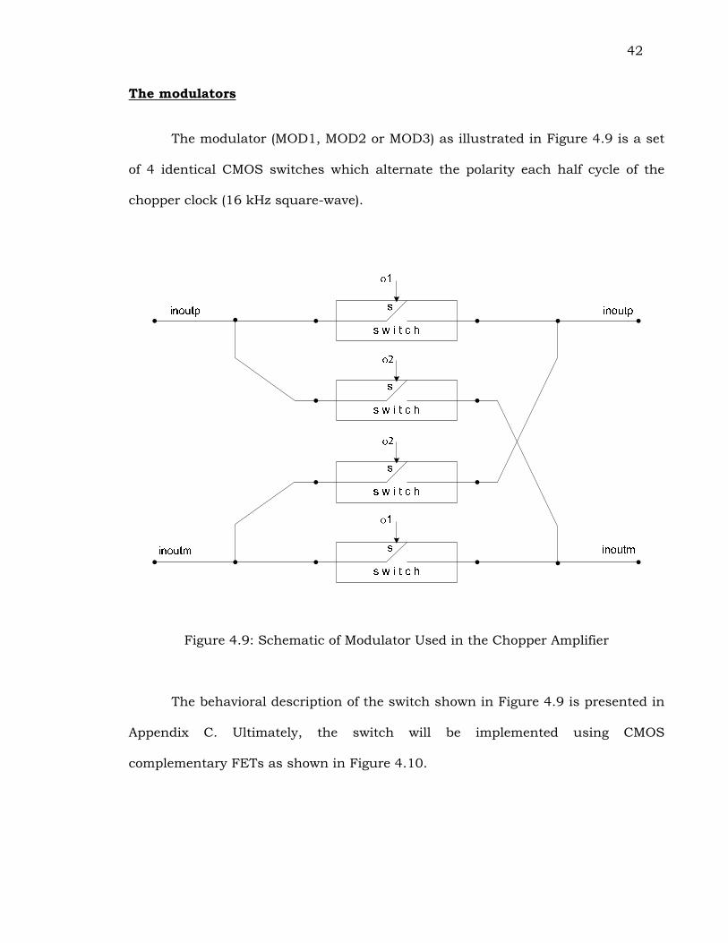
The modulator (MOD1, MOD2 or MOD3) as illustrated in Figure 4.9 is a set
of 4 identical CMOS switches which alternate the polarity each half cycle of the
chopper clock (16 kHz square-wave).
Figure 4.9: Schematic of Modulator Used in the Chopper Amplifier
The behavioral description of the switch shown in Figure 4.9 is presented in
Appendix C. Ultimately, the switch will be implemented using CMOS
complementary FETs as shown in Figure 4.10.
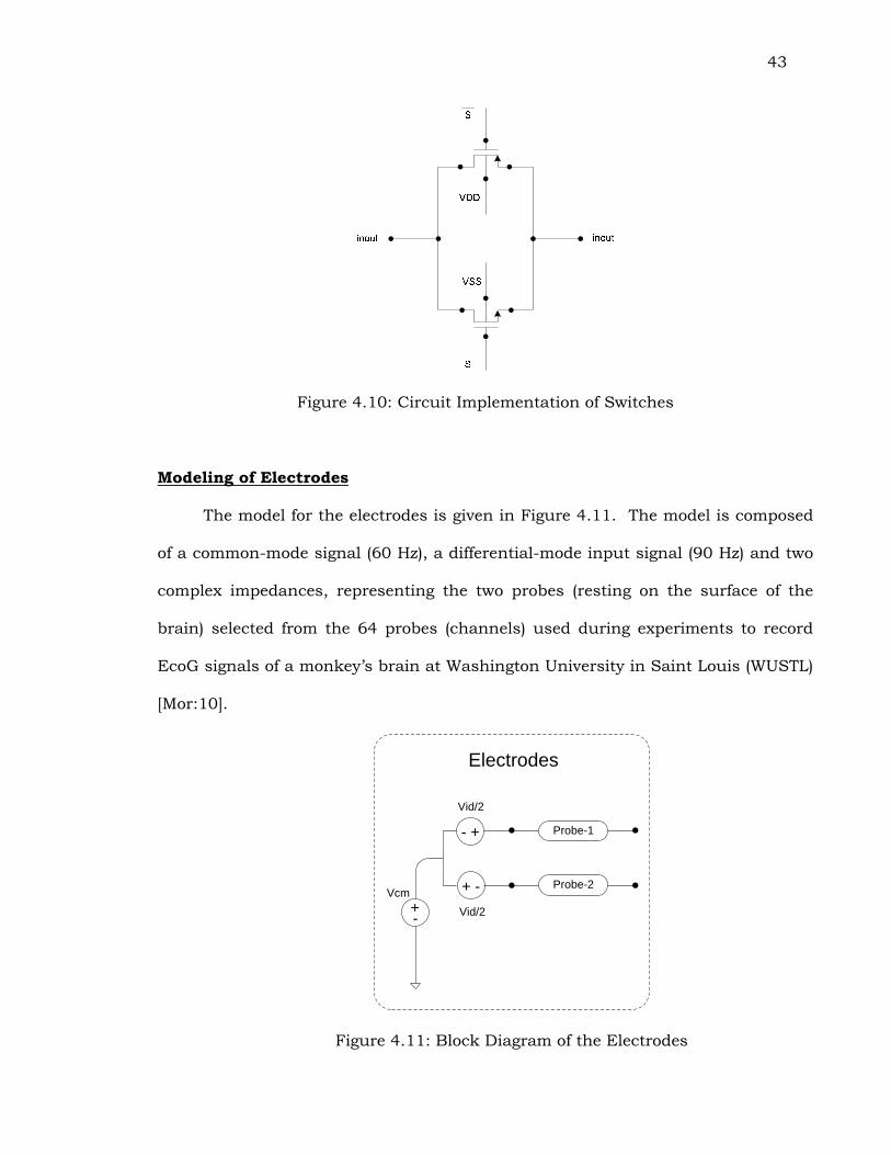
43
Figure 4.10: Circuit Implementation of Switches
Modeling of Electrodes
The model for the electrodes is given in Figure 4.11. The model is composed
of a common-mode signal (60 Hz), a differential-mode input signal (90 Hz) and two
complex impedances, representing the two probes (resting on the surface of the
brain) selected from the 64 probes (channels) used during experiments to record
EcoG signals of a monkey’s brain at Washington University in Saint Louis (WUSTL)
[Mor:10].
Electrodes
- +
Vid/2
Vid/2
+ -Vcm+-
Probe-1
Probe-2
Figure 4.11: Block Diagram of the Electrodes
44
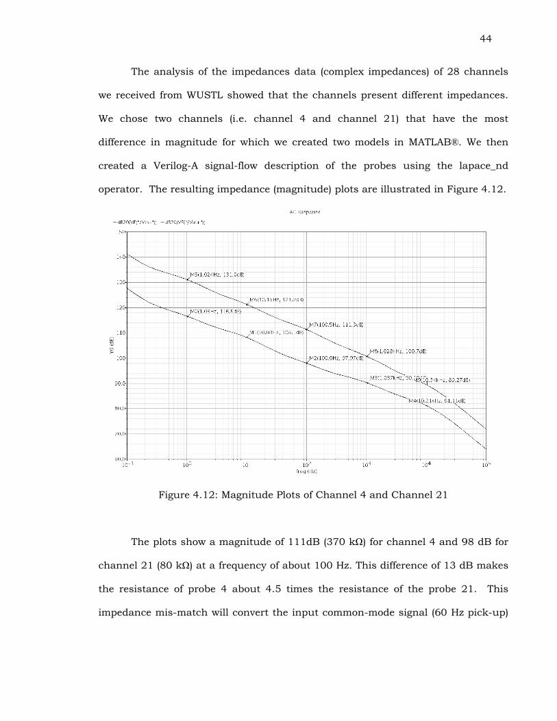
The analysis of the impedances data (complex impedances) of 28 channels
we received from WUSTL showed that the channels present different impedances.
We chose two channels (i.e. channel 4 and channel 21) that have the most
difference in magnitude for which we created two models in MATLAB®. We then
created a Verilog-A signal-flow description of the probes using the lapace_nd
operator. The resulting impedance (magnitude) plots are illustrated in Figure 4.12.
Figure 4.12: Magnitude Plots of Channel 4 and Channel 21
The plots show a magnitude of 111dB (370 kΩ) for channel 4 and 98 dB for
channel 21 (80 kΩ) at a frequency of about 100 Hz. This difference of 13 dB makes
the resistance of probe 4 about 4.5 times the resistance of the probe 21. This
impedance mis-match will convert the input common-mode signal (60 Hz pick-up)
45
to a differential signal at the output of the chopper amplifier; thus the need for a
notch filter to remove the common-mode signal.
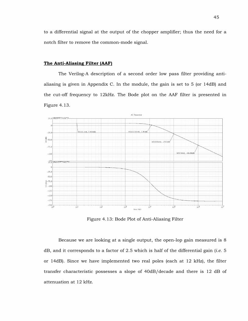
The Anti-Aliasing Filter (AAF)
The Verilog-A description of a second order low pass filter providing anti-
aliasing is given in Appendix C. In the module, the gain is set to 5 (or 14dB) and
the cut-off frequency to 12kHz. The Bode plot on the AAF filter is presented in
Figure 4.13.
Figure 4.13: Bode Plot of Anti-Aliasing Filter
Because we are looking at a single output, the open-lop gain measured is 8
dB, and it corresponds to a factor of 2.5 which is half of the differential gain (i.e. 5
or 14dB). Since we have implemented two real poles (each at 12 kHz), the filter
transfer characteristic possesses a slope of 40dB/decade and there is 12 dB of
attenuation at 12 kHz.
46
The Signal Processing Block
The signal processing block contains two filters: the band-pass filter and the
notch filter. Both filters are only for simulation purpose; they are analog filters
representing digital filters which are part of the DSP block following the ADC. The
band-pass filter is needed to band-limit the output from 75Hz – 107Hz, and the
notch filter is needed to remove the 60Hz common-mode signal picked up at the
input and converted to a differential signal due to a mismatch of the input
impedances.
The band-pass filter
Our band of interest is from 75Hz to 105Hz. Even after the anti-aliasing
filter with the corner frequency of 12kHz, the output signal still have some noise
and high frequency signals (artifacts of the “chopping”). The high-order band-pass
filter, designed considering our band of interest, will ensure a high quality output.
The Verilog-A description for an 8th order Band-Pass filter is given in Appendix C.
The magnitude plot is shown in Figure 4.14.
Figure 4.14: Magnitude Plot of the Band-Pass Filter
47
We notice that at 60Hz the attenuation is only about 30 dB which not enough to
adequately filter out the 60 Hz common-mode signal resulting from probe mis-
match, thus the need for the notch filter.
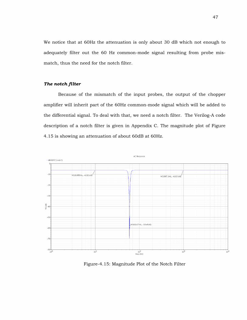
The notch filter
Because of the mismatch of the input probes, the output of the chopper
amplifier will inherit part of the 60Hz common-mode signal which will be added to
the differential signal. To deal with that, we need a notch filter. The Verilog-A code
description of a notch filter is given in Appendix C. The magnitude plot of Figure
4.15 is showing an attenuation of about 60dB at 60Hz.
Figure-4.15: Magnitude Plot of the Notch Filter
48
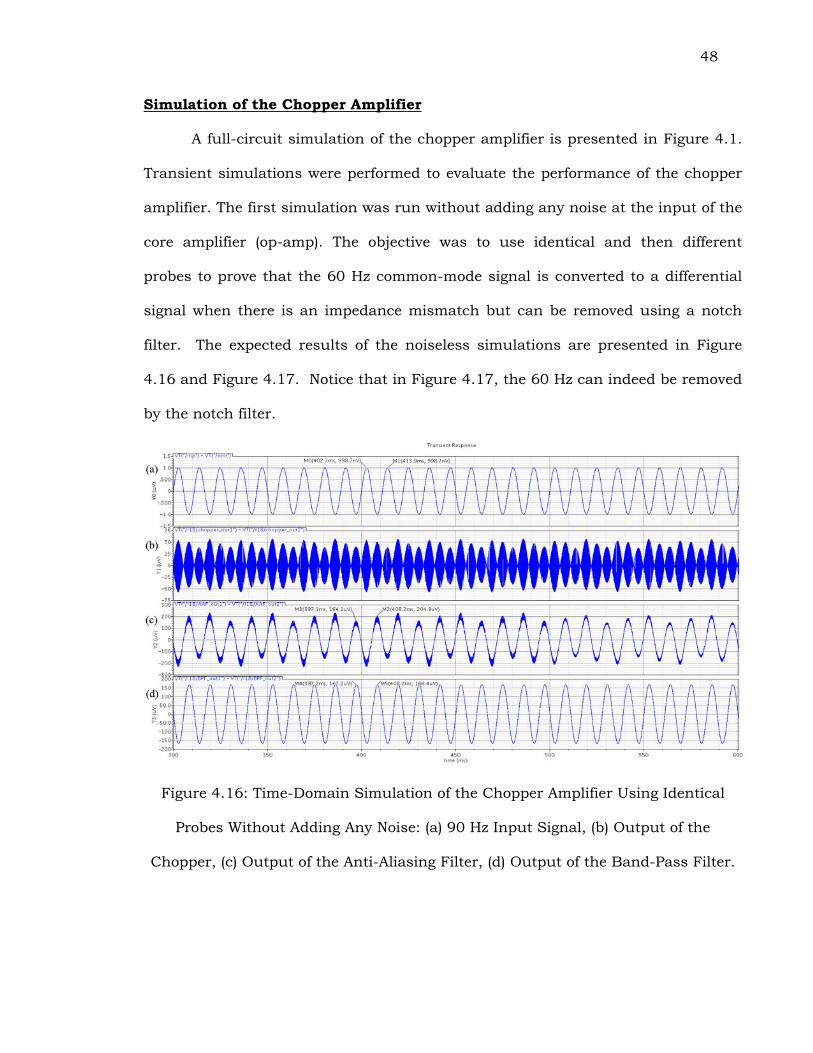
Simulation of the Chopper Amplifier
A full-circuit simulation of the chopper amplifier is presented in Figure 4.1.
Transient simulations were performed to evaluate the performance of the chopper
amplifier. The first simulation was run without adding any noise at the input of the
core amplifier (op-amp). The objective was to use identical and then different
probes to prove that the 60 Hz common-mode signal is converted to a differential
signal when there is an impedance mismatch but can be removed using a notch
filter. The expected results of the noiseless simulations are presented in Figure
4.16 and Figure 4.17. Notice that in Figure 4.17, the 60 Hz can indeed be removed
by the notch filter.
Figure 4.16: Time-Domain Simulation of the Chopper Amplifier Using Identical
Probes Without Adding Any Noise: (a) 90 Hz Input Signal, (b) Output of the
Chopper, (c) Output of the Anti-Aliasing Filter, (d) Output of the Band-Pass Filter.
49
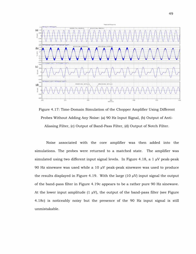
Figure 4.17: Time-Domain Simulation of the Chopper Amplifier Using Different
Probes Without Adding Any Noise: (a) 90 Hz Input Signal, (b) Output of Anti-
Aliasing Filter, (c) Output of Band-Pass Filter, (d) Output of Notch Filter.
Noise associated with the core amplifier was then added into the
simulations. The probes were returned to a matched state. The amplifier was
simulated using two different input signal levels. In Figure 4.18, a 1 µV peak-peak
90 Hz sinewave was used while a 10 µV peak-peak sinewave was used to produce
the results displayed in Figure 4.19. With the large (10 µV) input signal the output
of the band-pass filter in Figure 4.19c appears to be a rather pure 90 Hz sinewave.
At the lower input amplitude (1 µV), the output of the band-pass filter (see Figure
4.18c) is noticeably noisy but the presence of the 90 Hz input signal is still
unmistakable.
50
Figure 4.18: Time-Domain Simulation of the Chopper Amplifier Using Identical
Probes With Noise Added at the Input: (a) 1µV Peak-to-Peak 90 Hz Input Signal,
(b) Output of Anti-Aliasing Filter, (c) Output of Band-Pass Filter.
Figure 4.19: Time-Domain Simulation of the Chopper Amplifier Using Identical
Probes With Noise Added at the Input: (a) 10µV Peak-to-Peak 90 Hz Input Signal,
(b) Output of Anti-Aliasing Filter, (c) Output of Band-Pass Filter.
51
Finally, in Figures 4.20 and 4.21 we compare the output of the band-pass
filter when the chopper is driven with signal plus noise versus when the chopper is
driven by noise alone. In Figure 4.20, the input signal level is 1 V while in Figure
4.21, the input signal level is 10 V. This was done so that we could directly and
easily compute the SNR using time-domain data.
During the transient analysis, output data were recorded to a file and then
taken over into MATLAB for a SNR computation. The results were 10 dB for the
1µV peak-to-peak input signal and 28 dB for the 10µV peak-to-peak input signal.
These SNR values are in agreement with the theoretical computed values and the
MATLAB® simulation results.
Figure 4.20: Time-Domain Simulation of the Chopper Amplifier With Noise Added
at the Input: (a) Output of the Band-Pass Filter Using 1µV Peak-to-Peak 90 Hz
Input Signal, (b) Output of the Band-Pass Filter Without Input Signal.
52
Figure 4.21: Time-Domain Simulation of the Chopper Amplifier With Noise Added
at the Input: (a) Output of the Band-Pass Filter Using 10µV Peak-to-Peak 90 Hz
Input Signal, (b) Output of the Band-Pass Filter Without Input Signal.
53
CHAPTER 5
SUMMARY/FUTURE WORK
Summary
The thesis presented the design and simulation of a low-noise chopper
amplifier intended for use in the front-end of a single analog signal processing
channel that can be used in a multi-channel EcoG-based BCI system. The purpose
of this pre-amplifier is to amplify weak bioelectrical signals from passive electrodes
without introducing significant noise. The ON-Semiconductor 0.5 micron process
(C5N) is the target fabrication process. Like any CMOS process technology, it
possesses poor flicker (1/f) noise characteristics; therefore, designing a low-noise
amplifier is non-trivial. In this work, a chopper stabilization technique is used to
minimize the 1/f noise introduced by the core amplifier.
The amplifier proposed in this thesis uses the modulation technique to
transpose the signal to a higher frequency (16 kHz in this application) where there
is significantly less 1/f noise and then demodulates the signal back to baseband
after amplification while the inherent noise from the op-amp is modulated to the
chopping frequency. The chopper was implemented as a fully-differential circuit
with capacitive feedback along with pseudo-resistors for DC feedback stabilization.
A two-stage OTA serves as the core amplifier.
The work presented in this thesis began with a system-level analysis using
MathCAD®, followed by a system-level simulation using MATLAB®, and
culminated in an implementation at the electrical level (employing Verilog-A
behavioral models) using Cadence’s Spectre® simulator.
54
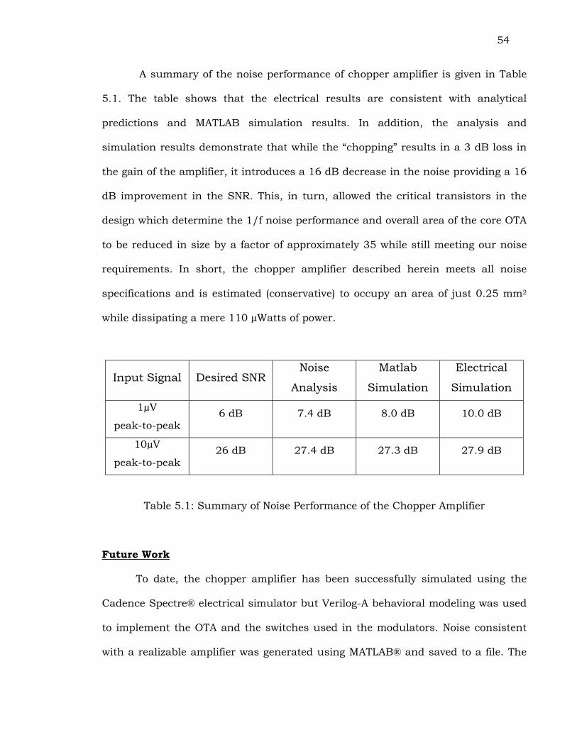
A summary of the noise performance of chopper amplifier is given in Table
5.1. The table shows that the electrical results are consistent with analytical
predictions and MATLAB simulation results. In addition, the analysis and
simulation results demonstrate that while the “chopping” results in a 3 dB loss in
the gain of the amplifier, it introduces a 16 dB decrease in the noise providing a 16
dB improvement in the SNR. This, in turn, allowed the critical transistors in the
design which determine the 1/f noise performance and overall area of the core OTA
to be reduced in size by a factor of approximately 35 while still meeting our noise
requirements. In short, the chopper amplifier described herein meets all noise
specifications and is estimated (conservative) to occupy an area of just 0.25 mm2
while dissipating a mere 110 µWatts of power.
Input Signal Desired SNR Noise
Analysis
Matlab
Simulation
Electrical
Simulation
1µV
peak-to-peak 6 dB 7.4 dB 8.0 dB 10.0 dB
10µV
peak-to-peak 26 dB 27.4 dB 27.3 dB 27.9 dB
Table 5.1: Summary of Noise Performance of the Chopper Amplifier
Future Work
To date, the chopper amplifier has been successfully simulated using the
Cadence Spectre® electrical simulator but Verilog-A behavioral modeling was used
to implement the OTA and the switches used in the modulators. Noise consistent
with a realizable amplifier was generated using MATLAB® and saved to a file. The
55
file was then played back in the simulator so that the chopper amplifier’s ability to
deal with the anticipated 1/f noise could be evaluated.
However, the core amplifier, the switches and the clock generator circuit of
the modulators must still be designed and tested at the transistor level. While the
critical transistors were sized and the bias currents selected so that appropriate
noise models could be developed, no simulations were carried out on the
transistor-level schematic per se.
The core amplifier consists of a two-stage OTA as shown in Figure 2-3 along
with a common-mode feedback circuit to control the common-mode output voltage.
The common-mode feedback circuits also still need to be designed and simulated.
The switches of the modulators can be implemented using CMOS complementary
FETs as shown in Figure 4.10. After extensive transistor-level simulations on the
chopper amplifier are performed, it must then be physically laid out and verified
against schematic.
Ultimately, the chopper amplifier must be combined with the anti-aliasing
filter and the Σ−Δ ADC to implement a single channel and finally integrated into a
multi-channel custom circuit that can be used for recording the signals from a
large array of electrodes. The ASIC may someday be fabricated in the ON-
Semiconductor 0.5 µm, double-poly (with high-resistance layer), tri-metal CMOS
process (C5N) and used in the EcoG-based BCI system currently under
development at Washington University in Saint Louis by Dr. Daniel Moran.
56
REFERENCES
[All:03] Phillip E. Allen and Douglas Holberg, “CMOS Analog Circuit Design:
Second Edition”, Oxford university Press, 2003. [Del:94] Tobi Delbrück & Carver A. Mead, “Analog VLSI Adaptive, Logarithmic,
Wide–Dynamic-Range Photoreceptor”, Dept. of Computation and Neural Systems, California Institute of Technology, 1994.
[Gra:01] Paul R. Gray, Paul J. Hurst, Stephen H. Lewis and Robert G. Meyer
“Analysis and Design of Analog Integrated Circuits” John Wiley and Sons, 2001
[Den:07] Tim Denison, Kelly Consoer, Wesley Santa, Al-Thaddeus Avestruz,
John Cooley, and Andy Kelly, “A 2uW 100 nV/sqrt(Hz) Chopper-Stabilized Instrumentation Amplifier for Chronic Measurement of Neural Field Potentials”, IEEE Journal of Solid-State Circuits, Vol. 42, No. 12, December 2007.
[Fit:04] Tony Fitzpatrick, “Thought Control: Human Subjects Play Real Mind
Games”, Washington University in St. Louis Record, Vol. 28, No. 35, June 2004.
[Han:07] Grani A. Hanasusanto, Yuanjin Zheng, “A Chopper Stabilized Pre-
amplifier for Biomedical Signal Acquisition”, 2007 IEEE International Symposium on Integrated Circuits (ISIC-2007).
[Har:03] Cameron T. Charles, Reid R. Harrison, “A Floating Gate Common
Mode Feedback Circuit for Low-Noise Amplifiers”, Southwest Symposium on Mixed Signal Design, 2003.
[Har:03] Reid R. Harrison and Cameron Charles, “A Low-Power Low-Noise
CMOS Amplifier for Neural Recording Applications”, IEEE Journal of Solid-State Circuits, Vol. 38, No. 6, June 2003.
[Leu:04] Eric C Leuthardt, Gerwin Schalk, Jonathan R. Wolpaw, Jeffrey G
Ojemann and Daniel W. Moran, “A brain–computer interface using electrocorticographic signals in humans”, Journal of Neural Engineering 1, 2004 (63-71).
[Mor:09] http://labs.seas.wustl.edu/bme/dmoran/ [Mor:10] Personal communication with Dr. Daniel Moran, Washington
University in Saint Louis. [Raz:01] Behzad Razavi, “Design of Analog CMOS Integrated Circuits”
McGraw-Hill, 2001.
57
[Sch:06] Andrew Schwartzm X. Tracy Cui, Douglas J. Weber, and Daniel Moran, “Brain-Controlled Interfaces: Movement Restoration with Neural Prosthetics”, Neuron 52, October 5, 2006 (205-220).
[Tem:96] Christian Enz and Gabor Temes, “Circuit Techniques for Reducing
the Effects of Op-Amp Imperfections: Autozeroing, Correlated Double Sampling, and Chopper Stabilization”, Proceedings of the IEEE, Vol. 84, No.11, November I996.
[Ter:04] Stephen C. Terry, Benjamin J. Blalock, James M. Rochell, M. Nance
Ericson, and Sam D. Caylor, “Time-Domain Noise Analysis of Linear Time-Invariant and Linear Time-Variant Systems Using MATLAB® and HSPICE”, 2004 IEEE
[Yos:05] Takeshi Yoshida, Yoshihiro Masui, Takayuki Mashimo, Mamoru
Sasaki and Atsushi Iwata, “A 1V Supply 50nV/sqrt(Hz) Noise PSD CMOS Amplifier Using Noise Reduction Technique of Autoz-eroing and Chopper Stabilization”, 2005 Symposium on VLSI Circuits Digest of Technical Papers.
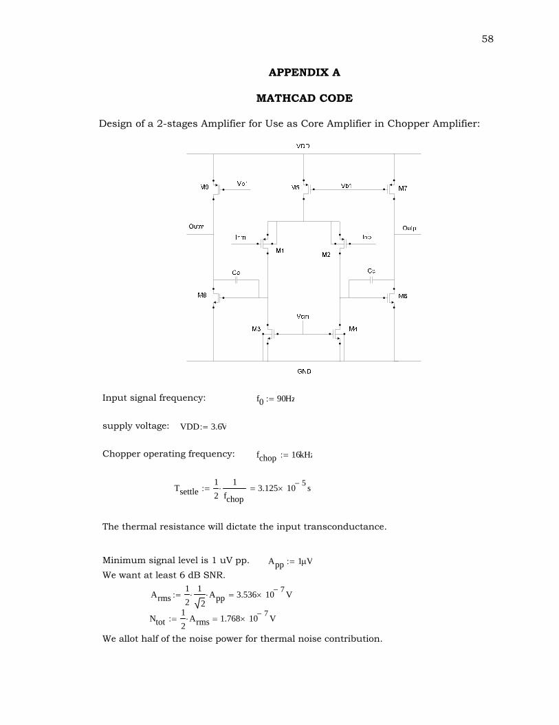
58
APPENDIX A
MATHCAD CODE
Design of a 2-stages Amplifier for Use as Core Amplifier in Chopper Amplifier:
Input signal frequency: f0 90Hz:=
supply voltage: VDD 3.6V:=
Chopper operating frequency: fchop 16kHz:=
Tsettle12
1fchop
⋅ 3.125 10 5−× s=:=
The thermal resistance will dictate the input transconductance.
Minimum signal level is 1 uV pp. App 1μV:=
Arms12
1
2⋅ App⋅ 3.536 10 7−
× V=:=
We want at least 6 dB SNR.
Ntot12
Arms⋅ 1.768 10 7−× V=:=
We allot half of the noise power for thermal noise contribution.
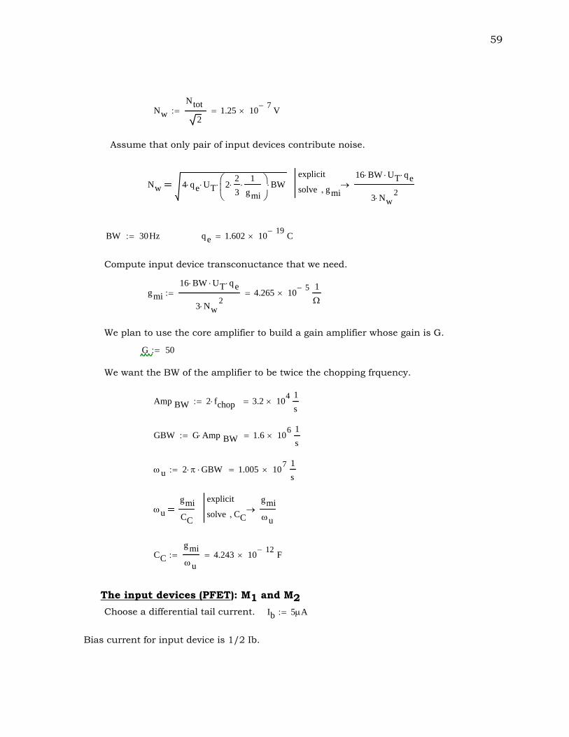
59
NwNtot
21.25 10 7−
× V=:=
Assume that only pair of input devices contribute noise.
Nw 4 qe⋅ UT⋅ 223
⋅1
gmi⋅⎛
⎜⎝
⎞⎟⎠
⋅ BW⋅explicit
solve gmi,
16 BW⋅ UT⋅ qe⋅
3 Nw2
⋅→
BW 30Hz:= qe 1.602 10 19−× C=
Compute input device transconuctance that we need.
gmi16 BW⋅ UT⋅ qe⋅
3 Nw2
⋅4.265 10 5−
×1Ω
=:=
We plan to use the core amplifier to build a gain amplifier whose gain is G.
G 50:=
We want the BW of the amplifier to be twice the chopping frquency.
Amp BW 2 fchop⋅ 3.2 104×
1s
=:=
GBW G Amp BW⋅ 1.6 106×
1s
=:=
ω u 2 π⋅ GBW⋅ 1.005 107×
1s
=:=
ωugmiCC
explicit
solve CC,
gmiωu
→
CCg miωu
4.243 10 12−× F=:=
The input devices (PFET): M1 and M2
Choose a differential tail current. Ib 5μA:=
Bias current for input device is 1/2 Ib.
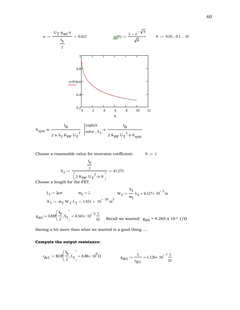
60
αUT g mi⋅ n⋅
Ib
2
0.621=:=
α θ( )1 e θ−
−
θ:=
θ 0.05 0.1, 10..:=
gds11
rds11.126 10 7−
×1Ω
=:=
0 2 4 6 8 10 120.2
0.4
0.6
0.8
1
α θ( )
θ
θsymIB
2 n⋅ S1⋅ KPP⋅ UT2
⋅
explicit
solve S1,
IB
2 KPP⋅ UT2
⋅ n⋅ θsym⋅→
Choose a reasonable value for inversion coefficient. θ 1:=
S1
Ib
2
2 KPP⋅ UT2
⋅ n⋅ θ⋅⎛⎝
⎞⎠
41.275=:=
Choose a length for the FET.
W1S1m1
L1⋅ 4.127 10 5−× m=:= m1 2:= L1 2μm:=
A 1 m1 W 1⋅ L1⋅ 1.651 10 10−× m2
=:=
gm1 GMPIb2
S1, ⎛⎜⎝
⎞⎟⎠
4.341 10 5−×
1Ω
=:= Recall we wanted: gmi = 4.265 x 10⁻⁵ 1/Ω
Having a bit more than what we wanted is a good thing ....
Compute the output resistance:
rds1 ROPIb2
L1, ⎛⎜⎝
⎞⎟⎠
8.88 106× Ω=:=
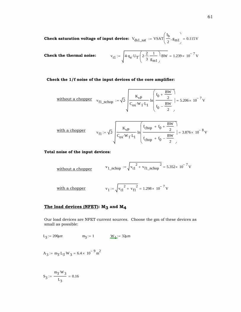
61
Vds1_sat VSATIb2
gm1, ⎛⎜⎝
⎞⎟⎠
0.115V=:= Check saturation voltage of input device:
Check the thermal noise: vt1 4 qe⋅ UT⋅ 223
⋅1
gm1⋅⎛
⎜⎝
⎞⎟⎠
⋅ BW⋅ 1.239 10 7−× V=:=
Check the 1/f noise of the input devices of the core amplifier:
without a chopper
with a chopper
Total noise of the input devices:
v1_nchop vt12 vf1_nchop
2+ 5.352 10 7−
× V=:= without a chopper
with a chopper v1 vt12 vf1
2+ 1.298 10 7−
× V=:=
vf1_nchop 2KvP
Cox W1⋅ L1⋅ln
f0BW
2+
f0BW
2−
⎛⎜⎜⎜⎝
⎞⎟⎟⎟⎠
⋅⋅ 5.206 10 7−× V=:=
vf1 2KvP
Cox W1⋅ L1⋅ln
fchop f0+BW
2+
fchop f0+BW
2−
⎛⎜⎜⎜⎝
⎞⎟⎟⎟⎠
⋅⋅ 3.876 10 8−× V=:=
The load devices (NFET): M3 and M4
Our load devices are NFET current sources. Choose the gm of these devices as small as possible:
W1 32μm:= m3 1:= L3 200μm:=
A3 m3 L3⋅ W 3⋅ 6.4 10 9−× m2
=:=
S3m3 W 3⋅
L30.16=:=
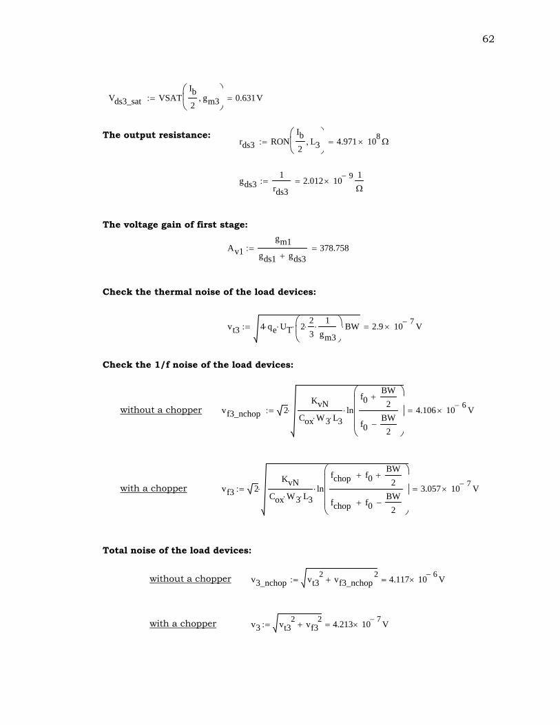
62
Vds3_sat VSATIb2
gm3, ⎛⎜⎝
⎞⎟⎠
0.631V=:=
The output resistance: rds3 RON
Ib2
L3, ⎛⎜⎝
⎞⎟⎠
4.971 108× Ω=:=
gds31
rds32.012 10 9−
×1Ω
=:=
The voltage gain of first stage:
Av1gm1
gds1 gds3+378.758=:=
Check the thermal noise of the load devices:
vt3 4 qe⋅ UT⋅ 223
⋅1
gm3⋅⎛
⎜⎝
⎞⎟⎠
⋅ BW⋅ 2.9 10 7−× V=:=
Check the 1/f noise of the load devices:
without a chopper vf3_nchop 2KvN
Cox W3⋅ L3⋅ln
f0BW
2+
f0BW
2−
⎛⎜⎜⎜⎝
⎞⎟⎟⎟⎠
⋅⋅ 4.106 10 6−× V=:=
with a chopper vf3 2KvN
Cox W3⋅ L3⋅ln
fchop f0+BW
2+
fchop f0+BW
2−
⎛⎜⎜⎜⎝
⎞⎟⎟⎟⎠
⋅⋅ 3.057 10 7−× V=:=
Total noise of the load devices:
without a chopper v3_nchop vt32 vf3_nchop
2+ 4.117 10 6−
× V=:=
with a chopper v3 vt32 vf3
2+ 4.213 10 7−
× V=:=
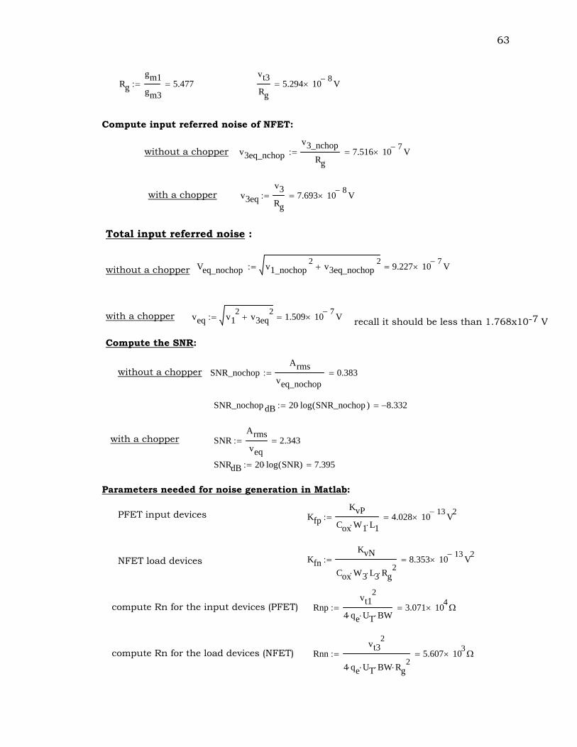
63
Rggm1gm3
5.477=:= vt3Rg
5.294 10 8−× V=
with a chopper v3eqv3Rg
7.693 10 8−× V=:=
Total input referred noise :
without a chopper
with a chopper veq v12 v3eq
2+ 1.509 10 7−
× V=:= recall it should be less than 1.768x10⁻⁷ V
Compute input referred noise of NFET:
v3eq_nchopv3_nchop
Rg7.516 10 7−
× V=:= without a chopper
Veq_nochop v1_nochop2 v3eq_nochop
2+ 9.227 10 7−
× V=:=
Compute the SNR:
without a chopper SNR_nochopArms
veq_nochop0.383=:=
SNR_nochop dB 20 log SNR_nochop( )⋅ 8.332−=:=
with a chopper SNRArmsveq
2.343=:=
SNRdB 20 log SNR( )⋅ 7.395=:=
Parameters needed for noise generation in Matlab:
PFET input devices KfpKvP
Cox W1⋅ L1⋅4.028 10 13−
× V2=:=
NFET load devices KfnKvN
Cox W3⋅ L3⋅ Rg2
⋅8.353 10 13−
× V2=:=
compute Rn for the input devices (PFET) Rnpvt1
2
4 qe⋅ UT⋅ BW⋅3.071 104
× Ω=:=
compute Rn for the load devices (NFET) Rnnvt3
2
4 qe⋅ UT⋅ BW⋅ Rg2
⋅5.607 103
× Ω=:=
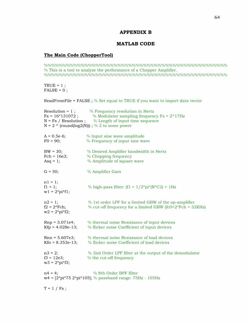
64
APPENDIX B
MATLAB CODE
The Main Code (ChopperTool)
%%%%%%%%%%%%%%%%%%%%%%%%%%%%%%%%%%%%%%%%%%%%%%%%%% % This is a tool to analyze the performance of a Chopper Amplifier. %%%%%%%%%%%%%%%%%%%%%%%%%%%%%%%%%%%%%%%%%%%%%%%%%% TRUE = 1 ; FALSE = 0 ; ReadFromFile = FALSE ; % Set equal to TRUE if you want to import data vector Resolution = 1 ; % Frequency resolution in Hertz Fs = 16*131072 ; % Modulator sampling frequency Fs = 2^17Hz N = Fs / Resolution ; % Length of input time sequence N = 2 ^ (round(log2(N))) ; % 2 to some power A = 0.5e-6; % Input sine wave amplitude F0 = 90; % Frequency of input sine wave BW = 30; % Desired Amplifier bandwidth in Hertz Fch = 16e3; % Chopping frequency Asq = 1; % Amplitude of square wave G = 50; % Amplifier Gain n1 = 1; f1 = 1; % high-pass filter: (f1 = 1/2*pi*(R*C2) = 1Hz w1 = 2*pi*f1; n2 = 1; % 1st order LPF for a limited GBW of the op-amplifier f2 = 2*Fch; % cut-off frequency for a limited GBW (fc0=2*Fch = 32KHz) w2 = 2*pi*f2; Rnp = 3.071e4; % thermal noise Resistance of input devices Kfp = 4.028e-13; % flicker noise Coefficient of input devices Rnn = 5.607e3; % thermal noise Resistance of load devices Kfn = 8.353e-13; % flicker noise Coefficient of load devices n3 = 2; % 2nd Order LPF filter at the output of the demodulator f3 = 12e3; % the cut-off frequency w3 = 2*pi*f3; n4 = 4; % 8th Order BPF filter w4 = [2*pi*75 2*pi*105]; % passband range: 75Hz - 105Hz T = 1 / Fs ;
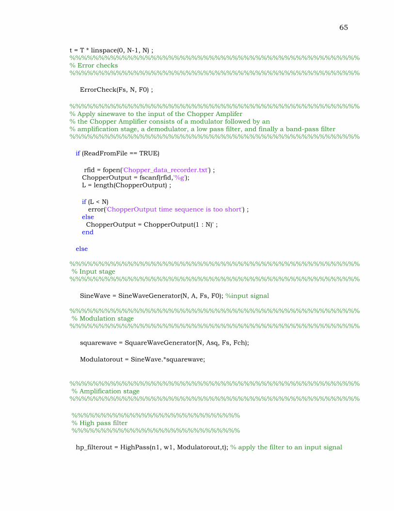
65
t = T * linspace(0, N-1, N) ; %%%%%%%%%%%%%%%%%%%%%%%%%%%%%%%%%%%%%%%%%%%%%%%%%% % Error checks %%%%%%%%%%%%%%%%%%%%%%%%%%%%%%%%%%%%%%%%%%%%%%%%%% ErrorCheck(Fs, N, F0) ; %%%%%%%%%%%%%%%%%%%%%%%%%%%%%%%%%%%%%%%%%%%%%%%%%% % Apply sinewave to the input of the Chopper Amplifer % the Chopper Amplifier consists of a modulator followed by an % amplification stage, a demodulator, a low pass filter, and finally a band-pass filter %%%%%%%%%%%%%%%%%%%%%%%%%%%%%%%%%%%%%%%%%%%%%%%%%% if (ReadFromFile == TRUE) rfid = fopen('Chopper_data_recorder.txt') ; ChopperOutput = fscanf(rfid,'%g'); L = length(ChopperOutput) ; if (L < N) error('ChopperOutput time sequence is too short') ; else ChopperOutput = ChopperOutput(1 : N)' ; end else %%%%%%%%%%%%%%%%%%%%%%%%%%%%%%%%%%%%%%%%%%%%%%%%%% % Input stage %%%%%%%%%%%%%%%%%%%%%%%%%%%%%%%%%%%%%%%%%%%%%%%%%% SineWave = SineWaveGenerator(N, A, Fs, F0); %input signal %%%%%%%%%%%%%%%%%%%%%%%%%%%%%%%%%%%%%%%%%%%%%%%%%% % Modulation stage %%%%%%%%%%%%%%%%%%%%%%%%%%%%%%%%%%%%%%%%%%%%%%%%%% squarewave = SquareWaveGenerator(N, Asq, Fs, Fch); Modulatorout = SineWave.*squarewave; %%%%%%%%%%%%%%%%%%%%%%%%%%%%%%%%%%%%%%%%%%%%%%%%%% % Amplification stage %%%%%%%%%%%%%%%%%%%%%%%%%%%%%%%%%%%%%%%%%%%%%%%%%% %%%%%%%%%%%%%%%%%%%%%%%%%%%%% % High pass filter %%%%%%%%%%%%%%%%%%%%%%%%%%%%% hp_filterout = HighPass(n1, w1, Modulatorout,t); % apply the filter to an input signal
66
%%%%%%%%%%%%%%%%%%%%%%%%%%% % Adding noise at the input %%%%%%%%%%%%%%%%%%%%%%%%%%% p_noise = NoiseGenerator(Rnp, Kfp, Fs, N); % Noise generation for input devices n_noise = NoiseGenerator(Rnn, Kfn, Fs, N); % Noise generation for load devices noise = p_noise + n_noise; % total noise Amplinput = hp_filterout + transpose(noise); % noise added at the input of the amplifier %%%%%%%%%%%%%%%%%%%%%%%%%%%% % Pure amplification %%%%%%%%%%%%%%%%%%%%%%%%%%%% Amp = G*Amplinput; %%%%%%%%%%%%%%%%%%%%%%%%%%%% % low-pass filter %%%%%%%%%%%%%%%%%%%%%%%%%%%% Ampliout = LowPass(n2, w2,Amp,t); % apply the low-pass filter to an input signal %%%%%%%%%%%%%%%%%%%%%%%%%%%%%%%%%%%%%%%%%%%%%%%%%% % Demodulation stage %%%%%%%%%%%%%%%%%%%%%%%%%%%%%%%%%%%%%%%%%%%%%%%%%% squarewave = SquareWaveGenerator(N, Asq, Fs, Fch); Demodulatorout = Ampliout.*transpose(squarewave); %%%%%%%%%%%%%%%%%%%%%%%%%%%%%%%%%%%%%%%%%%%%%%%%%% % Ouptut of the Chopper Amplifier %%%%%%%%%%%%%%%%%%%%%%%%%%%%%%%%%%%%%%%%%%%%%%%%%% ChopperOutput = Demodulatorout; %%%%%%%%%%%%%%%%%%%%%%%%%%%%%%%%%%%%%%%%%%%%%%%%%% % the filtring stage (2nd order LPF) %%%%%%%%%%%%%%%%%%%%%%%%%%%%%%%%%%%%%%%%%%%%%%%%%% Filterout = AAF(n3, w3, ChopperOutput, t); % apply the filter to an input signal end %%%%%%%%%%%%%%%%%%%%%%%%%%%%%%%%%%%%%%%%%%%%%%%%%% % Signal filtring stage (8th order BPF) %%%%%%%%%%%%%%%%%%%%%%%%%%%%%%%%%%%%%%%%%%%%%%%%%% BP_Filterout = BandPass(n4,w4,Filterout,t); % apply the filter to an input signal
67
%%%%%%%%%%%%%%%%%%%%%%%%%%%%%%%%%%%%%%%%%%%%%%%%%% % Lets use the middle group of samples in each array so that we don't have transients to contend with. %%%%%%%%%%%%%%%%%%%%%%%%%%%%%%%%%%%%%%%%%%%%%%%%%% % L = length(ChopperOutput) ; % ChopperOutput = ChopperOutput(L/4+1 : 5*L/4) ; % L = length(Filterout) ; % Filterout = Filterout(L/4+1 : 3*L/4) ; % L = length(DSP_Filterout) ; % DSP_Filterout = DSP_Filterout(L/4+1 : 3*L/4) ; %%%%%%%%%%%%%%%%%%%%%%%%%%%%%%%%%%%%%%%%%%%%%%%%%% % Take FFTs of the output waveforms %%%%%%%%%%%%%%%%%%%%%%%%%%%%%%%%%%%%%%%%%%%%%%%%%% ChopperOutputFFT = FFTmagnitude(transpose(ChopperOutput)); FilteroutFFT = FFTmagnitude(transpose(Filterout)); BP_FilteroutFFT = FFTmagnitude(transpose(BP_Filterout)); %%%%%%%%%%%%%%%%%%%%%%%%%%%%%%%%%%%%%%%%%%%%%%%%%% % Calculate the SNR %%%%%%%%%%%%%%%%%%%%%%%%%%%%%%%%%%%%%%%%%%%%%%%%%% ChopperOutputSNR = ComputeSNR(ChopperOutputFFT, Fs, F0, BW) FilteroutSNR = ComputeSNR(FilteroutFFT, Fs, F0, BW) BP_FilteroutSNR = ComputeSNR(BP_FilteroutFFT, Fs, F0, BW) %%%%%%%%%%%%%%%%%%%%%%%%%%%%%%%%%%%%%%%%%%%%%%%%%% % Plot in time domain so we can see of waveform looks reasonable %%%%%%%%%%%%%%%%%%%%%%%%%%%%%%%%%%%%%%%%%%%%%%%%%% figure(1) ; hold on ; TimeDomainPlot(SineWave, 1, Fs, 'b', 1, 4) ; TimeDomainPlot(ChopperOutput, 1, Fs, 'g', 2, 4) ; TimeDomainPlot(Filterout, 1, Fs, 'r', 3, 4) ; TimeDomainPlot(BP_Filterout, 1, Fs, 'b', 4, 4) ; hold off ; %%%%%%%%%%%%%%%%%%%%%%%%%%%%%%%%%%%%%%%%%%%%%%%%%% % Plot in the frequency domain %%%%%%%%%%%%%%%%%%%%%%%%%%%%%%%%%%%%%%%%%%%%%%%%%% figure(2) ; hold on ; FreqDomainPlot(ChopperOutputFFT, 1, Fs, 'b', 1, 3) ; FreqDomainPlot(FilteroutFFT, 1, Fs, 'g', 2, 3) ; FreqDomainPlot(BP_FilteroutFFT, 1, Fs, 'g', 3, 3) ; hold off ; %%%%%%%%%%%%%%%%%%%%%%%%%%%%%%%%%%%%%%%%%%%%%%%%%% %%%%%%%%%%%%%%%%%%%%%%%%%%%%%%%%%%%%%%%%%%%%%%%%%%
68
Sine-wave Generation function
function[SineWave] = SineWaveGenerator(N, A1, Fs, Fo) % % Generates a sinusoidal time sequency % % N is the number of samples to in the time sequence % A1 is the peak amplitude of the sine wave % Fs is the sampling frequency % Fo is the frequency of the sine wave in Hertz % % Fhat is the normalized frequency i.e. F0/Fs % %Resolution = 1 ; % Frequency resolution in Hertz %Fs = 131072 ; % Modulator sampling frequency Fs = 2^17Hz %N = Fs / Resolution ; % Length of input time sequence (2 to some power) %N = 2 ^ (round(log2(N))) ; %A1 = 1e-6; % Input sine wave amplitude %Fo = 90; % Frequency of input sine wave Fhat = Fo / Fs ; K = 2 * pi * Fhat ; index = linspace(0, N-1, N) ; SineWave = A1 * sin(K * index); %Ts = 1 / Fs ; %time = Ts * index ; %plot(time, SineWave) % end
69
Square-wave Generation function
function[SquareWave] = SquareWaveGenerator(N, A2, Fs, Fch) % % Generates a square wave sequency % % N is the number of samples to in the time sequence % A2 is the peak amplitude of the square wave % Fs is the sampling frequency % Fch is the frequency of the square wave in Hertz (chopper frequency) % %Resolution = 1 ; % Frequency resolution in Hertz %Fs = 131072 ; % Modulator sampling frequency Fs = 2^17Hz %N = Fs / Resolution ; % Length of input time sequence (2 to some power) %N = 2 ^ (round(log2(N))) ; %Fch=16e3; %A2=1; % % Fhat is the normalized frequency i.e. Fch/Fs % Fhat = Fch / Fs ; K = 2 * pi * Fhat ; index = linspace(0, N-1, N) ; SquareWave = A2 * square(K * index); %Ts = 1 / Fs ; %time = Ts * index ; %plot(time, SquareWave); % end
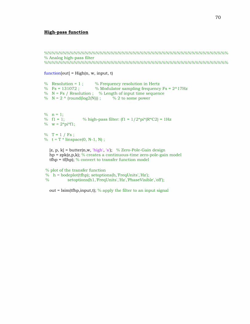
70
High-pass function
%%%%%%%%%%%%%%%%%%%%%%%%%%%%%%%%%%%%%%%%%%%%%%%%%% % Analog high-pass filter %%%%%%%%%%%%%%%%%%%%%%%%%%%%%%%%%%%%%%%%%%%%%%%%%% function[out] = High(n, w, input, t) % Resolution = 1 ; % Frequency resolution in Hertz % Fs = 131072 ; % Modulator sampling frequency Fs = 2^17Hz % N = Fs / Resolution ; % Length of input time sequence % N = 2 ^ (round(log2(N))) ; % 2 to some power % n = 1; % f1 = 1; % high-pass filter: (f1 = 1/2*pi*(R*C2) = 1Hz % w = 2*pi*f1; % T = 1 / Fs ; % t = T * linspace(0, N-1, N) ; [z, p, k] = butter(n,w, 'high', 's'); % Zero-Pole-Gain design hp = zpk(z,p,k); % creates a continuous-time zero-pole-gain model tfhp = tf(hp); % convert to transfer function model % plot of the transfer function % h = bodeplot(tfhp); setoptions(h,'FreqUnits','Hz'); % setoptions(h1,'FreqUnits','Hz','PhaseVisible','off'); out = lsim(tfhp,input,t); % apply the filter to an input signal
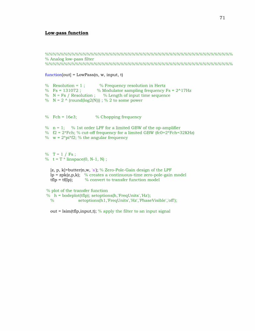
71
Low-pass function
%%%%%%%%%%%%%%%%%%%%%%%%%%%%%%%%%%%%%%%%%%%%%%%%%% % Analog low-pass filter %%%%%%%%%%%%%%%%%%%%%%%%%%%%%%%%%%%%%%%%%%%%%%%%%% function[out] = LowPass(n, w, input, t) % Resolution = 1 ; % Frequency resolution in Hertz % Fs = 131072 ; % Modulator sampling frequency Fs = 2^17Hz % N = Fs / Resolution ; % Length of input time sequence % N = 2 ^ (round(log2(N))) ; % 2 to some power % Fch = 16e3; % Chopping frequency % n = 1; % 1st order LPF for a limited GBW of the op-amplifier % f2 = 2*Fch; % cut-off frequency for a limited GBW (fc0=2*Fch=32KHz) % w = 2*pi*f2; % the angular frequency % T = 1 / Fs ; % t = T * linspace(0, N-1, N) ; [z, p, k]=butter(n,w, 's'); % Zero-Pole-Gain design of the LPF lp = zpk(z,p,k); % creates a continuous-time zero-pole-gain model tflp = tf(lp); % convert to transfer function model % plot of the transfer function % h = bodeplot(tflp); setoptions(h,'FreqUnits','Hz'); % setoptions(h1,'FreqUnits','Hz','PhaseVisible','off'); out = lsim(tflp,input,t); % apply the filter to an input signal
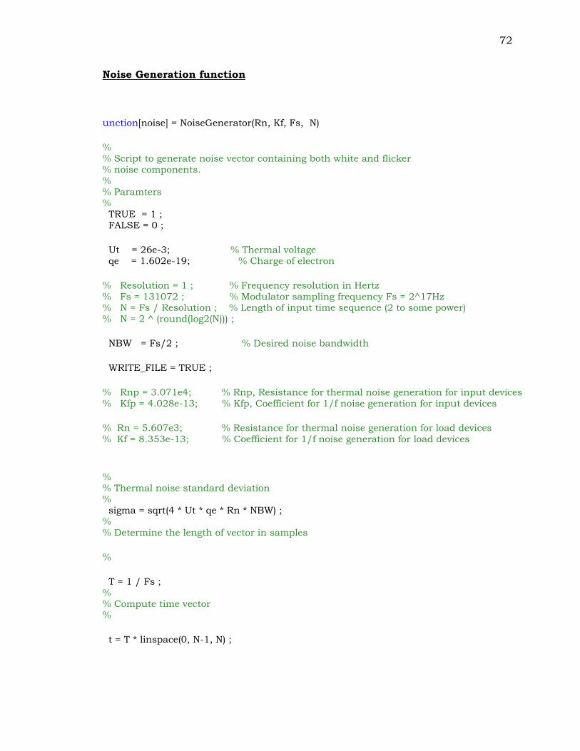
72
Noise Generation function
unction[noise] = NoiseGenerator(Rn, Kf, Fs, N) % % Script to generate noise vector containing both white and flicker % noise components. % % Paramters % TRUE = 1 ; FALSE = 0 ; Ut = 26e-3; % Thermal voltage qe = 1.602e-19; % Charge of electron % Resolution = 1 ; % Frequency resolution in Hertz % Fs = 131072 ; % Modulator sampling frequency Fs = 2^17Hz % N = Fs / Resolution ; % Length of input time sequence (2 to some power) % N = 2 ^ (round(log2(N))) ; NBW = Fs/2 ; % Desired noise bandwidth WRITE_FILE = TRUE ; % Rnp = 3.071e4; % Rnp, Resistance for thermal noise generation for input devices % Kfp = 4.028e-13; % Kfp, Coefficient for 1/f noise generation for input devices % Rn = 5.607e3; % Resistance for thermal noise generation for load devices % Kf = 8.353e-13; % Coefficient for 1/f noise generation for load devices % % Thermal noise standard deviation % sigma = sqrt(4 * Ut * qe * Rn * NBW) ; % % Determine the length of vector in samples % T = 1 / Fs ; % % Compute time vector % t = T * linspace(0, N-1, N) ;
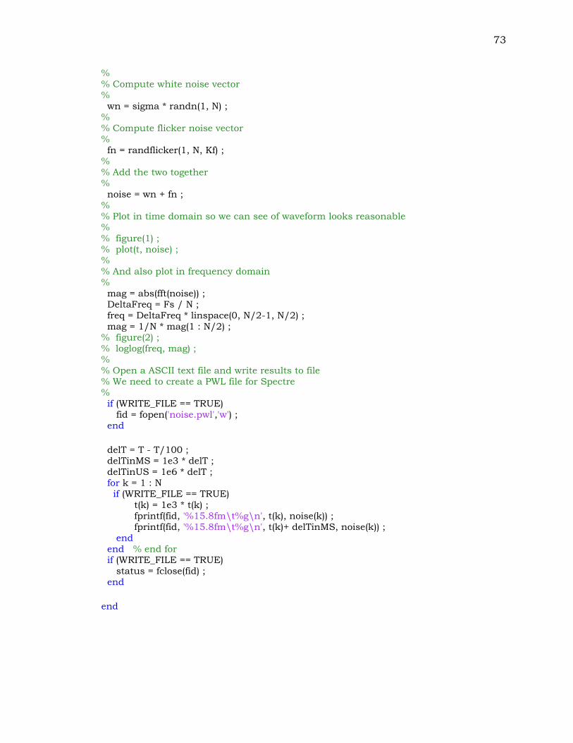
73
% % Compute white noise vector % wn = sigma * randn(1, N) ; % % Compute flicker noise vector % fn = randflicker(1, N, Kf) ; % % Add the two together % noise = wn + fn ; % % Plot in time domain so we can see of waveform looks reasonable % % figure(1) ; % plot(t, noise) ; % % And also plot in frequency domain % mag = abs(fft(noise)) ; DeltaFreq = Fs / N ; freq = DeltaFreq * linspace(0, N/2-1, N/2) ; mag = 1/N * mag(1 : N/2) ; % figure(2) ; % loglog(freq, mag) ; % % Open a ASCII text file and write results to file % We need to create a PWL file for Spectre % if (WRITE_FILE == TRUE) fid = fopen('noise.pwl','w') ; end delT = T - T/100 ; delTinMS = 1e3 * delT ; delTinUS = 1e6 * delT ; for k = 1 : N if (WRITE_FILE == TRUE) t(k) = 1e3 * t(k) ; fprintf(fid, '%15.8fm\t%g\n', t(k), noise(k)) ; fprintf(fid, '%15.8fm\t%g\n', t(k)+ delTinMS, noise(k)) ; end end % end for if (WRITE_FILE == TRUE) status = fclose(fid) ; end end
74
Anti-Aliasing Filter function
%%%%%%%%%%%%%%%%%%%%%%%%%%%%%%%%%%%%%%%%%%%%%%%%%% % Anti-Aliasing Filter (2nd order Analog low-pass filter) %%%%%%%%%%%%%%%%%%%%%%%%%%%%%%%%%%%%%%%%%%%%%%%%%% function[out] = AAF(n, w, input, t) % Resolution = 1 ; % Frequency resolution in Hertz % Fs = 131072 ; % Modulator sampling frequency Fs = 2^17Hz % N = Fs / Resolution ; % Length of input time sequence (2 to some power) % N = 2 ^ (round(log2(N))) ; % n = 2; % 2st order LPF for a limited GBW of the op-amplifier % f3 = 12e3; % cut-off frequency for a limited GBW (fc0 = 2*Fch = 32 KHz) % w = 2*pi*f3; % the angular frequency % T = 1 / Fs ; % t = T * linspace(0, N-1, N) ; [z, p, k]=butter(n,w, 's'); % Zero-Pole-Gain design lp = zpk(z,p,k); % creates a continuous-time zero-pole-gain model tflp = tf(lp); % convert to transfer function model % plot of the transfer function % h = bodeplot(tflp); setoptions(h,'FreqUnits','Hz'); % setoptions(h1,'FreqUnits','Hz','PhaseVisible','off'); out = lsim(tflp,input,t); % apply the filter to an input signal
75
Band-Pass Filter function
%%%%%%%%%%%%%%%%%%%%%%%%%%%%%%%%%%%%%%%%%%%%%%%%%% % 8th order DSP Band-Pass filter %%%%%%%%%%%%%%%%%%%%%%%%%%%%%%%%%%%%%%%%%%%%%%%%%% function[out] = BandPass(n, w, input, t) % Resolution = 1 ; % Frequency resolution in Hertz % Fs = 131072 ; % Modulator sampling frequency Fs = 2^17Hz % N = Fs / Resolution ; % Length of input time sequence (2 to some power) % N = 2 ^ (round(log2(N))) ; % n = 4; % 8th Order BPF filter % w = [2*pi*75 2*pi*105]; % passband range: 75Hz - 105Hz % T = 1 / Fs ; % t = T * linspace(0, N-1, N) ; [z, p, k]=butter(n,w,'s'); % zero-pole-gain design bp = zpk(z,p,k); % creates a continuous-time zero-pole-gain model tfbp = tf(bp), % convert to transfer function model % plot of the transfer function % h = bodeplot(tfbp); setoptions(h,'FreqUnits','Hz'); out = lsim(tfbp,input,t); % apply the filter to an input signal
76
FFT Magnitude Computation function
function[out] = FFTmagnitude(Waveform) % % Using Hodie window to minimize spectral blurring % L = length(Waveform) ; coefficients = HodieWindow(L) ; WindowedWaveform = Waveform .* coefficients' ; % % Return magnitude part of FFT % out = abs(fft(WindowedWaveform)) ; end
Hodie Window function
function [out] = HodieWindow(N) % % Script to compute a N-term floating point Hodie window % Copyright 2001 Eric Swanson % N is the number of filter coefficients % window = zeros(N,1); bottom = zeros(N,1); top = 2.5 * ones(N,1); index = [0:N-1]'; v = 2 * pi / N; % % Hodie window cosine coefficients % a0=0.61640321314050; a1=0.98537119272586; a2=0.49603771622007; a3=0.14992232793243; a4=0.02458719103474; a5=0.00176604651487; a6=0.00003158118857; % % Coefficients sum to N % for m=1:N; n1=m-.5; window(m,1)=a0-a1*cos(v*n1)+a2*cos(v*2*n1)-a3*cos(v*3*n1)+a4*cos(v*4*n1)-a5*cos(v*5*n1)+a6*cos(v*6*n1); end; out = window; % %plot % %plot(index,window,'-g',index,bottom,'-b',index,top,'-b'); %axis([0 1000 0 2.5]); %axis off;
77
SNR Computation function
function [SNR] = ComputeSNR(FFT, Fs, Fo, BW) % % Script to compute signal-noise-ratio % % % Compute signal bin % L = length(FFT) ; BinSize = Fs / L ; SignalBin= round(Fo/BinSize) ; % % Hodie Window confines spectrum to Signal Bin +/- 8 bins % LowerSignalBin = SignalBin - 8 ; UpperSignalBin = SignalBin + 8 ; % % Compute end of BW bin % BWbin= round(BW/BinSize) ; SumSignalSquared = 0.0 ; SumNoiseSquared = 0.0 ; % % Calculate noise power preceding signal bins % for k = 2 : 1: (LowerSignalBin - 1) SumNoiseSquared = SumNoiseSquared + FFT(k) * FFT(k); end % % Estimate the noise power in the signal bins % EstNoisePwr = FFT(LowerSignalBin - 1) * FFT(LowerSignalBin - 1) ; EstNoisePwr = EstNoisePwr + FFT(UpperSignalBin + 1) * FFT(UpperSignalBin + 1) ; EstNoisePwr = EstNoisePwr / 2.0 ; % % Calculate signal power % for k = LowerSignalBin: 1 : UpperSignalBin SumSignalSquared = SumSignalSquared + FFT(k) * FFT(k) - EstNoisePwr ; SumNoiseSquared = SumNoiseSquared + EstNoisePwr ; end % % Calculate noise power after signal bins % for k = UpperSignalBin + 1 : 1 : BWbin SumNoiseSquared = SumNoiseSquared + FFT(k) * FFT(k) ; end SNR = 10 * log10(SumSignalSquared/SumNoiseSquared); end
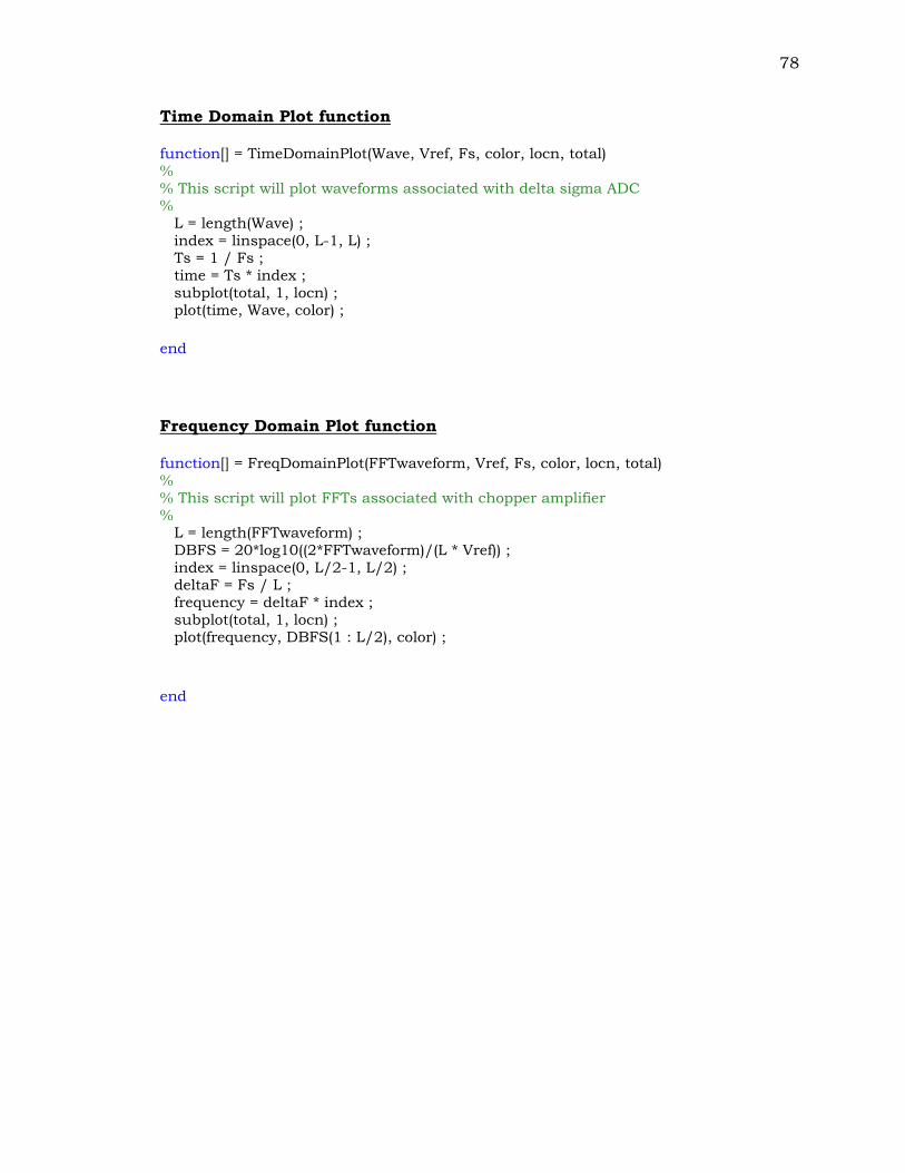
78
Time Domain Plot function
function[] = TimeDomainPlot(Wave, Vref, Fs, color, locn, total) % % This script will plot waveforms associated with delta sigma ADC % L = length(Wave) ; index = linspace(0, L-1, L) ; Ts = 1 / Fs ; time = Ts * index ; subplot(total, 1, locn) ; plot(time, Wave, color) ; end
Frequency Domain Plot function
function[] = FreqDomainPlot(FFTwaveform, Vref, Fs, color, locn, total) % % This script will plot FFTs associated with chopper amplifier % L = length(FFTwaveform) ; DBFS = 20*log10((2*FFTwaveform)/(L * Vref)) ; index = linspace(0, L/2-1, L/2) ; deltaF = Fs / L ; frequency = deltaF * index ; subplot(total, 1, locn) ; plot(frequency, DBFS(1 : L/2), color) ; end
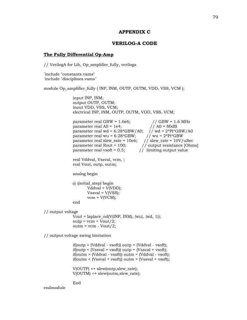
79
APPENDIX C
VERILOG-A CODE
The Fully Differential Op-Amp
// VerilogA for Lib, Op_amplifier_fully, veriloga `include "constants.vams" `include "disciplines.vams" module Op_amplifier_fully ( INP, INM, OUTP, OUTM, VDD, VSS, VCM ); input INP, INM; output OUTP, OUTM; inout VDD, VSS, VCM; electrical INP, INM, OUTP, OUTM, VDD, VSS, VCM; parameter real GBW = 1.6e6; // GBW = 1.6 MHz parameter real A0 = 1e4; // A0 = 80dB parameter real wd = 6.28*GBW/A0; // wd = 2*Pi*GBW/A0 parameter real wu = 6.28*GBW; // wu = 2*Pi*GBW parameter real slew_rate = 10e6; // slew_rate = 10V/uSec parameter real Rout = 100; // output resistance [Ohms] parameter real vsoft = 0.5; // limiting output value real Vddval, Vssval, vcm, ; real Vout, outp, outm; analog begin @ (initial_step) begin Vddval = V(VDD); Vssval = V(VSS); vcm = V(VCM); end // output voltage Vout = laplace_nd(V(INP, INM), wu, wd, 1); outp = vcm + Vout/2; outm = vcm - Vout/2; // output voltage swing limitation if(outp > (Vddval - vsoft)) outp = (Vddval - vsoft); if(outp < (Vssval + vsoft)) outp = (Vssval + vsoft); if(outm > (Vddval - vsoft)) outm = (Vddval - vsoft); if(outm < (Vssval + vsoft)) outm = (Vssval + vsoft); V(OUTP) <+ slew(outp,slew_rate); V(OUTM) <+ slew(outm,slew_rate); End endmodule
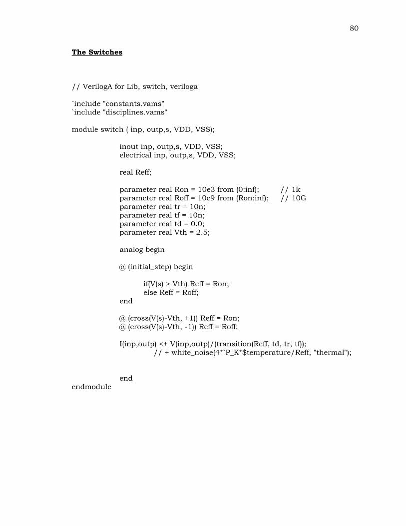
80
The Switches
// VerilogA for Lib, switch, veriloga `include "constants.vams" `include "disciplines.vams" module switch ( inp, outp,s, VDD, VSS); inout inp, outp,s, VDD, VSS; electrical inp, outp,s, VDD, VSS; real Reff; parameter real Ron = 10e3 from (0:inf); // 1k parameter real Roff = 10e9 from (Ron:inf); // 10G parameter real tr = 10n; parameter real tf = 10n; parameter real td = 0.0; parameter real Vth = 2.5; analog begin @ (initial_step) begin if(V(s) > Vth) Reff = Ron; else Reff = Roff; end @ (cross(V(s)-Vth, +1)) Reff = Ron; @ (cross(V(s)-Vth, -1)) Reff = Roff;
I(inp,outp) <+ V(inp,outp)/(transition(Reff, td, tr, tf)); // + white_noise(4*`P_K*$temperature/Reff, "thermal"); end endmodule
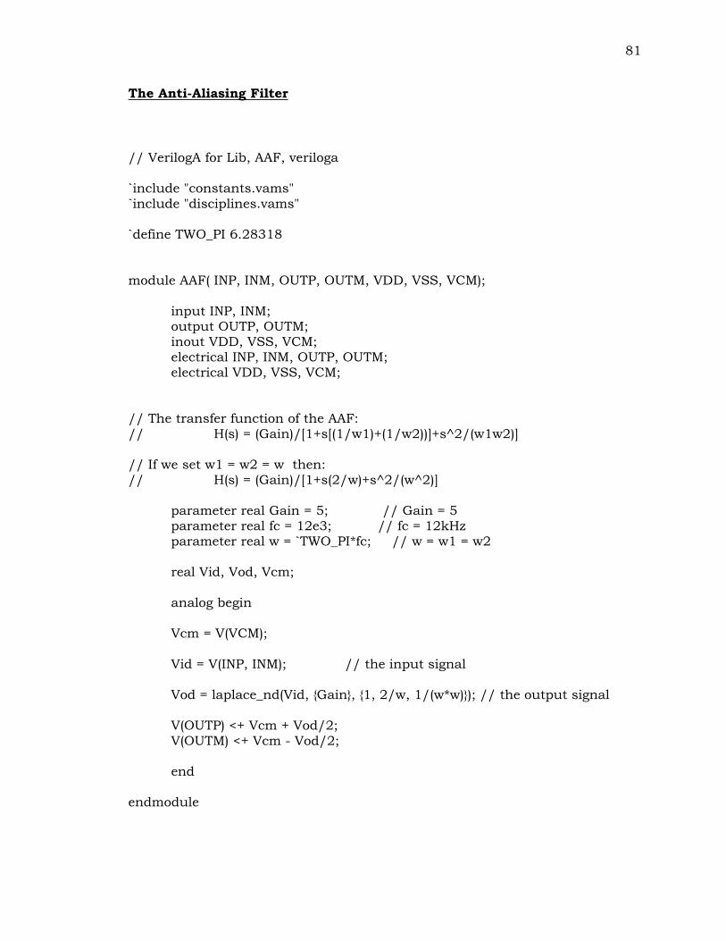
81
The Anti-Aliasing Filter
// VerilogA for Lib, AAF, veriloga `include "constants.vams" `include "disciplines.vams" `define TWO_PI 6.28318 module AAF( INP, INM, OUTP, OUTM, VDD, VSS, VCM); input INP, INM; output OUTP, OUTM; inout VDD, VSS, VCM; electrical INP, INM, OUTP, OUTM; electrical VDD, VSS, VCM; // The transfer function of the AAF: // H(s) = (Gain)/[1+s[(1/w1)+(1/w2))]+s^2/(w1w2)] // If we set w1 = w2 = w then: // H(s) = (Gain)/[1+s(2/w)+s^2/(w^2)] parameter real Gain = 5; // Gain = 5 parameter real fc = 12e3; // fc = 12kHz parameter real w = `TWO_PI*fc; // w = w1 = w2 real Vid, Vod, Vcm; analog begin Vcm = V(VCM); Vid = V(INP, INM); // the input signal Vod = laplace_nd(Vid, Gain, 1, 2/w, 1/(w*w)); // the output signal V(OUTP) <+ Vcm + Vod/2; V(OUTM) <+ Vcm - Vod/2; end endmodule
82
The Band-Pass Filter
// VerilogA for Lib, BPF_90Hz, veriloga `include "constants.vams" `include "disciplines.vams" `define TWO_PI 6.28318 module BPF_90Hz(INP, INM, OUTP, OUTM, VDD, VSS, VCM); input INP, INM; output OUTP, OUTM; inout VDD, VSS, VCM; electrical INP, INM, OUTP, OUTM; electrical VDD, VSS, VCM; real Vid, Vod, Vcm; analog begin Vcm = V(VCM); Vid = V(INP, INM); // the input signal // 8th order band-pass filter (75Hz – 105Hz) // the output signal
Vod = laplace_nd(Vid, 0,0,0,0,1.262e9, 9.342e21, 1.48e19, 1.319e17, 1.483e14, 6.566e11, 4.769e8, 1.365e6, 492.6, 1);
V(OUTP) <+ Vcm + Vod/2; V(OUTM) <+ Vcm - Vod/2; end endmodule
83
The Notch Filter
// VerilogA for Lib, Notch_60Hz, veriloga `include "constants.vams" `include "disciplines.vams" `define TWO_PI 6.28318 module Notch_60Hz(INP, INM, OUTP, OUTM, VDD, VSS, VCM); input INP, INM; output OUTP, OUTM; inout VDD, VSS, VCM; electrical INP, INM, OUTP, OUTM; electrical VDD, VSS, VCM; real Vid, Vod, Vcm; analog begin Vcm = V(VCM); Vid = V(INP, INM); // the input signal // 4th order rejection filter (Notch) of 60Hz signal
Vod = laplace_nd(Vid, 1.992e10,0,2.823e5,0,1, 1.992e10, 1.254e7, 2.862e5, 88.86, 1); // the output signal
V(OUTP) <+ Vcm + Vod/2; V(OUTM) <+ Vcm - Vod/2; end endmodule