Embed Size (px)
Citation preview
IDEC Journal of Integrated Circuits and Systems, VOL 02, No.1, April 2016 http://www.idec.or.kr
64
Abstract - This paper proposes design of a 10-bit Successive
Approximation Register (SAR) Analog to Digital Converter
(ADC) reducing device mismatching property driven by MSB
node of C-DAC array divided into 4 equal parts. It improves
linearity by adding switch for reducing mismatch of MSB node
which is the highest portion of mismatch in C-DAC array. The
proposed SAR ADC is fabricated in 180nm CMOS and
occupies a core area of 850um х 650um. It consumes 66.4uW
and achieves an ENOB of 9.3 bits at sampling frequency
800kS/s and power supply of 1.8V. The Figure of Merit (FOM)
is simulated to be 134.31fJ/step.
I. INTRODUCTION
With emphasizing welfare and convenience in this
contemporary society, it develops not only medical devices
which are portable or implantable medical devices but also a
variety of mobile devices. In accordance with this, it drives
research to design low power integrated circuit widely. SAR
ADCs consume only dynamic powers, which result in low
power and is suitable for low power application. Most of
SAR ADCs in the literature [1-3] suffered from poor
linearity problems. These poor linearity problems are
attributed to the poor linearity of C-DAC array within ADC.
Most of SAR ADCs employ a split capacitor to minimize
the magnitude of the unit capacitor. However, the size of the
MSB capacitor within C-DAC array still remains large,
which causes a linearity problem. This paper proposes a
technique to divide the size of MSB capacitor into four
equal sub capacitors, such that the matching property of C-
DAC is to be enhanced.
The paper is organized as follows. Section II introduces
the proposed architecture and describes the operational
principle of the proposed SAR ADC with simulation results.
Conclusions are drawn in Section III.
II. THE PROPOSED ARCHITECTURE
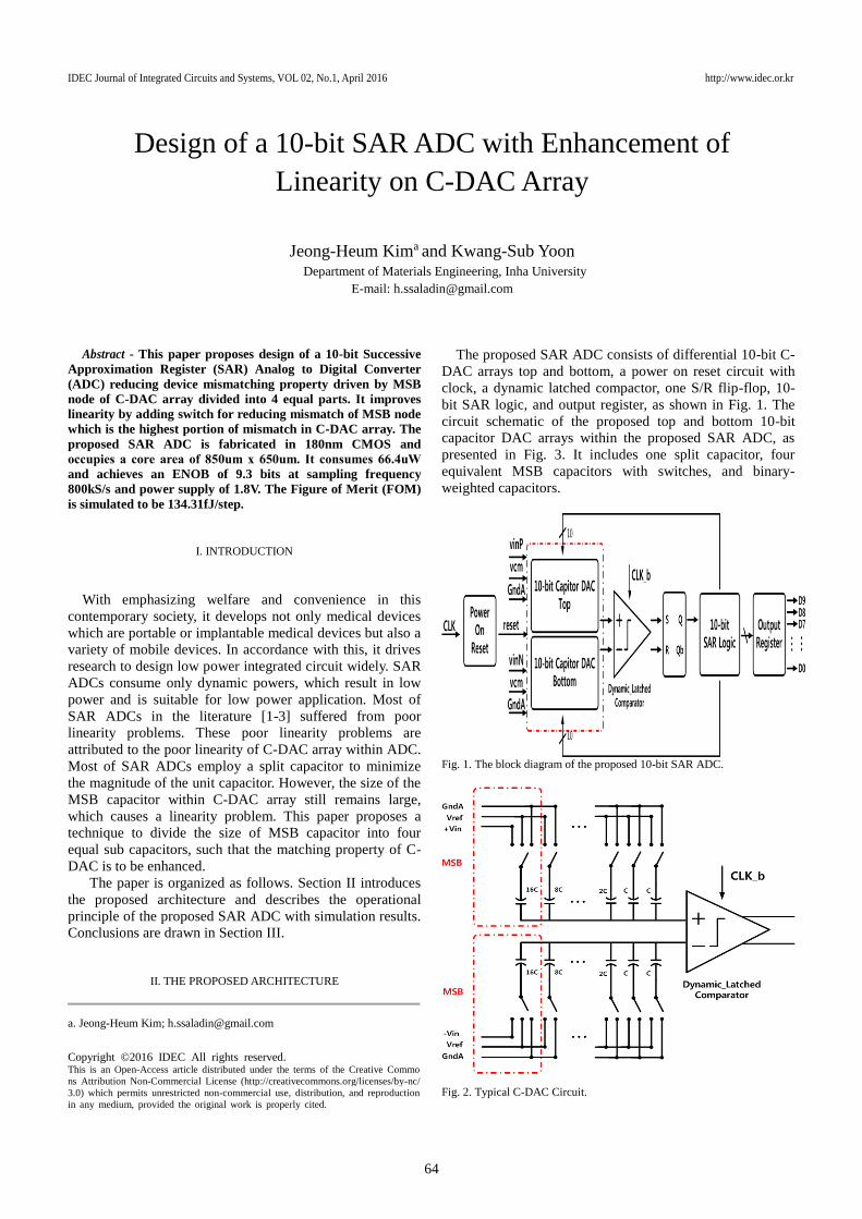
The proposed SAR ADC consists of differential 10-bit C-
DAC arrays top and bottom, a power on reset circuit with
clock, a dynamic latched compactor, one S/R flip-flop, 10-
bit SAR logic, and output register, as shown in Fig. 1. The
circuit schematic of the proposed top and bottom 10-bit
capacitor DAC arrays within the proposed SAR ADC, as
presented in Fig. 3. It includes one split capacitor, four
equivalent MSB capacitors with switches, and binary-
weighted capacitors.
Fig. 1. The block diagram of the proposed 10-bit SAR ADC.
Fig. 2. Typical C-DAC Circuit.
a. Jeong-Heum Kim; [email protected]
Copyright © 2016 IDEC All rights reserved. This is an Open-Access article distributed under the terms of the Creative Commo
ns Attribution Non-Commercial License (http://creativecommons.org/licenses/by-nc/
3.0) which permits unrestricted non-commercial use, distribution, and reproduction
in any medium, provided the original work is properly cited.
Design of a 10-bit SAR ADC with Enhancement of
Linearity on C-DAC Array
Jeong-Heum Kima and Kwang-Sub Yoon
Department of Materials Engineering, Inha University
E-mail: [email protected]
IDEC Journal of Integrated Circuits and Systems, VOL 02, No.1, April 2016 http://www.idec.or.kr
65
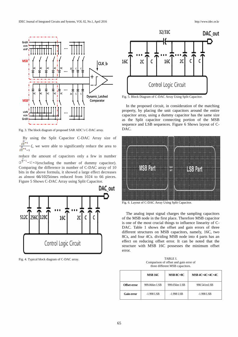
Fig. 3. The block diagram of proposed SAR ADC’s C-DAC array.
By using the Split Capacitor C-DAC Array size of
, we were able to significantly reduce the area to
reduce the amount of capacitors only a few in number
(excluding the number of dummy capacitor).
Comparing the difference in number of C-DAC array of 10
bits in the above formula, it showed a large effect decreases
as almost 66/1025times reduced from 1024 to 66 pieces.
Figure 5 Shows C-DAC Array using Split Capacitor.
Fig. 4. Typical block diagram of C-DAC array.
Fig. 5. Block Diagram of C-DAC Array Using Split Capacitor.
In the proposed circuit, in consideration of the matching
property, by placing the unit capacitors around the entire
capacitor array, using a dummy capacitor has the same size
as the Split capacitor connecting portion of the MSB
sequence and LSB sequences. Figure 6 Shows layout of C-
DAC.
Fig. 6. Layout of C-DAC Array Using Split Capacitor.
The analog input signal charges the sampling capacitors
of the MSB node in the first place. Therefore MSB capacitor
is one of the most crucial things to influence linearity of C-
DAC. Table 1 shows the offset and gain errors of three
different structures on MSB capacitors, namely, 16C, two
8Cs, and four 4Cs. dividing MSB node into 4 parts has an
effect on reducing offset error. It can be noted that the
structure with MSB 16C possesses the minimum offset
error.
TABLE I.
Comparison of offset and gain error of
three different MSB capacitors.
MSB 16C MSB 8C+8C MSB 4C+4C+4C+4C
Offset error 999.066m LSB 999.056m LSB 998.541mLSB
Gain error -1.998 LSB -1.998 LSB -1.998 LSB
IDEC Journal of Integrated Circuits and Systems, VOL 02, No.1, April 2016 http://www.idec.or.kr
66
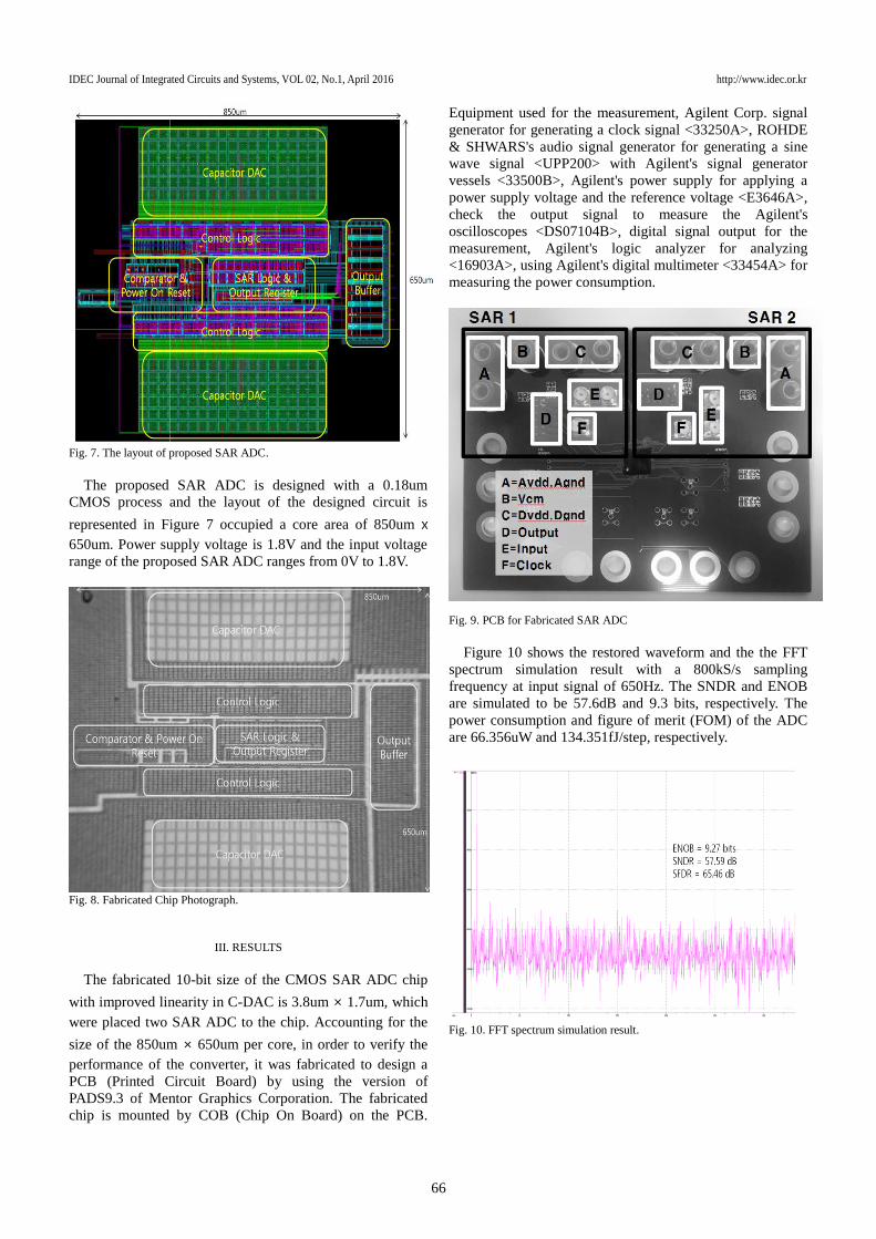
Fig. 7. The layout of proposed SAR ADC.
The proposed SAR ADC is designed with a 0.18um
CMOS process and the layout of the designed circuit is
represented in Figure 7 occupied a core area of 850um х
650um. Power supply voltage is 1.8V and the input voltage
range of the proposed SAR ADC ranges from 0V to 1.8V.
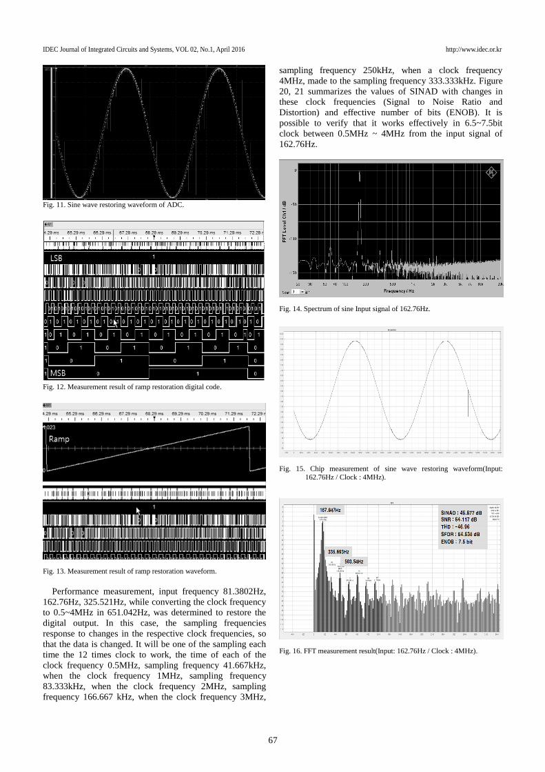
Fig. 8. Fabricated Chip Photograph.
III. RESULTS
The fabricated 10-bit size of the CMOS SAR ADC chip
with improved linearity in C-DAC is 3.8um × 1.7um, which
were placed two SAR ADC to the chip. Accounting for the
size of the 850um × 650um per core, in order to verify the
performance of the converter, it was fabricated to design a
PCB (Printed Circuit Board) by using the version of
PADS9.3 of Mentor Graphics Corporation. The fabricated
chip is mounted by COB (Chip On Board) on the PCB.
Equipment used for the measurement, Agilent Corp. signal
generator for generating a clock signal <33250A>, ROHDE
& SHWARS's audio signal generator for generating a sine
wave signal <UPP200> with Agilent's signal generator
vessels <33500B>, Agilent's power supply for applying a
power supply voltage and the reference voltage <E3646A>,
check the output signal to measure the Agilent's
oscilloscopes <DS07104B>, digital signal output for the
measurement, Agilent's logic analyzer for analyzing
<16903A>, using Agilent's digital multimeter <33454A> for
measuring the power consumption.
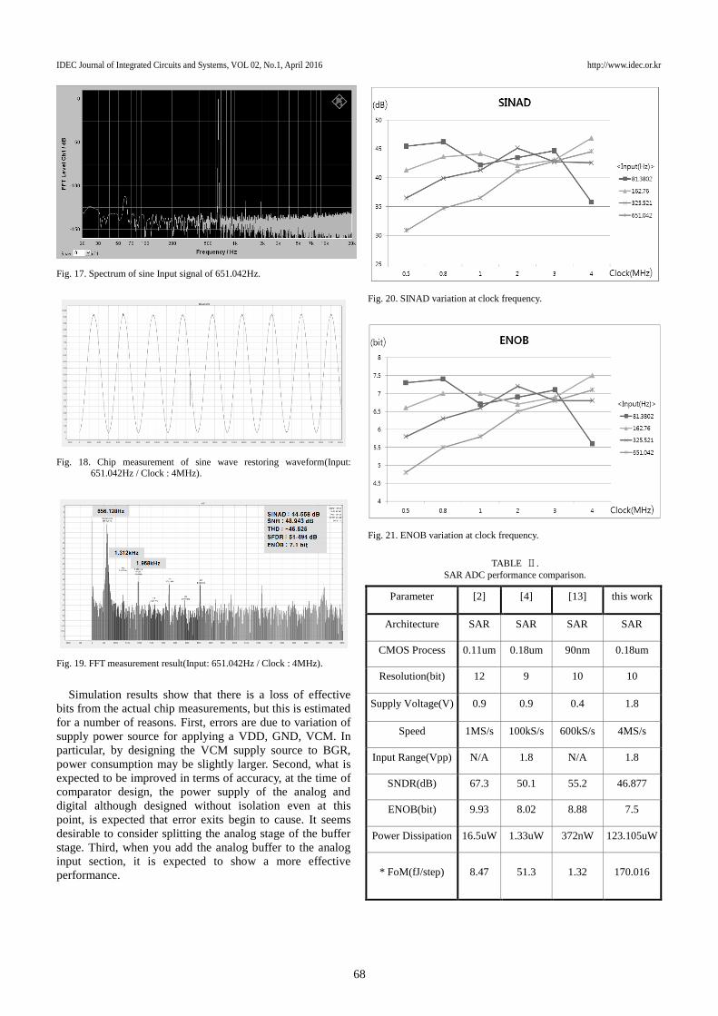
Fig. 9. PCB for Fabricated SAR ADC
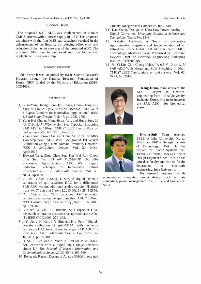
Figure 10 shows the restored waveform and the the FFT
spectrum simulation result with a 800kS/s sampling
frequency at input signal of 650Hz. The SNDR and ENOB
are simulated to be 57.6dB and 9.3 bits, respectively. The
power consumption and figure of merit (FOM) of the ADC
are 66.356uW and 134.351fJ/step, respectively.
Fig. 10. FFT spectrum simulation result.
IDEC Journal of Integrated Circuits and Systems, VOL 02, No.1, April 2016 http://www.idec.or.kr
67
Fig. 11. Sine wave restoring waveform of ADC.
Fig. 12. Measurement result of ramp restoration digital code.
Fig. 13. Measurement result of ramp restoration waveform.
Performance measurement, input frequency 81.3802Hz,
162.76Hz, 325.521Hz, while converting the clock frequency
to 0.5~4MHz in 651.042Hz, was determined to restore the
digital output. In this case, the sampling frequencies
response to changes in the respective clock frequencies, so
that the data is changed. It will be one of the sampling each
time the 12 times clock to work, the time of each of the
clock frequency 0.5MHz, sampling frequency 41.667kHz,
when the clock frequency 1MHz, sampling frequency
83.333kHz, when the clock frequency 2MHz, sampling
frequency 166.667 kHz, when the clock frequency 3MHz,
sampling frequency 250kHz, when a clock frequency
4MHz, made to the sampling frequency 333.333kHz. Figure
20, 21 summarizes the values of SINAD with changes in
these clock frequencies (Signal to Noise Ratio and
Distortion) and effective number of bits (ENOB). It is
possible to verify that it works effectively in 6.5~7.5bit
clock between 0.5MHz ~ 4MHz from the input signal of
162.76Hz.
Fig. 14. Spectrum of sine Input signal of 162.76Hz.
Fig. 15. Chip measurement of sine wave restoring waveform(Input:
162.76Hz / Clock : 4MHz).
Fig. 16. FFT measurement result(Input: 162.76Hz / Clock : 4MHz).
IDEC Journal of Integrated Circuits and Systems, VOL 02, No.1, April 2016 http://www.idec.or.kr
68
Fig. 17. Spectrum of sine Input signal of 651.042Hz.
Fig. 18. Chip measurement of sine wave restoring waveform(Input:
651.042Hz / Clock : 4MHz).
Fig. 19. FFT measurement result(Input: 651.042Hz / Clock : 4MHz).
Simulation results show that there is a loss of effective
bits from the actual chip measurements, but this is estimated
for a number of reasons. First, errors are due to variation of
supply power source for applying a VDD, GND, VCM. In
particular, by designing the VCM supply source to BGR,
power consumption may be slightly larger. Second, what is
expected to be improved in terms of accuracy, at the time of
comparator design, the power supply of the analog and
digital although designed without isolation even at this
point, is expected that error exits begin to cause. It seems
desirable to consider splitting the analog stage of the buffer
stage. Third, when you add the analog buffer to the analog
input section, it is expected to show a more effective
performance.
Fig. 20. SINAD variation at clock frequency.
Fig. 21. ENOB variation at clock frequency.
TABLE Ⅱ.
SAR ADC performance comparison.
Parameter [2] [4] [13] this work
Architecture SAR SAR SAR SAR
CMOS Process 0.11um 0.18um 90nm 0.18um
Resolution(bit) 12 9 10 10
Supply Voltage(V) 0.9 0.9 0.4 1.8
Speed 1MS/s 100kS/s 600kS/s 4MS/s
Input Range(Vpp) N/A 1.8 N/A 1.8
SNDR(dB) 67.3 50.1 55.2 46.877
ENOB(bit) 9.93 8.02 8.88 7.5
Power Dissipation 16.5uW 1.33uW 372nW 123.105uW
* FoM(fJ/step) 8.47 51.3 1.32 170.016
IDEC Journal of Integrated Circuits and Systems, VOL 02, No.1, April 2016 http://www.idec.or.kr
69
IV. CONCLUSIONS
The proposed SAR ADC was implemented in 0.18um
CMOS process with a power supply of 1.8V. The proposed
technique with the four MSB sub-capacitors resulted in the
enhancement of the linearity by reducing offset error and
reduction of the layout core area of the proposed ADC. The
proposed ADC can be employed into the biomedical/
implantable System on a chip.
ACKNOWLEDGMENT
This research was supported by Basic Science Research
Program through the National Research Foundation of
Korea (NRF) funded by the Ministry of Education (2010-
0020163).
REFERENCES
[1] Guan-Ying Huang, Soon-Jyh Chang, Chun-Cheng Liu,
Ying-Zu Lin “A 1-µW 10-bit 200-kS/s SAR ADC With
a Bypass Window for Biomedical Applications” IEEE
J. Solid-State Circuits, Vol. 47, pp. 2783-2795.
[2] Yung-Hui Chung, Meng-Hsuan Wu, and Hung-Sung Li
“A 12-bit 8.47-fJ/Conversion-Step Capacitor-Swapping
SAR ADC in 110-nm CMOS” IEEE Transactions on
and systems, Vol. 62, NO.1, Jan.2015.
[3] Yuan Zhou, Benwei Xu, Yun Chiu, “A 12 bit 160 MS/s
Two-Step SAR ADC With Background Bit-Weight
Calibration Using a Time-Domain Proximity Detector”
IEEE J. Solid-State Circuits, Vol. 50, NO.4,
April.2015.
[4] Howard Tang, Zhuo Chao Sun, Kin Wai Roy Chew,
Liter Siek “A 1.33 uW 8.02-ENOB 100 kS/s
Successive Approximation ADC With Supply
Reduction Technique for Implantable Retinal
Prosthesis” IEEE J. Solid-State Circuits, Vol. 50,
NO.4, April.2015.
[5] J. Um, Y.Kim, E.Song, J. Sim, A digital- domain
calibration of split-capacitor DAC for a differential
SAR ADC without additional analog circuits [J]. IEEE
trans. on Circuit and System I,2013 60(11), 2845-2856.
[6] Y. Chen et al., “Split capacitor DAC mismatch
calibration in successive approximation ADC,” in Proc.
IEEE Custom Integr. Circuits Conf., Sep. 13.16, 2009,
pp. 279.282.
[7] Y Chen, X. Zhu, T. Hirotaka. Split capacitor DAC
mismatch calibration in successive approximation ADC
[J]. IEEE CICC,2009, 279–282.
[8] J. Y. Um, J. H. Kim, J. Y. Sim, and H. J. Park, “Digital-
domain calibration of split-CDAC with no extra
calibration DAC for a differential- type SAR ADC,” in
Proc. IEEE Asian Solid-State Circuits Conf.,Nov. 14–
16, 2011, pp. 77–80.
[9] D. Shi, S. Lee, and K. Yoon. A 6-bit 500MS/s CMOS
A/D converter with a digital input range detection
circuit [J]. The Journal of Korean Information and
Communications Society,2013, 38(4), 303-309.
[10] Behazade Razavi, Design of Analog CMOS Integrated
Circuits, Macgaw-Hill Companies, Inc., 2001.
[11] Dai Zhang, Design of Ultra-Low-Power Analog-to-
Digital Converters, Linkoping Studies in Science and
Technology, Thesis No. 1548.
[12] Raheleh Hedayati, A Study of Successive
Approximation Registers and Implementation of an
Ultra-Low Power 10-bit SAR ADC in 65nm CMOS
Technology, Masters’s thesis Performed in Electronic
Devices, Dept. of Electrical Engineering Linkoping
Institue of Technology
[13] Jin-Yi Lin, Chih-Cheng Hsieh, “A 0.3 V 10-bit 1.17f
SAR ADC With Merge and Split Switching in 90nm
CMOS” IEEE Transactions on and systems, Vol. 62,
NO.1, Jan.2015.
Jeong-Heum Kim received the
M.S. degree in electrical
engineering from Inha University,
Incheon, Korea. His main interests
are SAR ADC for biomedical
system.
Kwang-Sub Yoon received
BSEE at Inha University, Korea,
MSEE and PhD at Georgia Institute
of Technology, USA. He has
worked for Silicon Systems Inc.,
Tustin, California, USA as a Senior
Design Engineer.Since 1992, he has
joined as faculty and worked for the
department of electronic
engineering, Inha University.
His research interests include
mixed-signal integrated circuit design such as data
converters, power management ICs, PLLs, and biomedical
SoCs.