Embed Size (px)
Citation preview

Design Methods and Circuit Techniques to Reduce Leakage in Deep Submicron
Christian Piguet, CSEM, Neuchâtel, Switzerland
Stefan Cserveny, CSEM
Jean-Félix Perotto, CSEM
Jean-Marc Masgonty, CSEM
C. Piguet :: 18.04.23 :: Page 3
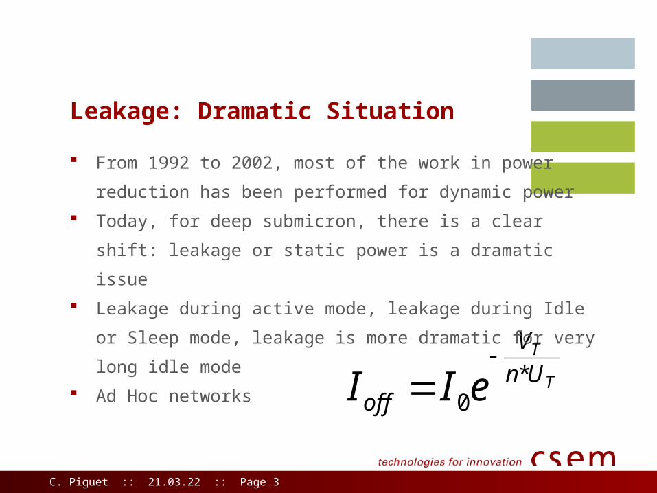
Leakage: Dramatic Situation
T
T
Un
V
off eII *0
From 1992 to 2002, most of the work in power reduction has
been performed for dynamic power
Today, for deep submicron, there is a clear shift: leakage or
static power is a dramatic issue
Leakage during active mode, leakage during Idle or Sleep
mode, leakage is more dramatic for very long idle mode
Ad Hoc networks
C. Piguet :: 18.04.23 :: Page 4
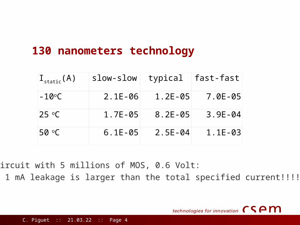
130 nanometers technology
Istatic(A) slow-slow typical fast-fast
-10oC 2.1E-06 1.2E-05 7.0E-05
25 oC 1.7E-05 8.2E-05 3.9E-04
50 oC 6.1E-05 2.5E-04 1.1E-03
Circuit with 5 millions of MOS, 0.6 Volt: - 1 mA leakage is larger than the total specified current!!!!!
C. Piguet :: 18.04.23 :: Page 5
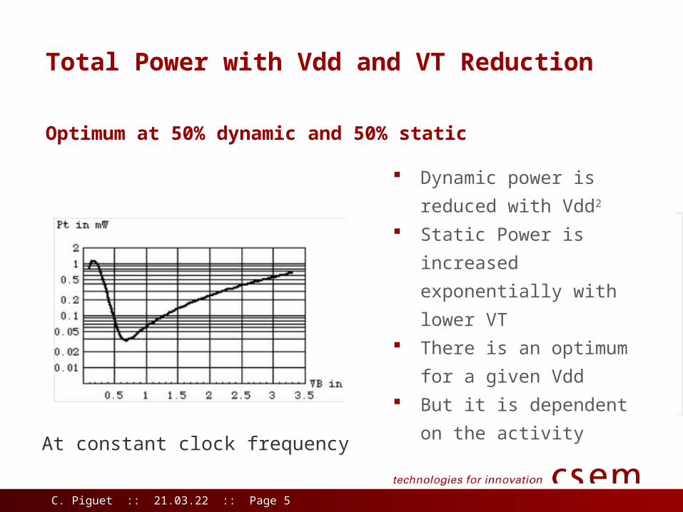
Total Power with Vdd and VT Reduction
Optimum at 50% dynamic and 50% static
Dynamic power is reduced
with Vdd2
Static Power is increased
exponentially with lower
VT
There is an optimum for a
given Vdd
But it is dependent on the
activity At constant clock frequency
C. Piguet :: 18.04.23 :: Page 6
Leakage Reduction Techniques
Portables devices, Ad-Hoc networks: very low activity
Leakage reduction factors of 100 are often required
Circuit: Several VT, Variable VT, Shut down
Gate: Stacked transistors, Input Vectors
Architecture: Very few innovative techniques (a low activity is far
from the optimum, the goal could be less transistors but higher
activity)
Techniques at Circuit, Gate and Architecture Levels
)1(0 nVbsVV THTH

C. Piguet :: 18.04.23 :: Page 7
Circuit Techniques I
Deep Submicron Technologies provide low and high VT
Low VT on the critical path, high VT elsewhere
10-20% of the gates are low VT (for industrial circuits)
Achieved reduction factor of about 10
Factor 7 for a processor of Hitachi
But factor 100 for its clock tree
Several VT or MTCMOS

C. Piguet :: 18.04.23 :: Page 8
Circuit Techniques II
Bias voltages on substrates
High VT in idle or low activity modes
Low VT for speed performances
Dynamic VT shift
Variable VT or VTCMOS or SATS
In deep submicron, the slope factor n is smaller and smaller
Larger bias voltages are required for smaller VT variations
SOI: the slope factor n is very close to 1
Problem
Vdd=2 V.VTp= -0.2 V. active modeVTp= -0.6 V. idle mode
VTn= 0.2 V. active modeVTm= 0.6 V. idle mode
Bias
2 V. active mode4 V. idle mode
0 V. active mode-2 V. idle mode
C. Piguet :: 18.04.23 :: Page 9
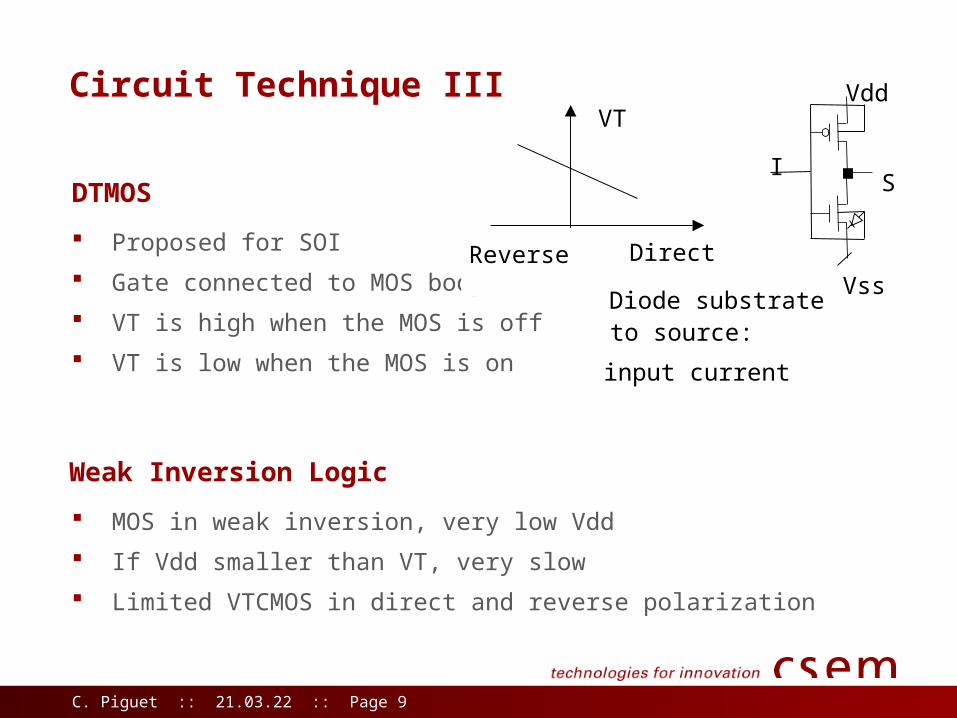
Circuit Technique III
Proposed for SOI
Gate connected to MOS body
VT is high when the MOS is off
VT is low when the MOS is on
DTMOS
MOS in weak inversion, very low Vdd
If Vdd smaller than VT, very slow
Limited VTCMOS in direct and reverse polarization
Weak Inversion Logic
Vdd
S
Vss
I
VT
Direct
Diode substrate to source:
input current
Reverse

C. Piguet :: 18.04.23 :: Page 10
Circuit Techniques IV
Switches in supply wires
Circuit voltage drop
High VT for switches, low VT for the circuit
Circuit MOS: source voltage at Vss’ higher than Vss: VT shift
But the voltage drop could be large, flip-flops loose their data
Shut down of the circuit (I)
circuitVss
Vss’>Vss
Vss
Vss’
Vss
Leakage
Switch size
Without switches
low VT
high VT
switches
Large Switches: - small leakage reduction
but large speed Small Switches: - the contrary
C. Piguet :: 18.04.23 :: Page 11
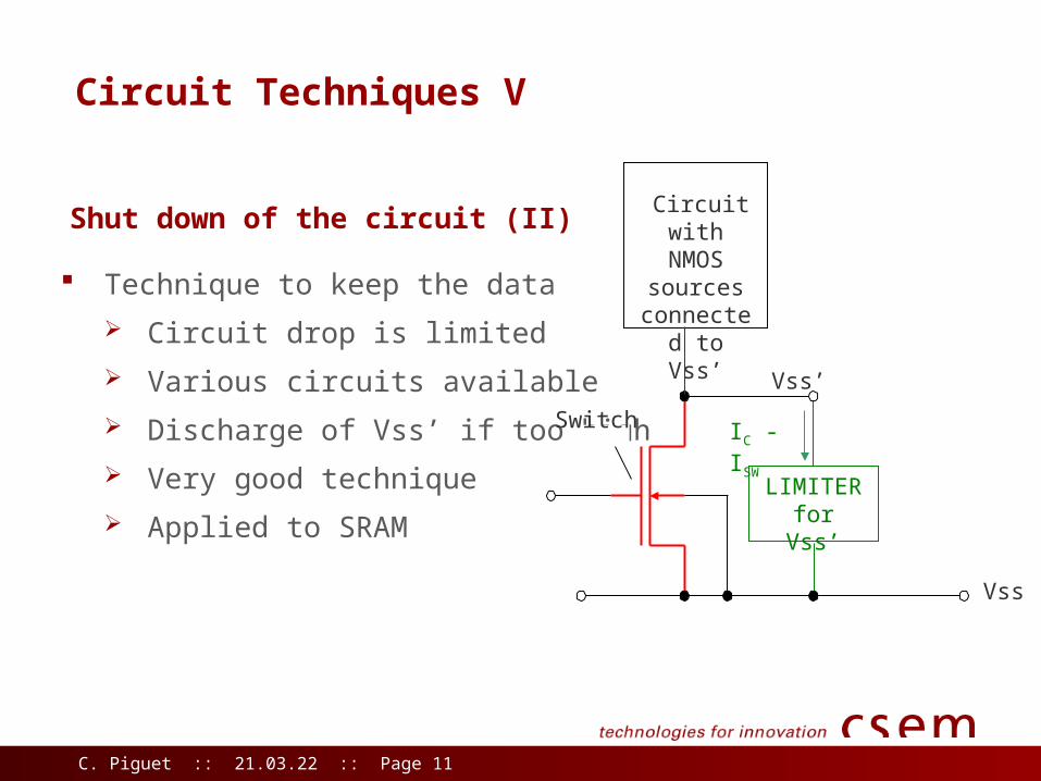
Circuit Techniques V
Technique to keep the data
Circuit drop is limited
Various circuits available
Discharge of Vss’ if too high
Very good technique
Applied to SRAM
Shut down of the circuit (II)
LIMITERfor Vss’
Circuit with NMOS sources
connected to Vss’
Vss
MNS
GS
IC - ISW
Vss’
Switch

C. Piguet :: 18.04.23 :: Page 12
Gate-Level Techniques
Just to list them:
Logic families when leakage is very different for N-ch and P-ch
N-MOS logic, or P-MOS logic, or precharge logic
Stacked transistors
A given input vector for a gate/circuit
Many techniques, but they do not achieve large leakage reduction
C. Piguet :: 18.04.23 :: Page 13
Architecture Techniques I
A low activity is detrimental for the ratio static over dynamic power
For a given logic function, various architectures
Is it possible for this logic function to reduce the number of
transistors (less leakage) by using more intensively the transistors,
i.e. by increasing the activity?
Are non-pipelined, pipelined, parallel, …, architectures better ?
Assuming that this logic function require 100 gate transitions, how
to design this function with the minimal number of MOS?
If 10’000 MOS, a= 1%; if 1’000 MOS, 1/10 leakage, same dynamic
power (100 transitions) but a=10%
Paradigm Shift
C. Piguet :: 18.04.23 :: Page 14
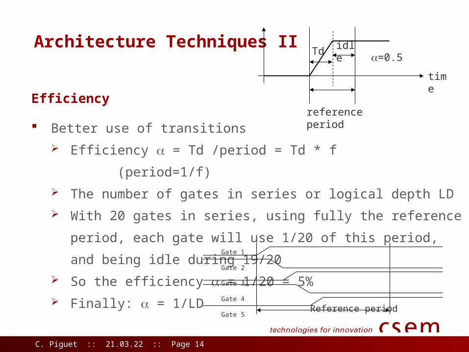
Architecture Techniques II
Better use of transitions
Efficiency = Td /period = Td * f (period=1/f)
The number of gates in series or logical depth LD
With 20 gates in series, using fully the reference period, each gate
will use 1/20 of this period, and being idle during 19/20
So the efficiency = 1/20 = 5%
Finally: = 1/LD
Efficiency
time
reference period
=0.5Td idle
Gate 1
Gate 2
Gate 3
Gate 4
Gate 5Reference period
C. Piguet :: 18.04.23 :: Page 15
Architecture Techniques III
Used for comparing architectures for a given logic function:
Activity a= nb of switching gates / total nb of gates
Efficiency = 1/LD or the logical depth = LD
The total number of gates N
Load capacitance C of a logic gate
IOFF leakage of a logic gate
ION dynamic power of a logic gate
Design parameters for designing an architecture
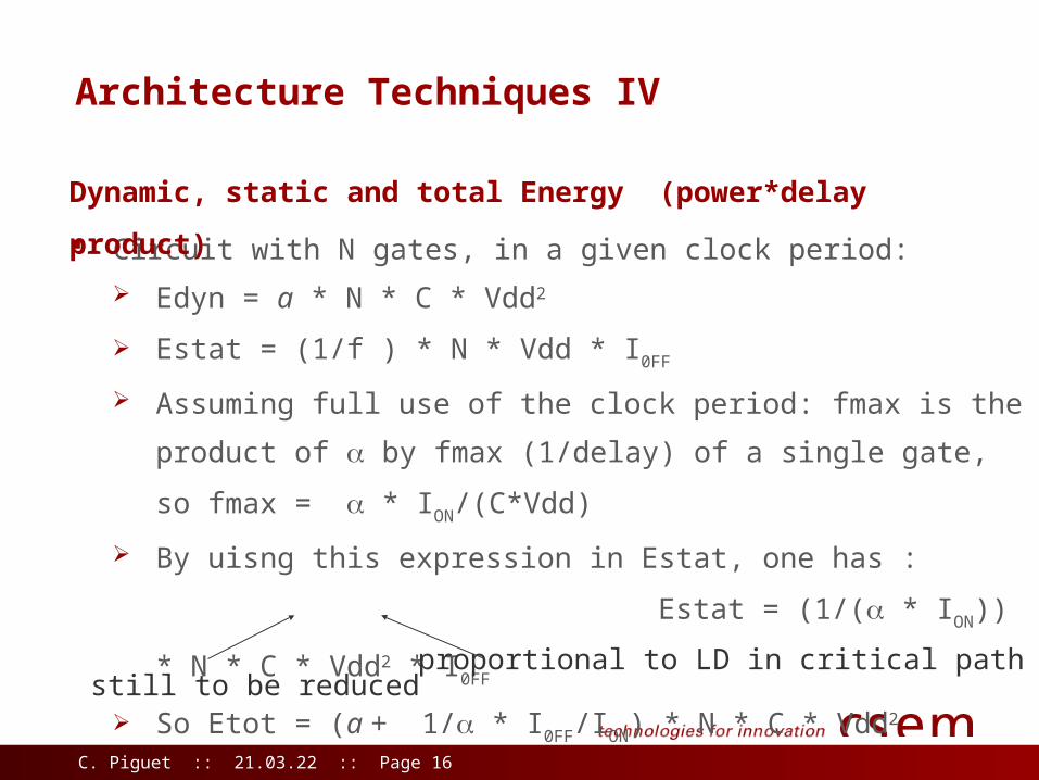
C. Piguet :: 18.04.23 :: Page 16
Architecture Techniques IV
Circuit with N gates, in a given clock period:
Edyn = a * N * C * Vdd2
Estat = (1/f ) * N * Vdd * I0FF
Assuming full use of the clock period: fmax is the product of by
fmax (1/delay) of a single gate, so fmax = * ION/(C*Vdd)
By uisng this expression in Estat, one has :
Estat = (1/( * ION)) * N * C * Vdd2 * I0FF
So Etot = (a + 1/ * I0FF/ION) * N * C * Vdd2
Dynamic, static and total Energy (power*delay product)
still to be reduced proportional to LD in critical path
C. Piguet :: 18.04.23 :: Page 17
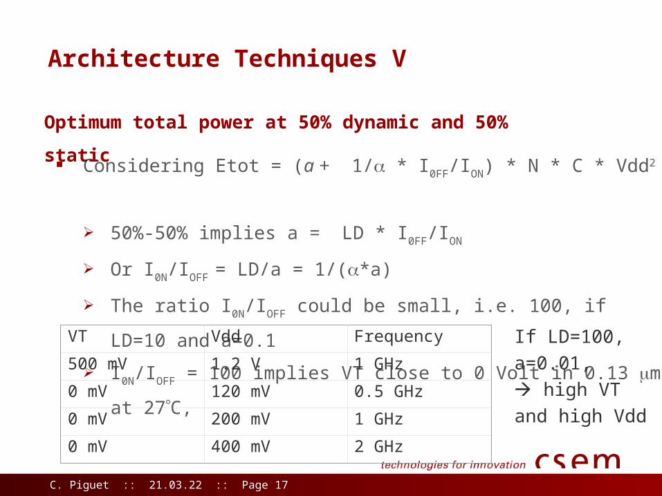
Architecture Techniques V
Considering Etot = (a + 1/ * I0FF/ION) * N * C * Vdd2
50%-50% implies a = LD * I0FF/ION
Or I0N/IOFF = LD/a = 1/(*a)
The ratio I0N/IOFF could be small, i.e. 100, if LD=10 and a=0.1
I0N/IOFF = 100 implies VT close to 0 Volt in 0.13 m at 27C,
Optimum total power at 50% dynamic and 50% static
VT Vdd Frequency
500 mV 1.2 V 1 GHz
0 mV 120 mV 0.5 GHz
0 mV 200 mV 1 GHz
0 mV 400 mV 2 GHz
If LD=100, a=0.01, high VT and high Vdd

C. Piguet :: 18.04.23 :: Page 18
Architecture Techniques VI
Assuming same
speed performances
VT Vdd Dynamic. Static Total
370 mV 1.5 33 mW 0 mW 33 mW
300 mV 1.25 25 mW 0 mW 25 mW
200 mV 0.97 15 mW 4 mW 19 mW
150 mV 0.83 10 mW 7 mW 17 mW
100 mV 0.7 8 mW 13 mW 21 mW
50 mV 0.55 7 mW 26 mW 33 mW
Power
0
5
10
15
20
25
30
35
50 100 150 200 250 300 370
Vdd
Po
we
r m
W
statique
dynamique
totale
[mV]

C. Piguet :: 18.04.23 :: Page 19
Architecture Techniques VII
To reduce drastically the total energy, one has to:
To reduce Vdd and VT (to have reasonable speed)
To have a low ratio I0N/IOFF , for instance 100
50% - 50% dynamic versus static, i.e. I0N/IOFF = LD/a
Logic depth LD and activity a are the design parameters
Architectures with small LD and high a
Design rules at the architecture level

C. Piguet :: 18.04.23 :: Page 20
Architecture Techniques VIII
To reduce LD and increase a:
Small LD requires pipelining or very fast architectures
High activity is confusing, as many techniques for reducing activity
have been proposed to reduce dynamic power
It is not a non-useful increase of activity, such as glitches
It has to be understood as reducing the total number of gates in the
activity = nb switching gates / total nb gates, by keeping constant
the number of switching gates (but activity depends also on modes)
Design parameters LD and a
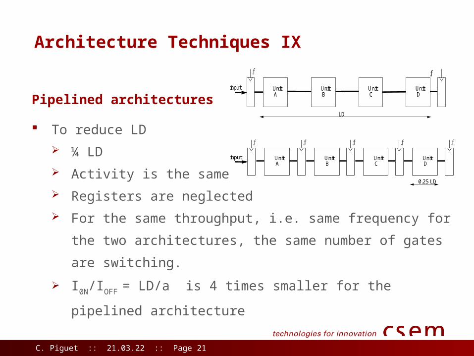
C. Piguet :: 18.04.23 :: Page 21
Architecture Techniques IX
To reduce LD
¼ LD
Activity is the same
Registers are neglected
For the same throughput, i.e. same frequency for the two
architectures, the same number of gates are switching.
I0N/IOFF = LD/a is 4 times smaller for the pipelined architecture
Pipelined architectures
input Unit A
ƒ ƒ
Unit B
Unit C
Unit D
LD
input Unit A
ƒ ƒ
Unit B
ƒ
Unit C
ƒ
Unit D
ƒ
0.25 LD
C. Piguet :: 18.04.23 :: Page 22
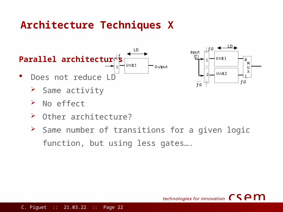
Architecture Techniques X
Does not reduce LD
Same activity
No effect
Other architecture?
Same number of transitions for a given logic function, but using
less gates….
Parallel architectures
Unit 1
Unit 2
input (ƒ)
M U X
ƒ/2
ƒ/2
ƒ/2
0
1
1
2
Unit 1
ƒ
Output 1
LD LD
C. Piguet :: 18.04.23 :: Page 23
Conclusion
Has to be considered at circuit, gate and architecture levels
Circuit Level: Reduction factors of about 100 achievable
Gate Level. Only moderate reduction factors
Architecture Level: to be checked
Back to the old time ?
When designers have to reduce the number of MOS, to re-use the
same units, serial architectures?
Leakage: Very important and interesting problem

T h a n k y o u f o r y o u r a t t e n t i o n.