Embed Size (px)
Citation preview
Design Methodology and Applications of SiGe BiCMOS Cascode Opamps with up to 37-GHz Unity Gain Bandwidth
Sorin P. Voinigescu1, Rudy Beerkens2, Timothy O. Dickson1, and Theodoros Chalvatzis1
1) ECE Dept., University of Toronto, 10 King's College Rd. Toronto, ON, M5S 3G4, Canada
2) STMicroelectronics, Ottawa, ON, Canada.
Abstract—A new technique to design highly stable operational amplifiers with maximum unity gain bandwidth, UGB, is developed. It relies on biasing MOSFETS at the peak fMAX current density. Several opamps, based on MOS-HBT SiGe BiCMOS cascodes, were designed and fabricated with UGB as high as 37 GHz. This record bandwidth is achieved with active p-MOSFET loads. A 1.3-GHz bandpass filter was implemented using two fully differential opamps with common-mode-feedback.
Keywords - operational amplifier, unity-gain bandwidth, cascode, SiGe BiCMOS, peak fMAX current density, bandpass filter, common-mode feedback
I. INTRODUCTION Traditional MOSFET opamp design relies on biasing the
transistors at a relatively low effective gate voltage of 0.1 to 0.2V. Apart from resulting in circuits with a relatively modest bandwidth, in sub-180nm technologies, this approach makes the opamp performance sensitive to threshold voltage and bias current variation. We report on a family of operational amplifiers (opamps) with record-breaking unity-gain bandwidth implemented in a 130-nm SiGe BiCMOS technology [1]. The fully differential opamps, featuring common-mode feedback, are based on a MOSFET-SiGe HBT cascode stage that proved to be optimal in high-speed CML/ECL [2] and millimeter-wave [3] applications. We now demonstrate that, when appropriately sized and biased, this topology (Fig. 1) results in highly linear, wideband amplifiers which require virtually no compensation to ensure good stability even at frequencies exceeding 20 GHz.
Figure 1. Opamp half-circuit schematic.
II. CIRCUIT DESIGN
It is well-known that the cascode stage with a MOSFET input and npn BJT output is ideal for realizing opamps with good stability [4]. Its main advantage over MOS-MOS or HBT-MOS cascodes stems from the complete elimination of the Miller effect, leading to an always stable, single-pole transfer function. The pole associated with the drain of the n-MOSFET and the emitter of the HBT is pushed to very high frequencies, at approximately fT,HBT. The latter easily exceeds 150 GHz in a state-of-the-art SiGe BiCMOS process and can therefore be ignored. For the circuit illustrated in Fig.1, the low frequency gain, dominant pole, and UGB can be described as
AV g m ,nMOS Rout UGBg m ,nMOS
2 Cout (1)
f p1
12 Rout C out
(2)
where Rout g m ,pMOS r o ,pMOS
2 (3)
Cout Cbc Ccs Cdb ,pMOS Cgd,pMOS CL (4)
In deriving (3) we have ignored the output resistance of the
nMOS-HBT cascode. Due to the much larger gm and ro of the HBT, it exceeds that of the pMOS cascode by more than an order of magnitude.
The second pole of the circuit is located at the gate of the n-MOSFET. It, too, can be pushed far beyond fp1 by employing a multi-finger transistor geometry (to reduce the gate resistance Rg) and a driver stage with low output resistance (such as an emitter or source follower) to act as a low-RS signal source.
f p2
12 Rg Rs Cgs Cgd
(5)
For the phase margin to be larger than 45o, fp2 must exceed UGB. It is important to note that, in the limit of negligible load capacitance (i.e. CL=0), fp2 becomes a technology constant. Furthermore, Cout/W is, to first order, invariant across technology nodes and foundries since it is dominated by the
VDD
= 3.3 V
VOUT
VIN
20*0.130µm*2µm
28*0.150µm*4µm
0.180µm*10µm
8..10 mA
VBIAS
= 1.8 V
CPAD
= 40 fF
CPAD
= 40 fF
Cdb and Cgd of the p-MOSFET, approximately 1 fF/µm and 0.3 fF/µm, respectively.
Beyond the choice of topology, the key to achieving record UGB is to bias the MOSFET at a large effective gate voltage where the I-V characteristics become linear rather than obey the classical square law [6]. More precisely, the MOSFET is biased at 0.2mA/µm, corresponding to the peak fMAX current density. Even though this regime is unconventional for opamp design because it results in somewhat reduced low-frequency gain, it leads to three favorable outcomes: (i) maximized UGB, (ii) maximized linearity, and (iii) UGB becomes insensitive to threshold voltage and bias current variation. This choice of bias point relies on the experimental observation that, in deep submicron MOSFETs, the optimum noise figure current density (0.15mA/µm), the peak fMAX current density (0.2mA/µm) [5], and the peak fT current density (0.3mA/µm) [5] remain largely invariant between foundries and technology nodes [6]. For the first time, we apply this observation to the algorithmic design of operational amplifiers using SiGe BiCMOS cascodes. To maximize the UGB of the opamp, all p- and n-MOSFETs and SiGe HBTs in the differential cascode stage are biased at their peak fMAX current density, while the DC gain remains above 34 dB.
The schematic of a fully differential opamp using the nMOS-SiGeHBT cascode with active p-MOSFET cascode load is shown in Fig. 2. Emitter followers Q5 and Q6 provide low output impedance and appropriate DC voltage levels to drive an identical stage. The common-mode feedback path, consisting of the degeneration resistors of Q5 and Q6 and of Q11 and Q12, operates as follows. If the common-mode DC voltage at VON and VOP rises, the current through Q11 increases, it is next mirrored by Q12 leading to a reduction in the common-mode voltage at the collectors of Q3 and Q4 and, finally, at VON and VOP.
Figure 2. Differential opamp schematic.
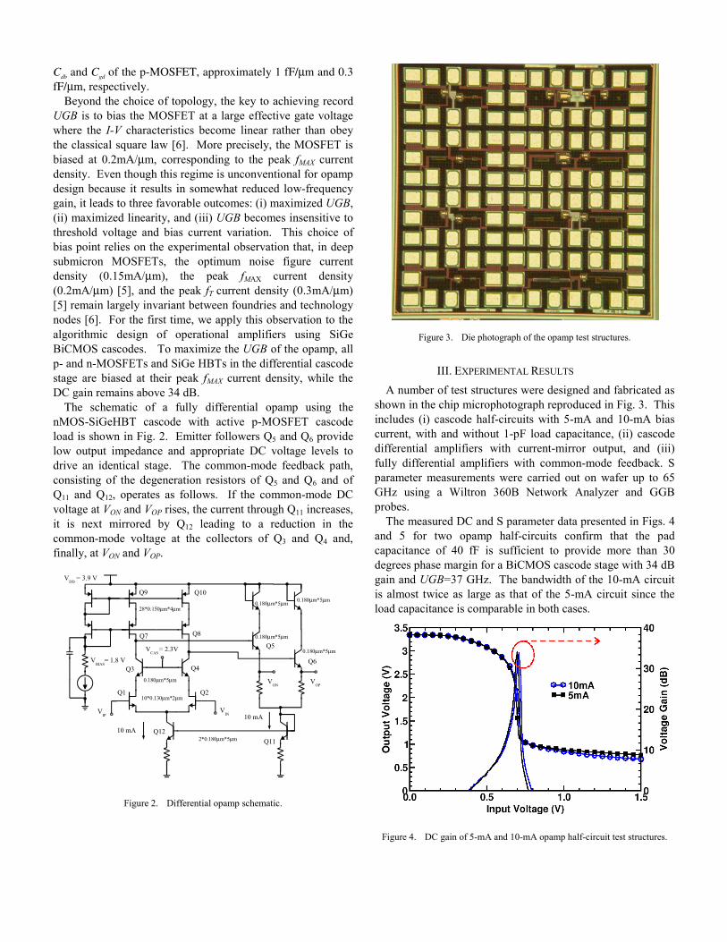
Figure 3. Die photograph of the opamp test structures.
III. EXPERIMENTAL RESULTS A number of test structures were designed and fabricated as
shown in the chip microphotograph reproduced in Fig. 3. This includes (i) cascode half-circuits with 5-mA and 10-mA bias current, with and without 1-pF load capacitance, (ii) cascode differential amplifiers with current-mirror output, and (iii) fully differential amplifiers with common-mode feedback. S parameter measurements were carried out on wafer up to 65 GHz using a Wiltron 360B Network Analyzer and GGB probes.
The measured DC and S parameter data presented in Figs. 4 and 5 for two opamp half-circuits confirm that the pad capacitance of 40 fF is sufficient to provide more than 30 degrees phase margin for a BiCMOS cascode stage with 34 dB gain and UGB=37 GHz. The bandwidth of the 10-mA circuit is almost twice as large as that of the 5-mA circuit since the load capacitance is comparable in both cases.
Figure 4. DC gain of 5-mA and 10-mA opamp half-circuit test structures.
VDD
= 3.9 V
VCAS
= 2.3V
VIP
10*0.130µm*2µm
28*0.150µm*4µm
0.180µm*5µm
10 mA
VBIAS
= 1.8 V
10 mAV
IN
VON
VOP
Q1 Q2
Q3 Q4
Q5
Q6
Q7 Q8
Q9 Q10
Q11Q12
2*0.180µm*5µm
0.180µm*5µm
0.180µm*5µm
0.180µm*5µm0.180µm*5µm
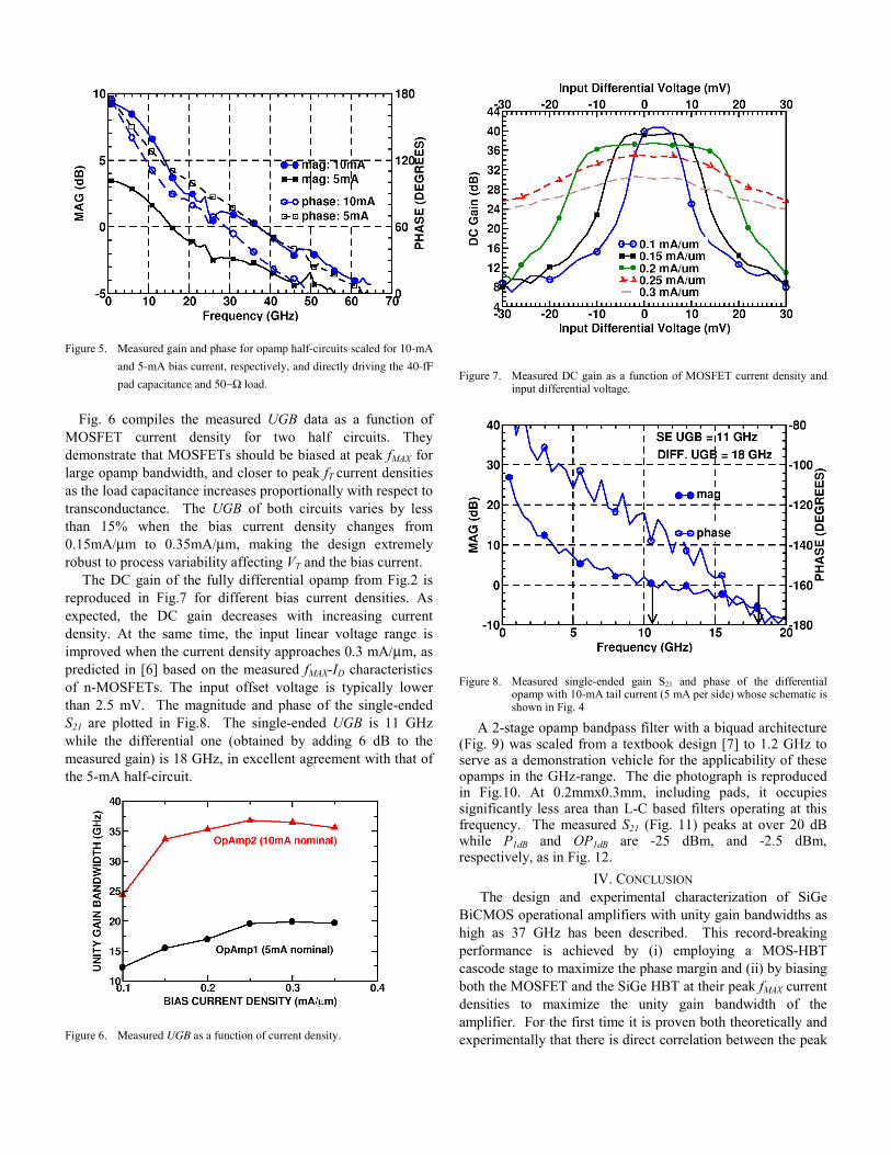
Figure 5. Measured gain and phase for opamp half-circuits scaled for 10-mA
and 5-mA bias current, respectively, and directly driving the 40-fF
pad capacitance and 50−Ω load.
Fig. 6 compiles the measured UGB data as a function of
MOSFET current density for two half circuits. They demonstrate that MOSFETs should be biased at peak fMAX for large opamp bandwidth, and closer to peak fT current densities as the load capacitance increases proportionally with respect to transconductance. The UGB of both circuits varies by less than 15% when the bias current density changes from 0.15mA/µm to 0.35mA/µm, making the design extremely robust to process variability affecting VT and the bias current.
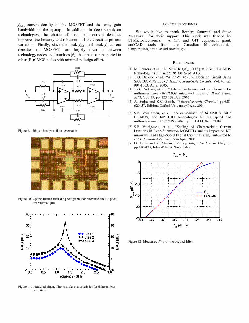
The DC gain of the fully differential opamp from Fig.2 is reproduced in Fig.7 for different bias current densities. As expected, the DC gain decreases with increasing current density. At the same time, the input linear voltage range is improved when the current density approaches 0.3 mA/µm, as predicted in [6] based on the measured fMAX-ID characteristics of n-MOSFETs. The input offset voltage is typically lower than 2.5 mV. The magnitude and phase of the single-ended S21 are plotted in Fig.8. The single-ended UGB is 11 GHz while the differential one (obtained by adding 6 dB to the measured gain) is 18 GHz, in excellent agreement with that of the 5-mA half-circuit.
Figure 6. Measured UGB as a function of current density.
Figure 7. Measured DC gain as a function of MOSFET current density and input differential voltage.
Figure 8. Measured single-ended gain S21 and phase of the differential
opamp with 10-mA tail current (5 mA per side) whose schematic is shown in Fig. 4
A 2-stage opamp bandpass filter with a biquad architecture (Fig. 9) was scaled from a textbook design [7] to 1.2 GHz to serve as a demonstration vehicle for the applicability of these opamps in the GHz-range. The die photograph is reproduced in Fig.10. At 0.2mmx0.3mm, including pads, it occupies significantly less area than L-C based filters operating at this frequency. The measured S21 (Fig. 11) peaks at over 20 dB while P1dB and OP1dB are -25 dBm, and -2.5 dBm, respectively, as in Fig. 12.
IV. CONCLUSION The design and experimental characterization of SiGe
BiCMOS operational amplifiers with unity gain bandwidths as high as 37 GHz has been described. This record-breaking performance is achieved by (i) employing a MOS-HBT cascode stage to maximize the phase margin and (ii) by biasing both the MOSFET and the SiGe HBT at their peak fMAX current densities to maximize the unity gain bandwidth of the amplifier. For the first time it is proven both theoretically and experimentally that there is direct correlation between the peak
fMAX current density of the MOSFET and the unity gain bandwidth of the opamp. In addition, in deep submicron technologies, the choice of large bias current densities improves the linearity and robustness of the circuit to process variation. Finally, since the peak fMAX and peak fT current densities of MOSFETs are largely invariant between technology nodes and foundries [6], the circuit can be ported to other (Bi)CMOS nodes with minimal redesign effort.
Figure 9. Biquad bandpass filter schematics
Figure 10. Opamp biquad filter die photograph. For reference, the HF pads
are 50µmx70µm.
Figure 11. Measured biquad filter transfer characteristics for different bias
conditions.
ACKNOWLEDGMENTS
We would like to thank Bernard Sautreuil and Steve McDowall for their support. This work was funded by STMicroelectronics. A CFI and OIT equipment grant, andCAD tools from the Canadian Microelectronics Corporation, are also acknowledged.
REFERENCES [1] M. Laurens et al., “A 150 GHz fT/fMAX 0.13 µm SiGe:C BiCMOS
technology,” Proc. IEEE BCTM, Sept. 2003. [2] T.O. Dickson et al., “A 2.5-V, 45-Gb/s Decision Circuit Using
SiGe BiCMOS Logic,” IEEE J. Solid-State Circuits, Vol. 40, pp. 994-1003, April. 2005.
[3] T.O. Dickson, et al., “Si-based inductors and transformers for millimeter-wave (Bi)CMOS integrated circuits,” IEEE Trans. MTT, Vol. 53, pp. 123-133, Jan. 2005.
[4] A. Sedra and K.C. Smith, “Microelectronic Circuits” pp.628-629, 5th. Edition, Oxford University Press, 2004
[5] S.P. Voinigescu, et al., “A comparison of Si CMOS, SiGe BiCMOS, and InP HBT technologies for high-speed and millimeter-wave ICs,” SiRF-2004, pp. 111-114, Sept. 2004.
[6] S.P. Voinigescu, et al., “Scaling of Characteristic Current Densities in Deep-Submicron MOSFETs and its Impact on RF, mm-wave, and High-Speed Digital Circuit Design,” submitted to IEEE J. Solid-State Circuits in April 2005.
[7] D. Johns and K. Martin, “Analog Integrated Circuit Design,” pp.420-423, John Wiley & Sons, 1997.
Figure 12. Measured P1dB of the biquad filter.
180 Ω
180 Ω
180 Ω
180 Ω
50 Ω
50 Ω
350 fF
350 fF 350 fF
350 fF
24 fF
24 fF
24 fF24 fFV
inV
out