Embed Size (px)
Citation preview
This document is downloaded from DR‑NTU (https://dr.ntu.edu.sg)Nanyang Technological University, Singapore.
Design methodologies and digital circuitimplementation for 3DIC wireless sensor node(WSN) system
Lan, Jingjing
2012
Lan, J. (2012). Design methodologies and digital circuit implementation for 3DIC wirelesssensor node (WSN) system. Master’s thesis, Nanyang Technological University, Singapore.
https://hdl.handle.net/10356/50626
https://doi.org/10.32657/10356/50626
Downloaded on 01 Feb 2022 22:51:39 SGT

DESIGN METHODOLOGIES AND DIGITAL CIRCUIT
IMPLEMENTATION FOR
3DIC WIRELESS SENSOR NODE (WSN) SYSTEM
LAN JING JING
School of Electrical & Electronic Engineering
A thesis submitted to the Nanyang Technological University
in fulfillment of the requirement for the degree of Master of Engineering
2012

i
Acknowledgements
First and above all, I would like to express my sincere gratitude to my supervisor Prof.
Goh Wang Ling for her guidance and continuous encouragement. Her knowledgeable
advices and guidance are indispensable for the completion of my candidature. The
knowledge and thoughts I have gained from her through the numerous discussions
will definitely benefit my future life. Besides constant encouragement, support and
guidance on my research, she also provided me a lot of opportunities to meet with
other leading experts from both the academia and the industry. She has given me a
wealth of knowledge and perspective.
I am indebted to Dr. Liu Xin, who brought me into the exciting three-dimensional
integrated circuit (3D IC) design exploration world and has guided me through my
research. His vision and ideas are primarily responsible for the research presented in
this work. His enthusiasm towards VLSI design is very inspiring and contagious. It
has been a great privilege to have been advised by him.
I am also particularly grateful to A*STAR IME ICS group and the 3D IC research
group members, Dr. Philippe Royannez, Ms. Mini Jayakrishnan and Dr. Wang Chao
for providing a conducive and productive environment. I am grateful to be a part of an
innovative project, a friendly working environment, and an enjoyable research group.
In addition, I would like to summarize my acknowledgements to the people who have
been supporting me on the work. I thank Prof. Yeo Kiat Seng and Prof. Kong Zhi Hui,
who brought me into the IC design world and has helped and guide me through my
study. I would probably never realize the beauty of VLSI if I had not talked with them.
I would also like to thank Mr. Zhu Ning, for his kind help in the course of the project.

ii
Lastly, I would like to thank anyone whom had participated in project discussion with
me, including those inside and outside Nanyang Technological University. Without
them, this dissertation would never have been accomplished.
Next, I thank Nanyang Technological University and A*STAR Institute of
Microelectronics, Singapore for providing me a great environment for education and
research.
Finally, I owe my deepest gratitude to my family members. I would like to give my
thanks to my parents for their love, encouragement and unconditional support. I am
grateful for their patience and trust they placed on me through all these years.
iii
Table of Contents Page
Acknowledgements i
Summary vi
List of Figures viii
List of Tables x
Chapter 1 Introduction 1
1.1 Background and Motivation 1
1.2 Research Objectives 6
1.3 Thesis Organization 7
Chapter 2 Literature Review 9
2.1 Three-Dimensional Integrated Circuit (3D IC) Technology 9
2.1.1 Die-to-Die Stacking 9
2.1.2 Die-to-Wafer Stacking 10
2.1.3 Wafer-Level Stacking 10
2.1.4 Through-Silicon Via (TSV) 11
2.2 Wireless Sensor Network 12
2.3 Wireless Sensor Node 15
2.4 IEEE Standard 802.15.4 19
Chapter 3 3D IC Design Methodology 23
3.1 Traditional Mixed-Signal IC Design Flow 23
3.2 3D IC Design Flow 25
3.2.1 Design Flow Impact of 3D Integration 26
3.2.2 3D Mixed-Signal IC Design Flow 28

iv
Chapter 4 3D Wireless Sensor Node 32
4.1 Wireless Sensor Node System Architecture 32
4.1.1 Sensing Subsystem 34
4.1.2 Analog Front-End Interface 35
4.1.3 Communication Subsystem 35
4.1.4 Power Management Subsystem 35
4.2 Digital Core Design 36
4.2.1 Transmitter (TX) 36
4.2.2 Receiver (RX) 48
4.3 3D Architecture 52
4.3.1 Design Exploration 52
4.3.2 Floor Planning 53
4.3.3 Place and Route 60
4.3.4 Physical Verification/Extraction 62
4.3.5 PCB Interface 63
4.3.6 3D Simulation 64
Chapter 5 FPGA Implementation and Functional Tests 68
5.1 FPGA Implementation 68
5.2 Functional Tests 69
5.2.1 Equipment 69
5.2.2 Test Setup 70
5.2.3 Results 73
Chapter 6 Conclusions and Future Work 78
6.1 Conclusions 78
6.2 Further Work 79
6.2.1 Early Planning and Estimation Tools for 3D IC Design 79
6.2.2 Low Power Digital Core Design 80

v
References 82
Publication List 88
Appendices 89
Appendix A: Verilog RTL code of ADC interface for transmitter 89
Appendix B: Verilog RTL code of ID generator for transmitter 93
Appendix C: Verilog RTL code of packet generator for transmitter 96
Appendix D: Verilog RTL code of microcontroller for transmitter 107
Appendix E: Verilog RTL code of SPI decoder for transmitter 129
Appendix F: Verilog RTL code of microcontroller for receiver 135
vi
Summary
In recent years, there is a great deal of interest in the three-dimensional integrated
circuit (3D IC). By stacking multiple active device layers with vertical interconnect,
3D IC technology provides great opportunities for designers to meet power and
performance requirements.
In this research, the innovative 3D IC technology is employed as a basic tool. In
addition to the conventional horizontal dimension, active devices are stacked in the
vertical dimension in 3D IC technology. The additional degree of connectivity in the
vertical dimension enables circuit designers to replace long horizontal wires with
short vertical interconnects, so that delay, power consumption, and area can be
reduced. The design problem of miniaturized wireless sensor node has been explored
and a digital core design in wireless sensor node is proposed in this work. The design
aims to provide an efficient solution for recording users’ bio-vital data, as well as to
transmit, extract and deposit the information on the platform. This capability serves to
monitor the progression of chronic diseases. The 3D architecture for a wireless sensor
node will be discussed in-depth and the impact of 3D-integration technology on
conventional digital circuit design will be demonstrated in this project too. Through
silicon via (TSV) based 3D integration technology is employed as the vertical
interconnect methodology. The proposed design methodologies described in this
thesis are intended to strengthen the 3D design capabilities, making this fascinating
technology a promising solution for future integrated systems.
Functional tests were conducted to validate the overall systems usability and
modularity and the measured results proved that reliable data transfer and continuous
bio-vital data monitoring can be consistently achieved. The measured results validated

vii
the approaches chosen, and verified that the system is useful in patient monitoring
application. The next phase of the work will be to implement the proposed digital core
design in 3D wireless sensor node in field programmable gate array (FPGA).
viii
List of Figures
Figure 1.1: A 3D integration system [18]. .............................................................................. 3
Figure 2.1: The example of die-to-die stacking [49]. ............................................................ 9 Figure 2.2: One example of die-to-wafer stacking. ............................................................. 10 Figure 2.3: One example of wafer-to-wafer stacking [51]. ................................................. 11 Figure 2.4: 3D structure using through-silicon-via interconnects [52]. ............................ 11 Figure 2.5: A medium access protocol for wireless sensor network [64]. ......................... 13 Figure 2.6: A typical structure of a wireless sensor node. .................................................. 15 Figure 2.7: The 2450 MHz PHY modulation and spreading functions [96]. .................... 20 Figure 2.8: O-QPSK chip offsets [96]. ................................................................................. 21
Figure 3.1: A mixed-signal circuit design flow. ................................................................... 23 Figure 3.2: The traditional digital IC design flow. ............................................................. 24 Figure 3.3: An example of a high-level view of the 3D IC design flow [99]. ..................... 25 Figure 3.4: A 3D IC integrated disparate fabrication technologies [100]. ........................ 26 Figure 3.5: An example of TSV structure............................................................................ 27 Figure 3.6: An overview of the design flow used in this work. .......................................... 29
Figure 4.1: System architecture of wireless sensor node. ................................................... 33 Figure 4.2: System schematic of wireless sensor node. ...................................................... 33 Figure 4.3: Blood pressure sensor acquisition designs. ...................................................... 34 Figure 4.4: Power distribution of wireless sensor node. ..................................................... 36 Figure 4.5: Transmitter digital core block diagram. .......................................................... 37 Figure 4.6: ADC timing diagram. ........................................................................................ 38 Figure 4.7: The internal structure of two of the FIFOs. .................................................... 39 Figure 4.8: Typical CRC module implementation [96]. ..................................................... 40 Figure 4.9: Format of the PPDU. ......................................................................................... 42 Figure 4.10: Format of the SFD field [96]. .......................................................................... 42 Figure 4.11: State diagram of microcontroller. ................................................................... 45 Figure 4.12: SPI interfaces of baseband and microcontroller. .......................................... 46 Figure 4.13: Illustration of SPI command timing waveform. ........................................... 47 Figure 4.14: Block diagram of receiver microcontroller. ................................................... 50 Figure 4.15: State diagram of microcontroller in receiver part. ....................................... 51 Figure 4.16: Block diagram of the Wireless Transceiver. .................................................. 53 Figure 4.17: Transmitter digital core block diagram after optimization.......................... 56 Figure 4.18: 3D architecture of wireless sensor node. ........................................................ 60 Figure 4.19: Cross section of the die for via last TSV process. .......................................... 61 Figure 4.20: Layout of one die including TSVs and bumps (from A*STAR IME ICS
Group). ........................................................................................................................... 62
ix
Figure 4.21: 3D IC Stacking Strategy for the bottom die. ................................................. 64 Figure 4.22: Simulation results of RF receiver noise response with and without TSV
(from A*STAR IME ICS Group). ................................................................................ 65 Figure 4.23: Simulation results of RF receiver signal response with and without TSV
(from A*STAR IME ICS Group). ................................................................................ 65 Figure 4.24: RF transmitter performance with TSV and RDL layer capacitance (from
A*STAR IME ICS Group). .......................................................................................... 66 Figure 4.25: Post-layout simulation results of RF transmitter VCO and PA outputs: (a)
2D implementation; (b) 3D implementation with TSV macro (from A*STAR IME ICS Group). ................................................................................................................... 66
Figure 4.26: System architecture of the proposed 3D IC integration WSN system......... 67
Figure 5.1: FPGA board used in this design: (a) Xilinx Virtex-5; (b) Xilinx Spartan-3E.......................................................................................................................................... 68
Figure 5.2: Test equipment: (a) Agilent logic analysis system; (b) HP DC source. .......... 70 Figure 5.3: PCB boards used in the tests: (a) Receiver; (b) Voltage divider; (c)
Transmitter. ................................................................................................................... 71 Figure 5.4: Functional tests setup of digital core design. ................................................... 71 Figure 5.5: Final tests platform setup of digital core design. ............................................ 72 Figure 5.6: The result window of the logic analyzer. .......................................................... 74 Figure 5.7: TX operation after TX_EN on: (a) Test result; (b) Simulation result. .......... 75 Figure 5.8: RX_READ from receiver to digital core: (a) Test result; (b) Simulation
result. .............................................................................................................................. 76 Figure 5.9: Continuous 8-bits parallel output: (a) Test result; (b) Simulation result. ..... 77

x
List of Tables
Table 2.1: Symbol-to-chip mapping [96] ............................................................................. 21
Table 4.1: IO statistics of each portion in 3D ICs ............................................................... 54 Table 4.2: IO statistics of each portion in 3D ICs after digital core architecture
optimization ................................................................................................................... 55 Table 4.3: TSV statistics of each layer in 3D ICs with SC, PM, DIG, IF, RF order ......... 58 Table 4.4: TSV statistics of each layer in 3D ICs with SC, DIG, PM, IF, RF order ......... 59
Table 5.1: Transmitter digital design resource usage ......................................................... 69 Table 5.2: Receiver digital design resource usage ............................................................... 69

1
Chapter 1 Introduction
1.1 Background and Motivation
Continuing advancements in semiconductor technology have made sure that the
integrated circuit (IC) industry continues to follow the Moore’s law. This has been
possible due to the endless scaling of CMOS transistor size and innovations in
packaging. The scaling of transistor size results in increased frequency response of the
transistors, which in turn produces faster circuits.
Due to aggressive scaling of process technologies, circuit feature sizes are able to
shrink continuously. With improvement of the performance of gates, interconnects
have become one of the major performance bottlenecks [1, 2]. Because the global
interconnects do not scale accordingly with process technologies. An enormous
amount of effort is needed to further scale the dimensions in deep submicron
technologies. As technology scaling is slowing down and design complexity is already
extremely high, the capacity of improving performance through scaling or adding
more complexity is limited. However, in order to meet performance, heterogeneous
integration, cost, and size demands, recently the three-dimensional (3D) integration
technology has emerged as a leading contender in this challenge through this decade
and beyond.
The 3D-integration technology is a new technology that has the potential to address
many of the challenges the semiconductor industry faced. In a conventional planar
(2D) technology, floor-planning and layout constraints may force two connected
circuits to be physically separated, thus global wires are required for communication.

2
However, in a 3D architecture, these circuits can be stacked on top of each other. So
that the long global wires can be replaced with short vertical interconnects. Vertical
stacking of multiple die within a package, using specialized substrates and
interconnects, will also reduce the number of chip-to-board connections and decrease
the area required for chips and inter-chip wire traces. These techniques are also
advantageous from a power consumption standpoint since 40% of power consumption
comes from chip-to-chip interconnects. The module-to-board solder connects account
for almost 90% of board failures. Hence, reducing the number of connections can
decrease board failures and attain an overall increase in reliability and decrease in
power consumption [3, 4]. 3D integration technology also provides increased device
density, reduced latency, and lower power [5-12]. Due to vertical connectivity each
transistor can access a greater number of adjacent transistors leading to higher
bandwidth [13].
The three-dimensional integrated circuit (3D IC) technology is a technology that
stacks multiple layers of silicon together with vertical interconnects between them to
create an IC that has active devices on more than one silicon layers. More importantly,
3D IC technology enables the possibility to integrate components of different
fabrication technologies. Overall, 3D IC technology provides a wreath of advantages
over traditional 2D IC technology; where some of them will be described in the
following sections.
1. Miniaturization
One major advantage of 3D ICs is the reduction of chip area. Studies showed that 3D
integration can significantly reduce the interconnect wire length between the blocks as
compared to its 2D counterpart [14, 15]. By repartitioning the functional blocks into
different layers and optimizing each layer with the most suitable technologies, it
enables the possibility of reducing the chip area [16, 17]. Figure 1.1 illustrates an
example of this process.

3
Figure 1.1: A 3D integration system [18].
2. Energy efficiency
Another obvious advantage of 3D ICs is power and energy reduction. As
interconnects consume a large portion of the total chip’s power [19], reduction on the
amount of interconnects will translate into power saving in 3D IC design. Different
studies demonstrated that energy efficient can be achieved using 3D stacking
technology [20-22].
3. Reliability
Reliability is an obstacle for wireless communication network. Due to practical issues
such as limited hardware and challenging environments, the wireless communication
will be prone to failure. Because of the reduction of interconnect wire length and
having shorter interconnect in the critical path [23], less parasitic RC delay and higher
performance can be achieved using 3D IC technology [20, 24, 25].
The relative benefits of the 3D-integration technology will continue to surge in future
technology generations, which making it a very attractive option for future circuit
designs. However, although 3D ICs offer several advantages over traditional 2D
Source: SAMSUNG

4
counterpart and it attracts substantial attentions from industry and academia, they still
face several challenges before they can be developed into viable commercial products.
First, there is no design methodology and Electrical Design Automation (EDA) tool to
support the 3D IC design. It is a complicated task with many ramifications to develop
a design flow for the 3D ICs. In order to be successfully evolved into a mainstream
technology, a number of challenges at each step of the design process have to be met
for 3D ICs. Due to the many impediments in the vertical dimension, the existing 2D
circuit design methodology cannot be simply extended to the 3D design. In order to
effectively realize large scale 3D IC systems, design methodologies at the front end
and mature manufacturing processes at the back end are collectively required. New
efficient design flows and algorithms must be developed before the adoption of 3D
IC.
Second, most of the researchers only focus on the physical aspect of the whole 3D IC
design, such as the 3D floor-plan, 3D placement and routing, 3D RC extraction, 3D
DRC, and LVS, while the front-end design remains the same as the traditional 2D
design. That means different function blocks of the chip is designed separately and
has little consideration for each other before they are fabricated on different tiers. In
other words, one tier may have the memory while the other may have the functional
units of the original design, and finally just bonded them together. For example, a
sensor array circuit was designed and implemented by researchers from MIT Lincoln
Lab [1] with SOI 3D processing technology. For every pixel, an analog to digital
converter (ADC) on one wafer and a photodiode on the other wafer was included. The
two parts were joined by a through via. The possibility of stacking circuits to build 3D
ICs with vertical interconnects was shown by this work. However, these studies did
not explore the potential 3D IC design space benefits at the architectural level before
chip is fabricated on different tiers. System architectural optimization during the
front-end design can result in better performance and smaller area consumption of 3D
IC. Thus, in order to make full use of all benefits of 3D design, significant effort is
5
required first at the front-end design.
Third, recently, there has been a great deal of interest in the 3D ICs, such as
3D-integrated caches [5-7, 26, 27], 3D-integrated register files [28], 3D-integrated
arithmetic units [12, 24-26], 3D-integrated content addressable memories (CAMs)
circuits [10, 11], clocking schemes for 3D-integrated circuits [29], 3D-integrated
processors [11, 21, 22, 30-33], 3D-integrated systems-on-a-chip [34, 35],
3D-integrated FPGA [36-38] and design automation tools for 3D-integrated designs
[11, 35, 39-42]. However, little mixed-signal 3D-integrated system which includes
analog, digital and radio frequency circuits is reported. One of the best examples of
the 3D-integrated system comes from B. Black et al [43], in which a microprocessor
chip was fabricated to evaluate the impact of 3D IC technology. The chip was
fabricated on two tiers and then bonded together face to face. However, no radio
frequency circuits are included. Since in a typical wireless communication system,
digital, analog and radio frequency circuits are the must, therefore, significant effort is
still required if 3D IC are to be used to design applicable wireless communication
system. One of the key advantages and differences the 3D integration provides is the
ability to integrate disparate fabrication technologies without disrupting the existing
process flows. Therefore, as the fabrication of 3D architecture becomes feasible, new
opportunities brought by 3D technology can result in innovations and in new
architectures for future many-core chip multiprocessor (CMP).
By stacking multiple active device layers with vertical interconnect, 3D IC technology
provides great opportunities for designers to meet power and performance
requirements. Compared to traditional two-dimensional integrated circuit (2D IC)
technology, the 3D IC technology allows denser integration and system size reduction,
lower power consumption, as well as shorter global interconnects and performance
improvement [2, 14]. It offers great opportunities for heterogeneous SOC integration
[11]. Overall, 3D IC technology provides a wreath of advantages over traditional 2D
IC technology.

6
1.2 Research Objectives
The main objective of this research is to develop a standard design flow for the 3D
ICs. 3D IC design methodology is a relatively new topic. Although researchers have
investigated several aspects for 3D integration such as floor-planning, placement and
routing [7, 44-46], no standard design flow has been reported in this area. Significant
effort is still required if they are to be used to design applicable 3D system. Since
there is no commercial 3D Electrical Design Automation (EDA) tool to support 3D IC
design, existing 2D design flow are to be utilized to assemble an efficient and reliable
flow for 3D ICs. In addition, the flow should minimize format changes by adopting
standard input/output file formats. Therefore, in this project, the 3D design
methodologies are explored based on the existing 2D design methodologies.
The second key objective of this research is to explore solution to address the space
exploration challenges faced by the 3D IC design during front-end design. The design
space exploration at the architectural level is crucial to take full advantages of 3D
integration. Therefore, as the fabrication of the 3D architecture becomes feasible, it is
desirable to develop a corresponding 3D architecture so that the designers can explore
the potential 3D IC design space and benefits at the architectural level. The front-end
design methodologies and the necessary differences between 3D ICs and traditional
2D ICs are therefore studied in this project.
The advantages brought by the 3D IC technology can result in innovations—in
creating new architectures for future circuit design. In the case of homogenous
integration, 3D IC technology provides increased computational power and reduced
wiring. While heterogeneous integration provides the possibility of different
technologies integration that may be more suitable for RF and mixed-signal circuits.

7
Therefore, the third objective of this research is to develop the architecture for a
typical wireless communication system, which includes digital, analog and radio
frequency circuits. With the constant increase in the aging population over the past 50
years, health care has become a major concern. Therefore, a miniaturized wireless
blood pressure sensor for patient monitoring applications is chosen to be implemented
in this research. To develop miniaturized wireless sensors, most of the existing
research works focus on arriving at low-power circuit and energy harvesting
techniques [47, 48]. A different approach, which is to minimize the sensor area via the
3D IC technology, is explored in this research. Adopting the ideas and techniques in
3D IC in the design of the wireless sensor node, a novel and innovative type of
wireless sensor node—3D wireless sensor node has been designed and this is one of
the major contribution of the thesis.
1.3 Thesis Organization
This chapter gives a brief overview of the 3D IC technology. The technical
background and motivation of 3D IC technology that helps in the understanding of
this project has been described. The advantages, potential problems associated with
the 3D IC technology as well as the research objective are provided. The rest of the
thesis is organized as follows.
Chapter 2 summarizes the current state of the art in 3D IC research and applications,
the 3D IC technology, and the 3D stacking technology. Literature survey and the
recent works on wireless sensor networks and the important application domains are
introduced next. Different aspects of the wireless sensor network applications, and the
challenges associated with these applications will be discussed. Finally, the relevant
IEEE Standard 802.15.4 requirements for operation in the 2.4 GHz band are
summarized.

8
In chapter 3, the 3D IC design methodologies and the advantages gained over
traditional 2D IC design will be studied. The chapter begins by comparing the
conventional 2D IC design flow with 3D IC flow to show the compatibility. Next, the
flow assembly and explanation of the sub-steps of the flow are discussed.
Chapter 4 presents detailed description of the proposed design. The design of
individual parts of the wireless sensor node will also be described. In chapter 4, a 3D
wireless sensor node architecture based on the proposed methodology for TSV
optimization is analyzed. The number of TSV in each layer is calculated and
evaluated under various conditions.
Validation experiments and performance analysis are provided in chapter 5. Test
results are shown to reiterate the validation of functionality of the system. Chapter 5
also provides a comparison of the measured results with simulation results. Details on
the test setup, test boards and software used to test the chips are also outlined.
Finally, chapter 6 summarizes the conclusion of the work and discusses on the future
work.

9
Chapter 2 Literature Review
2.1 Three-Dimensional Integrated Circuit (3D IC) Technology
3D IC technology reduces the chip area and length of interconnect wires without
scaling down the transistor sizes. A number of technologies have been explored to
carry out 3D integration, such as die-to-die stacking, die-to-wafer stacking and
wafer-to-wafer stacking.
2.1.1 Die-to-Die Stacking
In the die-to-die stacking method [49], independently fabricated stand-alone chips are
stacked on top of each other. Most commonly, the stacked chips are attached together
using bump or wire bonding or some flip-chip techniques. The example of die-to-die
stacking is illustrated in Figure 2.1.
Figure 2.1: The example of die-to-die stacking [49].
10
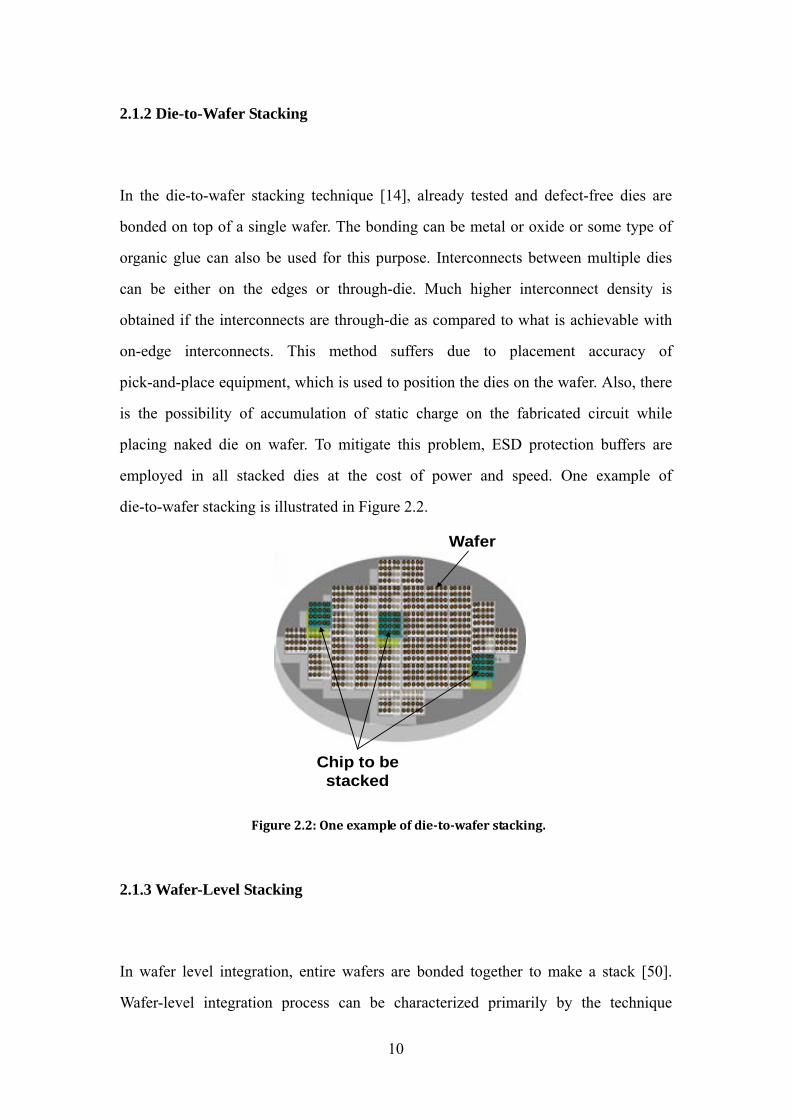
2.1.2 Die-to-Wafer Stacking
In the die-to-wafer stacking technique [14], already tested and defect-free dies are
bonded on top of a single wafer. The bonding can be metal or oxide or some type of
organic glue can also be used for this purpose. Interconnects between multiple dies
can be either on the edges or through-die. Much higher interconnect density is
obtained if the interconnects are through-die as compared to what is achievable with
on-edge interconnects. This method suffers due to placement accuracy of
pick-and-place equipment, which is used to position the dies on the wafer. Also, there
is the possibility of accumulation of static charge on the fabricated circuit while
placing naked die on wafer. To mitigate this problem, ESD protection buffers are
employed in all stacked dies at the cost of power and speed. One example of
die-to-wafer stacking is illustrated in Figure 2.2.
2.1.3 Wafer-Level Stacking
In wafer level integration, entire wafers are bonded together to make a stack [50].
Wafer-level integration process can be characterized primarily by the technique
Wafer
Chip to be stacked
Figure 2.2: One example of die-to-wafer stacking.

11
employed for bonding independent wafers, and also by the method of forming
inter-wafer interconnections. One example of wafer-to-wafer stacking is illustrated in
Figure 2.3.
Figure 2.3: One example of wafer-to-wafer stacking [51].
2.1.4 Through-Silicon Via (TSV)
The 3D packaging technology currently used is differentiated from the 3D integration
technology. Figure 2.4 shows assembled 3D structure using through-silicon-via
interconnects.
Figure 2.4: 3D structure using through-silicon-via interconnects [52].
In TSV technology based 3D IC chips, multiple active device layers are stacked
together through die stacking or wafer stacking with direct vertical TSV interconnects
[11]. Due to the adoption of TSVs at the micron scale, it provides miniaturization as
well as performance improvement over the traditional 2D systems. It comprises wire
bonded, flip chip bonded, edge connected or flex-connected chip stacks. 3D
12
packaging has the advantage of small form factor, hence is widely used in
telecommunication and consumer electronics. However, it does not provide the
shortest connections from each chip since signal and power need to be distributed
through long wires or have to be routed to the chip edges. 3D ICs have emerged as a
promising means to mitigate these interconnect-related problems [7, 11, 27, 44, 46,
53-58]. With more and more 3D research recently, the industry refers to the 3D
stacking technology utilizing through-silicon vias (TSVs). TSV 3D integration has the
potential to offer the greatest vertical interconnects density. Therefore it is the most
promising one among all vertical interconnect technologies.
2.2 Wireless Sensor Network
In recent years, the demand for long-term healthcare monitoring outside the hospital
has risen considerably. As one of the efficient solutions, the wireless sensor networks
technology has become the interest of researchers both from academia and industry
perspective [59].
Enabled by recent advances in the sensing and wireless communication technology,
wireless sensor networks are network systems capable of sensing and communicating
within short range. This approach distributes a large set of sensors over a wide area of
interest. The motivation of using wireless sensor networks is the ease of deployment
as no wiring is required. Batteries and energy harvesting are used in wireless sensor
networks. With appropriate configuration, such networked sensors can collaborate to
accomplish the tasks of monitoring physical or environmental condition such as light,
temperature and pressure.
Wireless sensor networks consist of nodes integrating modest amounts of computation,
storage, and communication capabilities. Low-power microprocessors, radios, and
13
MEMS sensors enable embedded sensing. The earliest research efforts on wireless
sensor networks date back to the late 1990's, when the United States Defense
Advanced Research Project Agency (DARPA) focused on developing low-power
sensing devices to enable large-scale, distributed, networked sensor systems. Since
then, numerous research and commercial efforts, such as the WINS [60] and
Sensorsim [61] from UCLA, Smart Dust [62] and PicoRadio [63] from UC Berkeley
have advanced the field from traditional simple low data-rate environmental
monitoring applications, to more complex ones ranging from smart-homes and factory
automation, to high data-rate mission-critical applications, such as
security-surveillance, structural health monitoring, and health-care.
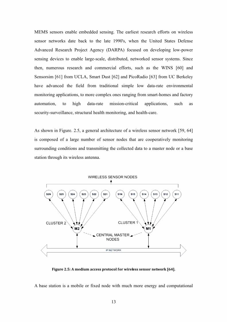
As shown in Figure. 2.5, a general architecture of a wireless sensor network [59, 64]
is composed of a large number of sensor nodes that are cooperatively monitoring
surrounding conditions and transmitting the collected data to a master node or a base
station through its wireless antenna.
Figure 2.5: A medium access protocol for wireless sensor network [64].
A base station is a mobile or fixed node with much more energy and computational

14
capability. It can link the wireless sensor network to an existing communications
network where the user can see the collected data. Therefore, in the healthcare
monitoring cases, patients can be located away from the hospitals and health centers.
Their collected bio-vital data is first transmitted wirelessly to the base station close to
them. The base station then transmits all real-time information received from sensors
to the health centers through the Wireless Local Area Network (WLAN). The system
should be able to immediately notify the patients or hospitals by sending proper
messages or alarms during such emergency through the wireless sensor network.
When appropriately deployed, this sensor network would allow real-time patients
monitoring all over the world. The combination of features together shall create a
wireless sensor network system.
Wireless sensor networks have many applications such as habitat monitoring [65-69],
environmental monitoring [70, 71], structural health monitoring [72, 73] and military
surveillance [74]. One important application of the wireless sensor networks is
patients’ monitoring. The system will monitor patients’ bio-vital parameters and report
to medical health centers for assistance in diagnosis [75]. One of these significant
bio-vital parameters is blood pressure. If a person's blood flows through their arteries
at too high pressure, they could be in danger even when they are lying on a sofa [76].
Too high a blood pressure will cause the heart to constantly pump at full speed, which
strains both the heart and vessel walls. Some drugs can help the patient temporarily,
but in many cases it is still difficult to regulate the patient's blood pressure. Also,
illnesses such as heart attack can suddenly happen without prior symptoms. But it
may be detected by blood pressure monitoring before the problem appears. Thus the
blood pressure has to be consistently monitored over a long period of time. This is a
burden for the patients where they have to wear a device containing the blood
pressure meter close to their bodies. An inflatable sleeve records their blood pressure
will be placed on their arms. Wireless sensor node can replace all the above processes
with a continuous implantable blood pressure monitoring system that will desirably
help in hypertension diagnosis and heart attack detection.

15
2.3 Wireless Sensor Node
Every node in a wireless sensor network usually consists of sensing hardware, limited
capability processor, memory, radio transceiver and energy source. A typical structure
of a wireless sensor node is illustrated in Figure 2.6 [77], and is described as follows:
1. Sensors and Front-end: The sensing unit collects data such as temperature, light and
pressure from the surrounding environment where the sensor is deployed. Then it
converts this data into electric signals which can be stored in memory. The specific
sensors used in each wireless sensor node are dependent on their applications.
Primarily, only low-data-rate sensing is supported due to bandwidth and power
constraints.
2. Embedded Processor: The processing unit performs some simple information
processing such as data compression and signal control. The computational capability
Figure 2.6: A typical structure of a wireless sensor node.

16
of these embedded processors is often significantly constrained. In order to achieve
significant energy savings, low-power circuit design techniques such as voltage
scaling are often used.
3. Memory: After the sensors capture the data from the surrounding environment, the
collected data is stored in memory. Traditionally the storage is mainly in the form of
random access memory (RAM) and read-only memory (ROM). However, since the
development of the flash memory, the data storage in memory has improved
significantly over the years.
4. Radio Transceiver: Wireless sensors nodes are often equipped with a low-rate,
short-range wireless radio transmitter. The wireless communications unit allows every
sensor node to send data to a processing center for further analysis. The
communication devices are often the most power-consuming components in a
wireless sensor node.
5. Power Source: Wireless sensor nodes are typically battery powered. However,
improvements of energy harvesting techniques may provide part of the energy in
some cases.
With all the above components integrated on board, wireless sensor nodes can be
deployed to accomplish tasks such as the environmental monitoring and patient
monitoring [78]. Each node collects data via its sensing units and sends out the data
through its wireless antenna. However, the limited transmission range of wireless
sensor nodes makes it impossible to transmit data in a long distance. Thus, the data is
first sent to a master node or an external processing machine having higher computing
power called the base station.
In the past few years wireless sensors have grown rapidly in their capabilities, e.g., a
descendant of the original UC Berkeley Mica "mote" sensor node [79], includes a

17
Texas Instruments MSP430 microcontroller, 48 kB of program memory, 10 kB of
SRAM, 1 MB of external flash memory, and a 2.4 GHz Chipcon IEEE 802.15.4 radio.
The MSP430 is a 16 bit microcontroller running at 4 MHz and a popular basis for
wireless sensor network nodes due to its many reconfigurable ports and low power
consumption. It draws approximately 2 mA of current while active and can enter
sleeps states consuming only micro-amps.
The CC2420 is a low-power 2.4 GHz 802.15.4 radio. It has a raw data-rate of 250
kbps, although in practice this is reduced considerably by the overheads necessary to
enable medium access control and the limitations of the SPI bus. The CC2420
consumes roughly 20 mA of current while active but can quickly enter and leave a
low-power sleep state, which enables channel polling and other kinds of low-power
operation.
Another representative device is node with a low-power 32 bit PXA271 XScale
processor with 32MB of RAM and 32 MB of Flash memory, an integrated 802.15.4
radio with a built-in 2.4GHz antenna are now available commercially [80]. The way
these networks are beginning to be deployed in research and the commercial sphere
[81], it is not unreasonable to expect that in the next 10-15 years a vast amount of
information gathered by widely deployed wireless sensor node will be accessible over
the internet. This trend favors the integration of the existing internet with the physical
world to create new interesting applications.
Although wireless sensors are widely used in different ranges, there are still many
serious challenges that cannot be adequately addressed by existing techniques for the
implementation. Physical size of the sensor is one of the major challenges in
implantable wireless sensor node design. Due to their low power budgets, to develop
miniaturized wireless sensors, most of the existing research works pay attention to
low-power circuit and energy harvesting techniques Sensors are usually battery
powered. For instance, the Berkeley mote [79] is powered by two AA batteries. After

18
the initial deployment, sensors are usually left unattended and it is hard to recharge
them. Before they deplete their energy it will take a limited time, after that it will
become un-functional. So without recharging, several months or one year is usually
expected to be functional for a sensor network [82, 83]. In order to prolong network
lifetime, optimizing energy consumption is an important issue in wireless sensor
networks.
Various optimization strategies to reduce energy consumption have been taken.
Standardized low power communications protocols such as ZigBee [84] based
systems are common [85]. Abundant with the premise that maximizing sleep time,
sensor networks based on carefully managed sleep/wake schedules are also provided
minimal energy consumption. Unfortunately, these systems suffer from a paradoxical
problem with sleep modes: the receiver circuitry of nodes need to be powered in order
to be commanded to wake up. To resolve this problem, systems with sophisticated
synchronous and asynchronous wakeup schemes have been proposed [86-89]. Other
popular energy conservation techniques at the network layer include multi-hop route
setup, in-network data aggregation, and hierarchical network topologies [90].
Basically, nodes are selectively engaged in network operation based on needs in the
routing topology [91], the desired level of coverage [92-94], and assigned tasks [95].
Also, the researchers at Fraunhofer Institute for Microelectronic Circuits and Systems
(IMS), report of introducing a small pressure sensor to be implanted directly into
artery [76]. The sensor, which has a diameter of about one millimeter including its
casing, measures the patient's blood pressure 30 times per second. They are relying on
use of special components in CMOS technology which requires little energy only for
sampling the data.
Most of these existing research works utilize the low power technology to develop
miniaturized wireless sensors. Unlike these prior works, this research pursues 3D IC
technology to minimize the sensor area.
19
2.4 IEEE Standard 802.15.4
IEEE Std 802.15.4 defines the Specifications for Low-Rate Wireless Personal Area
Networks (LR-WPANs) [96]. LR-WPAN is a simple, low-cost communication
network. It allows wireless connectivity in applications with limited power and
relaxed throughput requirements. The main objectives of an LR-WPAN are: ease of
installation, reliable data transfer, short-range operation, extremely low cost, and a
reasonable battery life while maintaining a simple and flexible protocol.
The standard defines the physical layer (PHY) and medium access control (MAC)
sub-layer specifications for low-data-rate wireless connectivity with fixed, portable,
and moving devices with no battery or very limited battery consumption requirements
typically operating in the personal operating space (POS) of 10 m. It is foreseen that,
depending on the application, a longer range at a lower data rate may be an acceptable
tradeoff. The IEEE Std 802.15.4 physical layer is responsible for the transmission and
reception of data to/from the radio channel and can operate in three different bands
(868 MHz, 915 MHz and 2450 MHz) and three different data rates (20, 40 and 250
Kbps). The most prominent 2450 MHz industrial, scientific and medical (ISM) band
uses direct sequence spread spectrum (DSSS) technology employing offset quadrature
phase-shift keying (O-QPSK) modulation to offer a data rate of 250 Kbps. The lower
bands may also use parallel sequence spread spectrum (PSSS) employing binary
phase-shift keying (BPSK) and amplitude shift keying (ASK) modulation. Sixteen
communication channels are available in the 2450 MHz frequency range; each
channel is 5 MHz wide.
The 2450 MHz PHY employs a 16-ary quasi-orthogonal modulation technique.
During each data symbol period, four information bits are used to select one of 16
nearly orthogonal pseudo-random noise (PN) sequences to be transmitted. The PN
sequences for successive data symbols are concatenated, and the aggregate chip
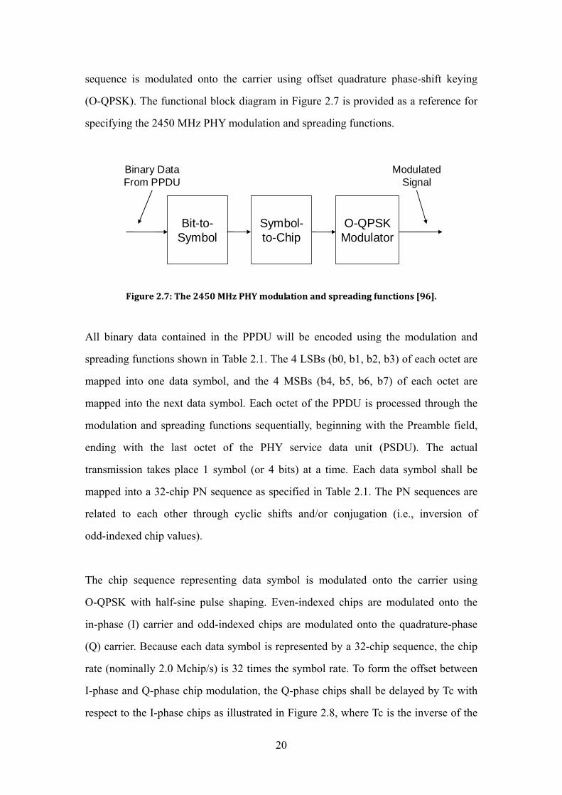
20
sequence is modulated onto the carrier using offset quadrature phase-shift keying
(O-QPSK). The functional block diagram in Figure 2.7 is provided as a reference for
specifying the 2450 MHz PHY modulation and spreading functions.
O-QPSK Modulator
Bit-to-Symbol
Binary Data From PPDU
Symbol-to-Chip
Modulated Signal
Figure 2.7: The 2450 MHz PHY modulation and spreading functions [96].
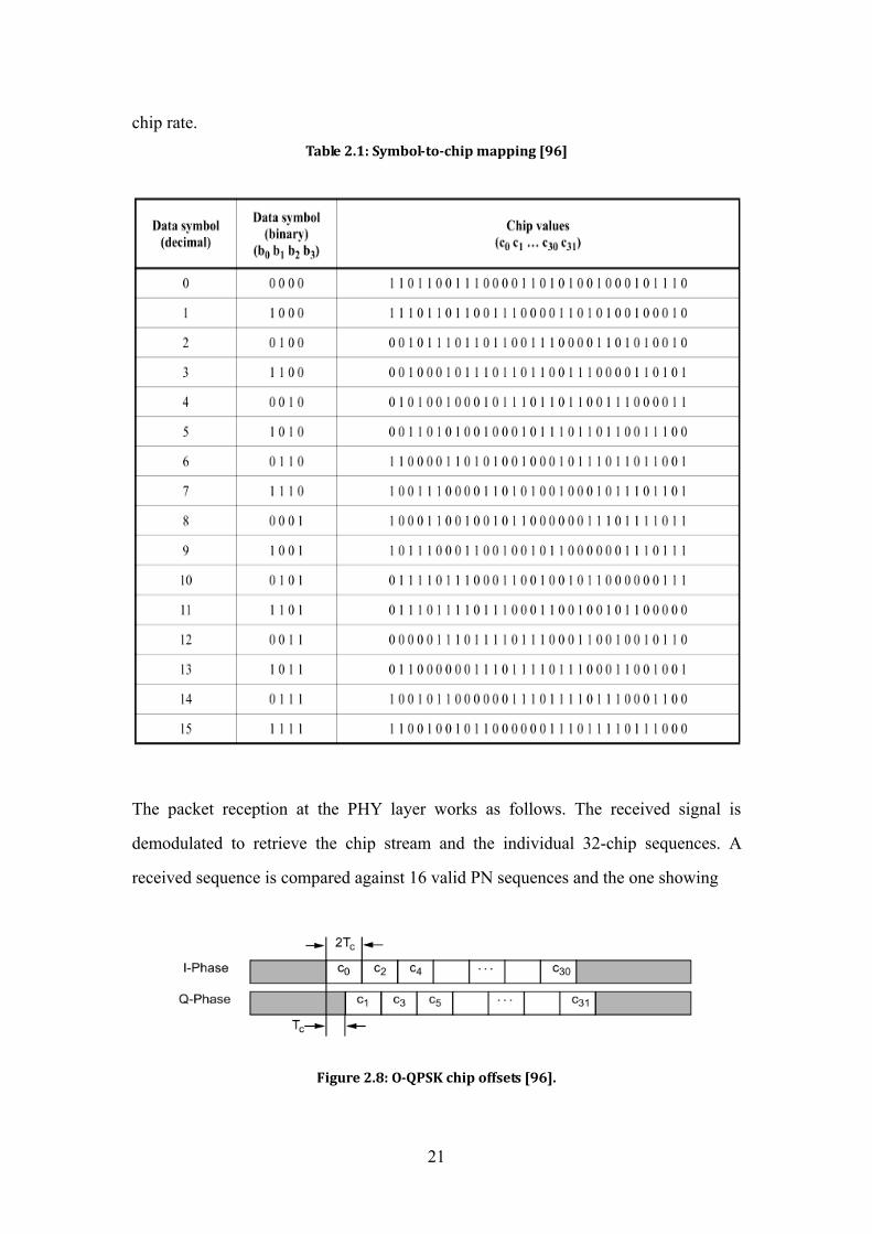
All binary data contained in the PPDU will be encoded using the modulation and
spreading functions shown in Table 2.1. The 4 LSBs (b0, b1, b2, b3) of each octet are
mapped into one data symbol, and the 4 MSBs (b4, b5, b6, b7) of each octet are
mapped into the next data symbol. Each octet of the PPDU is processed through the
modulation and spreading functions sequentially, beginning with the Preamble field,
ending with the last octet of the PHY service data unit (PSDU). The actual
transmission takes place 1 symbol (or 4 bits) at a time. Each data symbol shall be
mapped into a 32-chip PN sequence as specified in Table 2.1. The PN sequences are
related to each other through cyclic shifts and/or conjugation (i.e., inversion of
odd-indexed chip values).
The chip sequence representing data symbol is modulated onto the carrier using
O-QPSK with half-sine pulse shaping. Even-indexed chips are modulated onto the
in-phase (I) carrier and odd-indexed chips are modulated onto the quadrature-phase
(Q) carrier. Because each data symbol is represented by a 32-chip sequence, the chip
rate (nominally 2.0 Mchip/s) is 32 times the symbol rate. To form the offset between
I-phase and Q-phase chip modulation, the Q-phase chips shall be delayed by Tc with
respect to the I-phase chips as illustrated in Figure 2.8, where Tc is the inverse of the
21
chip rate. Table 2.1: Symbol-to-chip mapping [96]
The packet reception at the PHY layer works as follows. The received signal is
demodulated to retrieve the chip stream and the individual 32-chip sequences. A
received sequence is compared against 16 valid PN sequences and the one showing
Figure 2.8: O-QPSK chip offsets [96].

22
the smallest hamming distance from the received sequence is chosen as the
transmitted sequence and is translated back to the corresponding symbol. Here, the
hamming distance refers to the number of chip positions the two chip sequences differ.
Thus, a transmitted symbol will be correctly identified as long as the hamming
distance between the received sequence and the transmitted sequence is smaller than
the hamming distance between the received sequence and any other valid sequence.
Any error in identifying the transmitted symbols is likely to be identified when the
packet checksum is calculated and compared with the checksum carried in the
packet's header.
23
Chapter 3 3D IC Design Methodology
3.1 Traditional Mixed-Signal IC Design Flow
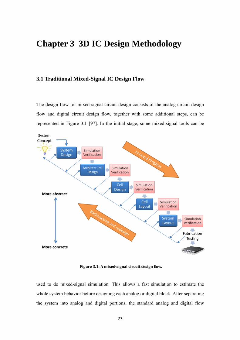
The design flow for mixed-signal circuit design consists of the analog circuit design
flow and digital circuit design flow, together with some additional steps, can be
represented in Figure 3.1 [97]. In the initial stage, some mixed-signal tools can be
used to do mixed-signal simulation. This allows a fast simulation to estimate the
whole system behavior before designing each analog or digital block. After separating
the system into analog and digital portions, the standard analog and digital flow
System Concept
System Design
Simulation Verification
Architectural Design
Cell Design
Cell Layout
System Layout
Fabrication Testing
Simulation Verification
Simulation Verification
Simulation Verification
Simulation Verification
More abstract
More concrete
Figure 3.1: A mixed-signal circuit design flow.
24
begins.
Typically, the whole 2D chip design is a collective effort by digital designers
responsible for the digital circuits and by the analog designers who are in charge of
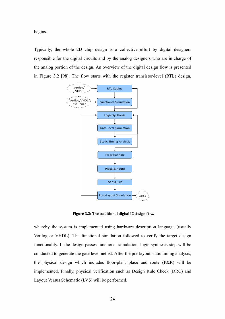
the analog portion of the design. An overview of the digital design flow is presented
in Figure 3.2 [98]. The flow starts with the register transistor-level (RTL) design,
whereby the system is implemented using hardware description language (usually
Verilog or VHDL). The functional simulation followed to verify the target design
functionality. If the design passes functional simulation, logic synthesis step will be
conducted to generate the gate level netlist. After the pre-layout static timing analysis,
the physical design which includes floor-plan, place and route (P&R) will be
implemented. Finally, physical verification such as Design Rule Check (DRC) and
Layout Versus Schematic (LVS) will be performed.
RTL Coding
Functional Simulation
Logic Synthesis
Place & Route
Post-Layout Simulation
Gate-level Simulation
Static Timing Analysis
Floorplanning
GDS2
Verilog/VHDL
Verilog/VHDLTest Bench
DRC & LVS
Figure 3.2: The traditional digital IC design flow.

25
There is a package design team as well. In the 2D IC design world, different groups
work almost independently upon the establishment of the system structure. At the end
of each flow, both the analog and digital layouts will be integrated on the same
platform, through the Cadence Virtuoso layout editor, for example. Full chip DRC,
LVS and RC extraction are then conducted. After successful execution of every step,
the final chip is ready to be sent for tape out.
3.2 3D IC Design Flow
Traditional 2D IC design flow is widely accepted and has been successfully used for
many years. An example of a high-level view of the 3D IC flow is illustrated in Figure
3.3 [99]. If the design methodology will be transferred from 2D IC to 3D IC, many
Figure 3.3: An example of a high-level view of the 3D IC design flow [99].

26
steps in the design flow may still remain. The main difference is that the design has to
be partitioned into the different available silicon layers and the back-end design needs
to be modified accordingly such as the 3D floor-plan, 3D placement and routing, 3D
RC extraction, 3D design rule check (DRC), and lastly, the layout versus schematic
(LVS) verification. Thus, most of the researchers focus on the physical design of the
whole design flow, although different aspects of the 3D IC design flow have also been
investigated.
As is illustrated in Figure 3.3, different aspects of the 3D physical design flow such as
the 3D floor-plan, 3D placement and routing, 3D RC extraction, 3D DRC, and LVS
are inducted, while the front-end design remains the same as the traditional 2D design.
However, in order to make full use of all benefits of 3D design in a mixed-signal
design, significant effort is required first at the front-end design. The front-end design
methodologies and the necessary differences between 3D ICs and traditional
mixed-signal ICs are therefore studied in this project.
3.2.1 Design Flow Impact of 3D Integration
One of the key advantages and differences the 3D integration provides is the ability to
integrate disparate fabrication technologies without disrupting the existing process
flows. As demonstrated in Figure 3.4, a device layer that is optimized for Radio
Figure 3.4: A 3D IC integrated disparate fabrication technologies [100].
Frequency (RF) circuits can be combined with another device layer that is optimized
for logic, yielding optimal system performance. By fabricating the analog and digital

27
systems on separate substrates while communicating the through high-density vias
isolation can almost be achieved.
Another difference between 3D ICs and traditional 2D ICs is the use of Through
Silicon Via (TSV) in 3D stacking. In 3D ICs, some global interconnects are now
implemented use TSV which going between stacked dies. This can result in the
reduction of the total wire length, and provides possibility for metal layer reduction
for each die. On the other hand, because the silicon area where TSV punch through
may not be utilized for building devices or 2D metal layer connections, 3D stacking
with TSV may increase the total die area of chip. Based on the TSV technologies used
in the design discussed in this thesis, the diameter of each TSV is 40 μm and the pitch
between must be at least 120 μm, as shown in Figure 3.5. Since the increased die area
will be largely determined by the achievable TSV pitch and the number of TSV used,
the optimization of the TSV number is necessary for arriving at the ultimate design.
Core
40
120
5050120
TSVMargin for Dicing
Figure 3.5: An example of TSV structure.
28
3.2.2 3D Mixed-Signal IC Design Flow
After examining the impact of 3D integration technology at the front-end design flow,
it can be seen that the two major impacts in the front-end design are the choices of the
fabrication technology, and the optimization of the TSV numbers.
As discussed in Section 3.1, the system is partitioning into analog and digital blocks
after a fast mixed-signal simulation. After the system-level partitioning, the
specifications of the various blocks that compose the design are defined, and all
digital blocks will be described in an appropriate hardware description language (e.g.,
VHDL and Verilog). For the analog blocks, it is the detailed implementation of the
different blocks of the given specifications in the selected technology process. It
results in a fully sized device-level circuit schematic. So the choice of fabrication
technologies for different dies must be made before the system-level partitioning.
That is, the system exploration and specification stage.
Different from the choice of the fabrication technologies, TSV number optimization is
not considered in just one stage but throughout the whole design flow. For the digital
block design in a mixed-signal system, both the TSV number optimizations can be
conducted through block repartitioning. Because different processes may be used for
different portions, block repartitioning shall be made just after the system-level
partitioning.
From the discussion above, it can be observed that the 3D architecture must be
considered right from the start of the design flow. The digital and analog design
groups must work together and their tools must also be coordinated. So optimizations
have to cross boundaries to achieve the best performance at the lowest power. One of

29
our research objectives is to explore the solution to address design methodology
challenges faced by 3D IC. An overview of the design flow used in this work is
illustrated in Figure 3.6.
Mixed signal modelling & simulation
Process A
Full chip integration
Full chip DRC & LVS
Full chip simulationGDSII for tape out gds2
System Specification
Analog ModuleSpecification
Digital ModuleSpecification
Analog ModuleSpecification
Digital ModuleSpecification
Analog ModuleSpecification
Digital ModuleSpecification
2D AnalogDesign Flow
2D DigitalDesign Flow
2D AnalogDesign Flow
2D DigitalDesign Flow
2D AnalogDesign Flow
2D DigitalDesign Flow
Factors:ProcessFunctionality
Factors:Number of IOPower & Area
Process B Process C
Factors:ProcessPerformancePower & AreaThermal Issues
Figure 3.6: An overview of the design flow used in this work.
The first step of the proposed 3D IC design flow remains the same as the 2D IC
design flow. That is, the system-level design exploration and specification. This is
where the system cost, performance, and power are analyzed based on estimates. One
of the factors that must be taken into account is the decision on best technology for
different dies. The choice of fabrication technologies is already important in 2D
system design and hence, even more so in the 3D system design, particularly when
multiple dies are assembled into 3D stack.
Once the process is decided, the next step is to partition the system into different
process technologies in order to optimize the design. For each process, the design is

30
divided into analog and digital portion using functional blocks so that 2D IC design
flow can be employed to different portions. At the system design level, the main
sections of the system are illustrated with block diagrams. There is no detail on the
contents of the blocks. Only the input and output characteristics of the sections are
detailed.
In the traditional 2D IC design flow, the standard analog and digital flow begins after
the system is divided into analog and digital portions. But as mentioned before, one
issue that is unique to digital core-planning in 3D ICs is to deal with the interconnects
between the different layers. In a traditional 2D IC digital core-plan, the number of
interconnects between digital core and other RF and analog blocks is not a major issue
during the core planning process. However, changes in interconnects number can have
a major impact on the area of 3D IC system. So the block repartitioning is conducted
during digital module specification. The purpose of the step is to partition the digital
core into multiple design process in order to achieve minimum area.
After the partitioning and in order to make full use of the existing design flow, the
remaining design flow is the same as the 2D IC design flow. Again the digital
designers are responsible for the digital design while analog designers are responsible
for the analog portion of the IC design. The digital system is described in RTL code
and implemented using HDL for each layer. The functional simulation is then
conducted to verify the target design functionality. This is followed by synthesizing
with the required timing constraints to get a standard cell netlist. At the end of each
design flow, the analog layout and digital layout will be integrated to form a 3D IC.
The whole system is separated into different layers according to the functionality,
process, chip area, power, cost and other design factors. Finally, the layers stack order
is analyzed with consideration of the design constrain of each module.
Once the 3D architecture of the system is decided, the next step is to optimize the
design across the multiple dies in the stack. This step presents floor-planning tools

31
with new challenges beyond the 2D realm. Different issues such as routing lengths,
electrical and thermal characteristics shall be considered at this step. Full chip DRC,
LVS and RC extraction are then performed. After every step has been executed
successfully, the final chip is ready to be sent for tape out. These sorts of new issues
become critical with 3D design. But as this research focus on front-end design, the
physical design portion is not discussed in detail.
32
Chapter 4 3D Wireless Sensor Node
One of the objectives of this research is to develop a miniaturized wireless sensor
design for patient monitoring applications. The wireless sensor node must be very
small so that the patients will not feel them and that their daily life is not affected.
Thus, the physical size of the sensor is one of the major challenges in wireless sensor
node design.
One advantage of 3D ICs is the reduction of chip area. As described in the proposed
3D IC design flow the architectural exploration and hardware partitioning will be
conducted, in order to determine and refine the optimal 3D implementation of the
system. However, till now there is no estimation tool and methodology with the
capability of comparing several implementations to allow the designer to ensure the
right calibrations and converge toward the optimal 3D implementation based on
merits such as area, power, performance and cost.
Therefore, in this research the wireless sensor node followed a traditional 2D IC
design flow at first. Then the traditional 2D wireless sensor node is repartitioned into
a 3D topology. Adopting 3D IC techniques in the design of wireless sensor node, the
3D wireless sensor node has been designed and this is one of the major contributions
of the thesis.
4.1 Wireless Sensor Node System Architecture
The architecture and hardware of the wireless sensor node are discussed in this
section. Figure 4.1 shows a system level view of the overall node architecture for
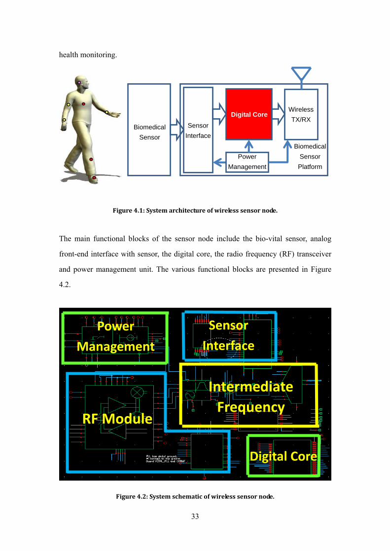
33
health monitoring.
Figure 4.1: System architecture of wireless sensor node.
The main functional blocks of the sensor node include the bio-vital sensor, analog
front-end interface with sensor, the digital core, the radio frequency (RF) transceiver
and power management unit. The various functional blocks are presented in Figure
4.2.
Figure 4.2: System schematic of wireless sensor node.
Sensor Interface
RF Module
Intermediate Frequency
Power Management
Digital Core
Power Management
BiomedicalSensor
Sensor Interface
Digital Core
Wireless TX/RX
Biomedical Sensor Platform

34
The system to be designed is separated into five portions according to the
functionality. They are the sensor interface, digital core, RF transceiver, intermediate
frequency (IF) unit and power management (PM). The analog front-end is controlled
by a microcontroller in digital core, while the RF transceiver is also interfaced with a
controller in digital core. To enable interface with RF transceivers and digital core, a
digital serial peripheral interface (SPI) and a state machine control scheme are
integrated in digital core block. The subsystems of wireless sensor node are explained
in the following sub-sections.
4.1.1 Sensing Subsystem
The sensing subsystem includes combination of biomedical sensors or monitoring
devices that are interface with sensor nodes. In this project, the blood pressure sensor
chosen is from Honeywell. A blood pressure acquisition PCB board is used to
configure the sensor. Figure 4.3 illustrates the blood pressure sensor and the
acquisition board with different passive components (R, C).
Figure 4.3: Blood pressure sensor acquisition designs.
Socket
R
BP
Sensor C
Peripheral circuits
for BP sensor
C
Small BP Sensor Acquisition Board
3D IC
R
C
C Connector
Blood Pressure Acquisition PCBMiniaturized 3D IC PCB

35
4.1.2 Analog Front-End Interface
The analog front-end interface receives, amplifies, and filters signals from the sensor.
The signal will finally be converted into the 8-bit digital data by the analog-to-digital
converter (ADC). The input signal for the analog front-end block is also the input for
the entire wireless sensor node system.
4.1.3 Communication Subsystem
A 2.45 GHz IEEE 802.15.4 standard [96] compliant RF transceiver is used as the
communication module. It is a low cost solution specially designed for low-power and
low-voltage wireless applications. The communication protocol is compatible with
IEEE 802.15.4 standard specifications.
4.1.4 Power Management Subsystem
The power management unit consists of a DC-to-DC converter for generating a 3 V
supply to low dropout regulator (LDO), and the LDO generates the supply voltages
required by analog front-end, digital core and transmission circuits. A multiple-output
LDO and a hysteresis voltage controller based DC/DC converter have been designed
in the PM unit of this work. The DC/DC converter is designed to operate with
cell-type Li-Ion battery, which has nominal voltage of 3V but up to 3.5V at its early
stage of life and down to 2.5V at its end of life. The regulator of PM units includes a
bandgap reference, one Low-Dropout Regulator (LDO) which has 0.2V voltage
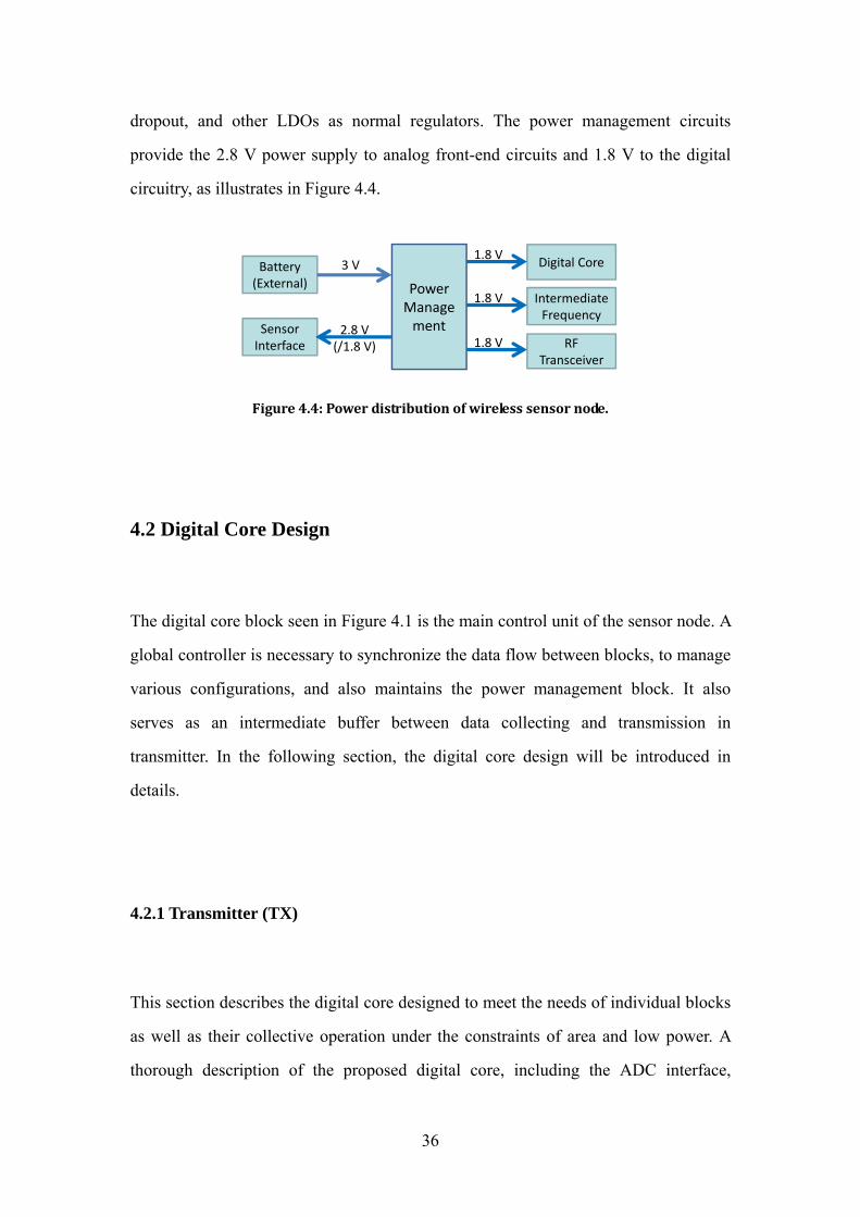
36
dropout, and other LDOs as normal regulators. The power management circuits
provide the 2.8 V power supply to analog front-end circuits and 1.8 V to the digital
circuitry, as illustrates in Figure 4.4.
Power Manage
ment
Digital Core
Intermediate Frequency
RF Transceiver
Sensor Interface
Battery (External)
3 V
2.8 V (/1.8 V)
1.8 V
1.8 V
1.8 V
Figure 4.4: Power distribution of wireless sensor node.
4.2 Digital Core Design
The digital core block seen in Figure 4.1 is the main control unit of the sensor node. A
global controller is necessary to synchronize the data flow between blocks, to manage
various configurations, and also maintains the power management block. It also
serves as an intermediate buffer between data collecting and transmission in
transmitter. In the following section, the digital core design will be introduced in
details.
4.2.1 Transmitter (TX)
This section describes the digital core designed to meet the needs of individual blocks
as well as their collective operation under the constraints of area and low power. A
thorough description of the proposed digital core, including the ADC interface,

37
microcontroller (MCU), serial peripheral interface, memory and parts of the RF
transceivers is provided in this sub-section. The IEEE 802.15.4 Standard compliant
digital core design at the transmitter section of the design is shown in Figure 4.5.
ADC Interface
ADC_SCLK
ADC_CSN
ADC_DATA
Micro Controller
SPI Interface
Status & Control
Registers
TXFIFO
TX Data & CRC
Preamble Generator
ID Generator
To internal RF&Analog
Block
Figure 4.5: Transmitter digital core block diagram.
The ADC interface functions as an interface between the ADC and digital core to
provide the necessary signal to ADC. The memory blocks which store temporary data
and intermediate results have been partitioned based on different access patterns. The
controller manages timing and data flow among the blocks. Finally signals from
sensor are then formatted into packets for wireless transmission and sent to the
transceiver. The whole function of the digital core was designed in Verilog code and
initially tested individually in SimVision to verify its operation prior to system
integration. The verification is done through FPGA implementation. The sub-blocks
of the digital core are explained in the following sub-sections.

38
4.2.1.1 Analog Front-End Interface
The operation of the front-end ADC is controlled by a state machine based
microcontroller, which depending upon the runtime configuration settings, allows the
flexibility for recording. The controller multiplexes the channels before the data is
handed over to processor. The ADC interface to the microcontroller is an 8-bit shift
register. The ADC interface is also responsible for providing the appropriate clock to
the ADC. The serial interface timing diagram for the ADC is shown in Figure 4.6. The
chip select signal is CSN, which initiates conversions on the ADC and frames the
serial data transfers. SCLK (serial clock) controls both the conversion process and the
timing of serial data. The serial data out pin is SDATA, where a conversion result is
found as a serial data stream.
Figure 4.6: ADC timing diagram.
Basic operation of the ADC starts with CSN going low, which initiates a conversion
process and data transfer. With reference to the falling edge of CSN, subsequent rising
and falling edges of SCLK will be labeled; for instance, "the fourth falling edge of
SCLK" shall refer to the fourth falling edge of SCLK after CSN goes low. The input
signal is sampled and held for conversion on the falling edge of CSN.
In order to read a complete sample from the ADC, 16 SCLK cycles are required. The
1 MHz
(Serial Output
Data Rate)
ADC DATA
1 kHz
(Sampling
Rate)

39
sample bits (including leading or trailing zeroes) are clocked out on falling edges of
SCLK. They are intended to be clocked in by a receiver on subsequent rising edges of
SCLK. Three leading zero bits on SDATA will be produced by the ADC, followed by
eight data bits, most significant first. After the data bits, the ADC will clock out four
trailing zeros.
4.2.1.2 FIFO
The FIFO can be used to improve the processing ability of the digital core. In this
design, single-port SRAM is used as FIFO for the main memory instead of shift
registers. Since the chip area is the main concern in this design, a 64-byte FIFO is
used as the interface between the microcontroller and digital packet encoder. The
transmitting data is first written into the FIFO. The single-port SRAM has one read
port and one write port. The two ports are independent. In this case, the write port is
connected to the ADC interface and the read port is connected to the packet encoder
This means only the packet generator can read the data ADC interface has written to
the FIFO. Figure 4.7 shows the internal structure of two of the FIFOs.
1kbps
1 bitADC
Memory 1
D7 D6 D5 D4 D3 D2 D1 D0
Bits for 1 sample
250kbps
1 bit
TX Encoder
Memory 2
D7 D6 D5 D4 D3 D2 D1 D0
D7 D6 D5 D4 D3 D2 D1 D0 D7 D6 D5 D4 D3 D2 D1 D0
D7 D6 D5 D4 D3 D2 D1 D0
D7 D6 D5 D4 D3 D2 D1 D0
Figure 4.7: The internal structure of two of the FIFOs.
As illustrated in Figure 4.7, this FIFO has capacity for two packets, each up to 18
bytes in length. The two FIFOs are alternately transmitted, so the ADC interface can
be filling one while the other is transmitting. As is the case with the standard cell
40
libraries, the layouts view of the memory is not available. Instead, Verilog model
include the simulation data such as bus width, memory size is used.
4.2.1.3 ID Generator
The identity (ID) generator module is used to generate the ID byte for the associated
data packet. The generated ID byte will be appended after the packet length byte when
transmitting. The main functional block in ID generator is the counter. As the
transmitter will send more repetitions of each packet, the ID byte is used to
distinguish different packets. In the receiver modules the ID byte is checked against
the previous ID byte of the receiver and the data is not saved unless they are the
different.
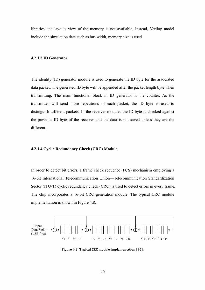
4.2.1.4 Cyclic Redundancy Check (CRC) Module
In order to detect bit errors, a frame check sequence (FCS) mechanism employing a
16-bit International Telecommunication Union—Telecommunication Standardization
Sector (ITU-T) cyclic redundancy check (CRC) is used to detect errors in every frame.
The chip incorporates a 16-bit CRC generation module. The typical CRC module
implementation is shown in Figure 4.8.
Figure 4.8: Typical CRC module implementation [96].

41
The CRC module is used to generate the CRC bits for the associated data packet. The
CRC generation core is a large XOR tree which processes 1 bit of data each cycle.
The initial state of the CRC module can be set to an arbitrary value. The CRC
polynomial is given by
1)( 51216 +++= xxxxG (4.1)
The transmitter modules generate the CRC bits and append them to the end of the
packet when transmitting, while the receiver modules compute the CRC over the
entire packet, including the CRC bits, and then check that the data in the CRC
generator is all zeros which indicate the CRC is correct. Before transmission or
reception, the CRC is cleared.
4.2.1.5 Packet Generator
The transmitting data stream from the information source is first fed through a simple
packet generator. The packet generator is responsible for placing the synchronization
header on the packet, reading from the data buffer and sending the packet. The
payload data from the data buffer is prefixed with a synchronization header (SHR),
containing the preamble sequence and Start-of-Frame Delimiter (SFD) fields, and a
PHY header (PHR) containing the length of the PHY payload in octets. It also
appends the CRC to the packet. The SHR, PHR, and PHY payload with CRC bytes
together form the PHY packet (i.e., PPDU). Then physical layer protocol data unit
(PPDU) packet will be modulated by a low power modulator, and transmitted by RF
module.
The packet generator module in the transmitter contains an ID generator, a CRC
42
generator, a packet encoder. The design tradeoffs for the packet generator design were
focused on simplicity and improving probability of successful delivery. Since the
transmitter is compatible with IEEE 802.15.4 standards, the designed data rate is 250
kb/s. The transmitter operates at 2.45 GHz which is in the ISM band. The design of
the packet generator system follows a low complexity low power PHY specification.
The structure of the physical layer protocol data unit (PPDU) packet is illustrated in
Figure 4.9.
Figure 4.9: Format of the PPDU.
The synchronization header has two fields. The first field is the preamble sequence
field, which is used by the packet detection circuitry to confirm a packet is present.
The length of the preamble is 4 bytes. The first preamble field consists of repeating
binary zeros. The second field is the Start-of-Frame Delimiter (SFD) field, which
allows the receiver to get an absolute position of the start of the packet. The length of
the SFD is 8-bit and shall be formatted as illustrated in Figure 4.10.
Figure 4.10: Format of the SFD field [96].
The frame length field is of 7 bits and it specifies the total number of octets contained
in the payload. The permitted length of the payload data within one packet should be
no more than 127 octets. The first byte written to the packet buffer is the length of the
packet, including the CRC and the ID byte, but excluding the length byte.
Data in frame
ID (1 Byte)
Frame Length (7 Bits)
SFD (1 Byte)
Preamble (4 Bytes)
SHR (5 Bytes) PHR (1 Byte)
Reserved (1 Bit)
PHY payload
CRC (2 Bytes)
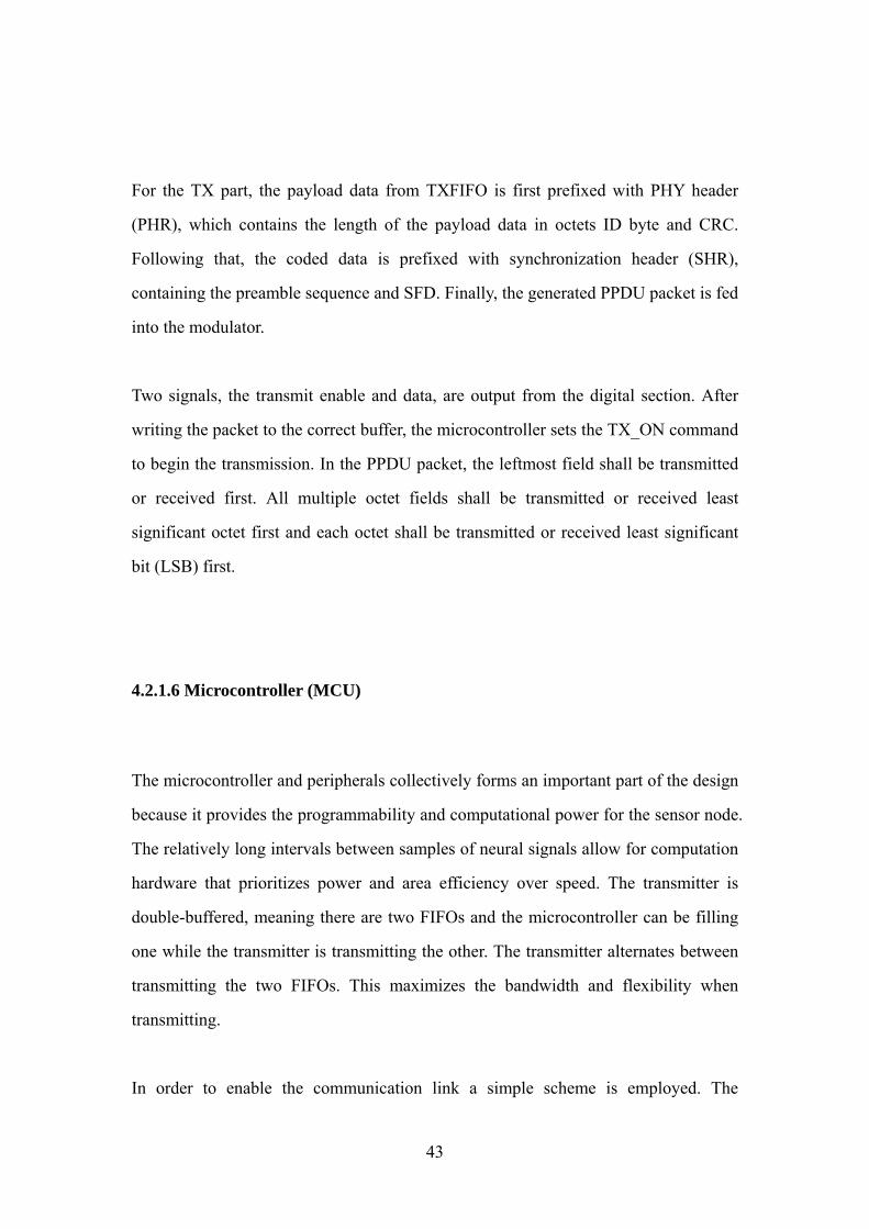
43
For the TX part, the payload data from TXFIFO is first prefixed with PHY header
(PHR), which contains the length of the payload data in octets ID byte and CRC.
Following that, the coded data is prefixed with synchronization header (SHR),
containing the preamble sequence and SFD. Finally, the generated PPDU packet is fed
into the modulator.
Two signals, the transmit enable and data, are output from the digital section. After
writing the packet to the correct buffer, the microcontroller sets the TX_ON command
to begin the transmission. In the PPDU packet, the leftmost field shall be transmitted
or received first. All multiple octet fields shall be transmitted or received least
significant octet first and each octet shall be transmitted or received least significant
bit (LSB) first.
4.2.1.6 Microcontroller (MCU)
The microcontroller and peripherals collectively forms an important part of the design
because it provides the programmability and computational power for the sensor node.
The relatively long intervals between samples of neural signals allow for computation
hardware that prioritizes power and area efficiency over speed. The transmitter is
double-buffered, meaning there are two FIFOs and the microcontroller can be filling
one while the transmitter is transmitting the other. The transmitter alternates between
transmitting the two FIFOs. This maximizes the bandwidth and flexibility when
transmitting.
In order to enable the communication link a simple scheme is employed. The

44
transmitter may send more repetitions of each packet. This is recommended because
the probability that the packet detection circuitry successfully detects the packet will
be increased. Since the first preamble consists of many repetitions of a short code,
once the packet detection circuitry recognizes the start of packet preamble, it is not
able to know absolutely where the beginning of the packet is. This is the job of the
second preamble. When a packet is detected by the packet detection circuitry, the
digital control disables the packet detection circuitry and the symbol synchronization
and bit detection circuitry are enabled. Once the packet detection circuit detects a
packet, in order to determine the start of the packet, the bit detection circuit correlates
its output with the expected PN code found in the second preamble. The second
preamble is also responsible for identifying false alarms caused by the packet detect
logic. The overall false packet detection rate is very low because of the long PN code
in the second preamble.
After the first two preambles, there is the packet length and the ID bytes. The ID byte
is checked against the previous ID byte of the receiver and is not saved unless they are
different. The packet length is the length of the data payload, the CRC and ID byte,
but not the length byte. The maximum data payload size is then set to 18 bytes. The
ID and length bytes are arguably more important than the rest of the payload, because
an error in those bytes can cause problems in the receiver. For example, an error in the
length byte could direct the receiver to receive a very long packet which is not present,
thereby stopping the receiver from hearing a retry of the same packet. For this reason,
send more repetition of each packet scheme is employed. This gives extra assurance
that these bytes will be received correctly. After the data payload, a 16-bit CRC is
present. This is automatically generated and checked by CRC module. As shown in
Figure 4.5, microcontroller block controls the packet generation in transmit state. The
controller consists of a large mealy finite state machine and the instruction register. In
this design, the control section is a 14-state state machine, as shown in Figure 4.11.
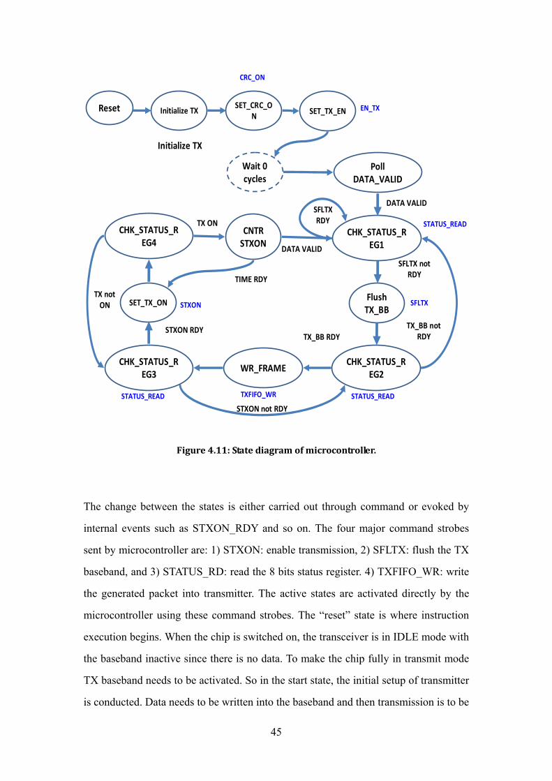
45
Reset SET_TX_EN
Wait 0 cycles
Poll DATA_VALID
CHK_STATUS_REG1
WR_FRAME
Initialize TX
STATUS_READ
TXFIFO_WR
Initialize TX SET_CRC_ON
CHK_STATUS_REG3
STXON RDY
EN_TX
DATA VALID
CRC_ON
CHK_STATUS_REG2
Flush TX_BB
SFLTX not RDY
SFLTX RDY
SFLTX
TX_BB RDYTX_BB not
RDY
STATUS_READSTATUS_READSTXON not RDY
SET_TX_ON
CHK_STATUS_REG4
CNTR STXON
TX ON
STXONTX not
ON
TIME RDY
DATA VALID
Figure 4.11: State diagram of microcontroller.
The change between the states is either carried out through command or evoked by
internal events such as STXON_RDY and so on. The four major command strobes
sent by microcontroller are: 1) STXON: enable transmission, 2) SFLTX: flush the TX
baseband, and 3) STATUS_RD: read the 8 bits status register. 4) TXFIFO_WR: write
the generated packet into transmitter. The active states are activated directly by the
microcontroller using these command strobes. The “reset” state is where instruction
execution begins. When the chip is switched on, the transceiver is in IDLE mode with
the baseband inactive since there is no data. To make the chip fully in transmit mode
TX baseband needs to be activated. So in the start state, the initial setup of transmitter
is conducted. Data needs to be written into the baseband and then transmission is to be
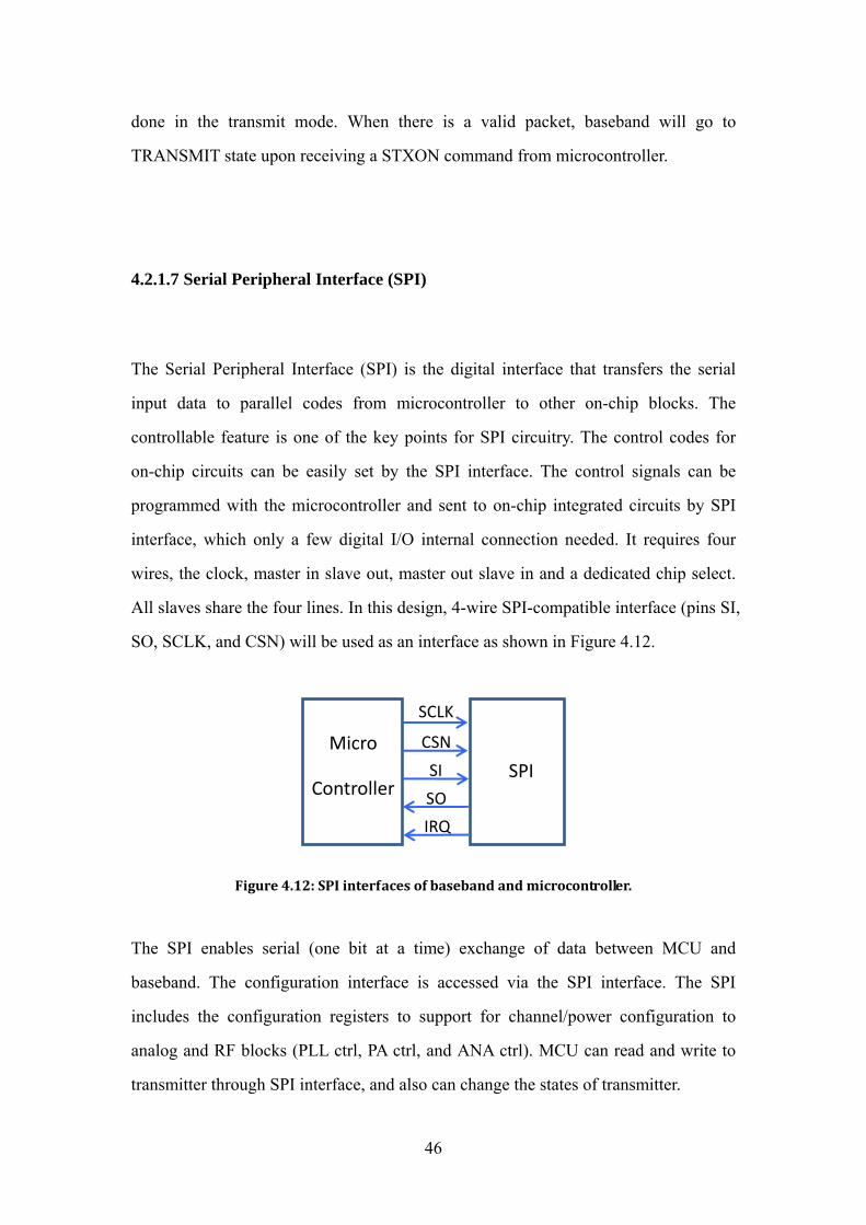
46
done in the transmit mode. When there is a valid packet, baseband will go to
TRANSMIT state upon receiving a STXON command from microcontroller.
4.2.1.7 Serial Peripheral Interface (SPI)
The Serial Peripheral Interface (SPI) is the digital interface that transfers the serial
input data to parallel codes from microcontroller to other on-chip blocks. The
controllable feature is one of the key points for SPI circuitry. The control codes for
on-chip circuits can be easily set by the SPI interface. The control signals can be
programmed with the microcontroller and sent to on-chip integrated circuits by SPI
interface, which only a few digital I/O internal connection needed. It requires four
wires, the clock, master in slave out, master out slave in and a dedicated chip select.
All slaves share the four lines. In this design, 4-wire SPI-compatible interface (pins SI,
SO, SCLK, and CSN) will be used as an interface as shown in Figure 4.12.
Figure 4.12: SPI interfaces of baseband and microcontroller.
The SPI enables serial (one bit at a time) exchange of data between MCU and
baseband. The configuration interface is accessed via the SPI interface. The SPI
includes the configuration registers to support for channel/power configuration to
analog and RF blocks (PLL ctrl, PA ctrl, and ANA ctrl). MCU can read and write to
transmitter through SPI interface, and also can change the states of transmitter.
SCLK
CSNMicro
Controller SPI SI
SOIRQ
47
The microcontroller interface uses 4 pins for the SPI configuration interface (SI, SO,
SCLK and CS_N). SPI also has an interrupt pin (IRQ) to MCU. The IRQ will notify
the MCU, for instance, transmission is completed and payload has been saved in the
TXFIFO successfully and so on. The operation of SPI command is illustrated in
Figure 4.13.
The SPI clock (SCLK) provided by MCU is 1 MHz. SO pin is used as the data output
from SPI. SI, SCLK and CSN (chip select, active low) pins are the outputs of MCU.
Figure 4.13: Illustration of SPI command timing waveform.

48
Hence, SO should be connected to an input port of the microcontroller. SI, SCLK and
CSN must be microcontroller outputs. The CSN (chip select) is an active low signal,
which means that baseband will only process the data from SI when CSN is low. The
CSN must be low before the first rising edge of the SPI clock. Baseband SPI will
sample the data on SI at the positive edge of SCLK and the data on SO will be
updated at the positive edge of SCLK. The SI and SO always follow the LSB first.
The first byte of each MCU command will be treated as command code, then if may
be followed by the data bytes. All command and data byte will be transmitted the
most significant bit first. Multiple commands per SPI session is supported but only
one TXFIFO_WRITE or RXFIFO_READ is allowed, and they must be the last
command per SPI session. This can enable transmitter to detect the
overflow/underflow condition of these two commands.
4.2.2 Receiver (RX)
The design constraint of the digital core at the receiver part is not as strict as that of
the transmitter since the chip area is not the main concern in this design. An IEEE
802.15.4 Standard compliant transceiver is employed. The transceiver operates at 2.45
GHz which is in the ISM band. The receiver is compatible with the transmitter. It
shares a similar architecture with the transmitter.
The receive process begins with the antenna output connected to a 2.45 GHz RF front
end. The front end block represents the typical receive components of a 2.45 GHz
band pass filter, low noise amplifier and variable gain amplifier with gain control.
Next, the signal is down-converted to the IF frequency. Then the signal is digitized
and passed through the same filter that was used in the transmitter. The filter output is

49
down-sampled. For the receiver part, the input of the baseband is the demodulated
binary signals from demodulator.
The signals are first fed into the synchronizer block in order to achieve bit and packet
synchronization. The synchronization is achieved by detecting peaks of correlation
between the received signals and the local SHR sequence. The receiver detects the
two preambles which allow the receiver to get an absolute position of the start of the
packet. A preamble threshold thh_pre and a SFD threshold thh_sfd are set up,
respectively. The preamble correlation between the local preamble sequence and
received signals is first calculated. Following that, the SFD correlation between the
local SFD and received signals is calculated. After acquiring synchronization, the
preamble sequence and SFD can be removed. Following that, PHR is decoded first, in
order to obtain the length information of PSDU. During decoding, if the system
detects the errors but cannot correct them, the receiver will wait for re-transmission.
After the receiver acquires the length information of PSDU, the PSDU can be
decoded. The final received PSDU packet will be fed into microcontroller.
4.2.2.1 Digital Core
The architecture of the digital core in the receiver and the transmitter is similar. As
illustrated in Figure 4.14, the digital core includes microcontroller, CRC checker,
memory and output interface. The same as transmitter, receiver is double-buffered,
meaning there are two FIFOs and the microcontroller can be read one while the
receiver is receiving the other. A 16-bit hardware CRC checker which is used to check
the CRC for the associated data packet is integrated. The receiver modules compute
the CRC over the entire packet, including the CRC bits, and then check that the data
in the CRC generator is all zeros which indicate the CRC is correct. Also ID byte is
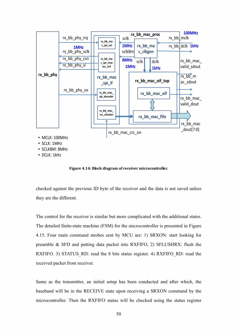
50
• MCLK: 100MHz• SCLK: 1MHz• SCLK8M: 8MHz• DCLK: 1kHz
rx_bb_mac_spi_if
rx_bb_mac_oif
rx_bb_mac_fifo
rx_bb_phy_so
rx_bb_phy_irq
rx_bb_phy_csnrx_bb_phy_si
yrx_bb_phy
rx_bb_mac_proc
rx_bb_mac_valid_dout
rx_bb_mac_clkgen
rx_bb_mac_dout[7:0]
rx_bb_phy_sclk1MHz
sclk
dclk
rx_bb_mclk100MHz
rx_bb_dclk 1kHz
rx_bb_mac_crc_checker
1kHz
1MHzrx_bb_mac_spi_sm
sclk1MHz
rx_bb_mac_spi_mas
ter_ctrl
rx_bb_mac_spi_decoder
rx_bb_mac_oif_top
sclk8m
8MHz
rx_bb_mac_crc_on
rx_bb_mac_valid_sdout
rx_bb_mac_sdout
Figure 4.14: Block diagram of receiver microcontroller.
checked against the previous ID byte of the receiver and the data is not saved unless
they are the different.
The control for the receiver is similar but more complicated with the additional states.
The detailed finite-state machine (FSM) for the microcontroller is presented in Figure
4.15. Four main command strobes sent by MCU are: 1) SRXON: start looking for
preamble & SFD and putting data packet into RXFIFO, 2) SFLUSHRX: flush the
RXFIFO. 3) STATUS_RD: read the 8 bits status register. 4) RXFIFO_RD: read the
received packet from receiver.
Same as the transmitter, an initial setup has been conducted and after which, the
baseband will be in the RECEIVE state upon receiving a SRXON command by the
microcontroller. Then the RXFIFO status will be checked using the status register

51
Reset
SET_SRXON
Wait 0 cycles
Poll IRQ
IRQ=0
CHK_STATUS_REG1
IRQ=1
Flush RXFIFO
RD_FRAME
RXFIFO RDY
Initialize RX
STATUS_READ SFLRX
RXFIFO_RD
Fractional-N-*SRXONBB_CTRL
SET_FRAC_N
SET_CRC_EN off
BPRO_RX_BB_MAC_SPI_SM
CHK_STATUS_REG2
CHK_STATUS_REG3
SRXON RDY
STATUS_READ
STATUS_READ
SFLRX not RDY
SFLRX RDY
SRXONRX_BB _IRQ:IRQ=1 assertion cases:1.Status Reg Frame_Received=1. At least one valid frame unread is stored in RXFIFO.2.The data length indicated by frame length byte does not match for the number of SCLK provided by RXFIFO_Read commandOnly cleared by STATUS_READ command
CMD_SFLRX:To clear status Regbits Frame_Received, Rxfifo_Overflow and reset Rxfifo
SFLRX_RDY:Flush will not be success when status Reg bit Receive_Complete=0, if it is 0, check status reg regularly until Receive_complete=1
SRXON_RDY:Check whether CMD_SFLRX is success. Status Reg bits Frame_Received and Rxfifo_overflow should both be 0, if not, send CMD_SFLRX again.
RXFIFO not RDY
SRXON not RDY
Figure 4.15: State diagram of microcontroller in receiver part.
read command (STATUS_RD) when interrupt register (MCU_INT) gets high. If
RXFIFO_OVERFLOW or RX_DATA_ERROR bit is high, SFLRX command will be
conducted to flush the RX data. If only FRAME_RECEIVED bit is high,
RXFIFO_RD command will be sent to let MCU read data in RXFIFO through SDO.
Finally, if the CRC check result is correct, the received data will be fed out in parallel
8 bits IO through output interface at frequency 1 kHz. In order to achieve continuous
8 bits parallel output the same 2 FIFOs structure which is used in TX part is used as
well. One FIFO for 8 bits parallel output, another for new frame receiving. If the
baseband detects error in received data and cannot correct it, or if there is overflow in
RXFIFO, the baseband will stop receiving any further packet and inform MCU by
interrupt (MCU_INT).

52
4.3 3D Architecture
This section describes the 3D architecture of the entire sensor system. 3D IC design
requires solid 3D design flow [101]. In this project, the 3D IC design flow is
developed through significant enhancements on the existing 2D design and
verification tools.
In the migration of design methodology from 2D IC to 3D IC, many steps in the
design flow remain deployable. The difference is that the design has to be partitioned
into different silicon layers available. By repartitioning functional blocks into
different layers and optimizing the order of these layers, it enables the possibility of
reducing chip area. In this project, the only process technology available is 0.18 µm.
As a result, the process technology choice issue is not considered here.
4.3.1 Design Exploration
Aligned with the 2D design flow, design exploration is the first step essential for the
3D IC design. The purpose of this step is to analyze the design carefully and arrive at
a conclusion on whether the 3D stacking will yield an advantage on the
cost/functionality/size of the circuit. The design need to be divided into different dies
that can take full advantage of the 3D concept. The partition should be 3D aware in
the sense that it should take into account the side effects that may occur due to vertical
stacking, for example the EMI between different dies, thermal effects of the stacking
[102, 103], etc. The stack order depends on the number of TSVs that a particular die
can afford because the lower dies should carry the TSVs related to input/output
signals of the upper dies. Figure 4.16 shows the design of the Wireless Transceiver
which is to be stacked in the 3D domain.
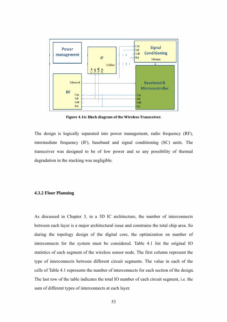
53
Figure 4.16: Block diagram of the Wireless Transceiver.
The design is logically separated into power management, radio frequency (RF),
intermediate frequency (IF), baseband and signal conditioning (SC) units. The
transceiver was designed to be of low power and so any possibility of thermal
degradation in the stacking was negligible.
4.3.2 Floor Planning
As discussed in Chapter 3, in a 3D IC architecture, the number of interconnects
between each layer is a major architectural issue and constrains the total chip area. So
during the topology design of the digital core, the optimization on number of
interconnects for the system must be considered. Table 4.1 list the original IO
statistics of each segment of the wireless sensor node. The first column represent the
type of interconnects between different circuit segments. The value in each of the
cells of Table 4.1 represents the number of interconnects for each section of the design.
The last row of the table indicates the total IO number of each circuit segment, i.e. the
sum of different types of interconnects at each layer.

54
Table 4.1: IO statistics of each portion in 3D ICs
Layer RF SC PM DIG IF SYSTEM
SC,IO 11 11
SC,IO,PM 1 1 1
SC,IO,PM,DIG,IF,RF 2 2 2 2 2 2
SC,PM 1 1
SC,DIG 15 15
SC,PM,IF 1 1 1
PM,IO 9 9
RF,IO,PM 1 1 1
IO,PM,IF,RF 1 1 1 1
PM,DIG 1 1
PM,IF 3 3
PM,RF 2 2
DIG,IO 6 6
DIG,IF 18 18
DIG,RF 35 35
IF,RF 4 4
RF,IO 8 8
TOTAL IO 53 31 22 77 29 39
As illustrated in the column of DIG in Table 4.1, the number of interconnects of the
digital portion is 77, which is far more than that of other portions. The major factors
that contribute to the large number of interconnects are mainly the number of
interconnects between the digital core and the sensor interface, RF and IF portions,
which is 15, 35 and 18 separately. Further analysis shows that the internal control
signal between digital core and sensor interface, RF and IF portions is the main issue,
which constrains the total IO number in the digital core. So in order to minimize the
total number of interconnects between each portion, the status and control register

55
block and related SPI block is repartitioned into different related portions according to
the functionality. Three blocks in total were moved from the digital core portions to
other portions, which are RF, sensor interface and inter-mediate frequency separately.
Table 4.2 shows the IO statistics result after the optimization.
As illustrated in Table 4.2, after the architecture optimization, the number of IO at
each portion became more balanced. Although digital core still contains the most
number of interconnects, the IO number was decreased from 77 to 39. More important,
Table 4.2: IO statistics of each portion in 3D ICs after digital core architecture optimization
Layer RF SC PM DIG IF SYSTEM
SC,IO 11 11
SC,IO,PM 1 1 1
SC,IO,PM,DIG,IF,RF 2 2 2 2 2 2
SC,IO,DIG,IF,RF 3 3 3 3 3
SC,DIG,IF,RF 1 1 1 1
SC,PM 1 1
SC,DIG 3 3
SC,PM,IF 1 1 1
PM,IO 9 9
RF,IO,PM 1 1 1
IO,PM,IF,RF 1 1 1 1
PM,DIG 1 1
PM,IF 3 3
PM,RF 2 2
DIG,IO 3 3
DIG,IF 13 13
DIG,RF 13 13
IF,RF 4 4
RF,IO 8 8
TOTAL IO 35 23 22 39 28 39
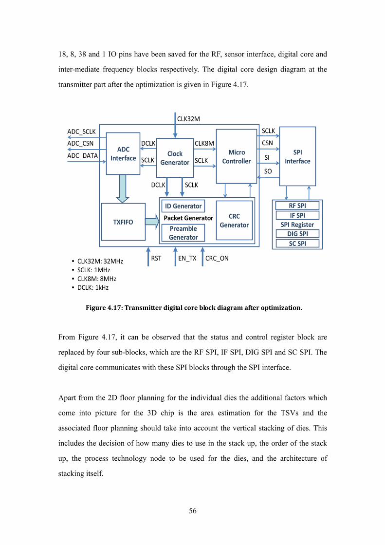
56
18, 8, 38 and 1 IO pins have been saved for the RF, sensor interface, digital core and
inter-mediate frequency blocks respectively. The digital core design diagram at the
transmitter part after the optimization is given in Figure 4.17.
From Figure 4.17, it can be observed that the status and control register block are
replaced by four sub-blocks, which are the RF SPI, IF SPI, DIG SPI and SC SPI. The
digital core communicates with these SPI blocks through the SPI interface.
Apart from the 2D floor planning for the individual dies the additional factors which
come into picture for the 3D chip is the area estimation for the TSVs and the
associated floor planning should take into account the vertical stacking of dies. This
includes the decision of how many dies to use in the stack up, the order of the stack
up, the process technology node to be used for the dies, and the architecture of
stacking itself.
Micro Controller
ADC Interface
TXFIFO
Clock Generator
DCLK
• CLK32M: 32MHz• SCLK: 1MHz• CLK8M: 8MHz• DCLK: 1kHz
DCLK
Packet Generator
CRC_ON
ADC_SCLK
ID GeneratorCRC
Generator
ADC_CSN
ADC_DATA
Preamble Generator
SPI InterfaceSCLK
CLK8M
SCLK
SCLK
CLK32M
SCLK
CSN
SI
SO
SPI Register
RF SPIIF SPI
DIG SPISC SPI
EN_TXRST
Figure 4.17: Transmitter digital core block diagram after optimization.
57
As discussed in Chapter 3, the system is separated into five portions according to the
functionality. They are the sensor interface, digital core, RF transceiver, intermediate
frequency (IF) unit and power management (PM). As this is a first attempt to use the
TSV as an interconnect technology in a 3D integration design, so in order to minimize
the design complexity, the design is logically separated into the same five dies. Once
the five dies are decided, the next step is to decide on the layers’ stack order.
Considering the compatibility for future versions and design constrains of the RF
block, the sensor die is usually placed on top of the stack while the IF and RF layers
should be at the bottom. Since the location of the sensor layer, IF and RF layer are
fixed, the only design freedom is the order of the Power Management layer and
Digital Core layer. The two stacking orders are from top to bottom and they are (1)
SC, PM, DIG, IF, RF and (2) SC, DIG, PM, IF, RF.
Since the system is separated into five dies according to their functionality, the
number of TSV used for each layer can be calculated. Table 4.3 and Table 4.4 list the
TSV statistics of each layer in different orders. The same as Table 4.1, the first row is
the type of interconnects between the different portion. The value in the following
cells is the number of TSV each portion must have for that kind of interconnects. The
final line of the table is the total TSV number of each portion which is the sum of the
column. The system column represents the whole system.
As is illustrated in Table 4.4, a total of 216 and 227 TSVs will be used with the
stacking sequence of SC, PM, DIG, IF, RF, and the stacking sequence SC, DIG, PM,
IF, RF separately. That means, with stacking sequence of SC, PM, DIG, IF, RF, 11
TSVs can be saved as compared to the sequence, SC, DIG, PM, IF, RF. In order to
save the total chip area, the stacking order SC, PM, DIG, IF, RF is used. The 3D
architecture of the wireless sensor node is provided in Figure 4.18.
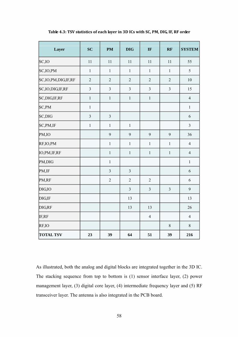
58
Table 4.3: TSV statistics of each layer in 3D ICs with SC, PM, DIG, IF, RF order
Layer SC PM DIG IF RF SYSTEM
SC,IO 11 11 11 11 11 55
SC,IO,PM 1 1 1 1 1 5
SC,IO,PM,DIG,IF,RF 2 2 2 2 2 10
SC,IO,DIG,IF,RF 3 3 3 3 3 15
SC,DIG,IF,RF 1 1 1 1 4
SC,PM 1 1
SC,DIG 3 3 6
SC,PM,IF 1 1 1 3
PM,IO 9 9 9 9 36
RF,IO,PM 1 1 1 1 4
IO,PM,IF,RF 1 1 1 1 4
PM,DIG 1 1
PM,IF 3 3 6
PM,RF 2 2 2 6
DIG,IO 3 3 3 9
DIG,IF 13 13
DIG,RF 13 13 26
IF,RF 4 4
RF,IO 8 8
TOTAL TSV 23 39 64 51 39 216
As illustrated, both the analog and digital blocks are integrated together in the 3D IC.
The stacking sequence from top to bottom is (1) sensor interface layer, (2) power
management layer, (3) digital core layer, (4) intermediate frequency layer and (5) RF
transceiver layer. The antenna is also integrated in the PCB board.
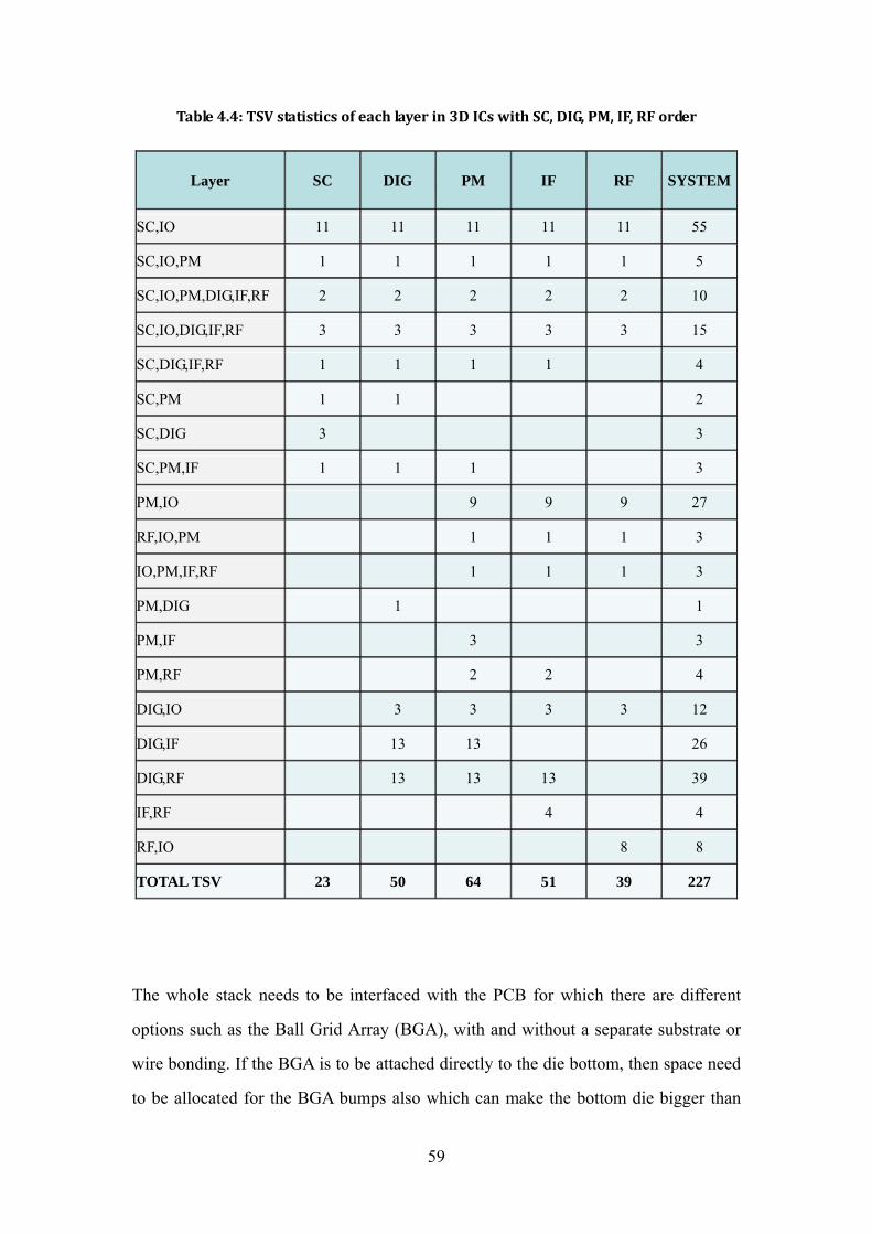
59
Table 4.4: TSV statistics of each layer in 3D ICs with SC, DIG, PM, IF, RF order
Layer SC DIG PM IF RF SYSTEM
SC,IO 11 11 11 11 11 55
SC,IO,PM 1 1 1 1 1 5
SC,IO,PM,DIG,IF,RF 2 2 2 2 2 10
SC,IO,DIG,IF,RF 3 3 3 3 3 15
SC,DIG,IF,RF 1 1 1 1 4
SC,PM 1 1 2
SC,DIG 3 3
SC,PM,IF 1 1 1 3
PM,IO 9 9 9 27
RF,IO,PM 1 1 1 3
IO,PM,IF,RF 1 1 1 3
PM,DIG 1 1
PM,IF 3 3
PM,RF 2 2 4
DIG,IO 3 3 3 3 12
DIG,IF 13 13 26
DIG,RF 13 13 13 39
IF,RF 4 4
RF,IO 8 8
TOTAL TSV 23 50 64 51 39 227
The whole stack needs to be interfaced with the PCB for which there are different
options such as the Ball Grid Array (BGA), with and without a separate substrate or
wire bonding. If the BGA is to be attached directly to the die bottom, then space need
to be allocated for the BGA bumps also which can make the bottom die bigger than
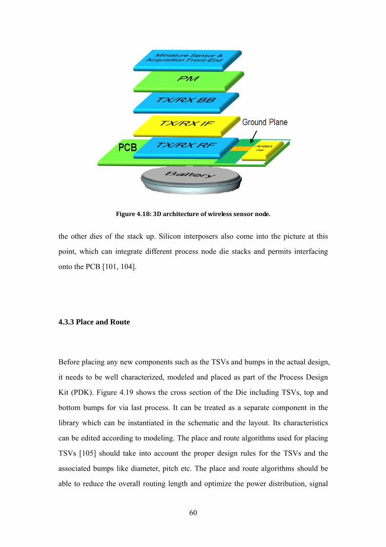
60
Figure 4.18: 3D architecture of wireless sensor node.
the other dies of the stack up. Silicon interposers also come into the picture at this
point, which can integrate different process node die stacks and permits interfacing
onto the PCB [101, 104].
4.3.3 Place and Route
Before placing any new components such as the TSVs and bumps in the actual design,
it needs to be well characterized, modeled and placed as part of the Process Design
Kit (PDK). Figure 4.19 shows the cross section of the Die including TSVs, top and
bottom bumps for via last process. It can be treated as a separate component in the
library which can be instantiated in the schematic and the layout. Its characteristics
can be edited according to modeling. The place and route algorithms used for placing
TSVs [105] should take into account the proper design rules for the TSVs and the
associated bumps like diameter, pitch etc. The place and route algorithms should be
able to reduce the overall routing length and optimize the power distribution, signal
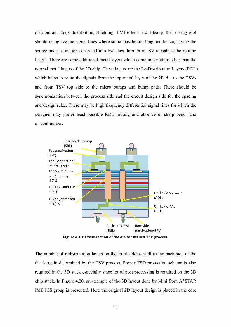
61
distribution, clock distribution, shielding, EMI effects etc. Ideally, the routing tool
should recognize the signal lines where some may be too long and hence, having the
source and destination separated into two dies through a TSV to reduce the routing
length. There are some additional metal layers which come into picture other than the
normal metal layers of the 2D chip. These layers are the Re-Distribution Layers (RDL)
which helps to route the signals from the top metal layer of the 2D die to the TSVs
and from TSV top side to the micro bumps and bump pads. There should be
synchronization between the process side and the circuit design side for the spacing
and design rules. There may be high frequency differential signal lines for which the
designer may prefer least possible RDL routing and absence of sharp bends and
discontinuities.
Figure 4.19: Cross section of the die for via last TSV process.
The number of redistribution layers on the front side as well as the back side of the
die is again determined by the TSV process. Proper ESD protection scheme is also
required in the 3D stack especially since lot of post processing is required on the 3D
chip stack. In Figure 4.20, an example of the 3D layout done by Mini from A*STAR
IME ICS group is presented. Here the original 2D layout design is placed in the core

62
of the 3D layout, and the TSV and bumps modules are placed around the core design.
Figure 4.20: Layout of one die including TSVs and bumps (from A*STAR IME ICS Group).
4.3.4 Physical Verification/Extraction
One of the most important verification steps is the physical verification of the 3D chip
which involves the Design Rule check (DRC) as well as the Layout Versus Schematic
check (LVS). For DRC check, the new layer geometries, dimensions and spacing for
the additional TSV/bump structures need to be specified in the rule file of the EDA
tool. Once the rule file is ready it needs to be integrated with the 2D design rules so
that the DRC check for the complete 3D design can be performed. If the tape out is
shared between different foundries for the core and the post processed layers, then
proper metal filling process with some keep out zone from TSVs is required. For LVS

63
check, LVS rules need to be added for the TSV and associated bump structures. There
should be continuity between the 2D and 3D LVS rules so that the check can be
performed effectively on the complete 3D stack up. Functional verification can also
be performed through simulations both in 2D and 3D domain which takes the TSV
effects into consideration. Similar to 2D extraction, 3D extraction should be able to
extract parasitic for the TSVs and bump structures. For each TSV the signal frequency,
the inter TSV coupling and TSV to substrate coupling effects should be taken into
account. Other aspects like timing analysis, clock skew, and power distribution should
also be extended to the 3D domain for timing and power critical designs so that they
can take full advantage of the 3D space.
Apart from the physical verification of the TSVs and the core circuitry, alignment
checks should also be carried out between the different dies. Proper alignment marks
should be inserted both on the die level as well as on the wafer level to ensure correct
stacking of the individual dies and thus the overall functioning of the IC stacking.
4.3.5 PCB Interface
The 3D IC stack can be mounted onto the PCB in different ways. If different process
technology nodes are involved in the design, then a silicon interposer can be used to
interface the IC stacks onto the PCB. A BGA type interface can also be used where a
substrate comes in between the micro bumps of the IC stack and the large BGA balls
that get connected to the bottom die of the IC stack instead of the substrate. There is
another option of going without the BGA substrate where the BGA balls get directly
attached to the bottom die. In Figure 4.21, the bottom die layout of the 3D IC
Transceiver is provided where the BGA pads are directly inserted as part of the die
layout.
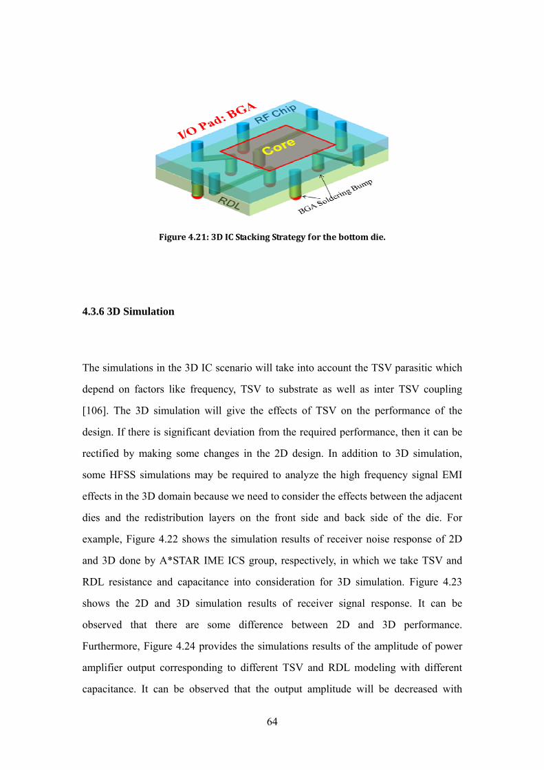
64
Figure 4.21: 3D IC Stacking Strategy for the bottom die.
4.3.6 3D Simulation
The simulations in the 3D IC scenario will take into account the TSV parasitic which
depend on factors like frequency, TSV to substrate as well as inter TSV coupling
[106]. The 3D simulation will give the effects of TSV on the performance of the
design. If there is significant deviation from the required performance, then it can be
rectified by making some changes in the 2D design. In addition to 3D simulation,
some HFSS simulations may be required to analyze the high frequency signal EMI
effects in the 3D domain because we need to consider the effects between the adjacent
dies and the redistribution layers on the front side and back side of the die. For
example, Figure 4.22 shows the simulation results of receiver noise response of 2D
and 3D done by A*STAR IME ICS group, respectively, in which we take TSV and
RDL resistance and capacitance into consideration for 3D simulation. Figure 4.23
shows the 2D and 3D simulation results of receiver signal response. It can be
observed that there are some difference between 2D and 3D performance.
Furthermore, Figure 4.24 provides the simulations results of the amplitude of power
amplifier output corresponding to different TSV and RDL modeling with different
capacitance. It can be observed that the output amplitude will be decreased with
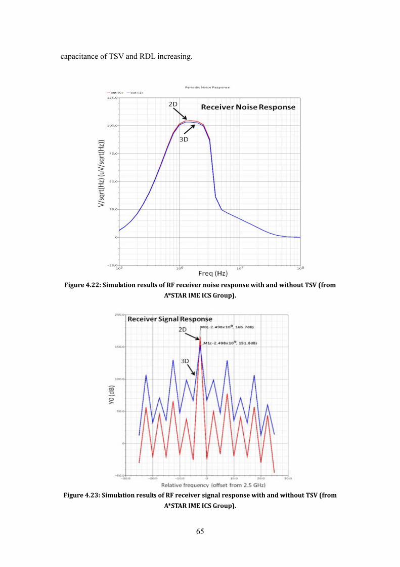
65
capacitance of TSV and RDL increasing.
Figure 4.22: Simulation results of RF receiver noise response with and without TSV (from
A*STAR IME ICS Group).
Figure 4.23: Simulation results of RF receiver signal response with and without TSV (from
A*STAR IME ICS Group).

66
Figure 4.24: RF transmitter performance with TSV and RDL layer capacitance (from A*STAR
IME ICS Group).
During design flow development, accurate modeling and characterization of the TSV,
RDL, bump and UBM are developed to extract the parasitic which is used for the
post-layout simulation to verify the performance [107]. The key performance
comparisons of wireless RF transmitter with and without TSV macro which is done
by A*STAR IME ICS group is shown in Figure 4.25. It can be observed that there is
no much performance loss due to TSV macro.
Figure 4.25: Post-layout simulation results of RF transmitter VCO and PA outputs: (a) 2D implementation; (b) 3D implementation with TSV macro (from A*STAR IME ICS Group).
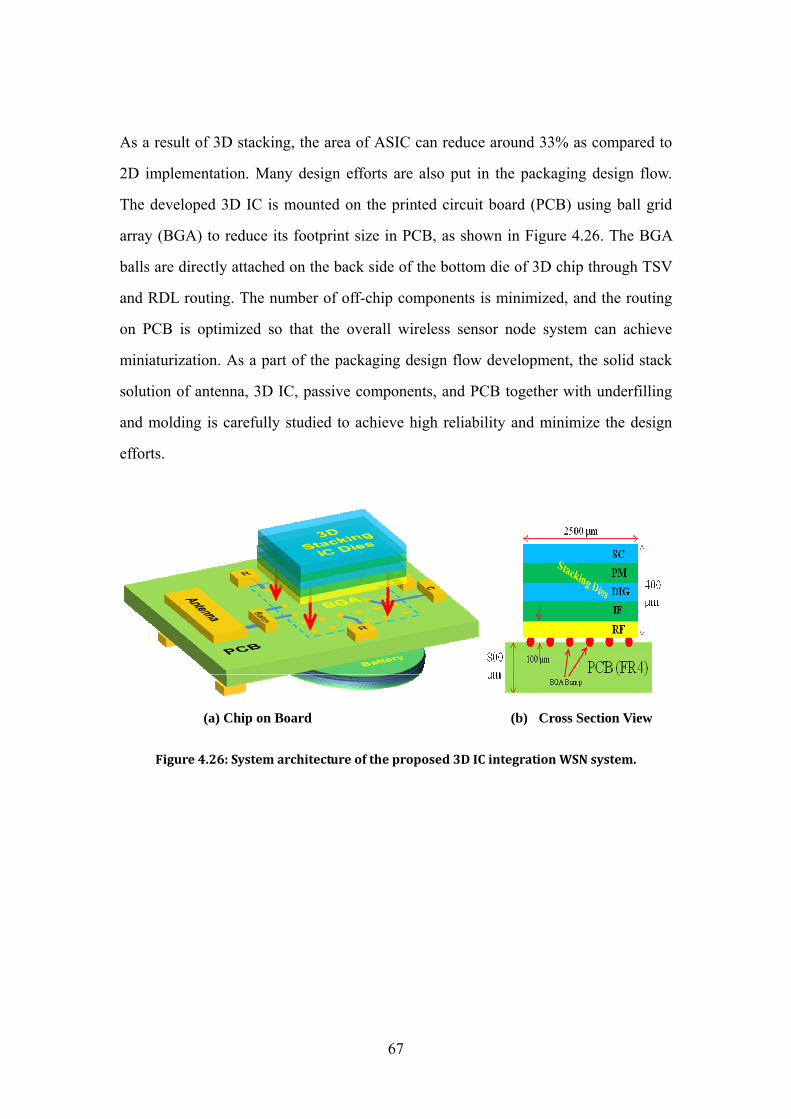
67
As a result of 3D stacking, the area of ASIC can reduce around 33% as compared to
2D implementation. Many design efforts are also put in the packaging design flow.
The developed 3D IC is mounted on the printed circuit board (PCB) using ball grid
array (BGA) to reduce its footprint size in PCB, as shown in Figure 4.26. The BGA
balls are directly attached on the back side of the bottom die of 3D chip through TSV
and RDL routing. The number of off-chip components is minimized, and the routing
on PCB is optimized so that the overall wireless sensor node system can achieve
miniaturization. As a part of the packaging design flow development, the solid stack
solution of antenna, 3D IC, passive components, and PCB together with underfilling
and molding is carefully studied to achieve high reliability and minimize the design
efforts.
(a) Chip on Board (b) Cross Section View
Figure 4.26: System architecture of the proposed 3D IC integration WSN system.

68
Chapter 5 FPGA Implementation and
Functional Tests
5.1 FPGA Implementation
Once the digital core is described in Verilog code and successfully tested in SimVision
to verify its operation prior to system integration, the digital system can be
implemented using the Field-Programmable Gate Array (FPGA). Figure 5.1 shows the
two FPGA boards engaged in this project.
Figure 5.1: FPGA board used in this design: (a) Xilinx Virtex-5; (b) Xilinx Spartan-3E.
For digital core implementation, Xilinx Virtex-5 FPGA ML505 Evaluation Platform
and Xilinx Spartan-3E XC3S1600E FPGA MicroBlaze Development Kit Board are
used for receiver and transmitter separately. The connector which has access to all the
digital I/O pins of the digital core allows other expansion boards to be connected to
add other functionality.
The digital core consists of the microcontroller, ADC interface, memory and packet
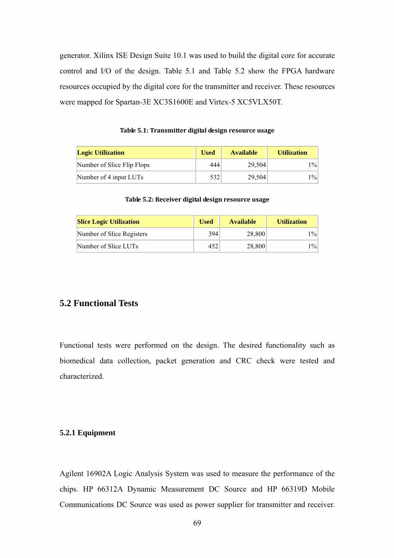
69
generator. Xilinx ISE Design Suite 10.1 was used to build the digital core for accurate
control and I/O of the design. Table 5.1 and Table 5.2 show the FPGA hardware
resources occupied by the digital core for the transmitter and receiver. These resources
were mapped for Spartan-3E XC3S1600E and Virtex-5 XC5VLX50T.
Table 5.1: Transmitter digital design resource usage
Logic Utilization Used Available Utilization
Number of Slice Flip Flops 444 29,504 1%
Number of 4 input LUTs 532 29,504 1%
Table 5.2: Receiver digital design resource usage
Slice Logic Utilization Used Available Utilization
Number of Slice Registers 394 28,800 1%
Number of Slice LUTs 452 28,800 1%
5.2 Functional Tests
Functional tests were performed on the design. The desired functionality such as
biomedical data collection, packet generation and CRC check were tested and
characterized.
5.2.1 Equipment
Agilent 16902A Logic Analysis System was used to measure the performance of the
chips. HP 66312A Dynamic Measurement DC Source and HP 66319D Mobile
Communications DC Source was used as power supplier for transmitter and receiver.

70
A picture of the equipments used is shown in Figure 5.2(a) and (b).
Figure 5.2: Test equipment: (a) Agilent logic analysis system; (b) HP DC source.
Actually, since the focus of this project is 3D IC, so in order to minimize the design
complexity, this design was based on a 2D transceiver. The 2D transceiver was
employed during the functional tests of the digital core. Since the output voltage of
FPGA is 3.3 V while VDD is 1.8 V for transceiver PCB board, a voltage divider PCB
board was used. Figure 5.3(a), Figure 5.3(b) and Figure 5.3(c) are the transceiver
boards for receiver, the voltage divider board and the transceiver boards for
transmitter.
5.2.2 Test Setup
To verify the functionality of the design, the digital core design which is described
using Verilog code was downloaded into the FPGA board which is connected to the
transceiver. Following that, test packets consisting of the preamble frame length, ID
and data payload are sent from transmitter to receiver. The architecture of the design
and the test setup used to test it are shown in Figure 5.4.
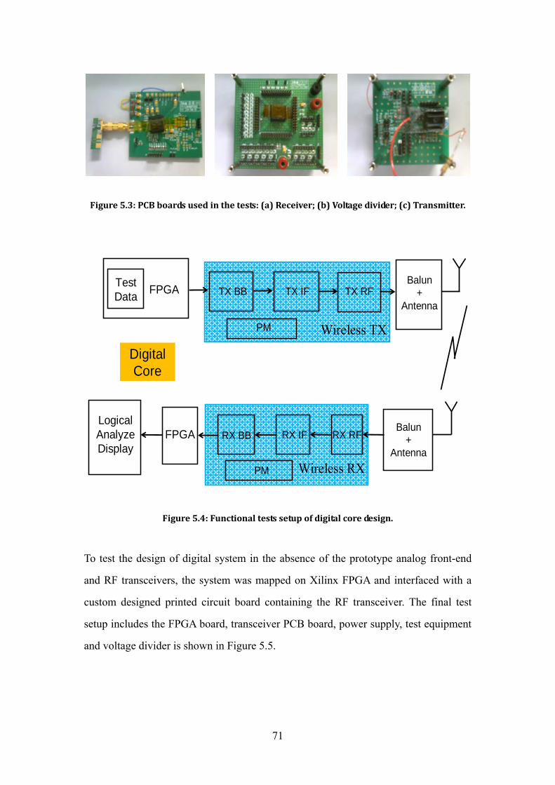
71
Figure 5.3: PCB boards used in the tests: (a) Receiver; (b) Voltage divider; (c) Transmitter.
TX BB TX IF TX RF
RX BBLogical Analyze Display
FPGA RX IF RX RF
PM
Balun+
Antenna
Digital Core
FPGATest Data
PM
Balun+
Antenna
Wireless TX
Wireless RX
Figure 5.4: Functional tests setup of digital core design.
To test the design of digital system in the absence of the prototype analog front-end
and RF transceivers, the system was mapped on Xilinx FPGA and interfaced with a
custom designed printed circuit board containing the RF transceiver. The final test
setup includes the FPGA board, transceiver PCB board, power supply, test equipment
and voltage divider is shown in Figure 5.5.
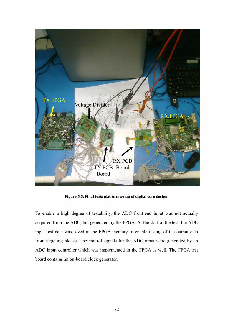
72
Figure 5.5: Final tests platform setup of digital core design.
To enable a high degree of testability, the ADC front-end input was not actually
acquired from the ADC, but generated by the FPGA. At the start of the test, the ADC
input test data was saved in the FPGA memory to enable testing of the output data
from targeting blocks. The control signals for the ADC input were generated by an
ADC input controller which was implemented in the FPGA as well. The FPGA test
board contains an on-board clock generator.
TX FPGA Voltage Divider
TX PCB Board
RX PCB Board
RX FPGA

73
5.2.3 Results
Upon the start-up of the test, the digital core of the receiver initializes the receiver by
sending a series of commands signal through the SPI bus. When the receiver is ready
to receive signals, the down conversion and synchronization process are both initiated.
The receiver begins to process the signal received from the transmitter and look for a
peak above the threshold which indicates a packet starts. When a peak above the
threshold is found, it means the synchronization point is found, and the packet will
start to be demodulated. The demodulated bits are then stored in the FIFO on chip.
When the full packet has been demodulated, an interrupt signal is sent to digital core
by the receiver which indicating that a packet has been received successfully and the
digital core may read the packet from the receiver.
After successful initialization of the receiver, the transmitter will be initialized by the
digital core through sending a series of commands signal. The control signals for the
transceiver were generated by the microcontroller in the FPGA. If the digital core
receives an EN_TX interrupt, indicating that the user would like to start to send data,
TX_ON command is sent to the transmitter by the digital core to send the data stream
the digital core writes in its FIFO. The transmitter then modulates the data from the
digital core and sends the modulated waveform to the DAC for transmission. The
transmitter then returns to waiting for the next TX_ON command.
As described in Section 5.2.1, the logic analyzer is used to display the decoded results
of the test packet. Four groups of signals were used for verification. They are: 1)
MAC_RX_BUSY, which indicates whether RX platform is in data receiving status, 2)
MAC_IRQ, MAC_SI, MAC_SCLK, MAC_CSN, MAC_SO, communication signals
between RX PCB and RX Digital Core, 3) MAC_SDOUT_VALID, that new correct
frame valid signal, and 4) MAC_DOUT_VALID, MAC_DOUT, the final continuous
8-bits parallel output. Figure 5.6 is an example of the result window of a test showing
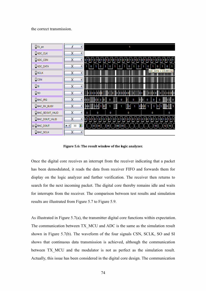
74
the correct transmission.
Figure 5.6: The result window of the logic analyzer.
Once the digital core receives an interrupt from the receiver indicating that a packet
has been demodulated, it reads the data from receiver FIFO and forwards them for
display on the logic analyzer and further verification. The receiver then returns to
search for the next incoming packet. The digital core thereby remains idle and waits
for interrupts from the receiver. The comparison between test results and simulation
results are illustrated from Figure 5.7 to Figure 5.9.
As illustrated in Figure 5.7(a), the transmitter digital core functions within expectation.
The communication between TX_MCU and ADC is the same as the simulation result
shown in Figure 5.7(b). The waveform of the four signals CSN, SCLK, SO and SI
shows that continuous data transmission is achieved, although the communication
between TX_MCU and the modulator is not as perfect as the simulation result.
Actually, this issue has been considered in the digital core design. The communication
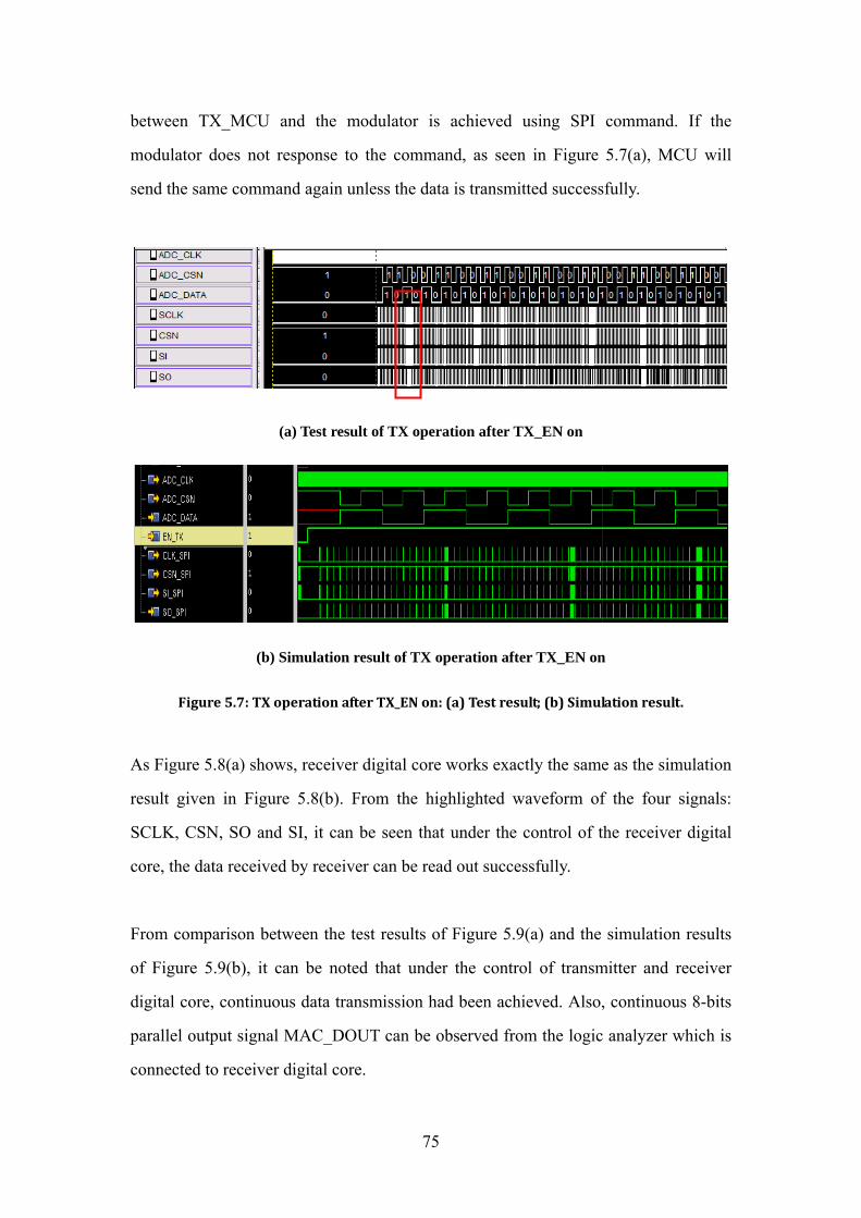
75
between TX_MCU and the modulator is achieved using SPI command. If the
modulator does not response to the command, as seen in Figure 5.7(a), MCU will
send the same command again unless the data is transmitted successfully.
(a) Test result of TX operation after TX_EN on
(b) Simulation result of TX operation after TX_EN on
Figure 5.7: TX operation after TX_EN on: (a) Test result; (b) Simulation result.
As Figure 5.8(a) shows, receiver digital core works exactly the same as the simulation
result given in Figure 5.8(b). From the highlighted waveform of the four signals:
SCLK, CSN, SO and SI, it can be seen that under the control of the receiver digital
core, the data received by receiver can be read out successfully.
From comparison between the test results of Figure 5.9(a) and the simulation results
of Figure 5.9(b), it can be noted that under the control of transmitter and receiver
digital core, continuous data transmission had been achieved. Also, continuous 8-bits
parallel output signal MAC_DOUT can be observed from the logic analyzer which is
connected to receiver digital core.
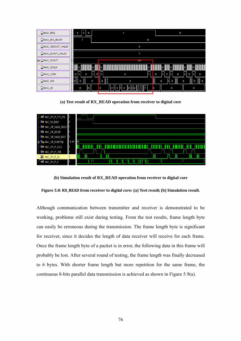
76
(a) Test result of RX_READ operation from receiver to digital core
(b) Simulation result of RX_READ operation from receiver to digital core
Figure 5.8: RX_READ from receiver to digital core: (a) Test result; (b) Simulation result.
Although communication between transmitter and receiver is demonstrated to be
working, problems still exist during testing. From the test results, frame length byte
can easily be erroneous during the transmission. The frame length byte is significant
for receiver, since it decides the length of data receiver will receive for each frame.
Once the frame length byte of a packet is in error, the following data in this frame will
probably be lost. After several round of testing, the frame length was finally decreased
to 6 bytes. With shorter frame length but more repetition for the same frame, the
continuous 8-bits parallel data transmission is achieved as shown in Figure 5.9(a).
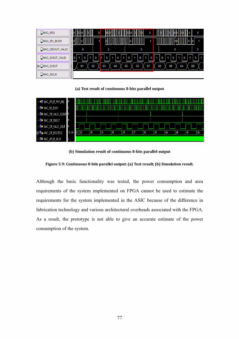
77
(a) Test result of continuous 8-bits parallel output
(b) Simulation result of continuous 8-bits parallel output
Figure 5.9: Continuous 8-bits parallel output: (a) Test result; (b) Simulation result.
Although the basic functionality was tested, the power consumption and area
requirements of the system implemented on FPGA cannot be used to estimate the
requirements for the system implemented in the ASIC because of the difference in
fabrication technology and various architectural overheads associated with the FPGA.
As a result, the prototype is not able to give an accurate estimate of the power
consumption of the system.

78
Chapter 6 Conclusions and Future Work
6.1 Conclusions
In this research, innovative 3D IC technology was employed as a basic tool to develop
miniaturized wireless sensors. In addition to the conventional horizontal dimension,
active devices are stacked in the vertical dimension in 3D IC technology. The
additional degree of connectivity in the vertical dimension enables circuit designers to
replace long horizontal wires with short vertical interconnects, so that delay, power
consumption, and area can be reduced.
A novel design flow, which is the key innovation realized in this research work, had
been devised for the 3D mixed-signal circuit design. The approach had been
successfully verified to be feasibly for 3D implementations, base on the existing
technology and tools. The proposed design methodologies described in this thesis are
intended to strengthen the 3D design capabilities, making this fascinating technology
a promising solution for future integrated systems. The method was proven via the
proposed 3D wireless sensor node.
Second, the space challenges faced by the 3D IC design during front-end design are
evaluated in this research. The 3D architecture for a wireless sensor node had been
discussed thoroughly and the impact of the 3D-integration technology on the
conventional digital circuit design was demonstrated. Through silicon via (TSV)
based 3D integration technology was employed for the vertical interconnection for the
proposed 3D wireless sensor node. Since 3D stacking with TSV may increase the total
die area, the optimizations of TSV and IO number of the system had been considered

79
in the proposed design flow. Through block repartition in digital core design, the
number of IO of each portion in the system is reduced. Significant enhancements on
the existing 2D design and verification flow were also developed to solve many
critical issues of the heterogeneous 3D IC integration, including block-level
partitioning, TSV macro design, TSV-related modeling and characterization. The area
of the proposed 3D IC is reduced by around 33% as compared to the 2D
implementation, and the complete wireless sensor node system is miniaturized.
Finally, a novel and innovative 3D wireless sensor node was designed. The design
problems of the miniaturized wireless sensor node were investigated and a digital core
design in wireless sensor node was proposed. The proposed digital core design in 3D
wireless sensor node was implemented in FPGA. Test was conducted to validate the
overall systems usability and modularity. From the comparison between the test
results and the simulation results, it can be observed that both transmitter and receiver
were able to function as expected. Under the control of microcontroller in the system,
continuous data transmit is implemented. Also, continuous 8-bits parallel output can
be obtained in the receiver. These results validate the approaches chosen, and showed
that the system is useful in patient monitoring application.
6.2 Further Work
6.2.1 Early Planning and Estimation Tools for 3D IC Design
3D IC implementations have so far been limited to niche applications such as CMOS
Imagers and DRAMs products. However, recent advances related to TSV
(Through-Silicon-Via), RDL (Redistribution Layer) and micro-bumping opened the

80
door to new opportunities and made 3D IC technology an option for a wider class of
applications. These new opportunities come also with a new set of challenges in terms
of design, fabrication and test.
On the design side, although design methodologies are discussed and a 3D circuit
design flow is proposed in this thesis, significant effort is still required to strengthen
3D design capabilities, making this fascinating technology a promising solution for
future integrated systems. The need for tools and methodologies for early planning
and estimations of area, performance, power and cost is vital and has been clearly
identified by the industry as a key component for 3D IC design to become main
stream. So one of the future works is to close the loop with the estimation tools and
methodologies, ensure the right calibrations and the silicon-proof on real life 3D ICs.
The necessary models, tools and methodologies to enable designers to do the
architectural exploration and hardware partitioning in order to determine and refine
the optimal 3D implementation of the system will be defined and implemented.
Improvement of models, equations and heuristics will have to go through several
iterations. Finally, the estimator will be programmed with a user friendly interface and
the capability of comparing several implementations to allow the designer to converge
toward the optimal 3D implementation based on merits such as area, power,
performance and cost.
6.2.2 Low Power Digital Core Design
A possible future work on the digital core can be to focus on the energy improvements
by using standby mode operation [77]. The use of the standby mode operation has not
been conducted in previous wireless sensor network hardware mainly because of the
focus in minimizing the design complexity.

81
Many sensor measurements do not need to be taken continuously since environmental
conditions can be periodically sampled. Even when the sensor nodes need to forward
data from other sensors in the same wireless network, it is likely that a sensor node
can be idle for long periods of time. Turning off unnecessary circuitries during these
idle periods is necessary to meet the total energy budget of miniature sensor systems.
The sensor front end and wireless communication can be power gated, eliminating
static currents used in amplifiers and reducing leakage in sensors and ADC circuitry.
The microprocessor can also be power gated. If the duty cycle of the sensor node is
low, the total system power will be dominated by the standby mode power. Sensors
with standby power as low as 30 pW has already been reported [108].
Other digital power saving techniques can also be pursued. VDD scaling is perhaps
the most effective way of reducing the processor power, with several designs
achieving 2 pJ per instruction [47, 48, 108]. Voltage scaling also has a strong effect on
energy consumption since the dynamic switching energy of the microprocessor scales
with VDD. Both of these power saving techniques however, do require some extra
steps in the digital circuit design flow, such as clock-gating and power gating logic
insertion [108], linear regulators design and buck regulator design [77].
82
References
[1] J. Burns, L. McIlrath, C. Keast, C. Lewis, A. Loomis, K. Warner, and P. Wyatt,
"Three-dimensional integrated circuits for low-power, high-bandwidth systems on a chip," 2001, pp. 268-269, 453.
[2] K. Banerjee, S. J. Souri, P. Kapur, and K. C. Saraswat, "3-D ICs: A novel chip design for improving deep-submicrometer interconnect performance and systems-on-chip integration," Proceedings of the IEEE, vol. 89, pp. 602-633, 2001.
[3] A. Zeitouny, M. Eizenberg, S. Pearton, and F. Ren, "Contact resistivity and transport mechanisms in W contacts to p-and n-GaN," Journal of Applied Physics, vol. 88, p. 2048, 2000.
[4] B. Luo, F. Ren, R. Fitch, J. Gillespie, T. Jenkins, J. Sewell, D. Via, A. Crespo, A. Baca, and R. Briggs, "Improved morphology for ohmic contacts to AlGaN/GaN high electron mobility transistors using WSi-or W-based metallization," Applied Physics Letters, vol. 82, p. 3910, 2003.
[5] P. Reed, G. Yeung, and B. Black, "Design aspects of a microprocessor data cache using 3D die interconnect technology," 2005, pp. 15-18.
[6] K. Puttaswamy and G. H. Loh, "Implementing caches in a 3D technology for high performance processors," 2005, pp. 525-532.
[7] Y. F. Tsai, Y. Xie, N. Vijaykrishnan, and M. J. Irwin, "Three-dimensional cache design exploration using 3DCacti," pp. 519-524.
[8] K. Puttaswamy and G. H. Loh, "Thermal analysis of a 3D die-stacked high-performance microprocessor," 2006, pp. 19-24.
[9] A. Zeng, J. Lu, K. Rose, and R. J. Gutmann, "First-order performance prediction of cache memory with wafer-level 3D integration," Design & Test of Computers, IEEE, vol. 22, pp. 548-555, 2005.
[10] K. Puttaswamy and G. H. Loh, "Dynamic instruction schedulers in a 3-dimensional integration technology," 2006, pp. 153-158.
[11] Y. Xie, G. H. Loh, B. Black, and K. Bernstein, "Design space exploration for 3D architectures," ACM Journal on Emerging Technologies in Computing Systems (JETC), vol. 2, pp. 65-103, 2006.
[12] K. Puttaswamy and G. H. Loh, "The impact of 3-dimensional integration on the design of arithmetic units," 2006, p. 4 pp.
[13] J. W. Joyner, R. Venkatesan, P. Zarkesh-Ha, J. A. Davis, and J. D. Meindl, "Impact of three-dimensional architectures on interconnects in gigascale integration," Very Large Scale Integration (VLSI) Systems, IEEE Transactions on, vol. 9, pp. 922-928, 2001.
[14] R. S. Patti, "Three-dimensional integrated circuits and the future of system-on-chip designs," Proceedings of the IEEE, vol. 94, pp. 1214-1224, 2006.
[15] R. Zhang, K. Roy, C. K. Koh, and D. B. Janes, "Power trends and performance characterization of 3-dimensional integration for future technology generations," 2001, p. 217.
[16] J. A. Davis, R. Venkatesan, A. Kaloyeros, M. Beylansky, S. J. Souri, K. Banerjee, K. C.
83
Saraswat, A. Rahman, R. Reif, and J. D. Meindl, "Interconnect limits on gigascale integration (GSI) in the 21st century," Proceedings of the IEEE, vol. 89, pp. 305-324, 2001.
[17] P. Emma and E. Kursun, "Is 3D chip technology the next growth engine for performance improvement?," IBM Journal of Research and Development, vol. 52, pp. 541-552, 2008.
[18] R. Lauwereins. (2008). Will 3D stacking of ICs enable to continue Moore's momentum in the 21st century? Available: http://www.mpsoc-forum.org/2008/slides/6-3%20Lauwereins.pdf
[19] N. Magen, A. Kolodny, U. Weiser, and N. Shamir, "Interconnect-power dissipation in a microprocessor," 2004, pp. 7-13.
[20] J. Ouyang, G. Sun, Y. Chen, L. Duan, T. Zhang, Y. Xie, and M. Irwin, "Arithmetic unit design using 180nm TSV-based 3D stacking technology," 2009, pp. 1-4.
[21] B. Black, M. Annavaram, N. Brekelbaum, J. DeVale, L. Jiang, G. H. Loh, D. McCaule, P. Morrow, D. W. Nelson, and D. Pantuso, "Die stacking (3D) microarchitecture," 2006, pp. 469-479.
[22] T. Kgil, S. D'Souza, A. Saidi, N. Binkert, R. Dreslinski, T. Mudge, S. Reinhardt, and K. Flautner, "PicoServer: using 3D stacking technology to enable a compact energy efficient chip multiprocessor," ACM SIGPLAN Notices, vol. 41, pp. 117-128, 2006.
[23] J. W. Joyner, P. Zarkesh-Ha, and J. D. Meindl, "A stochastic global net-length distribution for a three-dimensional system-on-a-chip (3D-SoC)," 2001, pp. 147-151.
[24] B. Vaidyanathan, W. L. Hung, F. Wang, Y. Xie, V. Narayanan, and M. J. Irwin, "Architecting microprocessor components in 3D design space," 2007.
[25] K. Puttaswamyt and G. H. Loh, "Scalability of 3D-integrated arithmetic units in high-performance microprocessors," 2007, pp. 622-625.
[26] J. Mayega, O. Erdogan, P. M. Belemjian, K. Zhou, J. F. McDonald, and R. P. Kraft, "3D direct vertical interconnect microprocessors test vehicle," 2003, pp. 141-146.
[27] B. Black, D. W. Nelson, C. Webb, and N. Samra, "3D processing technology and its impact on iA32 microprocessors," 2004.
[28] K. Puttaswamy and G. H. Loh, "Implementing register files for high-performance microprocessors in a die-stacked (3D) technology," 2006.
[29] M. Mondal, A. J. Ricketts, S. Kirolos, T. Ragheb, G. Link, N. Vijaykrishnan, and Y. Massoud, "Thermally robust clocking schemes for 3D integrated circuits," 2007, pp. 1206-1211.
[30] G. L. Loi, B. Agrawal, N. Srivastava, S. C. Lin, T. Sherwood, and K. Banerjee, "A thermally-aware performance analysis of vertically integrated (3-D) processor-memory hierarchy," 2006, pp. 991-996.
[31] C. C. Liu, I. Ganusov, M. Burtscher, and S. Tiwari, "Bridging the processor-memory performance gap with 3D IC technology," Design & Test of Computers, IEEE, vol. 22, pp. 556-564, 2005.
[32] K. Puttaswamy and G. H. Loh, "Thermal herding: Microarchitecture techniques for controlling hotspots in high-performance 3d-integrated processors," 2007, pp. 193-204.
[33] S. Mysore, B. Agrawal, N. Srivastava, S. C. Lin, K. Banerjee, and T. Sherwood, "Introspective 3D chips," ACM SIGOPS Operating Systems Review, vol. 40, pp. 264-273, 2006.
[34] Y. S. Deng and W. Maly, "2.5 D system integration: a design driven system implementation schema," 2004.
[35] A. Rahman and R. Reif, "System-level performance evaluation of three-dimensional integrated circuits," Very Large Scale Integration (VLSI) Systems, IEEE Transactions on, vol.
84
8, pp. 671-678, 2000. [36] M. Lin, A. El Gamal, Y. C. Lu, and S. Wong, "Performance benefits of monolithically stacked
3-D FPGA," Computer-Aided Design of Integrated Circuits and Systems, IEEE Transactions on, vol. 26, pp. 216-229, 2007.
[37] C. Ababei, H. Mogal, and K. Bazargan, "Three-dimensional place and route for FPGAs," 2005, pp. 773-778.
[38] M. Lin and A. El Gamal, "A routing fabric for monolithically stacked 3D-FPGA," 2007, pp. 3-12.
[39] L. Cheng, L. Deng, and M. D. F. Wong, "Floorplanning for 3-D VLSI design," 2005, pp. 405-411.
[40] J. Cong and Y. Zhang, "Thermal-driven multilevel routing for 3-D ICs," 2005, pp. 121-126. [41] S. Das, A. Fan, K. N. Chen, C. S. Tan, N. Checka, and R. Reif, "Technology, performance, and
computer-aided design of three-dimensional integrated circuits," 2004, pp. 108-115. [42] B. Goplen and S. Sapatnekar, "Efficient thermal placement of standard cells in 3D ICs using a
force directed approach," 2003, p. 86. [43] B. Black, D. W. Nelson, C. Webb, and N. Samra, "3D processing technology and its impact on
iA32 microprocessors," 2004, pp. 316-318. [44] J. Cong, J. Wei, and Y. Zhang, "A thermal-driven floorplanning algorithm for 3D ICs," 2004,
pp. 306-313. [45] S. Das, A. Chandrakasan, and R. Reif, "Design tools for 3-D integrated circuits," 2003, pp.
53-56. [46] W. L. Hung, G. Link, Y. Xie, N. Vijaykrishnan, and M. Irwin, "Interconnect and thermal-aware
floorplanning for 3D microprocessors," 2006. [47] S. C. Jocke, J. F. Bolus, S. N. Wooters, A. Jurik, A. Weaver, T. Blalock, and B. Calhoun, "A
2.6-¦ÌW sub-threshold mixed-signal ECG SoC," 2009, pp. 60-61. [48] J. Kwong, Y. K. Ramadass, N. Verma, and A. P. Chandrakasan, "A 65 nm Sub-Vt
Microcontroller With Integrated SRAM and Switched Capacitor DC-DC Converter," Solid-State Circuits, IEEE Journal of, vol. 44, pp. 115-126, 2009.
[49] Die Stacking. Available: http://www.siliconfareast.com/diestacking.htm [50] S. H. Christiansen, R. Singh, and U. Gosele, "Wafer direct bonding: From advanced substrate
engineering to future applications in micro/nanoelectronics," Proceedings of the IEEE, vol. 94, pp. 2060-2106, 2006.
[51] FaStack® Creates 3D Integrated Circuits (3D-ICs). Available: http://www.tezzaron.com/technology/FaStack.htm
[52] R. Goering. (2010). A Reality Check On 3D ICs. Available: http://www.cadence.com/Community/blogs/ii/archive/2010/04/19/eda-workshop-a-reality-check-on-3d-ics.aspx
[53] C. Ababei, Y. Feng, B. Goplen, H. Mogal, T. Zhang, K. Bazargan, and S. Sapatnekar, "Placement and routing in 3D integrated circuits," Design & Test of Computers, IEEE, vol. 22, pp. 520-531, 2005.
[54] J. W. Joyner and J. D. Meindl, "Opportunities for reduced power dissipation using three-dimensional integration," 2002, pp. 148-150.
[55] W. R. Davis, J. Wilson, S. Mick, J. Xu, H. Hua, C. Mineo, A. M. Sule, M. Steer, and P. D. Franzon, "Demystifying 3D ICs: the pros and cons of going vertical," Design & Test of
85
Computers, IEEE, vol. 22, pp. 498-510, 2005. [56] R. Reif, A. Fan, K. N. Chen, and S. Das, "Fabrication technologies for three-dimensional
integrated circuits," 2002, p. 33. [57] K. Lee, T. Nakamura, T. Ono, Y. Yamada, T. Mizukusa, H. Hashimoto, K. Park, H. Kurino,
and M. Koyanagi, "Three-dimensional shared memory fabricated using wafer stacking technology," 2000, pp. 165-168.
[58] J. Kim, C. Nicopoulos, D. Park, R. Das, Y. Xie, V. Narayanan, M. S. Yousif, and C. R. Das, "A novel dimensionally-decomposed router for on-chip communication in 3D architectures," ACM SIGARCH Computer Architecture News, vol. 35, pp. 138-149, 2007.
[59] I. F. Akyildiz, W. Su, Y. Sankarasubramaniam, and E. Cayirci, "A survey on sensor networks," Communications Magazine, IEEE, vol. 40, pp. 102-114, 2002.
[60] G. J. Pottie, "Wireless integrated network sensors (wins): the web gets physical," Frontiers of engineering, p. 78, 2002.
[61] S. Park, A. Savvides, and M. B. Srivastava, "SensorSim: a simulation framework for sensor networks," 2000, pp. 104-111.
[62] J. M. Kahn, R. H. Katz, and K. S. J. Pister, "Mobile networking for smart dust," 1999. [63] J. M. Rabaey, M. J. Ammer, J. L. da Silva Jr, D. Patel, and S. Roundy, "PicoRadio supports ad
hoc ultra-low power wireless networking," Computer, vol. 33, pp. 42-48, 2000. [64] O. Omeni, A. Wong, A. J. Burdett, and C. Toumazou, "Energy efficient medium access
protocol for wireless medical body area sensor networks," Biomedical Circuits and Systems, IEEE Transactions on, vol. 2, pp. 251-259, 2008.
[65] P. Juang, H. Oki, Y. Wang, M. Martonosi, L. S. Peh, and D. Rubenstein, "Energy-efficient computing for wildlife tracking: design tradeoffs and early experiences with ZebraNet," 2002, pp. 96-107.
[66] A. Cerpa, J. Elson, D. Estrin, L. Girod, M. Hamilton, and J. Zhao, "Habitat monitoring: Application driver for wireless communications technology," ACM SIGCOMM Computer Communication Review, vol. 31, pp. 20-41, 2001.
[67] D. J. Anthony, W. P. Bennett, M. C. Vuran, M. B. Dwyer, S. Elbaum, and F. Chavez-Ramirez, "Simulating and testing mobile wireless sensor networks," 2010, pp. 49-58.
[68] E. S. Biagioni and K. Bridges, "The application of remote sensor technology to assist the recovery of rare and endangered species," International Journal of High Performance Computing Applications, vol. 16, p. 315, 2002.
[69] A. Mainwaring, D. Culler, J. Polastre, R. Szewczyk, and J. Anderson, "Wireless sensor networks for habitat monitoring," 2002, pp. 88-97.
[70] G. Werner-Allen, J. Johnson, M. Ruiz, J. Lees, and M. Welsh, "Monitoring volcanic eruptions with a wireless sensor network," 2005, pp. 108-120.
[71] W. Tsujita, S. Kaneko, T. Ueda, H. Ishida, and T. Moriizumi, "Sensor-based air-pollution measurement system for environmental monitoring network," 2003, pp. 544-547 vol. 1.
[72] P. Rentala, R. Musunuri, S. Gandham, and U. Saxena, "Survey on sensor networks," 2001. [73] C. R. Farrar and K. Worden, "An introduction to structural health monitoring," Philosophical
Transactions of the Royal Society A: Mathematical, Physical and Engineering Sciences, vol. 365, p. 303, 2007.
[74] M. Maroti, G. Simon, A. Ledeczi, and J. Sztipanovits, "Shooter localization in urban terrain," Computer, vol. 37, pp. 60-61, 2004.
86
[75] D. Malan, T. Fulford-Jones, M. Welsh, and S. Moulton, "Codeblue: An ad hoc sensor network infrastructure for emergency medical care," Organization co-chairs, 2004.
[76] T. G ttsche, M. Gr fe, and P. Osypka, "HYPER-IMS-An Implantable Medical Device for Wireless Pressure Monitoring," Smart Systems, p. 19.
[77] G. Chen, S. Hanson, D. Blaauw, and D. Sylvester, "Circuit design advances for wireless sensing applications," Proceedings of the IEEE, vol. 98, pp. 1808-1827, 2010.
[78] I. F. Akyildiz, T. Melodia, and K. R. Chowdury, "Wireless multimedia sensor networks: A survey," Wireless Communications, IEEE, vol. 14, pp. 32-39, 2007.
[79] J. L. Hill, "System architecture for wireless sensor networks," Citeseer, 2003. [80] L. Nachman, J. Huang, J. Shahabdeen, R. Adler, and R. Kling, "Imote2: Serious computation
at the edge," 2008, pp. 1118-1123. [81] A. Wheeler, "Commercial applications of wireless sensor networks using ZigBee,"
Communications Magazine, IEEE, vol. 45, pp. 70-77, 2007. [82] A. Phani Kumar and V. Reddy, "Distributed collaboration for event detection in wireless
sensor networks," 2005, pp. 1-8. [83] K. Wu, Y. Gao, F. Li, and Y. Xiao, "Lightweight deployment-aware scheduling for wireless
sensor networks," Mobile networks and applications, vol. 10, pp. 837-852, 2005. [84] Z. B. Alliance, "ZigBee specification 2006," ZigBee Document, 053474r17, 2008. [85] E. Monton, J. Hernandez, J. Blasco, T. Herve, J. Micallef, I. Grech, A. Brincat, and V. Traver,
"Body area network for wireless patient monitoring," Communications, IET, vol. 2, pp. 215-222, 2008.
[86] R. Zheng, J. C. Hou, and L. Sha, "Performance analysis of power management policies in wireless networks," Wireless Communications, IEEE Transactions on, vol. 5, pp. 1351-1361, 2006.
[87] C. Schurgers, V. Tsiatsis, S. Ganeriwal, and M. Srivastava, "Optimizing sensor networks in the energy-latency-density design space," IEEE transactions on mobile computing, pp. 70-80, 2002.
[88] M. J. Miller and N. H. Vaidya, "A MAC protocol to reduce sensor network energy consumption using a wakeup radio," IEEE transactions on mobile computing, pp. 228-242, 2005.
[89] A. Sinha and A. Chandrakasan, "Dynamic power management in wireless sensor networks," Design & Test of Computers, IEEE, vol. 18, pp. 62-74, 2001.
[90] K. Akkaya and M. Younis, "A survey on routing protocols for wireless sensor networks," Ad Hoc Networks, vol. 3, pp. 325-349, 2005.
[91] B. Chen, K. Jamieson, H. Balakrishnan, and R. Morris, "Span: An energy-efficient coordination algorithm for topology maintenance in ad hoc wireless networks," Wireless Networks, vol. 8, pp. 481-494, 2002.
[92] C. Hsin and M. Liu, "Network coverage using low duty-cycled sensors: random & coordinated sleep algorithms," 2004, pp. 433-442.
[93] A. Chamam and S. Pierre, "Energy-efficient state scheduling for maximizing sensor network lifetime under coverage constraint," 2007, pp. 63-63.
[94] A. Buczak and V. Jamalabad, "Self-organization of a heterogeneous sensor network by genetic algorithms," Intelligent Engineering Systems Through Artificial Neural Networks, vol. 8, pp. 259-264, 1998.
87
[95] S. Pattem and B. Krishnamachari, "Energy-quality tradeoffs in sensor tracking: selective activation with noisy measurements," 2003.
[96] Part 15.4: wireless medium access control (MAC) and physical layer (PHY) specifications for low-rate wireless personal area networks (LR-WPANs). New York: The Institute of Electrical and Electronics Engineers, 2003.
[97] G. G. E. Gielen and R. A. Rutenbar, "Computer-aided design of analog and mixed-signal integrated circuits," Proceedings of the IEEE, vol. 88, pp. 1825-1854, 2000.
[98] H. Kaeslin, Digital integrated circuit design: from VLSI architectures to CMOS fabrication: Cambridge Univ Pr, 2008.
[99] J. Cong, "3D IC Design Tools and Applications to Microarchitecture Exploration." [100] R. Maheshwary. (2009). 3D Stacking: EDA Challenges & Opportunities. Available:
http://www.sematech.org/meetings/archives/symposia/8845/05_Rajiv%20Maheshwary%20of%20Synopsys.pdf
[101] N. Khan, V. S. Rao, S. Lim, H. S. We, V. Lee, X. Zhang, E. Liao, R. Nagarajan, T. Chai, and V. Kripesh, "Development of 3-D silicon module with TSV for system in packaging," Components and Packaging Technologies, IEEE Transactions on, vol. 33, pp. 3-9, 2010.
[102] Y. J. Lee and S. K. Lim, "Co-optimization of signal, power, and thermal distribution networks for 3D ICs," 2008, pp. 163-166.
[103] M. S. Bakir, C. King, D. Sekar, H. Thacker, B. Dang, G. Huang, A. Naeemi, and J. D. Meindl, "3D heterogeneous integrated systems: liquid cooling, power delivery, and implementation," 2008, pp. 663-670.
[104] K. Kumagai, Y. Yoneda, H. Izumino, H. Shimojo, M. Sunohara, T. Kurihara, M. Higashi, and Y. Mabuchi, "A Silicon interposer BGA package with Cu-filled TSV and multi-layer Cu-plating interconnect," 2008, pp. 571-576.
[105] D. H. Kim, K. Athikulwongse, and S. K. Lim, "A study of through-silicon-via impact on the 3D stacked IC layout," 2009, pp. 674-680.
[106] M. B. Healy and S. K. Lim, "A study of stacking limit and scaling in 3D ICs: An interconnect perspective," 2009, pp. 1213-1220.
[107] G. Katti, M. Stucchi, K. De Meyer, and W. Dehaene, "Electrical modeling and characterization of through silicon via for three-dimensional ICs," Electron Devices, IEEE Transactions on, vol. 57, pp. 256-262, 2010.
[108] S. Hanson, M. Seok, Y. S. Lin, Z. Y. Foo, D. Kim, Y. Lee, N. Liu, D. Sylvester, and D. Blaauw, "A low-voltage processor for sensing applications with picowatt standby mode," Solid-State Circuits, IEEE Journal of, vol. 44, pp. 1145-1155, 2009.

88
Publication List
1. Xin Liu, Lei Wang, Mini Jayakrishnan, Jingjing Lan, Hongyu Li, Chong Ser
Choong, Raja Muthusamy Kumarasamy, Yongxin Guo, Wang Ling Goh, Shan
Gao, and Minkyu Je, “A Miniaturized Heterogeneous Wireless Sensor Node in
3DIC”, IEEE International 3D System Integration Conference 2011 (3DIC
2011), 31 Jan to 2 Feb 2012, Osaka, Japan. Published in session 7-4.
2. Mini Jayakrishnan, Xin Liu, Hong Yu Li, Jingjing Lan, Wang Ling Goh,
“Physical Design Exploration of 3DIC Wireless Transceiver using
Through-Si-Vias”, 13th International Symposium on Integrated Circuits (ISIC
2011), December 12 to 14, Singapore, pp. 470–473.
3. Jingjing Lan, Wang Ling Goh, Zhi Hui Kong and Kiat Seng Yeo, “A Random
Number Generator for Low Power Cryptographic Application”, 7th
International SoC Design Conference (ISOCC 2010), November 22 to 23,
Songdo ConvensiA, Incheon, Korea - Best Paper Award, pp. 328–331.

89
Appendices
Appendix A: Verilog RTL code of ADC interface for transmitter
////////////////
// TOP MODULE //
////////////////
module BPRO_TX_BB_MAC_ADC_IF (
CLK1M,
CLK1K,
RSTN,
EN_TX,
CLK1M_CNT_9B,
ADC_DATA,
ADC_CLK, // 1MHz
ADC_CSN,
BP_SHIFT
);
////////////
// INPUTS //
////////////
input CLK1M;
input CLK1K;
input RSTN;
input EN_TX;
input [8:0] CLK1M_CNT_9B;
input ADC_DATA;
/////////////
// OUTPUTS //
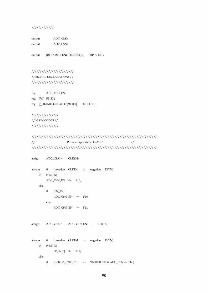
90
/////////////
output ADC_CLK;
output ADC_CSN;
output [((FRAME_LENGTH-3)*8-1):0] BP_SHIFT;
/////////////////////////
// SIGNAL DECLARATIONS //
/////////////////////////
reg ADC_CSN_EN;
reg [7:0] BP_IN;
reg [((FRAME_LENGTH-3)*8-1):0] BP_SHIFT;
////////////////
// MAIN CODES //
////////////////
//////////////////////////////////////////////////////////////////////////
// Provide input signal to ADC //
//////////////////////////////////////////////////////////////////////////
assign ADC_CLK = CLK1M;
always @ (posedge CLK1K or negedge RSTN)
if (~RSTN)
ADC_CSN_EN <= 1'b1;
else
if (EN_TX)
ADC_CSN_EN <= 1'b0;
else
ADC_CSN_EN <= 1'b1;
assign ADC_CSN = ADC_CSN_EN | CLK1K;
always @ (posedge CLK1M or negedge RSTN)
if (~RSTN)
BP_IN[7] <= 1'b0;
else
if (CLK1M_CNT_9B == 9'b000000100 & ADC_CSN == 1'b0)
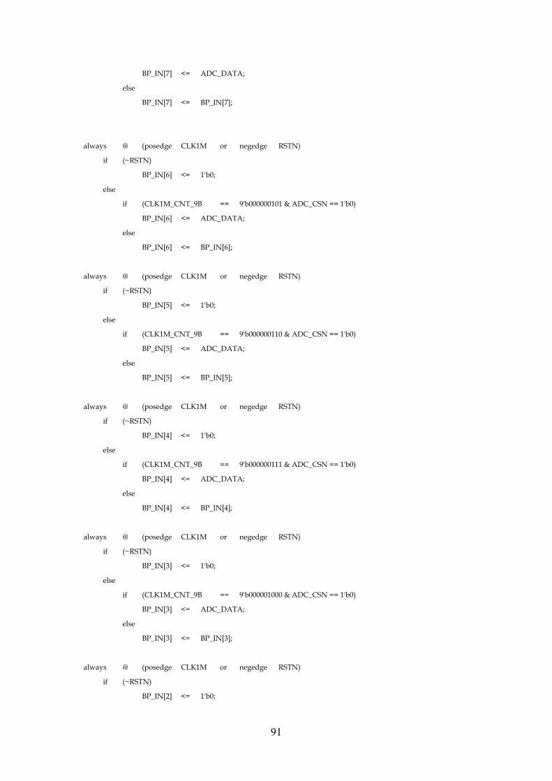
91
BP_IN[7] <= ADC_DATA;
else
BP_IN[7] <= BP_IN[7];
always @ (posedge CLK1M or negedge RSTN)
if (~RSTN)
BP_IN[6] <= 1'b0;
else
if (CLK1M_CNT_9B == 9'b000000101 & ADC_CSN == 1'b0)
BP_IN[6] <= ADC_DATA;
else
BP_IN[6] <= BP_IN[6];
always @ (posedge CLK1M or negedge RSTN)
if (~RSTN)
BP_IN[5] <= 1'b0;
else
if (CLK1M_CNT_9B == 9'b000000110 & ADC_CSN == 1'b0)
BP_IN[5] <= ADC_DATA;
else
BP_IN[5] <= BP_IN[5];
always @ (posedge CLK1M or negedge RSTN)
if (~RSTN)
BP_IN[4] <= 1'b0;
else
if (CLK1M_CNT_9B == 9'b000000111 & ADC_CSN == 1'b0)
BP_IN[4] <= ADC_DATA;
else
BP_IN[4] <= BP_IN[4];
always @ (posedge CLK1M or negedge RSTN)
if (~RSTN)
BP_IN[3] <= 1'b0;
else
if (CLK1M_CNT_9B == 9'b000001000 & ADC_CSN == 1'b0)
BP_IN[3] <= ADC_DATA;
else
BP_IN[3] <= BP_IN[3];
always @ (posedge CLK1M or negedge RSTN)
if (~RSTN)
BP_IN[2] <= 1'b0;
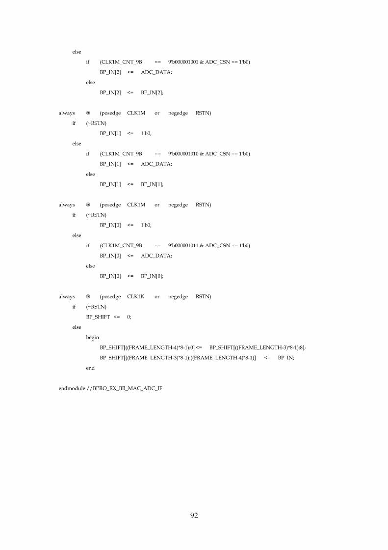
92
else
if (CLK1M_CNT_9B == 9'b000001001 & ADC_CSN == 1'b0)
BP_IN[2] <= ADC_DATA;
else
BP_IN[2] <= BP_IN[2];
always @ (posedge CLK1M or negedge RSTN)
if (~RSTN)
BP_IN[1] <= 1'b0;
else
if (CLK1M_CNT_9B == 9'b000001010 & ADC_CSN == 1'b0)
BP_IN[1] <= ADC_DATA;
else
BP_IN[1] <= BP_IN[1];
always @ (posedge CLK1M or negedge RSTN)
if (~RSTN)
BP_IN[0] <= 1'b0;
else
if (CLK1M_CNT_9B == 9'b000001011 & ADC_CSN == 1'b0)
BP_IN[0] <= ADC_DATA;
else
BP_IN[0] <= BP_IN[0];
always @ (posedge CLK1K or negedge RSTN)
if (~RSTN)
BP_SHIFT <= 0;
else
begin
BP_SHIFT[((FRAME_LENGTH-4)*8-1):0] <= BP_SHIFT[((FRAME_LENGTH-3)*8-1):8];
BP_SHIFT[((FRAME_LENGTH-3)*8-1):((FRAME_LENGTH-4)*8-1)] <= BP_IN;
end
endmodule //BPRO_RX_BB_MAC_ADC_IF

93
Appendix B: Verilog RTL code of ID generator for transmitter
////////////////
// TOP MODULE //
////////////////
module BPRO_TX_BB_MAC_ID_GEN (
//input
CLK1M,
CLK1K,
RSTN,
EN_TX,
//output
ID_BYTE,
DATA_VALID
);
////////////
// INPUTS //
////////////
input CLK1M;
input CLK1K;
input RSTN;
input EN_TX;
/////////////
// OUTPUTS //
/////////////
output [7:0] ID_BYTE;
output DATA_VALID;
/////////////////////////
// SIGNAL DECLARATIONS //
/////////////////////////
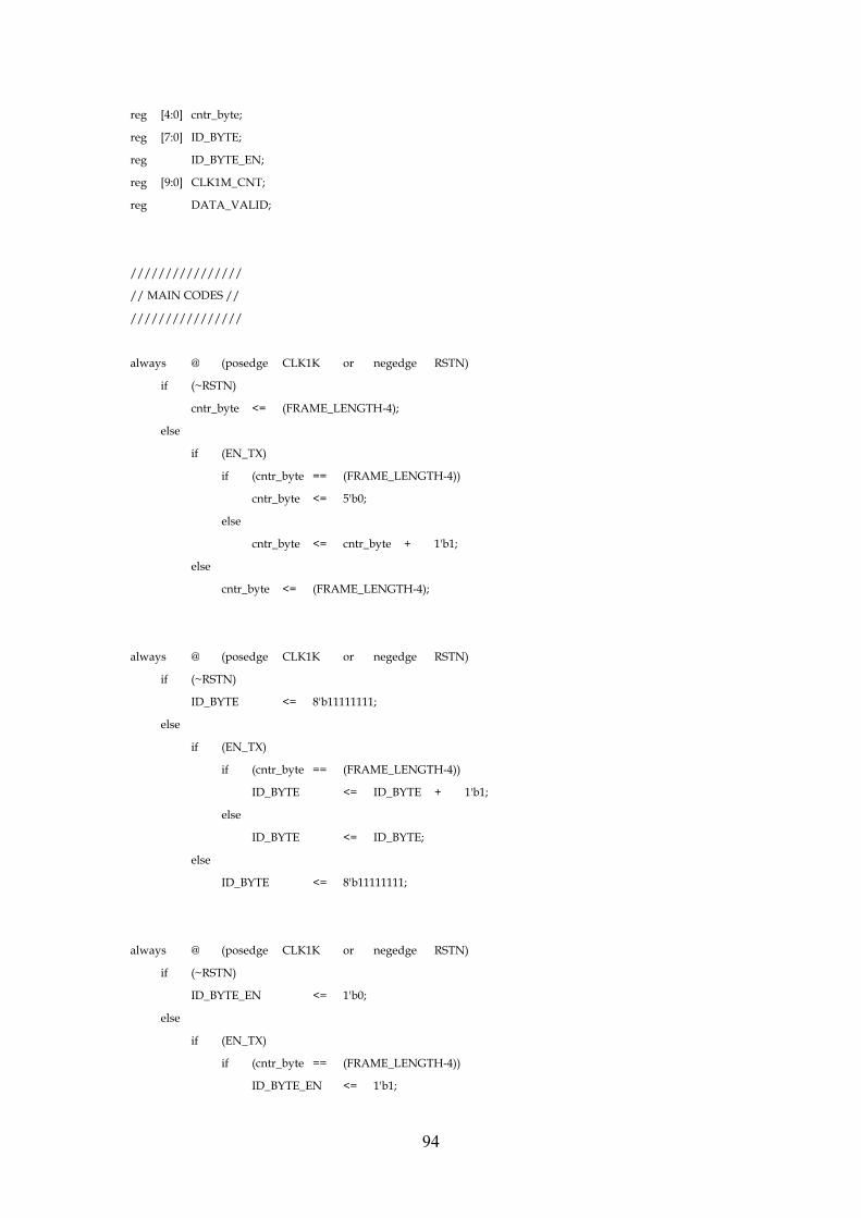
94
reg [4:0] cntr_byte;
reg [7:0] ID_BYTE;
reg ID_BYTE_EN;
reg [9:0] CLK1M_CNT;
reg DATA_VALID;
////////////////
// MAIN CODES //
////////////////
always @ (posedge CLK1K or negedge RSTN)
if (~RSTN)
cntr_byte <= (FRAME_LENGTH-4);
else
if (EN_TX)
if (cntr_byte == (FRAME_LENGTH-4))
cntr_byte <= 5'b0;
else
cntr_byte <= cntr_byte + 1'b1;
else
cntr_byte <= (FRAME_LENGTH-4);
always @ (posedge CLK1K or negedge RSTN)
if (~RSTN)
ID_BYTE <= 8'b11111111;
else
if (EN_TX)
if (cntr_byte == (FRAME_LENGTH-4))
ID_BYTE <= ID_BYTE + 1'b1;
else
ID_BYTE <= ID_BYTE;
else
ID_BYTE <= 8'b11111111;
always @ (posedge CLK1K or negedge RSTN)
if (~RSTN)
ID_BYTE_EN <= 1'b0;
else
if (EN_TX)
if (cntr_byte == (FRAME_LENGTH-4))
ID_BYTE_EN <= 1'b1;
95
else
ID_BYTE_EN <= 1'b0;
else
ID_BYTE_EN <= 1'b0;
always @ (posedge CLK1M or negedge RSTN)
if (~RSTN)
CLK1M_CNT <= 10'b1111111111;
else
if (ID_BYTE_EN)
CLK1M_CNT <= CLK1M_CNT + 1'b1;
else
CLK1M_CNT <= 10'b1111111111;
always @ (posedge CLK1M or negedge RSTN)
begin
if (~RSTN)
DATA_VALID <= 1'b0;
else
if (CLK1M_CNT == 10'b0000000010)
DATA_VALID <= 1'b1;
else
DATA_VALID <= 1'b0;
end
endmodule //BPRO_TX_BB_MAC_ID_GEN
96
Appendix C: Verilog RTL code of packet generator for transmitter
/////////////////////////////////////
// SPI_MULT_BYTE_CMD_WR SUB-MODULE //
/////////////////////////////////////
module SPI_MULT_BYTE_WR(
//input
CLK,
CLK4M,
RSTN,
CRC_ON,
CMD,
LENGTH,
FRAME,
RUN,
//output
CSN,
SO,
SCLK,
EOS
);
///////////
// INPUTS
///////////
input CLK;
input CLK4M;
input RSTN;
input CRC_ON;
input [7:0] CMD;
input [((FRAME_LENGTH-2)*8-1) : 0] FRAME;

97
input [7:0] LENGTH;
input RUN;
////////////
// OUTPUTS
////////////
output CSN;
output SO;
output SCLK;
output EOS;
////////////////////////
// SIGNAL DECLARATIONS
////////////////////////
reg [3:0] STATE;
reg EN_CMD_CNT;
reg [7:0] CMD_CNT;
reg [7:0] CMD_BYTE;
reg EN_LENGTH;
reg [7:0] LENGTH_BYTE;
reg [((FRAME_LENGTH-2)*8-1) : 0] FRAME_DATA;
reg EN_FRAME;
reg EN_CRC;
reg [15:0] CRC_R;
reg EN_CLK4M_CNT;
reg [9:0] CLK4M_CNT;
reg CSN;
reg EOS;
reg SO;

98
///////////////
// MAIN CODES
///////////////
//state transition
always @(posedge CLK or negedge RSTN)
begin
if (~RSTN)
STATE <= RST_STATE;
else
begin
case (STATE)
RST_STATE: begin
STATE <= CHK_RUN;
end
CHK_RUN: begin
if (RUN == 1'b1)
STATE <= SEND_CMD;
else
STATE <= CHK_RUN;
end
SEND_CMD: begin
if (CMD_CNT == 7)
STATE <= SEND_LENGTH;
else
STATE <= SEND_CMD;
end
SEND_LENGTH: begin
if (CMD_CNT == 15)
STATE <= SEND_FRAME;
else
STATE <= SEND_LENGTH;
end
SEND_FRAME: begin
//if (CMD_CNT == ((SPI_DATA_OUT_MAX_BYTE-2)*8 + 7))
if (CMD_CNT == ((FRAME_LENGTH-2)*8 + 15))
STATE <= SEND_CRC;
else
STATE <= SEND_FRAME;
99
end
SEND_CRC: begin
//if (CMD_CNT == (SPI_DATA_OUT_MAX_BYTE*8 + 7))
if (CMD_CNT == ((FRAME_LENGTH)*8 + 15))
STATE <= CMD_END;
else
STATE <= SEND_CRC;
end
CMD_END: begin
STATE <= RUN_END;
end
RUN_END: begin
STATE <= CHK_RUN;
end
default: begin
STATE <= RST_STATE;
end
endcase
end
end //state transition
//output assignment
always @(*)
begin
case (STATE)
RST_STATE: begin
EN_CMD_CNT <= 1'b0;
EN_LENGTH <= 1'b0;
EN_FRAME <= 1'b0;
EN_CRC <= 1'b0;
EN_CLK4M_CNT <= 1'b0;
EOS <= 1'b0;
end
CHK_RUN: begin
EN_CMD_CNT <= 1'b0;
EN_LENGTH <= 1'b0;
EN_FRAME <= 1'b0;
EN_CRC <= 1'b0;

100
EN_CLK4M_CNT <= 1'b0;
EOS <= 1'b0;
end
SEND_CMD: begin
EN_CMD_CNT <= 1'b1;
EN_LENGTH <= 1'b0;
EN_FRAME <= 1'b0;
EN_CRC <= 1'b0;
EN_CLK4M_CNT <= 1'b1;
EOS <= 1'b0;
end
SEND_LENGTH: begin
EN_CMD_CNT <= 1'b1;
EN_LENGTH <= 1'b1;
EN_FRAME <= 1'b0;
EN_CRC <= 1'b0;
EN_CLK4M_CNT <= 1'b1;
EOS <= 1'b0;
end
SEND_FRAME: begin
EN_CMD_CNT <= 1'b1;
EN_LENGTH <= 1'b1;
EN_FRAME <= 1'b1;
EN_CRC <= 1'b0;
EN_CLK4M_CNT <= 1'b1;
EOS <= 1'b0;
end
SEND_CRC: begin
EN_CMD_CNT <= 1'b1;
EN_LENGTH <= 1'b1;
EN_FRAME <= 1'b1;
EN_CRC <= 1'b1;
EN_CLK4M_CNT <= 1'b1;
EOS <= 1'b0;
end
CMD_END: begin
EN_CMD_CNT <= 1'b0;
EN_LENGTH <= 1'b0;

101
EN_FRAME <= 1'b0;
EN_CRC <= 1'b0;
EN_CLK4M_CNT <= 1'b1;
EOS <= 1'b1;
end
RUN_END: begin
EN_CMD_CNT <= 1'b0;
EN_LENGTH <= 1'b0;
EN_FRAME <= 1'b0;
EN_CRC <= 1'b0;
EN_CLK4M_CNT <= 1'b0;
EOS <= 1'b0;
end
default: begin
EN_CMD_CNT <= 1'b0;
EN_LENGTH <= 1'b0;
EN_FRAME <= 1'b0;
EN_CRC <= 1'b0;
EN_CLK4M_CNT <= 1'b0;
EOS <= 1'b0;
end
endcase
end //output assignment
//command byte CMD_BYTE shift out and generate command bit counter CMD_CNT
always @(posedge CLK or negedge RSTN)
begin
if (~RSTN)
begin
CMD_BYTE <= 0;
LENGTH_BYTE <= 0;
FRAME_DATA <= 0;
CMD_CNT <= 0;
end
else if (RUN == 1'b1)
begin
CMD_BYTE <= CMD;
LENGTH_BYTE <= LENGTH;
FRAME_DATA <= FRAME;
CMD_CNT <= 0;
end
else
102
begin
if (EN_CMD_CNT==1'b1)
begin
if (EN_LENGTH == 1'b1)
begin
if (EN_FRAME == 1'b1)
begin
CMD_BYTE <= CMD_BYTE;
LENGTH_BYTE <= LENGTH_BYTE;
FRAME_DATA <= {1'b0, FRAME_DATA[((FRAME_LENGTH-2)*8 - 1):1]};
CMD_CNT <= CMD_CNT + 1;
end
else
begin
CMD_BYTE <= CMD_BYTE;
LENGTH_BYTE <= {1'b0, LENGTH_BYTE[7:1]};
FRAME_DATA <= FRAME_DATA;
CMD_CNT <= CMD_CNT + 1;
end
end
else
begin
CMD_BYTE <= {CMD_BYTE[6:0], 1'b0};
LENGTH_BYTE <= LENGTH_BYTE;
FRAME_DATA <= FRAME_DATA;
CMD_CNT <= CMD_CNT + 1;
end
end
else
begin
CMD_BYTE <= CMD_BYTE;
LENGTH_BYTE <= LENGTH_BYTE;
FRAME_DATA <= FRAME_DATA;
CMD_CNT <= CMD_CNT;
end
end
end
//command byte shift out and generate command bit counter
//generate 4MHz clock counter CLK4M_CNT
always @(posedge CLK4M or negedge RSTN)
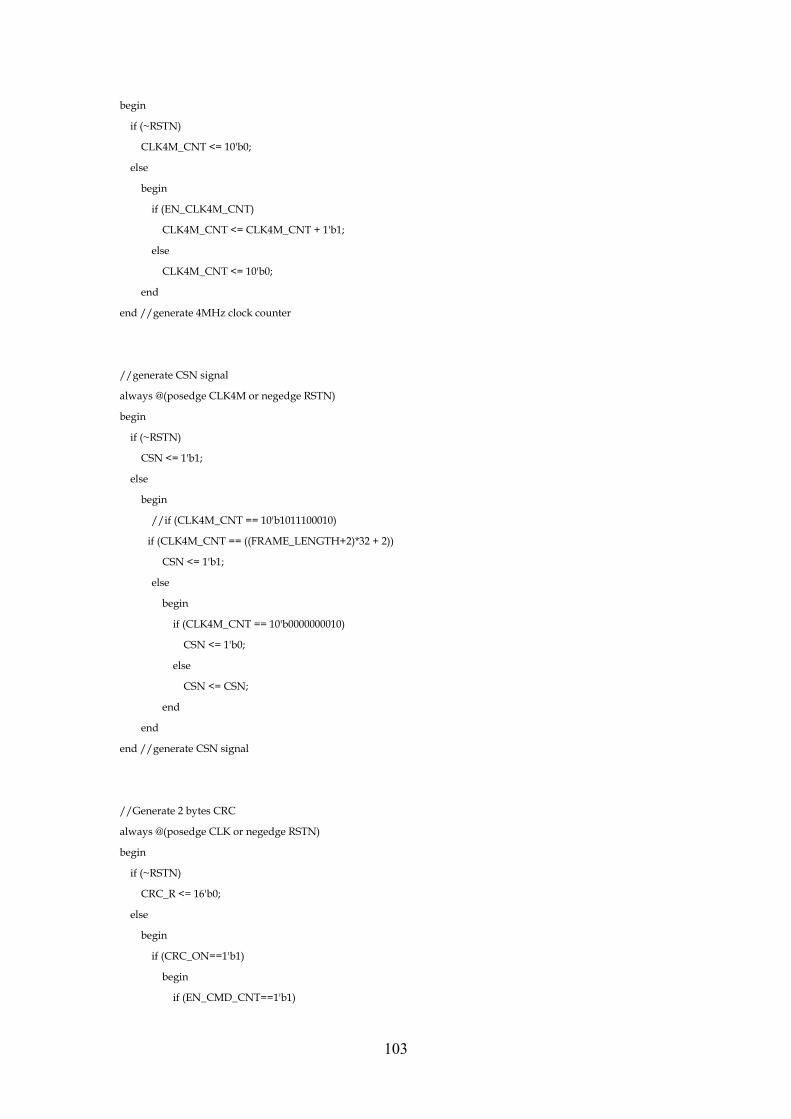
103
begin
if (~RSTN)
CLK4M_CNT <= 10'b0;
else
begin
if (EN_CLK4M_CNT)
CLK4M_CNT <= CLK4M_CNT + 1'b1;
else
CLK4M_CNT <= 10'b0;
end
end //generate 4MHz clock counter
//generate CSN signal
always @(posedge CLK4M or negedge RSTN)
begin
if (~RSTN)
CSN <= 1'b1;
else
begin
//if (CLK4M_CNT == 10'b1011100010)
if (CLK4M_CNT == ((FRAME_LENGTH+2)*32 + 2))
CSN <= 1'b1;
else
begin
if (CLK4M_CNT == 10'b0000000010)
CSN <= 1'b0;
else
CSN <= CSN;
end
end
end //generate CSN signal
//Generate 2 bytes CRC
always @(posedge CLK or negedge RSTN)
begin
if (~RSTN)
CRC_R <= 16'b0;
else
begin
if (CRC_ON==1'b1)
begin
if (EN_CMD_CNT==1'b1)
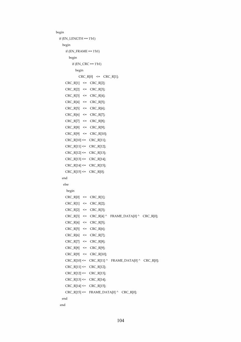
104
begin
if (EN_LENGTH == 1'b1)
begin
if (EN_FRAME == 1'b1)
begin
if (EN_CRC == 1'b1)
begin
CRC_R[0] <= CRC_R[1];
CRC_R[1] <= CRC_R[2];
CRC_R[2] <= CRC_R[3];
CRC_R[3] <= CRC_R[4];
CRC_R[4] <= CRC_R[5];
CRC_R[5] <= CRC_R[6];
CRC_R[6] <= CRC_R[7];
CRC_R[7] <= CRC_R[8];
CRC_R[8] <= CRC_R[9];
CRC_R[9] <= CRC_R[10];
CRC_R[10] <= CRC_R[11];
CRC_R[11] <= CRC_R[12];
CRC_R[12] <= CRC_R[13];
CRC_R[13] <= CRC_R[14];
CRC_R[14] <= CRC_R[15];
CRC_R[15] <= CRC_R[0];
end
else
begin
CRC_R[0] <= CRC_R[1];
CRC_R[1] <= CRC_R[2];
CRC_R[2] <= CRC_R[3];
CRC_R[3] <= CRC_R[4] ^ FRAME_DATA[0] ^ CRC_R[0];
CRC_R[4] <= CRC_R[5];
CRC_R[5] <= CRC_R[6];
CRC_R[6] <= CRC_R[7];
CRC_R[7] <= CRC_R[8];
CRC_R[8] <= CRC_R[9];
CRC_R[9] <= CRC_R[10];
CRC_R[10] <= CRC_R[11] ^ FRAME_DATA[0] ^ CRC_R[0];
CRC_R[11] <= CRC_R[12];
CRC_R[12] <= CRC_R[13];
CRC_R[13] <= CRC_R[14];
CRC_R[14] <= CRC_R[15];
CRC_R[15] <= FRAME_DATA[0] ^ CRC_R[0];
end
end

105
else
CRC_R <= 16'b0;
end
else
CRC_R <= 16'b0;
end
else
CRC_R <= 16'b0;
end
else
CRC_R <= 16'b0;
end
end //Generate 2 bytes CRC
//generate output signal SO, delay half CLK, negedge change
always @(negedge CLK or negedge RSTN)
begin
if (~RSTN)
SO <= 1'b0;
else
begin
if (EN_CMD_CNT==1'b1)
begin
if (EN_LENGTH == 1'b1)
begin
if (EN_FRAME == 1'b1)
begin
if (EN_CRC == 1'b1)
SO <= CRC_R[0];
else
SO <= FRAME_DATA[0];
end
else
SO <= LENGTH_BYTE[0];
end
else
SO <= CMD_BYTE[7];
end
else
SO <= 1'b0;
end
end //generate output signal SO

106
assign SCLK = ~CSN & CLK;
endmodule //SPI_MULT_BYTE_WR

107
Appendix D: Verilog RTL code of microcontroller for transmitter
////////////////
// TOP MODULE
////////////////
module BPRO_TX_BB_MAC_SPI_SM(
//input
MAC_SPI_SM_CLK,
MAC_SPI_SM_RSTN,
MAC_SPI_SM_EOS,
MAC_SPI_SM_EN_TX, // control TX_ON time
MAC_SPI_SM_PHY_REG,
MAC_SPI_SM_VALID_PHY_REG,
MAC_SPI_SM_DATA_VALID,
//output
MAC_SPI_SM_SOS,
MAC_SPI_SM_CMD_CODE,
MAC_SPI_SM_CMD_RW,
MAC_SPI_SM_CMD_TYPE,
MAC_SPI_SM_DATA
);
///////////////
// PARAMETERS
///////////////
//SPI command codes
parameter [6:0] PLL500kHzON = 7'b0100100,
PA_CTRL_Tx = 7'b0010000,
ModHighInitTx = 7'b0100001,
ModLowInitTX = 7'b0100000,
PS_CTRL_TX = 7'b0100010,
PLLPD_TX = 7'b0100011,
FracN_MID = 7'b0100110,
BB_CTRL = 7'b0000111,
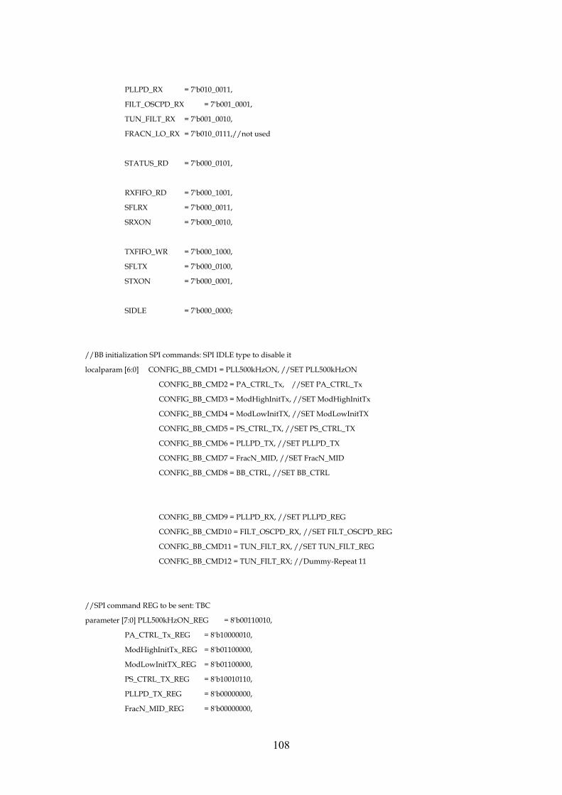
108
PLLPD_RX = 7'b010_0011,
FILT_OSCPD_RX = 7'b001_0001,
TUN_FILT_RX = 7'b001_0010,
FRACN_LO_RX = 7'b010_0111,//not used
STATUS_RD = 7'b000_0101,
RXFIFO_RD = 7'b000_1001,
SFLRX = 7'b000_0011,
SRXON = 7'b000_0010,
TXFIFO_WR = 7'b000_1000,
SFLTX = 7'b000_0100,
STXON = 7'b000_0001,
SIDLE = 7'b000_0000;
//BB initialization SPI commands: SPI IDLE type to disable it
localparam [6:0] CONFIG_BB_CMD1 = PLL500kHzON, //SET PLL500kHzON
CONFIG_BB_CMD2 = PA_CTRL_Tx, //SET PA_CTRL_Tx
CONFIG_BB_CMD3 = ModHighInitTx, //SET ModHighInitTx
CONFIG_BB_CMD4 = ModLowInitTX, //SET ModLowInitTX
CONFIG_BB_CMD5 = PS_CTRL_TX, //SET PS_CTRL_TX
CONFIG_BB_CMD6 = PLLPD_TX, //SET PLLPD_TX
CONFIG_BB_CMD7 = FracN_MID, //SET FracN_MID
CONFIG_BB_CMD8 = BB_CTRL, //SET BB_CTRL
CONFIG_BB_CMD9 = PLLPD_RX, //SET PLLPD_REG
CONFIG_BB_CMD10 = FILT_OSCPD_RX, //SET FILT_OSCPD_REG
CONFIG_BB_CMD11 = TUN_FILT_RX, //SET TUN_FILT_REG
CONFIG_BB_CMD12 = TUN_FILT_RX; //Dummy-Repeat 11
//SPI command REG to be sent: TBC
parameter [7:0] PLL500kHzON_REG = 8'b00110010,
PA_CTRL_Tx_REG = 8'b10000010,
ModHighInitTx_REG = 8'b01100000,
ModLowInitTX_REG = 8'b01100000,
PS_CTRL_TX_REG = 8'b10010110,
PLLPD_TX_REG = 8'b00000000,
FracN_MID_REG = 8'b00000000,
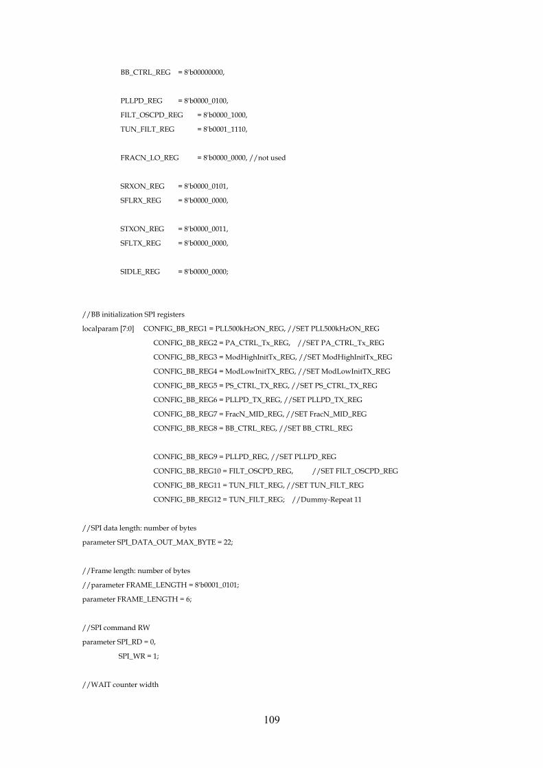
109
BB_CTRL_REG = 8'b00000000,
PLLPD_REG = 8'b0000_0100,
FILT_OSCPD_REG = 8'b0000_1000,
TUN_FILT_REG = 8'b0001_1110,
FRACN_LO_REG = 8'b0000_0000, //not used
SRXON_REG = 8'b0000_0101,
SFLRX_REG = 8'b0000_0000,
STXON_REG = 8'b0000_0011,
SFLTX_REG = 8'b0000_0000,
SIDLE_REG = 8'b0000_0000;
//BB initialization SPI registers
localparam [7:0] CONFIG_BB_REG1 = PLL500kHzON_REG, //SET PLL500kHzON_REG
CONFIG_BB_REG2 = PA_CTRL_Tx_REG, //SET PA_CTRL_Tx_REG
CONFIG_BB_REG3 = ModHighInitTx_REG, //SET ModHighInitTx_REG
CONFIG_BB_REG4 = ModLowInitTX_REG, //SET ModLowInitTX_REG
CONFIG_BB_REG5 = PS_CTRL_TX_REG, //SET PS_CTRL_TX_REG
CONFIG_BB_REG6 = PLLPD_TX_REG, //SET PLLPD_TX_REG
CONFIG_BB_REG7 = FracN_MID_REG, //SET FracN_MID_REG
CONFIG_BB_REG8 = BB_CTRL_REG, //SET BB_CTRL_REG
CONFIG_BB_REG9 = PLLPD_REG, //SET PLLPD_REG
CONFIG_BB_REG10 = FILT_OSCPD_REG, //SET FILT_OSCPD_REG
CONFIG_BB_REG11 = TUN_FILT_REG, //SET TUN_FILT_REG
CONFIG_BB_REG12 = TUN_FILT_REG; //Dummy-Repeat 11
//SPI data length: number of bytes
parameter SPI_DATA_OUT_MAX_BYTE = 22;
//Frame length: number of bytes
//parameter FRAME_LENGTH = 8'b0001_0101;
parameter FRAME_LENGTH = 6;
//SPI command RW
parameter SPI_RD = 0,
SPI_WR = 1;
//WAIT counter width
110
parameter WAIT_CNT_W = 4;
//WAIT length
parameter [3:0] WAIT_CYCLES = 4'b1111;
//STXON WAIT length
parameter STXON_WAIT_CYCLES = (FRAME_LENGTH + 4 + 1 + 1)*8*6; //6: 4 * 1.5, 1.5: 1 + 0.33 => 1.5
//SPI command types
parameter [2:0] SPI_IDLE = 0, //DO NOTHING
SPI_ONE_BYTE_CMD = 1, //ALWAYS WR
SPI_TWO_BYTE_WR = 2,
SPI_TWO_BYTE_RD = 3,
SPI_MULT_BYTE_RD = 4,
SPI_MULT_BYTE_WR = 5;
//state machine states
parameter [5:0] RST_STATE = 0,
CONFIG_BB1 = 1, //SET PLL500kHzON
WAIT1 = 2,
CONFIG_BB2 = 3, //SET PA_CTRL_Tx
WAIT2 = 4,
CONFIG_BB3 = 5, //SET ModHighInitTx
WAIT3 = 6,
CONFIG_BB4 = 7, //SET ModLowInitTX
WAIT4 = 8,
CONFIG_BB5 = 9, //SET PS_CTRL_TX
WAIT5 = 10,
CONFIG_BB6 = 11, //SET PLLPD_TX
WAIT6 = 12,
CONFIG_BB7 = 13, //SET FracN_MID
WAIT7 = 14,
CONFIG_BB8 = 15, //SET BB_CTRL
WAIT8 = 16,
POLL_DATA = 17,
RD_STATUS_REG1 = 18,
CK_TXFIFO_STATUS1 = 19,
FLUSH_TXFIFO = 20,
RD_STATUS_REG2 = 21,
CK_TXFIFO_STATUS2 = 22,
WR_FRAME = 23,
RD_STATUS_REG3 = 24,
CK_TXFIFO_STATUS3 = 25,

111
SET_STXON = 26,
RD_STATUS_REG4 = 27,
CK_TXFIFO_STATUS4 = 28,
CNTR_STXON = 29;
/*
CONFIG_BB9 = 17, //SET PLLPD_REG
WAIT9 = 18,
CONFIG_BB10 = 19, //SET FILT_OSCPD_REG
WAIT10 = 20,
CONFIG_BB11 = 21, //SET TUN_FILT_REG
WAIT11 = 22,
CONFIG_BB12 = 23, //Dummy-Repeat 11
WAIT12 = 24,
POLL_IRQ = 25,
RD_STATUS_REG1 = 26,
CK_RXFIFO_STATUS1 = 27,
RD_FRAME = 28,
RD_STATUS_REG2 = 29,
CK_RXFIFO_STATUS2 = 30,
FLUSH_RXFIFO = 31,
RD_STATUS_REG3 = 32,
CK_RXFIFO_STATUS3 = 33,
SET_SRXON = 34,
SET_SIDLE1 = 35,
SET_SIDLE2 = 36;
*/
///////////
// INPUTS
///////////
input MAC_SPI_SM_CLK;
input MAC_SPI_SM_RSTN;
input MAC_SPI_SM_EN_TX;
input MAC_SPI_SM_EOS;
input MAC_SPI_SM_VALID_PHY_REG;
input [7:0] MAC_SPI_SM_PHY_REG;

112
input MAC_SPI_SM_DATA_VALID;
////////////
// OUTPUTS
////////////
output MAC_SPI_SM_SOS;
output [6:0] MAC_SPI_SM_CMD_CODE;
output MAC_SPI_SM_CMD_RW;
output [2:0] MAC_SPI_SM_CMD_TYPE;
//output RST_PHY;
output [7:0] MAC_SPI_SM_DATA;
//output MAC_RX_BUSY;
////////////
// INOUTS
////////////
////////////////////////
// SIGNAL DECLARATIONS
////////////////////////
reg [5:0] MAC_SPI_STATE;
reg [5:0] MAC_SPI_STATE_D1;
//reg RST_PHY;
reg [WAIT_CNT_W-1:0] CONFIG_WAIT_CNT;
reg WAIT_CNT_EN;
//wire WAIT_CNT_FULL;
//reg MAC_SPI_CMD_EN;
//reg MAC_SPI_CMD_EN_D1;
reg [6:0] MAC_SPI_SM_CMD_CODE;
//reg [6:0] MAC_SPI_SM_CMD_CODE_D1;
reg MAC_SPI_SM_CMD_RW;
reg [2:0] MAC_SPI_SM_CMD_TYPE;
113
//reg [2:0] MAC_SPI_SM_CMD_TYPE_D1;
reg [7 : 0] MAC_SPI_SM_DATA;
//reg MAC_RX_BUSY;
reg STXON_WAIT_CNT_EN;
reg [10:0] STXON_WAIT_CNT;
///////////////
// MAIN CODES
///////////////
//start of SPI generation
always @(posedge MAC_SPI_SM_CLK or negedge MAC_SPI_SM_RSTN)
begin
if (~MAC_SPI_SM_RSTN) begin
MAC_SPI_STATE_D1 <= 0;
//MAC_SPI_SM_CMD_TYPE_D1 <= 0;
end
else begin
MAC_SPI_STATE_D1 <= MAC_SPI_STATE;
//MAC_SPI_SM_CMD_TYPE_D1 <= MAC_SPI_SM_CMD_TYPE;
end
end
//state change generates a SOS pulse
assign MAC_SPI_SM_SOS = (MAC_SPI_STATE == MAC_SPI_STATE_D1)? 1'b0 :
(MAC_SPI_SM_CMD_TYPE == SPI_IDLE)? 1'b0: 1'b1; //TBC
//state transition
always @(posedge MAC_SPI_SM_CLK or negedge MAC_SPI_SM_RSTN)
begin
if (~MAC_SPI_SM_RSTN)
MAC_SPI_STATE <= RST_STATE;
else
begin
if (MAC_SPI_SM_DATA_VALID)
MAC_SPI_STATE <= RD_STATUS_REG1;
else
case (MAC_SPI_STATE)
RST_STATE: begin
MAC_SPI_STATE <= CONFIG_BB1;

114
end
////////////////////////////
//BB RF&PHY initialization
////////////////////////////
//SET BB REG1
CONFIG_BB1: begin
if (MAC_SPI_SM_EOS == 1'b1)
MAC_SPI_STATE <= WAIT1;
else
MAC_SPI_STATE <= CONFIG_BB1;
end
WAIT1: begin
if (CONFIG_WAIT_CNT == WAIT_CYCLES)
MAC_SPI_STATE <= CONFIG_BB2;
else
MAC_SPI_STATE <= WAIT1;
end
//SET BB REG2
CONFIG_BB2: begin
if (MAC_SPI_SM_EOS == 1'b1)
MAC_SPI_STATE <= WAIT2;
else
MAC_SPI_STATE <= CONFIG_BB2;
end
WAIT2: begin
if (CONFIG_WAIT_CNT == WAIT_CYCLES)
MAC_SPI_STATE <= CONFIG_BB3;
else
MAC_SPI_STATE <= WAIT2;
end
//SET BB REG3
CONFIG_BB3: begin
if (MAC_SPI_SM_EOS == 1'b1)
MAC_SPI_STATE <= WAIT3;
else
MAC_SPI_STATE <= CONFIG_BB3;
end

115
WAIT3: begin
if (CONFIG_WAIT_CNT == WAIT_CYCLES)
MAC_SPI_STATE <= CONFIG_BB4;
else
MAC_SPI_STATE <= WAIT3;
end
//SET BB REG4
CONFIG_BB4: begin
if (MAC_SPI_SM_EOS == 1'b1)
MAC_SPI_STATE <= WAIT4;
else
MAC_SPI_STATE <= CONFIG_BB4;
end
WAIT4: begin
if (CONFIG_WAIT_CNT == WAIT_CYCLES)
MAC_SPI_STATE <= CONFIG_BB5;
else
MAC_SPI_STATE <= WAIT4;
end
//SET BB REG5
CONFIG_BB5: begin
if (MAC_SPI_SM_EOS == 1'b1)
MAC_SPI_STATE <= WAIT5;
else
MAC_SPI_STATE <= CONFIG_BB5;
end
WAIT5: begin
if (CONFIG_WAIT_CNT == WAIT_CYCLES)
MAC_SPI_STATE <= CONFIG_BB6;
else
MAC_SPI_STATE <= WAIT5;
end
//SET BB REG6
CONFIG_BB6: begin
if (MAC_SPI_SM_EOS == 1'b1)
MAC_SPI_STATE <= WAIT6;
else
MAC_SPI_STATE <= CONFIG_BB6;
end

116
WAIT6: begin
if (CONFIG_WAIT_CNT == WAIT_CYCLES)
MAC_SPI_STATE <= CONFIG_BB7;
else
MAC_SPI_STATE <= WAIT6;
end
//SET BB REG7
CONFIG_BB7: begin
if (MAC_SPI_SM_EOS == 1'b1)
MAC_SPI_STATE <= WAIT7;
else
MAC_SPI_STATE <= CONFIG_BB7;
end
WAIT7: begin
if (CONFIG_WAIT_CNT == WAIT_CYCLES)
MAC_SPI_STATE <= CONFIG_BB8;
else
MAC_SPI_STATE <= WAIT7;
end
//SET BB REG8
CONFIG_BB8: begin
if (MAC_SPI_SM_EOS == 1'b1)
MAC_SPI_STATE <= WAIT8;
else
MAC_SPI_STATE <= CONFIG_BB8;
end
WAIT8: begin
if (CONFIG_WAIT_CNT == WAIT_CYCLES)
MAC_SPI_STATE <= POLL_DATA;
else
MAC_SPI_STATE <= WAIT8;
end
///////////////////
// END OF BB INIT
///////////////////
//Poll Data valid bit

117
POLL_DATA: begin
if (MAC_SPI_SM_DATA_VALID == 1'b1)
MAC_SPI_STATE <= RD_STATUS_REG1;
else
MAC_SPI_STATE <= POLL_DATA;
end
//RD_STATUS_REG1
RD_STATUS_REG1: begin
if (MAC_SPI_SM_VALID_PHY_REG == 1'b1)
MAC_SPI_STATE <= CK_TXFIFO_STATUS1;
else
MAC_SPI_STATE <= RD_STATUS_REG1;
end
//CK_TXFIFO_STATUS1
CK_TXFIFO_STATUS1: begin
if (MAC_SPI_SM_PHY_REG[0] == 1'b1)
MAC_SPI_STATE <= FLUSH_TXFIFO;
else
MAC_SPI_STATE <= RD_STATUS_REG1;
end
//FLUSH_TXFIFO
FLUSH_TXFIFO: begin
if (MAC_SPI_SM_EOS == 1'b1)
MAC_SPI_STATE <= RD_STATUS_REG2;
else
MAC_SPI_STATE <= FLUSH_TXFIFO;
end
//RD_STATUS_REG2
RD_STATUS_REG2: begin
if (MAC_SPI_SM_VALID_PHY_REG == 1'b1)
MAC_SPI_STATE <= CK_TXFIFO_STATUS2;
else
MAC_SPI_STATE <= RD_STATUS_REG2;
end
//CK_TXFIFO_STATUS2
CK_TXFIFO_STATUS2: begin
if ((MAC_SPI_SM_PHY_REG[2] == 1'b0) && (MAC_SPI_SM_PHY_REG[0] == 1'b1))
MAC_SPI_STATE <= WR_FRAME;
else //wait to Flush again
118
MAC_SPI_STATE <= RD_STATUS_REG1;
end
//WR_FIFO_FRAME
WR_FRAME: begin
if (MAC_SPI_SM_EOS == 1'b1)
MAC_SPI_STATE <= RD_STATUS_REG3;
else
MAC_SPI_STATE <= WR_FRAME;
end
//RD_STATUS_REG3
RD_STATUS_REG3: begin
if (MAC_SPI_SM_VALID_PHY_REG == 1'b1)
MAC_SPI_STATE <= CK_TXFIFO_STATUS3;
else
MAC_SPI_STATE <= RD_STATUS_REG3;
end
//CK_TXFIFO_STATUS3
CK_TXFIFO_STATUS3: begin
if (MAC_SPI_SM_PHY_REG[2] == 1'b1)
MAC_SPI_STATE <= SET_STXON;
else //wait to Flush again
MAC_SPI_STATE <= RD_STATUS_REG2;
end
SET_STXON: begin
if (MAC_SPI_SM_EOS == 1'b1)
MAC_SPI_STATE <= RD_STATUS_REG4;
else
MAC_SPI_STATE <= SET_STXON;
end
//RD_STATUS_REG4
RD_STATUS_REG4: begin
if (MAC_SPI_SM_VALID_PHY_REG == 1'b1)
MAC_SPI_STATE <= CK_TXFIFO_STATUS4;
else
MAC_SPI_STATE <= RD_STATUS_REG4;
end
//CK_TXFIFO_STATUS4
CK_TXFIFO_STATUS4: begin

119
if (MAC_SPI_SM_PHY_REG[0] == 1'b0)
MAC_SPI_STATE <= CNTR_STXON;
else
MAC_SPI_STATE <= SET_STXON;
end
CNTR_STXON: begin
if (STXON_WAIT_CNT == STXON_WAIT_CYCLES)
MAC_SPI_STATE <= SET_STXON;
else
MAC_SPI_STATE <= CNTR_STXON;
end
default: begin
MAC_SPI_STATE <= RST_STATE;
end
endcase
end
end //state transition
//output assignment
always @(*)
begin
case (MAC_SPI_STATE)
RST_STATE: begin
MAC_SPI_SM_CMD_CODE <= 7'b000_0000;
MAC_SPI_SM_CMD_RW <= 1'b0;
MAC_SPI_SM_CMD_TYPE <= 3'b000;
MAC_SPI_SM_DATA <= 8'b0000_0000;
//RST_PHY <= 1'b1;
STXON_WAIT_CNT_EN <= 1'b0;
WAIT_CNT_EN <= 1'b0;
end
///////////////////////////
//BB RF&PHY initialization
///////////////////////////
//SET BB REG1
CONFIG_BB1: begin
MAC_SPI_SM_CMD_CODE <= CONFIG_BB_CMD1;
120
MAC_SPI_SM_CMD_RW <= SPI_WR;
MAC_SPI_SM_CMD_TYPE <= SPI_TWO_BYTE_WR;
MAC_SPI_SM_DATA <= CONFIG_BB_REG1;
//RST_PHY <= 1'b1;
STXON_WAIT_CNT_EN <= 1'b0;
WAIT_CNT_EN <= 1'b0;
end
WAIT1: begin
MAC_SPI_SM_CMD_CODE <= 7'b000_0000;
MAC_SPI_SM_CMD_RW <= 1'b0;
MAC_SPI_SM_CMD_TYPE <= SPI_IDLE;
MAC_SPI_SM_DATA <= 8'b0000_0000;
//RST_PHY <= 1'b1;
STXON_WAIT_CNT_EN <= 1'b0;
WAIT_CNT_EN <= 1'b1;
end
//SET BB REG2
CONFIG_BB2: begin
MAC_SPI_SM_CMD_CODE <= CONFIG_BB_CMD2;
MAC_SPI_SM_CMD_RW <= SPI_WR;
MAC_SPI_SM_CMD_TYPE <= SPI_TWO_BYTE_WR;
MAC_SPI_SM_DATA <= CONFIG_BB_REG2;
//RST_PHY <= 1'b1;
STXON_WAIT_CNT_EN <= 1'b0;
WAIT_CNT_EN <= 1'b0;
end
WAIT2: begin
MAC_SPI_SM_CMD_CODE <= 7'b000_0000;
MAC_SPI_SM_CMD_RW <= 1'b0;
MAC_SPI_SM_CMD_TYPE <= SPI_IDLE;
MAC_SPI_SM_DATA <= 8'b0000_0000;
//RST_PHY <= 1'b1;
STXON_WAIT_CNT_EN <= 1'b0;
WAIT_CNT_EN <= 1'b1;
end
//SET BB REG3
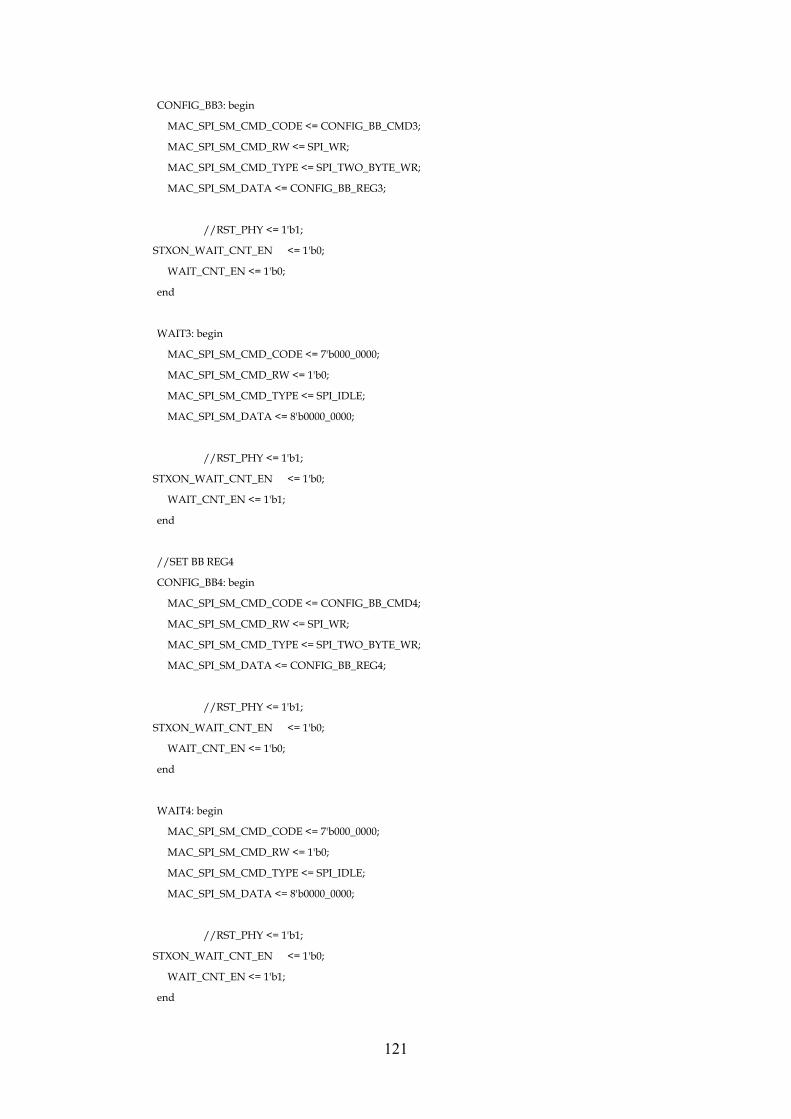
121
CONFIG_BB3: begin
MAC_SPI_SM_CMD_CODE <= CONFIG_BB_CMD3;
MAC_SPI_SM_CMD_RW <= SPI_WR;
MAC_SPI_SM_CMD_TYPE <= SPI_TWO_BYTE_WR;
MAC_SPI_SM_DATA <= CONFIG_BB_REG3;
//RST_PHY <= 1'b1;
STXON_WAIT_CNT_EN <= 1'b0;
WAIT_CNT_EN <= 1'b0;
end
WAIT3: begin
MAC_SPI_SM_CMD_CODE <= 7'b000_0000;
MAC_SPI_SM_CMD_RW <= 1'b0;
MAC_SPI_SM_CMD_TYPE <= SPI_IDLE;
MAC_SPI_SM_DATA <= 8'b0000_0000;
//RST_PHY <= 1'b1;
STXON_WAIT_CNT_EN <= 1'b0;
WAIT_CNT_EN <= 1'b1;
end
//SET BB REG4
CONFIG_BB4: begin
MAC_SPI_SM_CMD_CODE <= CONFIG_BB_CMD4;
MAC_SPI_SM_CMD_RW <= SPI_WR;
MAC_SPI_SM_CMD_TYPE <= SPI_TWO_BYTE_WR;
MAC_SPI_SM_DATA <= CONFIG_BB_REG4;
//RST_PHY <= 1'b1;
STXON_WAIT_CNT_EN <= 1'b0;
WAIT_CNT_EN <= 1'b0;
end
WAIT4: begin
MAC_SPI_SM_CMD_CODE <= 7'b000_0000;
MAC_SPI_SM_CMD_RW <= 1'b0;
MAC_SPI_SM_CMD_TYPE <= SPI_IDLE;
MAC_SPI_SM_DATA <= 8'b0000_0000;
//RST_PHY <= 1'b1;
STXON_WAIT_CNT_EN <= 1'b0;
WAIT_CNT_EN <= 1'b1;
end

122
//SET BB REG5
CONFIG_BB5: begin
MAC_SPI_SM_CMD_CODE <= CONFIG_BB_CMD5;
MAC_SPI_SM_CMD_RW <= SPI_WR;
MAC_SPI_SM_CMD_TYPE <= SPI_TWO_BYTE_WR;
MAC_SPI_SM_DATA <= CONFIG_BB_REG5;
//RST_PHY <= 1'b1;
STXON_WAIT_CNT_EN <= 1'b0;
WAIT_CNT_EN <= 1'b0;
end
WAIT5: begin
MAC_SPI_SM_CMD_CODE <= 7'b000_0000;
MAC_SPI_SM_CMD_RW <= 1'b0;
MAC_SPI_SM_CMD_TYPE <= SPI_IDLE;
MAC_SPI_SM_DATA <= 8'b0000_0000;
//RST_PHY <= 1'b1;
STXON_WAIT_CNT_EN <= 1'b0;
WAIT_CNT_EN <= 1'b1;
end
//SET BB REG6
CONFIG_BB6: begin
MAC_SPI_SM_CMD_CODE <= CONFIG_BB_CMD6;
MAC_SPI_SM_CMD_RW <= SPI_WR;
MAC_SPI_SM_CMD_TYPE <= SPI_TWO_BYTE_WR;
MAC_SPI_SM_DATA <= CONFIG_BB_REG6;
//RST_PHY <= 1'b1;
STXON_WAIT_CNT_EN <= 1'b0;
WAIT_CNT_EN <= 1'b0;
end
WAIT6: begin
MAC_SPI_SM_CMD_CODE <= 7'b000_0000;
MAC_SPI_SM_CMD_RW <= 1'b0;
MAC_SPI_SM_CMD_TYPE <= SPI_IDLE;
MAC_SPI_SM_DATA <= 8'b0000_0000;
STXON_WAIT_CNT_EN <= 1'b0;
WAIT_CNT_EN <= 1'b1;
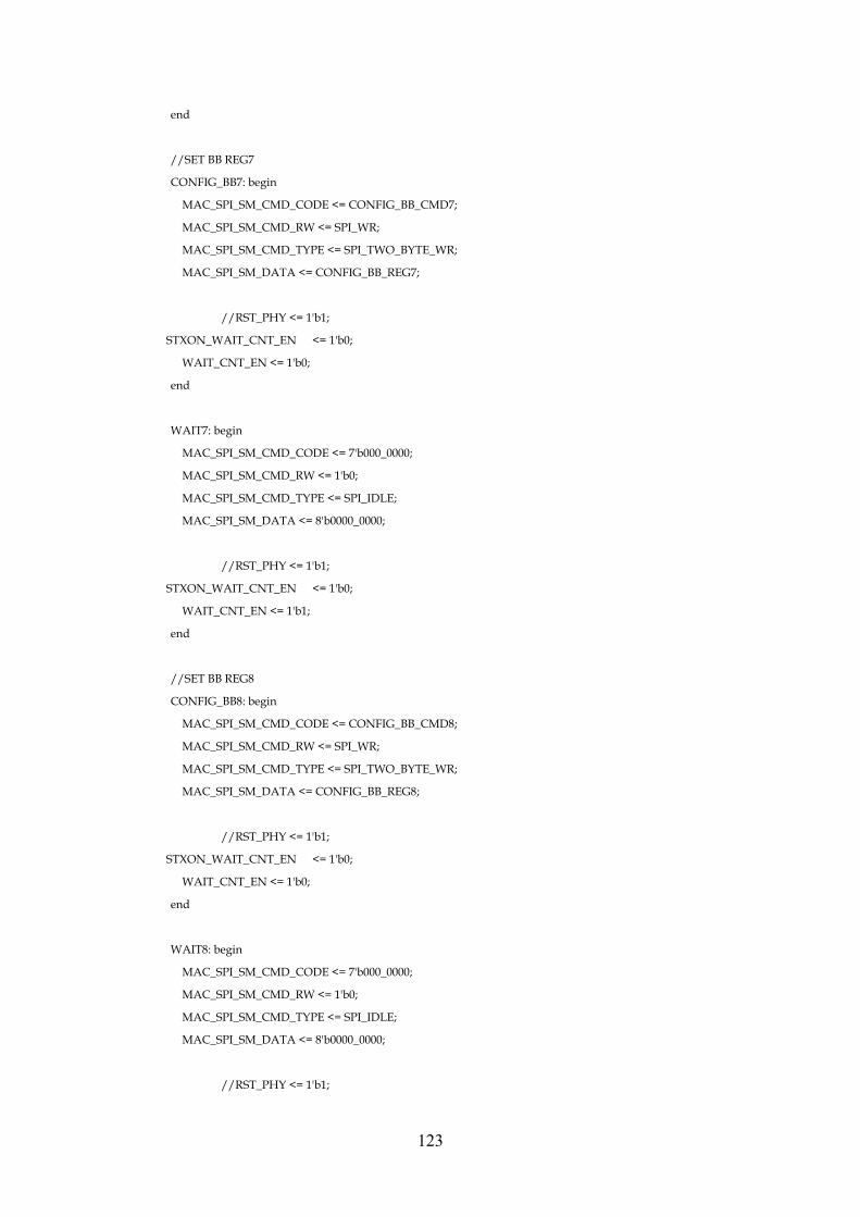
123
end
//SET BB REG7
CONFIG_BB7: begin
MAC_SPI_SM_CMD_CODE <= CONFIG_BB_CMD7;
MAC_SPI_SM_CMD_RW <= SPI_WR;
MAC_SPI_SM_CMD_TYPE <= SPI_TWO_BYTE_WR;
MAC_SPI_SM_DATA <= CONFIG_BB_REG7;
//RST_PHY <= 1'b1;
STXON_WAIT_CNT_EN <= 1'b0;
WAIT_CNT_EN <= 1'b0;
end
WAIT7: begin
MAC_SPI_SM_CMD_CODE <= 7'b000_0000;
MAC_SPI_SM_CMD_RW <= 1'b0;
MAC_SPI_SM_CMD_TYPE <= SPI_IDLE;
MAC_SPI_SM_DATA <= 8'b0000_0000;
//RST_PHY <= 1'b1;
STXON_WAIT_CNT_EN <= 1'b0;
WAIT_CNT_EN <= 1'b1;
end
//SET BB REG8
CONFIG_BB8: begin
MAC_SPI_SM_CMD_CODE <= CONFIG_BB_CMD8;
MAC_SPI_SM_CMD_RW <= SPI_WR;
MAC_SPI_SM_CMD_TYPE <= SPI_TWO_BYTE_WR;
MAC_SPI_SM_DATA <= CONFIG_BB_REG8;
//RST_PHY <= 1'b1;
STXON_WAIT_CNT_EN <= 1'b0;
WAIT_CNT_EN <= 1'b0;
end
WAIT8: begin
MAC_SPI_SM_CMD_CODE <= 7'b000_0000;
MAC_SPI_SM_CMD_RW <= 1'b0;
MAC_SPI_SM_CMD_TYPE <= SPI_IDLE;
MAC_SPI_SM_DATA <= 8'b0000_0000;
//RST_PHY <= 1'b1;
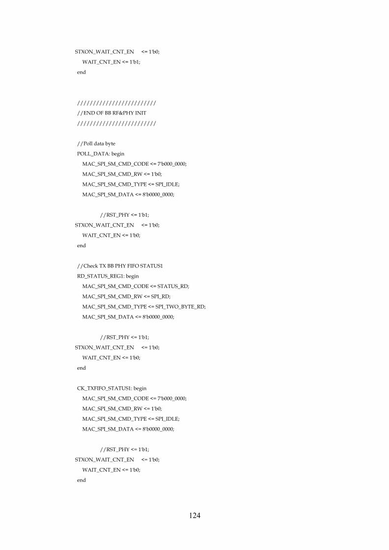
124
STXON_WAIT_CNT_EN <= 1'b0;
WAIT_CNT_EN <= 1'b1;
end
/////////////////////////
//END OF BB RF&PHY INIT
/////////////////////////
//Poll data byte
POLL_DATA: begin
MAC_SPI_SM_CMD_CODE <= 7'b000_0000;
MAC_SPI_SM_CMD_RW <= 1'b0;
MAC_SPI_SM_CMD_TYPE <= SPI_IDLE;
MAC_SPI_SM_DATA <= 8'b0000_0000;
//RST_PHY <= 1'b1;
STXON_WAIT_CNT_EN <= 1'b0;
WAIT_CNT_EN <= 1'b0;
end
//Check TX BB PHY FIFO STATUS1
RD_STATUS_REG1: begin
MAC_SPI_SM_CMD_CODE <= STATUS_RD;
MAC_SPI_SM_CMD_RW <= SPI_RD;
MAC_SPI_SM_CMD_TYPE <= SPI_TWO_BYTE_RD;
MAC_SPI_SM_DATA <= 8'b0000_0000;
//RST_PHY <= 1'b1;
STXON_WAIT_CNT_EN <= 1'b0;
WAIT_CNT_EN <= 1'b0;
end
CK_TXFIFO_STATUS1: begin
MAC_SPI_SM_CMD_CODE <= 7'b000_0000;
MAC_SPI_SM_CMD_RW <= 1'b0;
MAC_SPI_SM_CMD_TYPE <= SPI_IDLE;
MAC_SPI_SM_DATA <= 8'b0000_0000;
//RST_PHY <= 1'b1;
STXON_WAIT_CNT_EN <= 1'b0;
WAIT_CNT_EN <= 1'b0;
end
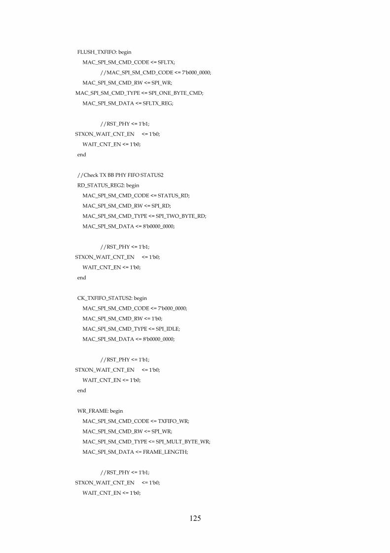
125
FLUSH_TXFIFO: begin
MAC_SPI_SM_CMD_CODE <= SFLTX;
//MAC_SPI_SM_CMD_CODE <= 7'b000_0000;
MAC_SPI_SM_CMD_RW <= SPI_WR;
MAC_SPI_SM_CMD_TYPE <= SPI_ONE_BYTE_CMD;
MAC_SPI_SM_DATA <= SFLTX_REG;
//RST_PHY <= 1'b1;
STXON_WAIT_CNT_EN <= 1'b0;
WAIT_CNT_EN <= 1'b0;
end
//Check TX BB PHY FIFO STATUS2
RD_STATUS_REG2: begin
MAC_SPI_SM_CMD_CODE <= STATUS_RD;
MAC_SPI_SM_CMD_RW <= SPI_RD;
MAC_SPI_SM_CMD_TYPE <= SPI_TWO_BYTE_RD;
MAC_SPI_SM_DATA <= 8'b0000_0000;
//RST_PHY <= 1'b1;
STXON_WAIT_CNT_EN <= 1'b0;
WAIT_CNT_EN <= 1'b0;
end
CK_TXFIFO_STATUS2: begin
MAC_SPI_SM_CMD_CODE <= 7'b000_0000;
MAC_SPI_SM_CMD_RW <= 1'b0;
MAC_SPI_SM_CMD_TYPE <= SPI_IDLE;
MAC_SPI_SM_DATA <= 8'b0000_0000;
//RST_PHY <= 1'b1;
STXON_WAIT_CNT_EN <= 1'b0;
WAIT_CNT_EN <= 1'b0;
end
WR_FRAME: begin
MAC_SPI_SM_CMD_CODE <= TXFIFO_WR;
MAC_SPI_SM_CMD_RW <= SPI_WR;
MAC_SPI_SM_CMD_TYPE <= SPI_MULT_BYTE_WR;
MAC_SPI_SM_DATA <= FRAME_LENGTH;
//RST_PHY <= 1'b1;
STXON_WAIT_CNT_EN <= 1'b0;
WAIT_CNT_EN <= 1'b0;
126
end
//Check TX BB PHY FIFO STATUS3
RD_STATUS_REG3: begin
MAC_SPI_SM_CMD_CODE <= STATUS_RD;
MAC_SPI_SM_CMD_RW <= SPI_RD;
MAC_SPI_SM_CMD_TYPE <= SPI_TWO_BYTE_RD;
MAC_SPI_SM_DATA <= 8'b0000_0000;
//RST_PHY <= 1'b1;
STXON_WAIT_CNT_EN <= 1'b0;
WAIT_CNT_EN <= 1'b0;
end
CK_TXFIFO_STATUS3: begin
MAC_SPI_SM_CMD_CODE <= 7'b000_0000;
MAC_SPI_SM_CMD_RW <= 1'b0;
MAC_SPI_SM_CMD_TYPE <= SPI_IDLE;
MAC_SPI_SM_DATA <= 8'b0000_0000;
//RST_PHY <= 1'b1;
STXON_WAIT_CNT_EN <= 1'b0;
WAIT_CNT_EN <= 1'b0;
end
//SET_STXON
SET_STXON: begin
MAC_SPI_SM_CMD_CODE <= STXON;
MAC_SPI_SM_CMD_RW <= SPI_WR;
MAC_SPI_SM_CMD_TYPE <= SPI_ONE_BYTE_CMD;
MAC_SPI_SM_DATA <= STXON_REG;
//RST_PHY <= 1'b1;
STXON_WAIT_CNT_EN <= 1'b0;
WAIT_CNT_EN <= 1'b0;
end
//Check TX BB PHY FIFO STATUS4
RD_STATUS_REG4: begin
MAC_SPI_SM_CMD_CODE <= STATUS_RD;
MAC_SPI_SM_CMD_RW <= SPI_RD;
MAC_SPI_SM_CMD_TYPE <= SPI_TWO_BYTE_RD;
MAC_SPI_SM_DATA <= 8'b0000_0000;
127
//RST_PHY <= 1'b1;
STXON_WAIT_CNT_EN <= 1'b0;
WAIT_CNT_EN <= 1'b0;
end
CK_TXFIFO_STATUS4: begin
MAC_SPI_SM_CMD_CODE <= 7'b000_0000;
MAC_SPI_SM_CMD_RW <= 1'b0;
MAC_SPI_SM_CMD_TYPE <= SPI_IDLE;
MAC_SPI_SM_DATA <= 8'b0000_0000;
//RST_PHY <= 1'b1;
STXON_WAIT_CNT_EN <= 1'b0;
WAIT_CNT_EN <= 1'b0;
end
CNTR_STXON: begin
MAC_SPI_SM_CMD_CODE <= 7'b000_0000;
MAC_SPI_SM_CMD_RW <= 1'b0;
MAC_SPI_SM_CMD_TYPE <= SPI_IDLE;
MAC_SPI_SM_DATA <= 8'b0000_0000;
//RST_PHY <= 1'b1;
STXON_WAIT_CNT_EN <= 1'b1;
WAIT_CNT_EN <= 1'b0;
end
default: begin
MAC_SPI_SM_CMD_CODE <= 7'b000_0000;
MAC_SPI_SM_CMD_RW <= 1'b0;
MAC_SPI_SM_CMD_TYPE <= SPI_IDLE;
MAC_SPI_SM_DATA <= 8'b0000_0000;
//RST_PHY <= 1'b1;
STXON_WAIT_CNT_EN <= 1'b0;
WAIT_CNT_EN <= 1'b0;
end
endcase
end //output assignment
///////////////////////////
// CONGFIGURE WAIT COUNTER
///////////////////////////
128
always @(posedge MAC_SPI_SM_CLK or negedge MAC_SPI_SM_RSTN)
begin
if (~MAC_SPI_SM_RSTN)
CONFIG_WAIT_CNT <= 0;
else if (CONFIG_WAIT_CNT == WAIT_CYCLES)
CONFIG_WAIT_CNT <= 0;
else if (WAIT_CNT_EN == 1'b1)
CONFIG_WAIT_CNT <= CONFIG_WAIT_CNT + 1;
end
always @(posedge MAC_SPI_SM_CLK or negedge MAC_SPI_SM_RSTN)
begin
if (~MAC_SPI_SM_RSTN)
STXON_WAIT_CNT <= 11'b0;
else
begin
if (MAC_SPI_SM_EN_TX)
begin
if (STXON_WAIT_CNT == STXON_WAIT_CYCLES)
STXON_WAIT_CNT <= 11'b0;
else
begin
if (STXON_WAIT_CNT_EN == 1'b1)
STXON_WAIT_CNT <= STXON_WAIT_CNT + 1;
else
STXON_WAIT_CNT <= 11'b0;
end
end
else
STXON_WAIT_CNT <= 11'b0;
end
end
endmodule //BPRO_TX_BB_MAC_SPI_SM
129
Appendix E: Verilog RTL code of SPI decoder for transmitter
////////////////
// TOP MODULE //
////////////////
module BPRO_TX_BB_MAC_SPI_DECODER (
//input
MAC_SPI_DECODER_RSTN,
MAC_SPI_DECODER_SCLK,
MAC_SPI_DECODER_CSN,
MAC_SPI_DECODER_CTRL_SI,
MAC_SPI_DECODER_BB_SI,
//output
MAC_SPI_DECODER_REG,
MAC_SPI_DECODER_VALID_REG
);
////////////
// INPUTS //
////////////
input MAC_SPI_DECODER_RSTN;
input MAC_SPI_DECODER_SCLK;
input MAC_SPI_DECODER_CSN;
input MAC_SPI_DECODER_CTRL_SI;
input MAC_SPI_DECODER_BB_SI;
/////////////
// OUTPUTS //
/////////////
output [7:0] MAC_SPI_DECODER_REG;
output MAC_SPI_DECODER_VALID_REG;
/////////////////////////
// SIGNAL DECLARATIONS //
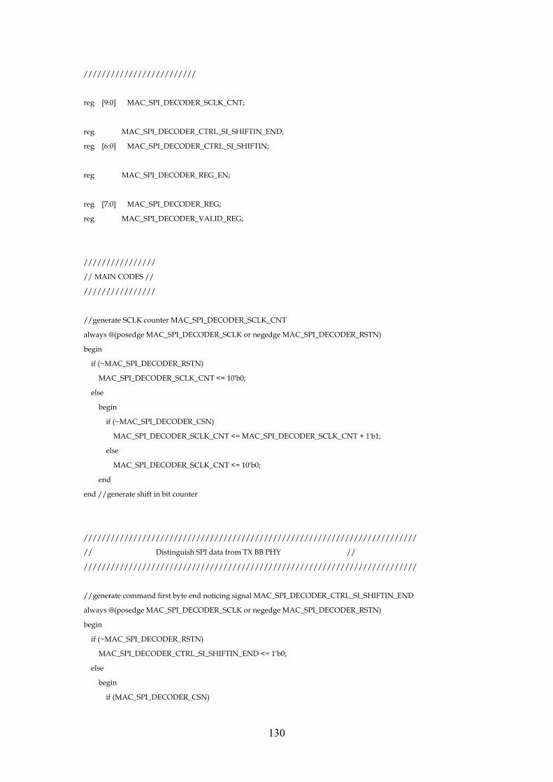
130
/////////////////////////
reg [9:0] MAC_SPI_DECODER_SCLK_CNT;
reg MAC_SPI_DECODER_CTRL_SI_SHIFTIN_END;
reg [6:0] MAC_SPI_DECODER_CTRL_SI_SHIFTIN;
reg MAC_SPI_DECODER_REG_EN;
reg [7:0] MAC_SPI_DECODER_REG;
reg MAC_SPI_DECODER_VALID_REG;
////////////////
// MAIN CODES //
////////////////
//generate SCLK counter MAC_SPI_DECODER_SCLK_CNT
always @(posedge MAC_SPI_DECODER_SCLK or negedge MAC_SPI_DECODER_RSTN)
begin
if (~MAC_SPI_DECODER_RSTN)
MAC_SPI_DECODER_SCLK_CNT <= 10'b0;
else
begin
if (~MAC_SPI_DECODER_CSN)
MAC_SPI_DECODER_SCLK_CNT <= MAC_SPI_DECODER_SCLK_CNT + 1'b1;
else
MAC_SPI_DECODER_SCLK_CNT <= 10'b0;
end
end //generate shift in bit counter
//////////////////////////////////////////////////////////////////////////
// Distinguish SPI data from TX BB PHY //
//////////////////////////////////////////////////////////////////////////
//generate command first byte end noticing signal MAC_SPI_DECODER_CTRL_SI_SHIFTIN_END
always @(posedge MAC_SPI_DECODER_SCLK or negedge MAC_SPI_DECODER_RSTN)
begin
if (~MAC_SPI_DECODER_RSTN)
MAC_SPI_DECODER_CTRL_SI_SHIFTIN_END <= 1'b0;
else
begin
if (MAC_SPI_DECODER_CSN)
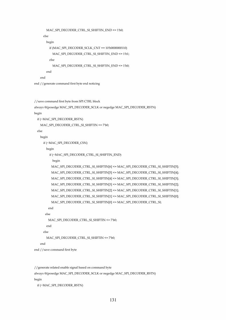
131
MAC_SPI_DECODER_CTRL_SI_SHIFTIN_END <= 1'b0;
else
begin
if (MAC_SPI_DECODER_SCLK_CNT == 10'b0000000110)
MAC_SPI_DECODER_CTRL_SI_SHIFTIN_END <= 1'b1;
else
MAC_SPI_DECODER_CTRL_SI_SHIFTIN_END <= 1'b0;
end
end
end //generate command first byte end noticing
//save command first byte from SPI CTRL block
always @(posedge MAC_SPI_DECODER_SCLK or negedge MAC_SPI_DECODER_RSTN)
begin
if (~MAC_SPI_DECODER_RSTN)
MAC_SPI_DECODER_CTRL_SI_SHIFTIN <= 7'b0;
else
begin
if (~MAC_SPI_DECODER_CSN)
begin
if (~MAC_SPI_DECODER_CTRL_SI_SHIFTIN_END)
begin
MAC_SPI_DECODER_CTRL_SI_SHIFTIN[6] <= MAC_SPI_DECODER_CTRL_SI_SHIFTIN[5];
MAC_SPI_DECODER_CTRL_SI_SHIFTIN[5] <= MAC_SPI_DECODER_CTRL_SI_SHIFTIN[4];
MAC_SPI_DECODER_CTRL_SI_SHIFTIN[4] <= MAC_SPI_DECODER_CTRL_SI_SHIFTIN[3];
MAC_SPI_DECODER_CTRL_SI_SHIFTIN[3] <= MAC_SPI_DECODER_CTRL_SI_SHIFTIN[2];
MAC_SPI_DECODER_CTRL_SI_SHIFTIN[2] <= MAC_SPI_DECODER_CTRL_SI_SHIFTIN[1];
MAC_SPI_DECODER_CTRL_SI_SHIFTIN[1] <= MAC_SPI_DECODER_CTRL_SI_SHIFTIN[0];
MAC_SPI_DECODER_CTRL_SI_SHIFTIN[0] <= MAC_SPI_DECODER_CTRL_SI;
end
else
MAC_SPI_DECODER_CTRL_SI_SHIFTIN <= 7'b0;
end
else
MAC_SPI_DECODER_CTRL_SI_SHIFTIN <= 7'b0;
end
end //save command first byte
//generate related enable signal based on command byte
always @(posedge MAC_SPI_DECODER_SCLK or negedge MAC_SPI_DECODER_RSTN)
begin
if (~MAC_SPI_DECODER_RSTN)

132
begin
MAC_SPI_DECODER_REG_EN <= 1'b0;
end
else
begin
if (~MAC_SPI_DECODER_CSN)
begin
if (MAC_SPI_DECODER_CTRL_SI_SHIFTIN_END)
begin
case ({MAC_SPI_DECODER_CTRL_SI_SHIFTIN[6:0], MAC_SPI_DECODER_CTRL_SI})
8'b00001010,
8'b00001100,
8'b00001110,
8'b00010100,
8'b00010110,
8'b00011000,
8'b00011010,
8'b00011100,
8'b00011110,
8'b00100000,
8'b00100010,
8'b00100100,
8'b00100110,
8'b00101000,
8'b00101100,
8'b00101110,
8'b00110000,
8'b01000000,
8'b01000010,
8'b01000100,
8'b01000110,
8'b01001000,
8'b01001010,
8'b01001100,
8'b01001110,
8'b01010000,
8'b01010010,
8'b01010100,
8'b01100000,
8'b01100010:
begin
MAC_SPI_DECODER_REG_EN <= 1'b1;
end
default:
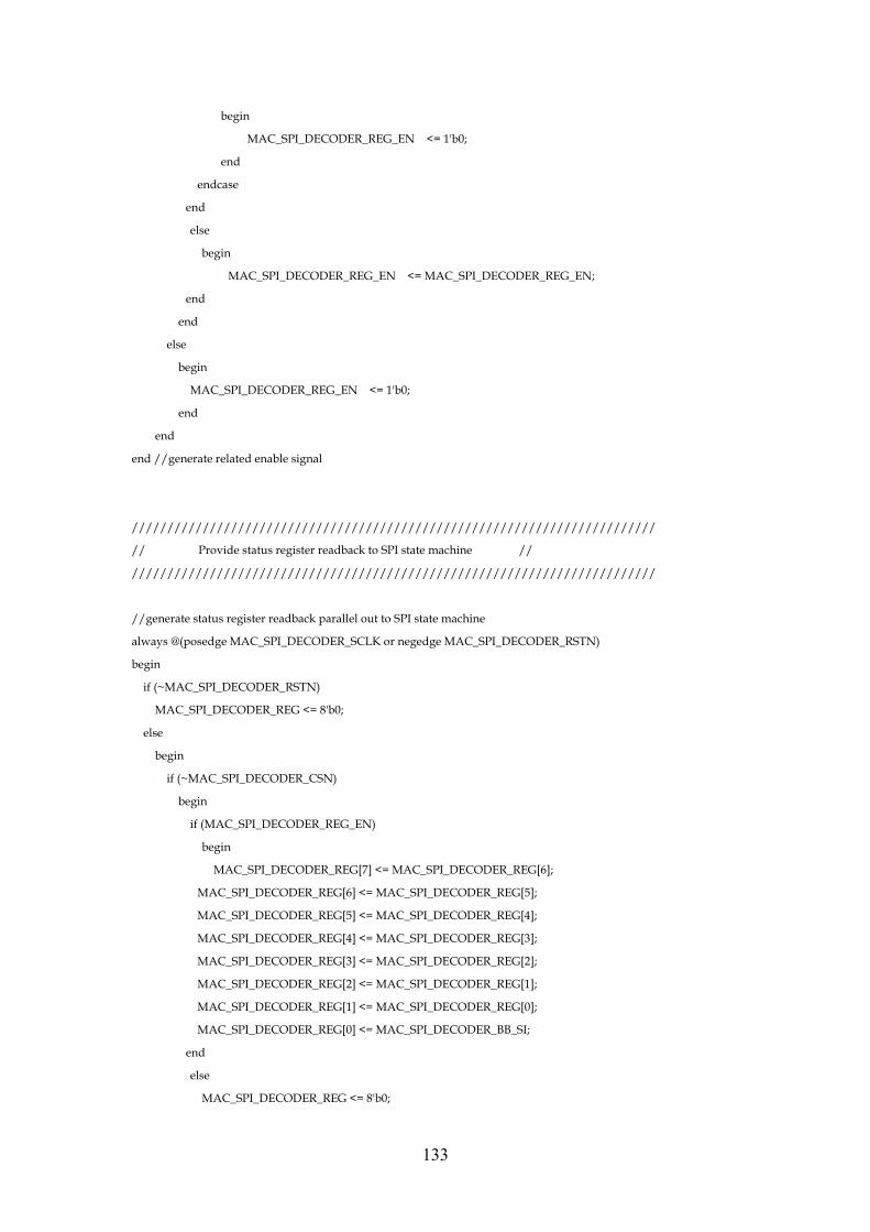
133
begin
MAC_SPI_DECODER_REG_EN <= 1'b0;
end
endcase
end
else
begin
MAC_SPI_DECODER_REG_EN <= MAC_SPI_DECODER_REG_EN;
end
end
else
begin
MAC_SPI_DECODER_REG_EN <= 1'b0;
end
end
end //generate related enable signal
//////////////////////////////////////////////////////////////////////////
// Provide status register readback to SPI state machine //
//////////////////////////////////////////////////////////////////////////
//generate status register readback parallel out to SPI state machine
always @(posedge MAC_SPI_DECODER_SCLK or negedge MAC_SPI_DECODER_RSTN)
begin
if (~MAC_SPI_DECODER_RSTN)
MAC_SPI_DECODER_REG <= 8'b0;
else
begin
if (~MAC_SPI_DECODER_CSN)
begin
if (MAC_SPI_DECODER_REG_EN)
begin
MAC_SPI_DECODER_REG[7] <= MAC_SPI_DECODER_REG[6];
MAC_SPI_DECODER_REG[6] <= MAC_SPI_DECODER_REG[5];
MAC_SPI_DECODER_REG[5] <= MAC_SPI_DECODER_REG[4];
MAC_SPI_DECODER_REG[4] <= MAC_SPI_DECODER_REG[3];
MAC_SPI_DECODER_REG[3] <= MAC_SPI_DECODER_REG[2];
MAC_SPI_DECODER_REG[2] <= MAC_SPI_DECODER_REG[1];
MAC_SPI_DECODER_REG[1] <= MAC_SPI_DECODER_REG[0];
MAC_SPI_DECODER_REG[0] <= MAC_SPI_DECODER_BB_SI;
end
else
MAC_SPI_DECODER_REG <= 8'b0;

134
end
else
MAC_SPI_DECODER_REG <= 8'b0;
end
end //generate status register readback
//generate status register readback parallel out valid signal MAC_SPI_DECODER_VALID_REG
always @(posedge MAC_SPI_DECODER_SCLK or negedge MAC_SPI_DECODER_RSTN)
begin
if (~MAC_SPI_DECODER_RSTN)
MAC_SPI_DECODER_VALID_REG <= 1'b0;
else
begin
if (MAC_SPI_DECODER_REG_EN)
begin
if (MAC_SPI_DECODER_SCLK_CNT == 10'b0000001110)
MAC_SPI_DECODER_VALID_REG <= 1'b1;
else
MAC_SPI_DECODER_VALID_REG <= 1'b0;
end
else
MAC_SPI_DECODER_VALID_REG <= 1'b0;
end
end //generate status register readback parallel out valid
endmodule //BPRO_TX_BB_MAC_SPI_DECODER

135
Appendix F: Verilog RTL code of microcontroller for receiver
////////////////
// TOP MODULE
////////////////
module BPRO_RX_BB_MAC_SPI_SM(
//input
MAC_SPI_SM_CLK,
MAC_SPI_SM_RSTN,
MAC_SPI_SM_EOS,
MAC_SPI_SM_PHY_IRQ,
MAC_SPI_SM_PHY_REG,
MAC_SPI_SM_VALID_PHY_REG,
//output
MAC_SPI_SM_SOS,
MAC_RX_BUSY,
//RST_PHY,
MAC_SPI_SM_CMD_CODE,
MAC_SPI_SM_CMD_RW,
MAC_SPI_SM_CMD_TYPE,
MAC_SPI_SM_DATA
);
///////////////
// PARAMETERS
///////////////
//SPI command codes
parameter [6:0] PLL_CTRL_RX = 7'b010_0100,
PA_CTRL_RX = 7'b001_0000,
FRACN_HI_RX = 7'b010_0101,
BB_CTRL = 7'b000_0111,
PS_CTRL_RX = 7'b010_0010,
FRACN_MI_RX = 7'b010_0110,
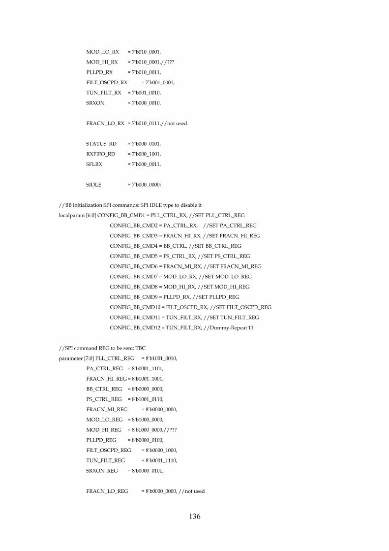
136
MOD_LO_RX = 7'b010_0001,
MOD_HI_RX = 7'b010_0001,//???
PLLPD_RX = 7'b010_0011,
FILT_OSCPD_RX = 7'b001_0001,
TUN_FILT_RX = 7'b001_0010,
SRXON = 7'b000_0010,
FRACN_LO_RX = 7'b010_0111,//not used
STATUS_RD = 7'b000_0101,
RXFIFO_RD = 7'b000_1001,
SFLRX = 7'b000_0011,
SIDLE = 7'b000_0000;
//BB initialization SPI commands: SPI IDLE type to disable it
localparam [6:0] CONFIG_BB_CMD1 = PLL_CTRL_RX, //SET PLL_CTRL_REG
CONFIG_BB_CMD2 = PA_CTRL_RX, //SET PA_CTRL_REG
CONFIG_BB_CMD3 = FRACN_HI_RX, //SET FRACN_HI_REG
CONFIG_BB_CMD4 = BB_CTRL, //SET BB_CTRL_REG
CONFIG_BB_CMD5 = PS_CTRL_RX, //SET PS_CTRL_REG
CONFIG_BB_CMD6 = FRACN_MI_RX, //SET FRACN_MI_REG
CONFIG_BB_CMD7 = MOD_LO_RX, //SET MOD_LO_REG
CONFIG_BB_CMD8 = MOD_HI_RX, //SET MOD_HI_REG
CONFIG_BB_CMD9 = PLLPD_RX, //SET PLLPD_REG
CONFIG_BB_CMD10 = FILT_OSCPD_RX, //SET FILT_OSCPD_REG
CONFIG_BB_CMD11 = TUN_FILT_RX, //SET TUN_FILT_REG
CONFIG_BB_CMD12 = TUN_FILT_RX; //Dummy-Repeat 11
//SPI command REG to be sent: TBC
parameter [7:0] PLL_CTRL_REG = 8'b1001_0010,
PA_CTRL_REG = 8'b0001_1101,
FRACN_HI_REG = 8'b1001_1001,
BB_CTRL_REG = 8'b0000_0000,
PS_CTRL_REG = 8'b1001_0110,
FRACN_MI_REG = 8'b0000_0000,
MOD_LO_REG = 8'b1000_0000,
MOD_HI_REG = 8'b1000_0000,//???
PLLPD_REG = 8'b0000_0100,
FILT_OSCPD_REG = 8'b0000_1000,
TUN_FILT_REG = 8'b0001_1110,
SRXON_REG = 8'b0000_0101,
FRACN_LO_REG = 8'b0000_0000, //not used

137
SFLRX_REG = 8'b0000_0000,
SIDLE_REG = 8'b0000_0000;
//BB initialization SPI registers
localparam [7:0] CONFIG_BB_REG1 = PLL_CTRL_REG, //SET PLL_CTRL_REG
CONFIG_BB_REG2 = PA_CTRL_REG, //SET PA_CTRL_REG
CONFIG_BB_REG3 = FRACN_HI_REG, //SET FRACN_HI_REG
CONFIG_BB_REG4 = BB_CTRL_REG, //SET BB_CTRL_REG CRC OFF
CONFIG_BB_REG5 = PS_CTRL_REG, //SET PS_CTRL_REG
CONFIG_BB_REG6 = FRACN_MI_REG, //SET FRACN_MI_REG
CONFIG_BB_REG7 = MOD_LO_REG, //SET MOD_LO_REG
CONFIG_BB_REG8 = MOD_HI_REG, //SET MOD_HI_REG
CONFIG_BB_REG9 = PLLPD_REG, //SET PLLPD_REG
CONFIG_BB_REG10 = FILT_OSCPD_REG, //SET FILT_OSCPD_REG
CONFIG_BB_REG11 = TUN_FILT_REG, //SET TUN_FILT_REG
CONFIG_BB_REG12 = TUN_FILT_REG; //Dummy-Repeat 11
//SPI data length: number of bytes
parameter SPI_DATA_OUT_MAX_BYTE = 1;
//SPI command RW
parameter SPI_RD = 0,
SPI_WR = 1;
//WAIT counter width
parameter WAIT_CNT_W = 4;
//WAIT length
parameter [3:0] WAIT_CYCLES = 4'b1111;
//SPI command types
parameter [2:0] SPI_IDLE = 0, //DO NOTHING
SPI_ONE_BYTE_CMD = 1, //ALWAYS WR
SPI_TWO_BYTE_WR = 2,
SPI_TWO_BYTE_RD = 3,
SPI_MULT_BYTE_RD = 4,
SPI_MULT_BYTE_WR = 5; //NOT USED IN THIS DESIGN
//state machine states
parameter [5:0] RST_STATE = 0,
CONFIG_BB1 = 1, //SET PLL_CTRL_REG
WAIT1 = 2,

138
CONFIG_BB2 = 3, //SET PA_CTRL_REG
WAIT2 = 4,
CONFIG_BB3 = 5, //SET FRACN_HI_REG
WAIT3 = 6,
CONFIG_BB4 = 7, //SET BB_CTRL_REG CRC OFF
WAIT4 = 8,
CONFIG_BB5 = 9, //SET PS_CTRL_REG
WAIT5 = 10,
CONFIG_BB6 = 11, //SET FRACN_MI_REG
WAIT6 = 12,
CONFIG_BB7 = 13, //SET MOD_LO_REG
WAIT7 = 14,
CONFIG_BB8 = 15, //SET MOD_HI_REG
WAIT8 = 16,
CONFIG_BB9 = 17, //SET PLLPD_REG
WAIT9 = 18,
CONFIG_BB10 = 19, //SET FILT_OSCPD_REG
WAIT10 = 20,
CONFIG_BB11 = 21, //SET TUN_FILT_REG
WAIT11 = 22,
CONFIG_BB12 = 23, //Dummy-Repeat 11
WAIT12 = 24,
POLL_IRQ = 25,
RD_STATUS_REG1 = 26,
CK_RXFIFO_STATUS1 = 27,
RD_FRAME = 28,
RD_STATUS_REG2 = 29,
CK_RXFIFO_STATUS2 = 30,
FLUSH_RXFIFO = 31,
RD_STATUS_REG3 = 32,
CK_RXFIFO_STATUS3 = 33,
SET_SRXON = 34,
SET_SIDLE1 = 35,
SET_SIDLE2 = 36;
///////////
// INPUTS
///////////
input MAC_SPI_SM_CLK;
input MAC_SPI_SM_RSTN;
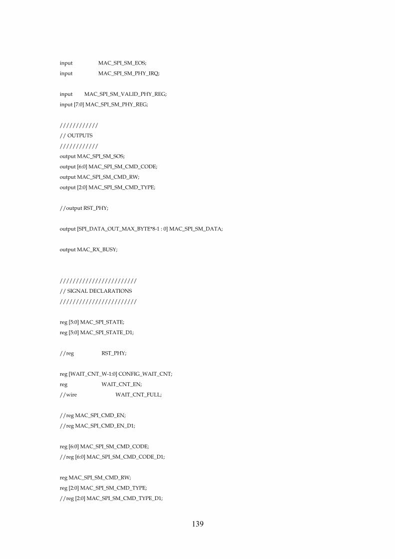
139
input MAC_SPI_SM_EOS;
input MAC_SPI_SM_PHY_IRQ;
input MAC_SPI_SM_VALID_PHY_REG;
input [7:0] MAC_SPI_SM_PHY_REG;
////////////
// OUTPUTS
////////////
output MAC_SPI_SM_SOS;
output [6:0] MAC_SPI_SM_CMD_CODE;
output MAC_SPI_SM_CMD_RW;
output [2:0] MAC_SPI_SM_CMD_TYPE;
//output RST_PHY;
output [SPI_DATA_OUT_MAX_BYTE*8-1 : 0] MAC_SPI_SM_DATA;
output MAC_RX_BUSY;
////////////////////////
// SIGNAL DECLARATIONS
////////////////////////
reg [5:0] MAC_SPI_STATE;
reg [5:0] MAC_SPI_STATE_D1;
//reg RST_PHY;
reg [WAIT_CNT_W-1:0] CONFIG_WAIT_CNT;
reg WAIT_CNT_EN;
//wire WAIT_CNT_FULL;
//reg MAC_SPI_CMD_EN;
//reg MAC_SPI_CMD_EN_D1;
reg [6:0] MAC_SPI_SM_CMD_CODE;
//reg [6:0] MAC_SPI_SM_CMD_CODE_D1;
reg MAC_SPI_SM_CMD_RW;
reg [2:0] MAC_SPI_SM_CMD_TYPE;
//reg [2:0] MAC_SPI_SM_CMD_TYPE_D1;
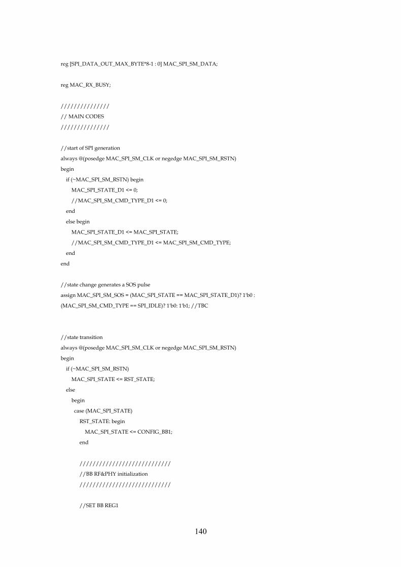
140
reg [SPI_DATA_OUT_MAX_BYTE*8-1 : 0] MAC_SPI_SM_DATA;
reg MAC_RX_BUSY;
///////////////
// MAIN CODES
///////////////
//start of SPI generation
always @(posedge MAC_SPI_SM_CLK or negedge MAC_SPI_SM_RSTN)
begin
if (~MAC_SPI_SM_RSTN) begin
MAC_SPI_STATE_D1 <= 0;
//MAC_SPI_SM_CMD_TYPE_D1 <= 0;
end
else begin
MAC_SPI_STATE_D1 <= MAC_SPI_STATE;
//MAC_SPI_SM_CMD_TYPE_D1 <= MAC_SPI_SM_CMD_TYPE;
end
end
//state change generates a SOS pulse
assign MAC_SPI_SM_SOS = (MAC_SPI_STATE == MAC_SPI_STATE_D1)? 1'b0 :
(MAC_SPI_SM_CMD_TYPE == SPI_IDLE)? 1'b0: 1'b1; //TBC
//state transition
always @(posedge MAC_SPI_SM_CLK or negedge MAC_SPI_SM_RSTN)
begin
if (~MAC_SPI_SM_RSTN)
MAC_SPI_STATE <= RST_STATE;
else
begin
case (MAC_SPI_STATE)
RST_STATE: begin
MAC_SPI_STATE <= CONFIG_BB1;
end
////////////////////////////
//BB RF&PHY initialization
////////////////////////////
//SET BB REG1

141
CONFIG_BB1: begin
if (MAC_SPI_SM_EOS == 1'b1)
MAC_SPI_STATE <= WAIT1;
else
MAC_SPI_STATE <= CONFIG_BB1;
end
WAIT1: begin
if (CONFIG_WAIT_CNT == WAIT_CYCLES)
MAC_SPI_STATE <= CONFIG_BB2;
else
MAC_SPI_STATE <= WAIT1;
end
//SET BB REG2
CONFIG_BB2: begin
if (MAC_SPI_SM_EOS == 1'b1)
MAC_SPI_STATE <= WAIT2;
else
MAC_SPI_STATE <= CONFIG_BB2;
end
WAIT2: begin
if (CONFIG_WAIT_CNT == WAIT_CYCLES)
MAC_SPI_STATE <= CONFIG_BB3;
else
MAC_SPI_STATE <= WAIT2;
end
//SET BB REG3
CONFIG_BB3: begin
if (MAC_SPI_SM_EOS == 1'b1)
MAC_SPI_STATE <= WAIT3;
else
MAC_SPI_STATE <= CONFIG_BB3;
end
WAIT3: begin
if (CONFIG_WAIT_CNT == WAIT_CYCLES)
MAC_SPI_STATE <= CONFIG_BB4;
else
MAC_SPI_STATE <= WAIT3;
end

142
//SET BB REG4
CONFIG_BB4: begin
if (MAC_SPI_SM_EOS == 1'b1)
MAC_SPI_STATE <= WAIT4;
else
MAC_SPI_STATE <= CONFIG_BB4;
end
WAIT4: begin
if (CONFIG_WAIT_CNT == WAIT_CYCLES)
MAC_SPI_STATE <= CONFIG_BB5;
else
MAC_SPI_STATE <= WAIT4;
end
//SET BB REG5
CONFIG_BB5: begin
if (MAC_SPI_SM_EOS == 1'b1)
MAC_SPI_STATE <= WAIT5;
else
MAC_SPI_STATE <= CONFIG_BB5;
end
WAIT5: begin
if (CONFIG_WAIT_CNT == WAIT_CYCLES)
MAC_SPI_STATE <= CONFIG_BB6;
else
MAC_SPI_STATE <= WAIT5;
end
//SET BB REG6
CONFIG_BB6: begin
if (MAC_SPI_SM_EOS == 1'b1)
MAC_SPI_STATE <= WAIT6;
else
MAC_SPI_STATE <= CONFIG_BB6;
end
WAIT6: begin
if (CONFIG_WAIT_CNT == WAIT_CYCLES)
MAC_SPI_STATE <= CONFIG_BB7;
else
MAC_SPI_STATE <= WAIT6;
end

143
//SET BB REG7
CONFIG_BB7: begin
if (MAC_SPI_SM_EOS == 1'b1)
MAC_SPI_STATE <= WAIT7;
else
MAC_SPI_STATE <= CONFIG_BB7;
end
WAIT7: begin
if (CONFIG_WAIT_CNT == WAIT_CYCLES)
MAC_SPI_STATE <= CONFIG_BB8;
else
MAC_SPI_STATE <= WAIT7;
end
//SET BB REG8
CONFIG_BB8: begin
if (MAC_SPI_SM_EOS == 1'b1)
MAC_SPI_STATE <= WAIT8;
else
MAC_SPI_STATE <= CONFIG_BB8;
end
WAIT8: begin
if (CONFIG_WAIT_CNT == WAIT_CYCLES)
MAC_SPI_STATE <= CONFIG_BB9;
else
MAC_SPI_STATE <= WAIT8;
end
//SET BB REG9
CONFIG_BB9: begin
if (MAC_SPI_SM_EOS == 1'b1)
MAC_SPI_STATE <= WAIT9;
else
MAC_SPI_STATE <= CONFIG_BB9;
end
WAIT9: begin
if (CONFIG_WAIT_CNT == WAIT_CYCLES)
MAC_SPI_STATE <= CONFIG_BB10;
else
MAC_SPI_STATE <= WAIT9;

144
end
//SET BB REG10
CONFIG_BB10: begin
if (MAC_SPI_SM_EOS == 1'b1)
MAC_SPI_STATE <= WAIT10;
else
MAC_SPI_STATE <= CONFIG_BB10;
end
WAIT10: begin
if (CONFIG_WAIT_CNT == WAIT_CYCLES)
MAC_SPI_STATE <= CONFIG_BB11;
else
MAC_SPI_STATE <= WAIT10;
end
//SET BB REG11
CONFIG_BB11: begin
if (MAC_SPI_SM_EOS == 1'b1)
MAC_SPI_STATE <= WAIT11;
else
MAC_SPI_STATE <= CONFIG_BB11;
end
WAIT11: begin
if (CONFIG_WAIT_CNT == WAIT_CYCLES)
MAC_SPI_STATE <= CONFIG_BB12;
else
MAC_SPI_STATE <= WAIT11;
end
//SET BB REG12
CONFIG_BB12: begin
if (MAC_SPI_SM_EOS == 1'b1)
MAC_SPI_STATE <= WAIT12;
else
MAC_SPI_STATE <= CONFIG_BB12;
end
WAIT12: begin
if (CONFIG_WAIT_CNT == WAIT_CYCLES)
MAC_SPI_STATE <= SET_SRXON;
else

145
MAC_SPI_STATE <= WAIT12;
end
///////////////////
// END OF BB INIT
///////////////////
SET_SRXON: begin
if (MAC_SPI_SM_EOS == 1'b1)
//MAC_SPI_STATE <= POLL_IRQ;
MAC_SPI_STATE <= RD_STATUS_REG1;
else
MAC_SPI_STATE <= SET_SRXON;
end
//Poll interruption bit
POLL_IRQ: begin
if (MAC_SPI_SM_PHY_IRQ == 1'b1)
MAC_SPI_STATE <= RD_STATUS_REG1;
else
MAC_SPI_STATE <= POLL_IRQ;
end
//RD_STATUS_REG1
RD_STATUS_REG1: begin
if (MAC_SPI_SM_VALID_PHY_REG == 1'b1)
MAC_SPI_STATE <= CK_RXFIFO_STATUS1;
else
MAC_SPI_STATE <= RD_STATUS_REG1;
end
//CK_RXFIFO_STATUS1
CK_RXFIFO_STATUS1: begin
//if (MAC_SPI_SM_FRAME_RDY == 1'b1)
//if (MAC_SPI_SM_VALID_PHY_REG == 1'b0)
// MAC_SPI_STATE <= CK_RXFIFO_STATUS1;
//else if (MAC_SPI_SM_PHY_REG[6] == 1'b1)
if (MAC_SPI_SM_PHY_REG[6] == 1'b1)
//MAC_SPI_STATE <= RD_FRAME;
MAC_SPI_STATE <= SET_SIDLE1;
else
//MAC_SPI_STATE <= POLL_IRQ;
MAC_SPI_STATE <= SET_SRXON;
end
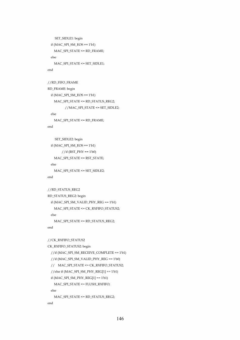
146
SET_SIDLE1: begin
if (MAC_SPI_SM_EOS == 1'b1)
MAC_SPI_STATE <= RD_FRAME;
else
MAC_SPI_STATE <= SET_SIDLE1;
end
//RD_FIFO_FRAME
RD_FRAME: begin
if (MAC_SPI_SM_EOS == 1'b1)
MAC_SPI_STATE <= RD_STATUS_REG2;
//MAC_SPI_STATE <= SET_SIDLE2;
else
MAC_SPI_STATE <= RD_FRAME;
end
SET_SIDLE2: begin
if (MAC_SPI_SM_EOS == 1'b1)
//if (RST_PHY == 1'b0)
MAC_SPI_STATE <= RST_STATE;
else
MAC_SPI_STATE <= SET_SIDLE2;
end
//RD_STATUS_REG2
RD_STATUS_REG2: begin
if (MAC_SPI_SM_VALID_PHY_REG == 1'b1)
MAC_SPI_STATE <= CK_RXFIFO_STATUS2;
else
MAC_SPI_STATE <= RD_STATUS_REG2;
end
//CK_RXFIFO_STATUS2
CK_RXFIFO_STATUS2: begin
//if (MAC_SPI_SM_RECEIVE_COMPLETE == 1'b1)
//if (MAC_SPI_SM_VALID_PHY_REG == 1'b0)
// MAC_SPI_STATE <= CK_RXFIFO_STATUS2;
//else if (MAC_SPI_SM_PHY_REG[1] == 1'b1)
if (MAC_SPI_SM_PHY_REG[1] == 1'b1)
MAC_SPI_STATE <= FLUSH_RXFIFO;
else
MAC_SPI_STATE <= RD_STATUS_REG2;
end
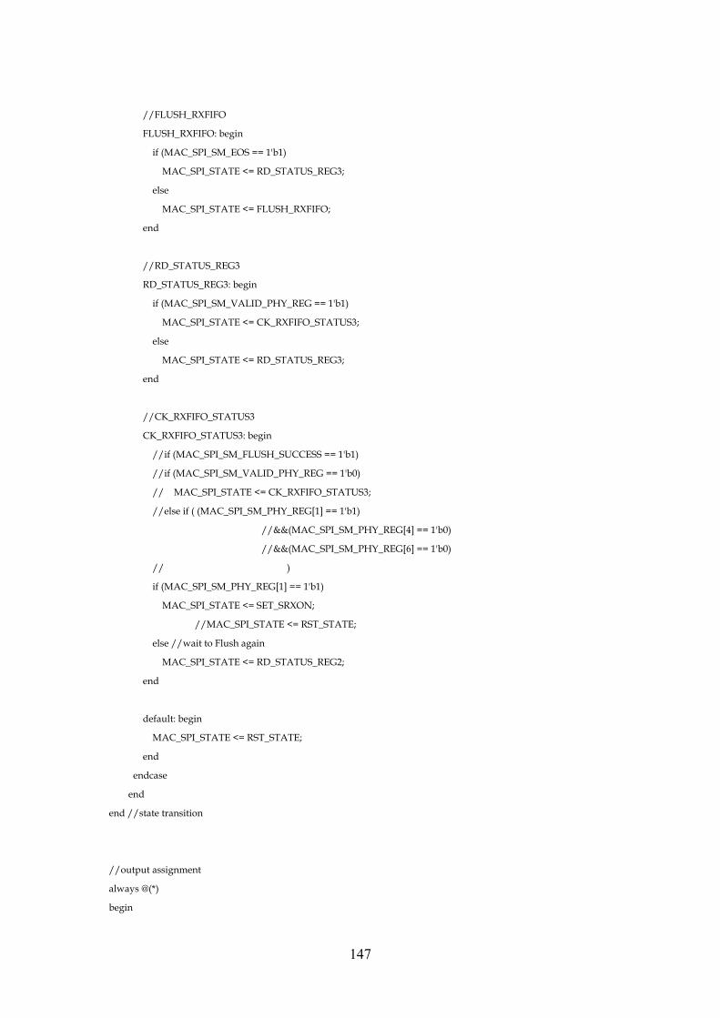
147
//FLUSH_RXFIFO
FLUSH_RXFIFO: begin
if (MAC_SPI_SM_EOS == 1'b1)
MAC_SPI_STATE <= RD_STATUS_REG3;
else
MAC_SPI_STATE <= FLUSH_RXFIFO;
end
//RD_STATUS_REG3
RD_STATUS_REG3: begin
if (MAC_SPI_SM_VALID_PHY_REG == 1'b1)
MAC_SPI_STATE <= CK_RXFIFO_STATUS3;
else
MAC_SPI_STATE <= RD_STATUS_REG3;
end
//CK_RXFIFO_STATUS3
CK_RXFIFO_STATUS3: begin
//if (MAC_SPI_SM_FLUSH_SUCCESS == 1'b1)
//if (MAC_SPI_SM_VALID_PHY_REG == 1'b0)
// MAC_SPI_STATE <= CK_RXFIFO_STATUS3;
//else if ( (MAC_SPI_SM_PHY_REG[1] == 1'b1)
//&&(MAC_SPI_SM_PHY_REG[4] == 1'b0)
//&&(MAC_SPI_SM_PHY_REG[6] == 1'b0)
// )
if (MAC_SPI_SM_PHY_REG[1] == 1'b1)
MAC_SPI_STATE <= SET_SRXON;
//MAC_SPI_STATE <= RST_STATE;
else //wait to Flush again
MAC_SPI_STATE <= RD_STATUS_REG2;
end
default: begin
MAC_SPI_STATE <= RST_STATE;
end
endcase
end
end //state transition
//output assignment
always @(*)
begin

148
case (MAC_SPI_STATE)
RST_STATE: begin
MAC_SPI_SM_CMD_CODE <= 7'b000_0000;
MAC_SPI_SM_CMD_RW <= 1'b0;
MAC_SPI_SM_CMD_TYPE <= 3'b000;
MAC_SPI_SM_DATA <= 8'b0000_0000;
//RST_PHY <= 1'b1;
WAIT_CNT_EN <= 1'b0;
end
///////////////////////////
//BB RF&PHY initialization
///////////////////////////
//SET BB REG1
CONFIG_BB1: begin
MAC_SPI_SM_CMD_CODE <= CONFIG_BB_CMD1;
MAC_SPI_SM_CMD_RW <= SPI_WR;
MAC_SPI_SM_CMD_TYPE <= SPI_TWO_BYTE_WR;
MAC_SPI_SM_DATA <= CONFIG_BB_REG1;
//RST_PHY <= 1'b1;
WAIT_CNT_EN <= 1'b0;
end
WAIT1: begin
MAC_SPI_SM_CMD_CODE <= 7'b000_0000;
MAC_SPI_SM_CMD_RW <= 1'b0;
MAC_SPI_SM_CMD_TYPE <= SPI_IDLE;
MAC_SPI_SM_DATA <= 8'b0000_0000;
//RST_PHY <= 1'b1;
WAIT_CNT_EN <= 1'b1;
end
//SET BB REG2
CONFIG_BB2: begin
MAC_SPI_SM_CMD_CODE <= CONFIG_BB_CMD2;
MAC_SPI_SM_CMD_RW <= SPI_WR;
MAC_SPI_SM_CMD_TYPE <= SPI_TWO_BYTE_WR;
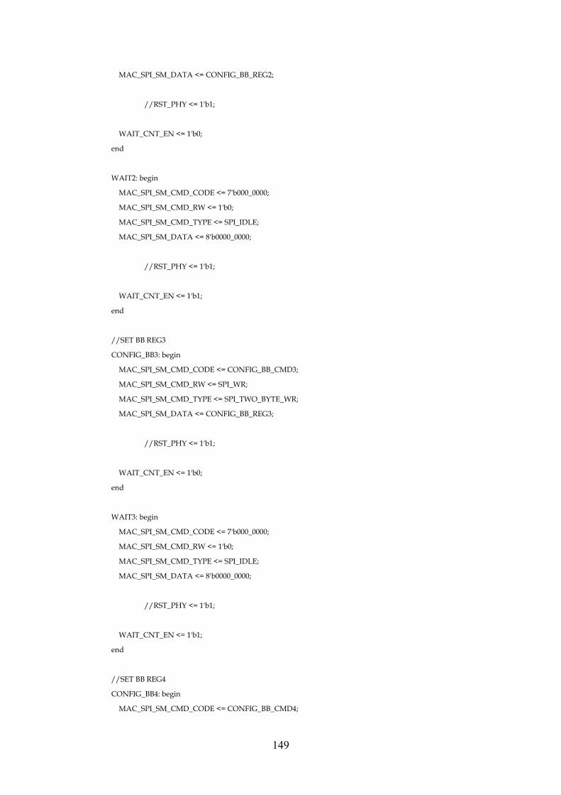
149
MAC_SPI_SM_DATA <= CONFIG_BB_REG2;
//RST_PHY <= 1'b1;
WAIT_CNT_EN <= 1'b0;
end
WAIT2: begin
MAC_SPI_SM_CMD_CODE <= 7'b000_0000;
MAC_SPI_SM_CMD_RW <= 1'b0;
MAC_SPI_SM_CMD_TYPE <= SPI_IDLE;
MAC_SPI_SM_DATA <= 8'b0000_0000;
//RST_PHY <= 1'b1;
WAIT_CNT_EN <= 1'b1;
end
//SET BB REG3
CONFIG_BB3: begin
MAC_SPI_SM_CMD_CODE <= CONFIG_BB_CMD3;
MAC_SPI_SM_CMD_RW <= SPI_WR;
MAC_SPI_SM_CMD_TYPE <= SPI_TWO_BYTE_WR;
MAC_SPI_SM_DATA <= CONFIG_BB_REG3;
//RST_PHY <= 1'b1;
WAIT_CNT_EN <= 1'b0;
end
WAIT3: begin
MAC_SPI_SM_CMD_CODE <= 7'b000_0000;
MAC_SPI_SM_CMD_RW <= 1'b0;
MAC_SPI_SM_CMD_TYPE <= SPI_IDLE;
MAC_SPI_SM_DATA <= 8'b0000_0000;
//RST_PHY <= 1'b1;
WAIT_CNT_EN <= 1'b1;
end
//SET BB REG4
CONFIG_BB4: begin
MAC_SPI_SM_CMD_CODE <= CONFIG_BB_CMD4;
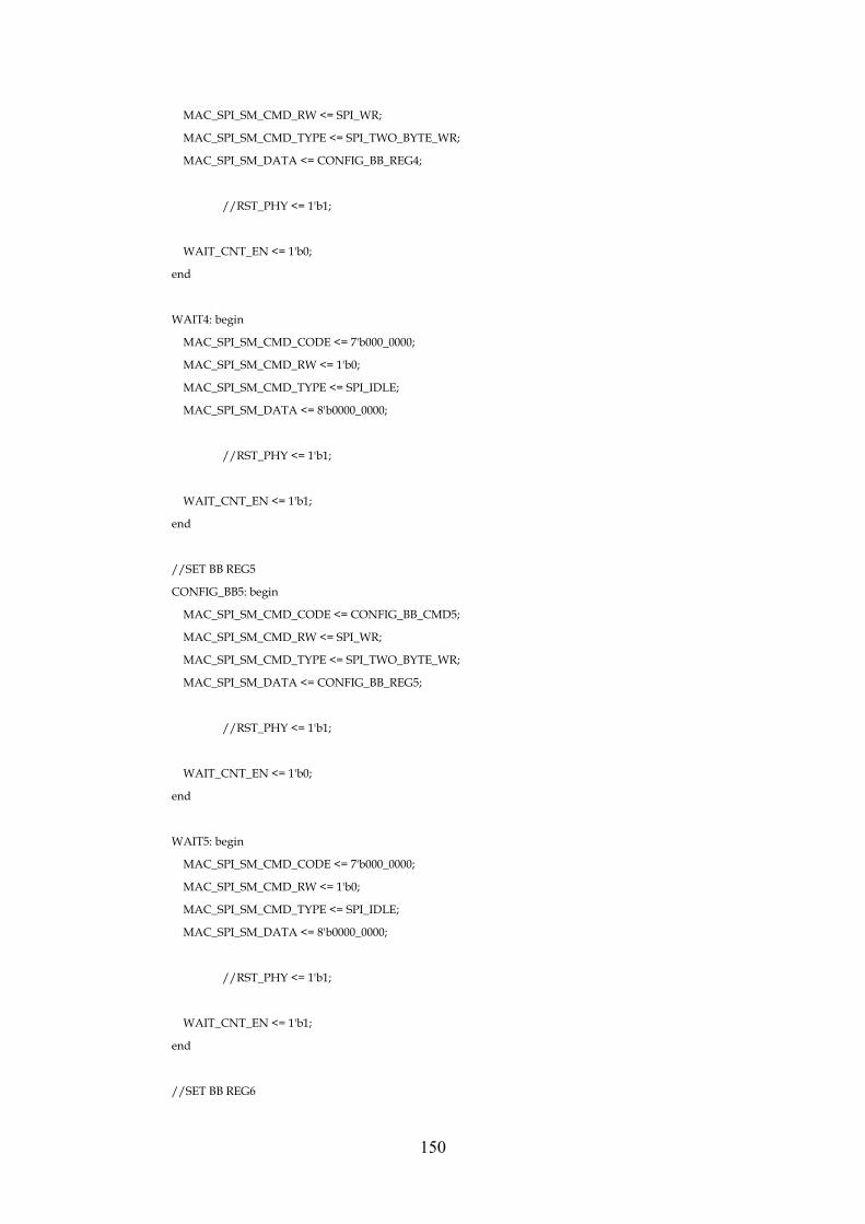
150
MAC_SPI_SM_CMD_RW <= SPI_WR;
MAC_SPI_SM_CMD_TYPE <= SPI_TWO_BYTE_WR;
MAC_SPI_SM_DATA <= CONFIG_BB_REG4;
//RST_PHY <= 1'b1;
WAIT_CNT_EN <= 1'b0;
end
WAIT4: begin
MAC_SPI_SM_CMD_CODE <= 7'b000_0000;
MAC_SPI_SM_CMD_RW <= 1'b0;
MAC_SPI_SM_CMD_TYPE <= SPI_IDLE;
MAC_SPI_SM_DATA <= 8'b0000_0000;
//RST_PHY <= 1'b1;
WAIT_CNT_EN <= 1'b1;
end
//SET BB REG5
CONFIG_BB5: begin
MAC_SPI_SM_CMD_CODE <= CONFIG_BB_CMD5;
MAC_SPI_SM_CMD_RW <= SPI_WR;
MAC_SPI_SM_CMD_TYPE <= SPI_TWO_BYTE_WR;
MAC_SPI_SM_DATA <= CONFIG_BB_REG5;
//RST_PHY <= 1'b1;
WAIT_CNT_EN <= 1'b0;
end
WAIT5: begin
MAC_SPI_SM_CMD_CODE <= 7'b000_0000;
MAC_SPI_SM_CMD_RW <= 1'b0;
MAC_SPI_SM_CMD_TYPE <= SPI_IDLE;
MAC_SPI_SM_DATA <= 8'b0000_0000;
//RST_PHY <= 1'b1;
WAIT_CNT_EN <= 1'b1;
end
//SET BB REG6
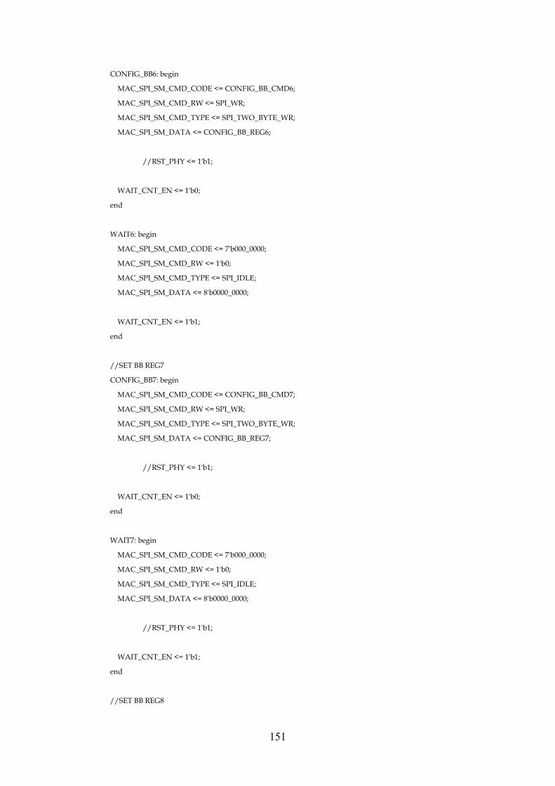
151
CONFIG_BB6: begin
MAC_SPI_SM_CMD_CODE <= CONFIG_BB_CMD6;
MAC_SPI_SM_CMD_RW <= SPI_WR;
MAC_SPI_SM_CMD_TYPE <= SPI_TWO_BYTE_WR;
MAC_SPI_SM_DATA <= CONFIG_BB_REG6;
//RST_PHY <= 1'b1;
WAIT_CNT_EN <= 1'b0;
end
WAIT6: begin
MAC_SPI_SM_CMD_CODE <= 7'b000_0000;
MAC_SPI_SM_CMD_RW <= 1'b0;
MAC_SPI_SM_CMD_TYPE <= SPI_IDLE;
MAC_SPI_SM_DATA <= 8'b0000_0000;
WAIT_CNT_EN <= 1'b1;
end
//SET BB REG7
CONFIG_BB7: begin
MAC_SPI_SM_CMD_CODE <= CONFIG_BB_CMD7;
MAC_SPI_SM_CMD_RW <= SPI_WR;
MAC_SPI_SM_CMD_TYPE <= SPI_TWO_BYTE_WR;
MAC_SPI_SM_DATA <= CONFIG_BB_REG7;
//RST_PHY <= 1'b1;
WAIT_CNT_EN <= 1'b0;
end
WAIT7: begin
MAC_SPI_SM_CMD_CODE <= 7'b000_0000;
MAC_SPI_SM_CMD_RW <= 1'b0;
MAC_SPI_SM_CMD_TYPE <= SPI_IDLE;
MAC_SPI_SM_DATA <= 8'b0000_0000;
//RST_PHY <= 1'b1;
WAIT_CNT_EN <= 1'b1;
end
//SET BB REG8
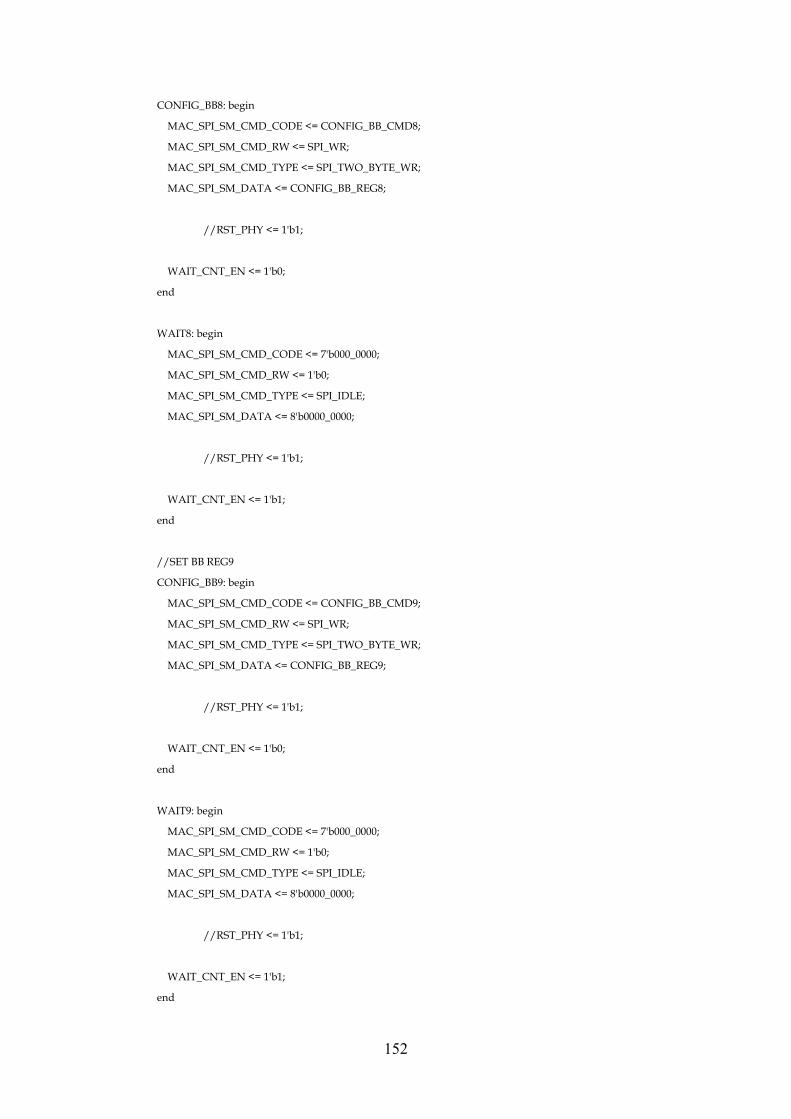
152
CONFIG_BB8: begin
MAC_SPI_SM_CMD_CODE <= CONFIG_BB_CMD8;
MAC_SPI_SM_CMD_RW <= SPI_WR;
MAC_SPI_SM_CMD_TYPE <= SPI_TWO_BYTE_WR;
MAC_SPI_SM_DATA <= CONFIG_BB_REG8;
//RST_PHY <= 1'b1;
WAIT_CNT_EN <= 1'b0;
end
WAIT8: begin
MAC_SPI_SM_CMD_CODE <= 7'b000_0000;
MAC_SPI_SM_CMD_RW <= 1'b0;
MAC_SPI_SM_CMD_TYPE <= SPI_IDLE;
MAC_SPI_SM_DATA <= 8'b0000_0000;
//RST_PHY <= 1'b1;
WAIT_CNT_EN <= 1'b1;
end
//SET BB REG9
CONFIG_BB9: begin
MAC_SPI_SM_CMD_CODE <= CONFIG_BB_CMD9;
MAC_SPI_SM_CMD_RW <= SPI_WR;
MAC_SPI_SM_CMD_TYPE <= SPI_TWO_BYTE_WR;
MAC_SPI_SM_DATA <= CONFIG_BB_REG9;
//RST_PHY <= 1'b1;
WAIT_CNT_EN <= 1'b0;
end
WAIT9: begin
MAC_SPI_SM_CMD_CODE <= 7'b000_0000;
MAC_SPI_SM_CMD_RW <= 1'b0;
MAC_SPI_SM_CMD_TYPE <= SPI_IDLE;
MAC_SPI_SM_DATA <= 8'b0000_0000;
//RST_PHY <= 1'b1;
WAIT_CNT_EN <= 1'b1;
end
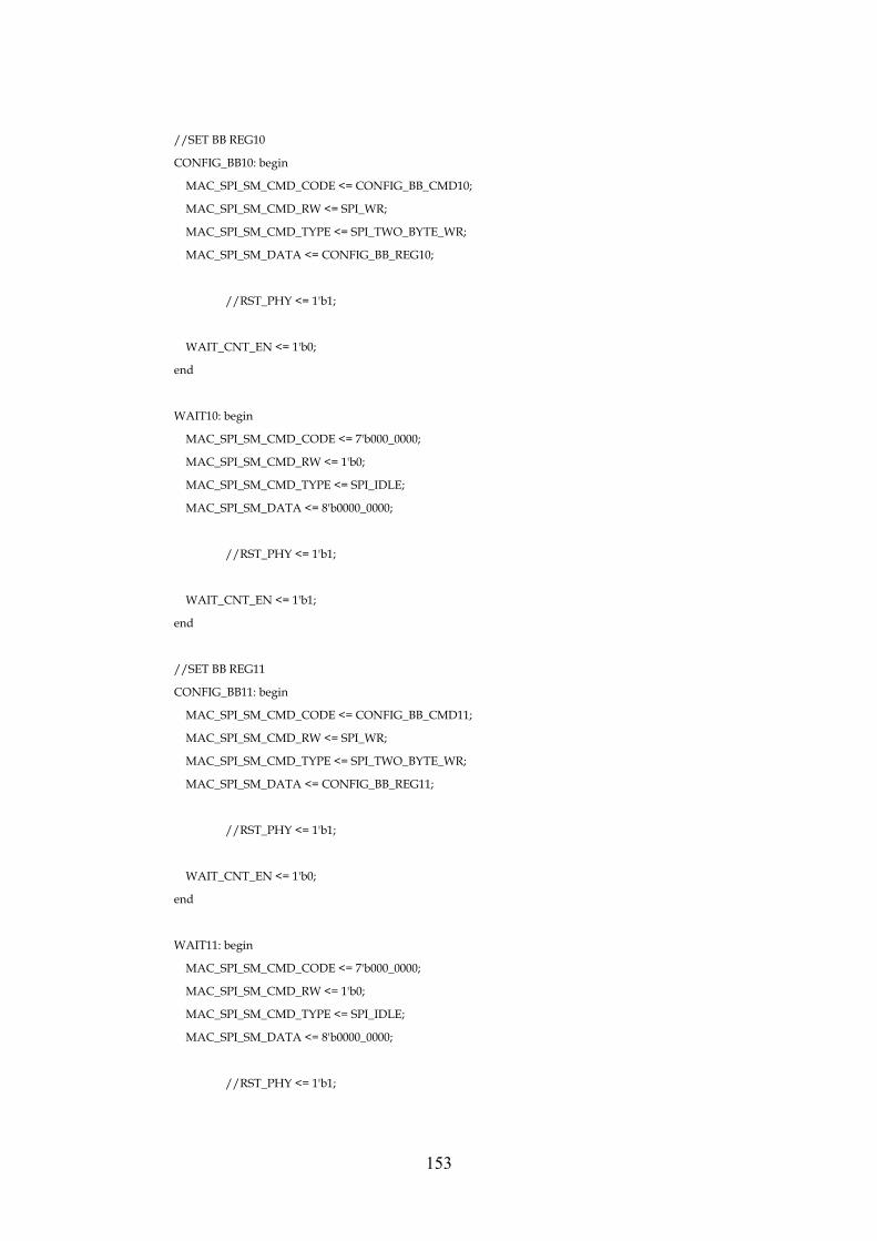
153
//SET BB REG10
CONFIG_BB10: begin
MAC_SPI_SM_CMD_CODE <= CONFIG_BB_CMD10;
MAC_SPI_SM_CMD_RW <= SPI_WR;
MAC_SPI_SM_CMD_TYPE <= SPI_TWO_BYTE_WR;
MAC_SPI_SM_DATA <= CONFIG_BB_REG10;
//RST_PHY <= 1'b1;
WAIT_CNT_EN <= 1'b0;
end
WAIT10: begin
MAC_SPI_SM_CMD_CODE <= 7'b000_0000;
MAC_SPI_SM_CMD_RW <= 1'b0;
MAC_SPI_SM_CMD_TYPE <= SPI_IDLE;
MAC_SPI_SM_DATA <= 8'b0000_0000;
//RST_PHY <= 1'b1;
WAIT_CNT_EN <= 1'b1;
end
//SET BB REG11
CONFIG_BB11: begin
MAC_SPI_SM_CMD_CODE <= CONFIG_BB_CMD11;
MAC_SPI_SM_CMD_RW <= SPI_WR;
MAC_SPI_SM_CMD_TYPE <= SPI_TWO_BYTE_WR;
MAC_SPI_SM_DATA <= CONFIG_BB_REG11;
//RST_PHY <= 1'b1;
WAIT_CNT_EN <= 1'b0;
end
WAIT11: begin
MAC_SPI_SM_CMD_CODE <= 7'b000_0000;
MAC_SPI_SM_CMD_RW <= 1'b0;
MAC_SPI_SM_CMD_TYPE <= SPI_IDLE;
MAC_SPI_SM_DATA <= 8'b0000_0000;
//RST_PHY <= 1'b1;

154
WAIT_CNT_EN <= 1'b1;
end
//SET BB REG12
CONFIG_BB12: begin
MAC_SPI_SM_CMD_CODE <= CONFIG_BB_CMD12;
MAC_SPI_SM_CMD_RW <= SPI_WR;
MAC_SPI_SM_CMD_TYPE <= SPI_TWO_BYTE_WR;
MAC_SPI_SM_DATA <= CONFIG_BB_REG12;
//RST_PHY <= 1'b1;
WAIT_CNT_EN <= 1'b0;
end
WAIT12: begin
MAC_SPI_SM_CMD_CODE <= 7'b000_0000;
MAC_SPI_SM_CMD_RW <= 1'b0;
MAC_SPI_SM_CMD_TYPE <= SPI_IDLE;
MAC_SPI_SM_DATA <= 8'b0000_0000;
//RST_PHY <= 1'b1;
WAIT_CNT_EN <= 1'b1;
end
/////////////////////////
//END OF BB RF&PHY INIT
/////////////////////////
//SET_SRXON
SET_SRXON: begin
MAC_SPI_SM_CMD_CODE <= SRXON;
MAC_SPI_SM_CMD_RW <= SPI_WR;
MAC_SPI_SM_CMD_TYPE <= SPI_ONE_BYTE_CMD;
MAC_SPI_SM_DATA <= SRXON_REG;
//RST_PHY <= 1'b1;
WAIT_CNT_EN <= 1'b0;
end
//Poll interruption bit
POLL_IRQ: begin
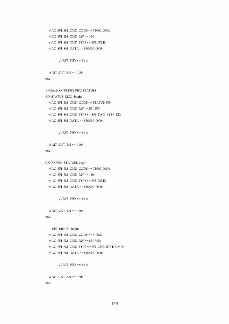
155
MAC_SPI_SM_CMD_CODE <= 7'b000_0000;
MAC_SPI_SM_CMD_RW <= 1'b0;
MAC_SPI_SM_CMD_TYPE <= SPI_IDLE;
MAC_SPI_SM_DATA <= 8'b0000_0000;
//RST_PHY <= 1'b1;
WAIT_CNT_EN <= 1'b0;
end
//Check RX BB PHY FIFO STATUS1
RD_STATUS_REG1: begin
MAC_SPI_SM_CMD_CODE <= STATUS_RD;
MAC_SPI_SM_CMD_RW <= SPI_RD;
MAC_SPI_SM_CMD_TYPE <= SPI_TWO_BYTE_RD;
MAC_SPI_SM_DATA <= 8'b0000_0000;
//RST_PHY <= 1'b1;
WAIT_CNT_EN <= 1'b0;
end
CK_RXFIFO_STATUS1: begin
MAC_SPI_SM_CMD_CODE <= 7'b000_0000;
MAC_SPI_SM_CMD_RW <= 1'b0;
MAC_SPI_SM_CMD_TYPE <= SPI_IDLE;
MAC_SPI_SM_DATA <= 8'b0000_0000;
//RST_PHY <= 1'b1;
WAIT_CNT_EN <= 1'b0;
end
SET_SIDLE1: begin
MAC_SPI_SM_CMD_CODE <= SIDLE;
MAC_SPI_SM_CMD_RW <= SPI_WR;
MAC_SPI_SM_CMD_TYPE <= SPI_ONE_BYTE_CMD;
MAC_SPI_SM_DATA <= 8'b0000_0000;
//RST_PHY <= 1'b1;
WAIT_CNT_EN <= 1'b0;
end
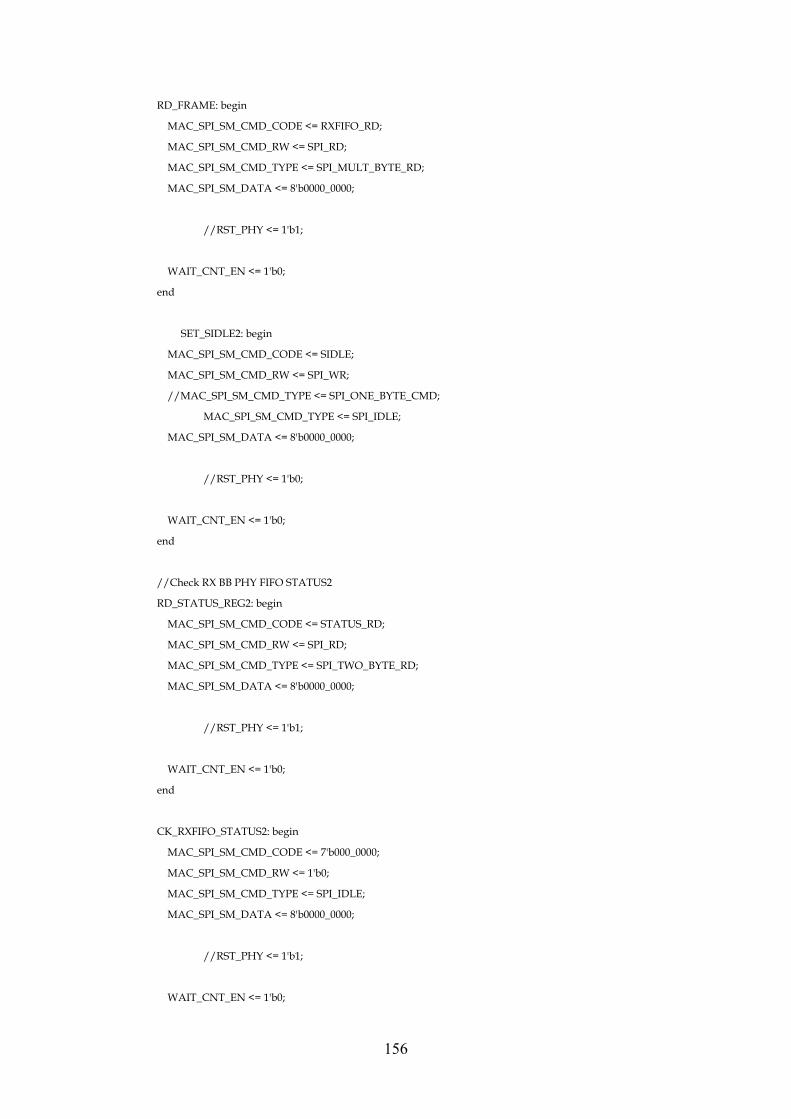
156
RD_FRAME: begin
MAC_SPI_SM_CMD_CODE <= RXFIFO_RD;
MAC_SPI_SM_CMD_RW <= SPI_RD;
MAC_SPI_SM_CMD_TYPE <= SPI_MULT_BYTE_RD;
MAC_SPI_SM_DATA <= 8'b0000_0000;
//RST_PHY <= 1'b1;
WAIT_CNT_EN <= 1'b0;
end
SET_SIDLE2: begin
MAC_SPI_SM_CMD_CODE <= SIDLE;
MAC_SPI_SM_CMD_RW <= SPI_WR;
//MAC_SPI_SM_CMD_TYPE <= SPI_ONE_BYTE_CMD;
MAC_SPI_SM_CMD_TYPE <= SPI_IDLE;
MAC_SPI_SM_DATA <= 8'b0000_0000;
//RST_PHY <= 1'b0;
WAIT_CNT_EN <= 1'b0;
end
//Check RX BB PHY FIFO STATUS2
RD_STATUS_REG2: begin
MAC_SPI_SM_CMD_CODE <= STATUS_RD;
MAC_SPI_SM_CMD_RW <= SPI_RD;
MAC_SPI_SM_CMD_TYPE <= SPI_TWO_BYTE_RD;
MAC_SPI_SM_DATA <= 8'b0000_0000;
//RST_PHY <= 1'b1;
WAIT_CNT_EN <= 1'b0;
end
CK_RXFIFO_STATUS2: begin
MAC_SPI_SM_CMD_CODE <= 7'b000_0000;
MAC_SPI_SM_CMD_RW <= 1'b0;
MAC_SPI_SM_CMD_TYPE <= SPI_IDLE;
MAC_SPI_SM_DATA <= 8'b0000_0000;
//RST_PHY <= 1'b1;
WAIT_CNT_EN <= 1'b0;
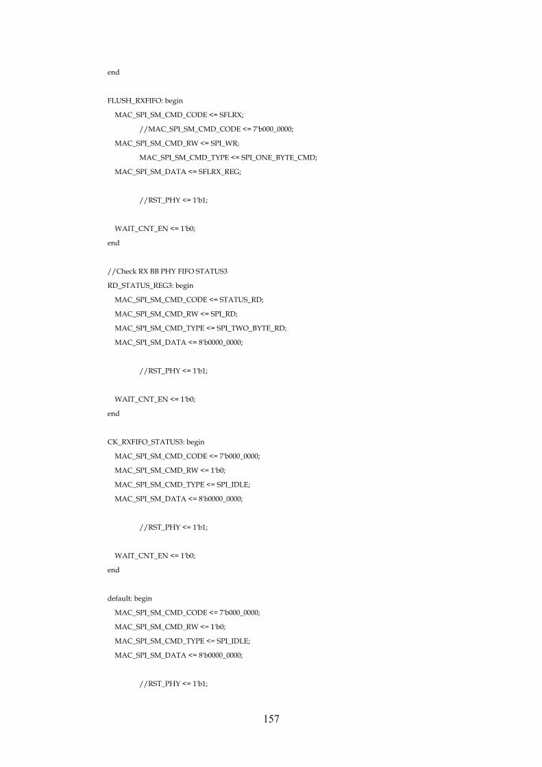
157
end
FLUSH_RXFIFO: begin
MAC_SPI_SM_CMD_CODE <= SFLRX;
//MAC_SPI_SM_CMD_CODE <= 7'b000_0000;
MAC_SPI_SM_CMD_RW <= SPI_WR;
MAC_SPI_SM_CMD_TYPE <= SPI_ONE_BYTE_CMD;
MAC_SPI_SM_DATA <= SFLRX_REG;
//RST_PHY <= 1'b1;
WAIT_CNT_EN <= 1'b0;
end
//Check RX BB PHY FIFO STATUS3
RD_STATUS_REG3: begin
MAC_SPI_SM_CMD_CODE <= STATUS_RD;
MAC_SPI_SM_CMD_RW <= SPI_RD;
MAC_SPI_SM_CMD_TYPE <= SPI_TWO_BYTE_RD;
MAC_SPI_SM_DATA <= 8'b0000_0000;
//RST_PHY <= 1'b1;
WAIT_CNT_EN <= 1'b0;
end
CK_RXFIFO_STATUS3: begin
MAC_SPI_SM_CMD_CODE <= 7'b000_0000;
MAC_SPI_SM_CMD_RW <= 1'b0;
MAC_SPI_SM_CMD_TYPE <= SPI_IDLE;
MAC_SPI_SM_DATA <= 8'b0000_0000;
//RST_PHY <= 1'b1;
WAIT_CNT_EN <= 1'b0;
end
default: begin
MAC_SPI_SM_CMD_CODE <= 7'b000_0000;
MAC_SPI_SM_CMD_RW <= 1'b0;
MAC_SPI_SM_CMD_TYPE <= SPI_IDLE;
MAC_SPI_SM_DATA <= 8'b0000_0000;
//RST_PHY <= 1'b1;
158
WAIT_CNT_EN <= 1'b0;
end
endcase
end //output assignment
///////////////////////////
// CONGFIGURE WAIT COUNTER
///////////////////////////
always @(posedge MAC_SPI_SM_CLK or negedge MAC_SPI_SM_RSTN)
begin
if (~MAC_SPI_SM_RSTN)
CONFIG_WAIT_CNT <= 0;
else if (CONFIG_WAIT_CNT == WAIT_CYCLES)
CONFIG_WAIT_CNT <= 0;
else if (WAIT_CNT_EN == 1'b1)
CONFIG_WAIT_CNT <= CONFIG_WAIT_CNT + 1;
end
endmodule //BPRO_RX_BB_MAC_SPI_SM