Embed Size (px)
Citation preview

Design Guidelines For 78P235x
E4/STM1e LIUs
APPLICATION NOTE
Page 1 of 15 2008 Teridian Semiconductor Corp. Rev 2.1
A Maxim Integrated Products Brand
AUGUST 2008
APPLICATION NOTE CONTENTS Introduction to TERIDIAN 78P235x LIUs Layout Guidelines Recommended I/O Terminations Transformers Supplemental Surge Protection Return Loss Matching Circuit (optional) Coaxial Connectors Crystal Oscillator Requirements Thermally Enhanced LQFPs E4 Reference Design Sample Jitter and Pulse Mask Test Results
APPLICABLE DEVICES 78P2352 Dual Channel LIU 78P2351 Single Channel LIU 78P2351R Small form factor LIU
INTRODUCTION TO TERIDIAN 78P235x LIUs The TERIDIAN 78P235x STM1e/E4 Line Interface Units (LIU) ICs are TERIDIAN’s second-generation design. Next generation design architectures and techniques are used to provide system designers with enhanced functionality, performance and improved noise immunity. On the receiver side, one such technique is the use of a digital PLL, rather than the traditional analog PLL. Note the absence of the external loop filter capacitor. Thanks to the digital PLL, this is now provided on chip. The removal of the pin and external connection for this critical node eliminates EMI, a noise injection port, and significantly improves the noise immunity. Additionally, since the loop damping is controlled on chip and is digital, the 0.1dB jitter peaking specification is now guaranteed by the digital loop filter. Traditionally, an external 1% resistor is used to set the transmitter amplitude, and sometimes used in setting internal biasing. Thus, the pin can be a source of EMI pickup directly into critical blocks of the device. On this generation design, this external resistor and pin have been removed and placed internally, thus completely eliminating the potential for EMI interference. LAYOUT AND I/O TERMINATION GUIDELINES When designing an analog interface for error-free performance, there are several important factors to consider. This document provides a few recommendations that can help alleviate unwanted noise due to sub-optimal board layout around the LIU. It also provides general guidelines for meeting the stringent return loss and CMI transmit pulse shape requirements, both of which are largely dependant on PCB design and layout. GROUND PLANE A common system grounding approach is to use a different ground at the coax connectors for safety isolation and improved electromagnetic compatibility. In this implementation, the coax connector shield is directly connected to frame or chassis ground. The component ground is an isolated plane that connects directly to the negative supply pins of active components. These grounds are isolated from each other by placing a strip of area, which is void of copper, in the ground plane underneath the primary of the transformers as shown in Figure 1 below. The chassis/frame ground plane is directly connected to the equipment chassis, which connects to the facilities Earth ground structure. Reference ITU-T recommendation K.27 for more information on grounding recommendations.

Design Guidelines for TERIDIAN 78P235x LIUs
Page 2 of 15 2008 Teridian Semiconductor Corp. Rev 2.1
HINT: If experiencing long term bit errors in a design with isolated grounds, try connecting frame and supply grounds near the transformer with a strip of low inductance wire.
LIU
FRAMEGROUND
COMPONENTGROUND
COPPER VOID
Figure 1. Two different ground planes
SUPPLY (VCC) PLANE As with the component ground plane, the power plane layer should only extend to the LIU side of the transformer. The outer edge of the power plane should be kept 10 mils short of the ground plane’s outer edge to avoid plane-to-plane current fringing at the plane edges.
DECOUPLING Decoupling (bypass) capacitors are used to short high frequency noise and switching transients from supply to the ground plane. Two decades of caps are recommended, e.g. a mix of 0.1uF and 0.001uF, in order to provide broader bypass bandwidth. A 0603 size bypass cap, with via as close as possible to it’s pads will provide a minimal lead inductance, further enhancing the effectiveness of the bypass. Layout the bypass caps close to the 78P235x, preferably under the component on the bottom side. Ceramic, low ESR caps are recommended for best frequency response. Generally X7R dielectric capacitors provide the best price/performance trade-off.

Design Guidelines for TERIDIAN 78P235x LIUs
Page 3 of 15 2008 Teridian Semiconductor Corp. Rev 2.1
ANALOG SIGNAL TRACES AND TERMINATIONS The 78P235x LIUs have differential drivers and receivers. To maintain signal integrity and optimal performance, all differential traces should be of equal length, parallel to each other, and as short as possible. The impedance of such traces and terminations should also be well controlled. For the Reset pin (PORB), do not tie directly to VCC as this will prevent internal power-on reset. Connect to a microcontroller for manual reset or de-couple to ground using a 1nF capacitor.
Each LVPECL interface should have a differential trace impedance of 100Ω to the SerDes. For best return loss, the input termination resistors should be placed within one inch of their 78P235x input pins. LVPECL output drivers require an external pull-down resistor, which should also be placed near the output pin. See Figure 2 and Figure 3 for diagrams of recommended terminations of LVPECL I/Os.
NOTES: 1. For DC-coupling, the common mode or bias voltage levels of both ICs must be compatible. Reference product
specifications for more information on bias levels or AC-couple.
2. For E4 applications, DC coupling is required due to the unframed nature of AIS (all ones) signaling in E4.
LVPECL Output (PO)
from circuit
VCC
from circuit
VCC 170
170
50 ohm
50 ohm
to LVPECLinput
< 1"
< 1"
< 20"20
20
Reff
235x IC PCB Figure 2: LVPECL Outputs
LVPECL Input (PI)
to gates
to gates
100
50 ohm
50 ohm
< 1"
< 1"
fromtransmitting
chip
82
50 ohm
50 ohmfrom
transmittingchip
3.3V
82
170 170
PCB 235x ICPCB 235x IC
Figure 3: LVPECL Inputs (DC-coupled and 0.1uF AC-coupled options)

Design Guidelines for TERIDIAN 78P235x LIUs
Page 4 of 15 2008 Teridian Semiconductor Corp. Rev 2.1
All CMI coded (Analog) differential pair signal routes should have a differential trace impedance of 75Ω
The transmit and receive ‘Tip’ (on primary side of transformer) should be a
between the 78P235x IC and the transformer. The termination resistors need to be placed as close as possible, and within one inch, of their 78P235x pins to optimize transmit pulse shaping and minimize reflections.
75Ω single-ended trace
Unlike the CMI Receiver, the Transmitter requires external biasing. Figure 5 shows two methods for biasing the transmit driver. Biasing the transmit path at the transformer center tap with a single 75Ω termination resistor uses the fewest components, but is only recommended when the transformer placement can be near the LIU.
to the coax connector. The coax shield or ‘Ring’ should be directly connected to the frame or chassis ground plane. The quality of this ground connection is critical for ESD Immunity at the faceplate and EMC performance.
The alternate (and preferred) method is to bias the transmit path between the 2 termination resistors minimizing the path and inductance from Vcc to the internal current sink. The value of each resistor should equal to one half of the total termination used for the pair, so that each half of the signal is seeing the correct termination value (37.5Ω). The decoupling capacitor value should be 0.1uF (or a combination of 0.01uF and 0.1uF).
2.1V
10k
10k
RXxP
RXxN
to gates
to gates
75
37.5 ohm
37.5 ohm75 ohmTIP
RING
< 1"RX CMI Input
PCB 235x IC
Figure 4: CMI Receiver
fromcircuit
CMIxP
CMIxN
75
37.5 ohm
37.5 ohm
VCC
75 ohmTIP
RING
TX CMI Output(Transformer Bias)
< 1"
26mA
0.1uF
PCB 235x IC
fromcircuit
CMIxP
CMIxN
37.537.5 ohm
37.5 ohm
VCC
75 ohmTIP
RING
TX CMI Output(Resistor Bias)
< 1"
26mA
PCB 235x IC
37.5
0.1uF
Figure 5: CMI Transmitter (Transformer and Resistor Biasing options)
Design Guidelines for TERIDIAN 78P235x LIUs
Page 5 of 15 2008 Teridian Semiconductor Corp. Rev 2.1
DIGITAL TRACES AND TERMINATIONS Common board design practices should be applied in the routing of high-speed clock traces. Preferably keep these signals on the top layer and their length comparable to their associated data path. Its also good practice to keep clock routes away from the analog side of the LIU as well as it’s associated analog signal routes. Series source termination is recommended on the parallel (nibble) interface and single-ended clocks. The termination resistor is placed close to the source driver device. The impedance of the termination resistor, in combination with the AC output impedance of the source driver, should match the associated trace impedance. Note the output impedance of the LIU is about 30Ω. The LIU source series termination for a 75Ω trace should therefore be about 45Ω. This is only appropriate however for a single point to point route, since ideal signal characteristics only appear at the end point of the signal route. Series termination must not be used for multi-destination clock routes. External clock distribution buffers or parallel termination should be used for multi-destination clock routes.
from circuit
< 2"
75 ohm40 toreceiving
chip
CMOS Digital Output (CO,COZ)
< 40"
30
Rsrc
235x IC PCB
Figure 6: CMOS Outputs
CMOS Digital Input (CI,CIT,CID)75 ohm Type CI
Type CID
10k
Type CIT
to gates
10k
10k
VCC
75 ohm
75 ohm
< 2"
< 2"
< 2"
fromtransmitting
chipto gates
to gates
PCB 235x IC
Figure 7: CMOS Inputs

Design Guidelines for TERIDIAN 78P235x LIUs
Page 6 of 15 2008 Teridian Semiconductor Corp. Rev 2.1
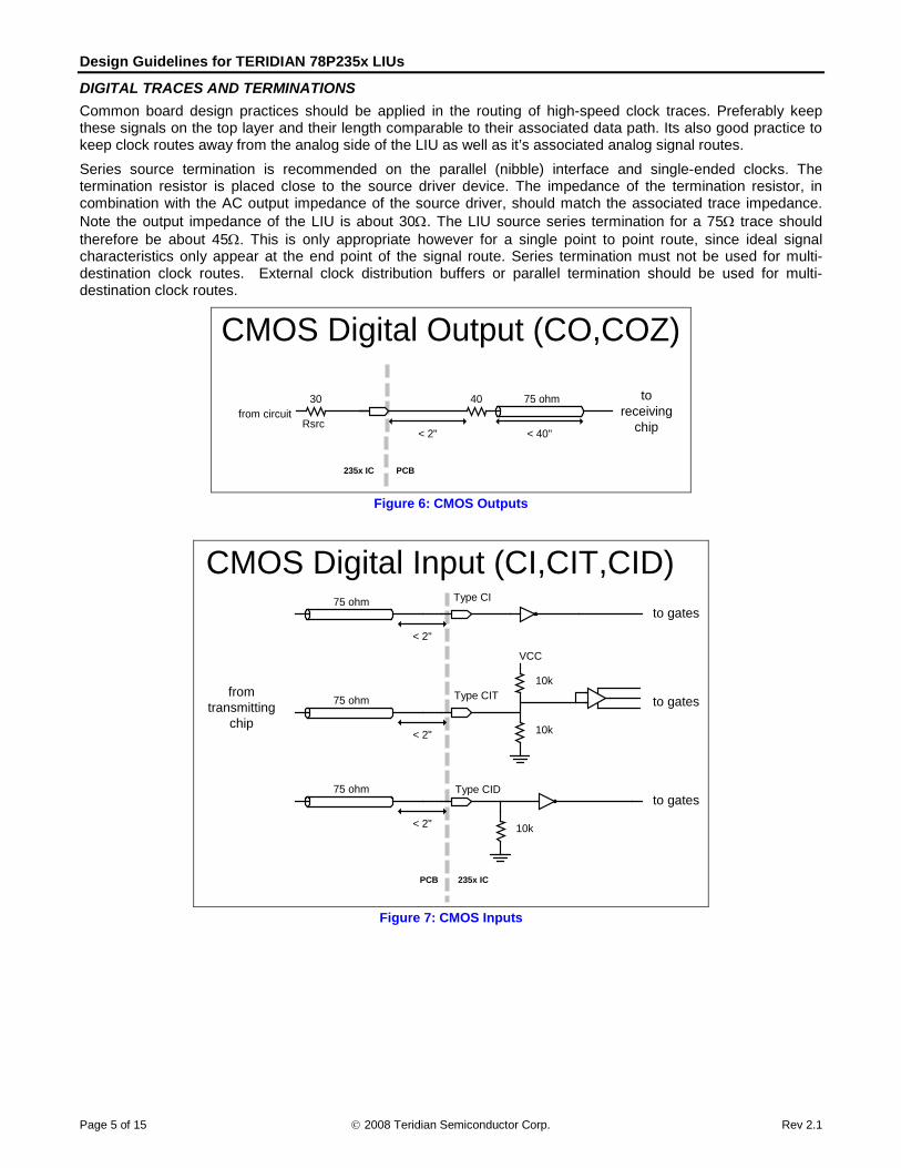
TRANSFORMER SELECTION The 78P235x LIUs use 1:1CT (center-tapped) wide band transformers for both transmit and receive ports. These wideband transformers must exhibit the following characteristics: 75Ω impedance (primary and secondary) Max RF power: ~250mA Max DC current: ~30mA Avg. Insertion loss: 1dB max Return loss: Min 16dB (7 –250 MHz) Frequency Response:
The bandwidth or frequency response of available transformers can range from 400MHz to 800MHz. For some system environments, more bandwidth-limiting transformers can help eliminate the overshoots that can cause pulse mask failures. Too narrow of a bandwidth will result in a rounded transmit pulse shape and receiver sensitivity to binary CMI zeroes at max cable loss.
To provide system designers with greater flexibility, Teridian has evaluated and approved multiple vendors in compatible SMT footprints. The following table lists the recommended single and dual transformers from different vendors.
NOTES:
1. To request test data on any of the listed transformers or to get an updated list of qualified vendors, please send an email to: [email protected]
2. Pinout naming conventions can vary from vendor to vendor, but all winding diagrams should match those found in Figure 9.
Single core transformers
Manufacturer Part Number Mini Circuit ADT1-1WT-1
Halo TG04-TDK2NS
Tamura TTC-298
Midcom 7400-30R-LF1
Datatronic SM78809
Dual core transformers Manufacturer Part Number Halo TG04-TDK1N1
TAMURA TTC-300
Midcom 000-7419-30R-LF1
Design Guidelines for TERIDIAN 78P235x LIUs
Page 7 of 15 2008 Teridian Semiconductor Corp. Rev 2.1
Figure 9. Single and Dual Core Transformer Diagrams (top view)
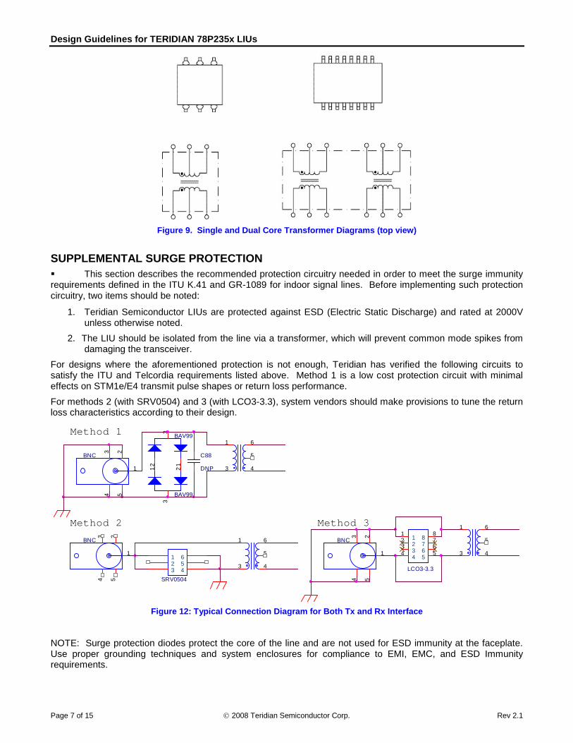
SUPPLEMENTAL SURGE PROTECTION This section describes the recommended protection circuitry needed in order to meet the surge immunity requirements defined in the ITU K.41 and GR-1089 for indoor signal lines. Before implementing such protection circuitry, two items should be noted:
1. Teridian Semiconductor LIUs are protected against ESD (Electric Static Discharge) and rated at 2000V unless otherwise noted.
2. The LIU should be isolated from the line via a transformer, which will prevent common mode spikes from damaging the transceiver.
For designs where the aforementioned protection is not enough, Teridian has verified the following circuits to satisfy the ITU and Telcordia requirements listed above. Method 1 is a low cost protection circuit with minimal effects on STM1e/E4 transmit pulse shapes or return loss performance. For methods 2 (with SRV0504) and 3 (with LCO3-3.3), system vendors should make provisions to tune the return loss characteristics according to their design.
Method 1
3 4
5
1 6
SRV0504
123 4
56
BNC
1
234 5
Method 3
BAV99
3
12
Method 2
3 4
5
1 6
3 4
5
1 6
LCO3-3.3
1234 5
678
1234 5
678BNC
1
234 5
BAV99
3
1 2
C88
DNP
BNC
1
234 5
Figure 12: Typical Connection Diagram for Both Tx and Rx Interface
NOTE: Surge protection diodes protect the core of the line and are not used for ESD immunity at the faceplate. Use proper grounding techniques and system enclosures for compliance to EMI, EMC, and ESD Immunity requirements.

Design Guidelines for TERIDIAN 78P235x LIUs
Page 8 of 15 2008 Teridian Semiconductor Corp. Rev 2.1
RETURN LOSS MATCHING CIRCUIT Meeting the 15dB return loss requirements at the CMI-coded coax ports often requires a significant amount of engineering hours due to the unique impedance characteristics of each system design, particularly at frequencies above 200MHz. Return loss is a parameter that can only be measured at the system level. Evaluating any individual component’s return loss won’t be efficient and will provide misleading results. For challenging environments where the coax connector, transformer, and LIU are not located near each other or even on the same card, a flexible termination scheme is required to meet the return loss performance for both transmit and receive paths. The diagram in Figure 8 below shows a suggested circuit to optimize the impedance on the transmission lines by adding discrete component footprints right near the transformers in the differential paths. The capacitance (C) and inductance (L) values are unique for each design and will generally be in the range of a few nH or pF.
L
R 75
BAV99
R 75
VCC
C
75
R 75
BNC
BNC
BAV99
L
L
75 R 75
L
BAV99
C
75
0.1uF
T1 Transformer Dual CT
C
To LIU
C
BAV99
Figure 8. (Optional) Discrete components to improve the return loss

Design Guidelines for TERIDIAN 78P235x LIUs
Page 9 of 15 2008 Teridian Semiconductor Corp. Rev 2.1
COAXIAL CONNECTORS Coaxial connectors must be of the 75-ohm variant to avoid compromising the mechanical properties of the mating receptacle and to match the impedance of the line. For optimal EMC performance and ESD immunity at the faceplate, it is critical that the shield of the coax connectors be well bonded to the frame or chassis in any board design. The system enclosure should also be properly grounded at the earth facility. For optimal space savings, Teridian suggests the use of 75 ohm DIN 1.0/2.3 connectors (BT Type 54), which can be sourced from the following suppliers.
• Xian Connector • Compel • Radiall • SIAM • Amphenol • Tekmos • Tru • AMP / Tyco • Hsu-Tsan Group
CRYSTAL OSCILLATOR REQUIREMENTS The following requirements are provided with the assumption that plesiochronous transmit timing mode is enabled. If using a crystal oscillator in any of the synchronous modes, the clock stability over the life of the oscillator will be inherently limited by the SONET/SDH/PDH bit rate requirements of +/- 20ppm for STS-3/STM-1 and +/-15ppm for E4. Several factors to consider when selecting a crystal oscillator for plesiochronous mode:
Frequency tolerance / stability (70ppm or better) Aging (not to exceed 100ppm over life) Rise / Fall time Output amplitude (must be at least 2V signal swing) Period jitter (up to 220ps evaluated without any appreciable effects)
Evaluation of the following crystal oscillators at Teridian showed no appreciable differences in jitter performance.
Vendor Part number CTS CB3LV-3C-19.440000
Ecliptek EH2645ETTS-19.440M
SaRonix S1613B-19.44
Abracon ASV-19.44MHz-C
Crystek C3392-19.44MHz
Design Guidelines for TERIDIAN 78P235x LIUs
Page 10 of 15 2008 Teridian Semiconductor Corp. Rev 2.1
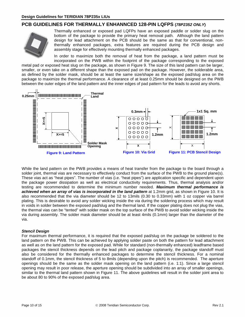
PCB GUIDELINES FOR THERMALLY ENHANNCED 128-PIN LQFPS (78P2352 ONLY) Thermally enhanced or exposed pad LQFPs have an exposed paddle or solder slug on the bottom of the package to provide the primary heat removal path. Although the land pattern design for lead attachment on the PCB should be the same as that for conventional, non-thermally enhanced packages, extra features are required during the PCB design and assembly stage for effectively mounting thermally enhanced packages. In order to maximize both the removal of heat from the package, a land pattern must be incorporated on the PWB within the footprint of the package corresponding to the exposed
metal pad or exposed heat slug on the package, as shown in Figure 9. The size of this land pattern can be larger, smaller, or even take on a different shape than the exposed pad on the package. However, the solderable area, as defined by the solder mask, should be at least the same size/shape as the exposed pad/slug area on the package to maximize the thermal performance. A clearance of at least 0.25mm should be designed on the PWB between the outer edges of the land pattern and the inner edges of pad pattern for the leads to avoid any shorts.
X>=5
ThermalLand
X>=5
0.25mm
Solder MaskOpening
Figure 9: Land Pattern
X
X
0.3mm
1.2mm
Figure 10: Via Grid
X
X
1.2mm
1x1 Sq. mm
Figure 11: PCB Stencil Design
While the land pattern on the PWB provides a means of heat transfer from the package to the board through a solder joint, thermal vias are necessary to effectively conduct from the surface of the PWB to the ground plane(s). These vias act as “heat pipes”. The number of vias (i.e. “heat pipes”) are application specific and dependent upon the package power dissipation as well as electrical conductivity requirements. Thus, thermal analysis and/or testing are recommended to determine the minimum number needed. Maximum thermal performance is achieved when an array of vias is incorporated in the land pattern at 1.2mm grid, as shown in Figure 10. It is also recommended that the via diameter should be 12 to 13mils (0.30 to 0.33mm) with 1 oz copper via barrel plating. This is desirable to avoid any solder wicking inside the via during the soldering process which may result in voids in solder between the exposed pad/slug and the thermal land. If the copper plating does not plug the vias, the thermal vias can be “tented” with solder mask on the top surface of the PWB to avoid solder wicking inside the via during assembly. The solder mask diameter should be at least 4mils (0.1mm) larger than the diameter of the via.
Stencil Design For maximum thermal performance, it is required that the exposed pad/slug on the package be soldered to the land pattern on the PWB. This can be achieved by applying solder paste on both the pattern for lead attachment as well as on the land pattern for the exposed pad. While for standard (non-thermally enhanced) leadframe based packages the stencil thickness depends on the lead pitch and package coplanarity, the package standoff must also be considered for the thermally enhanced packages to determine the stencil thickness. For a nominal standoff of 0.1mm, the stencil thickness of 5 to 8mils (depending upon the pitch) is recommended. The aperture openings should be the same as the solder mask opening on the land pattern (i.e. 1:1). Since a large stencil opening may result in poor release, the aperture opening should be subdivided into an array of smaller openings, similar to the thermal land pattern shown in Figure 11. The above guidelines will result in the solder joint area to be about 80 to 90% of the exposed pad/slug area.
Design Guidelines for TERIDIAN 78P235x LIUs
Page 11 of 15 2008 Teridian Semiconductor Corp. Rev 2.1
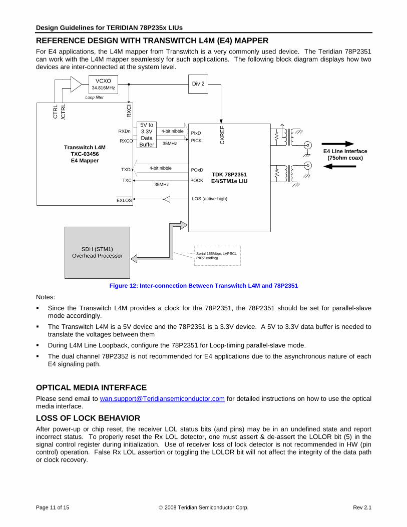
REFERENCE DESIGN WITH TRANSWITCH L4M (E4) MAPPER For E4 applications, the L4M mapper from Transwitch is a very commonly used device. The Teridian 78P2351 can work with the L4M mapper seamlessly for such applications. The following block diagram displays how two devices are inter-connected at the system level.
TDK 78P2351E4/STM1e LIU
SDH (STM1)Overhead Processor Serial 155Mbps LVPECL
(NRZ coding)
POxD
POCK
PICKPIxD
Transwitch L4MTXC-03456E4 Mapper
VCXO34.816MHz
RX
CI
CK
RE
F
TXDn
TXC
RXDn
RXCO
LOS (active-high)EXLOS
E4 Line Interface(75ohm coax)
Loop filter
CTR
L/C
TRL
Div 2
4-bit nibble5V to3.3VData
Buffer
4-bit nibble
35MHz
35MHz
Figure 12: Inter-connection Between Transwitch L4M and 78P2351
Notes: Since the Transwitch L4M provides a clock for the 78P2351, the 78P2351 should be set for parallel-slave
mode accordingly. The Transwitch L4M is a 5V device and the 78P2351 is a 3.3V device. A 5V to 3.3V data buffer is needed to
translate the voltages between them During L4M Line Loopback, configure the 78P2351 for Loop-timing parallel-slave mode. The dual channel 78P2352 is not recommended for E4 applications due to the asynchronous nature of each
E4 signaling path.
OPTICAL MEDIA INTERFACE Please send email to [email protected] for detailed instructions on how to use the optical media interface.
LOSS OF LOCK BEHAVIOR After power-up or chip reset, the receiver LOL status bits (and pins) may be in an undefined state and report incorrect status. To properly reset the Rx LOL detector, one must assert & de-assert the LOLOR bit (5) in the signal control register during initialization. Use of receiver loss of lock detector is not recommended in HW (pin control) operation. False Rx LOL assertion or toggling the LOLOR bit will not affect the integrity of the data path or clock recovery.

Design Guidelines for TERIDIAN 78P235x LIUs
Page 12 of 15 2008 Teridian Semiconductor Corp. Rev 2.1
SAMPLE JITTER TEST RESULTS Receive Jitter Tolerance
Jitter Transfer
Intrinsic Transmit Jitter STM-1e FIFO enabled FIFO bypassed (Plesiochronous timing mode) Filters on 0.025UIp-pk 0.049UIp-pk Filters off 0.053UIp-pk 0.049UIp-pk

Design Guidelines for TERIDIAN 78P235x LIUs
Page 13 of 15 2008 Teridian Semiconductor Corp. Rev 2.1
SAMPLE TRANSMIT PULSE SHAPE RESULTS There are generally two methods for specifying and measuring the transmit pulse signal integrity. Pulse Mask Templates originate from ITU-T G.703 and Eye Diagrams originate from ANSI T1-102. Telcordia GR-253-CORE refers to both and provides a better description on how to use the eye diagrams. Pulse Template The Pulse Template specifies the characteristics of singular pulses. It defines the precise shape of the pulse including rise time, fall time, amplitude and overshoot. It takes into account the affect of inter-symbol interference from successive pulses and reflection from improper terminations. To perform pulse template measurements, the oscilloscope must be able to isolate the pulse under evaluation, be it binary 1 or 0. The Tektronics TDS 784 is one oscilloscope that has the ability to trigger on CMI signals, capturing only the pulses of interest. The signal can be acquired using average or sample mode depending on the parameters to be evaluated. Average mode provides the clearest indication of pulse shape and allows measurement of continuous anomalies such as reflection and inter-symbol interference. Sample mode will provide information on spurious signal noise and occasional violations of the pulse template. As noted in G.703, it is important to eliminate the effects of low frequency jitter or wander when making pulse mask measurements. Therefore it is not recommended to use long persistent acquisition methods (DPO) for performing pulse template measurements.
Instrumentation Variations These measurements were taken on the Tektronics TDS 784D oscilloscope. Generally auto set will properly select the proper acquisition method and set time and voltage scales. However, often these settings come up incorrect and will need to be adjusted. Different scopes will default to different acquisition modes depending on model. It is important to carefully monitor all scope settings when performing pulse shape measurements.
Design Guidelines for TERIDIAN 78P235x LIUs
Page 14 of 15 2008 Teridian Semiconductor Corp. Rev 2.1
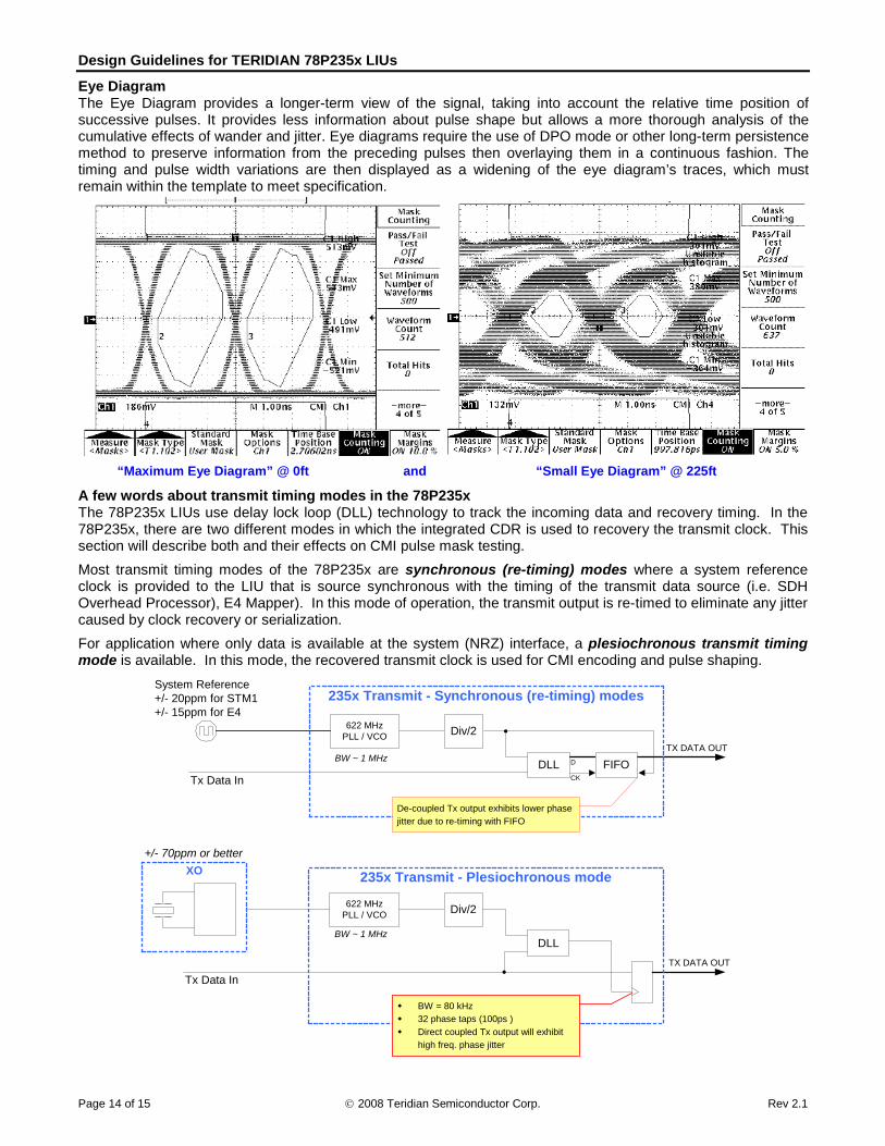
Eye Diagram The Eye Diagram provides a longer-term view of the signal, taking into account the relative time position of successive pulses. It provides less information about pulse shape but allows a more thorough analysis of the cumulative effects of wander and jitter. Eye diagrams require the use of DPO mode or other long-term persistence method to preserve information from the preceding pulses then overlaying them in a continuous fashion. The timing and pulse width variations are then displayed as a widening of the eye diagram’s traces, which must remain within the template to meet specification.
“Maximum Eye Diagram” @ 0ft and “Small Eye Diagram” @ 225ft
A few words about transmit timing modes in the 78P235x The 78P235x LIUs use delay lock loop (DLL) technology to track the incoming data and recovery timing. In the 78P235x, there are two different modes in which the integrated CDR is used to recovery the transmit clock. This section will describe both and their effects on CMI pulse mask testing. Most transmit timing modes of the 78P235x are synchronous (re-timing) modes where a system reference clock is provided to the LIU that is source synchronous with the timing of the transmit data source (i.e. SDH Overhead Processor), E4 Mapper). In this mode of operation, the transmit output is re-timed to eliminate any jitter caused by clock recovery or serialization. For application where only data is available at the system (NRZ) interface, a plesiochronous transmit timing mode is available. In this mode, the recovered transmit clock is used for CMI encoding and pulse shaping.
D
622 MHzPLL / VCO Div/2
DLL FIFOCK
TX DATA OUTBW ~ 1 MHz
235x Transmit - Synchronous (re-timing) modes
Tx Data In
System Reference+/- 20ppm for STM1+/- 15ppm for E4
De-coupled Tx output exhibits lower phasejitter due to re-timing with FIFO
622 MHzPLL / VCO Div/2
Tx Data In
DLL
XO
TX DATA OUT
BW ~ 1 MHz
235x Transmit - Plesiochronous mode
BW = 80 kHz 32 phase taps (100ps ) Direct coupled Tx output will exhibit
high freq. phase jitter
+/- 70ppm or better

Design Guidelines for TERIDIAN 78P235x LIUs
Page 15 of 15 2008 Teridian Semiconductor Corp. Rev 2.1
The DLLs use 32 phase taps to recover a 311MHz clock (nominal phase tap spacing is 100ps). With jitter of the incoming data and variable transition density, the recovered clock will naturally hop between a couple of taps even when phase locked. In plesiochronous timing mode, this will appear as high frequency phase jumps or phase jitter during isolated CMI pulse mask measurements (most noticeable with CMI binary 0) This jitter generation is normal and inherent to all CDR’s, although more linear with analog PLLs. The magnitude of the output jitter is directly related to the bandwidth of the Tx CDR which is 80kHz in the case of the 78P235x transmit CDR. It should be noted this jitter will not effect intrinsic jitter measurements when measured with standards filters enabled.
The two plots above show a close-in view of the peak-to-peak transmit phase jitter in plesiochronous (left) and synchronous modes (right). This is most noticeable on the falling edge of a CMI Binary 0 Pulse Template Measurement. It should be noted that every isolated pulse is still compliant to the Pulse Template requirements, but mask counting and infinite persistence results will vary from scope to scope depending on acquisition methods.
Be sure to center triggering position or amplitudes to avoid false failures on falling edge of CMI - Binary 0 pulse masks