Embed Size (px)
Citation preview

Application Note Please read the Important Notice and Warnings at the end of this document V X.Y
www.infineon.com page 1 of 33 2018-08-28
AN_1806_PL32_1808_171123
Design guide for low-noise transistors in FM
radio front ends
RF bipolar transistors
About this document
Scope and purpose
This application note provides application circuit design examples of Infineon’s low-noise bipolar silicon (Si) and silicon germanium: carbon (SiGe:C) transistors for FM radio applications. In this document, the transistor-
based low noise amplifier (LNA) schematics, PCB layouts and measurement results are presented. This document is relevant to the following low-noise transistors:
BFR340F FM antenna LNA for 76 to 108MHz
BFR460L3 FM antenna LNA for 76 to 108MHz
BFP460 FM antenna LNA for 76 to 108MHz
BFP540ESD FM antenna LNA for 76 to 108MHz
BGB707L7ESD FM antenna LNA for 76 to 108MHz
Intended audience
This document is intended for engineers who need to design LNAs for FM radio applications.
Table of contents
About this document ....................................................................................................................... 1
Table of contents ............................................................................................................................ 1
1 Introduction .......................................................................................................................... 3
1.1 FM radio front end ................................................................................................................................... 3
1.2 Infineon’s RF transistor family ................................................................................................................ 3
2 FM antenna LNAs matched to high impedance at the input ......................................................... 4 2.1 Performance overview ............................................................................................................................ 4
2.2 Schematic ................................................................................................................................................ 4
2.3 Bill of Materials (BOM) ............................................................................................................................. 5 2.4 Evaluation boards and PCB layout information .................................................................................... 6 2.5 Measurement results of the FM antenna LNAs matched to high impedance at the input 1) ................ 8
3 FM antenna LNAs matched to 50 Ω at the input ......................................................................... 14
3.1 Performance overview .......................................................................................................................... 14 3.2 Schematic .............................................................................................................................................. 14
3.3 BOM ........................................................................................................................................................ 15 3.4 Evaluation boards and PCB layout information .................................................................................. 16
3.5 Measurement results of the FM antenna LNAs matched to 50 Ω at the input1)................................... 17
4 FM antenna LNA with low-noise MMIC BGB707L7ESD ................................................................. 23 4.1 Performance overview .......................................................................................................................... 23 4.2 Schematic .............................................................................................................................................. 23

Application Note 2 of 33 V X.Y
2018-08-28
Design guide for low-noise transistors in FM radio front ends RF bipolar transistors
Table of contents
4.3 BOM ........................................................................................................................................................ 24 4.4 Evaluation board and PCB layout information .................................................................................... 25
4.5 Measurement results of the FM antenna LNA with low-noise MMIC BGB707L7ESD1) ......................... 26
5 Authors ................................................................................................................................ 31
Revision history............................................................................................................................. 32

Application Note 3 of 33 V X.Y
2018-08-28
Design guide for low-noise transistors in FM radio front ends RF bipolar transistors
Introduction
1 Introduction
1.1 FM radio front end
News and music available over the air are part of our daily life. Over the past 60 years, FM radio has been
popular, and widely used in society. The optimum antenna length for FM radio is 75 centimeters. This length cannot be integrated into mobile devices, but shorter antennas cause signal loss and poor receiver
performance. This application note shows Infineon FM radio LNAs, which can be used for active matching for FM reception with small antennas in all kinds of devices such as PDAs, portable FM radio, and shark-fin antennas, etc. to enhance the receiver sensitivity.
A general topology for the FM radio front end is as shown in Figure 1. Variations of the given application
schematic are possible based on the complete system design and concept. These may include systems with an external antenna only, an internal embedded antenna only, or both antennas co-existing. In all cases, an ESD
protection circuit is needed at the antenna to protect the receiver system from ESD strikes, as the antenna is susceptible to ESD events. More details and Infineon solutions for ESD protection can be found here.
Figure 1 Block diagram example of a FM radio front end
1.2 Infineon’s RF transistor family
Infineon Technologies provides high-performance radio frequency (RF) transistors targeting FM radio applications. Infineon’s reliable high-volume RF transistors offer exceptionally low noise figure (NF), high gain
and high linearity at low power consumption levels for RF applications. The third-, fourth- and fifth-generation
transistors are based on bipolar Si technologies, and the seventh-generation is based on robust ultra low-noise
SiGe:C technologies. Their optimized inner transistor cell structure leads to best-in-class power gains and NFs at worldwide FM band (76 to 108 MHz). The transistors maximize the design flexibility to customer requirements.

Application Note 4 of 33 V X.Y
2018-08-28
Design guide for low-noise transistors in FM radio front ends RF bipolar transistors
FM antenna LNAs matched to high impedance at the input
2 FM antenna LNAs matched to high impedance at the input
In systems with internal antennas, due to the very small size, the antenna impedance is very high and so the
LNA has to be matched to this high impedance. The LNAs described in this section are designed to have high impedance at the input, which can be easily matched to the desired antenna, and the output of the LNAs is designed to match to a 50 Ω system.
2.1 Performance overview
The following table shows the performance of the FM antenna LNAs matched to high impedance at the input with TSFP-3, TSLP-3-1 and SOT343 packaged transistors.
Table 1 Summary of measurement results for FM antenna LNAs matched to high impedance at the
input1)
Parameter Symbol Value Unit Notes
Device BFR340F BFR460L3 BFP540ESD
Bias voltage VCC 1.8 1.8 1.8 V
Bias current ICC 3.3 3.5 2.4 mA
Frequency f 100 100 100 MHz
Gain G 15.9 14.6 11.9 dB
NF NF 1.69 1.04 1.20 dB
Input return loss RLin 1.0 0.9 0.8 dB
Output return loss RLout 26.6 16.0 16.2 dB
Reverse isolation ISOrev 41.4 40.0 45.6 dB
Output 1 dB compression
point
OP1dB -13.7 -15.5 -18.6 dBm
Output third-order intercept
point
OIP3 1.5 -1.4 -4.3 dBm
PIN = -40 dBm per tone
f1 = 100 MHz
f2 = 101 MHz
Stability K >1 >1 >1 Measured from 10 MHz to 10 GHz
Note: 1) All measurements done in a 50 Ω system.
2.2 Schematic
The following figure shows the schematic of the FM antenna LNAs matched to high impedance at the input with TSFP-3, TSLP-3-1 and SOT343 packaged transistors. Emitter degeneration provides a negative feedback to
achieve the transistor impedance matching and low-noise matching at the same time. Please refer to the detailed settings in Figure 3, Figure 4 and Figure 4 respectively. In the LNA circuit, resistors R1 and R3 stand for transistor voltage and current bias; meanwhile, they form a negative DC feedback mechanism to stabilize the transistor bias points in various conditions. Capacitor C3 serves as the RF bypass. Transistor input matching is
achieved by C1. The output matching network is formed by C2, C4, L1, R2 and R4. Resistors R2 and R4 also have
the function of improving the circuit stability.

Application Note 5 of 33 V X.Y
2018-08-28
Design guide for low-noise transistors in FM radio front ends RF bipolar transistors
FM antenna LNAs matched to high impedance at the input
Q1
C1
V = 1.8 V
C3
R2
cc
C2
DC Connector
R3
R1
L1
C4
R4
J1RF Port1
Input
J2RF Port2Output
Figure 2 Schematic of the FM antenna LNAs matched to high impedance at the input
2.3 Bill of Materials (BOM)
Table 2 BOM of the FM antenna LNAs matched to high impedance at the input
Symbol Value
(component package) Manufacturer Notes
Q1 BFR340F
(TSFP-3)
BFR460L3
(TSLP-3-1)
BFP540ESD
(SOT343) Infineon Si bipolar transistor
C1 330 pF 330 pF 330 pF Various DC blocking
C2 330 pF 330 pF 330 pF Various DC blocking
C3 47 nF 47 nF 47 nF Various RF decoupling
C4 15 pF n.c.1) n.c. Various Output matching
R1 33 kΩ 33 kΩ 39 kΩ Various DC biasing for transistor base
R2 100 Ω 56 Ω 56 Ω Various Biasing, output matching and stability
improvement
R3 10 Ω 56 Ω 47 Ω Various DC bias and DC negative feedback
R4 10 Ω 10 Ω 10 Ω Various Output matching and high frequency stability improvement
L1 91 nH n.c. n.c. Murata LQW Output matching
Note: 1) Not connected (n.c.).
2) Passive components are in 0402 size.

Application Note 6 of 33 V X.Y
2018-08-28
Design guide for low-noise transistors in FM radio front ends RF bipolar transistors
FM antenna LNAs matched to high impedance at the input
2.4 Evaluation boards and PCB layout information
The evaluation boards for the FM antenna LNAs matched to high impedance at the input with TSFP-3, TSLP-3-1 and SOT343 packaged transistors:
PCB material: FR4
PCB marking:
− BFR340F BFRxxxF
− BFR460L3 BFR3/4xxL3
− BFP540ESD M111117
The photo of the evaluation boards for the FM antenna LNAs matched to high impedance at the input and the
detailed description of the PCB stack are shown in the following figures.
TSFP-3
0.2 mm
Via diameter
B
E
C
Figure 3 Photo of the evaluation board with PCB marking BFRxxxF (left) and emitter grounding
details (right)
TSLP-3-1
Emitter Length from transistor pad to ground
0.9 mm
Via diameter
B E
C
0.2 mm
Figure 4 Photo of the evaluation board with PCB marking BFR3/4xxL3 (left) and emitter
degeneration details (right)

Application Note 7 of 33 V X.Y
2018-08-28
Design guide for low-noise transistors in FM radio front ends RF bipolar transistors
FM antenna LNAs matched to high impedance at the input
0.3 mm
SOT343
Larger via hole diameter
0.6 mm
Via hole annular ring
0.2 mmSmaller via hole diameterEB
EC
Figure 5 Photo of the evaluation board with PCB marking M111117 (left) and emitter grounding
details (right)
Copper 35 µmGold plated
FR4 core, 0.2 mm
FR4 preg, 0.8 mm
Vias
Figure 6 PCB stack information for the evaluation boards with PCB marking BFRxxxF, BFR3/4xxL3
and M111117

Application Note 8 of 33 V X.Y
2018-08-28
Design guide for low-noise transistors in FM radio front ends RF bipolar transistors
FM antenna LNAs matched to high impedance at the input
2.5 Measurement results of the FM antenna LNAs matched to high
impedance at the input 1)
Figure 7 Small signal gain of the FM antenna LNAs matched to high impedance at the input
Figure 8 Small signal gain of the FM antenna LNAs matched to high impedance at the input (detail view)
Note: 1) The graphs are generated with the AWR electronic design automation (EDA) software Microwave Office®.

Application Note 9 of 33 V X.Y
2018-08-28
Design guide for low-noise transistors in FM radio front ends RF bipolar transistors
FM antenna LNAs matched to high impedance at the input
Figure 9 Input return loss measurement of the FM antenna LNAs matched to high impedance at the
input
Figure 10 Output return loss measurement of the FM antenna LNAs matched to high impedance at
the input
Application Note 10 of 33 V X.Y
2018-08-28
Design guide for low-noise transistors in FM radio front ends RF bipolar transistors
FM antenna LNAs matched to high impedance at the input
Figure 11 Reverse isolation measurement of the FM antenna LNAs matched to high impedance at the
input
Figure 12 Input matching of the FM antenna LNAs matched to high impedance at the input

Application Note 11 of 33 V X.Y
2018-08-28
Design guide for low-noise transistors in FM radio front ends RF bipolar transistors
FM antenna LNAs matched to high impedance at the input
Figure 13 NF measurement of the FM antenna LNAs matched to high impedance at the input
Figure 14 Input 1 dB compression point measurement of the FM antenna LNAs matched to high
impedance at the input

Application Note 12 of 33 V X.Y
2018-08-28
Design guide for low-noise transistors in FM radio front ends RF bipolar transistors
FM antenna LNAs matched to high impedance at the input
Figure 15 Output third-order intermodulation distortion (IMD3) measurement of the BFR340F FM
antenna LNA
Figure 16 Output IMD3 measurement of the BFR460L3 FM antenna LNA
98 99 100 101 102 103
Frequency (MHz)
-120
-100
-80
-60
-40
-20
0
Ou
tou
t p
ow
er
(dB
m)
102 MHz-79.39
101 MHz-23.94
100 MHz-24.08
99 MHz-75.13
BFR340F LNA
98 99 100 101 102 103
Frequency (MHz)
-120
-100
-80
-60
-40
-20
0
Ou
tpu
t p
ow
er (
dB
m)
99 MHz-73.27
102 MHz-76.47
101 MHz-25.24
100 MHz-25.24
BFR460L3 LNA

Application Note 13 of 33 V X.Y
2018-08-28
Design guide for low-noise transistors in FM radio front ends RF bipolar transistors
FM antenna LNAs matched to high impedance at the input
Figure 17 Output IMD3 measurement of the BFP540ESD FM antenna LNA
Figure 18 Stability K-factor plots of the FM antenna LNAs matched to high impedance at the input
98 99 100 101 102 103
Frequency (MHz)
-120
-100
-80
-60
-40
-20
0
Ou
tpu
t p
ow
er
(dB
m)
102 MHz-76.77
99 MHz-75.89
101 MHz-28.15
100 MHz-28.15
BFP540ESD LNA

Application Note 14 of 33 V X.Y
2018-08-28
Design guide for low-noise transistors in FM radio front ends RF bipolar transistors
FM antenna LNAs matched to 50 Ω at the input
3 FM antenna LNAs matched to 50 Ω at the input
In systems with external antennas, the antenna size is a bit more relaxed and can be increased. Therefore, the antenna impedance is reduced to around 50 Ω. The LNAs described in this section are designed to match to the 50 Ω at the input, which can be easily matched to the desired antenna, and the output of the LNAs is designed
to match to a 50 Ω system.
3.1 Performance overview
The following table shows the performance of the FM antenna LNAs matched to 50 Ω at the input with SOT343 and TSFP-3 packaged transistors.
Table 3 Summary of measurement results for the FM antenna LNAs matched to 50 Ω at the input
Parameter Symbol Value Unit Notes
Device BFP460 BFP460 BFR340F
Bias voltage VCC 1.8 2.6 1.8 V
Bias current ICC 3.1 4.6 3.0 mA
Frequency f 100 100 100 MHz
Gain G 15.2 18.7 16.2 dB
NF NF 1.41 1.24 1.86 dB
Input return loss RLin 10.0 11.8 12.4 dB
Output return loss RLout 12.8 13.1 16.9 dB
Reverse isolation ISOrev 28.3 30.0 26.7 dB
Output 1 dB
compression point OP1dB -13 -8.7 -11.3 dBm
Output third-order
intercept point OIP3 -0.8 2.4 0.5 dBm
PIN = -40 dBm per tone
f1 = 100 MHz
f2 = 101 MHz
Stability K >1 >1 >1 Measured from 10 MHz to 10 GHz
3.2 Schematic
The following figure shows the schematic of the FM antenna LNAs matched to 50 Ω at the input with SOT343 and TSFP-4 packaged transistors. In the LNA circuit, resistors R1, R2 and R3 stand for transistor voltage and
current bias; meanwhile, R1 and R3 form a negative DC feedback mechanism to stabilize the transistor bias
point in various conditions. The resistor R4 and the capacitor C6 serve as the negative feedback to improve the input and output impedance matching. The capacitor C4 serves as the RF bypass. The transistor input matching
is achieved by C1, C2 and L1. The output matching network is formed by C3, C5, L2 and R2. The resistor R2 also has the function of improving the circuit stability.

Application Note 15 of 33 V X.Y
2018-08-28
Design guide for low-noise transistors in FM radio front ends RF bipolar transistors
FM antenna LNAs matched to 50 Ω at the input
Q1
C2
V
C4
R2
cc
L1
C6
C3
C1
R4
DC Connector
R3
R1
L2
C5
J1RF Port1
Input
J2RF Port2Output
Figure 19 Schematic of the FM Antenna LNAs matched to 50 Ω at the input
3.3 BOM
Table 4 BOM of the FM antenna LNAs matched to 50 Ω at the input
Symbol Value
(component package) Manufacturer Notes
Q1
BFP460
1.8 V supply (SOT343)
BFP460
2.6 V supply (SOT343)
BFR340F
(TSFP-3) Infineon Si bipolar transistor
C1 10 pF 12 pF 12 pF Various Input matching
C2 330 pF 330 pF 330 pF Various DC blocking
C3 330 pF 330 pF 330 pF Various DC blocking
C4 47 nF 47 nF 47 nF Various RF decoupling
C5 10 pF 12 pF n.c.1) Various Output matching
C6 330 pF 330 pF 330 pF Various DC blocking
R1 33 kΩ 47 kΩ 39 kΩ Various DC biasing for transistor
base
R2 56 Ω 68 Ω 100 Ω Various Biasing, output matching
and stability improvement
R3 56 Ω 68 Ω 10 Ω Various DC bias and DC negative feedback
R4 1.5 kΩ 1.8 kΩ 3 kΩ Various Negative feedback
L1 100 nH 100 nH 100 nH Murata LQW Input matching
L2 42 nH 39 nH n.c. Murata LQW Output matching
Note: 1) Not connected (n.c.).
2) Passive components are in 0402 size.

Application Note 16 of 33 V X.Y
2018-08-28
Design guide for low-noise transistors in FM radio front ends RF bipolar transistors
FM antenna LNAs matched to 50 Ω at the input
3.4 Evaluation boards and PCB layout information
The evaluation boards for the FM antenna LNAs matched to 50 Ω at the input with SOT343 and TSFP-3 packaged transistors:
PCB material: FR4
PCB marking:
− BFP460 BFP460 V2.0
− BFR340F BFRxxxF
The photo of the evaluation boards for the FM antenna LNAs matched to 50 Ω at the input with SOT343 and TSFP-3 packaged transistors and the detailed description of the PCB stack are shown in the following figures.
0.3 mm
SOT343Via hole diameter
0.5 mm
Via hole annular ring
E
B E
C
0.35 mm
Package edge to via center point
Figure 20 Photo of the evaluation board with PCB marking BFP460 V2.0 (left) and emitter grounding
details (right)
TSFP-3
0.2 mm
Via diameter
B
E
C
Figure 21 Photo of the evaluation board with PCB marking BFRxxxF (left) and emitter grounding
details (right)

Application Note 17 of 33 V X.Y
2018-08-28
Design guide for low-noise transistors in FM radio front ends RF bipolar transistors
FM antenna LNAs matched to 50 Ω at the input
Copper 35 µmGold plated
FR4 core, 0.2 mm
FR4 preg, 0.8 mm
Vias
Figure 22 PCB stack information for the evaluation boards with PCB marking BFP460 V2.0 and
BFRxxxF
3.5 Measurement results of the FM antenna LNAs matched to 50 Ω at the
input1)
Figure 23 Small signal gain of the FM antenna LNAs matched to 50 Ω at the input
Note: 1) The graphs are generated with the AWR EDA software Microwave Office®.

Application Note 18 of 33 V X.Y
2018-08-28
Design guide for low-noise transistors in FM radio front ends RF bipolar transistors
FM antenna LNAs matched to 50 Ω at the input
Figure 24 Small signal gain of the FM antenna LNAs matched to 50 Ω at the input (detail view)
Figure 25 Input return loss measurement of the FM antenna LNAs matched to 50 Ω at the input

Application Note 19 of 33 V X.Y
2018-08-28
Design guide for low-noise transistors in FM radio front ends RF bipolar transistors
FM antenna LNAs matched to 50 Ω at the input
Figure 26 Output return loss measurement of the FM antenna LNAs matched to 50 Ω at the input
Figure 27 Reverse isolation measurement of the FM antenna LNAs matched to 50 Ω at the input

Application Note 20 of 33 V X.Y
2018-08-28
Design guide for low-noise transistors in FM radio front ends RF bipolar transistors
FM antenna LNAs matched to 50 Ω at the input
Figure 28 NF measurement of the FM antenna LNAs matched to 50 Ω at the input
Figure 29 Input 1 dB compression point measurement of the FM antenna LNAs matched to 50 Ω at
the input

Application Note 21 of 33 V X.Y
2018-08-28
Design guide for low-noise transistors in FM radio front ends RF bipolar transistors
FM antenna LNAs matched to 50 Ω at the input
Figure 30 Output IMD3 measurement of the BFP460 1.8 V FM antenna LNA
Figure 31 Output IMD3 measurement of the BFP460 2.6 V FM antenna LNA
98 99 100 101 102 103
Frequency (MHz)
-120
-100
-80
-60
-40
-20
0
Ou
tpu
t p
ow
er (
dB
m)
102 MHz-72.92
101 MHz-25.02
100 MHz-24.99
99 MHz-74.47
BFP460 1.8V LNA
98 99 100 101 102 103
Frequency (MHz)
-120
-100
-80
-60
-40
-20
0
Ou
tpu
t p
ow
er (
dB
m)
102 MHz-69.88
99 MHz-70.83
101 MHz-21.43
100 MHz-21.43
BFP460 2.6V LNA

Application Note 22 of 33 V X.Y
2018-08-28
Design guide for low-noise transistors in FM radio front ends RF bipolar transistors
FM antenna LNAs matched to 50 Ω at the input
Figure 32 Output IMD3 measurement of the BFR340F FM antenna LNA
Figure 33 Stability K-factor plots of the FM antenna LNAs matched to 50 Ω at the input
98 99 100 101 102 103
Frequency (MHz)
-120
-100
-80
-60
-40
-20
0
Ou
tpu
t p
ow
er (
dB
m)
99 MHz-72.92
102 MHz-72.71
101 MHz-24.06
100 MHz-24.08
BFR340F LNA

Application Note 23 of 33 V X.Y
2018-08-28
Design guide for low-noise transistors in FM radio front ends RF bipolar transistors
FM antenna LNA with low-noise MMIC BGB707L7ESD
4 FM antenna LNA with low-noise MMIC BGB707L7ESD
4.1 Performance overview
The following table shows the performance of an FM antenna LNA matched to 50 Ω at the input with low-noise MMIC BGB707L7ESD.
Table 5 Summary of measurement results for the FM antenna LNA with low-noise MMIC BGB707L7ESD
Parameter Symbol Value Unit Notes
Device BGB707L7ESD
Bias voltage VCC 2.8 V
Bias current ICC 4.0 mA
Frequency f 100 MHz
Gain G 18.3 dB
NF NF 1.15 dB
Input return loss RLin 9.2 dB
Output return loss RLout 9.8 dB
Reverse isolation ISOrev 28.3 dB
Output 1 dB compression point OP1dB 3.3 dBm
Output third-order intercept
point OIP3 9.1 dBm
PIN = -30 dBm per tone
f1 = 100 MHz
f2 = 101 MHz
Stability K >1 Measured from 10 MHz to 10 GHz
4.2 Schematic
The following figure shows the schematic of the FM radio LNA with low-noise MMIC BGB707L7ESD. In the circuit, the resistor R1 sets up the biasing current. The resistors R3 and R4 stabilize the circuit, whose firmness is measured up to 10 GHz. The resistor R2 and the capacitor C3 serve as the negative feedback to improve input
and output impedance matching. The circuit input matching is achieved by the network of C1, L1 and L2. The network of R3, R4 and C5 matches the transistor to the output port. Capacitors C2 and C4 serve as the RF
bypass.

Application Note 24 of 33 V X.Y
2018-08-28
Design guide for low-noise transistors in FM radio front ends RF bipolar transistors
FM antenna LNA with low-noise MMIC BGB707L7ESD
Q1
C4
J3
DC Connector
V
cc
C5
L1
I
cc
C1
R1
Adj
Vctrl
RFoutRFin
Vbias
Vcc
C2
GND
R3
Vctrl
L2 R2C3
R4J1
RF Port1Input
J2RF Port2Output
Figure 34 Schematic of the FM antenna LNA with low-noise MMIC BGB707L7ESD
4.3 BOM
Table 6 BOM of the FM antenna LNA with low-noise MMIC BGB707L7ESD
Symbol Value Unit Size Manufacturer Comment
Q1 BGB707L7ESD
TSLP-7-1 Infineon Technologies SiGe:C low-noise MMIC
C1 330 pF 0402 Various Input matching and DC blocking
C2 47 nF 0402 Various RF decoupling
C3 330 pF 0402 Various DC blocking
C4 47 nF 0402 Various RF decoupling
C5 330 pF 0402 Various Output matching and DC blocking
L1 470 nH 0603 Murata LQW Input matching and RF chock
L2 270 nH 0402 Murata LQG Input matching
R1 4.7 kΩ 0402 Various Base bias
R2 2.0 kΩ 0402 Various Negative feedback
R3 180 Ω 0402 Various Output matching and stability improvement
R4 10 Ω 0402 Various Stability improvement

Application Note 25 of 33 V X.Y
2018-08-28
Design guide for low-noise transistors in FM radio front ends RF bipolar transistors
FM antenna LNA with low-noise MMIC BGB707L7ESD
4.4 Evaluation board and PCB layout information
The evaluation board for the FM antenna LNA with low-noise MMIC BGB707L7ESD:
PCB material: Rogers RO4003C
PCB marking: M141017
The photo of the evaluation board for the FM antenna LNA with low-noise MMIC BGB707L7ESD and the detailed description of the PCB stack are shown in the following figures.
TSLP-7-1
Via diameter
BE
0.2 mm
0.55 mm
0.36 mm
C
Figure 35 Photo of the evaluation board with PCB marking M141017 (left) and the PCB layout details
(right)
Copper 35 µmGold plated
Rogers RO4003C0.2 mm
FR4, 0.8 mm
Vias
Figure 36 PCB stack information for the evaluation board with PCB marking M141017

Application Note 26 of 33 V X.Y
2018-08-28
Design guide for low-noise transistors in FM radio front ends RF bipolar transistors
FM antenna LNA with low-noise MMIC BGB707L7ESD
4.5 Measurement results of the FM antenna LNA with low-noise MMIC
BGB707L7ESD1)
Figure 37 Small signal gain of the FM antenna LNA with low-noise MMIC BGB707L7ESD
Figure 38 Small signal gain of the FM antenna LNA with low-noise MMIC BGB707L7ESD (detail view)
Note: 1) The graphs are generated with the AWR EDA software Microwave Office®.

Application Note 27 of 33 V X.Y
2018-08-28
Design guide for low-noise transistors in FM radio front ends RF bipolar transistors
FM antenna LNA with low-noise MMIC BGB707L7ESD
Figure 39 Input return loss measurement of the FM antenna LNA with low-noise MMIC BGB707L7ESD
Figure 40 Output return loss measurement of the FM antenna LNA with low-noise MMIC
BGB707L7ESD

Application Note 28 of 33 V X.Y
2018-08-28
Design guide for low-noise transistors in FM radio front ends RF bipolar transistors
FM antenna LNA with low-noise MMIC BGB707L7ESD
Figure 41 Reverse isolation measurement of the FM antenna LNA with low-noise MMIC BGB707L7ESD
Figure 42 NF measurement of the FM antenna LNA with low-noise MMIC BGB707L7ESD

Application Note 29 of 33 V X.Y
2018-08-28
Design guide for low-noise transistors in FM radio front ends RF bipolar transistors
FM antenna LNA with low-noise MMIC BGB707L7ESD
Figure 43 Input 1 dB compression point measurement of the FM antenna LNA with low-noise MMIC
BGB707L7ESD
Figure 44 Output IMD3 measurement of the BGB707L7ESD FM antenna LNA
98 99 100 101 102 103
Frequency (MHz)
-120
-100
-80
-60
-40
-20
0
Ou
tpu
t p
ow
er (
dB
m) 99 MHz
-53.48
102 MHz-53.48
101 MHz-11.73
100 MHz-11.7
BGB707L7ESD LNA
Application Note 30 of 33 V X.Y
2018-08-28
Design guide for low-noise transistors in FM radio front ends RF bipolar transistors
FM antenna LNA with low-noise MMIC BGB707L7ESD
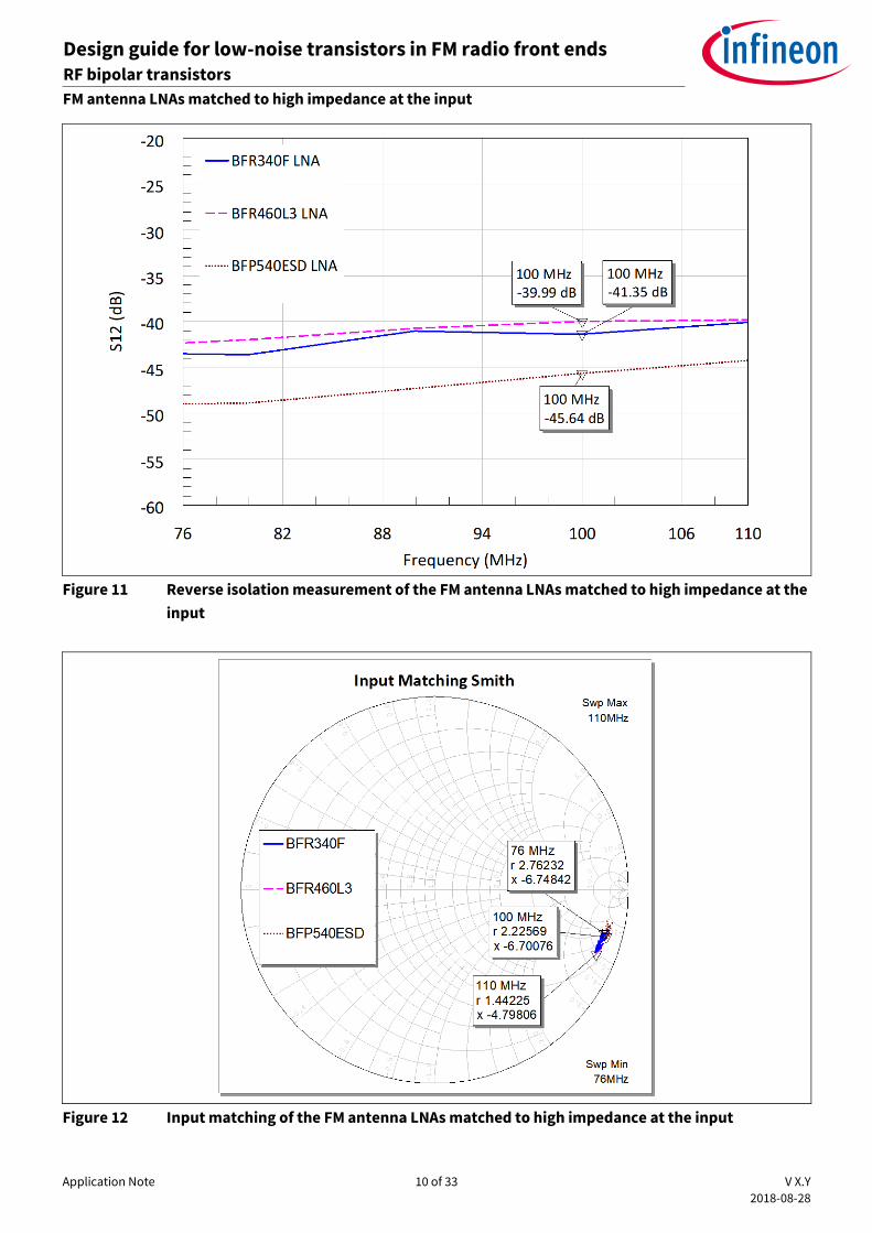
Figure 45 Stability K-factor plots of the FM antenna LNA with low-noise MMIC BGB707L7ESD

Application Note 31 of 33 V X.Y
2018-08-28
Design guide for low-noise transistors in FM radio front ends RF bipolar transistors
Authors
5 Authors
Mamun Md Abdullah Al, RF application engineer of business unit RF and sensors.
Dr. Jie Fang, RF staff application engineer of business unit RF and sensors.

Application Note 32 of 33 V X.Y
2018-08-28
Design guide for low-noise transistors in FM radio front ends RF bipolar transistors
Revision history
Revision history
Document
version
Date of release Description of changes

Trademarks All referenced product or service names and trademarks are the property of their respective owners.
Edition 2018-08-28
AN_1806_PL32_1808_171123
Published by
Infineon Technologies AG
81726 Munich, Germany
© 2018 Infineon Technologies AG.
All Rights Reserved.
Do you have a question about this
document?
Email: [email protected]
Document reference
IMPORTANT NOTICE The information contained in this application note is given as a hint for the implementation of the product only and shall in no event be regarded as a description or warranty of a certain functionality, condition or quality of the product. Before implementation of the product, the recipient of this application note must verify any function and other technical information given herein in the real application. Infineon Technologies hereby disclaims any and all warranties and liabilities of any kind (including without limitation warranties of non-infringement of intellectual property rights of any third party) with respect to any and all information given in this application note. The data contained in this document is exclusively intended for technically trained staff. It is the responsibility of customer’s technical departments to evaluate the suitability of the product for the intended application and the completeness of the product information given in this document with respect to such application.
For further information on the product, technology, delivery terms and conditions and prices please contact your nearest Infineon Technologies office (www.infineon.com).
WARNINGS Due to technical requirements products may contain dangerous substances. For information on the types in question please contact your nearest Infineon Technologies office. Except as otherwise explicitly approved by Infineon Technologies in a written document signed by authorized representatives of Infineon Technologies, Infineon Technologies’ products may not be used in any applications where a failure of the product or any consequences of the use thereof can reasonably be expected to result in personal injury.

![[Chapter III] Basic Knowledge of Discrete Semiconductor ......transistors (IGBTs) Power transistors (2SAxx,2SBxx,2SCxx,2SDxx, TTAxx,TTBxx,TTCxx,TTDxx) Types of Transistors Transistors](https://img.pdfslide.us/doc/110x75/5e766014341a1a707d5f4c34/chapter-iii-basic-knowledge-of-discrete-semiconductor-transistors-igbts.jpg)