Embed Size (px)
Citation preview

Version 2012
Design for Real-Life
ManufacturingMarch 22, 2012
YOUR EMS PARTNER
2
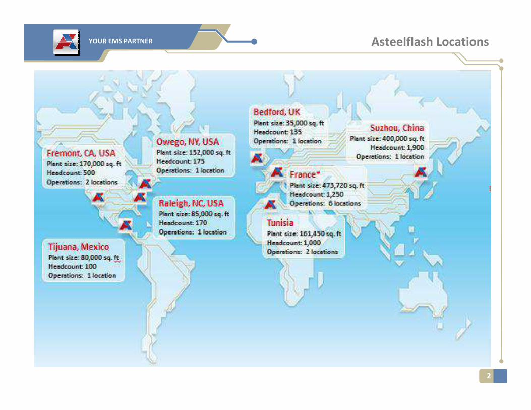
Asteelflash Locations
YOUR EMS PARTNER
3
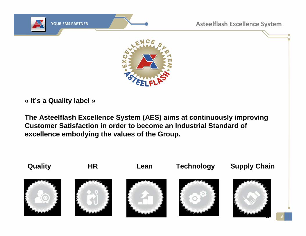
Asteelflash Excellence System
3
Quality HR Lea n Technology Supply Chain
« It’s a Quality label »
The Asteelflash Excellence System (AES) aims at con tinuously improving Customer Satisfaction in order to become an Industr ial Standard of excellence embodying the values of the Group.
YOUR EMS PARTNER
4
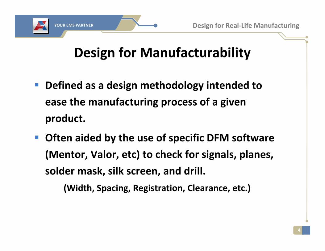
Design for Manufacturability
� Defined as a design methodology intended to
ease the manufacturing process of a given
product.
� Often aided by the use of specific DFM software
(Mentor, Valor, etc) to check for signals, planes,
solder mask, silk screen, and drill.
(Width, Spacing, Registration, Clearance, etc.)
Design for Real-Life Manufacturing
YOUR EMS PARTNER Design for Real-Life Manufacturing
5
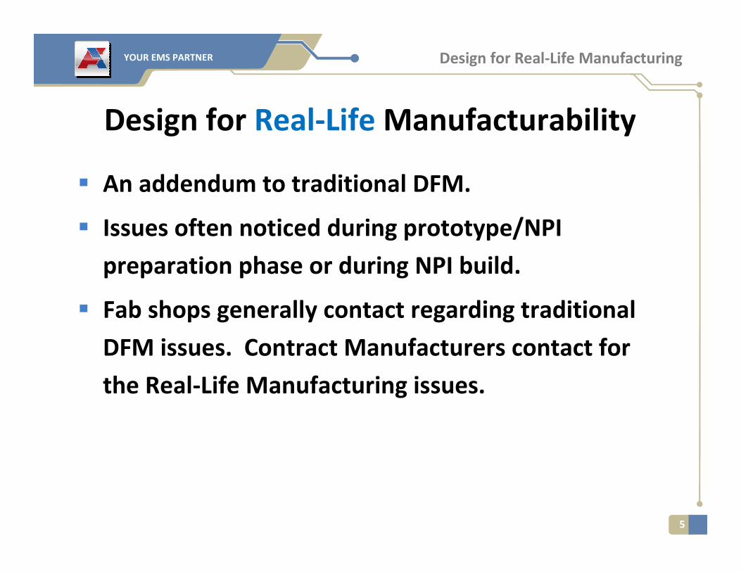
Design for Real-Life Manufacturability
� An addendum to traditional DFM.
� Issues often noticed during prototype/NPI
preparation phase or during NPI build.
� Fab shops generally contact regarding traditional
DFM issues. Contract Manufacturers contact for
the Real-Life Manufacturing issues.
YOUR EMS PARTNER
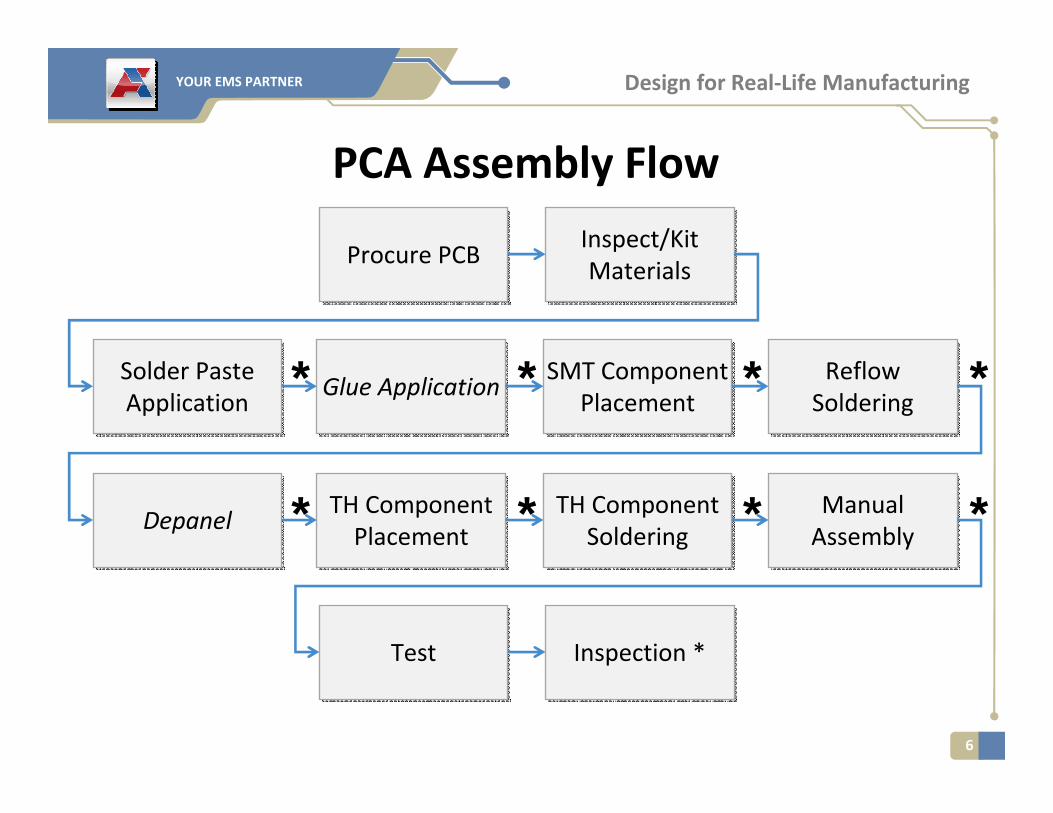
6
Procure PCBProcure PCBInspect/Kit
Materials
Inspect/Kit
Materials
Solder Paste
Application
Solder Paste
ApplicationGlue ApplicationGlue Application
SMT Component
Placement
SMT Component
PlacementReflow
Soldering
Reflow
Soldering
DepanelDepanelTH Component
Placement
TH Component
PlacementTH Component
Soldering
TH Component
SolderingManual
Assembly
Manual
Assembly
TestTest
PCA Assembly Flow
Design for Real-Life Manufacturing
Inspection *Inspection *
* ** *
* ** *
YOUR EMS PARTNER Design for Real-Life Manufacturing
7
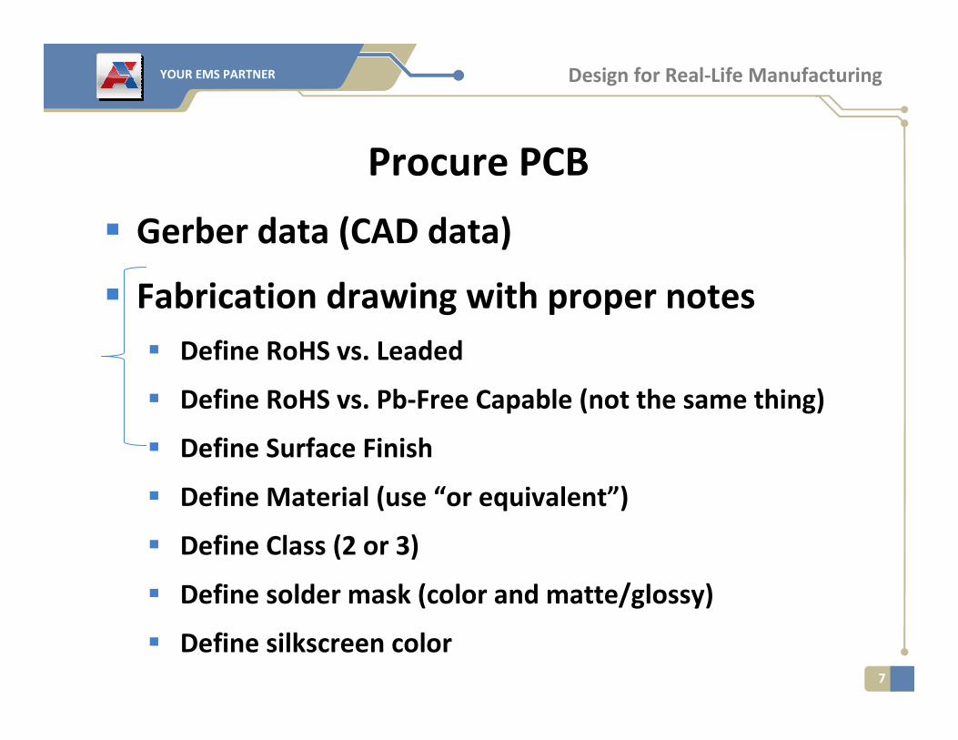
Procure PCB
� Gerber data (CAD data)
� Fabrication drawing with proper notes
� Define RoHS vs. Leaded
� Define RoHS vs. Pb-Free Capable (not the same thing)
� Define Surface Finish
� Define Material (use “or equivalent”)
� Define Class (2 or 3)
� Define solder mask (color and matte/glossy)
� Define silkscreen color
YOUR EMS PARTNER Design for Real-Life Manufacturing
8
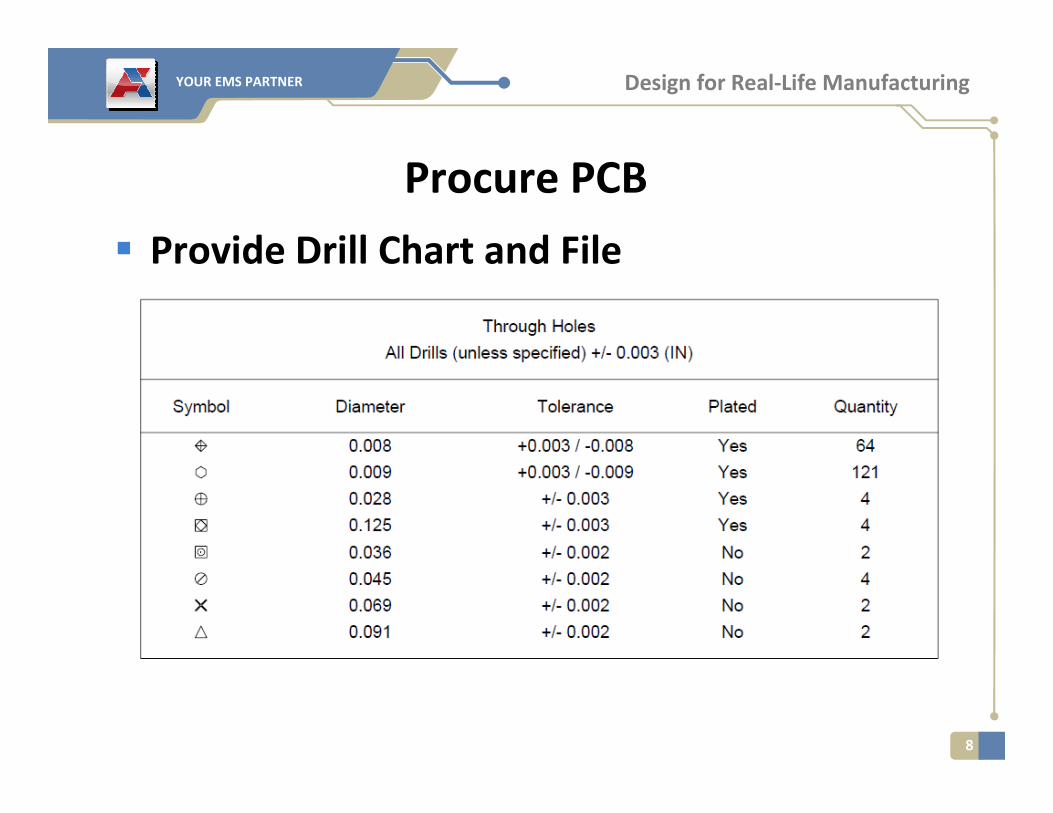
Procure PCB
� Provide Drill Chart and File
YOUR EMS PARTNER Design for Real-Life Manufacturing
9
� Provide Dimensions
� Provide Netlist (IPC File)
� Do NOT provide array/side rails unless
absolutely necessary
Procure PCB
YOUR EMS PARTNER
10
� If the customer/designer decides to procure
the PCB, it is advised to discuss
manufacturing needs with contract
manufacturer before fabrication of board.
Procure PCB
Design for Real-Life Manufacturing
YOUR EMS PARTNER Design for Real-Life Manufacturing
11
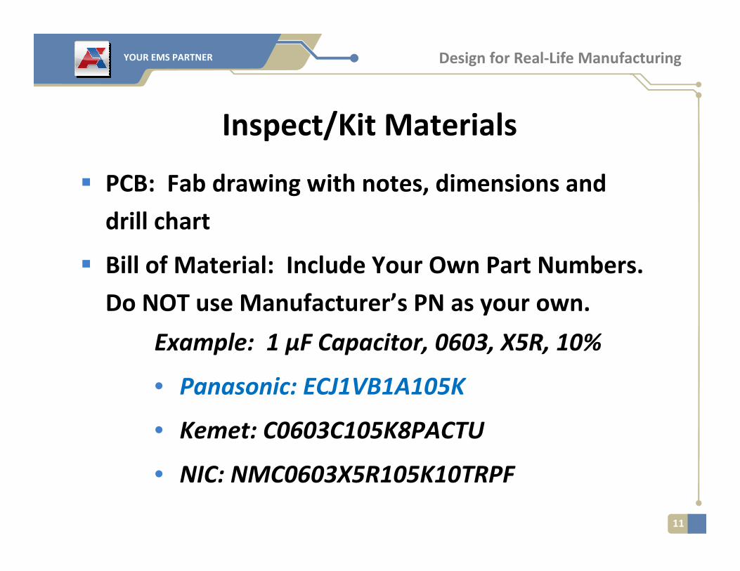
Inspect/Kit Materials
� PCB: Fab drawing with notes, dimensions and
drill chart
� Bill of Material: Include Your Own Part Numbers.
Do NOT use Manufacturer’s PN as your own.
Example: 1 µF Capacitor, 0603, X5R, 10%
• Panasonic: ECJ1VB1A105K
• Kemet: C0603C105K8PACTU
• NIC: NMC0603X5R105K10TRPF
YOUR EMS PARTNER Design for Real-Life Manufacturing
12
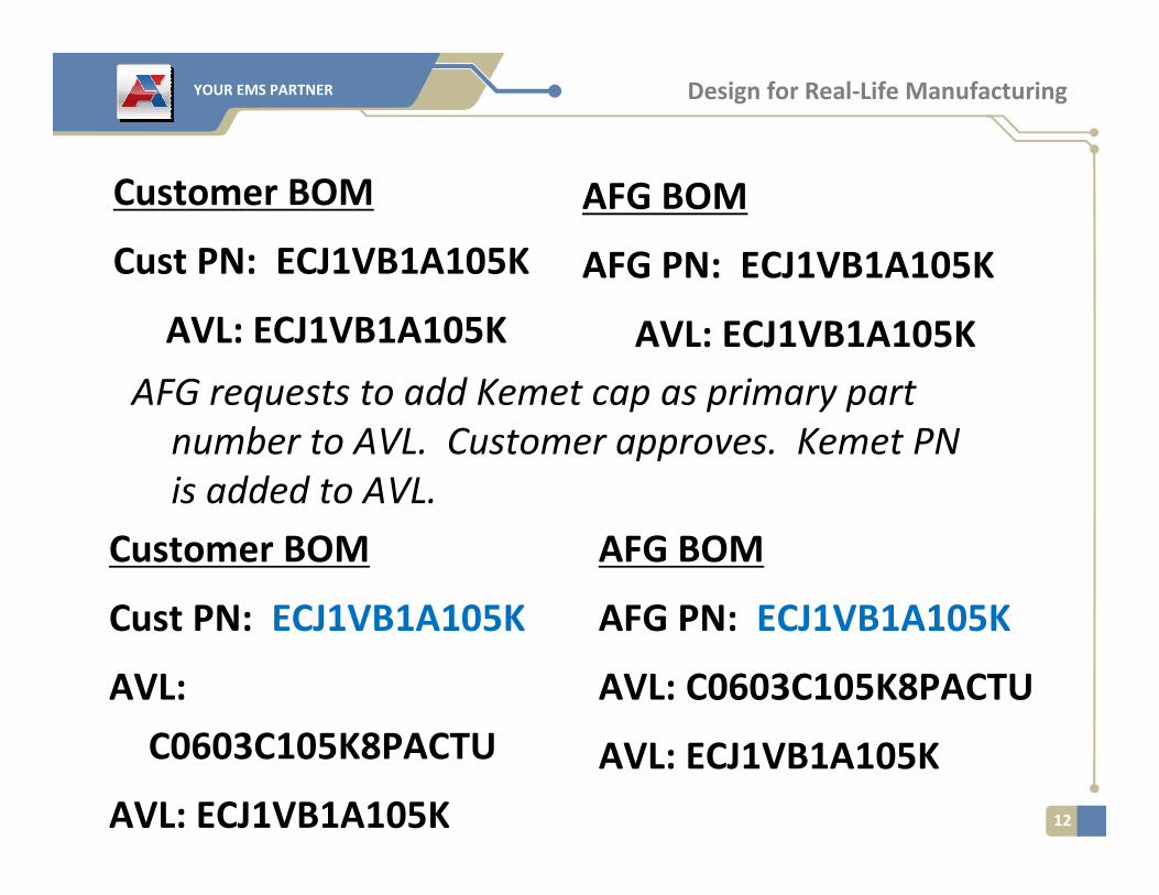
Customer BOM
Cust PN: ECJ1VB1A105K
AVL: ECJ1VB1A105K
AFG BOM
AFG PN: ECJ1VB1A105K
AVL: ECJ1VB1A105K
Customer BOM
Cust PN: ECJ1VB1A105K
AVL:
C0603C105K8PACTU
AVL: ECJ1VB1A105K
AFG BOM
AFG PN: ECJ1VB1A105K
AVL: C0603C105K8PACTU
AVL: ECJ1VB1A105K
AFG requests to add Kemet cap as primary part
number to AVL. Customer approves. Kemet PN
is added to AVL.
YOUR EMS PARTNER Design for Real-Life Manufacturing
13
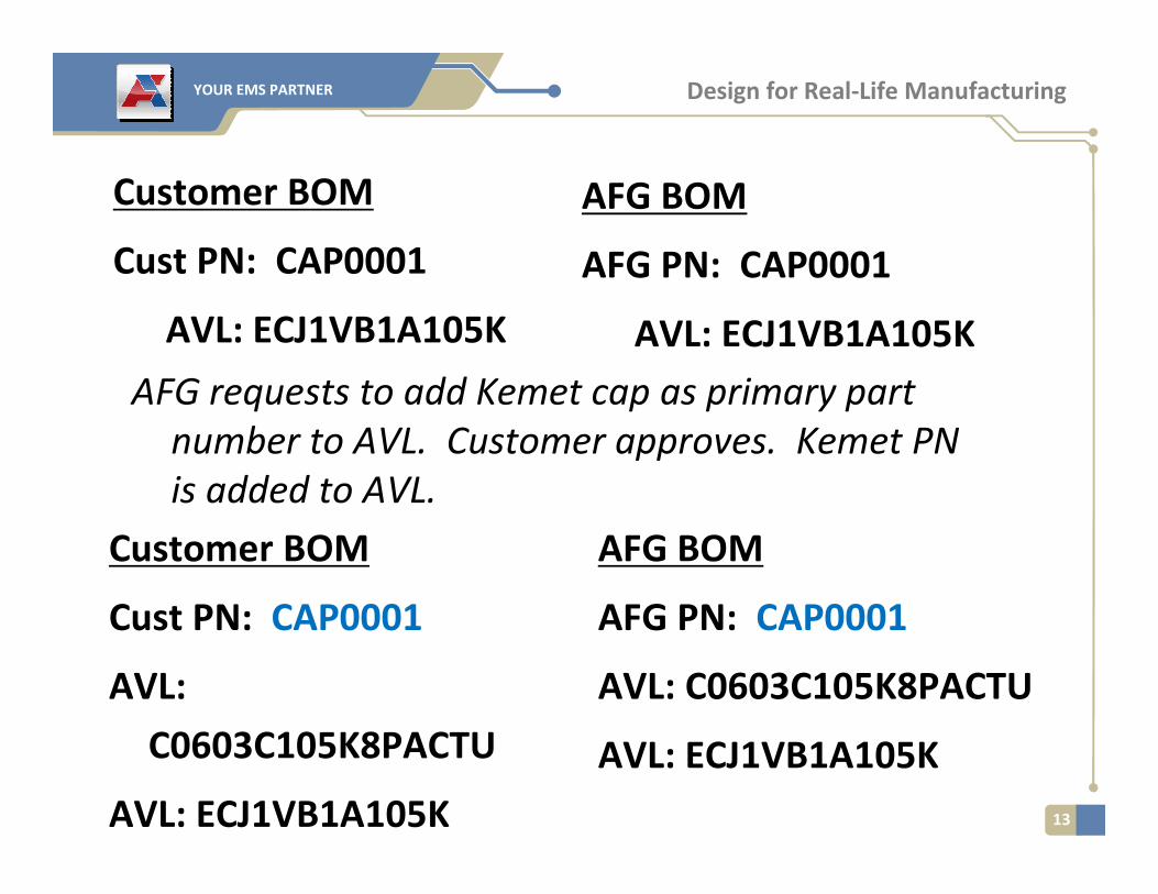
Customer BOM
Cust PN: CAP0001
AVL: ECJ1VB1A105K
AFG BOM
AFG PN: CAP0001
AVL: ECJ1VB1A105K
AFG requests to add Kemet cap as primary part
number to AVL. Customer approves. Kemet PN
is added to AVL.
Customer BOM
Cust PN: CAP0001
AVL:
C0603C105K8PACTU
AVL: ECJ1VB1A105K
AFG BOM
AFG PN: CAP0001
AVL: C0603C105K8PACTU
AVL: ECJ1VB1A105K
YOUR EMS PARTNER Design for Real-Life Manufacturing
14
� Bill of Material: Ensure your part size/type.
� Bill of Material: Understand the packaging (T/R,
strips, tray, bulk).
� AFG prefers reels… this not only speeds the NPI,
but also improves quality. If you want a proto
build fast and with high quality, build it on a
machine!
� Bill of Material: Understand Leaded vs. Pb-Free
vs. RoHS
Inspect/Kit Materials
YOUR EMS PARTNER Design for Real-Life Manufacturing
15
Solder Paste Application
� Documentation Requirements:
� Gerber Data for stencils
� Assembly drawing for paste-type call-out
YOUR EMS PARTNER Design for Real-Life Manufacturing
16
Solder Paste Application
� Considerations:
� Leaded versus Pb-Free
� Global Fiducials
� Pad spacing from board edge
� Paste Layer should equal Artwork Dimensions
� Many CMs have their own stencil design
guidelines or contract design to stencil shop
� Solder Damming between pad and via
YOUR EMS PARTNER Design for Real-Life Manufacturing
17
Blue = ArtworkPink = Provided Paste
Solder Paste ApplicationPaste Layer vs. Artwork
Blue = ArtworkPink = AFG Paste
YOUR EMS PARTNER Design for Real-Life Manufacturing
18
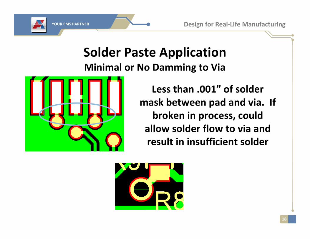
Solder Paste ApplicationMinimal or No Damming to Via
Less than .001” of solder
mask between pad and via. If
broken in process, could
allow solder flow to via and
result in insufficient solder
YOUR EMS PARTNER Design for Real-Life Manufacturing
19
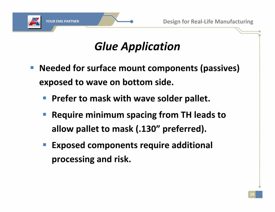
Glue Application
� Needed for surface mount components (passives)
exposed to wave on bottom side.
� Prefer to mask with wave solder pallet.
� Require minimum spacing from TH leads to
allow pallet to mask (.130” preferred).
� Exposed components require additional
processing and risk.
YOUR EMS PARTNER Design for Real-Life Manufacturing
20
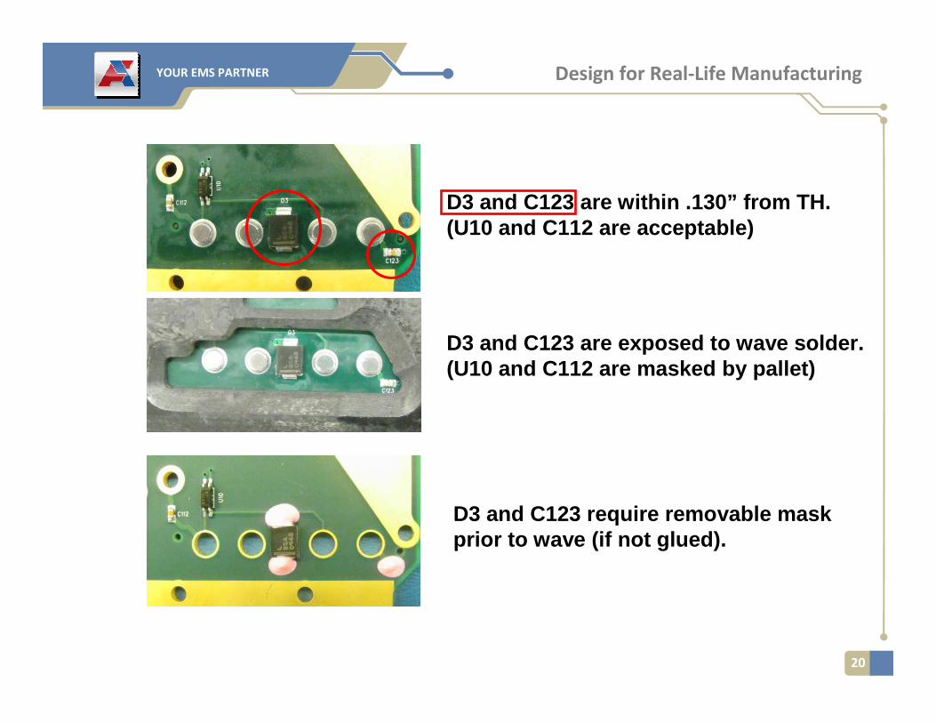
D3 and C123 are within .130” from TH.(U10 and C112 are acceptable)
D3 and C123 are exposed to wave solder.(U10 and C112 are masked by pallet)
D3 and C123 require removable mask prior to wave (if not glued).
YOUR EMS PARTNER Design for Real-Life Manufacturing
21
SMT Placement
� Documentation Required:
� Assembly Drawing
� CAD Data
� Component XY File
� BOM with reference designators
YOUR EMS PARTNER Design for Real-Life Manufacturing
22
SMT Placement
� Placement method (chipshooter, multi, hand)
� Global fiducials required (3 per board...top and
bottom…opposing corners).
� Board/Panel size:
� Minimum width = 3.5” (less requires side rails/array)
� Maximum width/length = 20”
� Optimum size = Letter size paper (8” x 10”)
YOUR EMS PARTNER Design for Real-Life Manufacturing
23
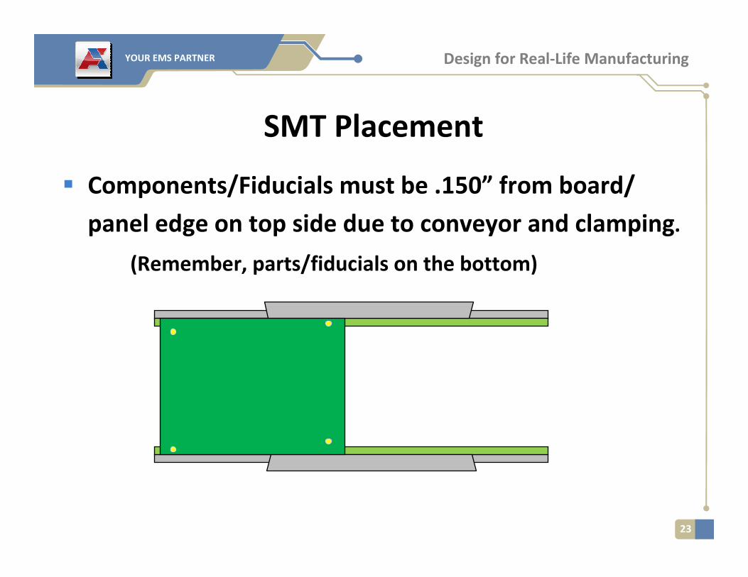
SMT Placement
� Components/Fiducials must be .150” from board/
panel edge on top side due to conveyor and clamping.
(Remember, parts/fiducials on the bottom)
YOUR EMS PARTNER Design for Real-Life Manufacturing
24
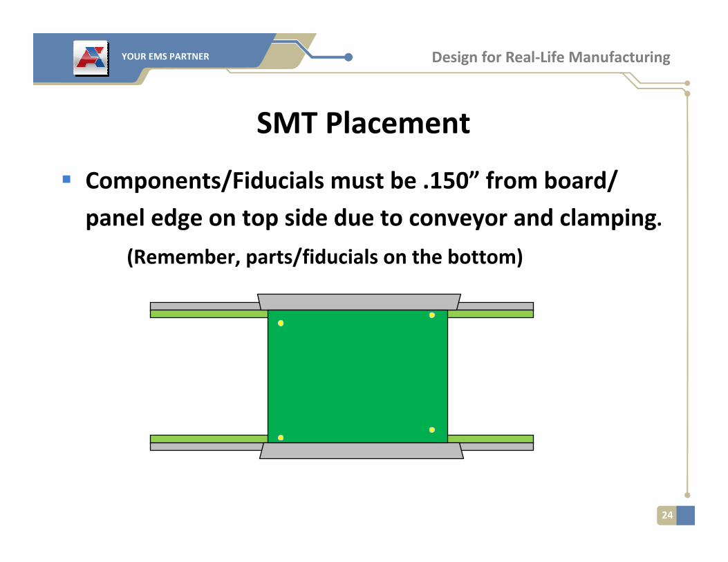
SMT Placement
� Components/Fiducials must be .150” from board/
panel edge on top side due to conveyor and clamping.
(Remember, parts/fiducials on the bottom)
YOUR EMS PARTNER Design for Real-Life Manufacturing
25
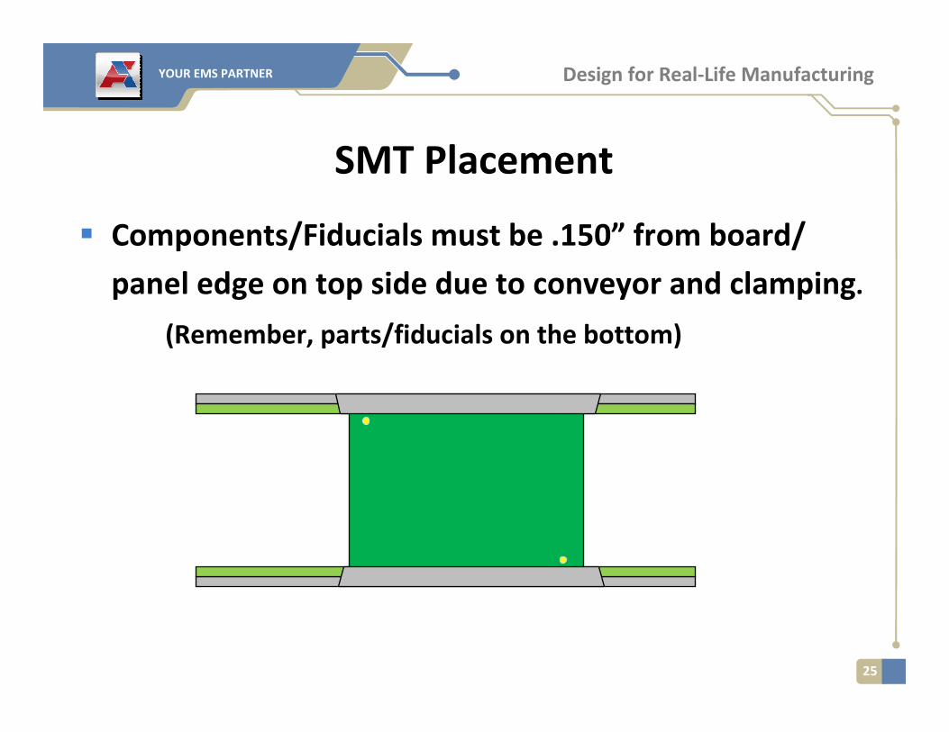
SMT Placement
� Components/Fiducials must be .150” from board/
panel edge on top side due to conveyor and clamping.
(Remember, parts/fiducials on the bottom)
YOUR EMS PARTNER Design for Real-Life Manufacturing
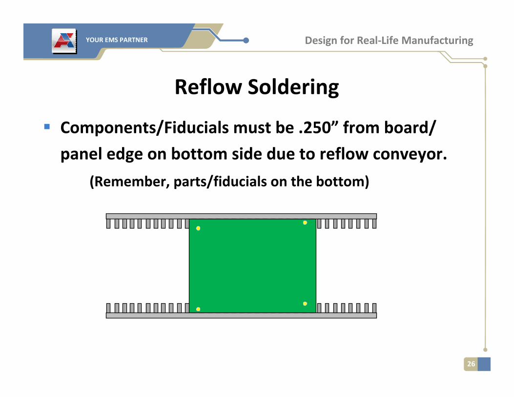
26
Reflow Soldering
� Components/Fiducials must be .250” from board/
panel edge on bottom side due to reflow conveyor.
(Remember, parts/fiducials on the bottom)
YOUR EMS PARTNER Design for Real-Life Manufacturing
27
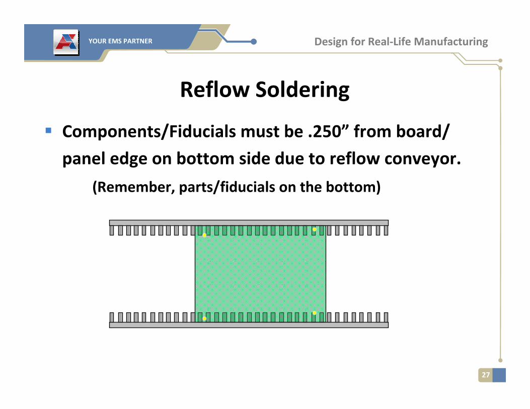
Reflow Soldering
� Components/Fiducials must be .250” from board/
panel edge on bottom side due to reflow conveyor.
(Remember, parts/fiducials on the bottom)
YOUR EMS PARTNER Design for Real-Life Manufacturing
28
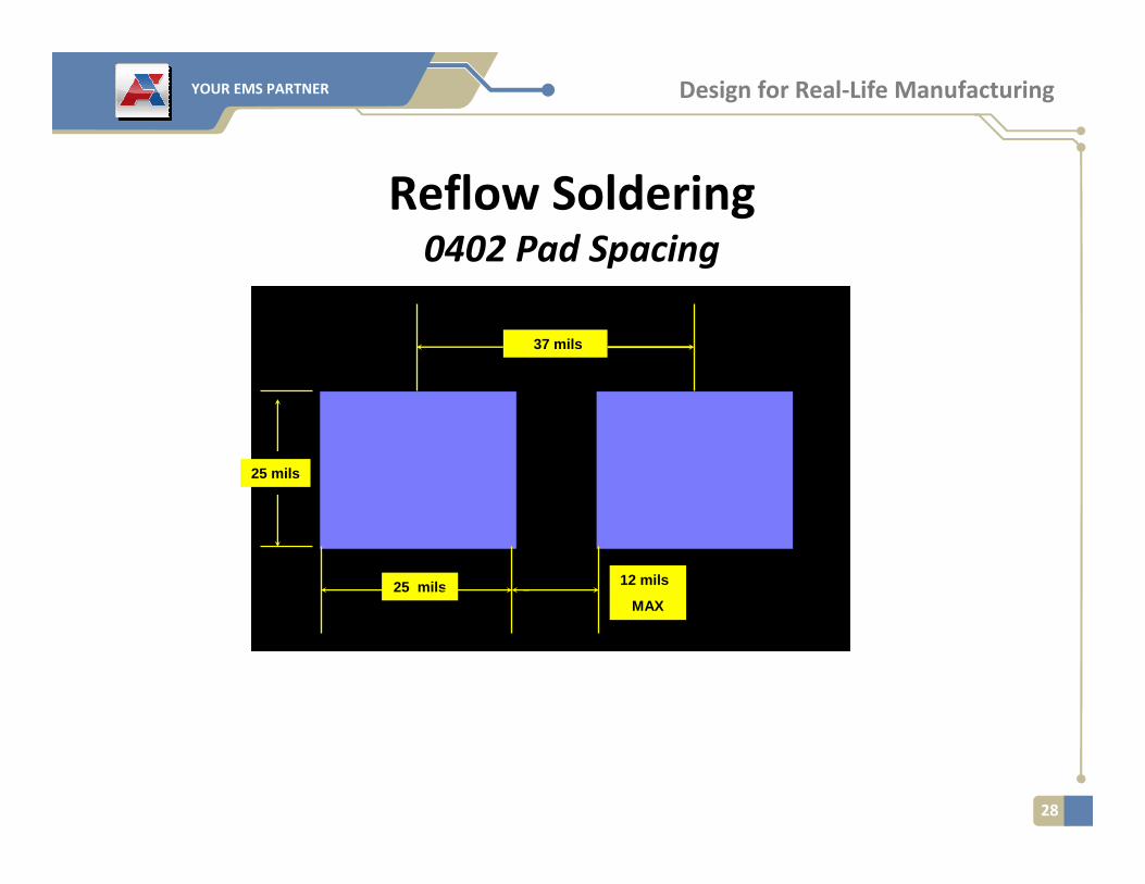
Reflow Soldering0402 Pad Spacing
25 mils
25 mils
37 mils
12 mils
MAX
YOUR EMS PARTNER Design for Real-Life Manufacturing
29
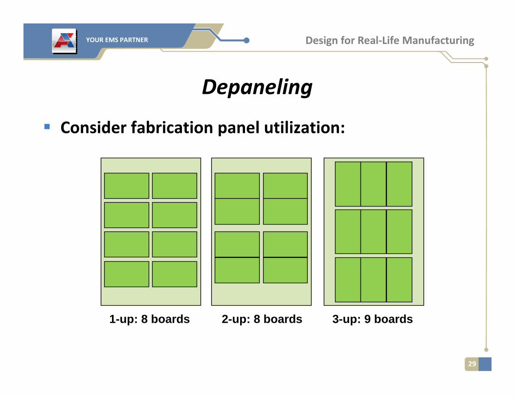
Depaneling
� Consider fabrication panel utilization:
1-up: 8 boards 2-up: 8 boards 3-up: 9 boards
YOUR EMS PARTNER Design for Real-Life Manufacturing
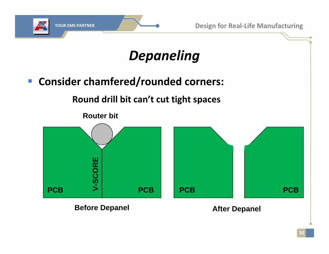
30
Depaneling
� Consider chamfered/rounded corners:
Round drill bit can’t cut tight spaces
Router bit
V-S
CO
RE
Before Depanel After Depanel
PCB PCB PCB PCB
YOUR EMS PARTNER Design for Real-Life Manufacturing
31
Depaneling
� Consider chamfered/rounded corners:
Use double V-SCORE
Router bit
Double V-SCORE
Before DepanelAfter Depanel
PCBPCB PCB PCBScr
ap
Scr
ap
YOUR EMS PARTNER Design for Real-Life Manufacturing
32
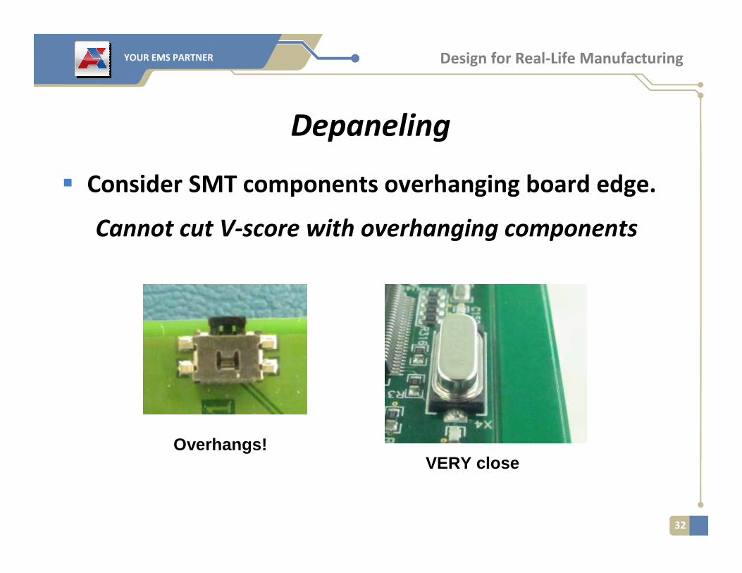
Depaneling
� Consider SMT components overhanging board edge.
Cannot cut V-score with overhanging components
Overhangs!VERY close
YOUR EMS PARTNER Design for Real-Life Manufacturing
33
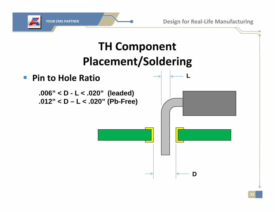
TH Component
Placement/Soldering
� Pin to Hole Ratio L
D
.006” < D - L < .020” (leaded)
.012” < D – L < .020” (Pb-Free)
YOUR EMS PARTNER Design for Real-Life Manufacturing
34
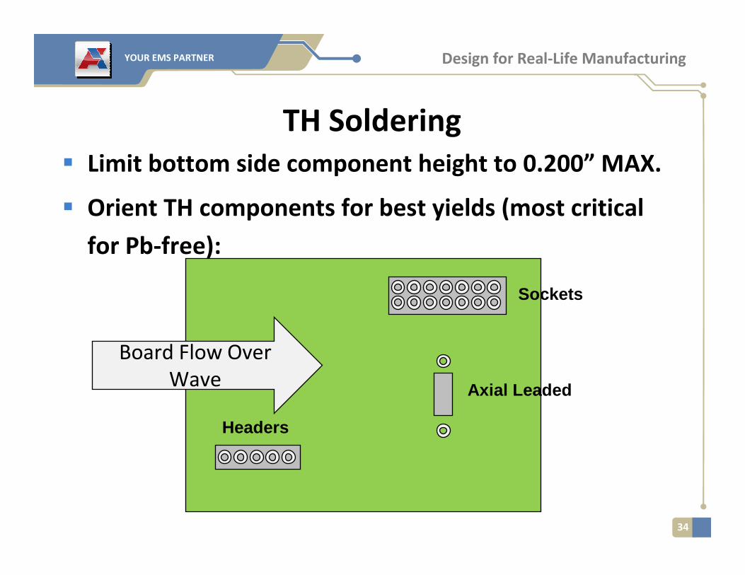
TH Soldering
� Limit bottom side component height to 0.200” MAX.
� Orient TH components for best yields (most critical
for Pb-free):
Axial Leaded
Sockets
Headers
Board Flow Over
Wave
YOUR EMS PARTNER Design for Real-Life Manufacturing
35
Manual Assembly
� Define clearly in Assembly Drawing
Torque, Epoxies, Rev Control, Etc.
� Press-fit connectors vs. solder tail (Press-fit
involves additional tooling charge, but results in
faster process)
� Clearly define labeling
YOUR EMS PARTNER Design for Real-Life Manufacturing
36
Test
� Types: Flying Probe Test, ICT, Functional Test
� Requirements:
� Schematic (PDF Searchable)
� BOM with Reference Designators
� ICT File/Netlist
� Function test procedure/equipment
YOUR EMS PARTNER Design for Real-Life Manufacturing
37
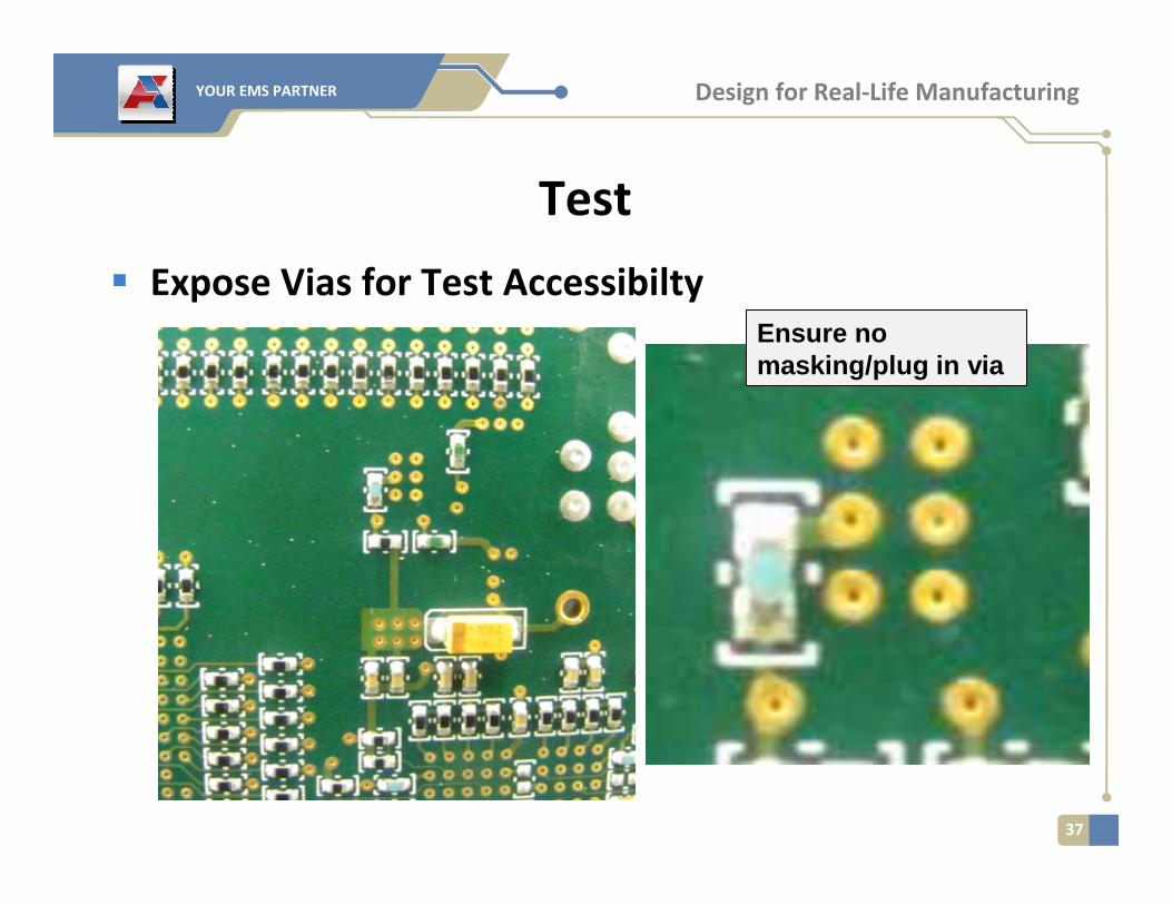
Test
� Expose Vias for Test Accessibilty
Ensure no masking/plug in via
YOUR EMS PARTNER Design for Real-Life Manufacturing
38
InspectionGeneral
� Provide Assembly Drawing with notes and clear
notation regarding orientation and population.
� An assembly drawing in NOT just a silkscreen
layer overlapping a paste/mask layer.
YOUR EMS PARTNER Design for Real-Life Manufacturing
39
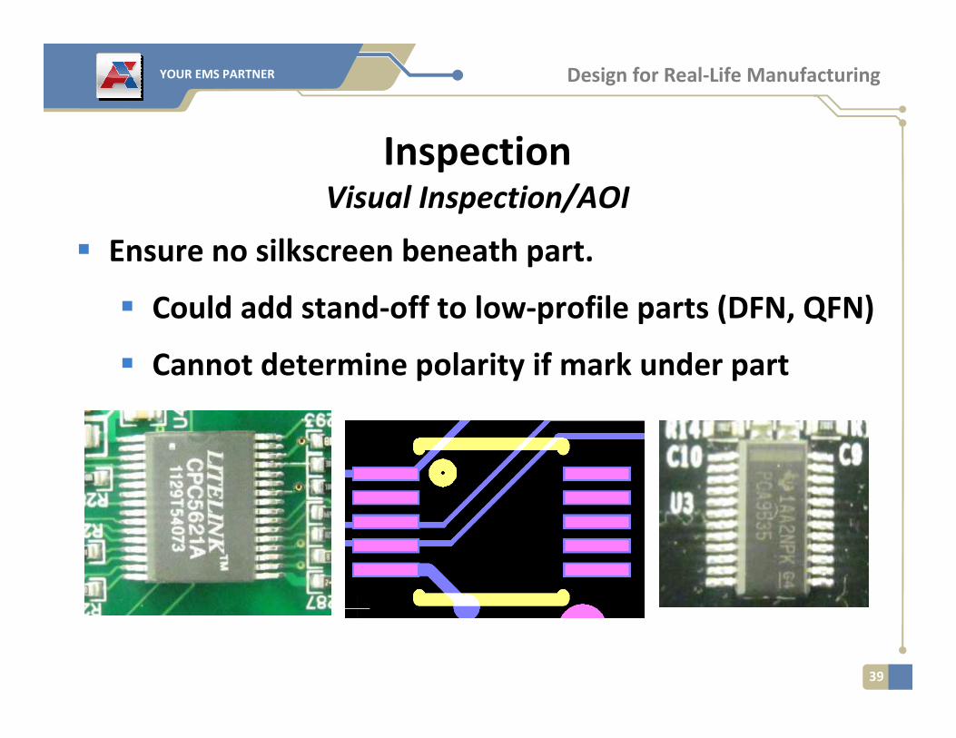
InspectionVisual Inspection/AOI
� Ensure no silkscreen beneath part.
� Could add stand-off to low-profile parts (DFN, QFN)
� Cannot determine polarity if mark under part
YOUR EMS PARTNER Design for Real-Life Manufacturing
40
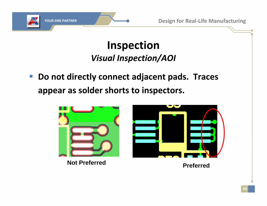
InspectionVisual Inspection/AOI
� Do not directly connect adjacent pads. Traces
appear as solder shorts to inspectors.
Not Preferred Preferred
YOUR EMS PARTNER Design for Real-Life Manufacturing
41
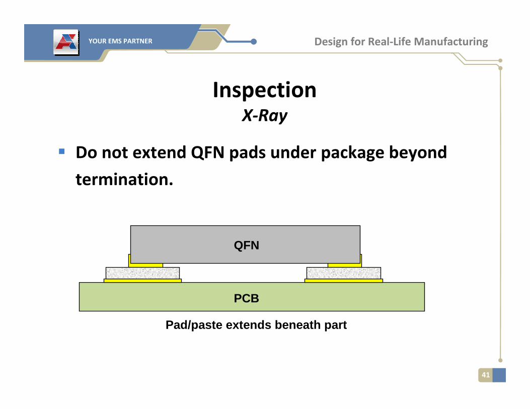
InspectionX-Ray
� Do not extend QFN pads under package beyond
termination.
QFN
PCB
Pad/paste extends beneath part

YOUR EMS PARTNER Design for Real-Life Manufacturing
42
InspectionX-Ray
� Do not extend QFN pads under package beyond
termination.
QFN
PCB
Solder ball forms beneath part
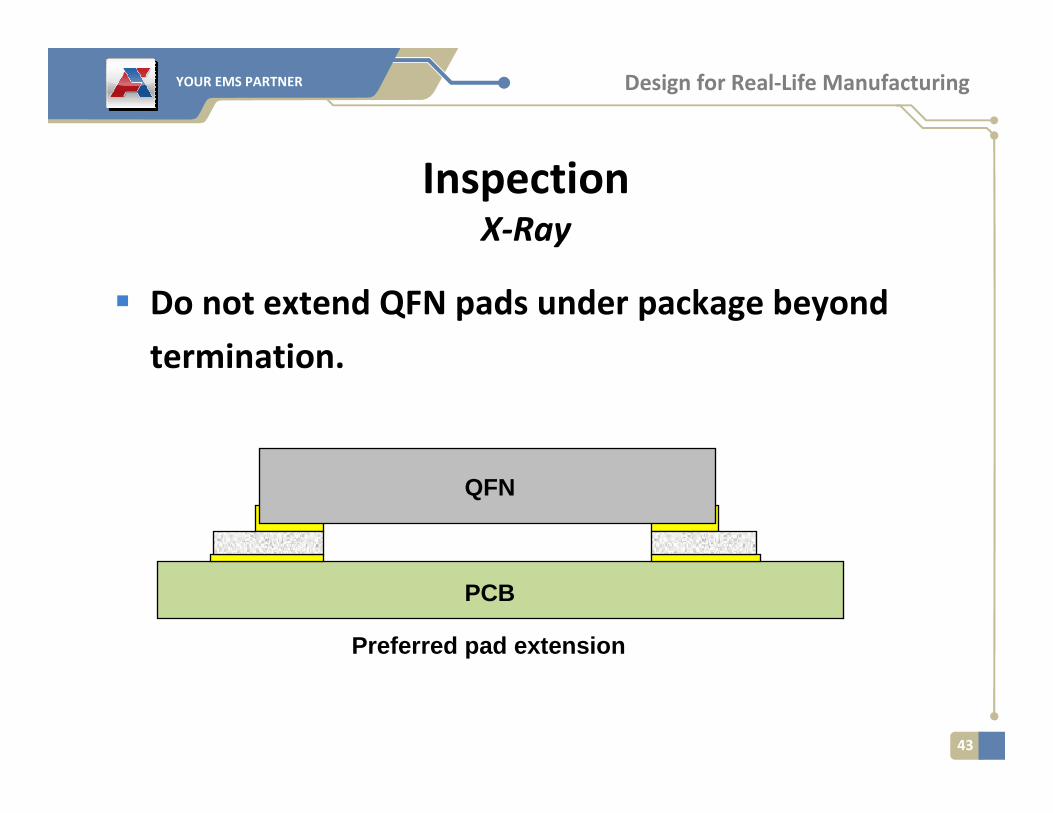
YOUR EMS PARTNER Design for Real-Life Manufacturing
43
InspectionX-Ray
� Do not extend QFN pads under package beyond
termination.
QFN
PCB
Preferred pad extension
YOUR EMS PARTNER Design for Real-Life Manufacturing
44
� Bill of Material with Ref. Des.
� Assembly Drawing with notes
� Fabrication Drawing with notes
� Gerber Data
� CAD Data
Summary:
Required Documentation
YOUR EMS PARTNER Design for Real-Life Manufacturing
45
Required DocumentationBill of Material
� Define unique customer part numbers
� Include AML/AVL (even if single-source)
� Include reference designators
YOUR EMS PARTNER Design for Real-Life Manufacturing
46
Required DocumentationAssembly Drawing
� Define RoHS vs. Leaded
� Define Class (2 vs. 3)
� Define all polarities
� Include proper notes on manual assembly
and labels
� “Not just silkscreen and paste/mask layers”
YOUR EMS PARTNER
47
Design for Real-Life Manufacturing
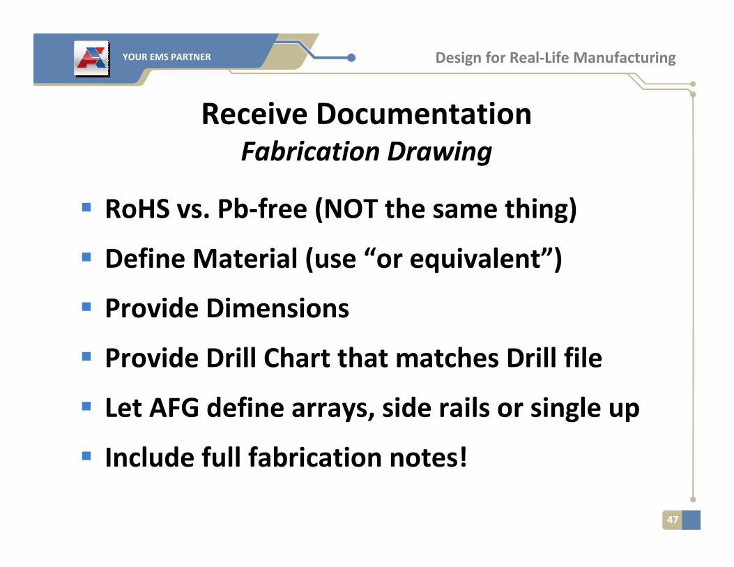
Receive DocumentationFabrication Drawing
� RoHS vs. Pb-free (NOT the same thing)
� Define Material (use “or equivalent”)
� Provide Dimensions
� Provide Drill Chart that matches Drill file
� Let AFG define arrays, side rails or single up
� Include full fabrication notes!
YOUR EMS PARTNER Design for Real-Life Manufacturing
48
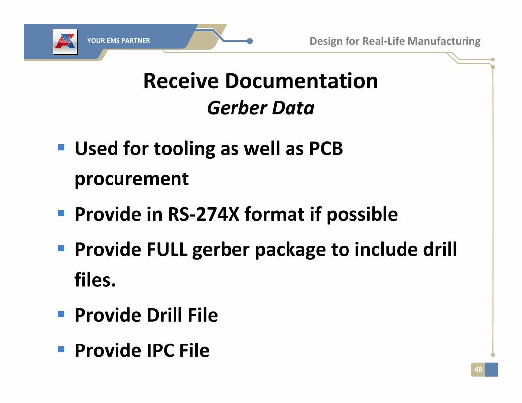
Receive DocumentationGerber Data
� Used for tooling as well as PCB
procurement
� Provide in RS-274X format if possible
� Provide FULL gerber package to include drill
files.
� Provide Drill File
� Provide IPC File
YOUR EMS PARTNER Design for Real-Life Manufacturing
49
Receive DocumentationCAD Data
� Provide full ASCII CAD export.
� Provide Component XY

YOUR EMS PARTNER Design for Real-Life Manufacturing
50
Thank You!
Future Questions please call:
(919) 882-5400