Embed Size (px)
Citation preview

IBM Confidential |© 2007 IBM Corporation
Design Flow
© 2010 IBM CorporationIBM Confidential2
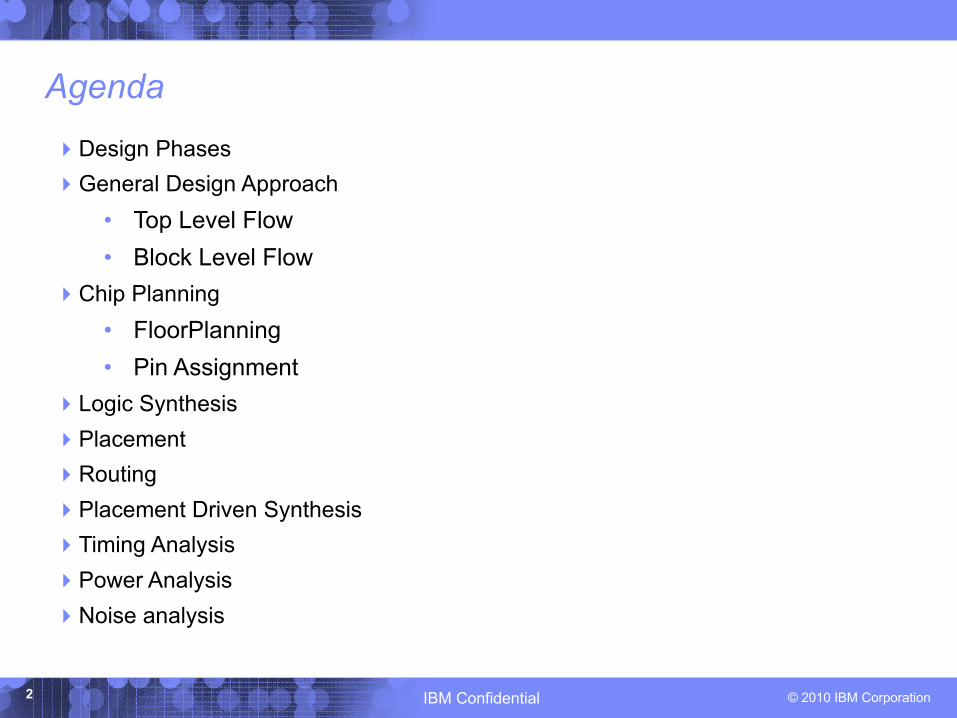
Agenda
4Design Phases4General Design Approach
• Top Level Flow • Block Level Flow
4Chip Planning• FloorPlanning• Pin Assignment
4Logic Synthesis4Placement4Routing4Placement Driven Synthesis4Timing Analysis4Power Analysis4Noise analysis
© 2010 IBM CorporationIBM Confidential3
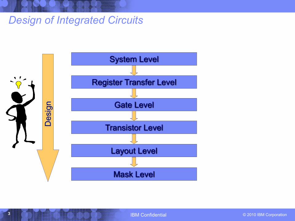
Design of Integrated Circuits
System Level
Register Transfer Level
Gate Level
Transistor Level
Layout Level
Mask Level
© 2010 IBM CorporationIBM Confidential4
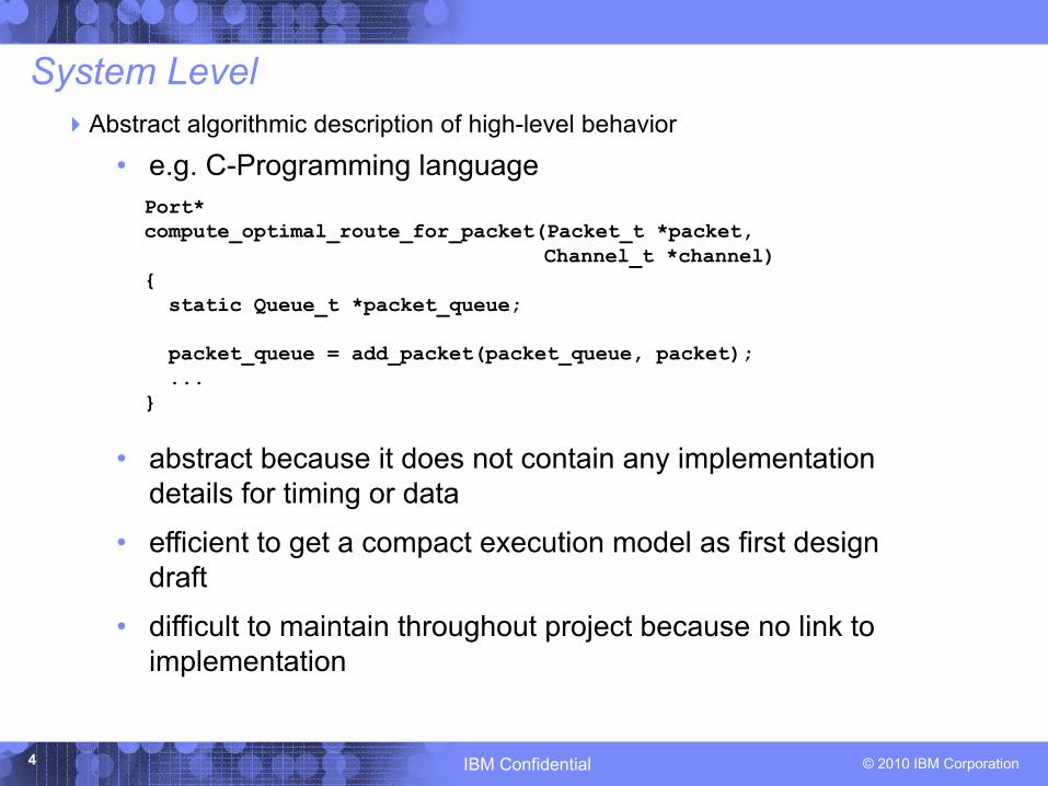
System Level4Abstract algorithmic description of high-level behavior
• e.g. C-Programming language
• abstract because it does not contain any implementation details for timing or data
• efficient to get a compact execution model as first design draft
• difficult to maintain throughout project because no link to implementation
Port*compute_optimal_route_for_packet(Packet_t *packet,
Channel_t *channel){static Queue_t *packet_queue;
packet_queue = add_packet(packet_queue, packet);...
}
© 2010 IBM CorporationIBM Confidential5
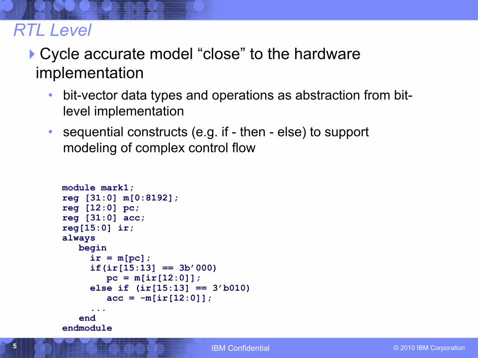
RTL Level4Cycle accurate model “close” to the hardware
implementation• bit-vector data types and operations as abstraction from bit-
level implementation• sequential constructs (e.g. if - then - else) to support
modeling of complex control flow
module mark1;reg [31:0] m[0:8192];reg [12:0] pc;reg [31:0] acc;reg[15:0] ir;always
beginir = m[pc];if(ir[15:13] == 3b’000)
pc = m[ir[12:0]];else if (ir[15:13] == 3’b010)
acc = -m[ir[12:0]];...
endendmodule
© 2010 IBM CorporationIBM Confidential6
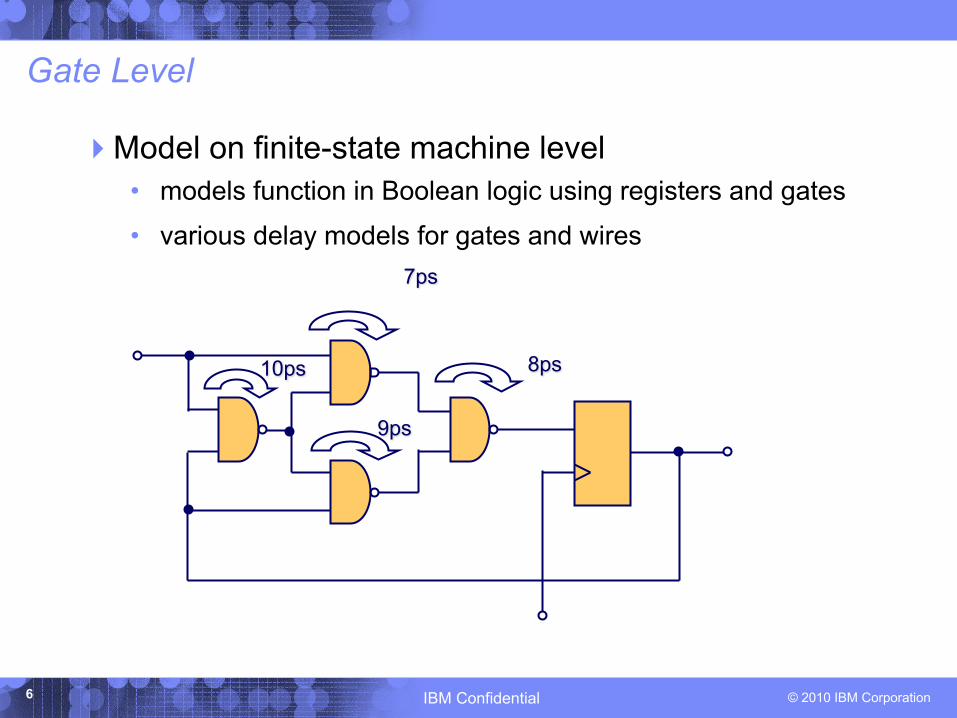
Gate Level
4Model on finite-state machine level• models function in Boolean logic using registers and gates• various delay models for gates and wires
7ps
8ps10ps
9ps
© 2010 IBM CorporationIBM Confidential7
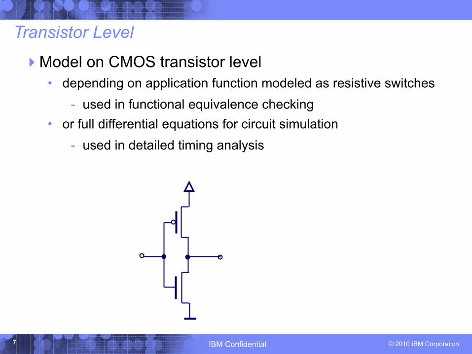
Transistor Level
4Model on CMOS transistor level• depending on application function modeled as resistive switches
- used in functional equivalence checking• or full differential equations for circuit simulation
- used in detailed timing analysis
© 2010 IBM CorporationIBM Confidential8
Layout Level
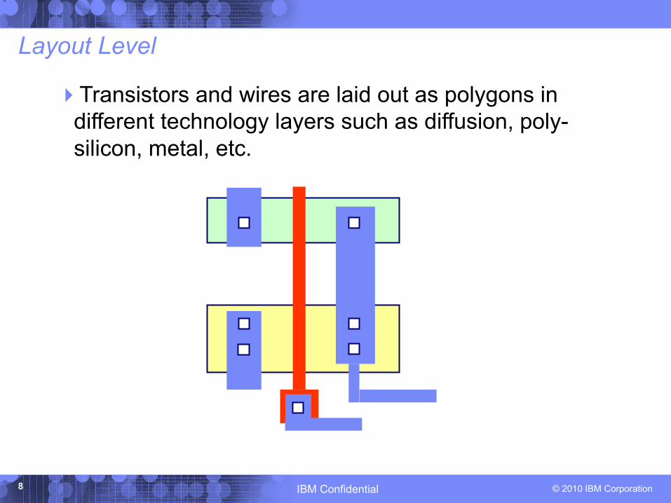
4Transistors and wires are laid out as polygons in different technology layers such as diffusion, poly-silicon, metal, etc.
© 2010 IBM CorporationIBM Confidential9
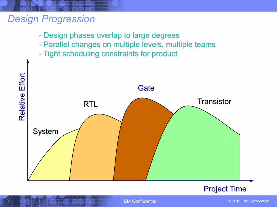
Design ProgressionR
elat
ive
Effo
rt
Project Time
System
RTL
Gate
- Design phases overlap to large degrees- Parallel changes on multiple levels, multiple teams- Tight scheduling constraints for product
Transistor

© 2010 IBM CorporationIBM Confidential10
Design Challenges4Systems are becoming huge, design schedules are getting
tighter• > 2 billion transistors for high end processors• > Half Million lines of C-code to describe system behavior• > 5-10 Million lines of RTL code• > 50 Million gates becoming common for ASICs
4Design teams are getting very large for big projects• several hundred people spread across the globe• differences in skills• concurrent work on multiple levels• management of design complexity and communication very difficult
4Design tools are becoming more complex but still evolving• typical designer has to run ~50 tools on each component• tools have bugs, interfaces do not line up etc.

© 2010 IBM CorporationIBM Confidential11
Design Challenges
4Decision about design point very difficult• compromise between performance / costs / time-to-market• decision has to be made > 3 years before design finished• design points are increasingly difficult to predict without actually
doing the design• scheduling of product cycles
4Functional verification • simulation still main vehicle for functional verification but
inadequate because of size of design space• results in bugs in released hardware that is very expensive to
recover from (different in software ;-)

© 2010 IBM CorporationIBM Confidential12
General Design Approach4How do engineers build a bridge?4Divide and conquer !!!!
• partition design problem into many sub-problems which are manageable
• define mathematical model for sub-problem and find an algorithmic solution
- beware of model limitations and check them !!!!!!!• implement algorithm in individual design tools, define and
implement general interfaces between the tools• implement checking tools for boundary conditions• concatenate design tools to general design flows which can
be managed• see what doesn’t work and start over
© 2010 IBM CorporationIBM Confidential13
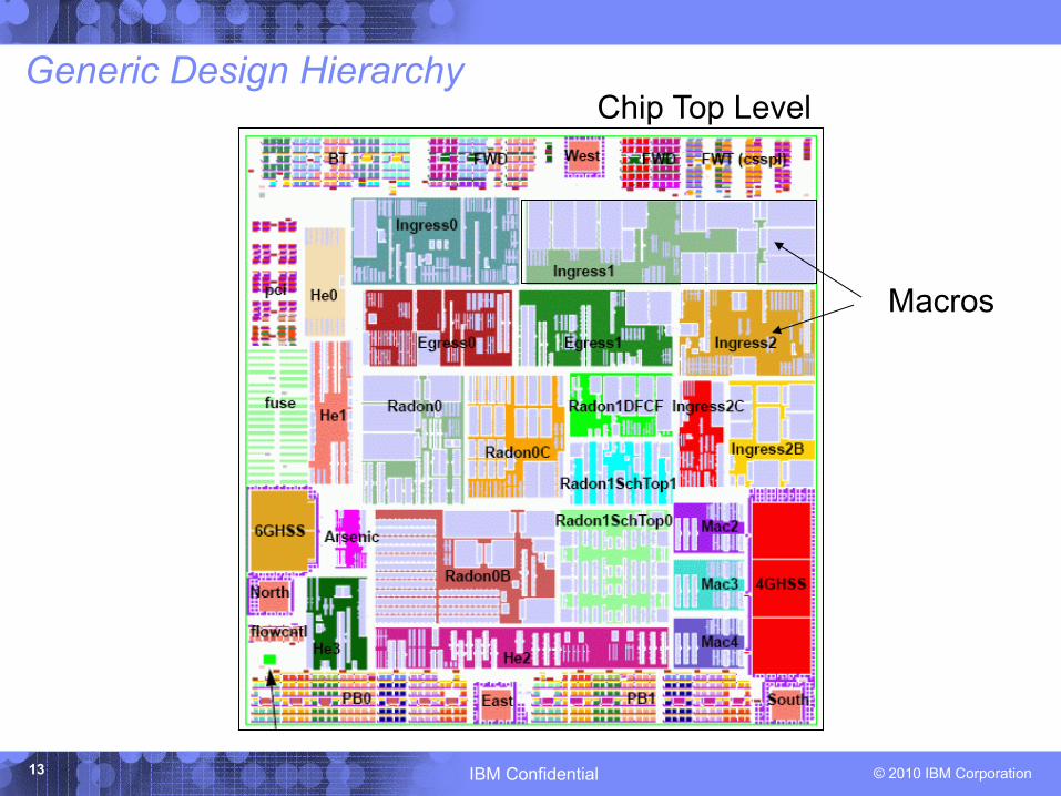
Generic Design HierarchyChip Top Level
Macros
© 2010 IBM CorporationIBM Confidential14
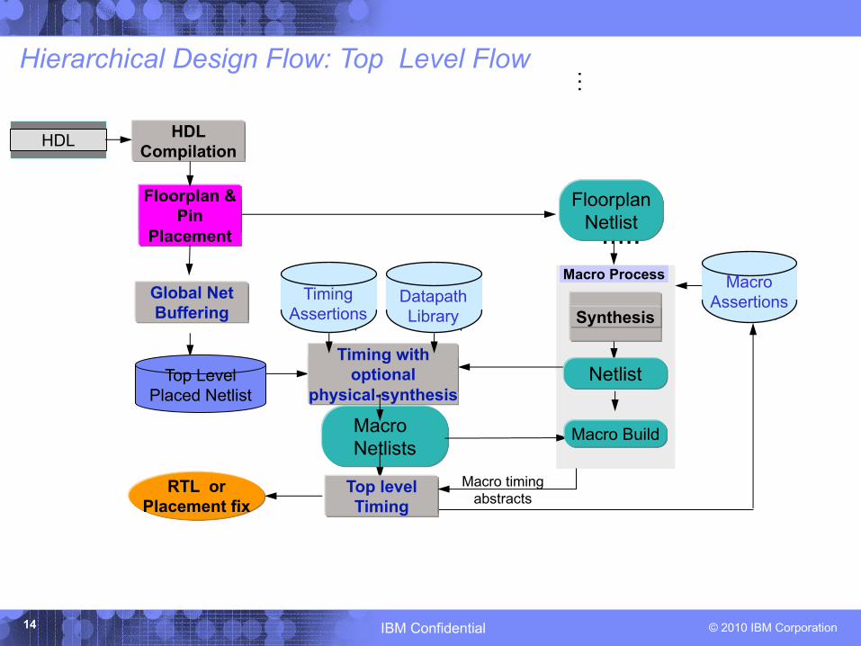
Hierarchical Design Flow: Top Level Flow
.....
...
HDL
RTL or Placement fix
HDL Compilation
Floorplan &Pin
Placement
MacroAssertions
Macro Process
Timing with optional
physical-synthesis
FloorplanNetlist
Synthesis
Netlist
Datapath Library
TimingAssertions
Macro Netlists
Top level Timing
Macro timing abstracts
Global Net Buffering
Top Level Placed Netlist
Macro Build
© 2010 IBM CorporationIBM Confidential15
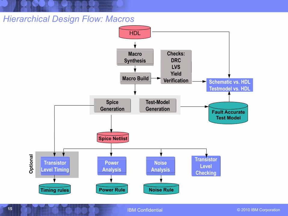
Hierarchical Design Flow: Macros
MacroSynthesis
Macro Build
Checks:DRCLVSYield
Verification
Spice Generation
TransistorLevel Timing
PowerAnalysis
NoiseAnalysis
TransistorLevel
Checking
Test-Model Generation
Schematic vs. HDLTestmodel vs. HDL
HDL
Timing rules Power Rule Noise Rule
Fault Accurate Test Model
Spice Netlist
Opt
iona
l
© 2010 IBM CorporationIBM Confidential16
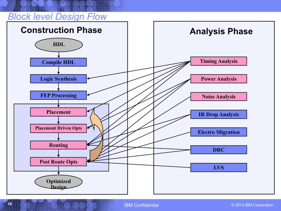
Block level Design Flow
Compile HDL
HDL
Logic Synthesis
FEP Processing
Placement
Placement Driven Opts
Routing
Post Route Opts
Optimized Design
Timing Analysis
Power Analysis
Noise Analysis
IR Drop Analysis
Electro Migration
DRC
LVS
Construction Phase Analysis Phase
© 2010 IBM CorporationIBM Confidential17 17
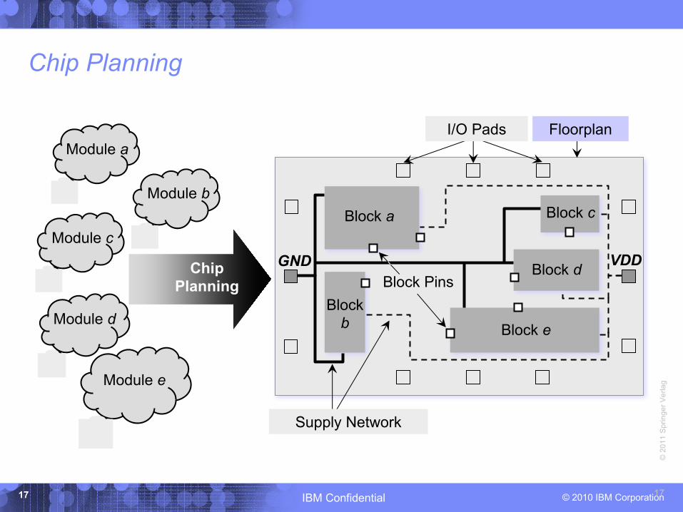
Chip Planning
GND VDD
Module e
I/O Pads
Block Pins
Block a
Blockb
Block d
Block e
Floorplan
Module d
Module c
Module b
Module a
Chip Planning
Block c
Supply Network
© 2
011
Sprin
ger V
erla
g
© 2010 IBM CorporationIBM Confidential18 18
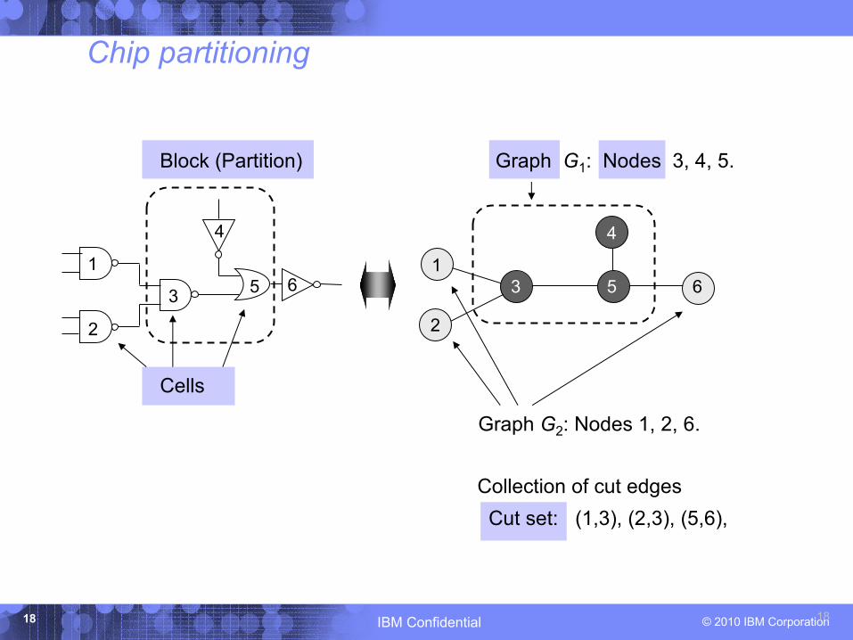
Chip partitioning
5 6
4
2
1
3 3
2
4
5 61
Graph G2: Nodes 1, 2, 6.
Graph G1: Nodes 3, 4, 5.
Collection of cut edges Cut set: (1,3), (2,3), (5,6),
Block (Partition)
Cells
© 2010 IBM CorporationIBM Confidential19 19
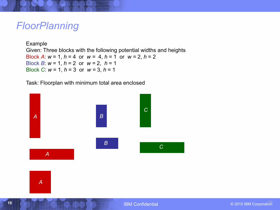
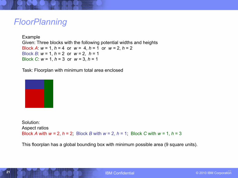
FloorPlanningExampleGiven: Three blocks with the following potential widths and heights Block A: w = 1, h = 4 or w = 4, h = 1 or w = 2, h = 2Block B: w = 1, h = 2 or w = 2, h = 1 Block C: w = 1, h = 3 or w = 3, h = 1
Task: Floorplan with minimum total area enclosed
A
A
A
B
BC
C
© 2010 IBM CorporationIBM Confidential20 20
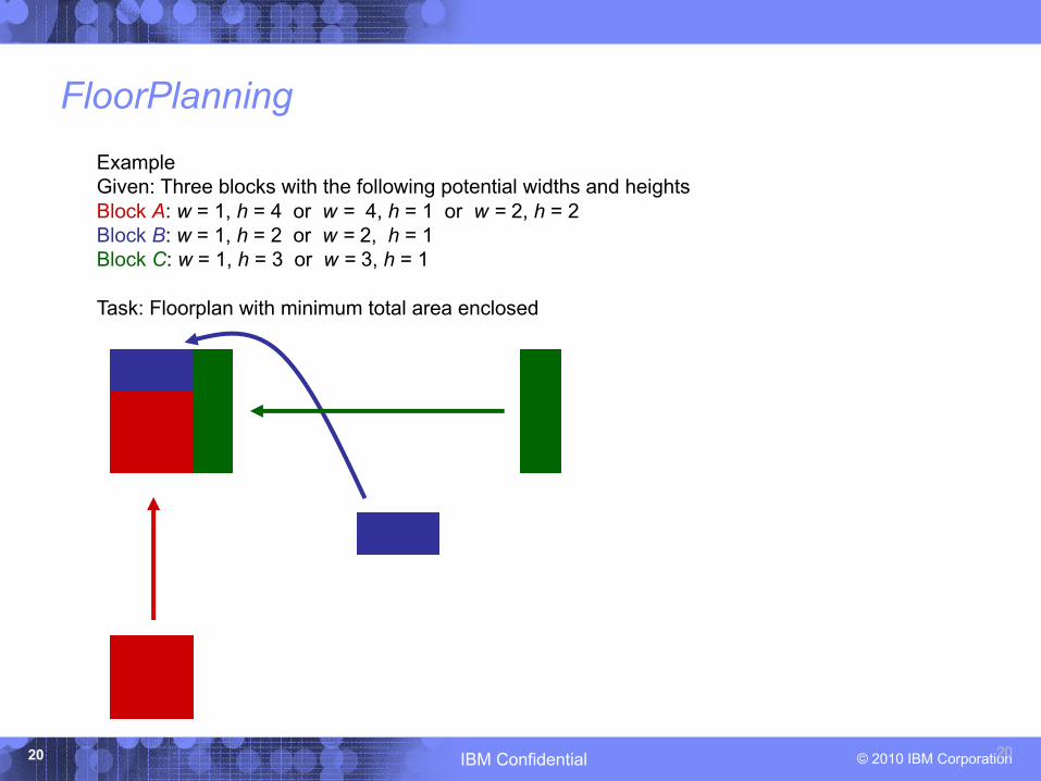
FloorPlanningExampleGiven: Three blocks with the following potential widths and heights Block A: w = 1, h = 4 or w = 4, h = 1 or w = 2, h = 2Block B: w = 1, h = 2 or w = 2, h = 1 Block C: w = 1, h = 3 or w = 3, h = 1
Task: Floorplan with minimum total area enclosed
© 2010 IBM CorporationIBM Confidential21 21
FloorPlanning
Solution:Aspect ratiosBlock A with w = 2, h = 2; Block B with w = 2, h = 1; Block C with w = 1, h = 3
This floorplan has a global bounding box with minimum possible area (9 square units).
ExampleGiven: Three blocks with the following potential widths and heights Block A: w = 1, h = 4 or w = 4, h = 1 or w = 2, h = 2Block B: w = 1, h = 2 or w = 2, h = 1 Block C: w = 1, h = 3 or w = 3, h = 1
Task: Floorplan with minimum total area enclosed
© 2010 IBM CorporationIBM Confidential22 22
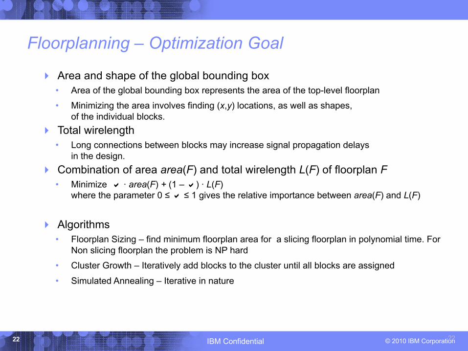
Floorplanning – Optimization Goal
4 Area and shape of the global bounding box• Area of the global bounding box represents the area of the top-level floorplan• Minimizing the area involves finding (x,y) locations, as well as shapes,
of the individual blocks. 4 Total wirelength
• Long connections between blocks may increase signal propagation delays in the design.
4 Combination of area area(F) and total wirelength L(F) of floorplan F• Minimize a ∙ area(F) + (1 – a) ∙ L(F)
where the parameter 0 ≤ a ≤ 1 gives the relative importance between area(F) and L(F)
4 Algorithms• Floorplan Sizing – find minimum floorplan area for a slicing floorplan in polynomial time. For
Non slicing floorplan the problem is NP hard• Cluster Growth – Iteratively add blocks to the cluster until all blocks are assigned• Simulated Annealing – Iterative in nature
© 2010 IBM CorporationIBM Confidential23
Logic Synthesis
4Input: RTL; Output: Gate level optimized netlist4Objective:
• Minimize area- in terms of literal count, cell count, register count, etc.
• Minimize power- in terms of switching activity in individual gates, deactivated circuit
blocks, etc.• Maximize performance
- in terms of maximal clock frequency of synchronous systems, throughput for asynchronous systems
• Any combination of the above- combined with different weights- formulated as a constraint problem
§ “minimize area for a clock speed > 3 GHz”• More global objectives
- feedback from layout: actual physical sizes, delays, placement and routing

© 2010 IBM CorporationIBM Confidential24
Logic Synthesis
4Logic Synthesis Sub-steps…
RTL
… To Timing-Driven Placement
Logic Restructuring
Early Timing Correction
Merge Clock Logic
Technology Mapping
technology-independent
optimizations
© 2010 IBM CorporationIBM Confidential25
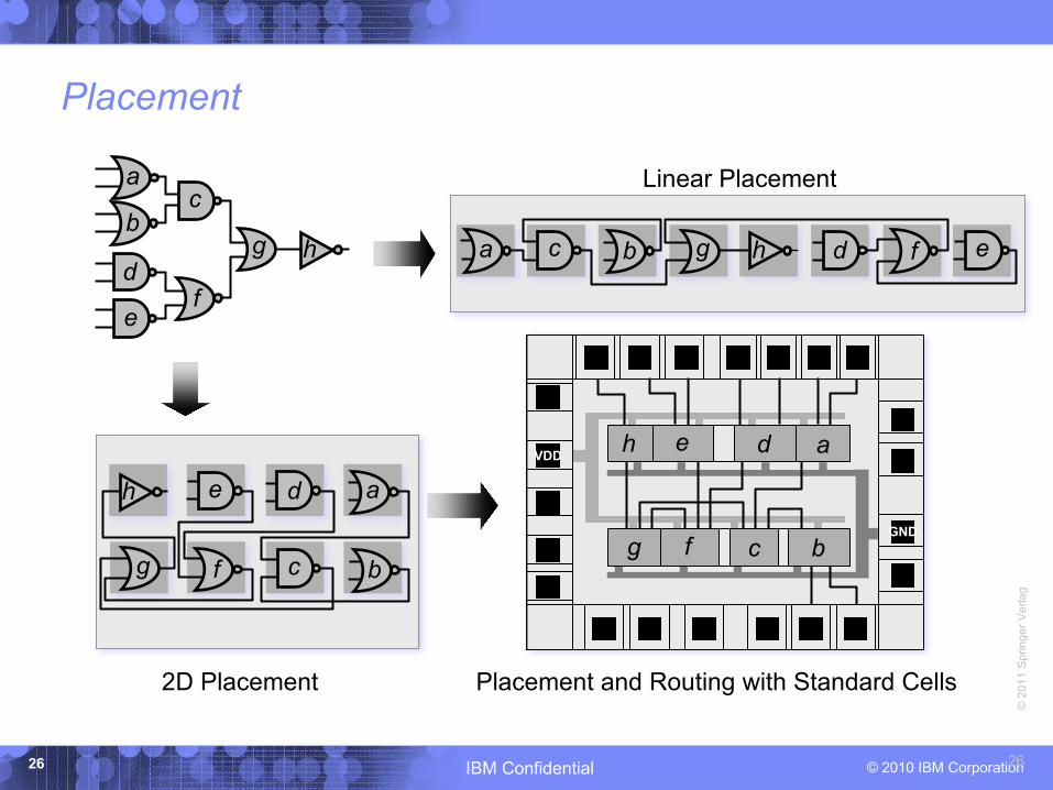
Placement
4 Input• Netlist of connected circuit elements and nets
4 Output• Exact locations of circuit elements without overlaps
4 Goal is to guarantee routability, but extremely difficult to model this
4 Usually use wirelength minimization• S Length(net i)
4 How to estimate length of a net• Half perimeter wire length model (HPWL)• Minimum Spanning Tree (MST)• Steiner Tree (ST)
Courtsey: G.J.Nam, P. Villarrubia
© 2010 IBM CorporationIBM Confidential26 26
Placement
© 2
011
Sprin
ger V
erla
g
c
h
f
b
a
gd
e
a c b hg d ef
eh
g f
d a
c b
GND
VDD
Linear Placement
2D Placement Placement and Routing with Standard Cells
h e d a
g f c b
© 2010 IBM CorporationIBM Confidential27 27
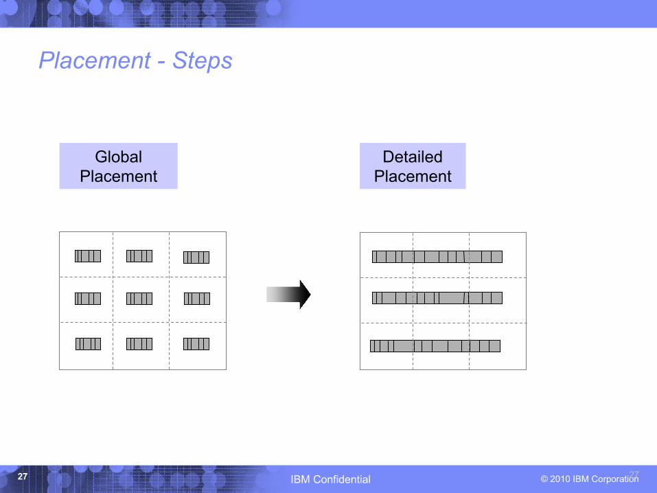
Placement - Steps
Global Placement
Detailed Placement
© 2010 IBM CorporationIBM Confidential28
Routing4Input
• Placed netlist and technology information4Output
• Physically connected cells 4Goal is to
• determine the necessary wiring, e.g., net topologies and specific routing segments, to connect these cells
• while respecting constraints, e.g., design rules and routing resource capacities, and
• optimizing routing objectives, e.g., minimizing total wirelength and maximizing timing slack
Courtsey: A. Huber
© 2010 IBM CorporationIBM Confidential29 29
C
D
A
B
43
214
3
4
1
1
654
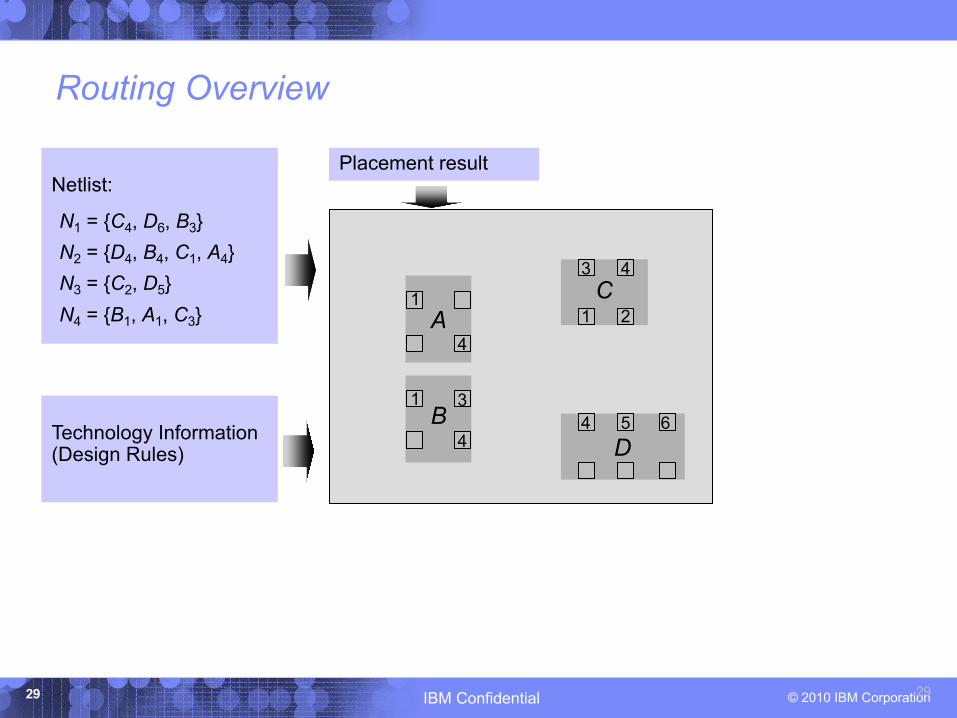
Netlist:
N1 = {C4, D6, B3} N2 = {D4, B4, C1, A4}N3 = {C2, D5}N4 = {B1, A1, C3}
Technology Information (Design Rules)
Placement result
Routing Overview

© 2010 IBM CorporationIBM Confidential30 30
Netlist:
N1 = {C4, D6, B3}N2 = {D4, B4, C1, A4}N3 = {C2, D5}N4 = {B1, A1, C3}
Technology Information (Design Rules)
Routing Overview
C
D
A
B
43
214
3
4
1
1
654
N1
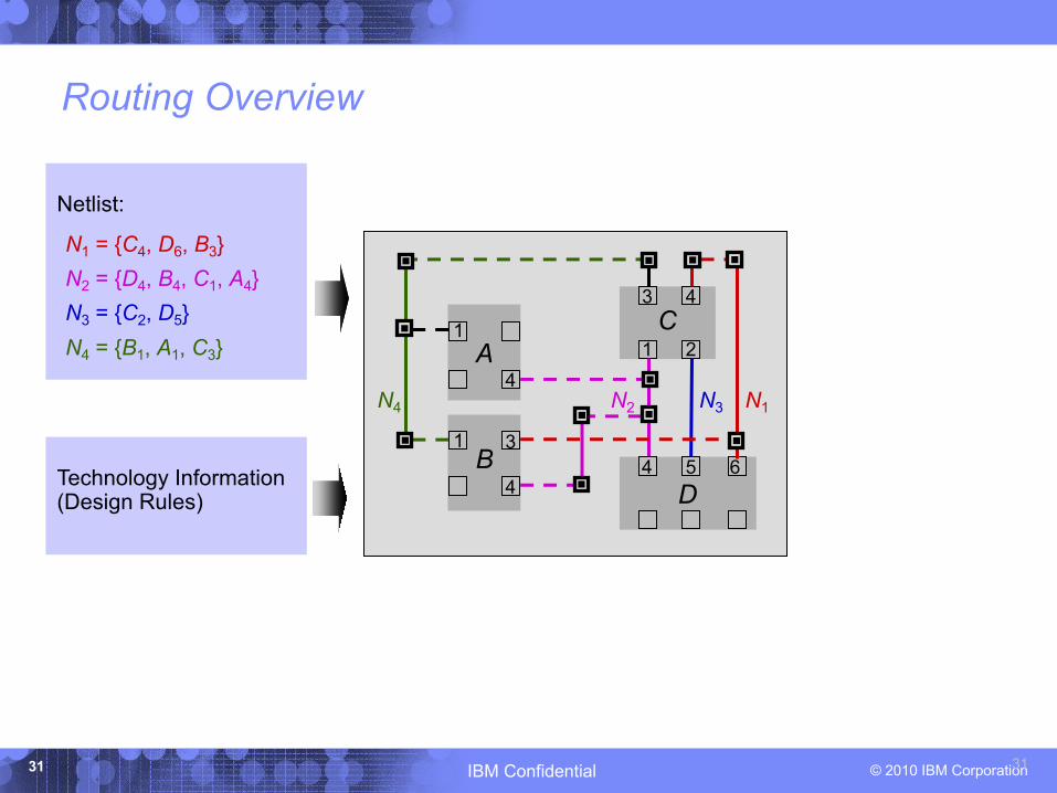
© 2010 IBM CorporationIBM Confidential31 31
Netlist:
N1 = {C4, D6, B3}N2 = {D4, B4, C1, A4}N3 = {C2, D5}N4 = {B1, A1, C3}
Technology Information (Design Rules)
Routing Overview
C
D
A
B
43
214
3
4
1
1
654
N2 N3N4 N1
© 2010 IBM CorporationIBM Confidential32 32
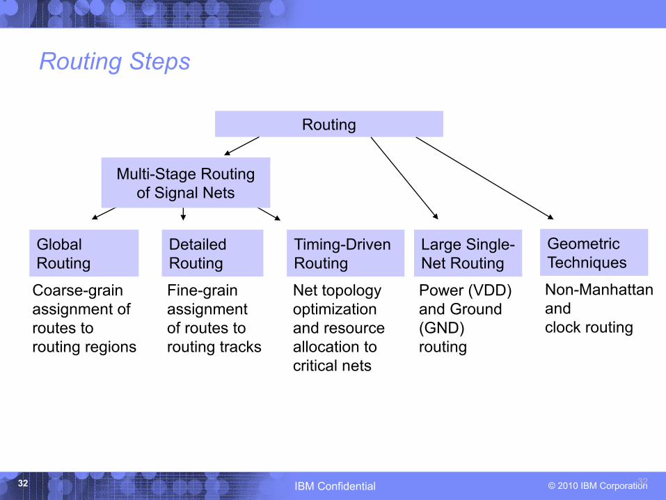
Timing-Driven Routing
GlobalRouting
DetailedRouting
Large Single-Net Routing
Coarse-grain assignment of routes to routing regions
Fine-grain assignment of routes to routing tracks
Net topology optimization and resource allocation to critical nets
Power (VDD) and Ground (GND)routing
Routing
Geometric Techniques
Non-Manhattanand clock routing
Routing Steps
Multi-Stage Routing of Signal Nets
© 2010 IBM CorporationIBM Confidential33
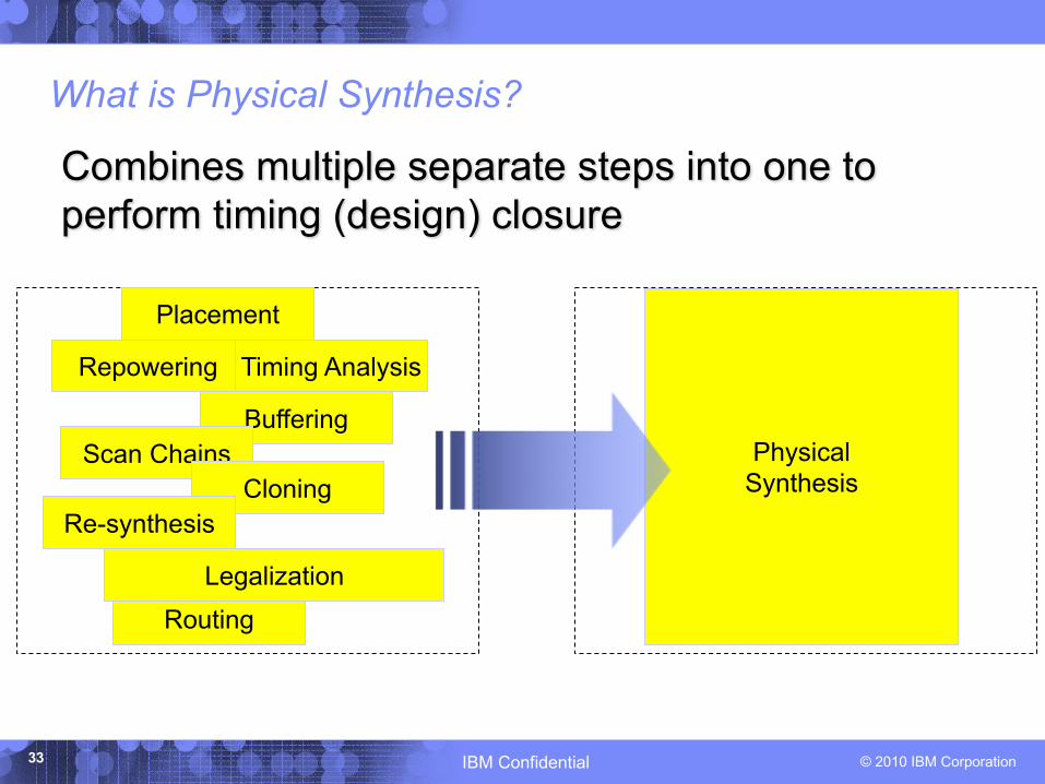
What is Physical Synthesis?
Placement
Buffering
Repowering
Scan ChainsCloning
Routing
Timing Analysis
Legalization
Re-synthesis
PhysicalSynthesis
Combines multiple separate steps into one to perform timing (design) closure
© 2010 IBM CorporationIBM Confidential34
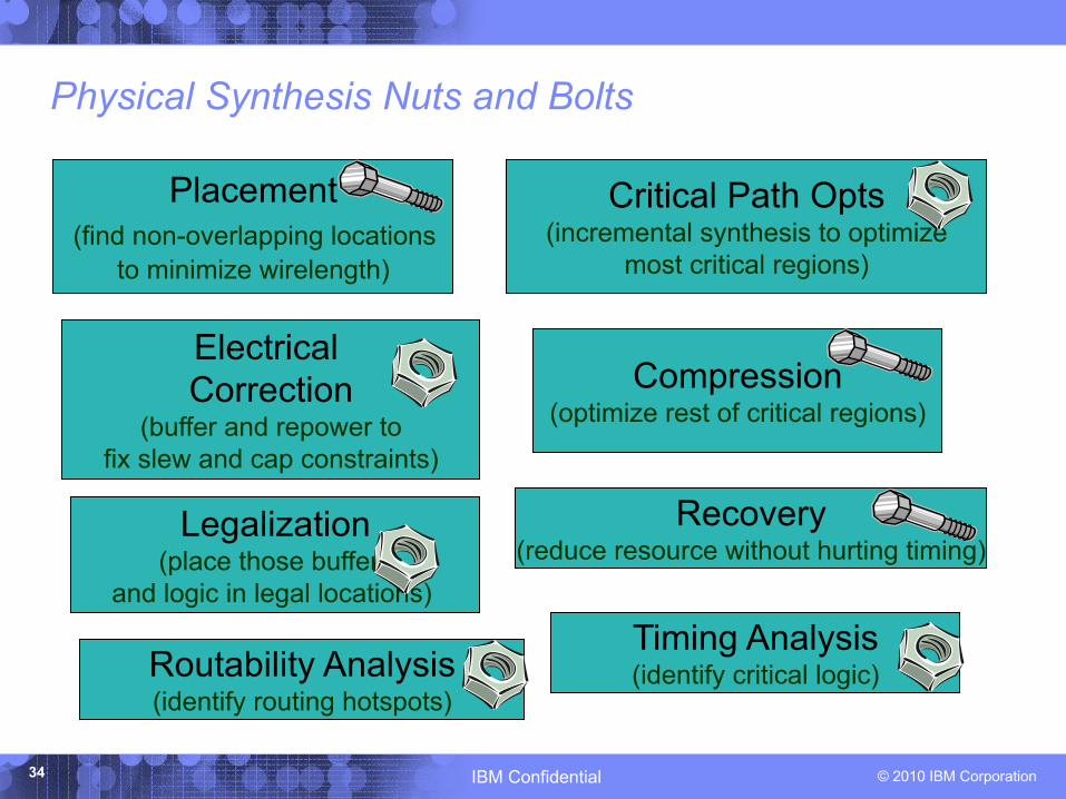
Physical Synthesis Nuts and Bolts
Placement(find non-overlapping locations
to minimize wirelength)
Electrical Correction
(buffer and repower tofix slew and cap constraints)
Timing Analysis(identify critical logic)
Legalization(place those buffers
and logic in legal locations)
Critical Path Opts(incremental synthesis to optimize
most critical regions)
Compression(optimize rest of critical regions)
Recovery(reduce resource without hurting timing)
Routability Analysis(identify routing hotspots)
© 2010 IBM CorporationIBM Confidential35
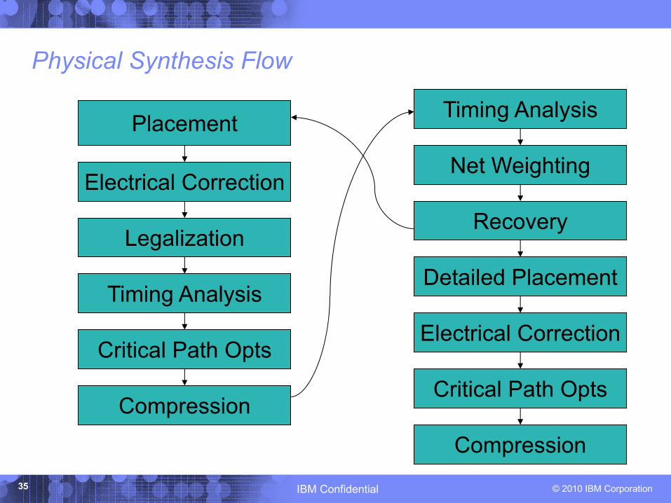
Physical Synthesis Flow
Placement
Electrical Correction
Legalization
Timing Analysis
Critical Path Opts
Compression
Timing Analysis
Net Weighting
Recovery
Detailed Placement
Electrical Correction
Critical Path Opts
Compression
© 2010 IBM CorporationIBM Confidential36
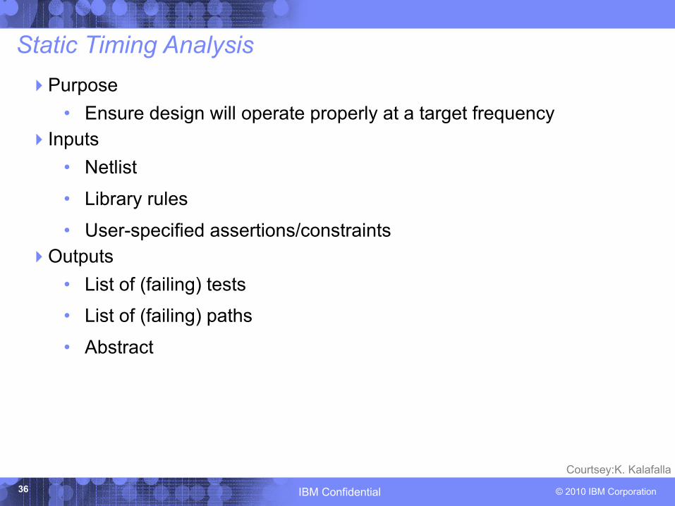
Static Timing Analysis4Purpose
• Ensure design will operate properly at a target frequency 4Inputs
• Netlist• Library rules• User-specified assertions/constraints
4Outputs• List of (failing) tests• List of (failing) paths• Abstract
Courtsey:K. Kalafalla
© 2010 IBM CorporationIBM Confidential37
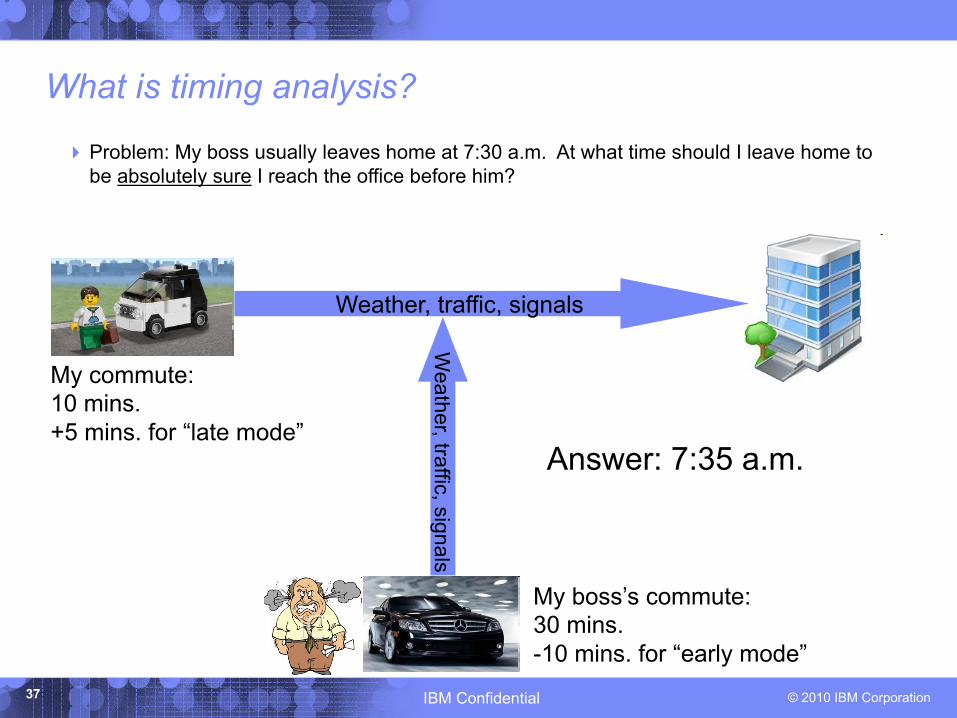
What is timing analysis?
4 Problem: My boss usually leaves home at 7:30 a.m. At what time should I leave home to be absolutely sure I reach the office before him?
Weather, traffic, signals
Weather, traffic, signals
My commute:10 mins.+5 mins. for “late mode”
My boss’s commute:30 mins.-10 mins. for “early mode”
Answer: 7:35 a.m.
© 2010 IBM CorporationIBM Confidential38
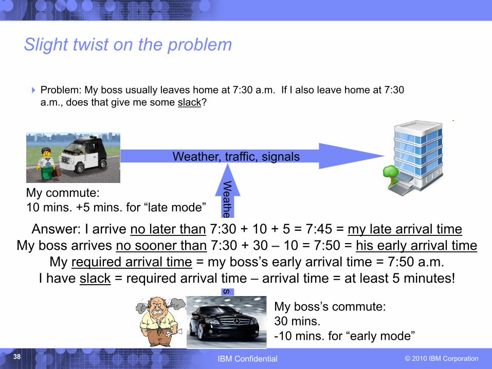
Slight twist on the problem
4 Problem: My boss usually leaves home at 7:30 a.m. If I also leave home at 7:30 a.m., does that give me some slack?
Weather, traffic, signals
Weather, traffic, signals
My commute:10 mins. +5 mins. for “late mode”
My boss’s commute:30 mins.-10 mins. for “early mode”
Answer: I arrive no later than 7:30 + 10 + 5 = 7:45 = my late arrival timeMy boss arrives no sooner than 7:30 + 30 – 10 = 7:50 = his early arrival time
My required arrival time = my boss’s early arrival time = 7:50 a.m.I have slack = required arrival time – arrival time = at least 5 minutes!
© 2010 IBM CorporationIBM Confidential39
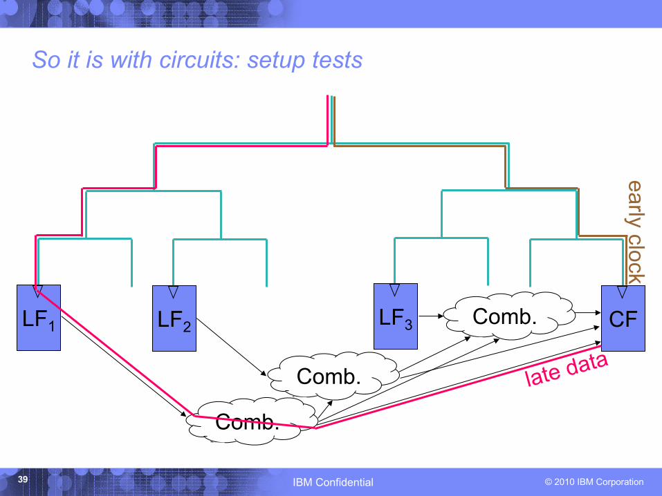
So it is with circuits: setup tests
LF1 LF2 CFLF3 Comb.
Comb.
Comb.
early clock
© 2010 IBM CorporationIBM Confidential40
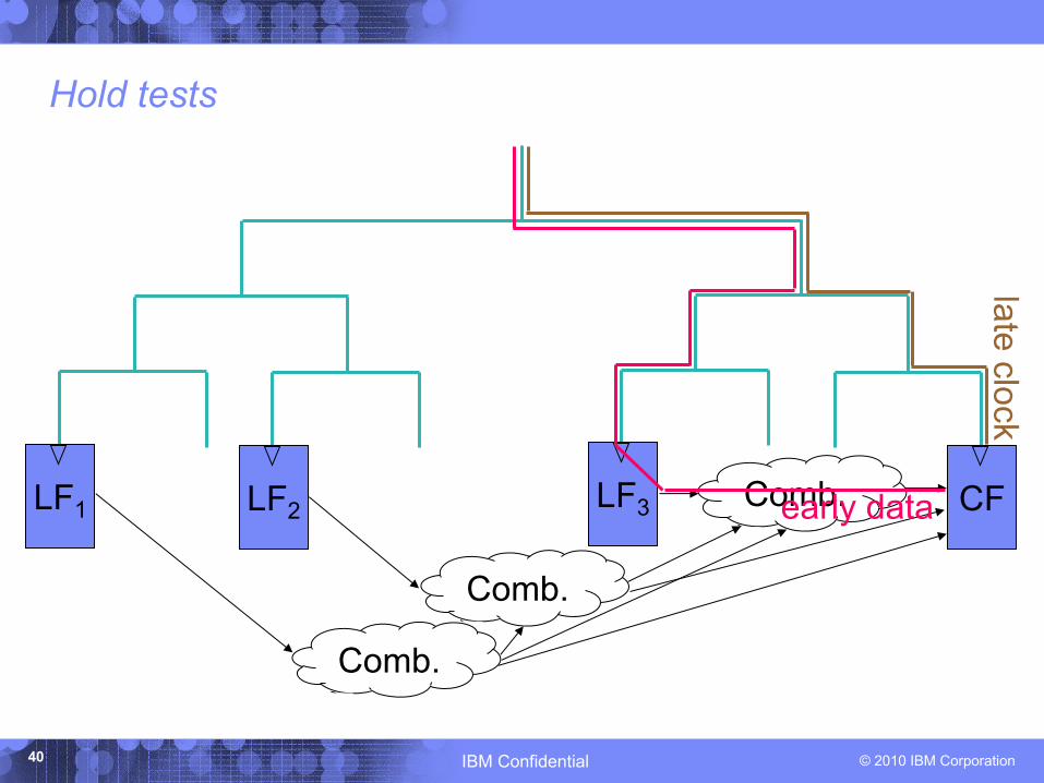
Hold tests
LF1 LF2 CFLF3 Comb.
Comb.
Comb.
early data
late clock

© 2010 IBM CorporationIBM Confidential41
Timing analysis of circuits
4With every signal, we associate four arrival times• Early (rise and fall)• Late (rise and fall)
4Late arrival time is 100 ps means, “if at all a signal switches in any given cycle, it will be stable after 100 ps”
4Early arrival time is 50 ps means, “if at all a signal switches in any given cycle, it will not change from its previous cycle stable value sooner than 50 ps”
4Setup test: compare late data arrival time to early clock4Hold test: compare early data arrival time to late clock4Requires just one simple pass of the circuit (or “timing
graph”);
© 2010 IBM CorporationIBM Confidential42
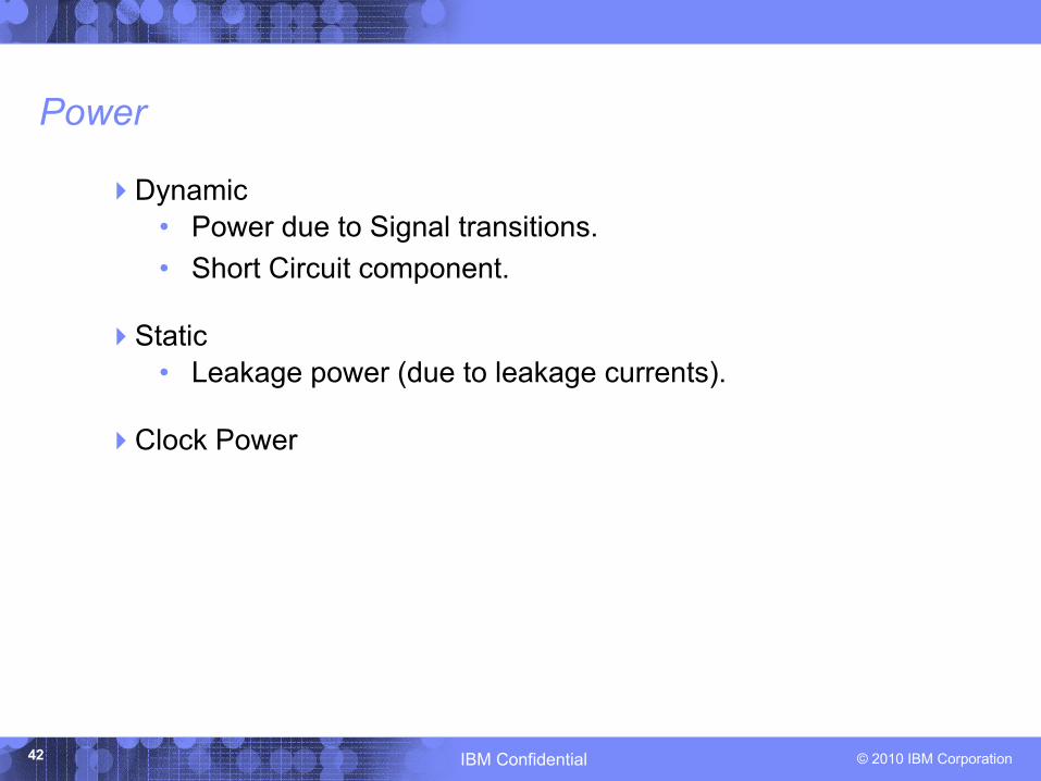
4Dynamic• Power due to Signal transitions. • Short Circuit component.
4Static • Leakage power (due to leakage currents).
4Clock Power
Power
© 2010 IBM CorporationIBM Confidential43
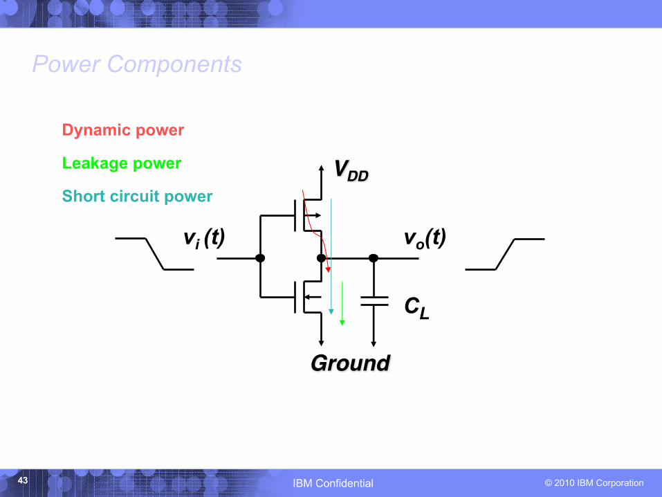
VDD
Ground
CL
vi (t) vo(t)
Dynamic power
Short circuit power
Leakage power
Power Components
© 2010 IBM CorporationIBM Confidential44
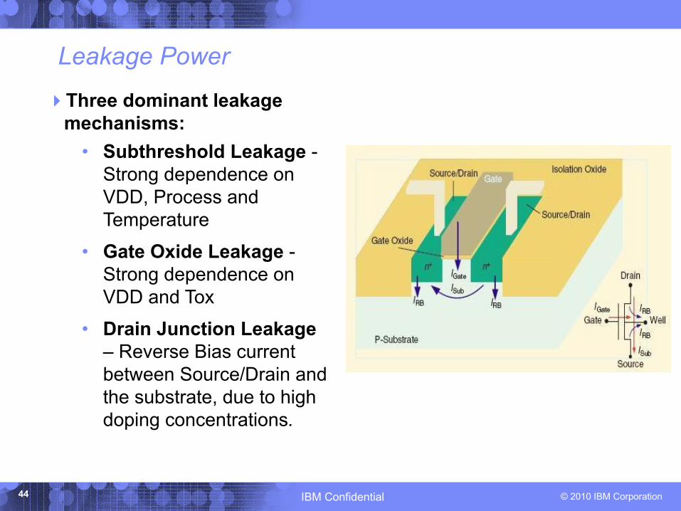
4Three dominant leakage mechanisms:
• Subthreshold Leakage -Strong dependence on VDD, Process and Temperature
• Gate Oxide Leakage -Strong dependence on VDD and Tox
• Drain Junction Leakage– Reverse Bias current between Source/Drain and the substrate, due to high doping concentrations.
Leakage Power
© 2010 IBM CorporationIBM Confidential45
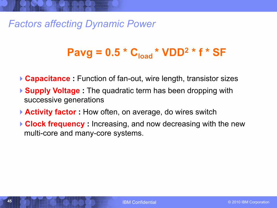
4Capacitance : Function of fan-out, wire length, transistor sizes4Supply Voltage : The quadratic term has been dropping with
successive generations4Activity factor : How often, on average, do wires switch4Clock frequency : Increasing, and now decreasing with the new
multi-core and many-core systems.
Factors affecting Dynamic Power
Pavg = 0.5 * Cload * VDD2 * f * SF

© 2010 IBM CorporationIBM Confidential46
Verification
ArchitectureSpecification
MicroArchitecture
Spec
LogicImplementation
(VHDL)
CircuitImplementation
DesignModel
Mathematical Equiv Proof(Formal Verification)
(100%)
VerificationStrategies
Goal : Find >98%Bugs pre-silicon
Courtsey:K. W. Roesner
© 2010 IBM CorporationIBM Confidential47
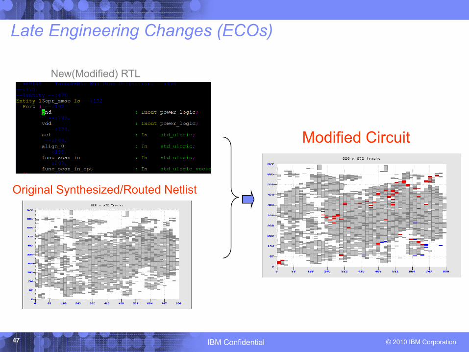
Late Engineering Changes (ECOs)
New(Modified) RTL
Original Synthesized/Routed Netlist
Modified Circuit
© 2010 IBM CorporationIBM Confidential
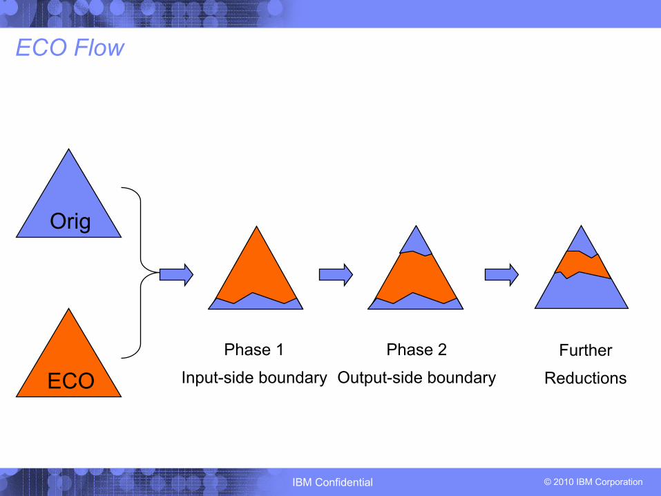
ECO Flow
Phase 2Output-side boundary
Phase 1Input-side boundary
FurtherReductionsECO
Orig

© 2010 IBM CorporationIBM Confidential49
Release to Manufacturing4 Final edits to the layout are made4 Metal fill and metal stress relief rules are checked4 Manufacturing information such as scribe lanes, seal rings, mask shop
data, part numbers, logos and pin 1 identification information for assembly are also added
4 DRC and LVS are run to verify the correctness of the modified database; Electrical rule checking;
4 ‘Tapeout’ documentation is prepared prior to release of the GDSII to the foundry
4 Pad location information is prepared, typically in a spreadsheet4 Custom-manual edits of the mask layers4 Manufacturing steps
• generation of masks; silicon processing; wafer testing; assembly and packaging; manufacturing test