Embed Size (px)
Citation preview
Design Considerations of
UFS & e.MMC Controllers
Compliance & Compatibility
© 2013 Arasan Chip Systems, Inc.
Y u p i n g C h u n g
Arasan Chip systems, Inc.
San Jose, CA
JEDEC Mobile Forum May 2013
Agenda
• Mobile Storage in SoC
• Challenges to Mobile Storage Controller Designs
• Enabling Mobile Storage Design Ecosystem
• Summary
5/2/2013 Page 2
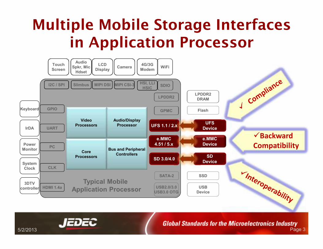
Multiple Mobile Storage Interfaces in Application Processor
Core
Processors
Bus and Peripheral
Controllers
Video
Processors
Audio/Display
Processor
LPDDR2LPDDR2
DRAM
SATA-2 SSD
Flash
USB2.0/3.0
USB3.0 OTG
USB
Device
MIPI CSI-3
Camera
MIPI DSI
LCD
Display
Slimbus
Audio
Spkr, Mic
Hdset
Keyboard
IrDA
Power
Monitor
System
Clock
GPIO
I2C / SPI
UART
PC
CLK
WiFi
HSI, LLI
HSIC
4G/3G
Modem
Typical Mobile
Application Processor
Touch
Screen
3DTV
controller HDMI 1.4a
GPMC
SDIO
UFS 1.1 / 2.xUFS
Device
SD 3.0/4.0SD
Device
e.MMC
4.51 / 5.x
e.MMC
Device
�Backward
Compatibility
5/2/2013 Page 3
Mobile Storage Evolution Faster Than Ever
5/2/2013
e.MMC 4.3
Boot-up
SD 2.0High
capacity
MMC 4.2
High
Capacity
Peaked
SD 3.0UHS-I
e.MMC 4.41
DDR
104MB/s
1,4-bit
Ramping
UpSD 4.0UHS II
1.56
Gbps
e.MMC 4.51
HS200
200MB/s
Serial
Differential
Early
AdopterSD 1.1High
speed
MMC 4.1
High Speed
Obsolete
SD 1.0Next
Gen
2006 2009 201220112003 2013
UFS 2.xUFS 1.1
e.MMC 5.x
SD
UFS
e.MMC
Page 4
UFS 1.0
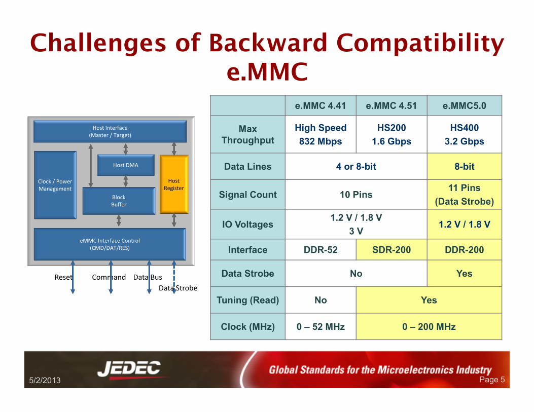
Challenges of Backward Compatibility e.MMC
5/2/2013
e.MMC 4.41 e.MMC 4.51 e.MMC5.0
Max
Throughput
High Speed
832 Mbps
HS200
1.6 Gbps
HS400
3.2 Gbps
Data Lines 4 or 8-bit 8-bit
Signal Count 10 Pins11 Pins
(Data Strobe)
IO Voltages1.2 V / 1.8 V
3 V1.2 V / 1.8 V
Interface DDR-52 SDR-200 DDR-200
Data Strobe No Yes
Tuning (Read) No Yes
Clock (MHz) 0 – 52 MHz 0 – 200 MHz
Page 5
Host Interface
(Master / Target)
Host
Register
Host DMA
Clock / Power
Management
Block
Buffer
eMMC Interface Control
(CMD/DAT/RES)
Data BusCommandReset
Data Strobe
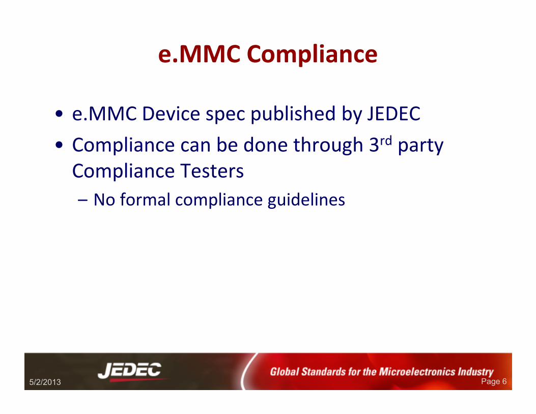
e.MMC Compliance
• e.MMC Device spec published by JEDEC
• Compliance can be done through 3rd party
Compliance Testers
– No formal compliance guidelines
5/2/2013 Page 6
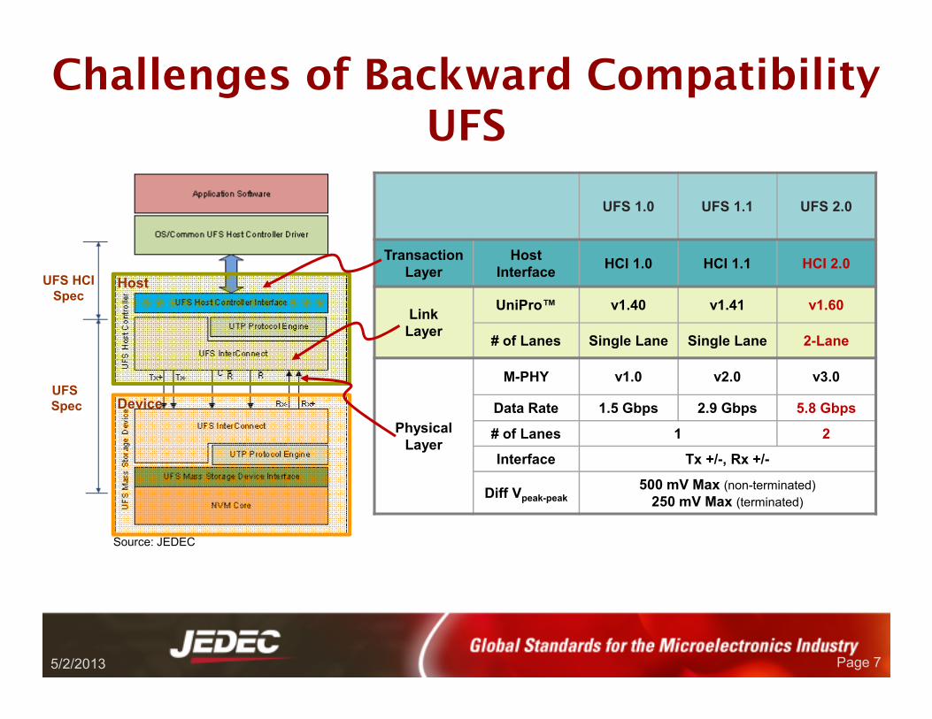
Challenges of Backward Compatibility UFS
5/2/2013
UFS 1.0 UFS 1.1 UFS 2.0
Transaction
Layer
Host
InterfaceHCI 1.0 HCI 1.1 HCI 2.0
Link
Layer
UniPro™ v1.40 v1.41 v1.60
# of Lanes Single Lane Single Lane 2-Lane
Physical
Layer
M-PHY v1.0 v2.0 v3.0
Data Rate 1.5 Gbps 2.9 Gbps 5.8 Gbps
# of Lanes 1 2
Interface Tx +/-, Rx +/-
Diff Vpeak-peak
500 mV Max (non-terminated)
250 mV Max (terminated)
Page 7
UFS HCI
Spec
UFS
Spec
Source: JEDEC
Host
Device
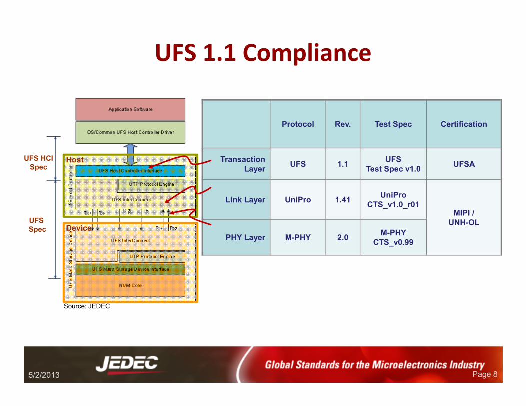
UFS 1.1 Compliance
Protocol Rev. Test Spec Certification
Transaction
LayerUFS 1.1
UFS
Test Spec v1.0UFSA
Link Layer UniPro 1.41UniPro
CTS_v1.0_r01MIPI /
UNH-OL
PHY Layer M-PHY 2.0M-PHY
CTS_v0.99
5/2/2013 Page 8
UFS HCI
Spec
UFS
Spec
Source: JEDEC
Host
Device
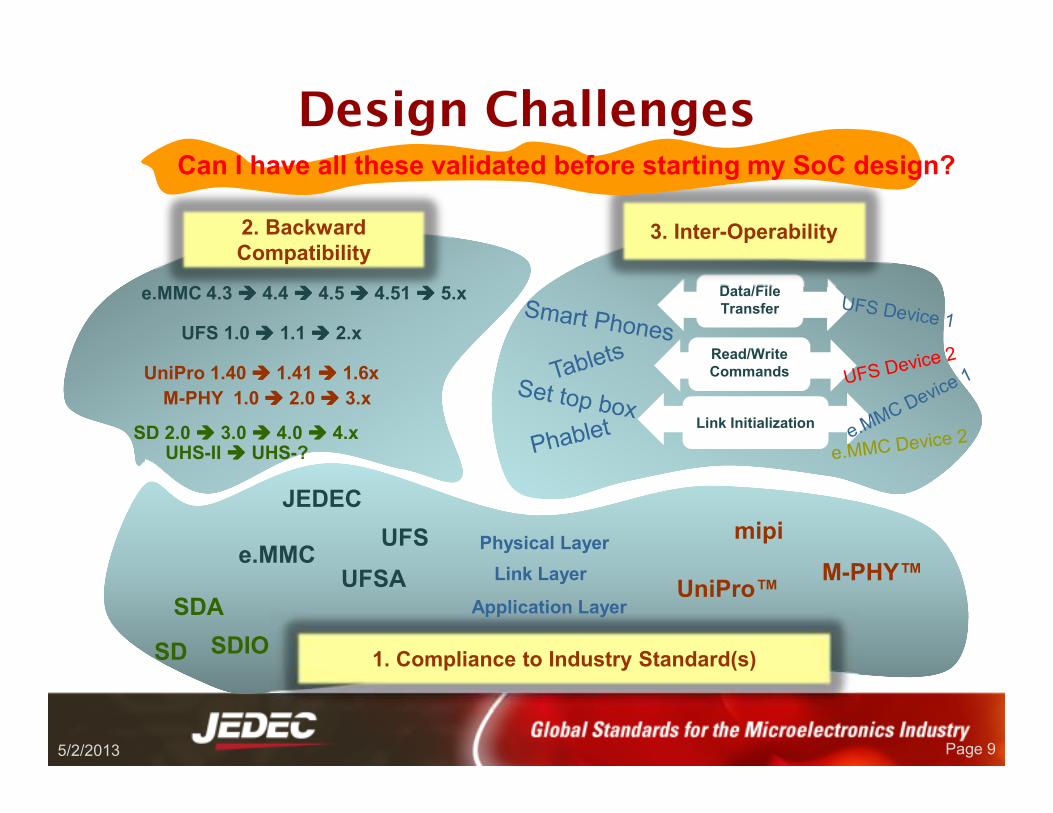
Design Challenges
5/2/2013 Page 9
1. Compliance to Industry Standard(s)
JEDEC
mipie.MMC
UFS
UniPro™M-PHY™
Physical Layer
Link Layer
Application LayerSDA
SD SDIO
UFSA
2. Backward
Compatibility
e.MMC 4.3 ���� 4.4 ���� 4.5 ���� 4.51 ���� 5.x
UFS 1.0 ���� 1.1 ���� 2.x
UniPro 1.40 ���� 1.41 ���� 1.6x
M-PHY 1.0 ���� 2.0 ���� 3.x
SD 2.0 ���� 3.0 ���� 4.0 ���� 4.xUHS-II ���� UHS-?
Data/File
Transfer
Read/Write
Commands
Link Initialization
3. Inter-Operability
Can I have all these validated before starting my SoC design?
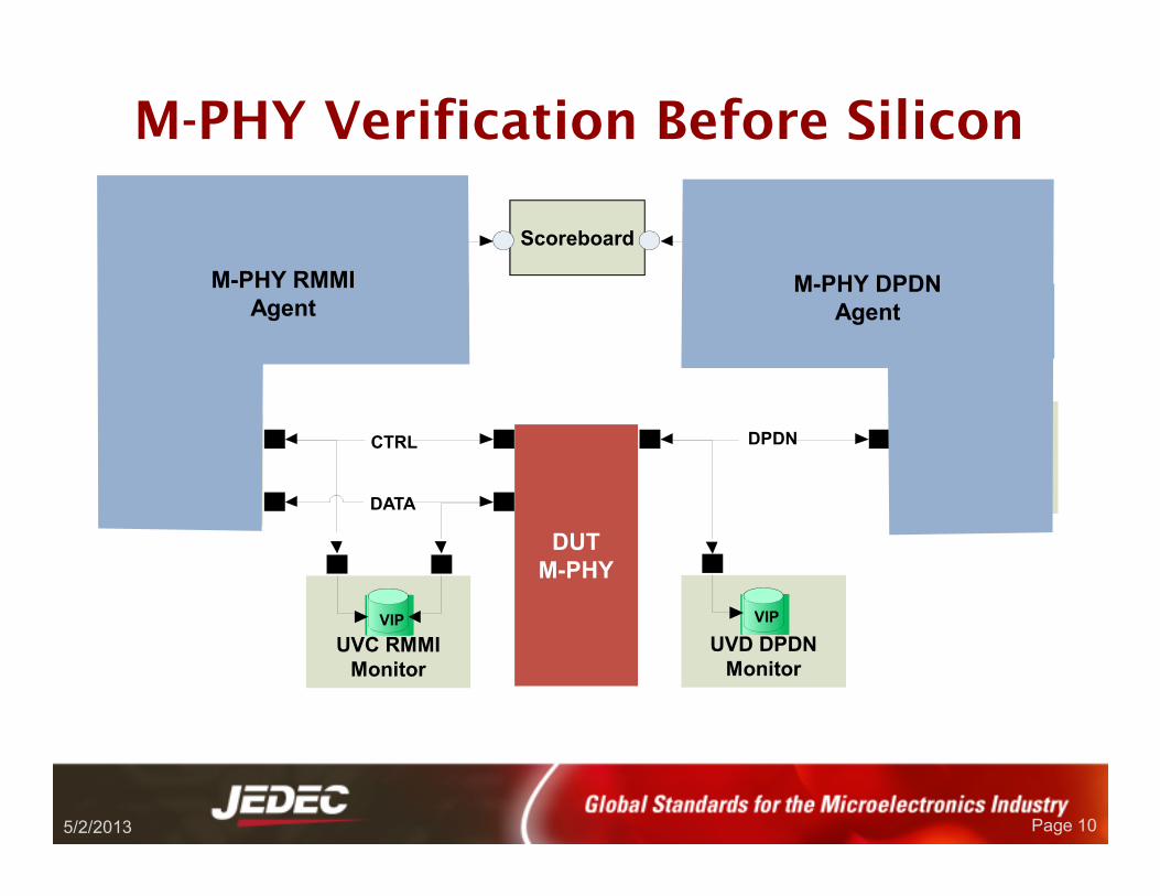
M-PHY Verification Before Silicon
5/2/2013 Page 10
DUT
M-PHY
UVC RMMI
Master
VIP
M-PHY
Agent
UVC RMMI
Monitor
VIP
UVC DPDN
VIP
UVD DPDN
Monitor
VIP
M-PHY
Agent
CTRL
DATA
DPDN
Sequencer SequencerScoreboard
CoverageCoverage
M-PHY RMMI
AgentM-PHY DPDN
Agent
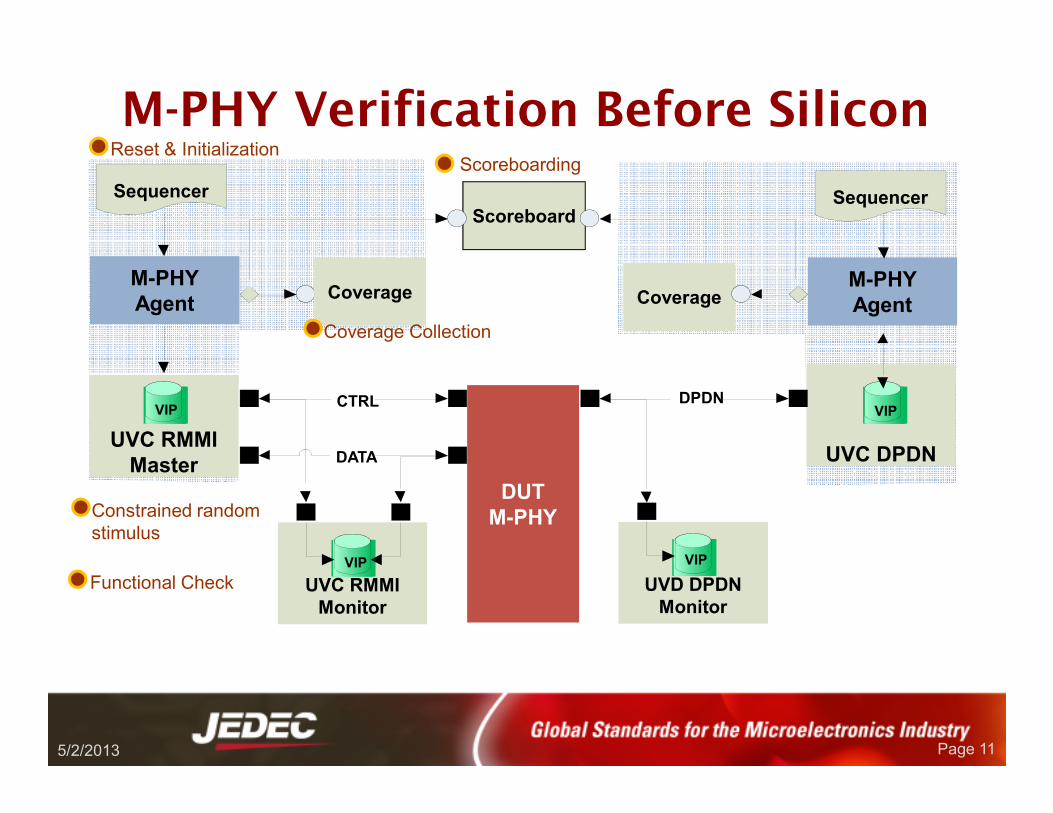
M-PHY Verification Before Silicon
5/2/2013 Page 11
DUT
M-PHY
UVC RMMI
Master
VIP
M-PHY
Agent
UVC RMMI
Monitor
VIP
UVC DPDN
VIP
UVD DPDN
Monitor
VIP
M-PHY
Agent
CTRL
DATA
DPDN
Sequencer SequencerScoreboard
CoverageCoverage
Reset & Initialization
Constrained random
stimulus
Functional Check
Coverage Collection
Scoreboarding
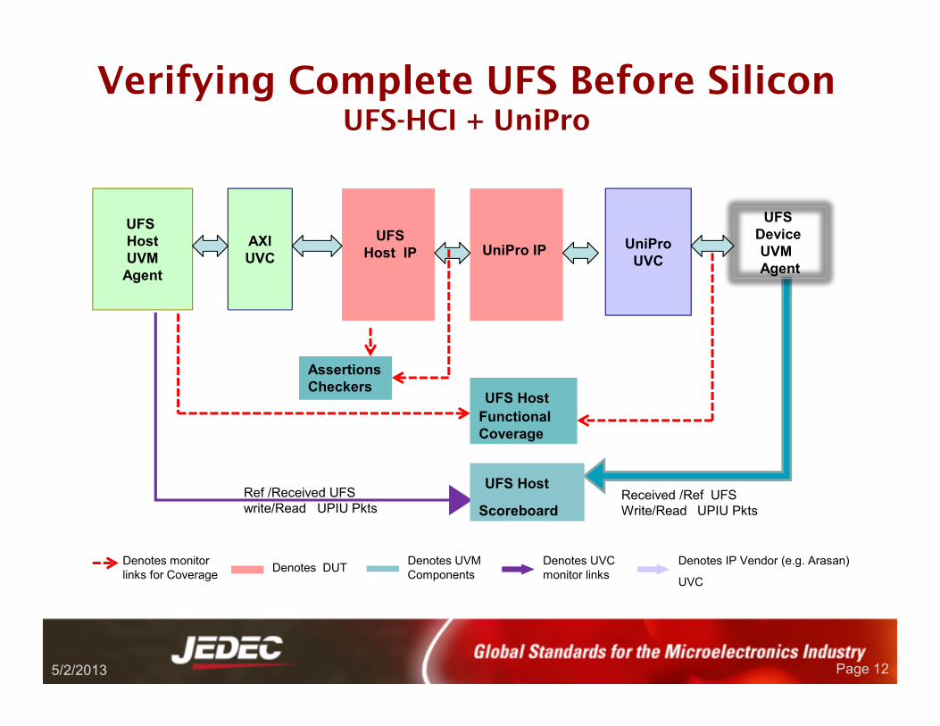
AXI
UVC
UFS
Host IP
UFS
Device
UVM
Agent
Ref /Received UFS
write/Read UPIU Pkts
UniPro IP UniPro
UVC
UFS Host
Scoreboard
UFS Host
Functional
Coverage
Received /Ref UFS
Write/Read UPIU Pkts
Assertions
Checkers
Denotes UVC
monitor links
Denotes UVM
ComponentsDenotes DUT
Denotes monitor
links for Coverage
UFS
Host
UVM
Agent
Denotes IP Vendor (e.g. Arasan)
UVC
Verifying Complete UFS Before SiliconUFS-HCI + UniPro
5/2/2013 Page 12
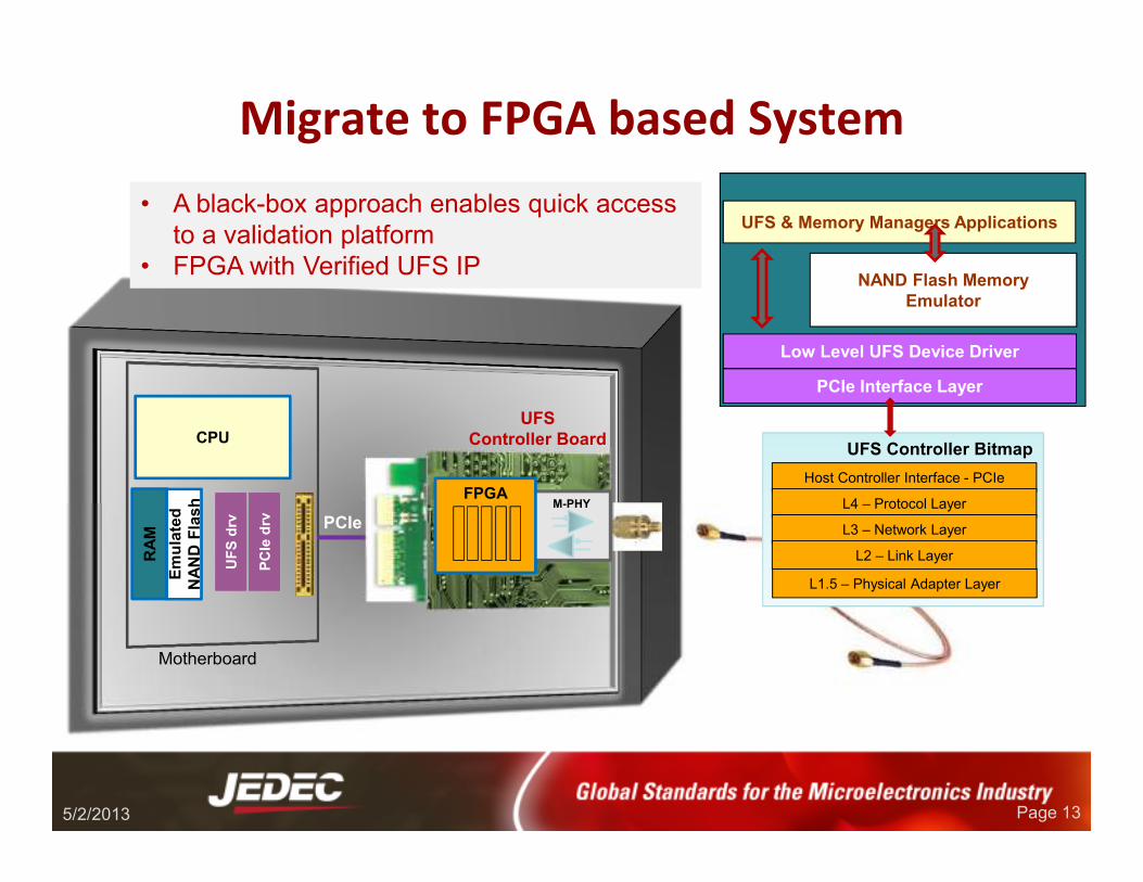
UFS Controller Bitmap
Migrate to FPGA based System
5/2/2013 Page 13
Motherboard
CPU
RAM
Host Controller Interface - PCIe
L4 – Protocol Layer
L3 – Network Layer
PCIe Interface Layer
Low Level UFS Device Driver
L2 – Link Layer
L1.5 – Physical Adapter Layer
PCIedrv
PCIedrv
UFS drv
UFS drv
NAND Flash Memory
Emulator
UFS & Memory Managers Applications
PCIe
Emulated
NAND Flash
UFS
Controller Board
M-PHYFPGA
• A black-box approach enables quick access
to a validation platform
• FPGA with Verified UFS IP
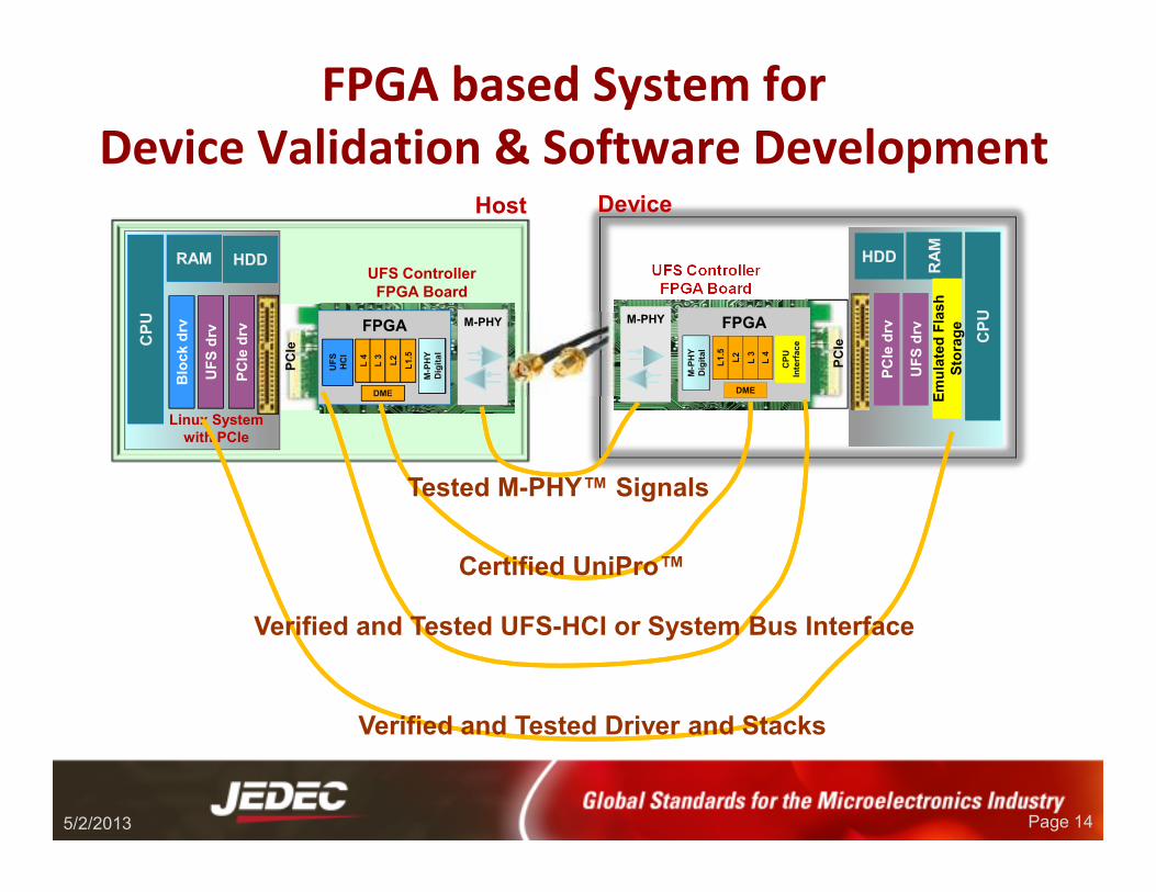
FPGA based System for
Device Validation & Software Development
UFS Controller
FPGA Board
CPU
RAMPCIedrv
Block drv
UFS drv
Linux System
with PCIe
M-PHYFPGAUFS
HCI
M-PHY
Digital
L 4
L 3
L2
L1.5
DME
HDD
PCIe
UFS Controller
FPGA Board
Linux System
with PCIe
M-PHY FPGA
CPU
Interface
CPU
Interface
M-PHY
Digital
L 4
L 3
L2
L1.5
DME
PCIe
CPU
RAM
PCIedrv
PCIedrv
UFS drv
UFS drv
HDD
Emulated Flash
Storage
Host Device
5/2/2013 Page 14
Tested M-PHY™ Signals
Certified UniPro™
Verified and Tested UFS-HCI or System Bus Interface
Verified and Tested Driver and Stacks
Enabling UFS/e.MMC Design Ecosystem
• FPGA based Development Platform productized into Validation
Platform
– IP, software stacks and PHY come together
• Used by IP vendor (eg. Arasan) for Interoperability testing with
other pioneers
• Used by Test & Measurement vendors as target platforms
– For validation of protocol generators and analyzers
• Ultimately used by SoC/Device vendors as target or reference
platforms for silicon validation
– Assured of IP interoperability, compliance, and backward compatibility
5/2/2013 Page 15
Summary• New JEDEC storage standards continue to evolve for new
markets
– Early IP/SoC validation enables compliance and compatibility for fast
time-to-market
• Different SoC vendors at different stages of spec adoption
– Different spec revisions from different OEM’s
– Backward compatibility and Interoperability a must among vendors
• IP vendors continue to
– Leading the pack to invest in transforming specs to RTL and GDSII
– Keeping Backward Compatibility with older standards in new designs
– Enabling ecosystem-wide Inter-op and Compliance through
• Software stacks
• Hardware Validation Platforms
5/2/2013 Page 16
All these are made available before starting your SoC/Device designs !!
THANK YOU
Design for Compliance and Compatibility
© 2013 Arasan Chip Systems, Inc.JEDEC Mobile Forum May 2013