Embed Size (px)
Citation preview
1
Design and Simulation of Voltage-Mode and Current-Mode
Class-D Power Amplifiers for 2.4 GHz Applications
Armindo António Barão da Silva Pontes
Abstract – This paper presents the design
and simulations of a voltage-mode class-D
(VMCD) and current-mode class-D (CMCD)
power amplifiers at 2.4 GHz. The amplifiers
were designed on AMS CMOS 0.35µm
technology which has 4 metal and 2 poly layers.
Comparisons and improvements are shown
via simulations for both amplifiers and for a
VMCD prototype already fabricated and
measured prior to this work. The main design
goals are the achievement of high efficiency
and power delivered to the load.
I. INTRODUCTION
One of the main requirements in a mobile
communication system is the low energy
consumption. For that switched-mode power
amplifiers are more interesting solutions than
linear classes. Here, the study and design
supported by simulations for the voltage-mode
class D (VMCD) and the current-mode class-D
switched power amplifiers is performed. The
amplifiers were implemented on AMS CMOS
0.35µm technology for 2.4GHz applications.
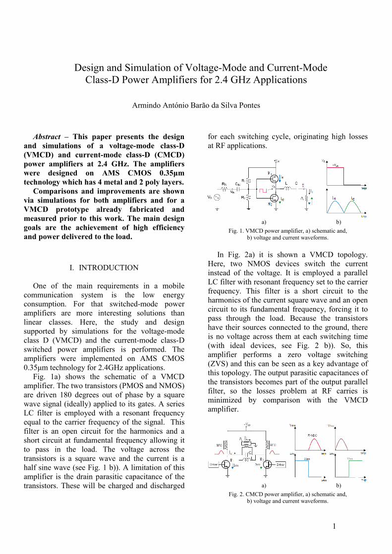
Fig. 1a) shows the schematic of a VMCD
amplifier. The two transistors (PMOS and NMOS)
are driven 180 degrees out of phase by a square
wave signal (ideally) applied to its gates. A series
LC filter is employed with a resonant frequency
equal to the carrier frequency of the signal. This
filter is an open circuit for the harmonics and a
short circuit at fundamental frequency allowing it
to pass in the load. The voltage across the
transistors is a square wave and the current is a
half sine wave (see Fig. 1 b)). A limitation of this
amplifier is the drain parasitic capacitance of the
transistors. These will be charged and discharged
for each switching cycle, originating high losses
at RF applications.
a) b)
Fig. 1. VMCD power amplifier, a) schematic and,
b) voltage and current waveforms.
In Fig. 2a) it is shown a VMCD topology.
Here, two NMOS devices switch the current
instead of the voltage. It is employed a parallel
LC filter with resonant frequency set to the carrier
frequency. This filter is a short circuit to the
harmonics of the current square wave and an open
circuit to its fundamental frequency, forcing it to
pass through the load. Because the transistors
have their sources connected to the ground, there
is no voltage across them at each switching time
(with ideal devices, see Fig. 2 b)). So, this
amplifier performs a zero voltage switching
(ZVS) and this can be seen as a key advantage of
this topology. The output parasitic capacitances of
the transistors becomes part of the output parallel
filter, so the losses problem at RF carries is
minimized by comparison with the VMCD
amplifier.
a) b)
Fig. 2. CMCD power amplifier, a) schematic and,
b) voltage and current waveforms.
2
In the CMCD amplifier were used two choke
inductors for biasing the transistors. The load
voltage amplitude depends linearly on the supply
voltage, VL=VDD/π. This permits that an amplitude
modulation can be created in the output signal
through the supply voltage. Simultaneously, an
existing phase modulation in the input RF signal
will appear at the output signal.
Also the choke inductors constitute an
advantage over current sources bias, because the
later isolates the supply voltage value from the
rest of the circuit.
II. AMPLIFIERS DESIGN
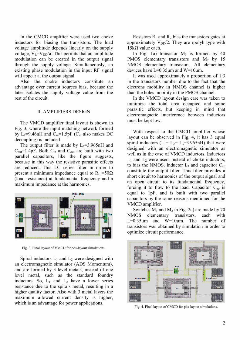
The VMCD amplifier final layout is shown in
Fig. 3, where the input matching network formed
by L1=9.46nH and Cin=1.5pF (Cin also makes DC
decoupling) is included.
The output filter is made by L2=3.965nH and
Cout=1.4pF. Both Cin and Cout are built with two
parallel capacitors, like the figure suggests,
because in this way the resistive parasitic effects
are reduced. This LC series filter in order to
present a minimum impedance equal to RL =50Ω
(load resistance) at fundamental frequency and a
maximum impedance at the harmonics.
Fig. 3. Final layout of VMCD for pos-layout simulations.
Spiral inductors L1 and L2 were designed with
an electromagnetic simulator (ADS Momentum),
and are formed by 3 level metals, instead of one
level metal, such as the standard foundry
inductors. So, L1 and L2 have a lower series
resistance due to the spirals metal, resulting in a
higher quality factor. Also with 3 metal layers the
maximum allowed current density is higher,
which is an advantage for power applications.
Resistors R1 and R2 bias the transistors gates at
approximately VDD/2. They are rpolyh type with
15kΩ value each.
In Fig. 1a) transistor M1 is formed by 40
PMOS elementary transistors and M2 by 15
NMOS elementary transistors. All elementary
devices have L=0.35µm and W=10µm.
It was used approximately a proportion of 1:3
in the transistors number due to the fact that the
electrons mobility in NMOS channel is higher
than the holes mobility in the PMOS channel.
In the VMCD layout design care was taken to
minimize the total area occupied and some
parasitic effects, but keeping in mind that
electromagnetic interference between inductors
must be kept low.
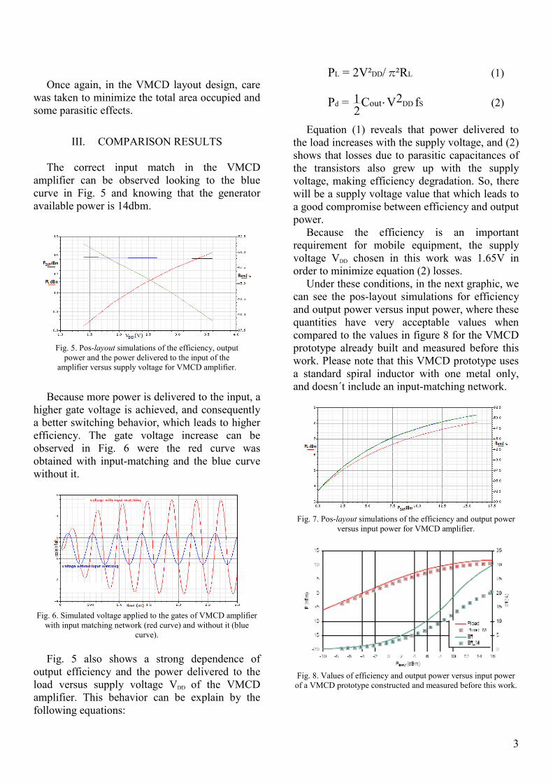
With respect to the CMCD amplifier whose
layout can be observed in Fig. 4, it has 3 equal
spiral inductors (L1= L2= L3=3.965nH) that were
designed with an electromagnetic simulator as
well as in the case of VMCD inductors. Inductors
L1 and L2 were used, instead of choke inductors,
to bias the NMOS. Inductor L3 and capacitor Cap
constitute the output filter. This filter provides a
short circuit to harmonics of the output signal and
an open circuit to its fundamental frequency,
forcing it to flow to the load. Capacitor Cap is
equal to 1pF, and is built with two parallel
capacitors by the same reasons mentioned for the
VMCD amplifier.
Switches M1 and M2 in Fig. 2a) are made by 70
NMOS elementary transistors, each with
L=0.35µm and W=10µm. The number of
transistors was obtained by simulation in order to
optimize circuit performance.
Fig. 4. Final layout of CMCD for pós-layout simulations.
3
Once again, in the VMCD layout design, care
was taken to minimize the total area occupied and
some parasitic effects.
III. COMPARISON RESULTS
The correct input match in the VMCD
amplifier can be observed looking to the blue
curve in Fig. 5 and knowing that the generator
available power is 14dbm.
Fig. 5. Pos-layout simulations of the efficiency, output
power and the power delivered to the input of the
amplifier versus supply voltage for VMCD amplifier.
Because more power is delivered to the input, a
higher gate voltage is achieved, and consequently
a better switching behavior, which leads to higher
efficiency. The gate voltage increase can be
observed in Fig. 6 were the red curve was
obtained with input-matching and the blue curve
without it.
Fig. 6. Simulated voltage applied to the gates of VMCD amplifier
with input matching network (red curve) and without it (blue
curve).
Fig. 5 also shows a strong dependence of
output efficiency and the power delivered to the
load versus supply voltage VDD of the VMCD
amplifier. This behavior can be explain by the
following equations:
L DD LP = 2V² / ²Rπ (1)
d DD Sout 21P = C V f2
⋅ (2)
Equation (1) reveals that power delivered to
the load increases with the supply voltage, and (2)
shows that losses due to parasitic capacitances of
the transistors also grew up with the supply
voltage, making efficiency degradation. So, there
will be a supply voltage value that which leads to
a good compromise between efficiency and output
power.
Because the efficiency is an important
requirement for mobile equipment, the supply
voltage VDD chosen in this work was 1.65V in
order to minimize equation (2) losses.
Under these conditions, in the next graphic, we
can see the pos-layout simulations for efficiency
and output power versus input power, where these
quantities have very acceptable values when
compared to the values in figure 8 for the VMCD
prototype already built and measured before this
work. Please note that this VMCD prototype uses
a standard spiral inductor with one metal only,
and doesn´t include an input-matching network.
Fig. 7. Pos-layout simulations of the efficiency and output power
versus input power for VMCD amplifier.
Fig. 8. Values of efficiency and output power versus input power
of a VMCD prototype constructed and measured before this work.
4
In the case of CMCD amplifier, if we compare
Fig. 9 (amplifier simulated with ideal inductors)
with Fig. 10 (pos-layout simulations with
electromagnetic simulated spiral inductors), we
can see a reduction in efficiency and in output
power due to the losses in spiral inductors, mainly
the two spiral inductors, L1 and L2, which bias the
transistors.
Fig. 9. Simulations of the efficiency and the power delivered to the
load versos input power with ideal spiral inductors for CMCD
amplifier.
It should be studied a better solution in order to
minimize the losses of these two spiral inductors,
e.g., implementing these components with
bondwires, because bondwires have wider cross-
sections resulting in smaller parasitic resistance.
This CMCD amplifier can achieve better
performance for efficiency and output power in
contrast to VMCD at RF frequencies.
Fig. 10. Pos-layout simulations of the efficiency and output power
versus input power for CMCD amplifier.
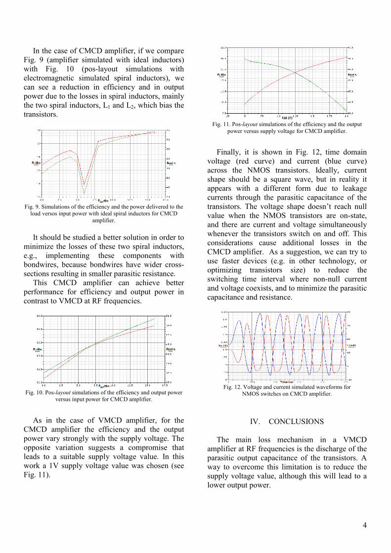
As in the case of VMCD amplifier, for the
CMCD amplifier the efficiency and the output
power vary strongly with the supply voltage. The
opposite variation suggests a compromise that
leads to a suitable supply voltage value. In this
work a 1V supply voltage value was chosen (see
Fig. 11).
Fig. 11. Pos-layout simulations of the efficiency and the output
power versus supply voltage for CMCD amplifier.
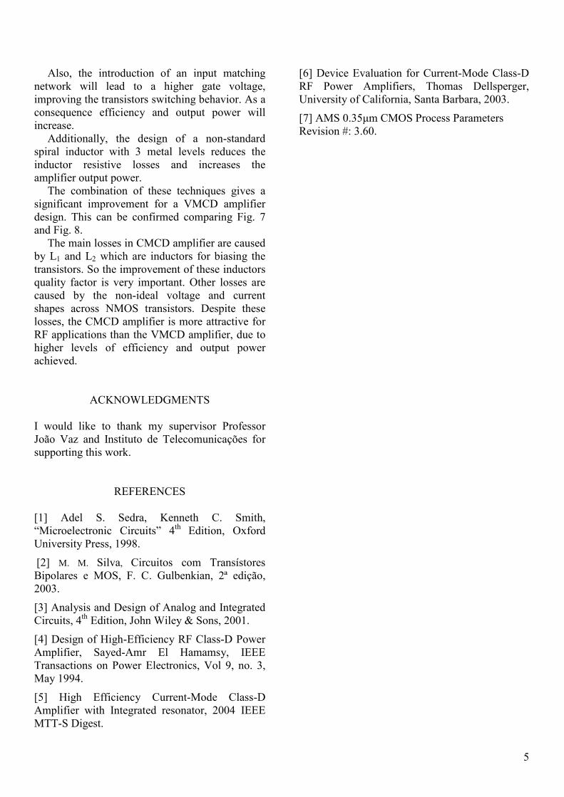
Finally, it is shown in Fig. 12, time domain
voltage (red curve) and current (blue curve)
across the NMOS transistors. Ideally, current
shape should be a square wave, but in reality it
appears with a different form due to leakage
currents through the parasitic capacitance of the
transistors. The voltage shape doesn’t reach null
value when the NMOS transistors are on-state,
and there are current and voltage simultaneously
whenever the transistors switch on and off. This
considerations cause additional losses in the
CMCD amplifier. As a suggestion, we can try to
use faster devices (e.g. in other technology, or
optimizing transistors size) to reduce the
switching time interval where non-null current
and voltage coexists, and to minimize the parasitic
capacitance and resistance.
Fig. 12. Voltage and current simulated waveforms for
NMOS switches on CMCD amplifier.
IV. CONCLUSIONS
The main loss mechanism in a VMCD
amplifier at RF frequencies is the discharge of the
parasitic output capacitance of the transistors. A
way to overcome this limitation is to reduce the
supply voltage value, although this will lead to a
lower output power.
5
Also, the introduction of an input matching
network will lead to a higher gate voltage,
improving the transistors switching behavior. As a
consequence efficiency and output power will
increase.
Additionally, the design of a non-standard
spiral inductor with 3 metal levels reduces the
inductor resistive losses and increases the
amplifier output power.
The combination of these techniques gives a
significant improvement for a VMCD amplifier
design. This can be confirmed comparing Fig. 7
and Fig. 8.
The main losses in CMCD amplifier are caused
by L1 and L2 which are inductors for biasing the
transistors. So the improvement of these inductors
quality factor is very important. Other losses are
caused by the non-ideal voltage and current
shapes across NMOS transistors. Despite these
losses, the CMCD amplifier is more attractive for
RF applications than the VMCD amplifier, due to
higher levels of efficiency and output power
achieved.
ACKNOWLEDGMENTS
I would like to thank my supervisor Professor
João Vaz and Instituto de Telecomunicações for
supporting this work.
REFERENCES
[1] Adel S. Sedra, Kenneth C. Smith,
“Microelectronic Circuits” 4th
Edition, Oxford
University Press, 1998.
[2] M. M. Silva, Circuitos com Transístores
Bipolares e MOS, F. C. Gulbenkian, 2ª edição,
2003.
[3] Analysis and Design of Analog and Integrated
Circuits, 4th
Edition, John Wiley & Sons, 2001.
[4] Design of High-Efficiency RF Class-D Power
Amplifier, Sayed-Amr El Hamamsy, IEEE
Transactions on Power Electronics, Vol 9, no. 3,
May 1994.
[5] High Efficiency Current-Mode Class-D
Amplifier with Integrated resonator, 2004 IEEE
MTT-S Digest.
[6] Device Evaluation for Current-Mode Class-D
RF Power Amplifiers, Thomas Dellsperger,
University of California, Santa Barbara, 2003.
[7] AMS 0.35µm CMOS Process Parameters
Revision #: 3.60.