Embed Size (px)
Citation preview

SLAC-PUB-5906 - - -us. SLD-NOTE-217 .
March 1992 WI)
Design and Performance of the SLD Vertex Detector, a 120 MP ixel Tracking System’
G D Agnewl, i &ttod, C J S Damerel12, R L English2, A R Gilbnan2, S J Hedge& J Hoeflich3, A L wntm2, L M&~Y&, A K ~~Kemeyl, A Nichol$, G D Punka?, J Richman4, Rang Gang2b, R S@phenson2, M G Stmuss5,
. . Su Dong2, G J R Tappem2, S J Wattsl, F J Wickens
1. Brunei University, Uxbridge, Middlesex, UK.
2. Rutherford &&on Laboratory, Chilton, Didcot, Oxon, UK. _~
3. - Stanford Linear Accelerator Center, Stanford University, Stanford, CA 94309 .
4.,. ~. UC Santa Barbara, CA 93106, USA. - -
5: - University of Massachusetts, Amherst, MA 01003, USA.
a. Present address: Metrolab, Geneva CH1228, Switzerland.
b. Fresent address: institute of High Energy Physics, Beijing, China.
Paper contributed to the XXVI International Conference on High Energy Physics Dallas, Texas, 6 - 12 August 1992
l This work was supported by the Qirector, Office of Energy Research, Office of High Energy and Nuclear Physics, Division of High Energy Physics,
of the U.S. Department of Energy under Contract No. DE-ACO3-76SFQO515 and by the U.K. Science and Engineming Research Council

- - s-.-
Design and Performance of the SLD Vertex Detector, a 120 MPixel Tracking System
G D Agnew, R Cotton, C J S Damerell, R L English, A R Gillman, S J Hedges, J Hoeflich, A L Lintem, L Mathys, A K McKemey, A Nichols, G D Punkar, J Richman, Rong Gang, R Stephenson, M G Strauss, Su Dong,
G J R Tappem, S J Watts, F J Wickens.
Abstraci This paper describes the design, construction, and initial operation of the SLD Vertex Detector, the first device to employ charge coupled devices (CCDs) on a large scale in a high energy physics experiment. The Vertex Detector comprises 4czo_CCDs, with a total of 120 Mpixels. Each pixel fun&ons as an independent particle detecting element, providing space point measurements of charged particle tracks with a typical precision of
I 5 pm in each co-ordinate. The CCDs are arranged in four concentric cylinders just outside the beam pipe which surrounds the e+e- collision point of the SLAC Linear Collider (SLC). The Vertex Detector is a powerful tool for distinguishing secondary vertex tracks, produced by decay in flight of heavy flavour hadrons or tau leptons, from tracks produced at the .~ primary event vertex. Because the colliding beam environment- imposes severe constraints on the design of such a detector, a six year R&D progmmme~was needed to develop solutions to a number of problems. The requirements include a low-mass structure (to minim& multiple scattering) both for mechanical support and to provide signal paths for the CCDs; operation at low temperature with a high degree of mechanical stability; and relatively high speed CCD readout, signal processing, and data sparsification. The lessons learned through the long R&D period should be useful for the construction of large arrays of CCDs or smart pixel devices in the future, in a number of
i- areas of science and technology.
1. Introduction and Overview
In response to the discovery of particles containing heavy flavour quarks (charm and bottom) which have lifetimes (as it turned out) in the
- region 1@ *3-1(r12 seconds, several groups in the late 70s worked intensively to develop electronic tracking detectors with the precision necessary to disentangle the primary and secondary vertices in the production and decay of these heavy flavour particles. As a result of a feasibility study [l I it was
_ I- concluded in 1981 that 2-dimensional charge cou Ied devices (CCDs) might be suitable for this pui s *se. Th<s study was followed by experimental work in a CERN test beam, where by 1983 the efficiency and precision (about 5 Frn space.points) of CCDs for tracking minimum-ionising particles was demonstrated [2]. This was followed by the use of two CCDs placed immediately after a compact solid target illuminated by a 200 GeV/c particle beam at the front end of the ACCMOR spectrometer at the
Fig. 1 One of the 480 CCDs of the Detector.
SPS in CERN. This set-up led to many physics papers based on the reconstruction of charm decays clearly separated from the primary vertices. The first of these was published 131 in 1987, and subsequent papers included the shortest measured lifetime of any charm particle [4], the Z’,, at 0.8 x lo-l3 seconds. While this experiment established the capability of CCD detectors for doing physics with short-lived particles, it was performed under particularly favourable conditions. Firstly, the entire acceptance of the multi-particle spectrometer was covered by less than 1 cm2 o f active vertex detector, and secondly the secondary particle momenta were sufficiently high that multiple scattering was not generally a problem.
Table 1 VXD Physical Parameters
Component Radius Thickness 1
Ream-pipe (mm) L/l-R (so) 25.5 0.283
Gas shell 27.0 0.142 Barrel 1 (13 ladders) 29.5 1.064 Barrel 2 (13 ladders) 33.5 1.064 Barrel 3 (17 ladders) 37.5 1.064 Barrel 4 (17 ladders) 41.5 1.064 Support Shell 45.5 0.387 Gas 0.057 Cryostat 165.5 0.698 *Effective Total 4.0 ‘A track on average goes through 2.3 ladders
1

Fig. 2 Ladder comprising a mother card and 8 CCDs.
In the present paper, we report the results of the next (and much more challenging) step in the evolution of CCDs as particle tracking detectors. Plans for this work were first published 151 in 1987, and brief status reports have subsequently appeared in_t_he proceedings of various conferences.
The first complication in this detector design was the need for good solid angle coverage in the
. . laboratory co-ordinate system (since the Z% produced by e+e- annihilation are at rest and their decay products fly out in all directions). The next complication was that, as a result of experience with backgrounds in the Mark 11 Detector in SLC, it was necessary to enlarge the planned ‘SLD beam-pipe radius from 10 to 25 mm. These two factors increased the number of CCDs required from two (in the. fixed t-a~get experiment) to 480. The collider environment is in any case more difficult than that of P fixed target experiment because of the need to mini&e the extraneous material in all directions (mechanical supports, local electronics, cabling, plumbing, etc.). Because access for servicing the innermost detector is extremely restricted, reliability of the detector and local equipment is of great importance. Fortunately, as is reported in this paper, solutions were found to these problems, and in so doing it has been possible to establish the feasibility of large mosaics of CCDs for high
Fig. 4 Inner section of SLC Beam-pipe.
precision particle tracking over a large area and/or solid angle. The lessons learned in the long R&D phase of this project will (we hope) be of use to others interested in building large CCD mosaics for work in other areas of science as well as for future applications in particle physics.
An overview of the Vertex Detector is best given with the aid of a series of photographs which more or less chronologically follow the production of the detector and its installation in SLD. Fig. 1 shows one of the CCDs wire bonded to a mother card. The CCD contains approximately 400x600 pixels each of size 22x22 Km; active area approximately 9x13 mm. Fig. 2 shows an 8-CCD ladder. The CCDs on the underside fill the gaps between those on top, giving continuous coverage over an area of 9x100 mm. Fig. 3 shows the two halves of the overall Vertex Detector (VXD), comprising four concentric barrels with 60 ladders in total (120 Mpixels). Some of the important physical parameters are listed in Table 1. Note that
Fig. 3 The upper and lower modules of the complete Vertex Detector (60 ladders). The scale can be judged from the active length of each ladder (100 mm) and radius of Barrel 1 (29.5 mm).
2

Fia 5 North section of inner beam-pipe with the support cone and mask M3 being assembled.
a. the effective barrel thicknesses are lower than the listed ladder values, due to the gaps between ladders. The two detector modules were eventually clamped together to form a rigid cylindrical structure which was stably mounted via a spring- loaded 3-point kinematic mount to the inner section of the SLC beam-pipe. The beam-pipe is shown in
_ _. fig. 4; the e+e- interaction point (IP) is at the centre of.t.he region photographed. We shall in general use the SLD co-ordinate system, which has the origin at the !P,-the Z axis being the positron beam axis (runnjng~from South to North, or right to left in the figure), the Y axis being vertically up, and the X axis horizontal, making a right-handed system. The innermost section of beam-pipe (seen to be darker in the figure) is a beryllium tube, to which are brazed short stainless steel sections which carry the wire movers (motors used to traverse fine X and Y wires in to the centre of the beam-pipe for beam tuning). Beyond the wire movers are circular plates which during assembly are clamped to support arches.
.-- Immediately beyond these plates, the beam-pipe is .. made non-rigid by a system of bellows which can be
seen in fig. 5. Here the support arches are being _ replaced by support cones, which -will eventually be
used to couple the inner beam-pipe to the Central Drift Chamber (CDC). Between the support cone and the beam-pipe (also conical in this region) one
- can see the lower half of M3, a tungsten mask which
Fig. 6 North support cone complete.
- Fig. 7 Vertex Detector mounted on the beam-
pipe, with local electronics. This photograph covers most of the 2 m length of the R20 module.
forms the last major line of defence of the SLD detector against SLC-generated background. This assembly is completed in fig. 6. Figs. 4 to 8 show the initial phase of assembly of the R20 module, the name given to all the equipment within the radius of the inner barrel of the Central Drift Chamber (20 cm) and occupying the Z range f 1 m, between the North and South SLC Final Focus Quadrupole Triplets. The R20 module comprises the inner two metre length of beam-pipe, the wire movers, various synchrotron radiation masks (notably M3), the medium angle silicon calorimeter (used in conjunction with a luminosity monitor for completing the solid angle coverage for calorimetry), and the Vertex Detector with its inner electronics.
During this assembly stage, the R20 module was rigidly attached to a specially designed cart. When installed in SLD, the lugs on the outer edge of the North and South support cones (visible in fig. 6) are used to make an essentially rigid assembly of these cones (and hence of the innermost section of beam- pipe and the Vertex Detector) to the North and South Endplates of the Central Drift Chamber. Meanwhile, the flexible sections of beam-pipe
Fig. 8 R20 module still on the assembly cart, ready for installation in SLD.
3
-.. *- Fig. 9 FUO module installed in SLD, supported by
_ the North and South Quadrupole Triplet cryostats.
. . _. beyond Z = f 45 cm and the heavy masks M3 are cantilevered off the massive cryostats of the superconducting Final Focus Quadrupole Triplets North and South. This mechanical design was guided by the principle that small movements of the external equipment (beam-line components etc.) would be decoupled from the SLD tracking system, while the combined VXD plus CDC tracking system would behave as a rigid mechanical unit, of which thetentral section of beam-pipe covering f 45 cm in Z Was an integral .part .
Fig. 7 shows the Vertex Detector mounted on the beam-pipe. Also visible are the striplines which make the electrical connections to the inner electronics; they replace the shorting connectors used for static protection which are visible in fig. 3. For reasons given in Section 2, the detector is operated at a temperature of -8OOC. It is gas-cooled, and housed in a foam cryostat. The end-plates of this cryostat can be seen in fig. 7, while in fig. 8 the
i cryostat-covers are sealed on, the inner cables (North and South) have been attached to the inner electronics, and the R20 module is ready for
- transportation into SLD. Fig. 9 shows the R20 module after installation in SLD and after removal of the assembly/transportation cart. In this phase, the CDC has been rolled South of its normal position by 2 metres, to allow the R20 module access to its location between the Final Focus Triplets. Fig. 10 shows the final arrangement with the CDC back in its normal position, centred on the SLC interaction point. The VXD inner cables (approximately 1000 fine coax cables each end) continue to connector
_ _. boxes a few metres away, where there is room to mak@-he transition to thicker low-loss cables of len’g% about’25 m, which continue to the external Fastbus Electronics located in a Penthouse on top of the SLD barrel. The outlet cryo pipes carry the used cooling gas to the outside of SLD where it is warmed to room temperature and the flow rate monitored. The use of the triple outlet pipe seen in the figure is to avoid over-pressurising the delicate VXD cryostat. The inner end of the Final Focus Triplet
Fig. 10 South end of CDC, showing the VXD inner cables (running up, and diagonally down to the right) and the outlet cryo pipes (running diagonally down to the left) emerging from the R20 region on their way out of SLD.
Cryostat is visible in the foreground of the photograph. The final step before the SLD physics run was to close the End-Doors of the detector. This brought the End-Cap Drift Chamber and other equipment into close proximity with the Barrel detector equipment seen in this figure; hence the need for a very slim arrangement of cables, cryo- pipes, etc.
The external electronics for the Vertex Detector consists of 8 crates of Fastbus modules. Two crates of drive power modules provide drive signals to the North end, three crates of amplifier bias modules provide biases to the ladders and amplification of the signals from the preamplifiers at the South end. Finally, three crates of data acquisition modules provide digital processing and sparsification of the data, reducing the signals from the 120 Mpixels sensed to around 80 Kbytes of data with the SLC beams in collision. ..
In Section 2, we outline the major R&D work which had to be completed prior to the production of the detector. In Section 3, we summarise our current experience in running the detector in SLD, while in Section 4 we describe the track-associated signals and the first results of overall event reconstruction using this detector in conjunction with the Central Drift Chamber.
4

WAC&S AND ANALOOUL OUTWfS
THERMOPLASTIC DIE-ATTACH FIL
MOTHFR CAm (140~12mm I 25op THICK)
-.. Cd
Fig. 11 Exploded view of the 8-CCD ladder
2. R&D Chal lenges . .
The detector design was based on the following novel construction and operating principles.
(a) 20 pm thick epitaxial silicon ,as the tracking medium. This results in signal charges which are very unlikely to yield. imprecise co-ordinate information due to 6 electrons, as well as . excellent immunity to backgrounds which are proportional to the sensitive thickness of silicon. -
Siiicon operated at cryogenic temperature f-80” C) in order to completely suppress dark current and loss of CCD charge transfer efficiency from radiation damage.
(c)
(4
(4
Dumb pixels. In contrast to smart pixel devices, the power dissipation is sufficiently small (0.1 PW per pixel, 12 W overall) to allow a simple gas cooling system, which consequently daes not at all degrade the detector performance due to multiple scattering.
Detector capable of assembly and dis-assembly in a modular fashion (e.g. as individual barrels), with better than 5 pm repeatability. This allowed the optical survey to establish the full internal geometry of the detector (all 480 CCDs), requiring only fine tuning of the geometry by tracking.
Construction of a mechanically stable, low-mass CCD support system. Because each CCD requires 30 electrical connections, it is also
n&=essary to provide a low-mass signal path. ;*: .
07 Electronics to efficiently detect min-I particles (signals from a threshold of around 200 electrons) and sparsify the data from 120 Mpixels to less than the 1 in lo4 level.
The key R&D activities which preceded the detector production are described below.
Fig. 12 Ladder tongues protruding through slots in the beryllium end-plate, with micro- connectors attached.
2.1 Ladder Design and Product ion
The second-level detector element (beyond the individual CCDs) is the 8CCD ladder, an alumina mother board of thickness 250 pm incorporating a printed 2-layer pattern of tracks on each side which make the electrical connections between the terminations at the ladder tongues and the CCDs. The early ladder design was based on CCD dice individually mounted on window-frame chip carriers (connected by Tape Automated or TAB bonding), and pre-tested at the operating temperature in order to guarantee that only good devices would be attached to ladders. W ith experience, we found several deficiencies in this approach. Firstly, TAB bonding is difficult to set up, and is really only justified for much larger assembly runs than we required. Secondly, the CCDs currently available 161 are of such high quality that a probe test at wafer level suffices to almost guarantee that a device will function at cryogenic temperatures on a ladder, even with a signal as small as some tens of electrons. Therefore, by far the most economical approach was to assemble ladders using these minimally-tested devices and then to test the ladders completely, at the operating temperature, and exchange CCDs on the rare occasions that they malfunctioned. As shown in fig. 11, the CCDs were attached using thermoplastic adhesive film, and the electrical connections were made by ultrasonic wedge bonding of 25 pm diameter wire, as seen in fig. 1.
In order to minimise the material, the CCDs were thinned (at the wafer level) from 580 pm to 200 pm.
The electrical connections to the ladders were made by means of sliding contact micro-connectors, seen in fig. 12. The sections of stripline from the micro-connectors to the stripline clamps (on the
5
&G-13 A half-barrel of the detector before being loaded into the support structure. The lapped contact face of the right hand annulus is visible.
right) are very flexible (unscreened), ensuring negligible stress on the ladder tongues, which otherwise could cause bowing of the ladders. While commercial connectors of the requiied contact pitch (0.5 mm) are of course available, they would not also
_~ satisfy the packing requirements and the thermal requ&ments.- Indeed, a considerable R&D effort was invested in achieving reliable connector operation with repeated thermal cycling to -80” C. -
. _
2.2 Mechanical Support Structure
Initially, we studied the feasibility of aluminium support structures, but prototypes were prone to micro-creep. The production system was made from a single block of Instrument Grade Beryllium [7] with all components oriented with the compression axis along the beam direction, in order
i- to exc@e the effects of the very small anisotropy in thermal expansion coefficient in the material.
A repeatably assemblable structure of sufficient precision was achieved by means of two special features. Firstly, all beryllium components were mated together on faces which had been lapped flat
- with a precision of 0.2pm. Secondly, all these components were located by dowels with a maximum clearance of 5 pm. Examples of the lapped mating surfaces are the feet at the four comers of the detector modules, visible in fig. 3. By following special clean room procedures for the
_ “- assembly and handling of the components, it was pock to achieve contamination-free assemblies, and cbnsequently identical geometry of the support structure when loaded with individual barrels or with all four barrels together. It should. be noted that the separate half-shell assemblies (fig. 3) were not perfectly rigid (especially as regards torsion) but they became extremely rigid when bolted together. This was normally done around a ‘beam-pipe’ to which were attached 3 small ceramic spheres on
ANNULUS --\ ,r- RETAINING BUSH (BERYLLIUM) \ /
MPRESSEL cu SPRINCT
WIRE BONDED IO LADDER BLOCK AND TO BUSH
Fig. 14 Arrangement of ladder blocks and annulus blocks which allows one degree of freedom (sliding) at one end of the support structure of each ladder, during temperature changes.
which the upper half-shell sat with a cone/vee/flat 3-point kinematic mount, spring loaded from the lower half-shell to the beam-pipe to maintain contact. For survey purposes the detector was repeatedly assembled onto a dummy beam-pipe, and then eventually onto the SLC beam-pipe at SLAC. As a result of the low-stress 3-point support, using a matching arrangement of ceramic balls for supports in the two cases, these different assemblies resulted in effectively identical detector geometry.
The ladders were supported at each end by means of ceramic blocks which were linked to beryllium rings (‘annuli’). These annuli were dowelled and bolted to the inner faces of the end- plates of the support structure. The annuli are partly visible in fig. 3. while the ladders of one half- barrel attached to a pair of annuli are seen in fig. 13. During cooldown, the beryllium support structure would shrink in length by about 100 pm more than the alumina ladders. This would obviously cause gross bowing of the ladders if they were clamped rigidly, but this is avoided by having one end of the support structure free to slide, by the spring-loaded vee/flat contact between annulus blocks (bonded to the annuli) and ladder blocks (bonded to the ladders) shown in fig. i’4. A requirement for the mother card production was a bow in the thinned alumina of less than 100 pm. Such a ladder would have sufficient compressive strength to withstand the stresses of cooldown or warmup (induced by friction in this sliding joint) with essentially negligible change of bow (at most f 10 lrn in the radial position at the centre of a ladder).
The assembly of CCD, ladder, ladder block and annulus block constitutes a nearly homogeneous structure as regards expansion coefficients, and so does the 2O-element support structure (all thermally matched beryllium). There is a significant thermal
6

. . _
FigTl5 - kidder mounted on jig in survey box, seen . in turn through the four windows of the
bOX
mismatch between these two sub-assemblies however, and the effect of this must be absorbed by the adhesive bond between the annulus (beryllium) and annulus block (alumina). Initial trials were made with epoxies recommended for cryogenic applications. These proved to be subject to shear failure, which is not surprising in view of the high
- --- elastic modulus and high glass transition temperature of the adhesive. Changing to a phenolic silicone elastomer IS] produced extremely
- stable bonds. For this adhesive, we measured a comfortably low elastic modulus (three orders of magnitude below that of epoxies) down to temperatures as low as 175” K, well below our operating temperature.
2.3 Optical Survey
Prior to assembly of the detector, every ladder (with ladder blocks bonded in place) was in turn
_ I- mounted on a jig which carried a pair of annulus blc$$to pr+ely duplicate the conditions in the de&&r support structure. This assembly was then loaded into a glass-windowed ‘survey box’ which could be used to optically survey all 8 CCDs face on and edge on (see fig. 1.5). The jig included accurately spherical tooling balls which enabled the four views to be related to one another.
R 20 MODULE
CABLES
LAC FACE DISCONNECT
NORTH BARREL SOUTH BARREL
EDGE OF SLD CENTRAL DETECTOR
DRIVE WTER CABLES ANALOGUE 25m
I-
I
Fig. 16 Physical layout of the VXD Electronics, shown for 1 ladder (8 channels)
Having determined the complete geometry of each ladder (positions of the active regions of all 8 CCDs) the ladders were assembled into barrels and the survey was continued at the barrel level (one barrel at a time). The support structure containing that barrel was mounted on a rotatable dummy beam-pipe and enclosed in a double-glazed survey cryostat which was mounted on a 3 co-ordinate non-contact measuring machine. This was then used to survey the four visible (outward facing) CCDs of each ladder by viewing through the holes in the support shell (visible in figs. 3 and 12). Tooling balls on ‘fiducial wheels’ attached to the dummy beam-pipe were used to relate the views together (one angular setting per ladder) and tooling balls on the support structure (visible at the corners of the modules in fig. 3 and again in fig. 12) were used to relate the surveys of the four barrels to one another.
All barrels were measured at room temperature and at -80’ C in order to check for any abnormalities (e.g. bowing induced by stiction in the sliding supports) during cooldown. No such problems were encountered, beyond the level previously quoted.
In all, some 16 measurements were made to over-determine the geometry, allowing a high degree of consistency checking. Apart from measurements on the detector itself, extensive subsidiary measurements were needed in order to calibrate the measuring machine. Without these corrections, the measurement precision would have fallen far short of 5 pm.
7

- -s-.-
2A Detector Drive and Readout Electronics
Fig. 16 shows the layout of the VXD electronics, which can be subdivided generically into three sections.
Firstly, drive pulses are generated which shift the signal charges sequentially onto the CCD output node. The sequence is a ‘Reset’ pulse (which sets the node’to a standard voltage) followed by an ‘I shift’ which shifts all the charges in the CCD imaging (or I) area down by one row, with the bottom row being moved into the Readout (or R) register. There follow 400 ‘R shifts’ which clock the cparges in the R register in turn onto the output node. At the end of the row readout, the sequence begins again. The Reset and I pulses can be slow (duration some microseconds). They are generated in the drive power (VDP) module and sent to the ladder via coax cables. The R drive pulses are fast (duration of a typical phase is less than 100 ns). They are generated by the local R drivers which are fed ECL trigger pulses (tuneable with 2 ns resolution) from the VDP module. Each VDP module drives two ladders independently. The drive-pulses of all 60 channels are synchronised at theJa+ders, the overall timing control being handled by a single System Control module. To a first approximation, the Vertex Detector is read out contiriuously, so as to minimise the accumulation of backgr&&d, the signals being discarded other than during the frame readout time after receipt of an Event Trigger from SLD. However, the 10 V drive pulses (three I phases, three R phases plus Reset) could cauSe pickup to the sensitive electronics of other SLD detectors, and they are therefore gated off for a few hundred microseconds around the time of each SLC beam crossing.
i- The second section of the VXD electronics is the analog& signal piocessing. The charge deposited on the CCD node after each R shift is sensed by an
_ on-chip source follower (overall node capacitance around 0112 pF giving a responsivity of around 1 PV per electron transferred onto the node). The signal is boosted by a bipolar circuit on the ladder, which
- results in adequate current capability to drive the striplines which carry the signals out of the cryostat to local virtual earth preamplifiers (one channel per CCD). Coax cables connect these to Fastbus amplifier bias (VAB) modules. These modules (one 8-channel module per ladder) are gated off during each R triplet to prevent saturation of the high-gain
_ I- final--stage -by the large signals generated by capbhtive fetidthrough of the fast R clocks to the CCD output. In SLD, running with a 540 ns R period, it is found possible to blank off this feedthrough, then allow an adequate ‘aciive’ time (- 200 ns) to perform shaping of the output signal from each pixel, by means of a transversal filter.
- The shaped pulses are digitised by a flash AIX
synchronised to the 540 ns R period; this marks the
Fig. 17 Data from 1 mm2 of CCD traversed by 17 min-I particles normal to the surface. Pixel size=22x22lm.
beginning of the third section of the VXD electronics, the digital processing, which is performed in the data acquisition (VDA) modules. The sampled data are firstly processed by an ASIC called a CAP chip [9, 10 and 111, which is used to sense the signal in a 3x3 kernel around each pixel of the CCD, in real time as the detector is clocked. This uses memories to store data from the last 3 rows, since the chip has to combine signals fr-om the rows before and after the pixel currently being processed in order to form the 3x3 kernel. Addresses of pixels which satisfy a threshold criterion are stored as ‘trigger pixels’ at this stage. Asynchronously, and sharing its time between the eight CCDs of a ladder, a 68020 processor in each of the VDA modules interrogates the trigger pixels more closely. At present, the main function of this processor is to collect additional information for small-signal clusters for use offline. It has the potential for background filtering and making small corrections to the data associated with slightly varying thresholds along a row of CCD readout, but these effects are currently at a low enough level to be ignored. In addition to organising the multi-task front end processing, the 68020s are used for various essential calibration tasks (measurement of channel noise, gain etc.) perform& when SLC is not running.
The readout time for the detector is 160 ms or 19 beam crossings (beam crossing interval = 8.3 ms). Thus the background superimposed on any event is that associated with this number of SLC crossings. However, the detector is deadtimeless. Should another SLD trigger occur during the readout of one event, the system simply continues reading for 19 crossings after that trigger. The only significance of the VXD readout time on the data is the effect on accumulated background in the detector. The potential seriousness of the increased background due to the slow readout is in fact more than offset by the very high granularity of this detector.
8
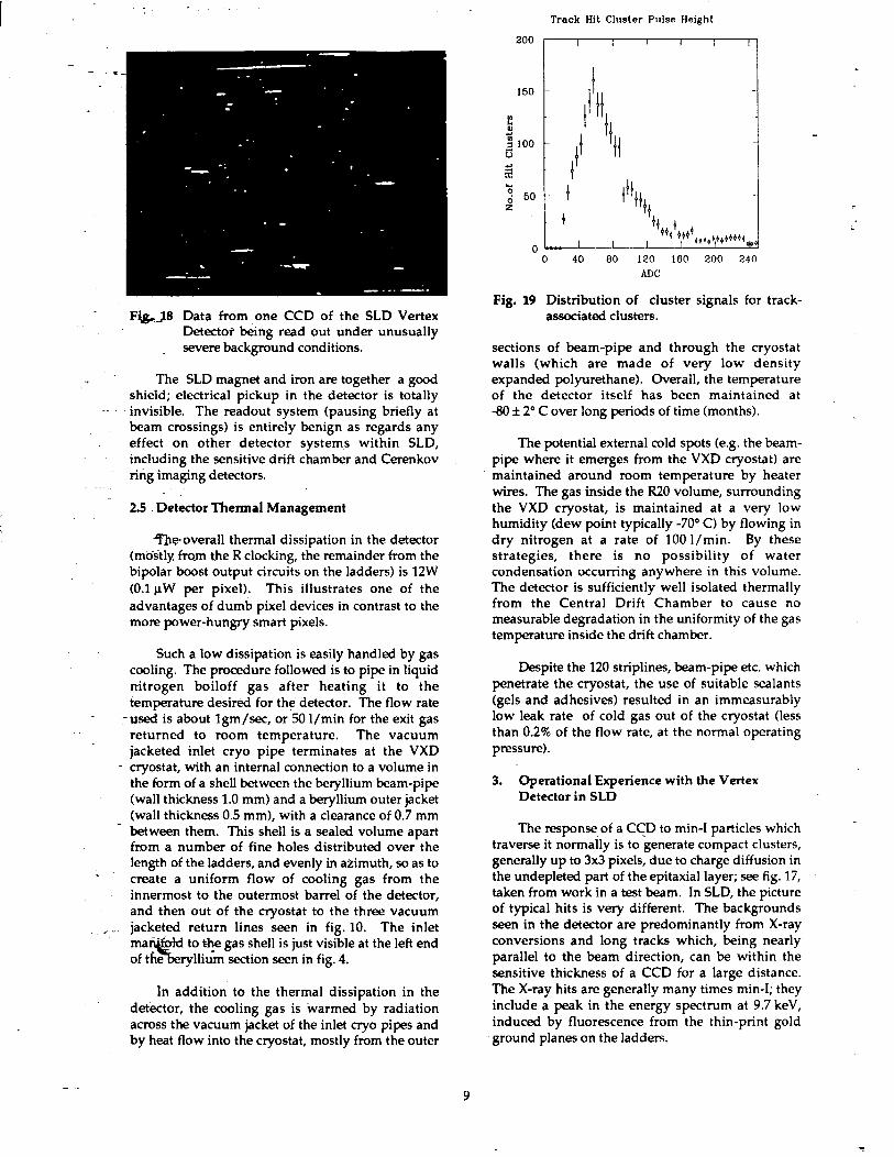
Track Hit Cluster Pulse Height
F&J8 Data from one CCD of the SLD Vertex Detector being read out under unusually
_ severe background conditions.
The SLD magnet and iron are together a good shield; electrical pickup in the detector is totally invisible. The readout system (pausing briefly at beam crossings) is entirely benign as regards any effect on other detector system? within SLD, including the sensitive drift chamber and Cerenkov ring imaging detectors.
i
2.5 Detector Thermal Management
Qe-overall thermal dissipation in the detector (mditly fro-m the R clocking, the remainder from the bipolar boost output circuits on the ladders) is 12W (0.1 PW per pixel). This illustrates one of the advantages of dumb pixel devices in contrast to the more power-hungry smart pixels.
Such a low dissipation is easily handled by gas cooling. The procedure followed is to pipe in liquid nitrogen boiloff gas after heating it to the temperature desir(td for the detector. The flow rate used is about lgm/sec, or 50 l/min for the exit gas returned to room temperature. The vacuum jacketed inlet cryo pipe terminates at the VXD cryostat, with an internal connection to a volume in the form of a shell between the beryllium beam-pipe (wall thickness 1.0 mm) and a beryllium outer jacket (wall thickness 0.5 mm), with a clearance of 0.7 mm between them. This shell is a sealed volume apart from a number of fine holes distributed over the length of the ladders, and evenly in aiimuth, so as to create a uniform flow of cooling gas from the innermost to the outermost barrel of the detector, and then out of the cryostat to the three vacuum jacketed return lines seen in fig. 10. The inlet ma .~‘.f&ld to +e gas shell is just visible at the left end of the %e ryllium section seen in fig. 4.
In addition to the thermal dissipation in the detector, the cooling gas is warmed by radiation across the vacuum jacket of the inlet cryo pipes and by heat flow into the cryostat, mostly from the outer
150
n - 0 40 80 120 180 200 240
ADC
Fig. 19 Distribution of cluster signals for track- associated clusters.
sections of beam-pipe and through the cryostat walls (which are made of very low density expanded polyurethane). Overall, the temperature of the detector itself has been maintained at -80 It 2” C over long periods of time (months).
The potential external cold spots (e.g. the beam- pipe where it emerges from the VXD cryostat) are maintained around room temperature by heater wires. The gas inside the R20 volume, surrounding the VXD cryostat, is maintained at a very low humidity (dew point typically -70” C) by flowing in dry nitrogen at a rate of 100 l/min. By these strategies, there is no possibility of water condensation occurring anywhere in this volume. The detector is sufficiently well isolated thermally from the Central Drift Chamber to cause no measurable degradation in the uniformity of the gas temperature inside the drift chamber.
Despite the 120 striplines, beam-pipe etc. which penetrate the cryostat, the use of suitable sealants (gels and adhesives) resulted in an immeasurably low leak rate of cold gas out of the cryostat (less than 0.2% of the flow rate, at the normal operating pressure).
3. Operational Experience with the Vertex Detector in SLD
The response of a CSD to min-1 particles which traverse it normally is to generate compact clusters, generally up to 3x3 pixels, due to charge diffusion in the undepleted part of the epitaxial layer; see fig. 17, taken from work in a test beam. In SLD, the picture of typical hits is very different. The backgrounds seen in the detector are predominantly from X-ray conversions and long tracks which, being nearly parallel to the beam direction, can be within the sensitive thickness of a CCD for a large distance. The X-ray hits are generally many times min-1; they include a peak in the energy spectrum at 9.7 keV, induced by fluorescence from the thin-print gold ground planes on the ladders.
9

0
Triplet Hit x-y Residual
40
H ‘i;
. 20 z I
Triplet Hit z Residual
I ’ I r I ’ I 1 I
oU -40 -20 0 20 40
m-n
Fig. 20 Detector tracking precision, illustrated by triplet residuals In the XY and RZ planes, with Gaussian fits to
-.. e4 the distributions.
The background at the interaction region of SLC is the most sensitive indicator of the state of operation of the machine. It fluctuates due to innumerable factors; fig. 18 shows data from one of the CCDs under severe conditions, in which it would not have been possible to turn on the drift chamber high voltage. Even under these conditions,
_~ the fine granularity of the Vertex Detector allows one io distinguish clearly the interactions taking pl&,- with negligible overlap. The long tracks result frism e@trons travelling almost parallel to the main-beam, after- scattering off remote collimators, while theX-rays result from synchrotron radiation hitting close-in masks. Both background sources change independently of one another as SLC is tuned. The Vertex Detector is both a valuable diagnostic tool for understanding background, and a robust detector which can be used under conditions where gaseous detectors must be switched off. Background conditions are typically a factor of two higher on the innermost VXD barrel compared with the outermost. i-
The observed background is the accumulation from 19 beam crossings. A microstrip detector read ,_yc. s.eD.l. .y n ,
out promptly would in this respect be 19 times cleaner. However, the SLD Vertex Detector has a granularity which is about 2300 times finer than a corresponding strip detector (‘strip lengths’ typically 50 mm in one case, 22 pm in the other). Thus overall, the occupancy in the pixel based vertex detector is 120 times less than for a strip detector. Furthermore, being 15 times thinner than a microstrip detector, the background in the CCD detector is correspondingly reduced. Overall, one obtains clean signals from the pixel detector under conditions in which microstrip detectors would be saturated.
4. Event Reconstruction
Above-threshold pixel signals written to tape are used offline to reconstitute the clusters of which they form a part. Clusters from min-1 particles are compact, whereas those from various background processes may cover many pixels (as seen in fig. 18). Offline, the position of the cluster centroid is determined, as well as the overall signal charge in the cluster. For very small signals, it frequently happens that only one pixel is above threshold, and yeta large part (maybe 50%) of the cluster signal ,-, , ~ ,e”*c. nyl S.l. PII 0 ( . .
2’
40 60 mm
Fig. 21 XY View of a reconlitructed event as seen in the VXD region of SLD. Drift Chamber tracks alone (left) and Drift Chamber plus VXD combined fit (right).
10

Fig. 22 RZ view. Otherwise as Fig. 21. Drift Chamber alone (left) and Drift Chamber plus VXD (right).
mcy be in surrounding pixels, which are below threshold. To avoid seriously underestimating the cluster signal, the 68020 outputs the 3x3 cluster signal as well as the pixel signal, in such cases. In this way the offline cluster signal is guaranteed to be reasonably complete in small-signal cases. This is particularly important since a threshold cut is imposed offline on the signal charge, so as to fine tune the background rejection in the analysis.
_ _~ Reconstructed drift chamber tracks, which satis& a number of selection criteria designed to provide a reliable sample, are used for linking to hits in thq Vertex Detector. The general procedure is to define. a-primary search area (based on a fairly coarse road) in one of the VXD barrels, and to use hits found within this ares as a basis for a trial track fit. Extrapolating the track through one of these hits to other barrels allows one to impose a much tighter secondary search area. Requiring two or more hits in the VXD to be associated with a linked track gives high linking efficiency and low accidental background. Detailed values for these quantities will emerge as the tuning of the event reconstruction
.-- code is completed. Already, a fairly convincing indication that the detector efficiency is very high
0 2 4 6 810
/// ,,i’ mm
2’
can be seen in fig. 19, which shows the cluster signals for track-associated clusters, subject to a software cut of 20 ADC counts. The broadened Landau distribution, typical of very thin silicon detectors, is in at least qualitative agreement with previous experiments and theory 1121.
The tracking spatial precision on a ladder can be deduced from tracks which traverse the overlap region between CCDs on opposite sides of the same ladder. The procedure is to look at socalled triplet tracks, where we see two hits on one ladder and at least one other track-associated hit on another ladder. A helix fit is made to the track using only the outer two hits of the triplet. In Fig. 20 rye plot the residuals in the XY and RZ planes between the inner hit of the three and this fitted track. The widths of the distributions are 42 times the single- CCD tracking precision, plus any additional effects due to survey errors in the positions of CCDs on opposite sides of a ladder. Assuming that the survey errors are negligible, the fits to these residual distributions imply individual CCD tracking precision of 5.0 pm in the XY plane and 7.8 ~UII in the RZ plane. Since the detector internal geometry is defined purely from the optical survey at this stage,
0 2 4 6 8 10 mm
Fig. 23 As Fig. 21, but on an expanded scale. The VXD+CDC reconstruction (right) indicates a possible secondary decay vertex with a projected flight path of approximately 15 mm.
-- 11

further improvements may still be possible after alignment corrections with tracks. Note also that
- 9 --the RZ plots include tracks tilted down to polar angles of 400, where several factors could in principle degrade the measurement precision. _
The application of the Vertex Detector to the recognition of heavy flavour decays is now beginning. As an example event, fig. 21 shows in the XY view the benefit obtained by using the VXD hits in a combined fit with the CDC. Since the CCD-based detector measures space points, we can rotate the event and look at the vertex region with similar precision from any direction. Fig. 22 shows the RZ view (the view in the event plane including the Z axis). Here the drift chamber tracks are less well measured due to the small stereo angle of the chsmber wires, but again the inclusion of the VXD hits produces -a much improved precision of reconstruction. In Fig. 23, we look again at the XY view- for the same event, on an expanded scale. Some of the tracks in the 8 to 9 o’clock region indicate the presence of a secondary decay vertex; one isolated track (number 1) may even indicate a tertiary decay vertex.
R Bailey, C J S Damerell, R L English, A R Gillman, A L Lintern, S J Watts and F J Wickens
Conclusions Nud. Inst. and Meth. 213 (1983) 201.
_~ This project has firstly demonstrated the feasibility of building a large mosaic of CCDs and operating it in an essentially inaccessible env+uunent, with excellent reliability. This reflects on the.enqrmous steps which have been taken in the quality control of CCD manufacture in recent years.
Secondly, we have demonstrated the feasibility of constructing a complex mechanical assembly which can be surveyed optically in stages (with necessarily d&assembly and m-assembly between stages) with a final internal precision at the 5 Pm level.
.-. Thirdly, we have made the transition for pixel- based vertex detectors from the fixed-target environment with two CCDs to the collider
- environment with 480 CCDs (small to large solid angle coverage) and demonstrated the potential for doing heavy flavour physics in the collider environment.
Finally, we have shown that a large CCD system of this type (120 Mpixels) can be read out with low noise, and that the data sparsification allows full detector readout even under severe background conditions. The deadtimeless character
, _. of the readout is important. The relatively slow readout does create increased background in the de&&or, but-this is more than compensated by the high degree of granularity, which probably exceeds that of any electronic detector previousl,y used in high energy physics. The data are in this respect more similar to those provided by nuclear emulsions.
Acknowledgements
This lengthy project has benefited from the help of many individuals who are not on the author list. We wish especially to thank Marty Breidenbach, Richard Claus, John Fox, James Russell and - Leo Paffrath (SLAC), David Burt, Gerry Swallow and Robert Millea (Hirst Research Centre), John Ashton and Peter Pool (EEV). All of these provided valuable advice and guidance. The technical support of Lester Harwood (SLAC) is also gratefully acknowledged. JR thanks the Sloan Foundation and the DOE OJI program (grant DE- FGO3-91ER-40618, Task K). MGS acknowledges the support of DOE grant DE-FGO2-92ER40715.
REFERENCES
1
2
3
4
5
6
7
8
9
10
11
12
C J S Damerell, F J M Farley, A R Gillman and F J Wickens Nud. Inst. and Mefh. 185 (1981) 33.
S Barlag et al (ACCMOR Collaboration). Phys. I.&. 184B (1987) 283.
S Barlag et al (ACCMOR Collaboration1 Phys. Lett. 236B (1990) 495.
C J S Damerell, R L English, A R Gillman, A L Lintern, F J Wickens, G Agnew and S J Watts Nud. Inst. and Meth. A253 (1987) 478.
CCDs used for this detector were UT101 devices from the EEV Company, Chelmsford, Essex, England.
I-400 Material was obtained from Brush Wellman Inc., Cleveland, Ohio, USA. Machining was by Loral American Beryllium, Tallevast, Florida, USA.
The adhesive used was CV-1142 of McGhan Nusil Corp., Carpinteria, California, USA.
D A Phillips and A R Gillman, Rutherford Appzefon tiorafory Preprzrlt RAL-89064 (1989).
C J S Damerell, A R Gillman and D A Phillips, IEEE Runs Nud. Sci 37 (1990) 305.
J D Fox et al, Nucl. Phys B, Pm. Suppl. (Nefhdands) 23A (1991) 227.
H Bichsel, Revs Mod Physics 60 (19881663.
12