Embed Size (px)
Citation preview
HAL Id: hal-01383727https://hal.inria.fr/hal-01383727
Submitted on 19 Oct 2016
HAL is a multi-disciplinary open accessarchive for the deposit and dissemination of sci-entific research documents, whether they are pub-lished or not. The documents may come fromteaching and research institutions in France orabroad, or from public or private research centers.
L’archive ouverte pluridisciplinaire HAL, estdestinée au dépôt et à la diffusion de documentsscientifiques de niveau recherche, publiés ou non,émanant des établissements d’enseignement et derecherche français ou étrangers, des laboratoirespublics ou privés.
Distributed under a Creative Commons Attribution| 4.0 International License
Design and Optimization of Multiple-Mesh ClockNetwork
Jinwook Jung, Dongsoo Lee, Youngsoo Shin
To cite this version:Jinwook Jung, Dongsoo Lee, Youngsoo Shin. Design and Optimization of Multiple-Mesh Clock Net-work. 22th IFIP/IEEE International Conference on Very Large Scale Integration - System on a Chip(VLSI-SoC 2014), Oct 2014, Playa del Carmen, Mexico. pp.39-57, �10.1007/978-3-319-25279-7_3�.�hal-01383727�
Design and Optimization of Multiple-MeshClock Network
Jinwook Jung, Dongsoo Lee, and Youngsoo Shin
Korea Advanced Institute of Science and Technology291 Daehak-ro, Yuseong-gu, Daejeon 305-701, Korea,
Abstract. A clock mesh, in which clock signals are shorted at meshgrid, is less susceptible to on-chip process variation, and so it has widelybeen studied recently for a clock network of smaller skew. A practicaldesign may require more than one mesh primarily because of hierarchicalclock gating architecture; a single mesh, however, can also support thesame architecture after some hierarchies are removed but at the cost ofgating efficiency. We experimentally compare multiple- and single-meshusing a few test circuits, and show that the former consumes smallerclock power (16.3%) but exhibits larger clock skew (10.2ps) and longerclock wirelength (21.7%). We continue to study how multiple meshesshould be floorplanned on the layout, specifically whether or not we al-low the overlaps among meshes. The choice is translated into differentphysical design strategy, and causes different amount of clock skew, crit-ical path delay, clock wirelength, and clock power consumption, whichwe experimentally evaluate. We give at last the comparison of clock skewvariation for each mesh implementation and clock tree, and show thatfloorplanning of multiple meshes helps to reduce the variation of clockskew.
Keywords: Clock distribution, Clock mesh, Multiple-mesh clock net-work
1 Introduction
Big industrial designs such as SoCs and processors are often embedded withmultiple levels of clock gating to efficiently reduce the power consumption ofclock distribution network [1–3]. Some clock gating is inserted by automaticCAD tools, e.g. by compiling load-enable registers into normal registers drivenby clock gating cells (CGCs); designers may also insert clock gating in manualfashion, especially at module- or system-level, based on the knowledge of theusage scenario of a design [4].
If the clock network of such a design is to be constructed using clock meshesto achieve lower clock skew, multiple meshes may be inserted as shown in Fig. 1.This is a natural choice in terms of power consumption because each mesh canbe gated whenever the block it spans is not actively switching. Furthermore, it is
II
Multiple meshes
Mesh 1
Mesh 2
Non-overlapping meshes
Mesh 2Mesh 1
Overlapping meshes
Mesh 2Mesh 1
Multi-levelclock gating
CGC FF
Mesh
Single mesh
Mesh
Fig. 1: Design of mesh clock network for multi-level clock gating.
well known that mesh consumes more power than standard clock tree network [5]due to more wire capacitance and excessive short-circuit current; a study indi-cates that 33.4% more power is consumed in comparison with the standard clocktree [6], so it helps to gate mesh whenever it is possible. A single big mesh, how-ever, may be inserted instead after some clock gating hierarchies are removed,which is also illustrated in Fig. 1. This choice is not efficient in terms of powerconsumption, but it has the benefits of shorter design time because of its simplerstructure, as well as shorter clock wires and more importantly smaller clock skew.In this paper, we quantitatively explore the two styles of mesh implementation,using some test circuits in 28-nm technology, which is the first contribution.
When multiple meshes are employed, it is important to decide how to floor-plan them. If overlaps between meshes are allowed, physical design can be donein flat. No overlap, on the other hand, implies hierarchical physical design. Thetwo styles will have different impact on clock power, clock wirelength, clock skew,and timing closure, which we want to quantitatively assess; this constitutes thesecond contribution of the paper.
III
Premesh tree
Clock mesh
Postmesh tree
Mesh drivers
Postmesh buffers
Clock sinks
Stub wires
Fig. 2: Mesh clock network.
The remainder of this paper is organized as follows. The basic mesh networkstructure and the steps to synthesize it are reviewed in Section 2; clock gatingin multiple levels of hierarchy is also described. In Section 3, we address theprocedures to design single- and multiple-mesh clock networks in the context ofmulti-level clock gating, and use some test circuits to experimentally assess thetwo implementation styles. Section 5 discusses the floorplan of multiple meshesand provides experimental evaluation. Section 6 gives the comparison of thethree mesh implementations with the standard clock tree, and evaluates clockskew variation. Several related works are reviewed in Section 7, and we finallyconclude the paper in Section 8.
2 Preliminaries
2.1 Clock Mesh Structure and Its Synthesis
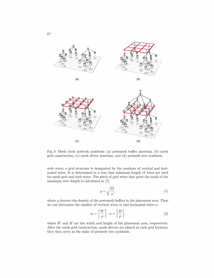
Fig. 2 illustrates a structure of mesh clock network that we are concerned within this paper. It consists of three main components: a premesh tree, a mesh grid,and a postmesh tree. Clock sinks are connected to the mesh through postmeshbuffers and stub wires. A premesh tree can be a balanced H-tree or standardclock tree, and connects the mesh to the clock source. Leaf-stage buffers in thepremesh tree will be called mesh drivers.
Fig. 3 illustrates the overall synthesis flow of a mesh clock network; we synthe-size a mesh clock network in a bottom-up manner. Clock sinks are first groupedtogether based on their locations; maximum fanout of postmesh buffers, whichare inserted and sized properly once the groups are formed, determines the groupsize. A mesh grid is constructed and connected to the postmesh buffers through
IV
(a) (b)
(d)(c)
Fig. 3: Mesh clock network synthesis: (a) postmesh buffer insertion, (b) meshgrid construction, (c) mesh driver insertion, and (d) premesh tree synthesis.
stub wires; a grid structure is designated by the numbers of vertical and hori-zontal wires. It is determined in a way that minimum length of wires are usedfor mesh grid and stub wires. The pitch of grid wires that gives the mesh of theminimum wire length is calculated as [7]:
p =√
12ρ, (1)
where ρ denotes the density of the postmesh buffers in the placement area. Thenwe can determine the number of vertical wires m and horizontal wires n:
m =⌈W
p
⌉, n =
⌈H
p
⌉, (2)
where W and H are the width and height of the placement area, respectively.After the mesh grid construction, mesh drivers are placed at each grid location;they then serve as the sinks of premesh tree synthesis.
V
Module-level clock gating Register-levelclock gating
Module 1 Module 2 Module 3
System-level clock gating
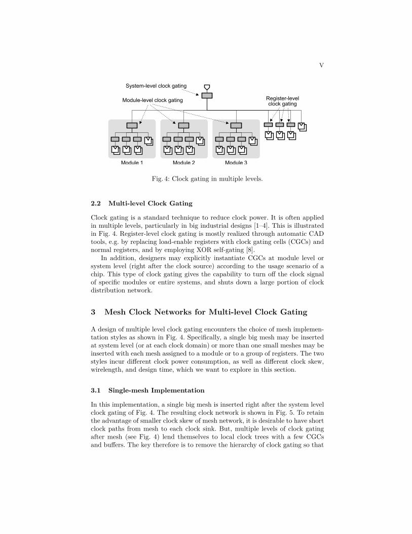
Fig. 4: Clock gating in multiple levels.
2.2 Multi-level Clock Gating
Clock gating is a standard technique to reduce clock power. It is often appliedin multiple levels, particularly in big industrial designs [1–4]. This is illustratedin Fig. 4. Register-level clock gating is mostly realized through automatic CADtools, e.g. by replacing load-enable registers with clock gating cells (CGCs) andnormal registers, and by employing XOR self-gating [8].
In addition, designers may explicitly instantiate CGCs at module level orsystem level (right after the clock source) according to the usage scenario of achip. This type of clock gating gives the capability to turn off the clock signalof specific modules or entire systems, and shuts down a large portion of clockdistribution network.
3 Mesh Clock Networks for Multi-level Clock Gating
A design of multiple level clock gating encounters the choice of mesh implemen-tation styles as shown in Fig. 4. Specifically, a single big mesh may be insertedat system level (or at each clock domain) or more than one small meshes may beinserted with each mesh assigned to a module or to a group of registers. The twostyles incur different clock power consumption, as well as different clock skew,wirelength, and design time, which we want to explore in this section.
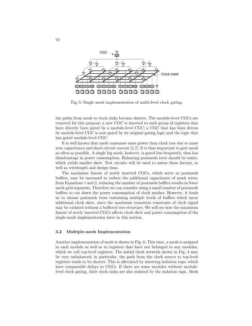
3.1 Single-mesh Implementation
In this implementation, a single big mesh is inserted right after the system levelclock gating of Fig. 4. The resulting clock network is shown in Fig. 5. To retainthe advantage of smaller clock skew of mesh network, it is desirable to have shortclock paths from mesh to each clock sink. But, multiple levels of clock gatingafter mesh (see Fig. 4) lend themselves to local clock trees with a few CGCsand buffers. The key therefore is to remove the hierarchy of clock gating so that
VI
Clock mesh
CGC
Fig. 5: Single mesh implementation of multi-level clock gating.
the paths from mesh to clock sinks become shorter. The module-level CGCs areremoved for this purpose; a new CGC is inserted to each group of registers thathave directly been gated by a module-level CGC; a CGC that has been drivenby module-level CGC is now gated by its original gating logic and the logic thathas gated module-level CGC.
It is well known that mesh consumes more power than clock tree due to morewire capacitance and short-circuit current [5,7]. It is thus important to gate meshas often as possible. A single big mesh, however, is gated less frequently, thus hasdisadvantage in power consumption. Balancing postmesh trees should be easier,which yields smaller skew. Test circuits will be used to assess these factors, aswell as wirelength and design time.
The maximum fanout of newly inserted CGCs, which serve as postmeshbuffers, may be increased to reduce the additional capacitance of mesh wires;from Equations 1 and 2, reducing the number of postmesh buffers results in fewermesh grid segments. Therefore we can consider using a small number of postmeshbuffers to cut down the power consumption of clock meshes. However, it leadsus to choose postmesh trees containing multiple levels of buffers which incuradditional clock skew, since the maximum transition constraint of clock signalmay be violated without a buffered tree structure. We will see how the maximumfanout of newly inserted CGCs affects clock skew and power consumption of thesingle-mesh implementation later in this section.
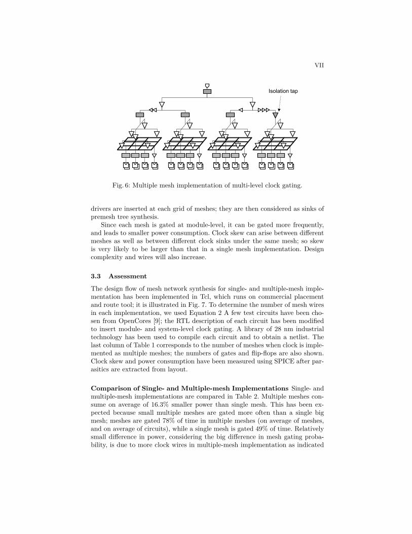
3.2 Multiple-mesh Implementation
Another implementation of mesh is shown in Fig. 6. This time, a mesh is assignedto each module as well as to registers that have not belonged to any modules,which we call top-level registers. The initial clock network shown in Fig. 4 maybe very unbalanced; in particular, the path from the clock source to top-levelregisters tends to be shorter. This is alleviated by inserting isolation taps, whichhave comparable delays to CGCs. If there are some modules without module-level clock gating, their clock sinks are also isolated by the isolation taps. Mesh
VII
Isolation tap
Fig. 6: Multiple mesh implementation of multi-level clock gating.
drivers are inserted at each grid of meshes; they are then considered as sinks ofpremesh tree synthesis.
Since each mesh is gated at module-level, it can be gated more frequently,and leads to smaller power consumption. Clock skew can arise between differentmeshes as well as between different clock sinks under the same mesh; so skewis very likely to be larger than that in a single mesh implementation. Designcomplexity and wires will also increase.
3.3 Assessment
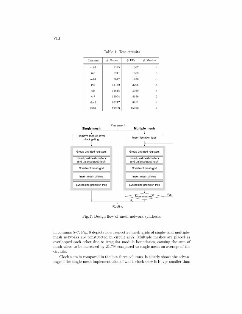
The design flow of mesh network synthesis for single- and multiple-mesh imple-mentation has been implemented in Tcl, which runs on commercial placementand route tool; it is illustrated in Fig. 7. To determine the number of mesh wiresin each implementation, we used Equation 2 A few test circuits have been cho-sen from OpenCores [9]; the RTL description of each circuit has been modifiedto insert module- and system-level clock gating. A library of 28 nm industrialtechnology has been used to compile each circuit and to obtain a netlist. Thelast column of Table 1 corresponds to the number of meshes when clock is imple-mented as multiple meshes; the numbers of gates and flip-flops are also shown.Clock skew and power consumption have been measured using SPICE after par-asitics are extracted from layout.
Comparison of Single- and Multiple-mesh Implementations Single- andmultiple-mesh implementations are compared in Table 2. Multiple meshes con-sume on average of 16.3% smaller power than single mesh. This has been ex-pected because small multiple meshes are gated more often than a single bigmesh; meshes are gated 78% of time in multiple meshes (on average of meshes,and on average of circuits), while a single mesh is gated 49% of time. Relativelysmall difference in power, considering the big difference in mesh gating proba-bility, is due to more clock wires in multiple-mesh implementation as indicated
VIII
Table 1: Test circuits
Circuits # Gates # FFs # Meshes
ac97 3225 1067 4
mc 6211 1069 3
usbf 7647 1736 3
pci 11142 3206 4
sdc 11815 3760 5
spi 13964 4656 2
des3 63217 8811 4
fft64 71263 15996 4
Placement
Routing
Multiple mesh
GroupNungated registersN
InsertNpostmesh buffersandNbalanceNpostmesh
ConstructNmeshNgrid
InsertNmeshNdrivers
SynthesizeNpremesh tree
MoreNmeshes?Yes
No
InsertNisolationNtaps
Single mesh
GroupNungated registersN
InsertNpostmesh buffersandNbalanceNpostmesh
ConstructNmeshNgrid
InsertNmeshNdrivers
SynthesizeNpremesh tree
RemoveNmodule-levelNclockNgating
Fig. 7: Design flow of mesh network synthesis.
in columns 5–7. Fig. 8 depicts how respective mesh grids of single- and multiple-mesh networks are constructed in circuit ac97. Multiple meshes are placed asoverlapped each other due to irregular module boundaries, causing the sum ofmesh wires to be increased by 21.7% compared to single mesh on average of thecircuits.
Clock skew is compared in the last three columns. It clearly shows the advan-tage of the single-mesh implementation of which clock skew is 10.2ps smaller than
IX
Table 2: Comparison of single- and multiple-mesh implementation
Clock power (mW) Clock wirelength (mm) Clock skew (ps)
Circuits Single Multiple Diff. (%) Single Multiple Diff. (%) Single Multiple Diff. (ps)
ac97 0.52 0.43 17.1 5.5 6.6 -20.0 13.5 26.6 -13.1
mc 0.18 0.15 18.2 4.8 6.3 -31.7 13.4 20.9 -7.5
usbf 0.89 0.85 10.0 7.6 10.0 -31.8 11.8 27.0 -15.2
pci 0.50 0.45 11.8 13.9 17.8 -28.7 13.4 26.1 -12.7
sdc 0.45 0.32 28.2 14.3 17.6 -23.6 14.0 23.3 -9.3
spi 0.84 0.62 26.1 18.3 20.2 -10.8 12.5 19.6 -7.0
des3 2.95 2.55 13.6 38.2 45.5 -19.4 14.0 24.5 -10.5
fft64 1.74 1.55 10.9 62.6 67.7 -8.0 19.8 26.0 -6.2
Average 16.3 -21.7 -10.2
(a) (b)
Fig. 8: Layouts of (a) single- and (b) multiple-mesh implementations for circuitac97.
that of the multiple meshes on average, which also has been expected. Postmeshbuffers are close to a mesh grid in the single-mesh while the stub wires of themultiple-mesh implementations becomes longer (see Fig. 8 (b)), which introduceadditional clock skew due to the stub wire delay. Also, different meshes them-selves contribute to clock skew in the multiple-mesh implementation due to thedifferent latenciy from the clock source to each mesh (see Fig. 6).
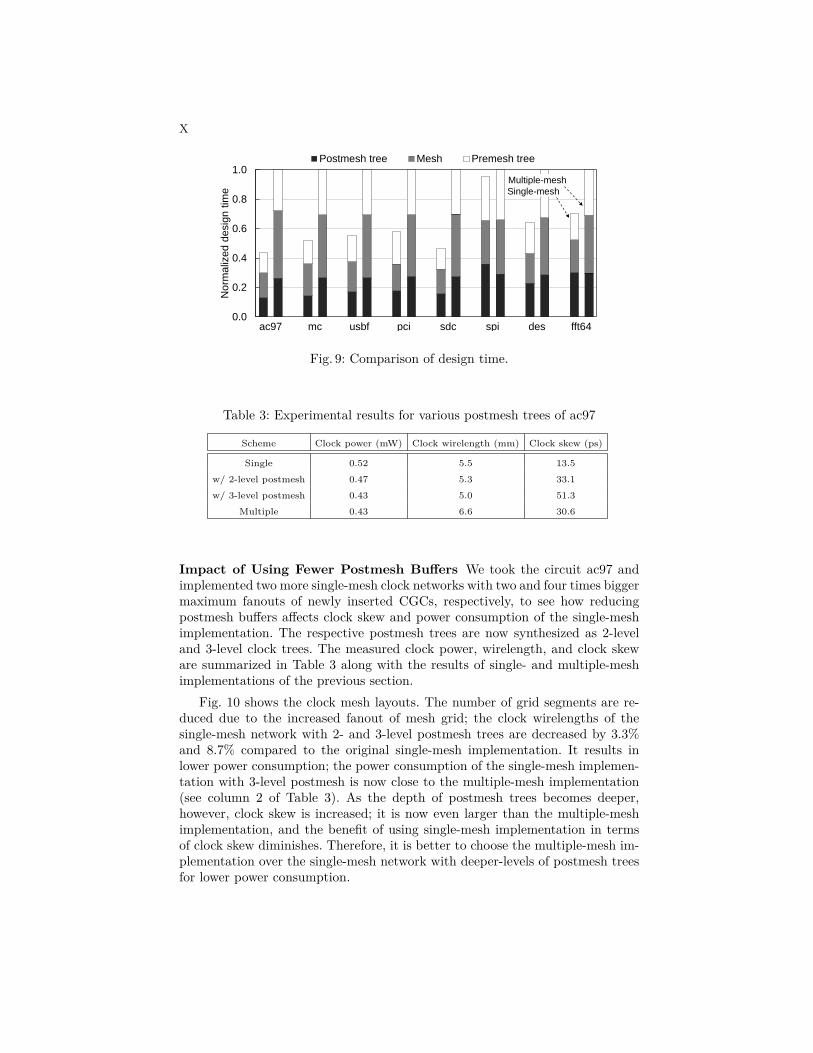
Fig. 9 compares the time elapsed for clock network synthesis. Multiple-meshimplementation takes 35.4% more time than single-mesh, on average. This ismainly due to the fact that designing mesh grid and postmesh trees has to beiterated in the multiple-mesh implementation. A circuit spi is an exception. Itcontains only two meshes in its multiple-mesh implementation; more times arespent in the postmesh tree synthesis of single-mesh implementation due to thelarge number of clock sinks (in consideration of circuit size).
X
0.0
0.2
0.4
0.6
0.8
1.0
Norm
aliz
ed d
esig
n t
ime
Postmesh tree Mesh Premesh tree
ac97 usbf pci des fft64mc sdc spi
Multiple-mesh
Single-mesh
Fig. 9: Comparison of design time.
Table 3: Experimental results for various postmesh trees of ac97
Scheme Clock power (mW) Clock wirelength (mm) Clock skew (ps)
Single 0.52 5.5 13.5
w/ 2-level postmesh 0.47 5.3 33.1
w/ 3-level postmesh 0.43 5.0 51.3
Multiple 0.43 6.6 30.6
Impact of Using Fewer Postmesh Buffers We took the circuit ac97 andimplemented two more single-mesh clock networks with two and four times biggermaximum fanouts of newly inserted CGCs, respectively, to see how reducingpostmesh buffers affects clock skew and power consumption of the single-meshimplementation. The respective postmesh trees are now synthesized as 2-leveland 3-level clock trees. The measured clock power, wirelength, and clock skeware summarized in Table 3 along with the results of single- and multiple-meshimplementations of the previous section.
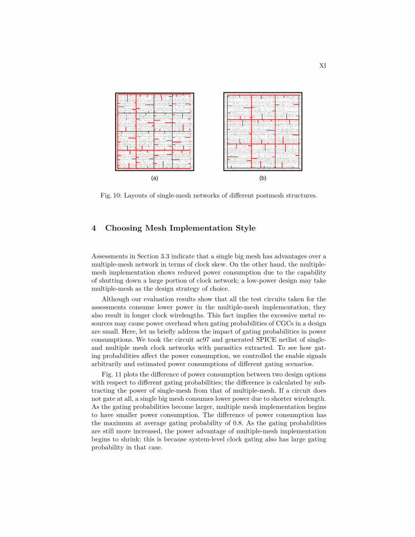
Fig. 10 shows the clock mesh layouts. The number of grid segments are re-duced due to the increased fanout of mesh grid; the clock wirelengths of thesingle-mesh network with 2- and 3-level postmesh trees are decreased by 3.3%and 8.7% compared to the original single-mesh implementation. It results inlower power consumption; the power consumption of the single-mesh implemen-tation with 3-level postmesh is now close to the multiple-mesh implementation(see column 2 of Table 3). As the depth of postmesh trees becomes deeper,however, clock skew is increased; it is now even larger than the multiple-meshimplementation, and the benefit of using single-mesh implementation in termsof clock skew diminishes. Therefore, it is better to choose the multiple-mesh im-plementation over the single-mesh network with deeper-levels of postmesh treesfor lower power consumption.
XI
(a) (b)
Fig. 10: Layouts of single-mesh networks of different postmesh structures.
4 Choosing Mesh Implementation Style
Assessments in Section 3.3 indicate that a single big mesh has advantages over amultiple-mesh network in terms of clock skew. On the other hand, the multiple-mesh implementation shows reduced power consumption due to the capabilityof shutting down a large portion of clock network; a low-power design may takemultiple-mesh as the design strategy of choice.
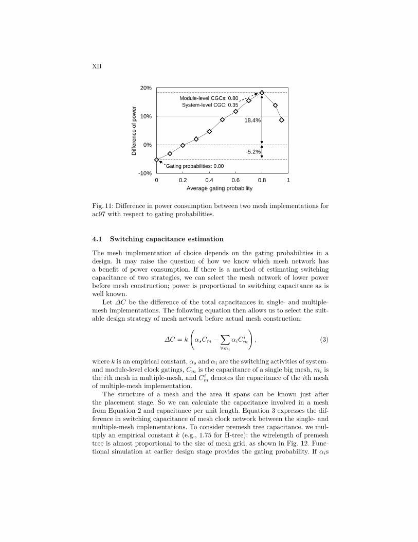
Although our evaluation results show that all the test circuits taken for theassessments consume lower power in the multiple-mesh implementation, theyalso result in longer clock wirelengths. This fact implies the excessive metal re-sources may cause power overhead when gating probabilities of CGCs in a designare small. Here, let us briefly address the impact of gating probabilities in powerconsumptions. We took the circuit ac97 and generated SPICE netlist of single-and multiple mesh clock networks with parasitics extracted. To see how gat-ing probabilities affect the power consumption, we controlled the enable signalsarbitrarily and estimated power consumptions of different gating scenarios.
Fig. 11 plots the difference of power consumption between two design optionswith respect to different gating probabilities; the difference is calculated by sub-tracting the power of single-mesh from that of multiple-mesh. If a circuit doesnot gate at all, a single big mesh consumes lower power due to shorter wirelength.As the gating probabilities become larger, multiple mesh implementation beginsto have smaller power consumption. The difference of power consumption hasthe maximum at average gating probability of 0.8. As the gating probabilitiesare still more increased, the power advantage of multiple-mesh implementationbegins to shrink; this is because system-level clock gating also has large gatingprobability in that case.
XII
-10%
0%
10%
20%
0 0.2 0.4 0.6 0.8 1
Diffe
ren
ce
of p
ow
er
Average gating probability
Gating probabilities: 0.00
18.4%
-5.2%
Module-level CGCs:
System-level CGC:
0.80
0.35
Fig. 11: Difference in power consumption between two mesh implementations forac97 with respect to gating probabilities.
4.1 Switching capacitance estimation
The mesh implementation of choice depends on the gating probabilities in adesign. It may raise the question of how we know which mesh network hasa benefit of power consumption. If there is a method of estimating switchingcapacitance of two strategies, we can select the mesh network of lower powerbefore mesh construction; power is proportional to switching capacitance as iswell known.
Let ∆C be the difference of the total capacitances in single- and multiple-mesh implementations. The following equation then allows us to select the suit-able design strategy of mesh network before actual mesh construction:
∆C = k
(αsCm −
∑∀mi
αiCim
), (3)
where k is an empirical constant, αs and αi are the switching activities of system-and module-level clock gatings, Cm is the capacitance of a single big mesh, mi isthe ith mesh in multiple-mesh, and Ci
m denotes the capacitance of the ith meshof multiple-mesh implementation.
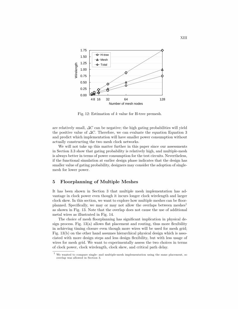
The structure of a mesh and the area it spans can be known just afterthe placement stage. So we can calculate the capacitance involved in a meshfrom Equation 2 and capacitance per unit length. Equation 3 expresses the dif-ference in switching capacitance of mesh clock network between the single- andmultiple-mesh implementations. To consider premesh tree capacitance, we mul-tiply an empirical constant k (e.g., 1.75 for H-tree); the wirelength of premeshtree is almost proportional to the size of mesh grid, as shown in Fig. 12. Func-tional simulation at earlier design stage provides the gating probability. If αis
XIII
0.00
0.25
0.50
0.75
1.00
1.25
1.50
1.75
Wire
len
gth
Number of mesh nodes
H-tree
Mesh
Total
4 8 16 32 64 128
Fig. 12: Estimation of k value for H-tree premesh.
are relatively small, ∆C can be negative; the high gating probabilities will yieldthe positive value of ∆C. Therefore, we can evaluate the equation Equation 3and predict which implementation will have smaller power consumption withoutactually constructing the two mesh clock networks.
We will not take up this matter further in this paper since our assessmentsin Section 3.3 show that gating probability is relatively high, and multiple-meshis always better in terms of power consumption for the test circuits. Nevertheless,if the functional simulation at earlier design phase indicates that the design hassmaller value of gating probability, designers may consider the adoption of single-mesh for lower power.
5 Floorplanning of Multiple Meshes
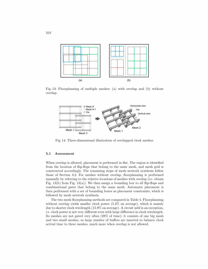
It has been shown in Section 3 that multiple mesh implementation has ad-vantage in clock power even though it incurs longer clock wirelength and largerclock skew. In this section, we want to explore how multiple meshes can be floor-planned. Specifically, we may or may not allow the overlaps between meshes1
as shown in Fig. 13. Note that the overlap does not cause the use of additionalmetal wires as illustrated in Fig. 14.
The choice of mesh floorplanning has significant implication in physical de-sign process. Fig. 13(a) allows flat placement and routing, thus more flexibilityin achieving timing closure even though more wires will be used for mesh grid;Fig. 13(b) on the other hand assumes hierarchical physical design which is asso-ciated with more design steps and less design flexibility, but with less usage ofwires for mesh grid. We want to experimentally assess the two choices in termsof clock power, clock wirelength, clock skew, and critical path delay.1 We wanted to compare single- and multiple-mesh implementation using the same placement, so
overlap was allowed in Section 3.
XIV
(b)(a)
Fig. 13: Floorplanning of multiple meshes: (a) with overlap and (b) withoutoverlap.
Metal NMetal N-1Via
Mesh 1Mesh 2
Mesh 1Mesh 2
Horizontal wire
Via
Vertical wire
Fig. 14: Three-dimensional illustration of overlapped clock meshes.
5.1 Assessment
When overlap is allowed, placement is performed in flat. The region is identifiedfrom the location of flip-flops that belong to the same mesh, and mesh grid isconstructed accordingly. The remaining steps of mesh network synthesis followthose of Section 3.2. For meshes without overlap, floorplanning is performedmanually by referring to the relative locations of meshes with overlap (i.e. obtainFig. 13(b) from Fig. 13(a)). We then assign a bounding box to all flip-flops andcombinational gates that belong to the same mesh. Automatic placement isthen performed with a set of bounding boxes as placement constraints, which isfollowed by mesh network synthesis.
The two mesh floorplanning methods are compared in Table 4. Floorplanningwithout overlap yields smaller clock power (5.2% on average), which is mainlydue to shorter clock wirelength (15.9% on average). A circuit usbf is an exception,i.e. clock power is not very different even with large difference in clock wirelength.Its meshes are not gated very often (28% of time); it consists of one big meshand two small meshes, so large number of buffers are inserted to balance clockarrival time to three meshes, much more when overlap is not allowed.
XV
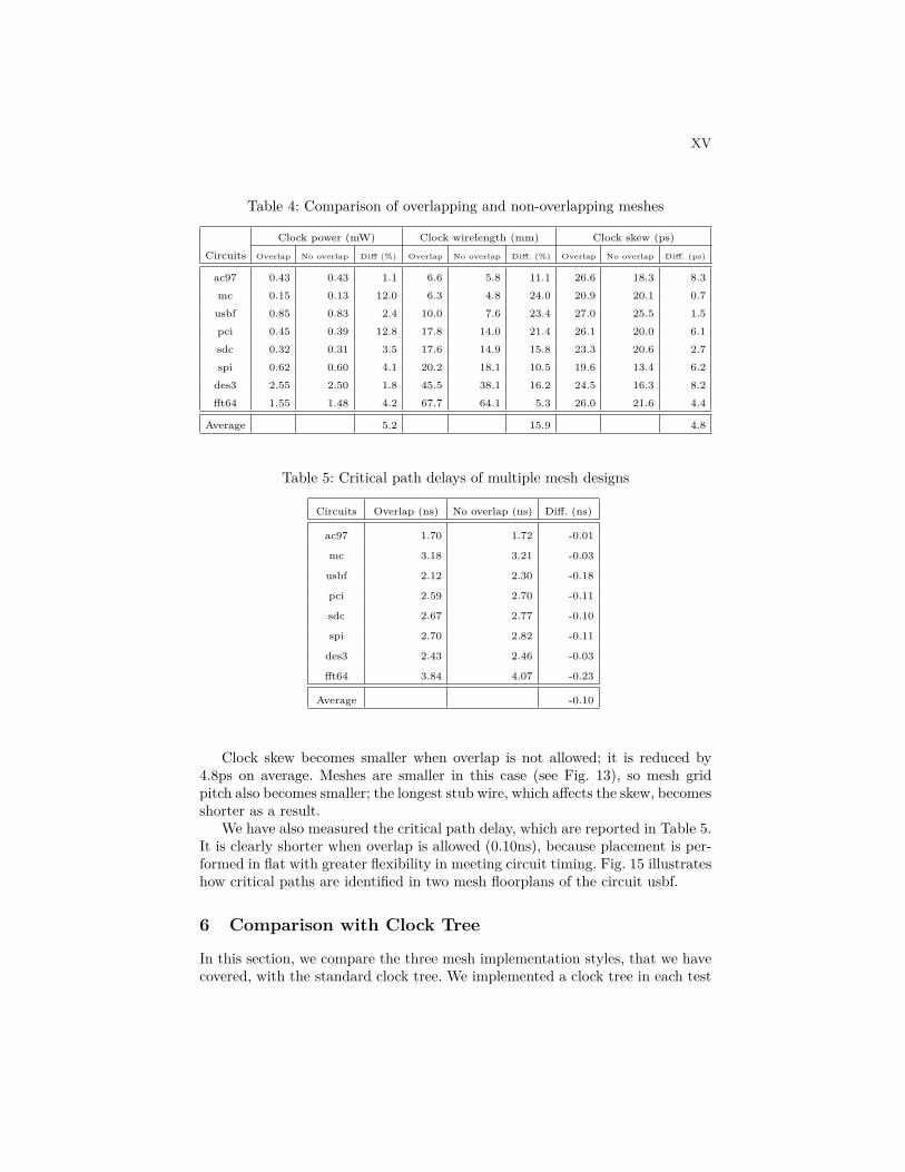
Table 4: Comparison of overlapping and non-overlapping meshes
Clock power (mW) Clock wirelength (mm) Clock skew (ps)
Circuits Overlap No overlap Diff (%) Overlap No overlap Diff. (%) Overlap No overlap Diff. (ps)
ac97 0.43 0.43 1.1 6.6 5.8 11.1 26.6 18.3 8.3
mc 0.15 0.13 12.0 6.3 4.8 24.0 20.9 20.1 0.7
usbf 0.85 0.83 2.4 10.0 7.6 23.4 27.0 25.5 1.5
pci 0.45 0.39 12.8 17.8 14.0 21.4 26.1 20.0 6.1
sdc 0.32 0.31 3.5 17.6 14.9 15.8 23.3 20.6 2.7
spi 0.62 0.60 4.1 20.2 18.1 10.5 19.6 13.4 6.2
des3 2.55 2.50 1.8 45.5 38.1 16.2 24.5 16.3 8.2
fft64 1.55 1.48 4.2 67.7 64.1 5.3 26.0 21.6 4.4
Average 5.2 15.9 4.8
Table 5: Critical path delays of multiple mesh designs
Circuits Overlap (ns) No overlap (ns) Diff. (ns)
ac97 1.70 1.72 -0.01
mc 3.18 3.21 -0.03
usbf 2.12 2.30 -0.18
pci 2.59 2.70 -0.11
sdc 2.67 2.77 -0.10
spi 2.70 2.82 -0.11
des3 2.43 2.46 -0.03
fft64 3.84 4.07 -0.23
Average -0.10
Clock skew becomes smaller when overlap is not allowed; it is reduced by4.8ps on average. Meshes are smaller in this case (see Fig. 13), so mesh gridpitch also becomes smaller; the longest stub wire, which affects the skew, becomesshorter as a result.
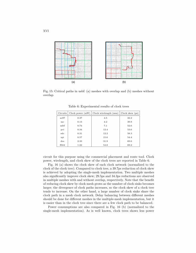
We have also measured the critical path delay, which are reported in Table 5.It is clearly shorter when overlap is allowed (0.10ns), because placement is per-formed in flat with greater flexibility in meeting circuit timing. Fig. 15 illustrateshow critical paths are identified in two mesh floorplans of the circuit usbf.
6 Comparison with Clock Tree
In this section, we compare the three mesh implementation styles, that we havecovered, with the standard clock tree. We implemented a clock tree in each test
XVI
(a) (b)
Fig. 15: Critical paths in usbf: (a) meshes with overlap and (b) meshes withoutoverlap.
Table 6: Experimental results of clock trees
Circuits Clock power (mW) Clock wirelength (mm) Clock skew (ps)
ac97 0.37 4.5 32.2
mc 0.13 4.2 39.9
usbf 0.74 7.1 52.6
pci 0.34 12.4 53.6
sdc 0.31 12.2 58.3
spi 0.57 15.6 54.4
des 2.33 31.9 69.6
fft64 1.22 54.8 69.2
circuit for this purpose using the commercial placement and route tool. Clockpower, wirelength, and clock skew of the clock trees are reported in Table 6.
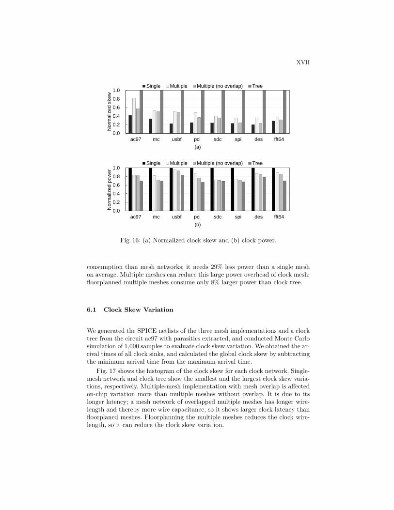
Fig. 16 (a) shows the clock skew of each clock network (normalized to theclock of the clock tree). Compared to clock tree, a 39.7ps reduction of clock skewis achieved by adopting the single-mesh implementation. Two multiple meshesalso significantly improve clock skew; 29.5ps and 34.3ps reductions are observedin multiple meshes with and without overlap, respectively. Note that the benefitof reducing clock skew by clock mesh grows as the number of clock sinks becomeslarger; the divergence of clock paths increases, so the clock skew of a clock treetends to increase. On the other hand, a large number of clock sinks share theclock path in a mesh clock network. Delay balancing between different meshesshould be done for different meshes in the multiple-mesh implementation, but itis easier than in the clock tree since there are a few clock path to be balanced.
Power consumptions are also compared in Fig. 16 (b) (normalized to thesingle-mesh implementation). As is well known, clock trees shows less power
XVII
0.0
0.2
0.4
0.6
0.8
1.0
ac97 mc usbf pci sdc spi des fft64
Norm
aliz
ed s
kew
Single Multiple Multiple (no overlap) Tree
0.0
0.2
0.4
0.6
0.8
1.0
ac97 mc usbf pci sdc spi des fft64
Norm
aliz
ed p
ow
er
Single Multiple Multiple (no overlap) Tree
(a)
(b)
Fig. 16: (a) Normalized clock skew and (b) clock power.
consumption than mesh networks; it needs 29% less power than a single meshon average. Multiple meshes can reduce this large power overhead of clock mesh;floorplanned multiple meshes consume only 8% larger power than clock tree.
6.1 Clock Skew Variation
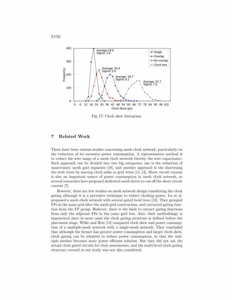
We generated the SPICE netlists of the three mesh implementations and a clocktree from the circuit ac97 with parasitics extracted, and conducted Monte Carlosimulation of 1,000 samples to evaluate clock skew variation. We obtained the ar-rival times of all clock sinks, and calculated the global clock skew by subtractingthe minimum arrival time from the maximum arrival time.
Fig. 17 shows the histogram of the clock skew for each clock network. Single-mesh network and clock tree show the smallest and the largest clock skew varia-tions, respectively. Multiple-mesh implementation with mesh overlap is affectedon-chip variation more than multiple meshes without overlap. It is due to itslonger latency; a mesh network of overlapped multiple meshes has longer wire-length and thereby more wire capacitance, so it shows larger clock latency thanfloorplaned meshes. Floorplanning the multiple meshes reduces the clock wire-length, so it can reduce the clock skew variation.
XVIII
0
100
200
300
400
0 6 12 18 24 30 36 42 48 54 60 66 72 78 84 90 96 102
Fre
quency
Clock Skew (ps)
Single
Overlap
No overlap
Clock tree
Average:19.5Sigma: 2.9
Average: 26.4Sigma: 5.6
Average: 38.7Sigma: 6.1
Average: 67.7Sigma: 7.9
Fig. 17: Clock skew histogram.
7 Related Work
There have been various studies concerning mesh clock network, particularly onthe reduction of its excessive power consumption. A representative method isto reduce the wire usage of a mesh clock network thereby the wire capacitance.Such approach can be divided into two big categories; one is the reduction ofunnecessary mesh grid segments [10], and another approach is the shorteningthe stub wires by moving clock sinks or grid wires [11,12]. Short circuit currentis also an important source of power consumption in mesh clock network, soseveral researches have proposed dedicated mesh driver to cut off the short circuitcurrent [7].
However, there are few studies on mesh network design considering the clockgating although it is a pervasive technique to reduce clocking power. Lu et al.proposed a mesh clock network with several gated local trees [13]. They groupedFFs in the same grid after the mesh grid construction, and extracted gating func-tion from the FF group. However, there is the limit to extract gating functionsfrom only the adjacent FFs in the same grid box. Also, their methodology isimpractical since in most cases the clock gating structure is defined before theplacement stage. Wilke and Reis [14] compared clock skew and power consump-tion of a multiple-mesh network with a single-mesh network. They concludedthat although the former has greater power consumption and larger clock skew,clock gating can be adopted to reduce power consumption, in that the mul-tiple meshes becomes more power efficient solution. But they did not use theactual clock gated circuits for their assessments, and the multi-level clock gatingstructure covered in our study was not also considered.
XIX
In [15], which is the preliminary version of this paper, Jung et al. in thefirst time consider practical multi-level clock gating structure in the design ofthe single-mesh and multiple-mesh network. They presented the comparison ofthe two mesh networks, and showed that the multiple-mesh network consumeslower power while the single-mesh has the advantages in clock skew and designcomplexity. It is also presented that the floorplanning of multiple meshes can beused to reduce the power consumption of multiple meshes at the cost of criticalpath delay.
8 Conclusion
The clock network of a design with hierarchical clock gating can be implementedby a set of meshes. If some hierarchies are removed, however, it also can be imple-mented by a single big mesh. We have shown that multiple-mesh implementationhas advantage in clock power (16.2% smaller power on average of test circuits);but single mesh consumes shorter clock wires, yields smaller clock skew, andtakes less time to design.
Multiple meshes can be floorplanned with some overlaps if placement is per-formed in flat, or they can be floorplanned without overlap if hierarchical physicaldesign is assumed. The experiments have shown that the mesh floorplan withoverlap yields smaller clock power owing to shorter clock wires, smaller clockskew, and more variation tolerance, but timing closure is easier if overlap arenot allowed.
References[1] Shin, Y., Shin, K., Kenkare, P., Kashyap, R., Lee, H.J., Seo, D., Millar, B., Kwon,
Y., Iyengar, R., Kim, M.S., Chowdhury, A., Bae, S.I., Hong, I., Jeong, W., Lind-ner, A., Cho, U., Hawkins, K., Son, J.C., Hwang, S.H.: 28nm high-k metal-gateheterogeneous quad-core CPUs for high-performance and energy-efficient mobileapplication processor. In: Proc. Int. Solid-State Circuits Conf. (February 2013)154–155
[2] Singh, T., Bell, J., Southard, S.: Jaguar: a next-generation low-power x86-64 core.In: Proc. Int. Solid-State Circuits Conf. (February 2013) 52–53
[3] Xu, K., Choy, C.S.: Low-power H.264/AVC baseline decoder for portable applica-tions. In: Proc. Int. Symp. on Low Power Electronics and Design. (August 2007)256–261
[4] Guthaus, M.R., Wilke, G., Reis, R.: Revisiting automated physical synthesis ofhigh-performance clock networks. ACM Trans. on Design Automation of Elec-tronic Systems 18(2) (April 2013) 31:1–31:27
[5] Chinnery, D.: High performance and low power design techniques for ASIC andcustom in nanometer technologies. In: Proc. Int. Symp. on Physical Design.(March 2013) 25–32
[6] Cyclos: Clock design for SoCs with lower power and better specs. http://www.cyclos-semi.com.
[7] Shim, S., Mo, M., Kim, S., Shin, Y.: Analysis and minimization of short-circuitcurrent in mesh clock network. In: Proc. Int. Conf. on Computer Design. (October2013) 459–462
XX
[8] Ezroni, J.: Advanced dynamic power reduction techniques: XOR self-gating.White paper (April 2011)
[9] OpenCores. http://www.opencores.org.[10] Rajaram, A., Pan, D.Z.: MeshWorks: A comprehensive framework for optimized
clock mesh network synthesis. IEEE Trans. on Computer-Aided Design of Inte-grated Circuits and Systems 29(12) (December 2010) 1945–1958
[11] Lu, J., Mao, X., Taskin, B.: Integrated clock mesh synthesis with incrementalregister placement. 31(2) (February 2012) 217–227
[12] Guthaus, M.R., Wilke, G., Reis, R.: Non-uniform clock mesh optimization withlinear programming buffer insertion. In: Proc. Design Automation Conf. (2010)74–79
[13] Lu, J., Mao, X., Taskin, B.: Clock mesh synthesis with gated local trees andactivity driven register clustering. In: Proc. Int. Conf. on Computer-Aided Design.(April 2012) 691–697
[14] Wilke, G.R.: Design and analysis of “tree+local meshes” clock architecture. In:Proc. Int. Symp. on Quality Electronic Design. (March 2007) 165–170
[15] Jung, J., Lee, D., Shin, Y.: Design and optimization of multiple-mesh clock net-work. In: Proc. Int. Conf. on VLSI and System-on-Chip. (October 2014) 171–176