Embed Size (px)
Citation preview

1
DesignCon 2011
Design and Optimization of a Novel 2.4 mm Coaxial Field Replaceable Connector Suitable for 25 Gbps System and Material Characterization up to 50 GHz David Dunham, Molex Inc. [email protected], +1-630-718-5817 Joon Lee, Molex Inc. [email protected], +1-317-834-5600 Scott McMorrow, Teraspeed Consulting Group [email protected], +1- 401- 284-1827 Yuriy Shlepnev, Simberian Inc. [email protected], +1-702-876-2882

2
Abstract With Data rates climbing to 10-12.5 Gb/s and plans for 28 Gb/s, it becomes important to increase PCB test fixture bandwidth from the typical 20 GHz to 50 GHz. There are several vendor Vector Network Analyzers that will sweep this high, but not many PCB launch connectors that can accurately launch these high frequencies. This paper will:
• Present modeling and validate data for a novel compression launch 2.4mm coaxial connector, functional up to 50GHz
• Show methods for analytical modeling and measurements for optimizing the PCB launch and escape under the 2.4 mm connector
• Demonstrate accurate broadband material characterization, using the method of generalized modal S-parameters, out to 50 GHz
The 2.4mm design includes a compression attach center conductor that does not require a solder attach to the PCB. The 2.4mm coax design meets all the standard 2.4mm mechanical interface standards, with a VSWR of <1.2 @ 50 GHz using back-to-back connector attachment. This paper will review EDA analytic modeling methodology and results for the integrated 2.4mm coaxial connector with several PCB layout designs. The final optimized PCB design was fabricated, measured and correlated to the analytical model. Author(s) Biography Dave Dunham is an Electrical Engineer in Connector Product Division at Molex. His primary focus is in design and characterization of next generation backplane and I/O systems and components. He has been also involved in the test and measurement methodologies, such as TRL calibration and 3.5mm field replaceable optimization. Dave has a BSEE degree from University of New Mexico. Joon Lee is a Sr. RF design engineer at Molex and his current work include design and optimization of RF transmission line links and interconnect components. Joon´s background also includes design of filter, antenna, connectors, and RF surge arrestors. He graduated from Virginia Tech with BSEE and has master´s from University of Illinois, at Chicago. Scott McMorrow is President and Founder of Teraspeed Consulting Group. Mr. McMorrow is an experienced technologist with over 20 years of broad background in complex system design, interconnect & Signal Integrity engineering, modeling & measurement methodology, engineering team building and professional training. Mr. McMorrow has a consistent history of delivering and managing technical consultation that enables clients to manufacture systems with state-of-the-art performance, enhanced design margins, lower cost, and reduced risk. Mr McMorrow is an expert in high-performance design and signal integrity engineering, and has been a consultant and trainer to engineering organizations world-wide.

3
Yuriy Shlepnev is President and Founder of Simberian Inc., where he develops Simbeor electromagnetic signal integrity software. He was principal developer of electromagnetic simulator for Eagleware Corporation and leading developer of electromagnetic software for simulation of high-speed digital circuits at Mentor Graphics. The results of his research are published in multiple papers and conference proceedings.

4
1. Introduction Design of connector launches up to 40-50 GHz requires electromagnetic analysis with
broadband causal dielectric and conductor models. Getting accurate broadband models for composite PCB and packaging dielectrics for such analysis is a very challenging task. Dielectric properties are typically available from a manufacturer at a few frequency points at best and more often just at one frequency, or without a frequency at all (extracted with TDR and static field solvers). Assumption that dielectric properties are frequency-independent can lead to unacceptable differences between the computational model and actual behavior of the structure. Conductor roughness can also contribute to discrepancies between models and experiment. Thus, we can observe that almost any serious multi-gigabit channel design project nowadays starts with, or includes, an in-house material characterization process. A brief review of the available material characterization techniques is provided in [1]-[2]. In this paper we will use a simple and practical procedure for the identification of dielectric parameters on the base of generalized modal S-parameters (GMS-parameters) suggested in [2]. The technique has been successfully used on multiple prototypes and production boards such as the test board featured in this paper.
The GMS-parameters material identification method is very accurate and the simplest possible. The material identification method is based on comparison of the GMS-parameters extracted from the measured S-parameters with GMS-parameters computed for a line segment by solving electromagnetic problem (no simulation of connector or launches is required). The key in such comparison is the minimal number or the parameters to match. Only generalized modal transmission parameters are not zero and are easy-to-use for the identification. Reflection and modal transition parameters of GMS-matrix are exactly zeroes. It simplifies the identification process a lot without sacrificing the accuracy of the process. It does not require multiple structures for broad-band TRL calibration and expensive 3D full-wave modeling of launches and connectors. Just two segments of line of any type and with theoretically any characteristic impedance and launches can be used to identify dielectric or conductor properties with high accuracy. Practically, performance of both connector and launch has to be optimal due to the limited dynamic range of the measurement equipment and possible non-locality of the launch return path. Transmission resonances in the connector and launch may substantially degrade GMS-parameters and limit the identification frequency range. In addition, the fields at the launch have be well localized up to the highest frequency of interest (50 GHz in our case) to insure that the launch does not depend on the board geometry and on other possible structures in the return path.
GMS-parameters based technique is based on the assumption that the connectors or probes and launches on the two test fixtures are substantially identical. In reality, both connectors and transitions are not identical. This paper investigates sensitivity of the GMS-parameters material identification method to variations in geometry of the launches, effective measurement bandwidth, and EM field containment in the launch region of a 2.4 mm compression attach connector.

5
2. Project goals The goals of the project are:
• Model and validate data for a novel compression launch 2.4mm coaxial connector, functional up to 50GHz
• Design optimal launch for the new 2.4 mm connector suitable for material characterization up to 50 GHz
• Build a set of test boards to validate connector and launch designs • Demonstrate accurate broadband material characterization, using the method of
generalized modal S-parameters, out to 50 GHz
3. Connector Design 3.1 Initial Design The connector interface that can handle up to 50 GHz was needed for this project.
The 2.4mm interface was selected due to its similar overall physical size as the current SMA connectors that are being used currently and similar compression contact attachment to PCB pad launch type design was preferred. The measurements of these connectors were done before the board was fabricated so the best way to measure its characteristic was to mate it back to back as shown in Fig. 3.5 below. This method proved to be best for measuring this compression contact style board connectors.
Initial design was setup for ease of connector manufacturing, assembly, and test but the preliminary results were not satisfactory mainly due to large signal reflection peak in the middle of the frequency band around 30 GHz as shown in Fig. 3.3. The rear body dimension for this connector is shown in Fig. 3.2.
Fig. 3.1: 2.4mm interface Fig. 3.2: Rear dimension

6
Fig. 3.3: Initial plot
3.2 Optimized connector The optimization of the connector included the changes to the back end of the
connector where the body ID and contact OD was reduced, (see Fig. 3.4) to minimize the signal reflections and shift any resonance that may exist within the 50 GHz frequency bandwidth. (Fig. 3.6) Since the center contacts are very small in size, they require consistent and accurate ways to clamp the two bodies together. For this reason, different set of body styles were manufactured that included larger flange with screw holes to let bolts and nuts to clamp the two bodies together. (Fig. 3.5) This helps the two center contacts to engage concentrically to firmly mate and compress against each other for accurate and stable measurements.
Fig. 3.4: Optimized rear dimension Fig. 3.5: Back-to-back
7
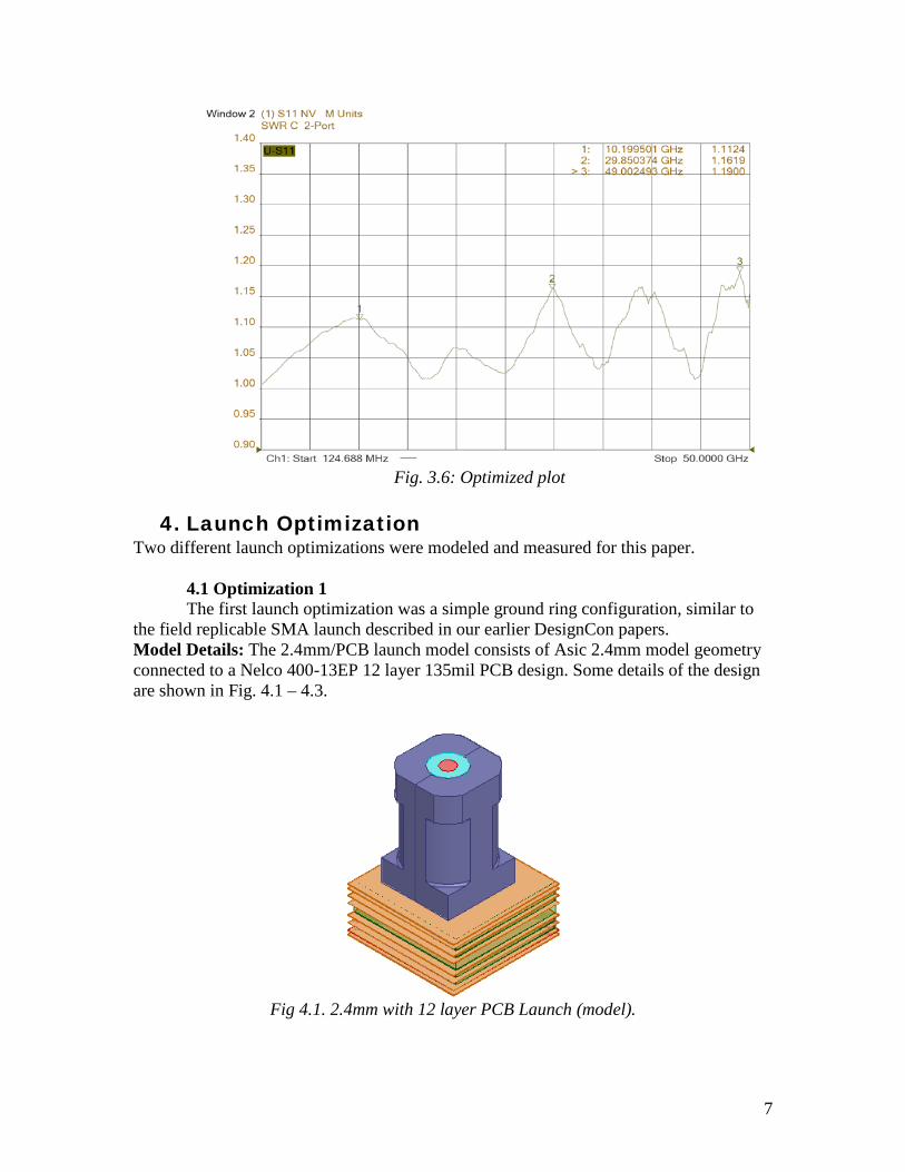
Fig. 3.6: Optimized plot
4. Launch Optimization
Two different launch optimizations were modeled and measured for this paper.
4.1 Optimization 1 The first launch optimization was a simple ground ring configuration, similar to
the field replicable SMA launch described in our earlier DesignCon papers. Model Details: The 2.4mm/PCB launch model consists of Asic 2.4mm model geometry connected to a Nelco 400-13EP 12 layer 135mil PCB design. Some details of the design are shown in Fig. 4.1 – 4.3.
Fig 4.1. 2.4mm with 12 layer PCB Launch (model).
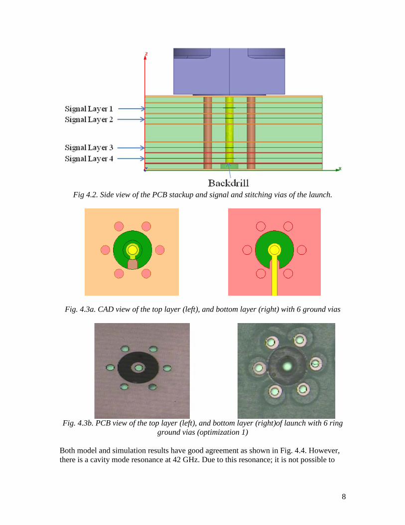
8
Fig 4.2. Side view of the PCB stackup and signal and stitching vias of the launch.
Fig. 4.3a. CAD view of the top layer (left), and bottom layer (right) with 6 ground vias
Fig. 4.3b. PCB view of the top layer (left), and bottom layer (right)of launch with 6 ring
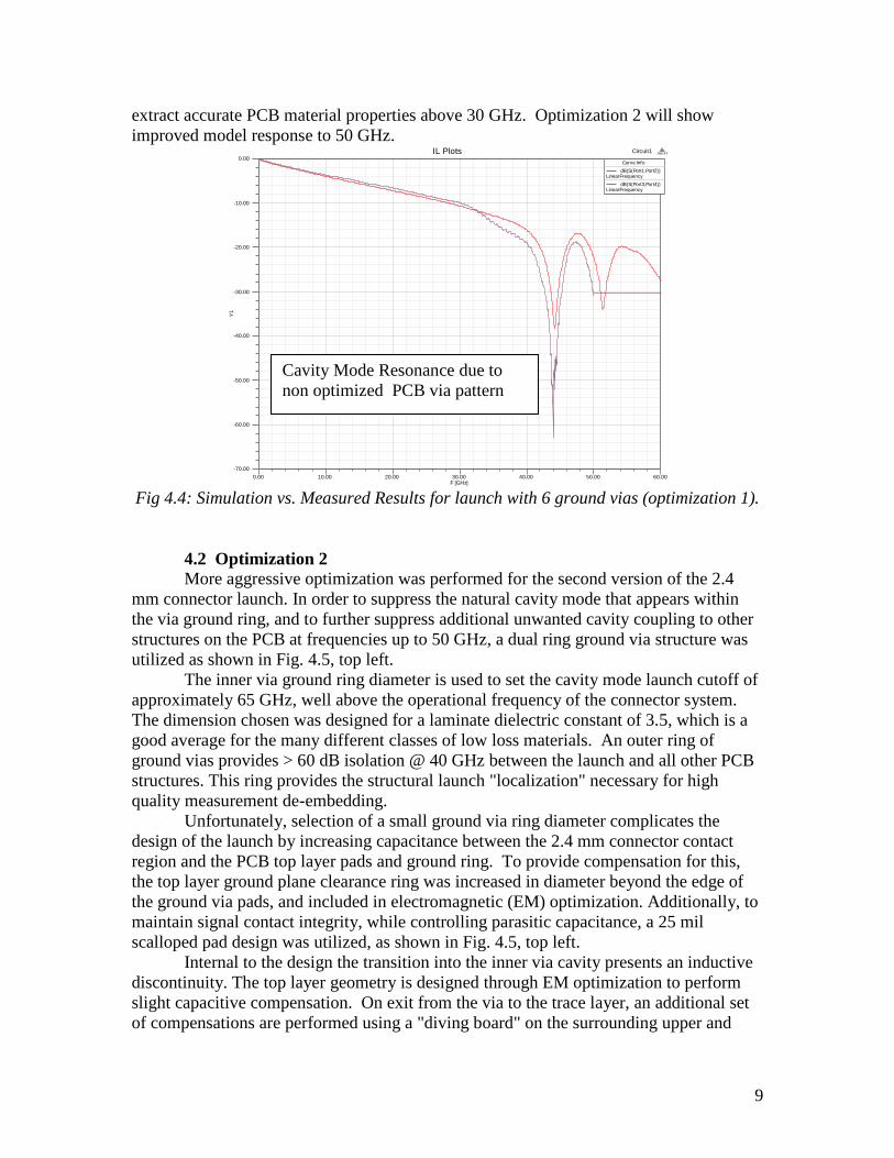
ground vias (optimization 1) Both model and simulation results have good agreement as shown in Fig. 4.4. However, there is a cavity mode resonance at 42 GHz. Due to this resonance; it is not possible to
9
extract accurate PCB material properties above 30 GHz. Optimization 2 will show improved model response to 50 GHz.
0.00 10.00 20.00 30.00 40.00 50.00 60.00F [GHz]
-70.00
-60.00
-50.00
-40.00
-30.00
-20.00
-10.00
0.00
Y1
Circuit1IL Plots ANSOFT
Curve InfodB(S(Port1,Port2))
LinearFrequencydB(S(Port3,Port4))
LinearFrequency
Fig 4.4: Simulation vs. Measured Results for launch with 6 ground vias (optimization 1).
4.2 Optimization 2 More aggressive optimization was performed for the second version of the 2.4
mm connector launch. In order to suppress the natural cavity mode that appears within the via ground ring, and to further suppress additional unwanted cavity coupling to other structures on the PCB at frequencies up to 50 GHz, a dual ring ground via structure was utilized as shown in Fig. 4.5, top left.
The inner via ground ring diameter is used to set the cavity mode launch cutoff of approximately 65 GHz, well above the operational frequency of the connector system. The dimension chosen was designed for a laminate dielectric constant of 3.5, which is a good average for the many different classes of low loss materials. An outer ring of ground vias provides > 60 dB isolation @ 40 GHz between the launch and all other PCB structures. This ring provides the structural launch "localization" necessary for high quality measurement de-embedding.
Unfortunately, selection of a small ground via ring diameter complicates the design of the launch by increasing capacitance between the 2.4 mm connector contact region and the PCB top layer pads and ground ring. To provide compensation for this, the top layer ground plane clearance ring was increased in diameter beyond the edge of the ground via pads, and included in electromagnetic (EM) optimization. Additionally, to maintain signal contact integrity, while controlling parasitic capacitance, a 25 mil scalloped pad design was utilized, as shown in Fig. 4.5, top left.
Internal to the design the transition into the inner via cavity presents an inductive discontinuity. The top layer geometry is designed through EM optimization to perform slight capacitive compensation. On exit from the via to the trace layer, an additional set of compensations are performed using a "diving board" on the surrounding upper and
Cavity Mode Resonance due to non optimized PCB via pattern

10
lower plane layers, and a widened lower impedance stepped trace transition, as shown in Fig. 4.5.
Fig. 4.5– Aggressive 2.4 mm connector launch. Top Left: Top layer of launch
structure showing via Top Right: Plane layer above and below trace . Bottom Left: Trace layer. Bottom Right: E-field strength on trace layer at 40.9 GHz, shows well
constrained and localized pattern, with low field leakage.
Final optimization of the launch design was performed with two connectors on the 12-layer PCB design with 0.3" of stripline trace, as shown in Fig. 4.6 and Fig 4.7. Previous experience has shown that optimization of a connector launch in isolation can lead to a poor result, due to the unevaluated potential resonance peaking that can occur between two connectors attached to the same trace. A more thorough optimization which includes the additional mismatch between two launch regions provides a more robust design. For the final optimization, the following design parameters were evaluated for a weighted minimization of return loss across five different frequency bands from 10 GHz to 50 GHz (dimensions in mils): GroundViaRadius = 34.9587 divingBoardWidth = 16.0426 innerAntipadTweek = 16.6858 topAntipadTweek = 18.7587

11
traceExitWidth = 8.95257 Total optimizer time = 04:36:20 h (50 evaluations)
Fig. 4.6 – Aggressive 2.4 mm connector launch optimizations. Top Left: Return loss sweeps. Top Right: TDR sweeps. Bottom Left: Optimized return loss. Bottom Right:
Two 2.4 mm connectors on PCB.
Fig. 4.7 PCB view of the top layer (left) and bottom layer (right) of launch with 17
ground vias (optimization 2)

12
5. Identification of dielectric model
Here are five steps of the dielectric identification procedure (Simberian’s patent pending):
1. Measure S-parameters of two test fixtures with different length of line segments - S1 and S2
2. Transform S1 and S2 to the T-matrices T1 and T2, diagonalize the product of T1 and inversed T2 and compute GMS-parameters of the line difference
3. Select material models and guess values of the model parameters 4. Compute GMS-parameters of the line difference segment by solving Maxwell’s
equation for t-line cross-section (only propagation constants are needed) 5. Adjust material parameters until computed GMS-parameters fit measured GMS-
parameters with the computed (or computed complex propagation constants match measured propagation constants)
Step 1. GMS-matrix of a line segment can be extracted from the measured S-parameters of 2 line segments with the length difference equal to dL . Following the procedure described in [2], we measure 2-port S-parameters for 2 strip or microstrip transmission line segments with VNA or TDNA. S-parameters should be pre-qualified first and have reciprocity and passivity quality measures above 99%. SOLT calibration is optional here because the identification procedure is self-calibrated. Let’s assume that we measured two S-parameter models: S1 for the fixture with continuous coupled line segment L1, and S2 for the fixture with the continuous line segment L2. Step 2. Following the procedure described in [4] we convert S-parameters into scattering T-parameters T1 and T2. As it was shown in [2], generalized modal T-parameters (GMT-parameters) of the line segment difference can be expressed as the eigenvalues of the product of T1 and inversed T2:
( )12 1GMT diag eigenvals T T − = ⋅ (5.1)
or 11
111
00
TGMT T − =
(5.2)
Due to the reciprocity of PCB and packaging materials, there is only 1 unique element in the GMT-parameters (5.2). Conversion of the GMT-parameters to GMS-parameters is straightforward and gives us measured GMS-parameters with just 1 unique non-zero elements:
11
11
00
TGMSm T =
(5.3)
Here 11T is generalized transmission parameter for a dominant mode in the transmission line – it is a hybrid quasi-TEM mode in PCB or packaging microstrip and strip lines. The measured generalized modal (GM) transmission parameters should correspond to the computed values. Note, that the measured GMS-parameter may appear noisy. This happens mostly due to non-identities of the investigated lines in two test fixtures, non-identities of the connectors and launches, and due to discontinuities (if straight lines are
13
not used). Note that the complex propagation constants of the t-line mode can be easily computed from 11T , though this step is not necessary here. Measured GMS-parameters can be additionally fitted with a square root of frequency and polynomial functions to get rid of small non-identity and measurement noise. Large non-identities in launch line cross-sections lead to extremely noisy and distorted GMS-parameters that cannot be improved or used for the identification [6]. Thus, the extraction fixture must be always optimized in advance and prequalified for the identification. Note, that further post-processing of (5.3) with the goal to extract complex propagation constants and further the properties of the dielectrics from the attenuation and phase constant looks like a good idea at first, but in reality such methods are typically based on closed-form expressions for the attenuation and phase constant. Expressions allow separation of polarization and conductive losses, but the results of such extraction are not accurate due to multiple assumptions in the closed-form expressions that lead to over-simplification of the problem. Step 3. As it was shown in [2], the wideband Debye (or Djordjevic-Sarkar) model provides good correlation for PCB dielectrics with relatively high losses. The model can be described with dielectric constant and loss tangent defined at one frequency point. Just one point defines causal analytical dependency of the complex dielectric constant from frequency. Recent studies showed that the wideband Debye model can be also used for the low-loss dielectrics if the conductor roughness is appropriately accounted for. Alternatively, a multi-pole Debye model also described in [2] can be used – any dielectric mixture with decreasing dielectric constant and any type of loss tangent behavior can be fitted with the multiple Debye poles. Conductor roughness parameters should be also specified at this step to ensure accurate polarization loss identification. Step 4. If single-ended lines are used for the identification, GMS-parameters of a line segment form a 2 by 2 complex matrix with very simple structure:
( )( )
0 expexp 0
dLGMSc dL−Γ ⋅ = −Γ ⋅
(5.4)
Here dL is the length of the line segment, and ( ) ( ) ( )f f i fα βΓ = + ⋅ is the complex propagation constant of the dominant mode in the transmission line. The most attractive and useful property of GMS-parameters of t-line lines (5.3) and (5.4) is simplicity – only 1 unique non-zero element and independence of the characteristic impedance. Absence of reflection can be simply explained by the fact that GMS-parameters are normalized to the complex characteristic impedance of the line. This is valid in the case of measured GMS-parameters (5.3) and in the case of corresponding model (5.4). In both cases the actual characteristic impedances are not needed. The impedance can be computed in the numerical model if necessary for calibration or de-embedding purpose. The propagation constant is frequency dependent in general and has to be extracted by solving the Maxwell’s equation for a cross-section of the transmission line or extracted from 3D EM analysis of a line segment with the simultaneous diagonalization method [2] implemented in Simbeor software [3] used in this paper. Only full-wave analysis with causal dispersive models of dielectrics and conductors is suitable for the identification of material properties up to 50 GHz. Use of approximate microstrip or strip line models

14
should be avoided because it introduces additional errors due to low accuracy of such models in general. Analysis with a static field solver can be used for the identification, but the bandwidth of such models are usually restricted to 3-5 GHz for PCB and packaging application due to low-accuracy modeling of dielectric and conductor effects and complete absence of high-frequency dispersion modeling. The results of identification with approximate models may be considered only as a crude low-frequency approximation. Step 5. We first match the computed phase or group delay of the generalized modal transmission coefficients (5.4) to the measured values (5.3) by tuning only dielectric constant in the wideband or multi-pole Debye model and re-simulating the line segment. After the phase and group delay are matching with a desirable accuracy, the next step is to adjust the dielectric model loss tangent to have magnitudes of the computed generalized modal transmission coefficients (5.4) matching the measured values (5.3). Note that appropriate conductor roughness model is essential for the identification of the polarization losses, especially in case of low-loss dielectrics. Technically, matching generalized insertion loss is equivalent to matching the attenuation part of the computed and measured complex propagation constants. Matching of the phases of generalized transmission parameters is equivalent to matching of the phase constant parts of the computed and measured complex propagation constants. The final dielectric model is the one that produces the best match between computed and measured GMS-parameters or between computed and measured complex propagation constants. Such model should produce expected correlation in the analysis of interconnects with reasonable variations of geometry of the cross-section. The outlined material identification technique with GMS-parameters is the simplest possible for interconnect applications and the reasons are as follows: • Needs un-calibrated measurements for two transmission line segments with any
geometry of cross-section and transitions • No de-embedding of connectors and launches (difficult, error-prone) • Needs the simplest numerical model
o Requires computation of only propagation constants o No 3D electromagnetic models of launches and connectors
• Minimal number of smooth complex functions to match o One parameter for single and two parameters for differential o All reflection and modal transformation parameters are exactly zeros
6. Sensitivity of GMS-parameters to non-identity of
launches in test coupons To investigate the effect of launch non-identity on measured GMS-parameters we
will use a numerical experiment here. Stackup and initial mock-up launch geometry for the experiment are shown in Fig. 6.1. We first simulate 6 and 8 inch test fixtures with varying geometry of the launches on both sides and next convert numerically extracted S-parameters of the pair of test fixtures into GMS-parameters of the difference (5.3). Then we compare it with GMS-parameters computed directly for the strip line segment (5.4) with dL equal 2 inches in this case. Ideally the results should match exactly, and the

15
difference in the GMS-parameters computed by two methods will be the error introduced by the launches non-identity. We will then quantify acceptable error in terms of some non-identity measures. Fast decompositional analysis with the full-wave 3D models created separately for the launches and for the transmission line segments is used for the analysis.
Fig. 6.1. Simplified stackup and launch for numerical investigation of launch non-
identity effect on GMS-parameters. Let’s first investigate the S-parameters of the test fixtures with different diameters of the pads in the strip-line layer. Changes of diameter of the strip pad causes changes in the reflection loss from the single launch as shown on the left graph of Fig. 6.2. Larger pad diameter will increase pad capacitance and increase reflection loss. We can observe clear correlation of the reflection from a single launch with the reflection from the test fixture with 2 launches and 8-inch segment of strip line shown on the right graph in Fig. 6.2 (parameters of 6-inch structure is similar). There are additional oscillations on the right graph due to small mismatch of the transmission line impedance and 50 Ohm normalization.
Fig. 6.2. Reflection from the launches with different pad diameter (left graph) and
reflection from 8-inch test fixture with 2 launches (right graph).

16
As we can see, the launches are not ideal and mostly capacitive in this case. That is typical for a design exploration project when the material properties are not known in advance – any optimization of such launch with guessed material parameters is a waste of time and money. Use of the transmission parameters with non-ideal launches for the material identification is also very ambiguous. For instance, the insertion loss depends on the diameters of the pads as shown in Fig. 6.3. If we neglect the reflection (that nobody should do even in the case of “very transparent” launches), it will lead to large errors in the identification of loss parameters such as loss tangent for dielectric or roughness parameters for conductors.
Fig. 6.3. Effect of the launch pad diameter on the insertion loss of 8-inch test fixture with
2 launches (right graph). Nevertheless, some authors still neglect the reflection that may lead to inaccurate conclusions on the material properties [7]. Note also that even if the parameters of the materials are identified and the launches are optimized (that is actually a Catch 22), the manufacturing tolerances and fibers in PCB dielectrics makes the launches slightly different. This may lead to large differences in the reflection loss and finally to wrong conclusions concerning the materials properties. Thus, the best way to do the material identification (or confirmation of the identification) is to get rid of the reflection at the launches. This is exactly what conversion to the GMS-parameters does. GMS-parameters extracted from the 6 and 8 inch test fixtures are shown in Fig. 6.4. In the case where all 4 launches in one pair used for extraction are identical, the results are exactly as if we compute GMS-parameters of 2-inch segment of strip line. It is obvious that the reflective property of the launch (and connector) does not have effect on the GMS-parameters as long as all launches are identical (this is a theoretical statement – in reality the dynamic range of the measurement equipment is limited and the connectors and launches have to be optimized to keep the insertion loss above the noise floor of the VNA or TDNA). But, what if the launches on the test fixtures in one pair are different? Let’s try to extract GMS-parameters from two test fixtures that have different launches. The launches on the same test fixture will be identical. The

17
magnitudes and group delays for different variations of launches are plotted in Fig. 6.5-6.7. We can see that 3.5 mil difference in the pad diameter on the launches causes similar looking “noise”-like deviations (blue lines) from the accurate values of magnitude and group delay (red stars). Some pairs have visibly larger noise (6.7) and some produce smaller noise (Fig. 6.6). Use of pairs of launches with smaller 2 mil difference in pad diameters expectedly produces much smaller “noise” on the generalized modal insertion loss and group delay as shown in Fig. 6.8.
Fig. 6.4. GMS transmission parameters extracted from 6 and 8 inch test fixtures with 8 mil pads on all launches (left graph) and with 22 mil pads on all launches (stars) and
GSM-parameters of 2-inch strip line. The correspondence is exact and independent of the reflection.
Fig. 6.5. GMS transmission parameters extracted from 6 inch test fixture with 8 mil pads and 8 inch fixture with 11.5 mil pads – blue lines. Red stars – exact solution for 2-inch
line segment.

18
Fig. 6.6. GMS transmission extracted from 6 inch test fixture with 11.5 mil pads and 8
inch fixture with 15 mil pads – blue lines. Red stars – exact result for 2-inch line segment.
Fig. 6.7. GMS transmission extracted from 6 inch test fixture with 18.5 mil pads and 8
inch fixture with 22 mil pads (blue lines). Red stars – exact result for 2-inch line segment.
Fig. 6.8. GMS transmission extracted from 6 inch test fixture with 15 mil pads and 8 inch fixture with 13 mil pads – blue lines. Red stars – exact solution for 2-inch line segment.

19
Differences of GMS-parameters extracted from two test fixtures with different diameters of the launch pads and exact GMS-parameters of 2-inch strip line are shown in Fig. 6.9. Technically these plots characterize the extraction errors caused by differences in the launches. If launches T3 used on 6-inch fixture and T4 on 8-inch fixture the error is the maximal as we can see in Fig. 6.7 and in Fig. 6.9 (red line). If we use two launches with the smaller difference in diameter (Fig. 6.8), the GMS-parameters computation error is significantly reduced as shown by black line in Fig. 6.9.
Fig. 6.9. Error in GMS parameters extracted from structures with different launches.
Pair of launches T3-T4 produces largest error (red line), pair of launches T2-TM produces the smallest error (black line).
Fig. 6.10. Differences of the reflection parameters of the launches with different pad diameters. Small changes on more reflective launches lead to larger variations in S-
parameters in general.

20
To quantify the expected errors we first take a look at the reflection difference between launches with different pad diameters shown in Fig. 6.10. The same 3.5 mil change in diameter of the most reflective launches T4 and T3 lead to the largest difference in the S-parameters of the launches (line with squares in Fig. 6.10) and to the largest error in the extracted GMS-parameters. Smaller differences in the S-parameters of the launches (Fig. 6.10) leads to smaller errors in the final GMS-parameters (Fig. 6.9). A pair of launches with 2 mil difference in diameter has the smallest difference in the S-parameters of the launches and produces the smallest error in the extracted GMS-parameters as expected.
Note that the least reflective launch with pad diameter T0 (see Fig. 6.2) has relatively large S-parameters difference with the launch T1. Though, the difference in the pad diameters of pair T0-T1 is the same 3.5 mil as for all other combinations of the launches shown in red lines in Fig. 6.10. The “tuned” launch may be highly sensitive to the variations of geometry and material properties. It means that the goal of launch design for the material characterization should be different from a design of non-reflective launch for a data channel for instance. The goal of the connector/probe + launch design should be geometry with S-parameters with minimal sensitivity to the manufacturing tolerances and to the in-homogeneity of materials. This is in addition to the non-resonant insertion loss requirement: the smaller the expected difference in S-parameters of the launches, the better. We can also expect that the less reflective connectors and launches may produce smaller differences in S-parameters. The question remains is how we can actually estimate whether the connectors or probes and launches on the test fixtures are acceptable for the identification of material properties. We actually do not know in advance the actual deviations of geometry and the effect of in-homogeneity of materials in the connector + launch structure. Time-domain reflectometry of the manufactured test fixtures can be used for a pre-qualification of the structures for GMS-parameters extraction and for the material identification. In case of our numerical experiment, we have 6 possible launch geometries on both 6 and 8 inch test fixtures. TDR for all of them is shown in Fig. 6.11.
Fig. 6.11. TDR of all six launches used in GMS-parameters extraction. Only 2 pairs
of structures can be used to extract GMS-parameters up to 50 GHz.
21
Only two combinations of launches T1&TM and T2&TM provided relatively small error in GMS-parameters up to 50 GHz. From TDR plots we can observe that launches TM, T1 and T2 have difference in the impedance profile less than 1 Ohm. All structures with the larger differences produced un-acceptable error in the GMS-parameters.
Real test coupons used for the material identification on a board may have not only differences in the connectors/probes and launches, but also differences in the geometry of transmission lines. Cross-sections of the transmission lines in two test fixtures may be different due to manufacturing process and weave effect. Transmission line segments may have discontinuities. All that can further degrade the extracted GMS-parameters and may distort the extracted dielectric parameters as shown in [6].
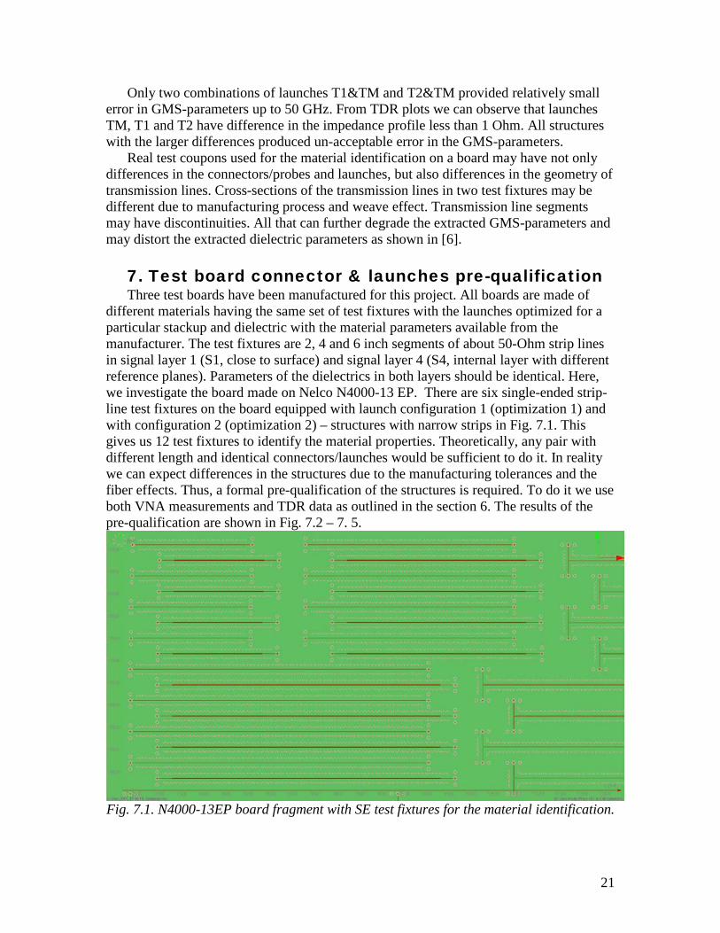
7. Test board connector & launches pre-qualification Three test boards have been manufactured for this project. All boards are made of
different materials having the same set of test fixtures with the launches optimized for a particular stackup and dielectric with the material parameters available from the manufacturer. The test fixtures are 2, 4 and 6 inch segments of about 50-Ohm strip lines in signal layer 1 (S1, close to surface) and signal layer 4 (S4, internal layer with different reference planes). Parameters of the dielectrics in both layers should be identical. Here, we investigate the board made on Nelco N4000-13 EP. There are six single-ended strip-line test fixtures on the board equipped with launch configuration 1 (optimization 1) and with configuration 2 (optimization 2) – structures with narrow strips in Fig. 7.1. This gives us 12 test fixtures to identify the material properties. Theoretically, any pair with different length and identical connectors/launches would be sufficient to do it. In reality we can expect differences in the structures due to the manufacturing tolerances and the fiber effects. Thus, a formal pre-qualification of the structures is required. To do it we use both VNA measurements and TDR data as outlined in the section 6. The results of the pre-qualification are shown in Fig. 7.2 – 7. 5.
Fig. 7.1. N4000-13EP board fragment with SE test fixtures for the material identification.

22
Fig. 7.2. Pre-qualification of launches on N4000-13EP board with launch 1 and strip line in layer S1.
Fig. 7.3. Pre-qualification of launches on N4000-13EP board with launch 1 and strip line
in layer S4.
23
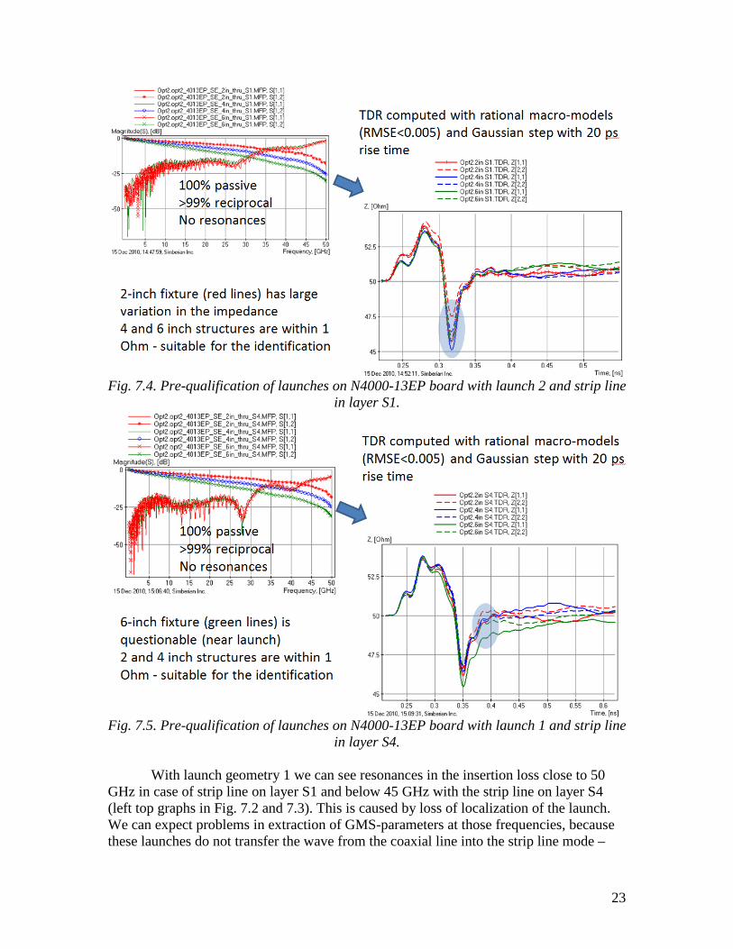
Fig. 7.4. Pre-qualification of launches on N4000-13EP board with launch 2 and strip line
in layer S1.
Fig. 7.5. Pre-qualification of launches on N4000-13EP board with launch 1 and strip line
in layer S4.
With launch geometry 1 we can see resonances in the insertion loss close to 50 GHz in case of strip line on layer S1 and below 45 GHz with the strip line on layer S4 (left top graphs in Fig. 7.2 and 7.3). This is caused by loss of localization of the launch. We can expect problems in extraction of GMS-parameters at those frequencies, because these launches do not transfer the wave from the coaxial line into the strip line mode –

24
they also excite waves between the parallel planes that are not confined by the stitching vias surrounding the signal via. In addition to the resonances, the 6-inch fixture in layer S1 and 2-inch fixture in layer S4 have launch impedance deviation larger than the 1-Ohm target. Launch geometry 2 shows better performance in the frequency domain (left top graph in Fig. 7.4 and 7.5) due to better localization – no resonances up to 50 GHz. At the first glance everything looks perfect, but TDR investigation reveals unacceptable impedance variations in the 2-inch test fixture on layer S1 and in 6-inch test fixture on layer S4. The defects are probably related to the position of the launch over the glass fiber (layer S4) or/and back-drilling tolerance (for layer S1).
Fig. 7.6. GMS-parameters extracted from the pre-qualified test fixtures.
Fig. 7.7. GMS-parameters extracted from the pre-qualified test fixtures.
Note that the impedance on the connector side and in the transition from the
connector to via is very consistent between different configurations with the same launch.

25
The exception is the launch on the 2-inch fixture with strip line on layer S4 and launch 1 configuration – the impedance looking from port 1 has large deviation between 0.25 and 0.3 ns - red line in Fig. 7.2.
Nearly all test fixtures are acceptable for practical material identification up to 35-40 GHz. The exceptions are pairs that include 2-inch line on layer S1 with launch 2 – the variation of impedance at the transition from the back-drilled via to the strip line reduces the identification frequency band to 20-25 GHz. Finally, only 3 pairs are acceptable for the identification up to 50 GHz. Extracted GMS-parameters for those pairs are plotted in Fig. 7.6. The “noise” at high frequencies is the result of the remaining non-identities of the test fixtures. It can be easily filtered out with fitting. The results are shown in Fig. 7.7. The fitted GMS-parameters can be used for precise identification of the material properties including separation of losses from conductor and dielectric.
8. Practical material identification Practical material identification begins with the launch pre-qualification of section 7
to find the "most suitable" test structures for material parametric fitting. For Nelco 4000-13EP PCB design, pre-qualification shows that the measurements performed on stripline layer 4 were superior. Three lines are therefore used in our process: a 2", 4" and 6" line on Layer 4 with the aggressive option 2 connector launch, which are used to de-embed two sets of 2" and one 4" GMS parameters.
The material identification process begins with a baseline value of dielectric constant from fitted GMS group delay. Fig. 8.1 shows this process on our 2" and 4" lines with an extracted Er of approximately 3.8. This will be used as the first approximation for our material identification process, and is in the same range as the manufacturer specified dielectric constant.
Fig. 8.1. GMS fitted group delay for 2" and 4" de-embedded traces show
dielectric constant of about 3.8.
Our modeled stackup includes the possibility of core and prepreg laminates with different characteristics for each section of the stripline layered dielectric. As a first approximation we will assume that both prepreg and core laminates have properties that are similar. This is a good approximation for our design, since both core and prepreg use the same fiberglass fabric and similar epoxy/glass ratios. If strongly dissimilar dielectric

26
layers are used, additional design of experiments and measurements may be necessary to effectively isolate the material properties of these layers.
Since we are dealing with anisotropic materials with fiberglass fabric, it is reasonable to expect that some variation will be seen in our measured samples. Fitted GMS group delay provides a valuable method of determining the variation in our selected traces. Fig. 8.2 shows that even in our selected samples, slight variations in trace propagation characteristics occur due to anisotropic laminate variations, most likely due to trace position over the laminate weave.
Fig. 8.2. GMS fitted group delay variation for 2" selected traces of 1 ps/in @50
GHz, 300 fs/in @ 20 GHz
Next, conductor resistance is then adjusted as shown inFig. 8.3 to obtain a good match for the raw unfiltered GMS data for our traces. Although annealed copper has a resistance of 1.724 ohm-m, most rolled and electroplated coppers used for copper foil will have a relative resistance of 1.05 to 1.45 that of annealed copper. Resistivity is adjusted at low frequency to show a good match between modeling and measurement. Additional measurements of wide traces and traces of different lengths can be used to discern resistivity of copper vs. that of the trace cross-section itself. In our case, using the known trace fabrication geometry led to good first pass success in determining trace conductor resistance. (Wide trace widths are a help in this regards.)

27
Fig. 8.3. GMS raw insertion loss is used at low frequency as a guide to adjust the
model resistivity. Once the model has been adjusted for average dielectric constant and copper
conductivity, a suitable dielectric loss model can be chosen. Dielectric constant is adjusted in the model to provide a close match at a low frequency of 1 GHz, while dielectric loss tangent is adjusted for a good high frequency match for group delay, as shown in Fig. 8.4. Typically a Djordjevic-Sarkar (Wideband Debye) [5] model is used to model most PCB and packaging materials. If a D-S model fit to group delay is not achievable, then a multi-pole Debye model [5] can be used (typically 8-10 poles are necessary to fit GMS-parameters from DC up to 50 GHz).
Fig. 8.4. GMS fitted group delay is used to guide adjustment of dielectric loss and
final adjustment for dielectric constant. After dielectric loss and dielectric constant have been adjusted, all that remains is
an adjustment of conductor surface roughness properties to match GMS insertion loss at various trace lengths with our trace electromagnetic model as shown in Fig. 8.5. In

28
our case, the material parameters fitted where Er = 3.8, tanD = 0.0076, Cu resistivity = 1.81e-8 ohm-m, Cu surface roughness = 0.55 micron RMS (roughness factor 2).
Fig. 8.5. GMS fitted attenuation variation for 2" and 4" selected traces with final
model.
Electromagnetic models derived using these methods have been correlated to multiple materials in multiple electromagnetic modeling tools with high precision. This base understanding of the material properties derived from this method can now be perturbed by known, measured, or guesstimated material variation across manufacturing processes, and used as an enabling technology for robust design.
9. Conclusion The main result of this paper is a practical methodology for extremely broad-band identification of the material parameters from DC up to 50 GHz. The methodology is based on three elements: design of low-reflective connector, design of non-resonant localized launch for the connector and precise material identification on the base of generalized modal S-parameters (GMS-parameters). The paper illustrated all three elements in detail. A novel compression-launch 2.4mm coaxial connector, functional up to 50GHz has been designed. We have stated goals and presented methodology for design of optimal PCB launch and escape under the 2.4 mm connector. We have outlined a GMS-based material identification procedure (it can be considered as an iterative refinement of the method proposed in [2]). It was shown that the material identification accuracy depends on the quality of the measured GMS-parameters. We have investigated sensitivity of GMS-parameters to non-identities of the launches geometries. It was shown that the larger the difference in S-parameters of the launches, or in the impedance profiles of the launches, the larger the GMS-parameters computation error and the more uncertain the material identification procedure. For practical material identification up to 50 GHz, the difference in the impedance profiles of launches should be less than 1 Ohm. We have illustrated it with pre-qualification of the launches on the test board with TDR measurements. Finally, we have shown that the appropriately designed connector and launch enable precise PCB material identification up to 50 GHz.

29
References 1. Y. Shlepnev, A. Neves, T. Dagostino, S. McMorrow, Measurement-Assisted
Electromagnetic Extraction of Interconnect Parameters on Low-Cost FR-4 boards for 6-20 Gb/sec Applications, DesignCon2009, http://www.designcon.com/infovault/
2. Y. Shlepnev, A. Neves, T. Dagostino, S. McMorrow, Practical identification of dispersive dielectric models with generalized modal S-parameters for analysis of interconnects in 6-100 Gb/s applications, DesignCon2010, http://www.designcon.com/infovault/
3. Simbeor 2011 Electromagnetic Signal Integrity Software, www.simberian.com 4. Seguinot et al.: Multimode TRL – A new concept in microwave measurements,
IEEE Trans. on MTT, vol. 46, 1998, N 5, p. 536-542. 5. Djordjevic, R.M. Biljic, V.D. Likar-Smiljanic, T.K.Sarkar, Wideband frequency
domain characterization of FR-4 and time-domain causality, IEEE Trans. on EMC, vol. 43, N4, 2001, p. 662-667.
6. Sensitivity of PCB Material Identification with GMS-Parameters to Variations in Test Fixtures, Simberian App Note #2010_03, available at http://simberian.com/AppNotes.php
7. A. F. Horn, III, J. W. Reynolds, and J. C. Rautio, Conductor Profile Effects on the Propagation Constant of Microstrip Transmission Lines, 2010 IEEE MTT International Symp. Digest, p. 868-871.