Embed Size (px)
Citation preview

Design and Implementation of a X-bandTransmitter and Frequency
Distribution Unit for a SyntheticAperture Radar
Darren Grant Coetzer
A dissertation submitted to the Department of Electrical Engineering,
University of Cape Town, in fulfilment of the requirements
for the degree of Master of Science in Engineering.
Cape Town, May 2004

Declaration
I declare that this dissertation is my own, unaided work. It is being submitted for the
degree of Master of Science in Engineering at the Universityof Cape Town. It has not
been submitted before for any degree or examination in any other university.
Signature of Author . . . . . . . . . . . . . . . . . . . . . . . . . . . . . . . . . .. . . . . . . . . . . . . . . . . . . . . . . . . . . .
Cape Town
24 May 2004
i

Abstract
Synthetic aperture radar (SAR) can provide high-resolution images of extensive areas of
the earth´s surface from a platform operating at long ranges, despite adverse weather con-
ditions or darkness. A local consortium was established to demonstrate a consolidated
South African SAR ability to demonstrate to the local and international communities, by
generating high quality images with a South African X-band demonstrator. This disser-
tation forms part of the project. It aims to describe the design and implementation of the
transmitter and associated frequency distribution unit (FDU) for the SASAR II, X-band
SAR.
Although the transmitter and FDU are two separate units, they are ultimately linked. The
transmitter has the task of taking a low-power, baseband, chirp waveform and, through a
series of mixers, filters and amplifiers, converting it to a high-power, microwave signal.
The FDU is essentially the heart of the transceiver and provides drive to all the mixer
local oscillator (LO) inputs. It also clocks the DAC and ADC which allow the essentially
analogue transceiver to communicate with the digital circuitry.
It is found that the chirp signal produced is of satisfactoryfidelity. LO feedthrough, how-
ever, is superimposed at the chirps´ centre frequency. As a result of previous stages, spu-
rious signals exist at 16 MHz offset from the chirps´ centre frequency and at 9142 MHz.
The system transfer function reveals that 2 dB roll-off is present at the outer frequencies
of the chirp signal. Group delay in the transmitter filters and amplifiers is held responsible
for this.
ii

Acknowledgements
I would most sincerely like to thank my supervisor, Professor Michael Inggs, for his
guidance, support and tolerance throughout the extent of the project. I have benefitted
immensely from his wealth of knowledge, from which he has most generously dispensed
over the past years. I am also in his debt for help with financial assistance, without which
nothing would have been possible.
I would also like to thank Richard Lord and Thomas Bennett, who were always there for
me, whenever help was needed. The rest of the Radar Remote Sensing Group (RRSG)
who put up with me over the past two years also deserve a special mention. Without them,
it would have been a far less enjoyable experience.
And finally, to my family, who have all supported me in everything I have done throughout
my life. Your encouragement, kindness and love have made everything possible and
worthwhile.
iii

Contents
Declaration i
Abstract ii
Acknowledgements iii
List of Symbols xi
Nomenclature xii
1 Introduction 1
1.1 Terms of Reference . . . . . . . . . . . . . . . . . . . . . . . . . . . . . 3
1.2 Plan of Development . . . . . . . . . . . . . . . . . . . . . . . . . . . . 4
2 Background Information 6
2.1 Project Background . . . . . . . . . . . . . . . . . . . . . . . . . . . . . 6
2.2 Basic SAR Theory . . . . . . . . . . . . . . . . . . . . . . . . . . . . . 6
2.3 System Overview . . . . . . . . . . . . . . . . . . . . . . . . . . . . . . 9
2.4 The Transmitter . . . . . . . . . . . . . . . . . . . . . . . . . . . . . . . 10
2.4.1 Chirp Formation and First Upconversion (IF1) . . . . . . .. . . 11
2.4.2 Second Upconversion (IF2) . . . . . . . . . . . . . . . . . . . . 11
2.4.3 Final Upconversion (RF) . . . . . . . . . . . . . . . . . . . . . . 11
2.4.4 Power Amplifier (PA) . . . . . . . . . . . . . . . . . . . . . . . 11
2.4.5 Built in test (BIT) . . . . . . . . . . . . . . . . . . . . . . . . . . 11
2.5 Frequency Distribution Unit . . . . . . . . . . . . . . . . . . . . . . .. 12
2.5.1 DAC and ADC Clocks . . . . . . . . . . . . . . . . . . . . . . . 12
2.5.2 Mixer Drives . . . . . . . . . . . . . . . . . . . . . . . . . . . . 12
3 Transmitter Design and Implementation 13
3.1 Chirp Theory and Simulation . . . . . . . . . . . . . . . . . . . . . . . .13
3.2 Mixers and Filters . . . . . . . . . . . . . . . . . . . . . . . . . . . . . . 22
iv

3.2.1 IF1 . . . . . . . . . . . . . . . . . . . . . . . . . . . . . . . . . 23
3.2.2 IF2 . . . . . . . . . . . . . . . . . . . . . . . . . . . . . . . . . 24
3.2.3 RF . . . . . . . . . . . . . . . . . . . . . . . . . . . . . . . . . . 25
3.3 BIT . . . . . . . . . . . . . . . . . . . . . . . . . . . . . . . . . . . . . 26
3.4 Power Requirements of Proposed Transmitter . . . . . . . . . .. . . . . 28
3.4.1 Power Levels . . . . . . . . . . . . . . . . . . . . . . . . . . . . 29
3.4.2 Waveguide Power-carrying Capacity . . . . . . . . . . . . . . .. 31
3.5 Summary . . . . . . . . . . . . . . . . . . . . . . . . . . . . . . . . . . 31
4 Design and Implementation of Frequency Distribution Unit 33
4.1 Frequency Synthesizers . . . . . . . . . . . . . . . . . . . . . . . . . . .33
4.2 Power Issues . . . . . . . . . . . . . . . . . . . . . . . . . . . . . . . . 35
4.3 Circuit Board Design . . . . . . . . . . . . . . . . . . . . . . . . . . . . 35
4.4 Amplifiers . . . . . . . . . . . . . . . . . . . . . . . . . . . . . . . . . . 37
4.5 Microwave Housing Design . . . . . . . . . . . . . . . . . . . . . . . . 40
4.6 Phase Noise and Jitter . . . . . . . . . . . . . . . . . . . . . . . . . . . . 41
4.7 Summary . . . . . . . . . . . . . . . . . . . . . . . . . . . . . . . . . . 42
5 Testing 44
5.1 Introduction . . . . . . . . . . . . . . . . . . . . . . . . . . . . . . . . . 44
5.2 Amplifier Testing . . . . . . . . . . . . . . . . . . . . . . . . . . . . . . 45
5.2.1 Equipment Used . . . . . . . . . . . . . . . . . . . . . . . . . . 45
5.2.2 Test Procedure . . . . . . . . . . . . . . . . . . . . . . . . . . . 45
5.2.3 Test Results . . . . . . . . . . . . . . . . . . . . . . . . . . . . . 45
5.3 Synthesizer Testing . . . . . . . . . . . . . . . . . . . . . . . . . . . . . 47
5.3.1 Equipment Used . . . . . . . . . . . . . . . . . . . . . . . . . . 47
5.3.2 Test Procedure . . . . . . . . . . . . . . . . . . . . . . . . . . . 48
5.3.3 Test Results . . . . . . . . . . . . . . . . . . . . . . . . . . . . . 48
5.4 Power Levels of the FDU . . . . . . . . . . . . . . . . . . . . . . . . . . 51
5.4.1 Equipment Used . . . . . . . . . . . . . . . . . . . . . . . . . . 51
5.4.2 Test Procedure . . . . . . . . . . . . . . . . . . . . . . . . . . . 51
5.4.3 Test Results . . . . . . . . . . . . . . . . . . . . . . . . . . . . . 52
5.5 Power Levels of the Transmitter . . . . . . . . . . . . . . . . . . . . .. 52
5.5.1 Equipment Used . . . . . . . . . . . . . . . . . . . . . . . . . . 52
5.5.2 Test Procedure . . . . . . . . . . . . . . . . . . . . . . . . . . . 52
5.5.3 Test Results . . . . . . . . . . . . . . . . . . . . . . . . . . . . . 52
v

5.6 Chirp Integrity . . . . . . . . . . . . . . . . . . . . . . . . . . . . . . . 52
5.6.1 Equipment Used . . . . . . . . . . . . . . . . . . . . . . . . . . 52
5.6.2 Test Procedure . . . . . . . . . . . . . . . . . . . . . . . . . . . 53
5.6.3 Test Results . . . . . . . . . . . . . . . . . . . . . . . . . . . . . 53
5.7 Spurious Signals . . . . . . . . . . . . . . . . . . . . . . . . . . . . . . 57
5.7.1 Equipment Used . . . . . . . . . . . . . . . . . . . . . . . . . . 57
5.7.2 Test Procedure . . . . . . . . . . . . . . . . . . . . . . . . . . . 57
5.7.3 Test Results . . . . . . . . . . . . . . . . . . . . . . . . . . . . . 58
5.8 System Transfer Function . . . . . . . . . . . . . . . . . . . . . . . . . .63
5.8.1 Equipment Used . . . . . . . . . . . . . . . . . . . . . . . . . . 63
5.8.2 Test Procedure . . . . . . . . . . . . . . . . . . . . . . . . . . . 63
5.8.3 Test Results . . . . . . . . . . . . . . . . . . . . . . . . . . . . . 64
5.9 Discussion and Analysis of Findings . . . . . . . . . . . . . . . . .. . . 65
5.9.1 Amplifier Testing . . . . . . . . . . . . . . . . . . . . . . . . . . 65
5.9.2 Synthesizer Testing . . . . . . . . . . . . . . . . . . . . . . . . . 66
5.9.3 Power Levels of the FDU . . . . . . . . . . . . . . . . . . . . . . 67
5.9.4 Power Levels of the Transmitter . . . . . . . . . . . . . . . . . . 67
5.9.5 Chirp Integrity . . . . . . . . . . . . . . . . . . . . . . . . . . . 67
5.9.6 Spurious Signals . . . . . . . . . . . . . . . . . . . . . . . . . . 68
5.9.7 System Transfer Function . . . . . . . . . . . . . . . . . . . . . 68
6 Conclusions and Recommendations 69
6.1 Conclusions . . . . . . . . . . . . . . . . . . . . . . . . . . . . . . . . . 69
6.2 Recommendations for Future Work . . . . . . . . . . . . . . . . . . . .. 70
A Matlab Chirp Simulation Code 71
B Synthesizer Plots 73
vi

List of Figures
1.1 Block diagram showing how the transceiver interfaces with the FDU and
Radar Digital Unit. . . . . . . . . . . . . . . . . . . . . . . . . . . . . . 2
2.1 Illustration of a side-looking SAR setup viewed in the cross range direction. 7
2.2 Illustration of the illumination pattern of one pulse onthe earths surface
viewed from above. . . . . . . . . . . . . . . . . . . . . . . . . . . . . . 8
2.3 High-level system block diagram of SASAR II system. . . . .. . . . . . 9
2.4 High-level block diagram of the transmitter. . . . . . . . . .. . . . . . . 10
3.1 I channel output of DPG (Matlab simulation) . . . . . . . . . . .. . . . 14
3.2 Q channel output of DPG (Matlab simulation) . . . . . . . . . . .. . . . 15
3.3 I channel spectrum at 1st IF (Matlab simulation) . . . . . . .. . . . . . . 16
3.4 Q channel spectrum at 1st IF (Matlab simulation) . . . . . . .. . . . . . 17
3.5 Chirp spectrum at 1st IF (Matlab simulation) . . . . . . . . . .. . . . . . 18
3.6 Systemview setup for simulation of IF1. . . . . . . . . . . . . . .. . . . 19
3.7 Time and frequency domain graphs of in-phase and quadrature chirp sig-
nals at baseband. . . . . . . . . . . . . . . . . . . . . . . . . . . . . . . 19
3.8 Time and frequency domain graphs of in-phase and quadrature chirp sig-
nals at 158 MHz (IF1). . . . . . . . . . . . . . . . . . . . . . . . . . . . 20
3.9 Resultant complex chirp signal. . . . . . . . . . . . . . . . . . . . .. . . 21
3.10 Group delay near a filter´s centre frequency [9]. . . . . . .. . . . . . . . 23
3.11 IF1 harmonic intermodulation (relative to desired IF output) for Mini-
circuits ZFM3 mixer with filter attenuation. . . . . . . . . . . . . .. . . 24
3.12 IF2 harmonic intermodulation (relative to desired IF output) for Mini-
circuits ZLW-5 mixer. . . . . . . . . . . . . . . . . . . . . . . . . . . . . 25
3.13 Third mixer harmonic intermodulation (relative to desired IF output). Miteq
MO812M5 . . . . . . . . . . . . . . . . . . . . . . . . . . . . . . . . . 26
3.14 Diagram of the BIT. . . . . . . . . . . . . . . . . . . . . . . . . . . . . . 27
3.15 Photo of the waveguide BIT components attached to the duplexer. . . . . 28
3.16 Diagram of proposed transmitter with predicted power levels. . . . . . . . 30
vii

4.1 Block diagram of a frequency synthesizer using a PLL and programmable
frequency synthesizers. . . . . . . . . . . . . . . . . . . . . . . . . . . . 34
4.2 Block diagram of the Synergy SPLH-S-A79 frequency synthesizer. . . . . 34
4.3 Diagram showing the proposed FDU design with predicted power levels. . 35
4.4 Finite ground coplanar waveguide . . . . . . . . . . . . . . . . . . .. . 36
4.5 Typical biasing configuration for Mini-circuits ERA amplifiers. . . . . . . 38
4.6 Realisation of board layout for the Mini-circuit´s ERA amplifiers. . . . . 39
4.7 Realisation of board layout for the Synergy frequency synthesizers. . . . . 39
4.8 Completed module for the 158 MHz amplifiers (AMP11-2 and AMP11-3). 41
4.9 Completed module for the 150 MHz frequency synthesizer (SZ4). . . . . 41
4.10 Oscillator output power spectrum [15]. . . . . . . . . . . . . .. . . . . . 42
5.1 Input to transmitter amplifier. . . . . . . . . . . . . . . . . . . . . .. . . 46
5.2 Output of transmitter amplifier with a 20 dB attenuation.. . . . . . . . . 47
5.3 Phase noise plot for the 158 MHz synthesizer. . . . . . . . . . .. . . . . 49
5.4 Phase noise plot for the 1142 MHz synthesizer. . . . . . . . . .. . . . . 49
5.5 Phase noise plot for the 4000 MHz synthesizer. . . . . . . . . .. . . . . 50
5.6 Phase noise plot for the 150 MHz synthesizer. . . . . . . . . . .. . . . . 50
5.7 Phase noise plot for the 210 MHz synthesizer. . . . . . . . . . .. . . . . 51
5.8 Spectrum of baseband in-phase chirp. . . . . . . . . . . . . . . . .. . . 53
5.9 Spectrum of baseband quadrature chirp. . . . . . . . . . . . . . .. . . . 54
5.10 Spectrum of 158 MHz chirp. . . . . . . . . . . . . . . . . . . . . . . . . 55
5.11 Spectrum of 1300 MHz chirp. . . . . . . . . . . . . . . . . . . . . . . . 56
5.12 Spectrum of 9300 MHz chirp. . . . . . . . . . . . . . . . . . . . . . . . 57
5.13 Spectrum of 158 MHz chirp with video/resolution bandwidth reduced. . . 58
5.14 Spectrum without the presence of the 158 MHz chirp. . . . .. . . . . . . 59
5.15 Spectrum of 1300 MHz chirp with video/resolution bandwidth reduced. . 60
5.16 Spectrum without the presence of the 1300 MHz chirp. . . .. . . . . . . 61
5.17 Spectrum of 9300 MHz chirp with video/resolution bandwidth reduced. . 62
5.18 Spectrum without the presence of the 9300 MHz chirp. . . .. . . . . . . 63
5.19 Spectrum of 158 MHz chirp. . . . . . . . . . . . . . . . . . . . . . . . . 64
5.20 Spectrum of 9300 MHz chirp. . . . . . . . . . . . . . . . . . . . . . . . 65
5.21 System transfer function. . . . . . . . . . . . . . . . . . . . . . . . .. . 68
B.1 Plot showing frequency and power for the 158 MHz synthesizer. . . . . . 73
B.2 Plot showing harmonics of the 158 MHz synthesizer. . . . . .. . . . . . 74
B.3 Plot showing frequency and power for the 1142 MHz synthesizer. . . . . 75
viii

B.4 Plot showing harmonics of the 1142 MHz synthesizer. . . . .. . . . . . . 76
B.5 Plot showing frequency and power for the 4000 MHz synthesizer. . . . . 77
B.6 Plot showing harmonics of the 4000 MHz synthesizer. . . . .. . . . . . . 78
B.7 Plot showing frequency and power for the 150 MHz synthesizer. . . . . . 79
B.8 Plot showing harmonics of the 150 MHz synthesizer. . . . . .. . . . . . 80
B.9 Plot showing frequency and power for the 210 MHz synthesizer. . . . . . 81
B.10 Plot showing harmonics of the 210 MHz synthesizer. . . . .. . . . . . . 82
ix
List of Tables
3.1 IF1 mixer harmonics with LO=158 MHz and RF=0 MHz. . . . . . . .. . 23
3.2 IF2 mixer output with LO=1142 MHz and RF=158 MHz. . . . . . . .. . 25
3.3 RF mixer output with LO=8000 MHz and RF=1300 MHz. . . . . . . .. 26
3.4 Transmitter states with associated switch control signals. . . . . . . . . . 27
3.5 Components selected for the transmitter. . . . . . . . . . . . .. . . . . . 32
4.1 Components used in the FDU. . . . . . . . . . . . . . . . . . . . . . . . 43
5.1 Bench equipment used for testing. . . . . . . . . . . . . . . . . . . .. . 44
5.2 Test results for the various amplifier boards. . . . . . . . . .. . . . . . . 45
5.3 Amplifier response over the 100 MHz bandwidth. . . . . . . . . .. . . . 47
5.4 Synthesizer´s output frequency and power level. . . . . . .. . . . . . . . 48
5.5 Measured output power of the FDU. . . . . . . . . . . . . . . . . . . . .52
5.6 Measured transmitter power levels. . . . . . . . . . . . . . . . . .. . . . 52
5.7 Test results for the various amplifier boards. . . . . . . . . .. . . . . . . 65
5.8 Measured synthesizer output power level compared with rated value. . . . 66
5.9 Calculated jitter specifications for the synthesizers.. . . . . . . . . . . . 66
5.10 Measured power compared to the required minimum for theFDU. . . . . 67
5.11 Measured versus calculated transmitter power levels.. . . . . . . . . . . 67
x

List of Symbols
a — Waveguide horizontal length [cm]
A — Amplitude [m]
b — Waveguide vertical length [cm]
B — RF bandwidth [Hz]
c — Speed of light [m/s]
C — Carrier signal power [W]
Emax — Maximum field strength [V/cm]
fm — Frequency offset from carrier [Hz]
f0 — Carrier frequency [Hz]
h — Height [m]
K — Chirp rate [Hz/s]
l — Length [m]
N — Noise power in 1-Hz bandwidth atfm offset from carrier [W]
P — Power [W]
S — FGCW centre conductor width [m]
t — Time [s]
T — Pulse length [s]
Vp−p — Voltage peak-to-peak
w — Width [m]
W — FGCW inner spacing width [m]
ε — Permittivity [F/m]
ε0 — Absolute constant of permittivity [F/m]
εr — Relative permittivity or dielectric constant
λ Wavelength [m]
λg — Guide wavelength [m]
ω — Angular frequency [rad/s]
xi

Nomenclature
ADC—Analogue to Digital Converter.
AWG—Arbitrary Waveform Generator.
Azimuth—Angle in a horizontal plane, relative to a fixed reference, usually north or the
longitudinal reference axis of the aircraft or satellite.
BIT —Built in Test.
Chirp —A pulse modulation method used for pulse compression. The frequency of each
pulse is increased or decreased at a constant rate throughout the length of the pulse.
Coherence—A continuity or consistency in the phases of successive radar pulses.
CW—Continuous Wave.
DAC—Digital to Analogue Converter.
Doppler frequency—A shift in the radio frequency of the return from a target or other
object as a result of the object’s radial motion relative to the radar.
DPG—Digital Pulse Generator.
DSU—Data Strorage Unit.
FDU—Frequency Distribution Unit.
FGCW—Finite Ground Coplanar Waveguide.
GPS—Global Positioning System.
I—In-phase.
IF—Intermediate Frequency.
LO—Local Oscillator.
Nadir—The point directly below the radar platform.
NAV—Navigation Unit.
PA—Power Amplifier.
PCB—Printed Circuit Board.
PLL —Phase-Locked Loop.
PRF—Pulse Repetition Frequency.
Q—Quadrature.
Radar—Radio Detection and Ranging.
Range—The radial distance from a radar to a target.
xii

RCU—Radar Controller Unit.
RDU—Radar Digital Unit.
RF—Radio Frequency.
RFU—Radio Frequency Unit.
RRSG—Radar Remote Sensing Group (UCT).
SASAR II—South African Synthetic Aperture Radar.
Synthetic Aperture Radar (SAR)—A signal processing technique.
Swath—The area on earth covered by the antenna signal.
TWT —Travelling Wave Tube.
UCT—University of Cape Town (South Africa).
VCO—Voltage Controlled Oscillator.
xiii

Chapter 1
Introduction
This dissertation describes the design and implementationof the transmitter and associ-
ated frequency distribution unit (FDU) for the SASAR II, X-band, synthetic aperture radar
(SAR). Various local companies provided the impetus for this project to be launched with
the aim of consolidating and developing local SAR knowledge.
SAR can provide high-resolution images of extensive areas of the earth´s surface from a
platform operating at long ranges, despite adverse weatherconditions or darkness. This
resistance to weather stems from the use of wavelengths of the order of centimetres. X-
band (3cm), C-band (6cm) and L-band (24cm) are the favoured frequency choices [1].
Although the transmitter and FDU are two separate units, they are ultimately linked as
can be seen in Figure 1.1. The transmitter has the task of taking a low-power, baseband
waveform and converting it to a high-power, microwave signal. The FDU is essentially
the heart of the transceiver and provides drive to all the mixer local oscillator (LO) inputs.
It also clocks the DAC and ADC which allow the essentially analogue transceiver to
communicate with the digital circuitry.
1

Figure 1.1: Block diagram showing how the transceiver interfaces with the FDU andRadar Digital Unit.
The information required for this project has been gatheredfrom relevant books, the In-
ternet and from discussions with various people in the radarand associated communities.
Constraints on the project have been excessive red-tape anda lack (or delay) of funding.
2

1.1 Terms of Reference
The following terms of reference were agreed upon by the SASAR II system engineer:
• The DAC shall output two channels at maximum power of +10 dBm each. Each
baseband channel shall have bandwidth of 50 MHz.
• The system shall have two IF stages at 158 MHz and 1300 MHz and aRF stage at
9300 MHz.
• System filtering will comprise of 5th order Butterworth filters.
• The transmitted peak power level shall be 3.5 kW.
• The system shall have a pulse repetition frequency (PRF) of 3kHz and pulse length
of 5 µs.
• The DAC and ADC shall be clocked at 150 MHz and 210 MHz respectively. The
clock jitter shall not exceed 6 ps.
• The system shall have a set of states and modes for testing instructions.
3

1.2 Plan of Development
This document is arranged as follows:
Chapter 2: Background Information
The following chapter gives the background to this dissertation. It begins by exposing the
reasons for the conception of the SASAR II project. A brief discussion of SAR theory
is then given. The subject will not be dealt with in great detail here, as that is not the
purpose of this document. The intention is merely to give an understanding of the basic
SAR concepts and insight into why it has become so useful. It continues with a brief
explanation of the entire SASAR II system. The aim of this section is to establish what
role the transmitter and FDU play in the system. The concluding two sections of Chapter 2
provide the reader with the basic demands on the transmitterand FDU. They introduce the
hardware from a functional standpoint and allow the topics of design and implementation
to be tackled in the forthcoming chapters.
Chapter 3: Transmitter Design and Implementation
Transmitter Design and Implementation takes the high-level system of the previous chap-
ter and, with the help of relevant theory, provides a practical way to implement hardware
to realise it.
It begins with a theoretical discussion of the chirp generation process. A simulation is
done to confirm the theory of this process. This is done using Systemview by Elanix
. In essence, the first upconversion stage is outlined by thisanalysis. Some mixer and
filter theory then explains their operation and the processes which contribute to unwanted
signals appearing at the mixer output. Using the specified system frequencies, appropriate
mixers and filters are selected. A system whereby one can ascertain the validity of each
frequency stage is proposed.
The final transmitter section deals with the issue of power levels. This analysis will ex-
poses the need for amplification and finalises the transmitter design. The maximum power
carrying capacity of the waveguide used is also established.
Chapter 4: Design and Implementation of the Frequency Distribution Unit
As with the previous chapter, we build here from the high-level ideas from Chapter 2.
A means of generating the frequencies required from the FDU is presented. As with the
transmitter, power analysis determines what amplificationis required and lays out the
FDU design. Unlike the transmitter though, many componentsof the FDU are fabricated
rather than merely acquiring complete modules. Therefore,theory allowing one to un-
derstand the process necessary to generate these modules ispresented. They are then
fabricated and a final section deals with a means of analysingtheir performance.
Chapter 5: Testing
The penultimate chapter deals with testing of the system. The FDU is tested first as
it is required in order to test the transmitter in entirety. The tests performed determine
if the requirements on the modules that are generated have been met and continue by
4

drawing up a power budget for the FDU. This is followed by a similar power test on
the transmitter. The final testing evaluates the performance of the complete system by
analysing the signals that pass through it.
Chapter6: Conclusions and Recommendations
The final chapter concludes and presents recommendations for future work on the subject.
5

Chapter 2
Background Information
2.1 Project Background
In early 2003, a South African consortium was established with the aim of consolidating
and developing the local SAR capability. The main consortium members are Sunspace
and Kentron. Both companies are interested in making use of SAR imagers in their re-
spective products. For this reason, Sunspace launched the SAR Technology Project to
achieve the ideas of the consortium and develop the following:
* Simulations and evaluation of SAR processors
* Applications studies
* An X-band airborne demonstrator
The prime objectives of the airborne demonstrator project,which this dissertation forms
part of, are stated by Sunspace to be:
1. To demonstrate a consolidated South African SAR ability to the local and international
communities, by generating high quality images with a SouthAfrican X-band demonstra-
tor.
2. To identify and mitigate risks associated with a satellite payload, by first building an
airborne SAR.
The initial choice of the airborne parameters, such as bandwidth and centre frequency, are
aligned with technology that can be deployed on a micro-satellite SAR. These appear to
follow a general trend toward high bandwidth, X-band systems [3].
2.2 Basic SAR Theory
Synthetic aperture radar(SAR) is an airborne radar mapping technique that generates
high-resolution images of surface target areas and terrain. For this explanation of SAR,
to be consistent with SASAR II case, we shall assume a conventional side-looking, pulse-
compression, airborne radar. The setup is illustrated in Fig. 2.1 with the flight path into
the page.
6

Figure 2.1: Illustration of a side-looking SAR setup viewedin the cross range direction.
The two most important terms to define areslant rangeandcross range.Slant range
refers to the radars line-of-sight range while cross range defines that transverse to slant
range. Slant range resolution is commonly obtained by coding the transmitted pulse.
This text will assume FM (Frequency Modulation) chirp coding. Resolution in the cross
range is obtained by coherently integrating reflected energy as the radar travels above and
alongside of the area to be mapped. The distance over which the radar platform collects
reflectivity data and coherently integrates it in the cross range is termed thesynthetic
aperture.
As the radar moves alongside the mapping area, chirp pulses are emitted at some constant
PRF. One of these pulses is shown in Fig. 2.2. The PRF is kept sufficiently low to ensure
unambiguous range responses. For each transmitted pulse, the return signal is sampled
at some range-sample spacing or recorded continuously overa pre-determined portion of
the illuminated range extent (range swath).
7

Figure 2.2: Illustration of the illumination pattern of onepulse on the earths surfaceviewed from above.
The collected data is therefore a two-dimensional set of reflectivity measurements: slant
range versus cross range. A data record will extend over the swath width in the slant range
and along the flight path over which data is collected in the cross range. Data sampled
from an echo signal of a single pulse is called arange data line, while that sampled in
azimuth at a given range sample position is called anazimuth data line.
Prior to processing the data set will not resemble a map of theterrain. This is because
echoes from isolated point targets are dispersed both in range and azimuth. In order for
8

this transformation to take place, range and azimuth compression must be performed on
the data set. The reader is referred here to [2] for an explanation of this process as the
topic is outside the scope of this document.
This technique has limitless applications which include target recognition, mapping and
imaging functions. As well as the obvious military uses, applications extend to the fields
of geology, agriculture and oceanography [2].
2.3 System Overview
The SASAR II project can be briefly described by the high-level system block diagram
of Fig. 2.3. Each unit will be elaborated on in the forthcoming text in order to give the
reader a greater insight into the project and establish the extent of this dissertation.
Figure 2.3: High-level system block diagram of SASAR II system.
The nine units that constitute this radar are:
1. The Radio Frequency Unit (RFU): This can be split into three sections, namely, the
transmitter, receiver and antenna subassembly. It takes input from the RDU, RCU
and FDU and outputs back to the RDU. A baseband chirp is received from the
RDU. This is upconverted and amplified by the transmitter. The antenna subassem-
bly, which consists of a duplexer and antenna, then radiatesthe incident power and
collects back-scattered energy. This is passed to the receiver which performs am-
plification and down-conversion before returning the signal to the RDU.
2. The Frequency Distribution Unit (FDU): The FDU provides LO input to all mixers
of the transmitter and receiver (transceiver). It also clocks the DAC and ADC to
allow the RFU to ’communicate’ with the RDU. The RCU initialises the output
frequencies of the FDU.
9

3. The Radar Digital Unit (RDU): The RDU consists of the Digital Pulse Generator
(DPG), Sampling Unit and Timing Unit. The DPG outputs the dual channel, base-
band chirp to the RFU. The Sampling Unit then receives the IF response from the
RFU and passes it on to the DSU. The Timing Unit sends trigger pulses to the DPG
and Sampling Unit.
4. The Radar Controller Unit (RCU): Control of the RFU´s testing system and TWT
is given to this unit. Output frequencies of the FDU are also determined here. The
final purpose of the RCU is to provide the the RDU with time information gathered
from the Navigation Unit.
5. The Navigation Unit (NAV): This unit supplies the DSU with position and time
information and the RCU with time information with the use ofGPS (Global Posi-
tioning System) and a ring laser gyro.
6. The Data Storage Unit (DSU): This RAID server stores information from the NAV
unit and RDU.
7. The Power Supply: This unit provides the necessary power to all the above units.
8. The Ground Segment: This is where all the post-processing in done on information
stored in the DSU.
9. The Radar Platform: This aeroplane takes the form of a twin prop, pressurised Aero
Commander 690 A to be hired from the South African Weather Services.
2.4 The Transmitter
The block diagram of Fig. 2.4 shows the five functional units of the transmitter. The
dotted blocks indicate that the section is not part of the transmitter, but are included for
clarity. The diagram was arrived at in accordance with the Terms of Reference (Section
1.1).
Figure 2.4: High-level block diagram of the transmitter.
10

The five functional sections are termed IF1, IF2, RF, PA and BIT. The transmitter inter-
faces with the DPG and the duplexer at its input and output respectively. All sections will
be described briefly here in terms of their function.
2.4.1 Chirp Formation and First Upconversion (IF1)
The two, quadrature, baseband signals output by the DPG havea real bandwidth of
50 MHz. They need to be combined and upconverted to produce a chirp of 100 MHz
bandwidth at the first system IF of 158 MHz. This will require a158 MHz LO signal.
2.4.2 Second Upconversion (IF2)
A second IF is necessary in order to ease filtering parametersdue to image frequencies.
It has been chosen to be 1300 MHz, as stated in the Terms of Reference. This will make
the system compatible with available Reutech L-band transmitter units, which facilitates
transmitting at this frequency at a later stage. A LO of 1142 MHz will allow translation
to this frequency.
2.4.3 Final Upconversion (RF)
The final upconversion sets the carrier frequency to 9300 MHz. This stage will be a
functional repetition of the previous one, with a LO of 8000 MHz.
2.4.4 Power Amplifier (PA)
A travelling wave tube(TWT) performs the power amplification and passes the 3,5 kW
chirp signal to the duplexer. The TWT is not dealt with in detail due to its unavailability
during the time scale of this dissertation. Instead it is catered for by knowledge of its
centre frequency and input and output power ratings. These are, as stated in the TWT´s
RF electrical specifications, 9.3 GHz, 14±2 dBm and 3.2 - 4.56 kW respectively.
2.4.5 Built in test (BIT)
A simple testing function, whereby each of the above stages is verified, needs to be estab-
lished. Therefore, if an error does arise, this makes it easier to pin-point the problem in
the system. This will save time in locating the area of concern, and allow the operator to
focus on rectifying the problem.
11

2.5 Frequency Distribution Unit
The FDU has, as for the transmitter, been broken up into functional blocks. This unit
needs to generate high quality clock signals for the DPGs DACand the ADC. LO signals
for all mixers of the transmitter and receiver (transceiver) also require generation. In order
to maintain coherency, all frequencies generated by this unit must be locked to a stable
reference. Frequency synthesizers can provide this service, with a 10 MHz GPS crystal
as the reference. Of course, the 10 MHz needs to be split in order to be delivered to each
synthesizer. All required signals are briefly explained now.
2.5.1 DAC and ADC Clocks
A 150 MHz, 1.0 Vp-p signal needs to be generated with a maximum jitter specification
of 6 ps as per the Terms of Reference (Section 1.1). This requires good phase noise
characteristics, the frequency domain equivalent of jitter (the time domain version). The
210 MHz clock should be identical to the 150 MHz clock in termsof function and design.
2.5.2 Mixer Drives
Three frequencies need generation for LO signals. As statedbefore, they are 158 MHz,
1142 MHz and 8000 MHz. The receiver requires only the latter two, as sampling is
performed at the first IF.
12

Chapter 3
Transmitter Design and
Implementation
3.1 Chirp Theory and Simulation
The DPG outputs two quadrature, analogue channels (I and Q),whereI = cos(πKt2)
andQ = sin(πKt2) (both real, even signals).K is known as the chirp rate (K = B/T in
Hz/s) [4]. The two chirp pulses vary linearly in frequency from -50 to 50 MHz in a period
of 5 µs (T ). It can be noted that the concept of a negative frequency here can be resolved
as follows:
cos(−πKt2) = cos(πKt2)
sin(−πKt2) = −sin(πKt2)
The I and Q channel graphs are plotted below (Fig. 3.1 and 3.2)as output by the DPG
(ideally). Their analogue bandwidths are 50 MHz.
13

0 0.5 1 1.5 2 2.5 3 3.5 4 4.5 5−1
−0.8
−0.6
−0.4
−0.2
0
0.2
0.4
0.6
0.8
1
Time [us]
Mag
nitu
de
I Channel
Figure 3.1: I channel output of DPG (Matlab simulation)
14

0 0.5 1 1.5 2 2.5 3 3.5 4 4.5 5−1
−0.8
−0.6
−0.4
−0.2
0
0.2
0.4
0.6
0.8
1
Time [us]
Mag
nitu
de
Q Channel
Figure 3.2: Q channel output of DPG (Matlab simulation)
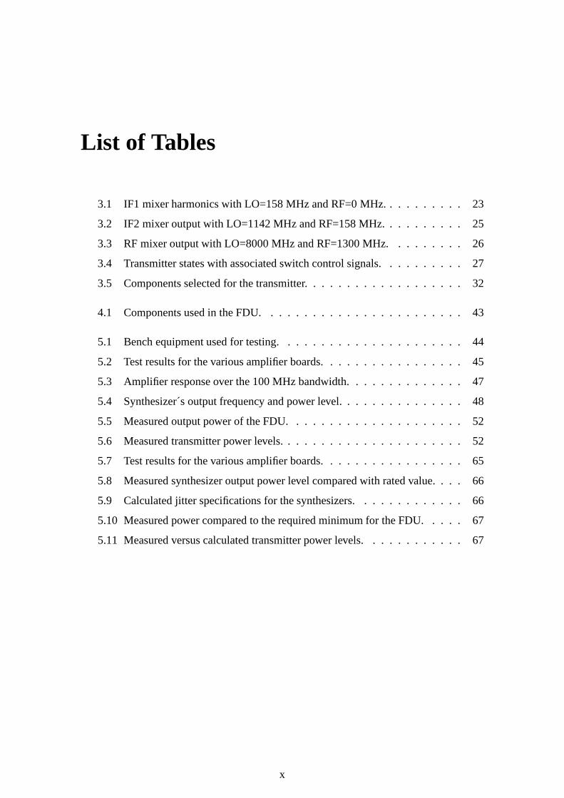
These two signals are respectively multiplied with a 158 MHzsine or cosine waveform
(irrespective of order). This is equivalent to upconversion with a common LO with one
arm being shifted by 90 degrees. Figs 3.3 and 3.4 are the result of these two operations.
15
−400 −300 −200 −100 0 100 200 300 4000
10
20
30
40
50
60
70
80
90
Frequency [MHz]
Mag
nitu
de
I Channel at 158MHz IF
Figure 3.3: I channel spectrum at 1st IF (Matlab simulation)
16

−400 −300 −200 −100 0 100 200 300 4000
10
20
30
40
50
60
70
80
Frequency [MHz]
Mag
nitu
de
Q Channel at 158MHz IF
Figure 3.4: Q channel spectrum at 1st IF (Matlab simulation)
They are then combined at this frequency to produce the complex signal:Chirp = (I +
jQ)IF . This has a bandwidth of 100 MHz. The Matlab code for these graphs is included
in Appendix A [7].
17

−400 −300 −200 −100 0 100 200 300 4000
10
20
30
40
50
60
70
80
90
Frequency [MHz]
Mag
nitu
de
Chirp at 158MHz IF
Figure 3.5: Chirp spectrum at 1st IF (Matlab simulation)
The setup, which appears in Fig. 3.6, simulates the above process with a time-domain
processor called Systemview (by Elanix). The two baseband channels are shifted up in
frequency by LO signals differing in phase by 90 degrees withidentical mixers. These two
158 MHz signals are then combined to produce the chirp signal. A 5th order Butterworth
filter is applied to the output.
18

Figure 3.6: Systemview setup for simulation of IF1.
The simulation results follow:
Figure 3.7: Time and frequency domain graphs of in-phase andquadrature chirp signalsat baseband.
19

Figure 3.8: Time and frequency domain graphs of in-phase andquadrature chirp signalsat 158 MHz (IF1).
20

Figure 3.9: Resultant complex chirp signal.
21

3.2 Mixers and Filters
Mixers are used to translate a signal in frequency (either upor down). The RF signal to be
translated is combined with a LO signal in a non-linear element such as a diode. It outputs
nLO±mRF, where m, n are integers or zero. These sums and differences are referred to as
the mixers harmonic intermodulation products. Common types are the unbalanced, singe
balanced, double balanced and image reject mixers. The important factors to consider are
minimum LO and maximum RF input power level, conversion loss, port-to-port isolation,
return loss and of course frequency.
For up-conversion in the SASAR2 transmitter, the upper sideband (LO+RF) is the only
desired output and all other signals need to be filtered out. The output of each of the
transmitter sections needs to be ascertained to ensure unwanted signals are attenuated
sufficiently before entering the successive stage. Essentially, this analysis details the re-
quired filter characteristics for each of the three up-conversion stages.
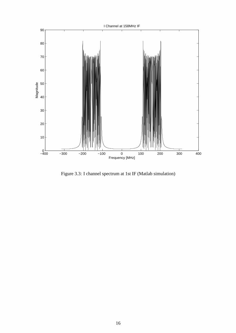
The three properties: bandwidth, steepness of the transition from passband to stopband
(roll-off) and delay time are of great interest in selectinga bandpass filter in a wideband
radar system. The degree at which a filter of defined bandwidth¨rolls off¨ is determined by
the number of poles it incorporates. However, delay time increases with an increase in the
number of poles and decreases with an increasing bandwidth.Therefore, a compromise
must be made. It is important to make the filter bandwidth reasonably larger than the
signal bandwidth as can be seen from Fig. 3.10. If this is not done, delay at the outer
frequency components will differ from those at the central frequency components of the
spectrum. This phenomenon is known as group delay and causesthe pulse envelope to
vary from input to output [2, 9]. This is undesirable as it compromises the resolution of
the SAR system. The user-requirements state that Butterworth filters are to be used. This
is because they incorporate the best trade-off between flatness in the passband, degree of
roll-off and flatness of time delay [11]. Since 5th order filters are to be used, the only
parameter that may be varied is the bandwidth.
22
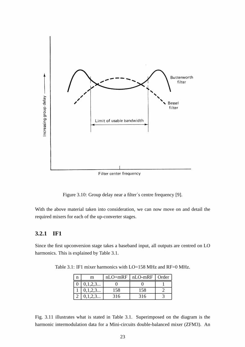
Figure 3.10: Group delay near a filter´s centre frequency [9].
With the above material taken into consideration, we can nowmove on and detail the
required mixers for each of the up-converter stages.
3.2.1 IF1
Since the first upconversion stage takes a baseband input, all outputs are centred on LO
harmonics. This is explained by Table 3.1.
Table 3.1: IF1 mixer harmonics with LO=158 MHz and RF=0 MHz.
n m nLO+mRF nLO-mRF Order
0 0,1,2,3... 0 0 11 0,1,2,3... 158 158 22 0,1,2,3... 316 316 3
Fig. 3.11 illustrates what is stated in Table 3.1. Superimposed on the diagram is the
harmonic intermodulation data for a Mini-circuits double-balanced mixer (ZFM3). An
23

ideal brick-wall bandpass filter centred at 158 MHz could have a maximum theoretical
passband of 216 MHz in order to ensure only LO+RF is presentedto the next mixer.
However, for a realistic filter, it is possible that signal feed-through (RF) and second
harmonic (2LO+RF) will not be attenuated below the noise floor. The darker dashed line
shows the 5th order Butterworth response, while the dotted line displaysits effect on the
spectrum. The effects of these adjacent signals entering the mixer of IF2 must therefore
be considered.
Figure 3.11: IF1 harmonic intermodulation (relative to desired IF output) for Mini-circuitsZFM3 mixer with filter attenuation.
3.2.2 IF2
Signal feed-through from the IF1 mixers would be translatedby this mixer to be centred at
1142 MHz (LO). The other signal that would possibly enter this mixer (2LO+RF) would
sit where this mixers LO+2RF sits (see Table 3.2). This is because the first stage was
mixing up from baseband and therefore, the LO frequency of the first stage is equal to
the RF input of the second stage. So, all harmonics of the firststage will mix up to sit
exactly where harmonics of the second stage sit. Therefore,the filter requirements for the
output of IF2 should be more stringent than for IF1. If the second filter is to remove its
harmonics, then the previous stages harmonics will also be removed here. This allows the
requirements of the first filter be relaxed.
24

Table 3.2: IF2 mixer output with LO=1142 MHz and RF=158 MHz.
n m nLO+mRF nLO-mRF Order
0 1 158 -158 11 0 1142 1142 11 1 1300 984 21 2 1458 826 31 3 1616 668 42 6 3232 1136 82 7 3390 978 9
Once again, mixer harmonic intermodulation data and the effect of filter attenuation is
shown in Fig. 3.12 for a Mini-circuits ZLW-5 double-balanced mixer. The image and LO
feed-through are found to be sufficiently large to warrant alarm bells.
Figure 3.12: IF2 harmonic intermodulation (relative to desired IF output) for Mini-circuitsZLW-5 mixer.
This problem can be vastly improved by replacing the double-balanced mixer with an
image rejection mixer. Therefore, a Miteq IR0102LC1C mixeris used here. This mixer
boasts image rejection of 23 dB and LO-RF isolation of 40 dB.
3.2.3 RF
Analysing this mixer, without giving attention to harmonics from the previous, gives rise
to Table 3.3 and Fig. 3.13.
25

Table 3.3: RF mixer output with LO=8000 MHz and RF=1300 MHz.
n m nLO+mRF nLO-mRF Order
0 1 1300 -1300 10 6 9100 -9100 60 7 10400 -10400 71 0 8000 8000 11 1 9300 6700 21 2 10600 5400 32 5 22500 9500 72 6 23800 8200 8
Figure 3.13: Third mixer harmonic intermodulation (relative to desired IF output). MiteqMO812M5
This stage has far less critical filtering requirements thanthe previous two. However,
if harmonics on either side of LO+RF from the previous stage are considered to be let
through, then the filters passband for the final mixer is reduced to that of the previous two
stages. This makes the role of the IF2 filter even more important. For this reason and
because the TWT has a narrow input frequency range, no filter is included here.
3.3 BIT
The output of each frequency stage is diverted through asingle pole double throw(SPDT)
switch to the equivalent section in the receiver. This is achieved by applying a TTL high
(+5 V) signal to the control input of the switch. The RCU shallperform this function.
Therefore, with no signal applied to the switches, the transmitter will perform its normal
function. Table 3.4 shows the states of this function. This verifies the design up to the
power amplifier input.
26

Table 3.4: Transmitter states with associated switch control signals.
IF1 switch IF2 switch RF switch Transmitter State
0 0 0 Transmit mode0 0 1 RF verification0 1 0 IF2 verification0 1 1 -1 0 0 IF1 verification1 0 1 -1 1 0 -1 1 1 -
A test function is now developed to confirm the operation of the TWT. This consists of a
directional coupler, transfer switch, dummy load and two power detectors (see Fig. 3.14).
The transfer switch with dummy load allow us to access full TWT power without the
inherent dangers of transmitting at this high power. This ispurely a testing facility. The
directional coupler has power detectors on both coupled arms to monitor forward and
reverse power. The transfer switch will be switched to dummyload to ensure correct
power levels and then back to transmit before transmission.It will then remain here
until power down. After peak level detection, the analogue values are sent to the RCU
for digitisation and interpretation. Power levels are still monitored during transmission,
however, and if boundary conditions are exceeded the TWT canbe shut down.
R1
DC1
D1 D2
S4 To DuplexerFrom PA
Figure 3.14: Diagram of the BIT.
27

Figure 3.15: Photo of the waveguide BIT components attachedto the duplexer.
3.4 Power Requirements of Proposed Transmitter
With a viable transmitter now realised, the power levels need to be tracked through the
system to ensure all components meet there input specifications. This analysis will deter-
mine where amplification/attenuation is required. Since the TWT output requires waveg-
28

uide transmission lines, analysis also needs to done to determine if they are capable of
handling the high power.
3.4.1 Power Levels
The Terms of Reference state that the DPG outputs two +10 dBm signals. This input
level requires a mixer with a very high LO power level. This will put pressure on the
FDU to attain this power specification. Therefore, these signals are attenuated in order
to deliver 0 dBm to each IF1 mixer. The proposed system is shown in Fig. 3.16. All
mixer specifications are stated below the component in the diagram. Losses for other
components are also shown. This diagram includes BIT components in the dotted boxes.
All connections are 50Ω, SMA female.
29

30

It must be realized though, that until components are put on the test bench and power
levels measured, values obtained from data sheets are merely estimates. They are the
estimated lowest values ie. worst case. Also, losses due to connecting cables have not
been taken into account. It is for this reason that, for all components where input power is
crucial, levels are overstated by at least 3-4 dB. This will ensure correct operation with the
use of barrel attenuators to pad levels down to specific numbers. The use of attenuators
also acts to reduce the effects of reflections in the system, which are padded down by
twice the attenuation value for a two way reflection path.
With this noted, and the fact that the TWT requires a +10 dBm input, two 20 dB amplifiers
are inserted at the RF output. This raises the power level from -21.0 dBm to +18.1 dBm.
3.4.2 Waveguide Power-carrying Capacity
The maximum power which may pass through a waveguide will depend on the maximum
electric field strength that can exist without breakdown . Experimental data on allowable
field strengths at ultra-high frequencies indicates a valueof 30 000 volts/cm applicable for
air-filled guides under standard sea-level pressure, temperature and humidity conditions.
With this maximum allowable field strength specified, the maximum power-carrying ca-
pacity of the waveguide can be specified as:
P = E2
max6.63 ∗ 10−4ab( λλg
)
wherea andb are in cm andP is in watts. Herea andb are the dimensions of a rectangular
waveguide operating in the TE10mode witha> b [12].
With λ = 3.226 cm,λg = 4.175 cm,a = 2.54 cm andb = 1.27 cm, we get:
P = 1.487 MW
This figure assumes sea-level conditions. However, with increasing altitude it is found
that the potential gradient at which breakdown occurs decreases because of the change in
atmospheric pressure. Taking this into account and assuming that Paschen’s law holds for
ultra-high frequencies and assumes a seasonal average air density, it can be seen that at
10 000 ft (platform height), the maximum power must be derated by fifty percent. This
gives a theoretical maximum power-carrying capacity:
P = 743.5 kW
Therefore, depending on pressurisation of the aircraft, the figure should sit somewhere
between these two values. This far exceeds the power rating of the TWT.
3.5 Summary
The theory of combining an in-phase and quadrature chirp signal was introduced. Through
simulation of this, the hardware of the first IF stage was initialised. Some mixer and filter
31

theory then lead into analysis of specified mixer harmonic intermodulation rejection. The
first filter was not deemed critical and its bandwidth is set to140 MHz. The second filters´
role was determined to be crucial and therefore its bandwidth is set to 120 MHz and the
double-balanced mixer was exchanged for an image rejectionmixer. The third filter had,
potentially, the least critical constraints. Because of the TWTs narrow input frequency
range it was thus excluded. A testing function was then outlined which sequentially mon-
itors the output of each frequency stage.
With the transmitter all but designed, a power budget was drawn up which introduced
the need for amplification. Analysis was done on the power-handling capability of the
waveguide used. It was found that power levels do not pose threat to the breakdown
of air. Table 3.5 summarises the components used in the transmitter. Fig. 3.16 can be
referred to for component name designation.
Table 3.5: Components selected for the transmitter.
Component name Manufacturer Part number
AMP1 Tellumat CustomAMP2 Tellumat CustomAMP3 - -
D1 Advanced Control ASCP2504PC3D2 Advanced Control ASCP2504PC3
DC1 Hewlett Packard X750EFL1 Lorch CustomFL2 Lorch CustomFL3 - -FL4 - -FL5 Lorch Custom
MIX1 Mini-circuits ZFM3MIX2 Mini-circuits ZFM3MIX3 Miteq IR0102LC1CMIX4 Miteq MO812M5
R1 Sperry 566S1 Sivers Lab 730 5X
SP1 Mini-circuits ZMSCQ-2-180SW1 Mini-circuits ZYSW-2-50RSW2 Mini-circuits ZYSW-2-50RSW3 Mini-circuits MSP2T-18
32
Chapter 4
Design and Implementation of
Frequency Distribution Unit
With the transmitter designed, it is now necessary to move tothe design of the FDU, which
will provide drive to the transmitter. As discussed in Section 2.5, a 10 MHz reference is
split and delivered to the various synthesizers. With this in mind, the synthesizers are
discussed and selected. The issue of power levels is then addressed with the intention of
specifying required amplification. Some theory follows which will enable the synthesizer
and amplifier hardware to be realised. A parameter whereby the performance of the FDU
outputs is measured is then discussed.
4.1 Frequency Synthesizers
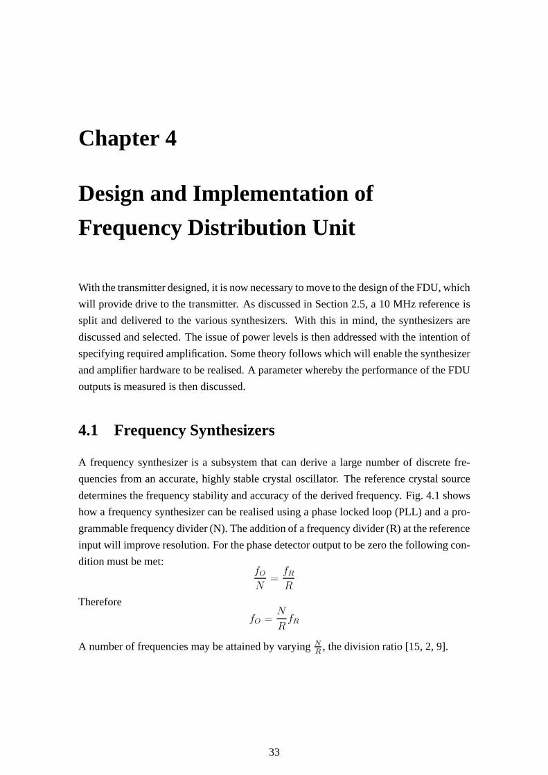
A frequency synthesizer is a subsystem that can derive a large number of discrete fre-
quencies from an accurate, highly stable crystal oscillator. The reference crystal source
determines the frequency stability and accuracy of the derived frequency. Fig. 4.1 shows
how a frequency synthesizer can be realised using a phase locked loop (PLL) and a pro-
grammable frequency divider (N). The addition of a frequency divider (R) at the reference
input will improve resolution. For the phase detector output to be zero the following con-
dition must be met:fO
N=
fR
R
Therefore
fO =N
RfR
A number of frequencies may be attained by varyingNR
, the division ratio [15, 2, 9].
33

Figure 4.1: Block diagram of a frequency synthesizer using aPLL and programmablefrequency synthesizers.
With the theory clear, the applicable synthesizers are chosen. They are the Synergy SPLL-
A40 (150-250 MHz), SPLH-S-A79 (1040-1185 MHz) and SPLH-4000F (4000 MHz).
Fig. 4.2 shows the configuration for the SPLH-S-A79. Only this particular synthesizer
will be explained owing to its similarity to the SPLL-A40. The SPLH-4000F is a fixed
frequency device and therefore does not require programming.
The external reference oscillator is divided down in the 14 bit reference divider and com-
pared to the VCO frequency which is divided by the 18 bit N counter. The error signal,
which is proportional to the phase difference between the two signals, is fed to a loop fil-
ter. This filter has been designed for maximum reference sideband rejection and optimum
acquisition speed.
Figure 4.2: Block diagram of the Synergy SPLH-S-A79 frequency synthesizer.
The synthesizer takes serial inputs on the Clock, Data and Latch Enable pins to program
the two counter dividers. The Clock input latches in a 19 bit word on the Data pin on the
rising edge of each pulse. If the Control bit (last bit input)is high, then data is transfered
to the R-counter and S Latch (prescalar select). If low, datais transfered to the N-counter.
The Latch Enable input goes high after each Control bit is input. National Semiconductors
Codeloader2 program[14] can be used to calculate the required outputs and program the
synthesizer. This is done via the parallel port of a computer.
The 4000 MHz output of the SPLH-4000F is doubled to achieve the required 8000 MHz
LO drive. This is done using the Mica F15KSP frequency doubler.
34

4.2 Power Issues
Once again, the power levels need examination to ensure outputs meet their requirement.
Fig. 4.3 illustrates the proposed FDU design, with necessary amplifiers included. As with
the transmitter, all connections are 50Ω, SMA female.
The 10 MHz reference outputs a 0 dBm signal. This is input to a Mini-circuits ZBSC-615
six way splitter which has a loss of -8.3 dBm. This poses the problem of not providing
sufficient input power for the frequency synthesizers (+6.0dBm). Therefore, an amplifier
is required to boost the power by at least 14.3 dB. This prompts the insertion of five
16 dB amplifiers. The extra gain is accounted for by reasons stated in Section 3.4.1. By
placing the amplifiers on the splitter output, instead of oneat the input, we achieve greater
isolation. This process is carried to the remaining three splitters.
The calculated power level is stated at the final outputs of Fig. 4.3. This is accompanied
by the minimum required power. All components have also beennamed for purposes of
clarity. A 50Ω termination is placed on the sixth output of SP3.
Figure 4.3: Diagram showing the proposed FDU design with predicted power levels.
4.3 Circuit Board Design
With the components of the FDU now set, the synthesizer chipsand surface mount am-
plifiers need to be placed on printed circuit board (PCB). To be consistent, input/output
impedances need to be maintained at 50Ω.
A transmission medium is required in order to transmit energy from one point to another.
Some kind of structure is needed if the medium is not air (in the case of RF/microwave
communication links). Traditionally, coaxial or waveguide technology has been used to
connect together prefabricated circuits and components inthe broad microwave range
from 0.1-30 GHz. More recently, microwave integrated circuits (MICs) have been de-
veloped where components are connected and manufactured using the same technology
but in a planar form. The conductor that replaces the coaxialline or waveguide is the
35

stripline [13, 16]. Although literature on the subject varies, this text will refer to the gen-
eral form of planar transmission line as stripline of which microstrip, slotline and coplanar
are sub-categories.
When it comes to planar transmission lines, the microstrip line is most common. Although
coplanar waveguide is widely viewed as better than microstrip for most applications, it too
has problems. To solve these problems, NASA Lewis and the University of Michigan de-
veloped a new version of the coplanar waveguide with electrically narrow ground planes.
They called this new transmission line thefinite ground coplanar waveguide(FGCW).
Through extensive numerical modelling and experimental measurements, they have char-
acterised the propagation constant of the FGCW, the lumped and distributed circuit el-
ements integrated in the FGCW and the coupling between parallel transmission lines.
Even though attenuation per unit length is higher for FGCW because of higher conductor
loss, it is comparable to conventional coplanar waveguide when the ground plane width
is twice that of the centre conductor (B = 2S) [18]. This structure is shown in Fig. 4.4.
Figure 4.4: Finite ground coplanar waveguide
The first task in designing any form of stripline is to select aboard material to suit the
intended frequency of operation. For each medium or guidingstructure there is an asso-
ciated permittivity. This quantity indicates how easily a material may be polarised and
is expressed asε = ε0εr. Hereε0 is the absolute constant for permittivity andεr is the
relative permittivity, also known as the dielectric constant, of the material used in the
MIC.
The second task is to calculate the line width for the intended characteristic impedance.
The impedance of a stripline is a function of the dielectric constant , the substrate height
h and the line width. As can be seen from Fig. 4.4, the analysisof line width is more
complex for FGCW than for that of microstrip. This is becausetwo strips of widthB do
not exist for microstrip. The reader is referred to [13] for adetailed analysis of impedance
calculation. Alternatively, many software options are available for simple calculation of
36

line widths. These range from simple java applets [21] on oneend of the spectrum to
complex programs, such as Polar Instruments Si6000 [22], onthe higher and more costly
side.
Using material withh = 1.524 mm, εr = 4.5 and line dimensionsS = W = 0.5 mm,
B = 1 mm produces the desired 50Ω line [21].
With the stripline taken care of, special care should be taken during board layout to min-
imise parasitics. This is particularly important at frequencies above 1 GHz. The following
steps should be adhered to during this process:
• Extra lead length corresponds to extra inductance added to the design. Therefore,
effort should be made to ensure components sit flush with transmission lines.
• Abrupt changes in transmission line width also cause parasitic effects called step
discontinuities. These can be reduced by tapering transmission lines down to the
component lead width.
• Parasitic effects can also be created by bends in a transmission line and hence this
should be avoided where possible. If not possible however, the corners should be
chamfered to prevent them from acting as extra shunt capacitance.
• Ground planes should be kept solid and as large as possible.
• High frequency return paths must be kept as short as possible. If plated through
holes are used as ground returns, they must be placed as near as possible to the
body of the package.
• Additional path length acts as series inductance and therefore transmission lines
must not be longer than they need to be.
With the FGCW line dimensions set and board guidelines laid out we can now move on
to implement the amplifier and frequency synthesizer boardsin order to realise the FDU.
4.4 Amplifiers
The amplifiers of the FDU up to 4 GHz are built using monolithicsurface mount
amplifiers. The circuit of Fig. 4.5 illustrates the biasing configuration and is obtained
from the data sheet of the particular amplifier. FGCW will connect the 50Ω components
between the RF input and output. These include two DC blocking capacitors and the
amplifier. The biasing resistor is calculated with a supply of +9 volts, and knowledge of
the biasing current. A RF choke of large impedance is inserted to combat the ¨power
divider¨ effect, where the bias resistor appears in parallel with the output load impedance.
37

Figure 4.5: Typical biasing configuration for Mini-circuits ERA amplifiers.
The boards are laid out using Protel and the the PCBs are acquired. The components are
then assembled and appropriate SMA connections are added. The boards are now realised
as shown in Figs. 4.6 and 4.7. The amplifiers connecting the the six way splitter to the
synthesizers are included on the synthesizer board to reduce the component count. All
boards are equipped with regulators to keep check on the supply voltage.
38

Figure 4.6: Realisation of board layout for the Mini-circuit´s ERA amplifiers.
Figure 4.7: Realisation of board layout for the Synergy frequency synthesizers.
39
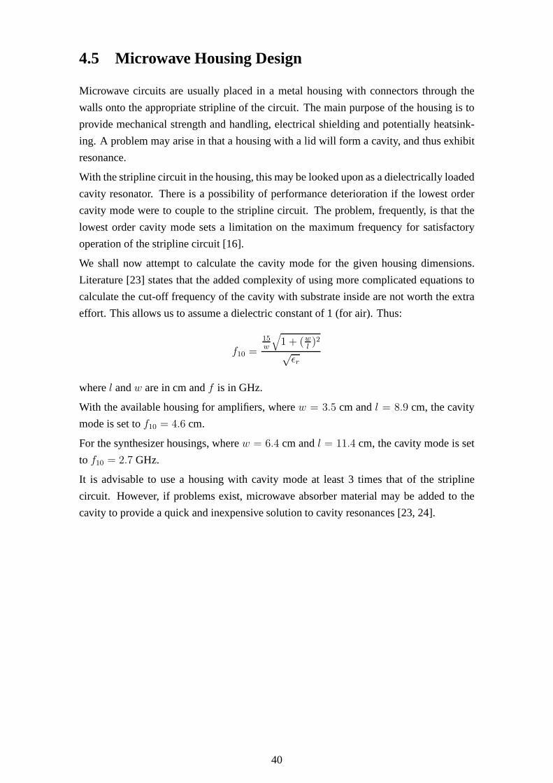
4.5 Microwave Housing Design
Microwave circuits are usually placed in a metal housing with connectors through the
walls onto the appropriate stripline of the circuit. The main purpose of the housing is to
provide mechanical strength and handling, electrical shielding and potentially heatsink-
ing. A problem may arise in that a housing with a lid will form acavity, and thus exhibit
resonance.
With the stripline circuit in the housing, this may be lookedupon as a dielectrically loaded
cavity resonator. There is a possibility of performance deterioration if the lowest order
cavity mode were to couple to the stripline circuit. The problem, frequently, is that the
lowest order cavity mode sets a limitation on the maximum frequency for satisfactory
operation of the stripline circuit [16].
We shall now attempt to calculate the cavity mode for the given housing dimensions.
Literature [23] states that the added complexity of using more complicated equations to
calculate the cut-off frequency of the cavity with substrate inside are not worth the extra
effort. This allows us to assume a dielectric constant of 1 (for air). Thus:
f10 =
15
w
√
1 + (wl)2
√εr
wherel andw are in cm andf is in GHz.
With the available housing for amplifiers, wherew = 3.5 cm andl = 8.9 cm, the cavity
mode is set tof10 = 4.6 cm.
For the synthesizer housings, wherew = 6.4 cm andl = 11.4 cm, the cavity mode is set
to f10 = 2.7 GHz.
It is advisable to use a housing with cavity mode at least 3 times that of the stripline
circuit. However, if problems exist, microwave absorber material may be added to the
cavity to provide a quick and inexpensive solution to cavityresonances [23, 24].
40

Figure 4.8: Completed module for the 158 MHz amplifiers (AMP11-2 and AMP11-3).
Figure 4.9: Completed module for the 150 MHz frequency synthesizer (SZ4).
4.6 Phase Noise and Jitter
Now that the FDU has been designed and implemented, a measureof the fidelity of the
produced signals must be established. This measure is termed phase noise in the fre-
41

quency domain or jitter in the time domain.
Phase noise is defined as the undesired phase variation of a signal. This is indicated by
the spreading of the frequency spectrum (s(t) = Asin(ωt + f(t))), as opposed to an
ideal signal (s(t) = Asin(ωt)) where the power is contained at one specific frequency. A
common measure of short-term frequency stability is the parameterL(fm), which refers
to theone-sided power spectral density of phase noise. As can be seen in Fig. 4.10,
L(fm) = N/C is the difference of power between the carrier atf0 and the noise atf0+fm.
The spectral distributions on either side of the carrier areknown as noise sidebands. The
units ofL(fm) are decibels below the carrier (dBc) per hertz .
Figure 4.10: Oscillator output power spectrum [15].
The bulk of oscillator noise close to the carrier is phase noise. This noise represents the
phase jitter or short-term stability of the oscillator. Jitter and phase noise are different
ways of quantifying the same phenomenon. The difference being that one is a time do-
main measurement, while the other is a frequency domain measurement [15, 19, 20].
4.7 Summary
Frequency synthesizers were discussed. It determined thatthey would provide an efficient
means of generating coherent signals for the clocks and LO drives. Synergy components
42

were selected. The FDU was attained by working power levels around the synthesizers
with knowledge of the reference output power. This detailedthe required amplifiers. A
breakdown of the components of the FDU appears below (see Fig. 4.3 for component
names):
Table 4.1: Components used in the FDU.
Component name Manufacturer Part number
AMP11-1 Mini-circuits ERA-50SMAMP11-2 Mini-circuits ERA-4SMAMP11-3 Mini-circuits ERA-4SMAMP12-1 Mini-circuits ERA-50SMAMP12-2 Mini-circuits ERA-2SMAMP12-3 Mini-circuits ERA-4SMAMP13-1 Mini-circuits ERA-50SMAMP13-2 Mini-circuits ERA-4SMAMP13-3 Tellumat CustomAMP13-4 Tellumat CustomAMP14-1 Mini-circuits ERA-50SMAMP15-1 Mini-circuits ERA-50SM
FD Mica F15KSPFL9 Lorch CustomSP3 Mini-circuits ZSBC-615SP4 Mini-circuits ZMSCQ-2-180SP5 Mini-circuits ZFSC-2-5SP6 Mini-circuits ZFSC-2-9-GSZ1 Synergy SPLL-S-A40SZ2 Synergy SPLH-S-A79SZ3 Synergy SPLH-4000FSZ4 Synergy SPLL-S-A40SZ5 Synergy SPLL-S-A40
Theory relevant to the design of RF PCBs was discussed and, with this knowledge, the
synthesizer and amplifier boards were constructed. They were housed in metal casings
which were analysed to determine if resonance will hinder the circuits performance. Phase
noise and jitter were introduced with the aim of understanding how to quantify the effec-
tiveness of the signals produced.
43

Chapter 5
Testing
5.1 Introduction
Testing of the transmitter and FDU is performed in order to verify the design. The fol-
lowing equipment is used:
Table 5.1: Bench equipment used for testing.
Equipment Model
DC power supply Topward 6303ADigital multimeter Escort EDM-2116LSpectrum analyzer Agilent E4407B (9kHz-26.5GHz)Sweep oscillator Hewlett Packard 8350B
Power meter Hewlett Packard HP 435AArbitrary waveform generator (AWG) Hewlett Packard 33120A
Where appropriate, similar FDU and transmitter componentsare tested together. How-
ever, the tests follow the general trend of FDU first, followed by transmitter. This results
from the necessity of using the FDU for various transmitter tests.
Thus, amplifiers are tested first (from both FDU and transmitter). The synthesizers are
then tested and a power budget for the FDU is drawn up. The firstIF is then tested with
the use of the FDU to inspect the integrity of the chirp signalproduced. A CW signal is
injected to the transmitter input with the aim of finalising the transmitter power budget.
A plot of the final chirp output spectrum is then compared to one of the the input to
establish the distortion of the signal´s magnitude throughthe system. The findings are
then discussed after all tests have been done and results shown.
44

5.2 Amplifier Testing
5.2.1 Equipment Used
DC power supply, power meter, sweep oscillator.
5.2.2 Test Procedure
The sweep oscillator is connected via a coaxial test cable tothe power meter. The sweep
oscillator is set to continuous wave (CW) mode and adjusted until the power meter reads
the desired input power level. The test cable is then disconnected and the FDU amplifier
boards are individually inserted with an attenuator equal to there gain. This process serves
to exclude losses outside the test circuit boundaries from the measurements and leave the
power meter settings unchanged. The DC supply is then attached to the amplifier and the
output is read off the power meter.
The procedure for the two transmitter amplifiers (Amps 1&2) is slightly different in that
the signal passed through them is of 100 MHz bandwidth. This requires the sweep oscil-
lator to be changed from CW to sweep mode. This is applied to the spectrum analyzer and
the hold maximum button is pushed to record the trace of the signal. A screen snapshot is
taken. Thereafter, the amplifier and an attenuator equal to the value of the amplifier gain
is inserted. This allows the spectrum analyzer settings to remain unchanged. The DC
supply is attached and the hold maximum button is pushed. A snapshot is again recorded.
5.2.3 Test Results
Table 5.2: Test results for the various amplifier boards.
Amplifier Frequency (MHz) Input (dBm) Output (dBm) Gain (dB) Expected Gain (dB)
Amp11-2 158 +2.0 +12.5 10.5 11.0Amp11-3 158 +2.0 +12.4 10.4 11.0Amp12-2 1142 0.0 +13.4 13.4 13.0Amp12-3 1142 0.0 +11.2 11.2 11.0Amp13-2 4000 +2.0 +13.0 11.0 11.0Amp13-3 8000 -2.0 +13.8 15.8 16.0Amp13-4 8000 -2.0 +13.8 15.8 16.0
Refer to Fig. 4.3 for the amplifier´s name designation.
45

Figure 5.1: Input to transmitter amplifier.
46

Figure 5.2: Output of transmitter amplifier with a 20 dB attenuation.
By subtracting Fig. 5.2 from Fig. 5.1, one can get an idea of how the amplifier maintains
its response over the frequency band of interest. This is shown in Table 5.3 below.
Table 5.3: Amplifier response over the 100 MHz bandwidth.
Frequency (GHz) 8.8 8.9 9.0 9.1 9.2 9.3 9.4 9.5 9.6 9.7 9.8
Amplitude (dB) 0.4 0.6 0.6 0.3 0.1 0.1 0.2 0.4 0.6 0.7 0.7
5.3 Synthesizer Testing
5.3.1 Equipment Used
DC power supply, spectrum analyzer, arbitrary waveform generator (AWG).
47

5.3.2 Test Procedure
The frequency and power level of each synthesizer is ascertained by the following pro-
cess: the AWG is set to 10 MHz at +4 dBm. The synthesizer outputis connected to the
spectrum analyzer and the power is supplied. The serial bit stream is then transferred from
Codeloader2 for the synthesizer of concern. The frequency and power level is recorded.
In order to obtain a phase noise plot, the spectrum analyzer must be changed to phase
noise mode. The carrier frequency and start (10 Hz) and stop (1 MHz) points must be
input. This results in a plot being generated.
5.3.3 Test Results
Table 5.4: Synthesizer´s output frequency and power level.
Synthesizer nameFrequency (MHz) Output (dBm) Expected Output (dBm)
SZ1 157.999 +5.42 +5.0SZ2 1141.999 +4.70 +5.0SZ3 3999.998 +3.08 +3.0SZ4 149.999 +5.27 +5.0SZ5 209.999 +5.43 +5.0
The graphs of each synthesizer output spectrum are displayed in Appendix B. These phase
noise plots follow:
48

Figure 5.3: Phase noise plot for the 158 MHz synthesizer.
Figure 5.4: Phase noise plot for the 1142 MHz synthesizer.
49

Figure 5.5: Phase noise plot for the 4000 MHz synthesizer.
Figure 5.6: Phase noise plot for the 150 MHz synthesizer.
50

Figure 5.7: Phase noise plot for the 210 MHz synthesizer.
5.4 Power Levels of the FDU
5.4.1 Equipment Used
DC power supply, power meter, AWG.
5.4.2 Test Procedure
The AWG is set to 10 MHz at +13 dBm and applied to the splitter input. This ensures both
arms receive the required +10dBm. The FDU (see Fig. 4.3) is then inserted and the DC
supply attached. The synthesizers are programmed and the output of each arm is applied
to and read off the power meter.
51

5.4.3 Test Results
Table 5.5: Measured output power of the FDU.
Arm frequency (MHz) Output Power (dBm) Calculated Output (dBm)
158 I +12.5 +12.7Q +12.4 +12.7
1142 T +14.4 +12.2R +12.2 +10.2
4000 T +12.1 +13.8R +12.1 +13.8
150 - +5.27 +5.0210 - +5.43 +5.0
5.5 Power Levels of the Transmitter
5.5.1 Equipment Used
DC power supply, power meter, sweep oscillator, AWG.
5.5.2 Test Procedure
The sweep oscillator is connected via a coaxial test cable tothe power meter. The sweep
oscillator (in CW mode) is then adjusted to the correct powerlevel. The first IF section
is then inserted (with appropriate FDU LO) and the DC supply attached and synthesizer
programmed. The power is then read off the power meter. This process is repeated with
IF2 added, and again with RF (the whole transmitter). The final two RF amplifiers are not
included.
5.5.3 Test Results
Table 5.6: Measured transmitter power levels.
Input Power (dBm) IF1 Power (dBm) IF2 Power (dBm) RF Power (dBm)
0dBm +1.1 -9.2 -17.1
5.6 Chirp Integrity
5.6.1 Equipment Used
DC power supply, spectrum analyzer, sweep oscillator, AWG.
52

5.6.2 Test Procedure
Each DPG output is connected successively to the spectrum analyzer and recorded. They
are then, along with the the two LO signals from the FDU, connected to the IF1 mixers.
Power is applied to the 158 MHz synthesizer and amplifiers. The programming data is
then sent to the synthesizer. The spectrum analyzer is attached to the IF1 filter output and
a trace is recorded. This process is repeated with IF2 added,then again with the addition
of RF.
5.6.3 Test Results
Figure 5.8: Spectrum of baseband in-phase chirp.
53
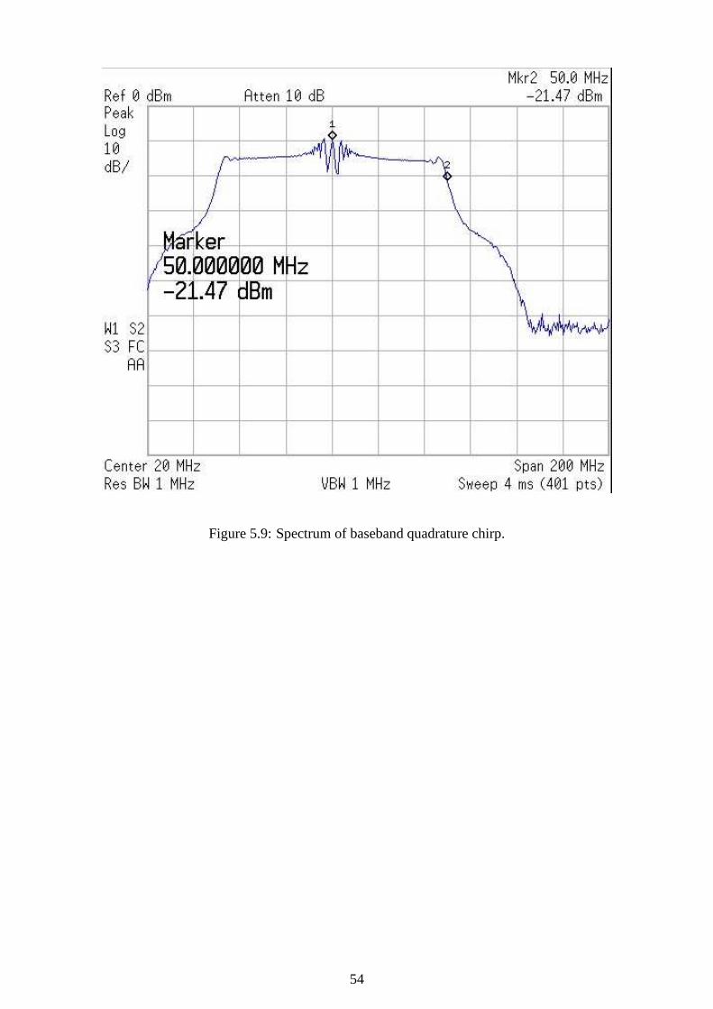
Figure 5.9: Spectrum of baseband quadrature chirp.
54

Figure 5.10: Spectrum of 158 MHz chirp.
55

Figure 5.11: Spectrum of 1300 MHz chirp.
56

Figure 5.12: Spectrum of 9300 MHz chirp.
5.7 Spurious Signals
5.7.1 Equipment Used
DC power supply, spectrum analyzer, AWG.
5.7.2 Test Procedure
The first IF section is connected (with appropriate FDU LO) and DC supply attached. The
synthesizer is programmed and the DPG applied to the input. The video and resolution
bandwidths are reduced to 3 kHz on spectrum analyzer. The resultant chirp signal is then
recorded. The chirp signal is turned off with the DPG still attached and another trace is
plotted. This process is repeated with IF2 added, and again with RF (the whole transmitter
and FDU).
57
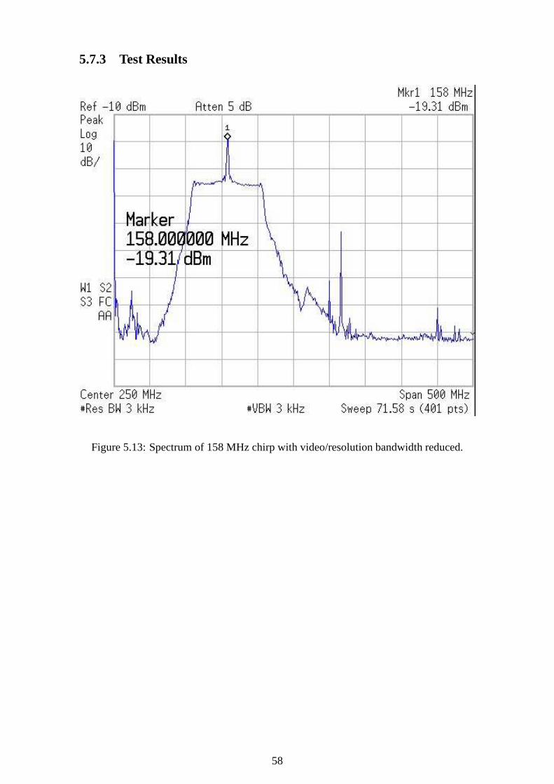
5.7.3 Test Results
Figure 5.13: Spectrum of 158 MHz chirp with video/resolution bandwidth reduced.
58

Figure 5.14: Spectrum without the presence of the 158 MHz chirp.
59

Figure 5.15: Spectrum of 1300 MHz chirp with video/resolution bandwidth reduced.
60

Figure 5.16: Spectrum without the presence of the 1300 MHz chirp.
61

Figure 5.17: Spectrum of 9300 MHz chirp with video/resolution bandwidth reduced.
62

Figure 5.18: Spectrum without the presence of the 9300 MHz chirp.
5.8 System Transfer Function
5.8.1 Equipment Used
DC power supply, spectrum analyzer, AWG.
5.8.2 Test Procedure
The first IF section is connected (with appropriate FDU LO) and DC supply attached. The
synthesizer is programmed and the DPG applied to the input. The resultant chirp signal
is then recorded on the spectrum analyzer. The entire systemis then inserted and relevant
DC supply attached and synthesizers programmed. A record ismade of the X-band chirp
on the spectrum analyzer.
63

5.8.3 Test Results
Figure 5.19: Spectrum of 158 MHz chirp.
64

Figure 5.20: Spectrum of 9300 MHz chirp.
5.9 Discussion and Analysis of Findings
5.9.1 Amplifier Testing
The table below shows the measured and rated gain of the FDU amplifiers.
Table 5.7: Test results for the various amplifier boards.
Amplifier name Frequency (MHz) Measured Gain (dB) Rated Gain (dB)
Amp11-2 158 10.5 11.0Amp11-3 158 10.4 11.0Amp12-2 1142 13.4 13.0Amp12-3 1142 11.2 11.0Amp13-2 4000 11.0 11.0Amp13-3 8000 15.8 16.0Amp13-4 8000 15.8 16.0
On the whole, the FDU amplifiers realise there rating withoutmuch deviation. It is also
65

seen that the transmitter amplifier does not deviate by more than 0.7 dB in terms of mag-
nitude linearity over the system bandwidth.
5.9.2 Synthesizer Testing
All the five synthesizers generated their required frequency with error less than 2 kHz.
Table 5.8 shows that their power specifications are also met.
Table 5.8: Measured synthesizer output power level compared with rated value.
Synthesizer name/frequency (MHz)Measured Output (dBm) Rated Output (dBm)
SZ1/158 +5.42 +5.0±2SZ2/1142 +4.70 +3.0 (min)SZ3/4000 +3.08 +3.0±2SZ4/150 +5.27 +5.0±2SZ5/210 +5.43 +5.0±2
.
The output frequency should reflect the reference frequencywithin the loop bandwidth.
Outside the loop bandwidth, the properties of the oscillator itself dominate. The step size
and noise of associated circuitry also contribute.
An applet by Raltron Electronics Corporation [20] is used toconvert the phase noise plots
to jitter values. These are stated in the Table 5.9 below.
Table 5.9: Calculated jitter specifications for the synthesizers.
Synthesizer name/frequency (MHz)Jitter (ps)
SZ1/158 11.1SZ2/1142 2.86SZ3/4000 2.15SZ4/150 12.7SZ5/210 10.4
What must be realised here is that the intended reference oscillator was not available at
the time of testing. The phase noise plots were produced using the AWG as the reference.
Therefore, these results are not a true reflection of the finalsystem. They are, however,
included to give an indication of the jitter. The 150 and 210 MHz synthesizer jitter values
are crucial as stated in the Terms of Reference (Section 1.1). Since the GPS crystal oscil-
lator is known to be superior in terms of stability, these values show promise, as they are
not too far off the required 6 ps.
66

5.9.3 Power Levels of the FDU
The power levels at the FDU outputs are compared to those needed at clock and mixer LO
inputs in Table 5.10. All levels exceed those required. The 158 MHz arm may be padded
down with a 6 dB attenuator, while a 3 dB attenuator will suffice for the receive side of
the 1142 MHz arm.
Table 5.10: Measured power compared to the required minimumfor the FDU.
Arm frequency (MHz) Final Output (dBm) Minimum Required Power (dBm)
158 I +13.7 +7.0Q +13.6 +7.0
1142 T +12.2 +10.0R +12.6 +7.0
4000 T +12.1 +8.0R +12.1 +8.0
150 - +5.27 +4.0210 - +5.43 +4.0
5.9.4 Power Levels of the Transmitter
The transmit power budget, Table 5.11, confirms the calculated power levels of the Fig 3.16.
The test cables and connectors will account for the additional losses . With the addition of
the transmitter amplification, the power will rise to 16.5 dBm. A 6 dB attenuator can then
bring this down to the required +10 dBm. Alternatively, the amplification on the DPG
outputs can can adjusted accordingly.
Table 5.11: Measured versus calculated transmitter power levels.
Input Power (dBm) IF1 Power (dBm) IF2 Power (dBm) RF Power (dBm)
Measured 0 -6.6 -16.8 -23.5Calculated 0 -6.1 -15.2 -21.9
5.9.5 Chirp Integrity
The chirp signal delivered by the DPG is of satisfactory quality. However, the power level
is approximately 25 dB below that stated in the Terms of Reference and 15 dB below
what the transmitter input can tolerate. It will therefore need amplification in order for
the TWT to receive its intended power requirement.
Combination of the I and Q baseband signals is achieved by theprocess detailed in Section
3.1. There is evidence of LO feedthrough from the two 158 MHz mixers. The chirp seen
67

at the second IF (Fig. 5.11) shows evidence of attenuation atthe outer frequencies. This
has resulted from the filter bandwidth (120 MHz) not being large enough to combat the
effects of group delay. This is carried through to the RF signal, which does not suffer the
same fate.
5.9.6 Spurious Signals
With the video/resolution bandwidths decreased, the noisefloor drops accordingly. This
results in the unmasking of previously unseen frequency components, much like sprouting
grey hairs. Fig. 5.13 shows the LO feedthrough and 316 MHz LO harmonic clearly.
Without the chirp present in Fig. 5.14 things are less clear.The only possible source of
these signals would be the DPG, since the LO has been characterised.
The LO harmonic of the previous stage disappears in the 1300 MHz spectrum. The
1142 MHz LO feedthrough still exists though, despite the efforts of the image rejec-
tion mixer. Its effort, together with the filter concerned, do provide in excess of 80 dB
isolation. The image, however, is attenuated below the noise floor. The presence of the
two spikes offset by 16 MHz from the 1300 MHz signal is a resultof the previous stage.
Once again, this trend continues through to the X-band spectrum. As would be expected,
due to the lack of a filter, harmonics at 8000 MHz spacings exist. It must be noted that the
video and resolution bandwidths were increased in Fig. 5.18to cover the the 5000 MHz
span.
5.9.7 System Transfer Function
Fig. 5.21 indicates how the chirp envelope varies from IF1 output to RF output.
Figure 5.21: System transfer function.
68

Chapter 6
Conclusions and Recommendations
6.1 Conclusions
In view of the findings, the following conclusions may be drawn:
• All the FDU amplifiers provide sufficient gain for their application.
• The synthesizers output their desired frequency at sufficient power level.
• It is not clear if the jitter specification of 6 ps has been met,although it does seem
promising.
• The FDU supplies sufficient power at all of its outputs.
• The DPG was found to be lacking of 24 dB. Transmitter power levels will supply
the desired +10 dBm to the TWT if this is corrected for.
• Combination of the in-phase and quadrature chirp signals isdone satisfactorily. LO
feedthrough, however, is superimposed at the chirps´ centre frequency.
• As a result of previous stages spurious signals exist at 16 MHz offset from the
chirps´ centre frequency and at 9142 MHz. Harmonic intermodulation products of
the final mixer are also present.
• The system transfer function reveals that 2 dB attenuation is present at the outer
frequencies of the chirp signal. Group delay in the filters and transmitter amplifiers
is held responsible for this.
69

6.2 Recommendations for Future Work
As a result of the findings and conclusions, the following recommendations are made:
• The frequency synthesizers´ jitter specification should becalculated when the GPS
reference is acquired.
• Amplification of at least 15 dB must be performed to the DPGs´ outputs.
• The IF1 mixers could be replaced with higher demands on LO-RFisolation.
• Analysis may be done to determine the origin of the 16 MHz offset spurious re-
sponses.
• The TWT must be inserted to test the need for X-band filtering.
70

Appendix A
Matlab Chirp Simulation Code
Fs = 630e6; % Sample Rate
Tp = 5e-6; % Chirp pulse length in seconds
ChirpBW = 100e6; % Chirp Bandwidth
NumSamples = round(Fs * Tp);
I = zeros(1,NumSamples);
Q = zeros(1,NumSamples);
Tplot = zeros(1,NumSamples);
TimePerSample = 1/Fs;
Gamma = ChirpBW/Tp;
%%%%%%% Create Chirp %%%%%%%%%%%%
for count = 0:(NumSamples-1)
Time = (TimePerSample*count-(Tp/2));
Phase = pi * Gamma * Time^2;
I(1,count+1) = cos(Phase);
Q(1,count+1) = sin(Phase);
Tplot(1,count+1) = (Time+(Tp/2));
end
%%%%%%%% Take FFT of chirp %%%%%%
Chirp = complex(I,Q);
ChirpFFT = fft(Chirp);
%%%%%%%% modulation section%%%%%%%%
Fcarrier = 157.5e6; % Modulation Frequency
N = 10; % Number of address bits
dF = Fs * 2^(-N); % Frequency resolution
FCN = round(Fcarrier/dF); % Frequency Control Number
NCOSin = zeros(1,NumSamples);
NCOCos = zeros(1,NumSamples);
for count = 1:NumSamples
NCOCos(count) = cos(2*pi*(mod(count*FCN,2^N))/2^N);
NCOSin(count) = sin(2*pi*(mod(count*FCN,2^N))/2^N);
end
IMod = NCOCos.*I;
QMod = NCOSin.*Q;
FIMod = fft(IMod);
FQMod = fft(QMod);
ChirpMod = IMod + QMod;
ChirpModFFT = fft(ChirpMod);
NCOSinFFT = fft(NCOSin);
%%%%%%%%% Shift FFT %%%%%%%%%%%%
ChirpModFFT = fftshift(ChirpModFFT);
NCOSinFFT = fftshift(NCOSinFFT);
ChirpFFT = fftshift(ChirpFFT);
71
%%%%%%%%% plot graphs %%%%%%%%%%%%
step = Fs/(NumSamples*1e6);
x = -Fs/(2*1e6):step:Fs/(2*1e6)-step;
figure,plot(x,abs(FIMod))
xlabel(’Frequency [MHz]’)
ylabel(’Magnitude’)
title(’I Channel at 158MHz IF’);
figure,plot(x,abs(FQMod))
xlabel(’Frequency [MHz]’)
ylabel(’Magnitude’)
title(’Q Channel at 158MHz IF’);
figure,plot(x,abs(ChirpModFFT))
xlabel(’Frequency [MHz]’)
ylabel(’Magnitude’)
title(’Chirp at 158MHz IF’);
figure,plot(x,abs(NCOSinFFT))
xlabel(’Frequency [MHz]’)
ylabel(’Magnitude’)
title(’158MHz sinusoid’)
figure,plot((Tplot/1e-6),I);
xlabel(’Time [us]’)
ylabel(’Magnitude’)
title(’I Channel’)
figure,plot((Tplot/1e-6),Q);
xlabel(’Time [us]’)
ylabel(’Magnitude’)
title(’Q Channel’)
end
end
72
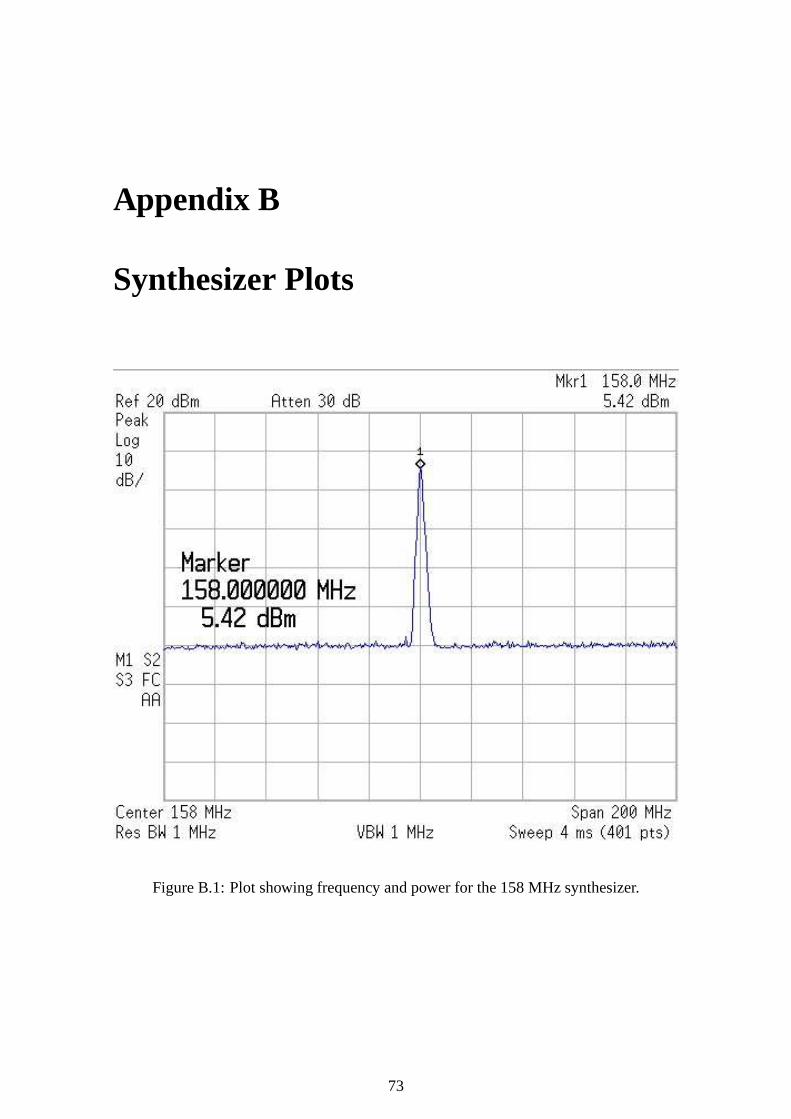
Appendix B
Synthesizer Plots
Figure B.1: Plot showing frequency and power for the 158 MHz synthesizer.
73

Figure B.2: Plot showing harmonics of the 158 MHz synthesizer.
74

Figure B.3: Plot showing frequency and power for the 1142 MHzsynthesizer.
75

Figure B.4: Plot showing harmonics of the 1142 MHz synthesizer.
76

Figure B.5: Plot showing frequency and power for the 4000 MHzsynthesizer.
77

Figure B.6: Plot showing harmonics of the 4000 MHz synthesizer.
78

Figure B.7: Plot showing frequency and power for the 150 MHz synthesizer.
79

Figure B.8: Plot showing harmonics of the 150 MHz synthesizer.
80

Figure B.9: Plot showing frequency and power for the 210 MHz synthesizer.
81

Figure B.10: Plot showing harmonics of the 210 MHz synthesizer.
82

Bibliography
[1] S. Kingsley and S. Quegan, “Understanding Radar Systems”, Scitech Publishing,
Inc, 1999.
[2] Donald R. Wehner, “High-Resolution Radar”, 2nd EditionArtech House, 1994.
[3] M. Jacobs, Correspondance, e-mail.
[4] A. Wilkinson, Radar Signal Processing Course notes, UCT, 2002.
[5] M. R. Inggs, “SASAR II Subsystem User Requirements”, UCTTechnical report,
February 2003.
[6] R.T. Lord, M. R. Inggs, “SASAR II Design Document”, UCT Technical report,
2003.
[7] R.T. Lord, “SASAR II Digital Aquistition System Simulation Results”, UCT Tech-
nical report, Doc: rrsg:3895, 2004.
[8] M. Skolnik, “Radar Handbook”, 2nd Edition, McGraw-Hil,Inc, 1990.
[9] Ronald C. Stirling, “Microwave Frequency Synthesizers”, Prentice Hall, Inc, 1987.
[10] F. G. Stremler, “Introduction to Communication System”, Addison Wesley Publish-
ing Company, Inc.
[11] Horrowitz and Hill, “The Art of Electronics”, 2nd Edition, Cambridge University
Press, 1991.
[12] Theodore Moreno, “Microwave Transmission Design Data”, Artech House, 1989.
[13] Renuit K. Hoffmann, “Handbook of Microwave IntegratedCircuits”, Artech House,
1987.
[14] http://www.national.com/appinfo/wireless/0,1822,185,00.html
[15] Kai Chang, “RF and Microwave Wireless Systems”, John Wiley & Sons, 2000.
[16] L. A. Trinogga, Guo Kaizhou, I. C. Hunter, “Practical Microstrip Circuit Design”,
Ellis Horwood Limited, 1991.
83

[17] Barry Downing, UCT EEE482F course notes, UCT, 2002.
[18] G. E. Ponchak,http://privatewww.essex.ac.uk/~bolat/coplanarwaveguide.html
[19] http://www.radiolab.com.au/DesignFile/PNRefPNRef.htm
[20] Neil Roberts, “Phase Noise and Jitter- A Primer for Digital Designers”,
http://timing.zarlink.com/assets/Phase_Noise_and_Jitter_Article.pdf,2003
[21] Hao Shi,http://www.eecircle.com/applets/016/Gcp3.html,2001.
[22] http://www.polarinstruments.com
[23] http://www.triquint.com/company/divisions/millimeter_wave/DesignGuidelinesApNote.pdf
[24] http://www.eccosorb.com/cavity_resonance.asp
[25] M. Skolnik, “Introduction to radar systems”, 2nd Edition, McGraw-Hil, Inc.
[26] H. Krauss et al, “Solid State Radio Engineering”, John Wiley & sons, 1980.
[27] Doug DeMaw, “Practical RF Design Manual”, Prentice Hall, Inc, 1982.
[28] Joeseph J. Carr, “RF Components and Circuits”, Elsevier Science, 2002.
[29] Norman Morrison, “Introduction to Fourier Analysis”,John Wiley & sons, 1994.
[30] S. A. Hovanessian, “Radar System Design and Analysis”,Artech House, 1984.
[31] A. S. Gilmour, “Principles of Travelling Wave Tubes”, Artech House, 1994.
[32] Dean L. Mensa, “High Resolution Radar Cross-Section Imaging”, Artech House,
1991.
[33] Barton et al, “Radar Evaluation Handbook”, ANRO Engineering, Inc, 1991.
[34] Charles Elachi, “Introduction to the Physics and Techniques of Remote Sensing”,
John Wiley & sons, 1987.
[35] V. Mannassewitsch, “Frequency Synthesizers Theory and Design”, John Wiley &
sons, 1976.
84


![FPGA-Based Implementation of IEEE 802.16d WiMAX …... thus Implementation design ... has implemented an OFDM transmitter on Altera Statix II FPGA ... [17], Implemented OFDM transmitter](https://img.pdfslide.us/doc/110x75/5acf24d37f8b9a8b1e8c527c/fpga-based-implementation-of-ieee-80216d-wimax-thus-implementation-design.jpg)