Embed Size (px)
Citation preview

Design and implementationof a multi-channelspace-borne SAR imagingsystem on Vivado HLS
Zixin Gao, Chen Yang, Yizhuang Xiea), Bingyi Li, He Chen,and Yu XieBeijing Key Laboratory of Embedded Real-time Information Processing Technology,
Beijing Institute of Technology, Beijing 100081, China
Abstract: New generation space-borne SAR (synthetic aperture radar)
systems require high real-time processing performance and have size, weight
and power constrains. This paper presents a multi-channel stripmap SAR
imaging system implemented on an FPGA platform. In order to reduce
FPGA design cost, a high-level synthesis tool Xilinx Vivado HLS is applied
to design and implement the SAR imaging system. FFT algorithms in the
imaging algorithm use FFT IP cores in FPGA, and the rest is customized on
HLS. The modules designed on HLS are optimized and packaged as IP
blocks for FPGA implementation of the imaging system. The performance
and resource utilization of the whole system are evaluated by processing a
two-channel SAR raw data with a granularity of 16384 × 4096. The system
can complete imaging in about 4.7 s at 100MHz operating frequency.
Keywords: multi-channel SAR, FPGA, HLS, implementation
Classification: Integrated circuits
References
[1] N. Gebert and G. Krieger: “Azimuth phase center adaptation on transmit forhigh-resolution wide-swath SAR imaging,” IEEE Geosci. Remote Sens. Lett. 6(2009) 782 (DOI: 10.1109/LGRS.2009.2025245).
[2] J. J. Xiong, et al.: “The FPGA design of on board SAR real time imagingprocessor,” Acta Electronica Sinica 33 (2005) 1070 (DOI: 10.3321/j.issn:0372-2112.2005.06.027).
[3] M. Bian, et al.: “High-performance system design of SAR real-time signalprocessing,” IEEE International Conference on Computer Application andSystem Modeling (2010) V12-126 (DOI: 10.1109/ICCASM.2010.5622137).
[4] D. O’Loughlin, et al.: “Xilinx Vivado high level synthesis: Case studies,” IETIrish Signals & Systems Conference 2014 and 2014 China-Ireland InternationalConference on Information and Communications Technologies (2014) 352(DOI: 10.1049/cp.2014.0713).
[5] J. Cong, et al.: “High-level synthesis for FPGAs: From prototyping todeployment,” IEEE Trans. Comput.-Aided Des. Integr. Circuits Syst. 30 (2011)473 (DOI: 10.1109/TCAD.2011.2110592).
[6] Y. Guo, et al.: “Rapid industrial prototyping and SoC design of 3G/4G wireless
© IEICE 2018DOI: 10.1587/elex.15.20180254Received March 9, 2018Accepted March 22, 2018Publicized April 4, 2018Copyedited May 25, 2018
1
LETTER IEICE Electronics Express, Vol.15, No.10, 1–12

systems using an HLS methodology,” EURASIP J. Embed. Syst. 2006 (2006)18 (DOI: 10.1155/ES/2006/14952).
[7] Z. Jia, et al.: “Relative radiometric correction for remote sensing images basedon VIVADO HLS,” IET International Radar Conference 2015 (2016) 4 (DOI:10.1049/cp.2015.1439).
[8] A. Currie and M. A. Brown: “Wide-swath SAR,” IEE Proc. F Radar SignalProcess. 139 (1992) 122 (DOI: 10.1049/ip-f-2.1992.0016).
[9] J. Brown: “Multi-channel sampling of low-pass signals,” IEEE Trans. CircuitsSyst. 28 (1981) 101 (DOI: 10.1109/TCS.1981.1084954).
[10] Ding.: “Data processing of multi-channel space-borne SAR,” 551 (2009) 1(DOI: 10.1049/cp.2009.0449).
[11] R. K. Raney, et al.: “Precision SAR processing using chirp scaling,” IEEETrans. Geosci. Remote Sens. 32 (1994) 786 (DOI: 10.1109/36.298008).
[12] C. Yang, et al.: “A spaceborne synthetic aperture radar partial fixed-pointimaging system using a field-programmable gate array—Application-specificintegrated circuit hybrid heterogeneous parallel acceleration technique,”Sensors 17 (2017) 1493 (DOI: 10.3390/s17071493).
[13] H. Tang, et al.: “A spaceborne sar on-board processing simulator using mobilegpu,” Geoscience and Remote Sensing Symposium (IGARSS) (2016) 1198(DOI: 10.1109/IGARSS.2016.7729303).
[14] N. M. Desai, et al.: “Near real time SAR processors for ISRO’s multi-modeRISAT-I and DMSAR,” European Conference on Synthetic Aperture Radar(2008) 1.
1 Introduction
Space-borne Synthetic Aperture Radar (SAR) is an active microwave remote
sensing device with all-day, all-weather features in earth observation and has been
widely used in military and civilian areas. Traditional space-borne SAR can not
meet higher and higher index requirements due to azimuth ambiguities and range
ambiguities. Azimuth multi-channel technology is a major technical way to achieve
wide swath with high azimuth resolution, and it is a hot research topic of the new
generation space-borne SAR systems [1]. At present, there are three main types of
technologies for implementing real-time SAR processing: large-scale Field Pro-
grammable Gate Array (FPGA) technology, ASIC technology and DSP technology.
However, in the case of on-orbit processing, an FPGA or an ASIC design is more
suitable for special environments of satellites due to the harsh constraints of the
severe size, weight, and power consumptions of the realization platform. FPGA and
ASIC both have a powerful parallel signal processing capability. However, com-
pared with an ASIC design, a design on an FPGA has excellent flexibility and cost-
effective that makes it prominent in space-borne SAR imaging systems. In [2], the
classical Chirp Scaling (CS) imaging algorithm is completed with seven FPGAs.
The system takes about 33 s to complete imaging with a granularity of 16384 �16384 at the operating frequency of 100MHz. Ming-ming Bian [3] uses FPGA to
complete the Range Doppler (RD) imaging algorithm.
At present, the most fundamental method of creating hardware design for
FPGA is by using hardware description languages Verilog or VHDL. And complex
timing state machine design is generally used for development within the FPGA,
© IEICE 2018DOI: 10.1587/elex.15.20180254Received March 9, 2018Accepted March 22, 2018Publicized April 4, 2018Copyedited May 25, 2018
2
IEICE Electronics Express, Vol.15, No.10, 1–12
which takes a lot of time to analyze and design. In order to get a better timing
performance, the simulation and optimization are repeated which take more time.
So if there is a tool that can be used to develop FPGA in C or C++ language, it will
bring more efficiency to FPGA design. The Xilinx Vivado High-Level Synthesis
(HLS) [4] tool can transform a C specification into register transfer level (RTL)
implementation, and we can export RTL out as IP which can be used in Xilinx
FPGA. C specifications can be written in C, C++, or SystemC language. Since we
can develop algorithms at the C-level and verify them at the C-level, it greatly
simplifies the design and debugging process, reduces the difficulty of development,
and greatly improves the efficiency of FPGA development. The design can be
modified according to the requirements and it is with high flexibility. In [5], the
effectiveness of state-of-art C-to-FPGA synthesis solutions targeting multiple
application domains is demonstrated, and the design productivity is improved.
The 3G/4G wireless systems using an HLS methodology is mentioned in [6],
which is with significantly improved productivity. In [7], the HLS tool is used to
design the relative radiometric correction of remote sensing image, which verifies
the high efficiency of developing FPGA based on HLS.
Considering the complexity of SAR imaging algorithm and the difficulty of
developing FPGA with hardware description languages, a Vivado HLS tool is
applied to design and implement a multi-channel stripmap SAR imaging system on
an FPGA platform in this paper. And the imaging system is evaluated from aspects
of image quality, system performance and resource utilization.
2 Multi-channel stripmap SAR algorithm
Multi-channel SAR imaging is based on a single transmitter for transmitting beam,
and multiple receivers for receiving the beam. The multi-receiver beam reception
mechanism enables wide swath with high azimuth resolution [8], and multi-channel
mode has also become an important trend in the development of SAR imaging.
However, the multi-receiver mode will result in azimuth non-uniform sampling
which will lead to range cell migration and focus error, and it is a key problem in
the imaging algorithm. Therefore, solving the azimuth non-uniform sampling is
very crucial.
Before the standard imaging process, we need to overcome the azimuth non-
uniform sampling problem. The inverse-filter method presented in [9] can perfectly
recover the azimuth spectrum, effectively solving the problem of azimuth non-
uniform sampling. And the inverse-filter method is also proposed in [10]. In this
paper, we adopt inverse-filter method to realize the azimuth spectrum reconstruction.
Combined with the classical CS algorithm [11], the multi-channel stripmap SAR
imaging algorithm is completed and the corresponding imaging system is con-
structed. Fig. 1 shows the process of multi-channel stripmap imaging algorithms.
© IEICE 2018DOI: 10.1587/elex.15.20180254Received March 9, 2018Accepted March 22, 2018Publicized April 4, 2018Copyedited May 25, 2018
3
IEICE Electronics Express, Vol.15, No.10, 1–12
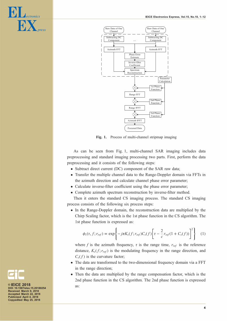
As can be seen from Fig. 1, multi-channel SAR imaging includes data
preprocessing and standard imaging processing two parts. First, perform the data
preprocessing and it consists of the following steps:
• Subtract direct current (DC) component of the SAR raw data;
• Transfer the multiple channel data to the Range-Doppler domain via FFTs in
the azimuth direction and calculate channel phase error parameter;
• Calculate inverse-filter coefficient using the phase error parameter;
• Complete azimuth spectrum reconstruction by inverse-filter method.
Then it enters the standard CS imaging process. The standard CS imaging
process consists of the following six process steps:
• In the Range-Doppler domain, the reconstruction data are multiplied by the
Chirp Scaling factor, which is the 1st phase function in the CS algorithm. The
1st phase function is expressed as:
�1ð�; f; rref Þ ¼ exp �j�Ksðf; rref ÞCsðfÞ � � 2
crref ð1 þ CsðfÞÞ
� �2( )ð1Þ
where f is the azimuth frequency, τ is the range time, rref is the reference
distance, Ksðf; rref Þ is the modulating frequency in the range direction, and
CsðfÞ is the curvature factor;
• The data are transformed to the two-dimensional frequency domain via a FFT
in the range direction;
• Then the data are multiplied by the range compensation factor, which is the
2nd phase function in the CS algorithm. The 2nd phase function is expressed
as:
Fig. 1. Process of multi-channel stripmap imaging
© IEICE 2018DOI: 10.1587/elex.15.20180254Received March 9, 2018Accepted March 22, 2018Publicized April 4, 2018Copyedited May 25, 2018
4
IEICE Electronics Express, Vol.15, No.10, 1–12
�2ðf�; f; rref Þ ¼ exp �j� f2�
Ksðf; rref Þ½1 þ CsðfÞ�� �
� exp j4�
cf�rrefCsðfÞ
� �ð2Þ
where f� is the range frequency. The first term of the expression completed the
range compression, including the secondary range compression (SRC), and the
second completed the range cell migration correction (SCRC);
• The data are transformed to Range-Doppler domain via an inverse FFT in the
range direction;
• Then the data are multiplied by the azimuth compensation factor to complete
the azimuth processing and phase correction. The azimuth compensation factor
is the 3rd phase function in the CS algorithm. The 3rd phase function is
expressed as:
�3ð�; f; rref Þ ¼ exp �j 2��c� 1 � 1 � �f
2Vðr ¼ �c=2Þ� �2
" #1=28<:
9=; þ j��ðf; rÞ
8<:
9=;ð3Þ
where ��ðf; rÞ ¼ 4�c2 Ksðf; rref Þ½1 þ CsðfÞ�CsðfÞðr � rref Þ2;
• An inverse FFT in the azimuth direction is executed, and focussed data are
obtained.
3 Implementation of SAR imaging system
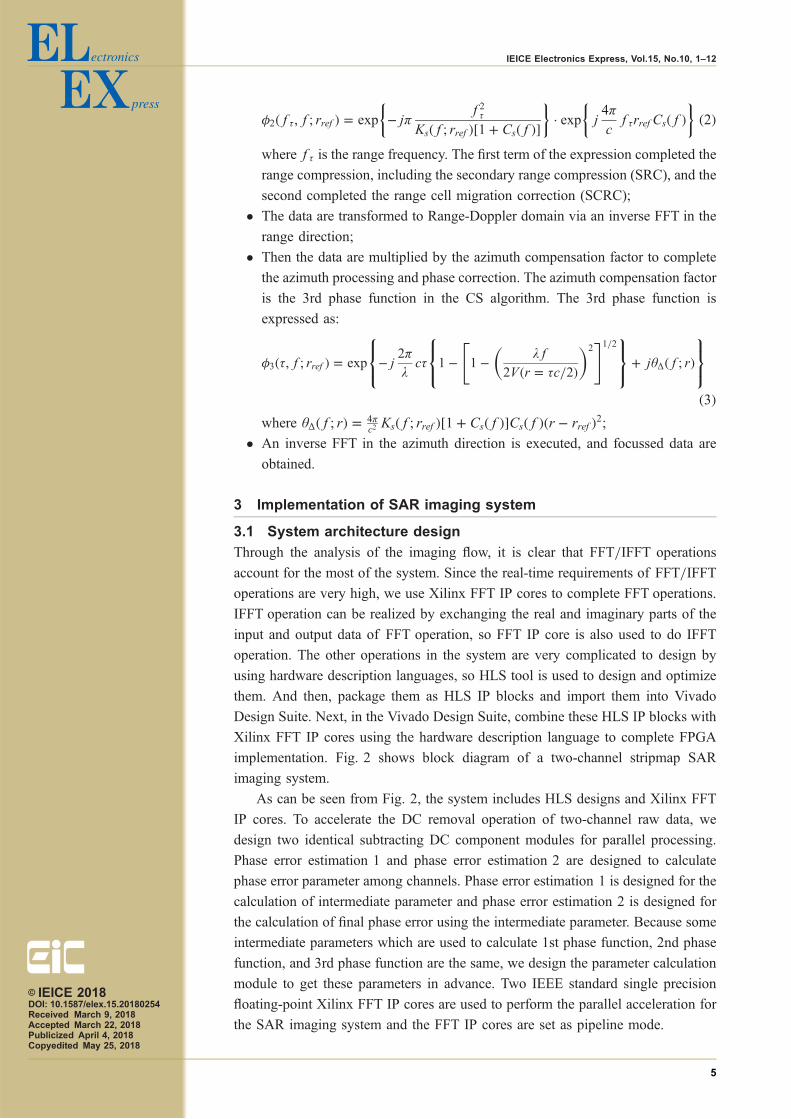
3.1 System architecture design
Through the analysis of the imaging flow, it is clear that FFT/IFFT operations
account for the most of the system. Since the real-time requirements of FFT/IFFT
operations are very high, we use Xilinx FFT IP cores to complete FFT operations.
IFFT operation can be realized by exchanging the real and imaginary parts of the
input and output data of FFT operation, so FFT IP core is also used to do IFFT
operation. The other operations in the system are very complicated to design by
using hardware description languages, so HLS tool is used to design and optimize
them. And then, package them as HLS IP blocks and import them into Vivado
Design Suite. Next, in the Vivado Design Suite, combine these HLS IP blocks with
Xilinx FFT IP cores using the hardware description language to complete FPGA
implementation. Fig. 2 shows block diagram of a two-channel stripmap SAR
imaging system.
As can be seen from Fig. 2, the system includes HLS designs and Xilinx FFT
IP cores. To accelerate the DC removal operation of two-channel raw data, we
design two identical subtracting DC component modules for parallel processing.
Phase error estimation 1 and phase error estimation 2 are designed to calculate
phase error parameter among channels. Phase error estimation 1 is designed for the
calculation of intermediate parameter and phase error estimation 2 is designed for
the calculation of final phase error using the intermediate parameter. Because some
intermediate parameters which are used to calculate 1st phase function, 2nd phase
function, and 3rd phase function are the same, we design the parameter calculation
module to get these parameters in advance. Two IEEE standard single precision
floating-point Xilinx FFT IP cores are used to perform the parallel acceleration for
the SAR imaging system and the FFT IP cores are set as pipeline mode.
© IEICE 2018DOI: 10.1587/elex.15.20180254Received March 9, 2018Accepted March 22, 2018Publicized April 4, 2018Copyedited May 25, 2018
5
IEICE Electronics Express, Vol.15, No.10, 1–12

3.2 Design and optimization of models on HLS
The design process of HLS can be divided into three main steps. Firstly, perform C
simulation to verify the function of modules. And the C/C++ testbench is designed
to ensure the correctness of the modules. In the case of ensuring the correctness of
the modules function, C synthesis can be performed directly which can convert
C/C++ model into RTL description. Finally, verify the RTL code with C/RTL co-
simulation by using the optimized C/C++ code and the original test stimulus.
Another step is exporting RTL as IP Catalog for system integration. HLS design
flow is roughly shown as Fig. 3.
Because HLS supports the operation of C/C++/SystemC language, we pro-
pose C++ language to directly program the modules that designed on HLS, and
optimize each module by modifying the directives until it meets the demand, and
converts all the modules into RTL description. Finally package the RTLs output as
IP blocks for SAR imaging system implementation.
Fig. 3. Design flow of HLS
Fig. 2. Block diagram of SAR imaging system
© IEICE 2018DOI: 10.1587/elex.15.20180254Received March 9, 2018Accepted March 22, 2018Publicized April 4, 2018Copyedited May 25, 2018
6
IEICE Electronics Express, Vol.15, No.10, 1–12

Vivado HLS has different directives for optimizing the integrated process of the
code to achieve different architectures, so the design has different running delays
and resource consumption. According to different requirements, we can quickly
reconfigure the function modules by modifying the related optimization directives
or parameters, and regenerate the RTL code which is with great flexibility. Since the
SAR imaging system requires high real-time, the PIPELINE, LOOP_MERGE, and
ARRAY_PARTITION directives are mainly used to optimize the data throughput
rate, reduce the delay and improve the performance of the modules. The target
device XC7VX690T is selected in the design of modules and the clock period is
10 ns.
In the following, the main optimization directives used in the modules are
described and the performance of some modules before and after the optimization
is shown. It should be explained that the optimization results of each module are
mostly the effect of multiple optimization directives.
(a) PIPELINE directive
Pipeline design is an important factor affecting the performance of a design. In
C/C++ based design of HLS, multiple executions of a task are performed
sequentially without the PIPELINE directive. Instruct a task to execute in a
pipeline, allowing the next execution of the task to begin before the current
execution is completed. It reduces the initiation interval by allowing the concurrent
execution of operations within a loop or function. This directive is used in loops or
functions in the modules designed on HLS and is optimized by setting the
processing latency of the pipeline sub-steps. Take phase function generation
calculation module as an example to illustrate the effect of PIPELINE directive.
Table I and Table II respectively show the performance and resource utilization of
1st phase function, 2nd phase function and 3rd phase function generation calcu-
lation modules before and after optimization.
Table I. Performance comparison of phase function calculationmodules before and after optimization
ModulesLatency Interval
Before After Before After
1st phase function 86017 4117 86018 41182nd phase function 507939 16449 507940 16450
3rd phase function 758083 8534 758084 8535
Table II. Resource utilization comparison of phase function calcula-tion modules before and after optimization
Modules Optimization BRAM_18K DSP48E FF LUT
1st phase Before 0 16 1231 1204function After 0 35 2295 17692nd phase Before 0 41 6693 10182function After 0 58 8339 121243rd phase Before 16 44 11253 16442function After 16 207 29140 42853© IEICE 2018
DOI: 10.1587/elex.15.20180254Received March 9, 2018Accepted March 22, 2018Publicized April 4, 2018Copyedited May 25, 2018
7
IEICE Electronics Express, Vol.15, No.10, 1–12

(b) LOOP_MERGE directive
By default, HLS performs multiple consecutive loops sequentially. With LOOP_
MERGE directive, multiple loops can be implemented in parallel which can reduce
overall latency, increase sharing and improve logic optimization. The directive
can’t be used if there is data dependency among loops. Besides, loops cannot be
merged when they contain FIFO reads. Merging changes the order of the reads,
however reads from a FIFO or FIFO interface must always be in sequence. Take
phase error estimation 1 module as an example to illustrate the effect of LOOP_
MERGE directive. Its performance and resource utilization before and after
optimization of LOOP_MERGE directive are shown in Table III and Table IV.
(c) ARRAY_PARTITION directive
In the optimization of algorithms, PIPELINE directive which is commonly used
to improve performance is often limited because of the inability to satisfy multiple
accesses to an array at the same time, and the optimization effect is affected.
ARRAY_PARTITION directive can partition large arrays into multiple smaller
arrays or into individual registers, improving access to data and remove block RAM
bottlenecks. HLS provides three types of array partitioning: block, cyclic and
complete. According to different rules and needs of algorithms, select an appro-
priate array partitioning type. ARRAY_PARTITION directive is usually applied
with other directives, and it helps in reducing latency.
Subtracting DC data module, parameter calculation module, phase error esti-
mation 2 module and inverse-filter coefficient calculation module use one or two or
three directives shown above. Specific optimization is no longer shown one by one
and Table V shows the usage of directives on modules.
Table III. Performance comparison of phase error estimation 1module before and after optimization
ModulesLatency Interval
Before After Before After
Phase error estimation 1 16415 8211 16416 8212
Table IV. Resource utilization comparison of phase error estimation 1module before and after optimization
BRAM_18K DSP48E FF LUT
Before 0 20 4551 5378After 0 23 4505 5279
Table V. Usage of optimization directives of modules
Modules PIPELINE LOOP_MERGE ARRAY_PARTITION
Subtracting DC data ✓
1st phase function ✓
2nd phase function ✓
3rd phase function ✓
Parameter calculation ✓ ✓ ✓
Phase error estimation 1 ✓ ✓ ✓
Phase error estimation 2 ✓
Inverse-filter coefficient ✓ ✓
© IEICE 2018DOI: 10.1587/elex.15.20180254Received March 9, 2018Accepted March 22, 2018Publicized April 4, 2018Copyedited May 25, 2018
8
IEICE Electronics Express, Vol.15, No.10, 1–12

As can be seen from the performance and resource utilization of each module
before and after the optimization, the latency and throughput of each module has
greatly improved, and resource utilization has increased a little. Considering the
high real-time requirements of real-time imaging system, it is paramount to meet
the performance requirements in the optimization process and the increment in
resource utilization is allowed as long as it is within acceptable limits. Therefore,
the modules designed with HLS meets the requirements.
3.3 Real-time performance analysis
The architecture of the imaging system mentioned in section 3.1 is based on a
combination of HLS-design IP blocks and FFT IP cores. If the entire system is
divided on a time scale, it can be divided into three large modules. As shown in
Fig. 4, the three modules are azimuth spectrum reconstruction, range data process-
ing and azimuth data processing, which belong to a serial operation in time. That is,
all data of the current module is processed before the data processing of the next
module can be performed.
The real-time performance analysis of a two-channel SAR imaging system by
processing SAR raw data with a granularity of 16384 � 4096 is shown below. As
we know, the data available to a SAR processor are an ensemble of two-dimen-
sional dispersed signals. We assume that NAA represents sampling points in azimuth
direction of raw data, NA represents sampling points in azimuth direction of data
after spectrum reconstruction, and NR represents sampling points in range direc-
tion. Based on the assumption, NAA is equal to 2048, NA is equal to 4096 and NR is
equal to 16384. The device model used in this paper is Xilinx XC7VX690T,
instantiating two FFT IP cores in the device for parallel processing.
(a) Analysis of stage �1Firstly, subtract the DC component from SAR raw data, and we design and package
Fig. 4. Real-time imaging system analysis process
© IEICE 2018DOI: 10.1587/elex.15.20180254Received March 9, 2018Accepted March 22, 2018Publicized April 4, 2018Copyedited May 25, 2018
9
IEICE Electronics Express, Vol.15, No.10, 1–12

two IP blocks to ensure that two-channel data can be processed in parallel, which
consumes nearly 1.5 s. Then the processing of the data is partitioned into two
parallel branches. One branch, calculate phase error parameter between the two
channels using all the data. The other branch, execute NR times azimuth NAA-point
FFT individually with two FFT IP cores. The speed of the FFT operation is faster,
so the delay of this part depends on the calculation of phase error parameter. When
the two-channel phase error parameters are obtained, the calculation of inverse-
filter coefficients are begun to be executed. This section is executed sequentially,
with a total delay of approximately 1.5 s. After that, the filtering operation is
performed. Two pieces of NAA-point data execute filtering operation at the same
time to get a piece of NA-point data, and then the data are multiplied by the 1st
phase function. The filtering operation can be parallelized with the calculation of
the 1st phase function. Since the speed of the calculation of 1st phase function is
slower, the delay depends on the 1st phase function part. The partial delay is about
0.5 s, and the azimuth processing completes.
(b) Analysis of stage �2After the azimuth data processing is finished, the range operation is performed. This
section is a part of the flow of the classical CS imaging algorithm. The FFT
operation in the range direction is executed and then the data are multiplied by the
2nd phase function, and finally the inverse FFT is executed in the range direction.
This part we uses two FFT IP cores with the pipeline structure. In this case, for NR-
point FFT processing, it takes approximately NR clock cycles to receive data, NR
clock cycles to process data and NR clock cycles to release Data. And multiple
pieces of data can be pipelined with the pipeline structure. Considering that the
computational delay of one piece of 2nd phase function is about 16449 clock
cycles, it is obviously not enough to update one piece of 2nd phase function per
piece of data. In order to make the computational speed of 2nd phase function
match with FFT operation, we propose a method that every four pieces of data share
one piece of the 2nd phase function and adopt the ping/pong memory group as
caches for the 2nd phase function. Since two FFT IP cores are used to process two
pieces of data in parallel, it means that we update one piece of the 2nd phase
function every two pieces of data for one FFT IP core. This method has been
verified to have little effect on imaging quality, and the 2nd phase function
computational speed can match with the FFT operation. In this case, the total
delay depends on the FFT operation, and the total processing time of NA pieces of
data takes about 0.35 s. After that, the inverse FFT operation in the range direction
is executed with the latency of about 0.35 s.
(c) Analysis of stage �3The data are multiplied by the 3rd phase function, and then the inverse FFT in the
azimuth direction is executed. The time schedule of this part is similar to the range
operation. The difference is that the inverse FFT operation in the azimuth direction
can be executed only after the data have been multiplied by the 3rd phase function.
In order to match the speed of the calculation of the 3rd phase function to the
inverse FFT operation, we propose a method that every six pieces of data share one
piece of the 3rd phase function, which means that one piece of the 3rd phase
function is updated for every three pieces of data for one FFT IP core, and it has no
© IEICE 2018DOI: 10.1587/elex.15.20180254Received March 9, 2018Accepted March 22, 2018Publicized April 4, 2018Copyedited May 25, 2018
10
IEICE Electronics Express, Vol.15, No.10, 1–12

effect on imaging quality. The partial delay is the sum of the latency of the first
piece of the 3rd phase function calculation and the inverse FFT operation, which is
about 0.35 s.
4 Results
The two-channel stripmap SAR imaging system is validated by processing SAR
raw data with a granularity of 16384 � 4096. The raw data are represented in a
single precision floating point complex form with 64 bit (32 bit for the real part
and for the imaginary part, respectively) for each sample data point. The Xilinx
XC7VX690T FPGA is used as the platform of the imaging node, and two FFT IP
cores are adopted for parallel processing. The imaging system is evaluated from
three aspects: image quality, performance and resource utilization. Fig. 5 is a point
target image, which is imaged by the two-channel stripmap SAR imaging system.
And the horizontal direction is the range direction and the vertical direction is the
azimuth direction.
Peak side-lobe ratio (PSLR), integrated side-lobe ratio (ISLR) and spatial
resolution (RES) are used to evaluate the point target. R represents the range
direction and A represents the azimuth direction. During the imaging process, a
two-dimensional windowing process was performed with a −30 dB Taylor window.
As can be seen from Table VI, the comparison between the two cases does not
differ widely, which validates that the proposed imaging system is able to provide
sufficient accuracy for point target imaging.
Through recording the numbers of clock cycles, it takes 4.7 s for the system
to process SAR raw data with 16384 � 4096 data granularity at the operating
frequency of 100MHz. Table VII shows the resource utilization of 16384 � 4096
sample points processed by the proposed imaging system.
Table VIII shows a comparison with previous works. Compared with [13, 14],
taking into account the data granularity processed, the proposed system shows
advantages in processing time. Reference [12] describes a stripmap SAR system
Fig. 5. Point target image
Table VI. Comparison of FPGA imaging and Matlab imaging
PlatformR
PSLR(dB)
RISLR(dB)
RRES(m)
APSLR(dB)
AISLR(dB)
ARES(m)
FPGA −29.69 −24.86 1.52 −28.95 −24.37 1.05Matlab −29.72 −24.89 1.50 −29.02 −24.46 1.03
© IEICE 2018DOI: 10.1587/elex.15.20180254Received March 9, 2018Accepted March 22, 2018Publicized April 4, 2018Copyedited May 25, 2018
11
IEICE Electronics Express, Vol.15, No.10, 1–12

and it takes 12.1 s to process stripmap SAR raw data with a granularity of 16384 �16384. Since the system we designed is a two-channel stripmap SAR imaging
system, the inverse-filter method is executed to complete data preprocessing which
consumes more time than that of stripmap SAR imaging system. Taking into
account the data granularity and the complexity of the algorithm, the processing
time of reference [12] is comparable to ours. And the resource utilization of our
design is acceptable.
In summary, the proposed design achieves a good tradeoff between real-time
performance and resource utilization. The entire design takes 12 weeks from initial
software code simulation to the final imaging, and it demonstrates that HLS can
improve the design productivity.
5 Conclusion
Vivado HLS tool is applied to design and implement a multi-channel stripmap SAR
imaging system on an FPGA platform. And a two-channel imaging system is
implemented on Xilinx XC7VX690T FPGA platform by combining HLS designs
and FFT IP cores. The modules designed on HLS are optimized and packaged as
IP blocks for FPGA implementation. The proposed system takes 4.7 s to process
SAR raw data with 16384 � 4096 data granularity. And the image quality and
resource utilization of the system is acceptable. Designing on the basis of existing
reliable software codes on HLS reduces the difficulty of FPGA development and
accelerates the implementation of a multi-channel stripmap SAR imaging system.
The evaluation of the SAR imaging system illustrates the effectiveness of HLS as a
flexible design tool for FPGA implementation.
Acknowledgments
This work was supported by the National Natural Science Foundation of China
under Grant 91438203, the Chang Jiang Scholars Program under Grant T2012122
and the Hundred Leading Talent Project of Beijing Science and Technology under
Grant Z141101001514005.
Table VII. Resource utilization of SAR imaging system (XilinxXC7VX690T)
Resource Utilization Available Utilization (%)
LUT 227577 433200 52.53LUTRAM 7931 174200 4.55
FF 157038 866400 18.13BRAM 295 1470 20.07DSP 838 3600 23.28
Table VIII. Comparison with previous works
Works Years SchemesData
granularityWorkingfrequency
Processingtime
Proposed 2018 FPGA 16384 � 4096 100MHZ 4.7 s[12] 2017 FPGA+ASIC 16384 � 16384 100MHZ 12.1 s[13] 2016 GPU 2048 � 2048 - 3.2 s[14] 2008 Multi-DSP 4096 � 4096 100MHZ 13 s
© IEICE 2018DOI: 10.1587/elex.15.20180254Received March 9, 2018Accepted March 22, 2018Publicized April 4, 2018Copyedited May 25, 2018
12
IEICE Electronics Express, Vol.15, No.10, 1–12