Embed Size (px)
Citation preview
1
School of Engineering and Physical Sciences
Department of Electrical Electronic and Computing Engineering
Master of Science Dissertation
Design and Fabrication of Multilayer Piezoelectric NEMS Resonators
Muhammad Faizan
July 2016
Supervisors: Prof. Guillermo Villanueva (EPFL)
Prof. Marc Desmulliez (HWU)

2
Abstract
We have successfully demonstrated the fabrication of self-actuating multilayer NEMS resonators
including cantilevers and double clamped beams. Resonant sensors are widely used as precision
mass sensors for the detection and quantification of small concentration of analyte molecules in
a gaseous solution or bacteria from biological sample which requires extremely high mass
sensitivity and responsivity of the resonant sensor. Nanofabrication techniques have enabled the
use of ultrathin layers for the fabrication of resonant sensors to significantly enhance sensitivity
by reducing the mass of the sensor. Aluminum nitride (AIN) as an ultra-thin PZE layer has
significant advantages over other transduction techniques due to its high PZE efficiency, good
mechanical and thermal stability and compatibility with CMOS processing. 50nm ultra-thin layer
of AIN was deposited over 25nm thin layer of platinum (Pt) in order to get well textured columnar
growth of AIN crystals. AIN deposition parameters were carefully optimized to enhance
piezoelectric response. The residual stress and piezoelectric properties of AIN film were studied
as a function of deposition conditions. Short circuiting of electrodes was the most critical problem
which was solved after implementing two different process flows. Oxide bridges were fabricated
in order to avoid unwanted electrical contact between different metallic layers. At the end,
suspended cantilevers and beams were suffering from bending due to high compressive stress in
the active layer. Residual stress of -169.80 MPa was calculated using Stoney formula by
measuring the curvature of wafer before and after the deposition of individual layers.
Numerous studies have already been done on shifting of the resonance frequency due to the
variations in attached mass on the surface of a resonator but there is still room for the
investigation of surface stress changes on the resonance frequency. Application of surface stress
induces a change in beam stiffness and dimensions which alter the resonance frequency of the
cantilevers and doubly clamped beams. The motivation of this project was to carried out different
experiments to study the effect of surface stress on the resonance frequency by using an active
piezoelectric layer for the actuation of resonant structures. Application of voltage across PZE
layer generates a longitudinal stress across the beam which leads to a shift in resonance
frequency. Vibrometer was used to find the resonance frequency of the released devices.

3
Acknowledgements
I would like to thank my project supervisors Prof. Guillermo Villanueva from EPFL and Prof. Marc
Desmulliez from HWU for their support and guidance throughout the project. Their valuable
advice and technical discussions helped me in increasing my knowledge of the respective field
and achieving the project objectives successfully.
Secondly, I would like to express my sincerest gratitude to Annalisa De Pastina for helping me out
in the fabrication of oxide bridges. Special thanks to Kaitlin Howell, Andrea Lozzi, Marco and all
the members of Advance NEMS group for making my stay cheerful and wonderful.
Last but not the least, I am grateful to my parents for their encouragement and unwavering
support throughout the duration of my master dissertation.

4
Table of Contents Chapter 1: Introduction ......................................................................................................................8
1.1. Background .......................................................................................................................................... 8
1.2. MEMS/NEMS Resonator ................................................................................................................... 10
1.3. Microcantilever Beam Resonator ...................................................................................................... 10
1.3.1. Modes of Operation ............................................................................................................... 11
1.3.2. Commonly used methods of resonator excitation and detection principles......................... 12
1.3.3. Applications of Micro cantilever Resonators ......................................................................... 15
Chapter 2: Multilayer Piezoelectric NEMS Resonator ........................................................................ 19
2.1. Piezoelectricity .................................................................................................................................. 19
2.1.1. Piezoelectric Coefficients ....................................................................................................... 19
2.1.2. Piezoelectric Charge Coefficients ........................................................................................... 20
2.2. Proposed design of Multilayer Piezoelectric Resonator ................................................................... 20
2.3. Aluminum nitride material characterization ..................................................................................... 21
2.3.1. DC Pulsed reactive magnetron sputtering for AIN thin films ................................................. 22
2.3.2. Effect of deposition conditions on AIN growth ...................................................................... 23
2.3.3. Platinum electrode layer for AIN thin film growth ................................................................. 28
2.4. Optimization of AIN deposition parameters ..................................................................................... 30
Chapter 3: Finite element analysis of multilayer piezoelectric resonators .......................................... 33
3.1. Structural Analysis ............................................................................................................................. 34
3.2. Modal Analysis .................................................................................................................................. 36
Chapter 4: Fabrication ...................................................................................................................... 39
4.1. First Process Flow .............................................................................................................................. 40
4.1.1. Mask Design ........................................................................................................................... 41
4.1.2. Experimental Work ................................................................................................................. 42
4.1.3. Discussion ............................................................................................................................... 53
4.2. Second process flow .......................................................................................................................... 58
4.2.1. Mask Design ........................................................................................................................... 59
4.2.2. Experimental work ................................................................................................................. 60
4.2.3. Discussion ............................................................................................................................... 71
4.3. Resonance frequency measurements ............................................................................................... 74
5. Conclusion ................................................................................................................................. 76
6. References ................................................................................................................................ 78

5
List of Figures
Figure 1: Components of MEMS smart system ............................................................................................ 8
Figure 2: Application areas of MEMS resonators ....................................................................................... 10
Figure 3: Cantilever sensor modes of operation: (A) dynamic mode detecting mass changes on the
cantilever by changes in resonance frequency; (B) bimetallic mode detecting temperature changes by a
static bending due to different thermal expansion of the metal layer and silicon cantilever; (C) static
mode where asymmetrical molecule absorption cause tensile stress, results in bending the cantilever
upwards; (D) static mode where asymmetrical molecule absorption cause compressive stress, results in
bending the cantilever downwards [15] ..................................................................................................... 11
Figure 4: Block diagram of a resonant sensor ............................................................................................. 12
Figure 5: Different excitation and detection techniques for microcantilever resonators [18] .................. 14
Figure 6: Basic components of a chemical sensor ...................................................................................... 16
Figure 7: SEM image of silicon-based resonant cantilever with hexafluoro-2-propanol functionalized
mesoporous silica sensing film [31] ............................................................................................................ 16
Figure 8: PZT based self-sensing microcantilever [36] ................................................................................ 17
Figure 9: Direction of forces affecting a piezoelectric element .................................................................. 19
Figure 10: Block diagram of Multilayer Piezoelectric Resonator ............................................................... 21
Figure 11: Schematic diagram illustrating the basic components of a magnetron sputtering system [49]
.................................................................................................................................................................... 22
Figure 12: Basic mechanism of Pulsed DC magnetron sputtering. Positive pulse reverse the potential on
the target and attracts electrons in order to neutralize the positive charge buildup on the insulator
surface [52] ................................................................................................................................................. 23
Figure 13: Rate of deposition of AIN film as function of substrate temperature [53] ............................... 24
Figure 14: SEM cross-sectional view of AlN thin films deposited at different substrate temperatures of (a)
60 0C (b) 160 0C (c) 250 0C (d) 340 0C (e) 430 0C (f) 520 0C [53] ................................................................... 25
Figure 15: AIN film deposition rate for different nitrogen flow rates [55] ................................................. 26
Figure 16: Residual stress in AIN grown on Pt, Al and Ti as a function of gas flow rates [56] .................... 26
Figure 17: Piezoelectric coefficient d33 of AIN grown on Pt, Al and Ti as a function of gas flow rates [56]
.................................................................................................................................................................... 27
Figure 18: Piezoelectric coefficient d33 of AIN grown on Pt, Al and Ti as a function of sputtering pressure
[56] .............................................................................................................................................................. 27
Figure 19: Residual stress of AIN grown on Pt, Al and Ti as a function of sputtering pressure [56] .......... 28
Figure 20: Measured residual stress (solid diamond) and stress derived from out-of-plane strain (XRD-
open circles) as a function of AlN thin-film thickness [60] ......................................................................... 29
Figure 21: Cross section of an AlN film. The left side shows the film grown on (111)-oriented Pt and the
right side shows the growth on thermal SiO2 [61] ...................................................................................... 29
Figure 22: Fabricated test structures for resistance measurements .......................................................... 31
Figure 23: Top and bottom platinum contact pads for resistance measurements .................................... 32
Figure 24: Structural geometry of proposed cantilever design .................................................................. 33
Figure 25: Deflection of the cantilever beam under the influence of 2V ................................................... 34

6
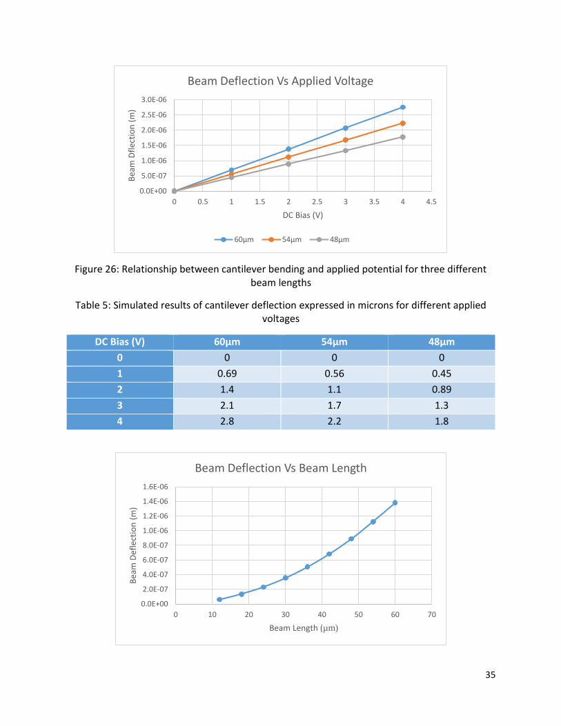
Figure 26: Relationship between cantilever bending and applied potential for three different beam
lengths ......................................................................................................................................................... 35
Figure 27: Deflection of cantilever for different beam lengths .................................................................. 36
Figure 28: Reduction in first modal resonance frequency of the cantilever with increase in beam length
.................................................................................................................................................................... 37
Figure 29: First three mode shapes of a 60x6µm cantilever under no loading force; (a) fres of first mode is
39879 Hz; (b) fres of second mode is 2.4981e+5 Hz; (c) fres of third mode is 7.0002e+5Hz ........................ 38
Figure 30: (a) First mask layer for patterning of bottom platinum layer; (b) Second mask layer for
patterning of top platinum layer ................................................................................................................ 41
Figure 31: (a) Third mask layer for patterning of devices on top platinum layer; (b) Fourth mask layer for
patterning of contact pads .......................................................................................................................... 42
Figure 32: Alignment marks ........................................................................................................................ 42
Figure 33: Appearance of silver color after Pt layer deposition ................................................................. 43
Figure 34: First mask layer to pattern bottom Platinum layer electrode ................................................... 44
Figure 35: Appearance of purple color gives an indication of complete etching of top layers and shows
that underneath AIN layer has been exposed ............................................................................................ 45
Figure 36: Second mask layer to pattern top Platinum layer electrode ..................................................... 47
Figure 37: Fitting of plus (+) sign inside the square shows the perfect alignment of second layer with the
first layer ..................................................................................................................................................... 47
Figure 38: Third mask layer to pattern devices .......................................................................................... 49
Figure 39: Photolithography results after development of device layer .................................................... 49
Figure 40: Photolithography results of 5µm wide cantilevers after development..................................... 50
Figure 41: Poor photolithography results for 1µm wide cantilevers due to overexposure ....................... 50
Figure 42: Making of openings for structure releasing ............................................................................... 51
Figure 43: Released cantilever after wet etching of oxide layer ................................................................ 52
Figure 44: Cantilever suffering from stiction .............................................................................................. 52
Figure 45: Processes involved in dry etching and formation of fences due to redeposition of etched
material on the side walls ........................................................................................................................... 53
Figure 46: Formation of high fence on the edge of platinum layer after dry etching ................................ 53
Figure 47: SEM image shows the possible region of failure where top Pt layer step onto the bottom Pt
layer ............................................................................................................................................................ 54
Figure 48: SEM image showing fences of bottom Pt layer that are visible on the top Pt layer ................. 55
Figure 49: SEM image showing unwanted material connecting top and bottom platinum layers ............ 55
Figure 50: Formation of fences after etching platinum layer in STS ........................................................... 56
Figure 51: Underneath Pt layer has been exposed after unwanted etching of mask layer ....................... 57
Figure 52: (a) First mask layer for patterning of top platinum layer; (b) Second mask layer for patterning
of bottom platinum layer ............................................................................................................................ 59
Figure 53: (a) Third mask layer for patterning of SiO2 bridges; (b) Fourth mask layer for patterning of
contact pads ................................................................................................................................................ 60
Figure 54: Fifth mask layer for patterning of devices on top platinum layer ............................................. 60
Figure 55: First mask design layer to pattern top Pt layer .......................................................................... 61
Figure 56: Second mask layer for patterning of bottom Pt layer ............................................................... 62
Figure 57: Third mask layer for patterning of SiO2 bridges ......................................................................... 62
Figure 58: Fabrication of SiO2 bridges for electrical insulation between different layers .......................... 63

7
Figure 59: Broken SiO2 bridges due to over etching of SiO2 layer in BHF ................................................... 63
Figure 60: Illustration of the liftoff process ................................................................................................ 64
Figure 61: Fourth mask layer for patterning of gold contact pads ............................................................. 65
Figure 62: Photolithography of contact pads for gold deposition .............................................................. 65
Figure 63: After 100nm of gold deposition ................................................................................................. 66
Figure 64: Fabrication of gold pads and lines for the electrical connection with the top Pt layer ............. 66
Figure 65: Gold line passing over the oxide bridge ..................................................................................... 67
Figure 66: Fourth mask layer for the patterning of devices ....................................................................... 67
Figure 67: Anisotropic etching of silicon using Bosch process .................................................................... 68
Figure 68: Cantilever tips are out of focus due to bending downwards .................................................... 69
Figure 69: SEM image showing etched cavity and released cantilevers and doubly clamped beams ....... 69
Figure 70: SEM image of released devices .................................................................................................. 70
Figure 71: Over etching of silicon from underneath the anchored platform ............................................. 70
Figure 72: Working principle of Toho Technology FLX 2320-S ................................................................... 71
Figure 73: Simulation of cantilever with material stress in ANSYS Multiphysics ........................................ 72
Figure 74: Fabricated multilayer piezoelectric resonators ......................................................................... 73
Figure 75: PCB mounted and wirebonded with the chip for providing voltage signal to the resonators .. 74
Figure 76: Resonance frequency of 60µm long cantilever measured with Laser Vibrometer MSV-400 ... 75
Figure 77: Appearance of cracks on the top platinum layer when voltage was exceeded the threshold
limit. SEM image on the right shows the rupturing of layers ..................................................................... 76
List of Tables Table 1: Commercial MEMS based applications [1] ..................................................................................... 9
Table 2: Piezoelectric Charge Coefficients .................................................................................................. 20
Table 3: Test wafers deposited with different deposition conditions for AIN film growth ........................ 30
Table 4: Material properties for FEM ......................................................................................................... 34
Table 5: Simulated results of cantilever deflection for different applied voltages .................................... 35
Table 6: Data set for cantilever deflection for different beam lengths ...................................................... 36
Table 7: Data set for the first modal resonance and prestressed resonance frequencies for different
beam lengths............................................................................................................................................... 37
Table 8: Optimized deposition rates for SPIDER ......................................................................................... 43
Table 9: SPIDER Deposition parameters for AIN, Pt and SiO2 films ............................................................ 43
Table 10: Approx. etch rates of SiO2 and Pt for Nexus IBE350 ................................................................... 45
Table 11: Optimized deposition rates for SPIDER ....................................................................................... 46
Table 12: Etch rates and etch time of SiO2, Pt and AIN for STS Multiplex .................................................. 48
Table 13: Etch rates and etch time of SiO2, Pt and AIN for STS Multiplex .................................................. 51
Table 14: Deposition rates and time of different layers for SPIDER ........................................................... 61
Table 15: Parameters for coating of LOR and AZ 1512 in ACS200 .............................................................. 64
Table 16: Calculated stress values for individual layers and the overall stress measured by Toho
Technology FLX 2320-S ............................................................................................................................... 72

8
Chapter 1: Introduction
1.1. Background MEMS has become a hallmark technology for the 21st century. The advancement in MEMS
technology has opened new doors for many emerging applications in the field of smart sensors
and actuators. MEMS stands for Micro Electro Mechanical Systems. As the name implies, it refers
to the integration of miniaturized electrical and mechanical elements into micro scale system.
The critical dimensions of MEMS devices can vary from well below one micron to few millimeters
[1]. MEMS technology has potential to revolutionize industrial and consumer products by
incorporating Integrated Circuits (IC) batch processing techniques with micromachining
processes. It offers the possibility of integration of mechanical, electromechanical,
electrochemical and optical components along with the signal processing control circuitry on a
single chip to produce smart sensing devices [2]. The basic components of MEMS smart system
consist of mechanical microstructures, microsensors, microactuators and microelectronics as
shown in Figure 1. Microsensors and microactuators are categorized as transducers that convert
energy from one form to another. Microsensors are used to detect any change such as pressure,
thermal, chemical or electromagnetic, in the physical environment of the system and convert it
into a readable electrical signal. The electrical signal can be a change in voltage, current or
resistance, etc. Microelectronics makes a decision on the basis of information provided by the
sensing element and signal the microactuators to react and perform mechanical motion in order
to bring some specific changes in the physical environment of the system [3].
Figure 1: Components of MEMS smart system
The research on MEMS started in early 1960s but it took 20 to 30 years for the first MEMS device
to be commercially available. Micromachined nozzles for inkjet printers and accelerometers for
Microsensors Microactuators
MEMS
Microelectronics Microstructures
9
airbag system were first few commercial applications of MEMS devices. In 1980s, the
advancement in MEMS technology has seen a very rapid growth due to the introduction of new
microfabrication processes derived from well-established semiconductor Integrated Circuit (IC)
manufacturing. These processes include lithography, thin film deposition and different wet and
dry etching techniques. There are many mature MEMS devices available in the market, which are
incorporated into bigger systems to provide commodities for our daily life [4].
In the today’s world, the technological boom of the Internet of Things is entirely dependent on
accurate and reliable sensors for data gathering. In such an industry, the need for miniaturization
is essential and the demand for smart microsystems is ever growing. MEMS devices have huge
impact on microsystems industry due to their small size, high reliability and low cost [5]. MEMS
devices can be used in various technological fields including telecommunication, data storage,
medical, automotive and environmental monitoring. Table 1 shows some of the commercial
applications of MEMS devices.
Table 1: Commercial MEMS based applications [1]
In 1959, the physicist Richard Feynman gave a visionary talk in an American Physical Society
meeting at Caltech entitled as “There's Plenty of Room at the Bottom” [6]. This talk was about
the direct manipulation and arrangement of atoms by the help of nanoscale machines. At that
moment, it did not get enough attention but later his ideas laid the foundation of
nanotechnology. Nanotechnology is a field of science that deals with the inspection and
manipulation of individual atoms and molecules with the dimension of 1 to 100 nanometers [7].
The ideas floated by Richard Feynman decades ago, are now transformed into well-established
fields of technology such as electron and ion beam fabrication, molecular beam epitaxy,
nanoimprint lithography, atom-by-atom manipulation and micro/nanoelectromechanical
systems (M/NEMS) [8].
Applications Examples
Sensors Pressure sensor, bio-metric sensor, IR sensor, motion sensor
Resonators Inertial sensor, gyroscope, accelerometer
Actuators Motor, drive
Audio MEMS Microphone
Printer 3D printer, ink-jet printer using piezoelectric and thermal bubble ejection
Bio-MEMS Fluid acceleration for micro-cooling, lab on chip, µ-TAS (biosensor etc)
Micropump Electroactive polymer, active microfluidic handling or analysis
Optics Optical switches for data communication, MEMS micro-mirrors
Energy Harvest Micro power generators based on piezoelectric, electrostatics and electromagnetics
Display Projection display, reflective display, tactile display
10
NEMS is one step ahead of MEMS in terms of miniaturization, device efficiency and low cost. The
devices such as resonance mass sensors are greatly affected by the dimensions of the mechanical
sensing element. The sensitivity and the quality factor can be improved by scaling down the
dimensions and mass of the sensor [9][10].
1.2. MEMS/NEMS Resonator Resonator is a mechanical structure which vibrates at a particular frequency with relatively
greater amplitude. This particular frequency is called the resonance or natural frequency of the
system. MEMS resonators are miniaturized devices having resonating mechanical elements such
as cantilever, double clamped beam or a membrane that oscillates at resonance frequency upon
excitation. Excitation stimulus can be voltage, current or force. MEMS resonators have found
their way in consumer industry as a part of different sensing devices such as mass, pressure and
gas sensors. The readout parameter for a resonance sensor can be changed in resonance
frequency, quality factor, vibration amplitude and phase which are directly affected by the axial
forces, added mass, change in damping, material properties and magnitude of driving force.
Figure 2 summarizes different types of parameters that can be detected by a MEMS resonant
sensor and its corresponding output [11].
Figure 2: Application areas of MEMS resonators
1.3. Microcantilever Beam Resonator Microcantilever is a most common type of MEMS resonator. Cantilever is a mechanical beam
which is anchored at one end and free to move at the other end. Over the past few years,
microcantilevers have gain a lot of attention due to high sensitivity in different sensing
applications. Pressure sensor, chemical sensor and mass sensor are few examples where the
11
magnitude of beam deflection or change in resonant frequency of the beam is used to measure
the change in the physical environment of the device depending upon the mode of operation
[12].
1.3.1. Modes of Operation
Sensors based on microcantilevers can be operated in dynamic mode or static mode. In dynamic
mode of operation, the change in resonance frequency of the beam is measured. Microcantilever
based mass sensors can be operated in dynamic mode where the change in resonance frequency
gives the measure of mass absorbed on the surface of the cantilever as shown in Figure 3A. In
dynamic mode, the cantilever is excited close to its resonance frequency. When the additional
mass is attached to the surface of cantilever it shifts the resonance frequency. Frequency of the
cantilever reduces as the amount of absorbed mass increases. The change in resonance
frequency ∆fres due to absorbed mass ∆m is given by equation 1 [13][14].
∆𝑓𝑟𝑒𝑠 ≈ −𝑓0
∆m
2𝑚0
where f0 is the natural frequency and mo is the initial mass of the cantilever.
Figure 3: Cantilever sensor modes of operation: (A) dynamic mode detecting mass changes on
the cantilever by changes in resonance frequency; (B) bimetallic mode detecting temperature
changes by a static bending due to different thermal expansion of the metal layer and silicon
cantilever; (C) static mode where asymmetrical molecule absorption cause tensile stress, results
in bending the cantilever upwards; (D) static mode where asymmetrical molecule absorption
cause compressive stress, results in bending the cantilever downwards [15]
In static mode of operation, bending of the cantilever is continuously monitored for the detection
of any change in the external measurands. Deflection of the cantilever beam can be caused by
the variation in surface stress, pressure or temperature. Most of the bio-sensors operate in fluid
environment where the dynamic mode of operation cannot be used because quality factor is
drastically reduced due to the viscous damping of the fluid [16]. So sensing is done by using beam
deflection. One side of the cantilever is coated with monolayer of bio-receptors in order to attach
selective molecules from the fluid whereas the other side is kept inert. This creates an
(1)
12
asymmetrical stress on the surface which deflects the cantilever [17]. Depending on the type of
stress generated, the cantilever beam will bend upwards or downwards. In case of compressive
stress, the cantilever bends downwards whereas it bends upwards for tensile stress as shown in
Figure 3C and 3D. The magnitude of beam deflection gives the amount of change in surface stress
which gives an indication regarding the amount of molecules attached on the surface. Stoney’s
formula is one of the most commonly used equation that relates beam deflection with the change
in surface stress and the beam dimensions as shown in equation 2 [15].
∆𝜎 =𝐸𝑡2
3(1 − 𝑣)𝐿2∆𝑧
Where ∆𝜎 is the change in surface stress between top and bottom surface of the cantilever, ∆z
is the cantilever deflection, E is Young’s modulus, 𝑣 is Poisson ratio and L and t are the length and
the thickness of the beam respectively.
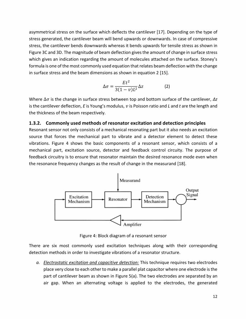
1.3.2. Commonly used methods of resonator excitation and detection principles Resonant sensor not only consists of a mechanical resonating part but it also needs an excitation
source that forces the mechanical part to vibrate and a detector element to detect these
vibrations. Figure 4 shows the basic components of a resonant sensor, which consists of a
mechanical part, excitation source, detector and feedback control circuity. The purpose of
feedback circuitry is to ensure that resonator maintain the desired resonance mode even when
the resonance frequency changes as the result of change in the measurand [18].
Figure 4: Block diagram of a resonant sensor
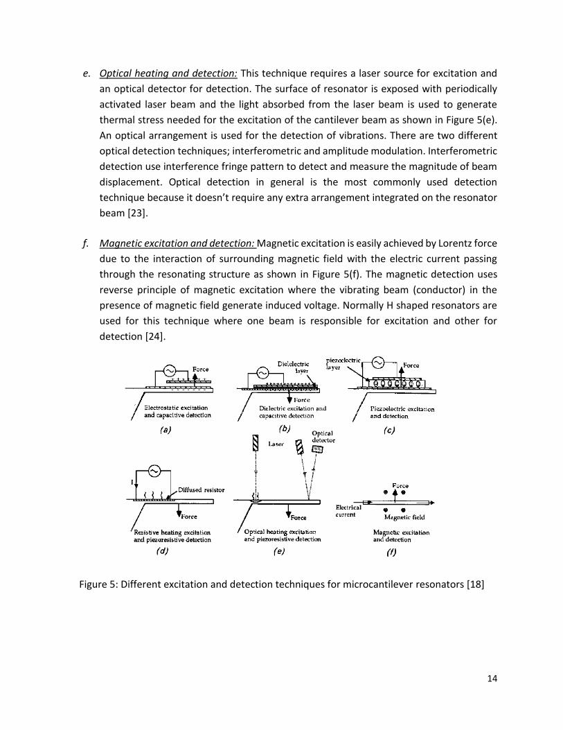
There are six most commonly used excitation techniques along with their corresponding
detection methods in order to investigate vibrations of a resonator structure.
a. Electrostatic excitation and capacitive detection: This technique requires two electrodes
place very close to each other to make a parallel plat capacitor where one electrode is the
part of cantilever beam as shown in Figure 5(a). The two electrodes are separated by an
air gap. When an alternating voltage is applied to the electrodes, the generated
(2)
13
electrostatic force will have a pulling effect resulting in the deflection of the cantilever
beam. The detection technique also makes use of the same electrodes. The vibration of
the beam changes the distance between the electrodes resulting in the change in
capacitance that can be used to detect vibration of the beam. This excitation technique is
very effective where resonator oscillates in vacuum in order to avoid air damping [19].
b. Dielectric excitation and capacitive detection: This technique is very similar to the above
mentioned technique except that a very thin layer of dielectric layer is sandwiched
between two electrodes where one electrode is the part of the cantilever beam as shown
in Figure 5(b). AC voltage creates electrostatic force which laterally deforms the dielectric
thin film. This deformation generates a bending moment in the beam. Vibrations cause
the area between the plates to change resulting in change in capacitance, which is used
to detect beam vibration [20].
c. Piezoelectric excitation and detection: This technique makes use of a piezoelectric
material such as ZnO or AIN for excitation and detection of beam vibrations. When voltage
is applied across piezoelectric material, it undergoes physical deformation which is used
to excite resonators. The top surface of the beam is deposited with a pair of electrodes
where piezoelectric material is sandwiched in between as shown in Figure 5(c). When an
AC voltage is applied to the electrodes then stress is generated in the piezoelectric layer
resulting in bending of the cantilever. The reverse piezoelectricity can be used for
detection of beam vibration. Vibrating beam cause physical deformation of the
piezoelectric layer that generates electric field across it and by measuring this electric
field, the magnitude of vibration can be measured [21].
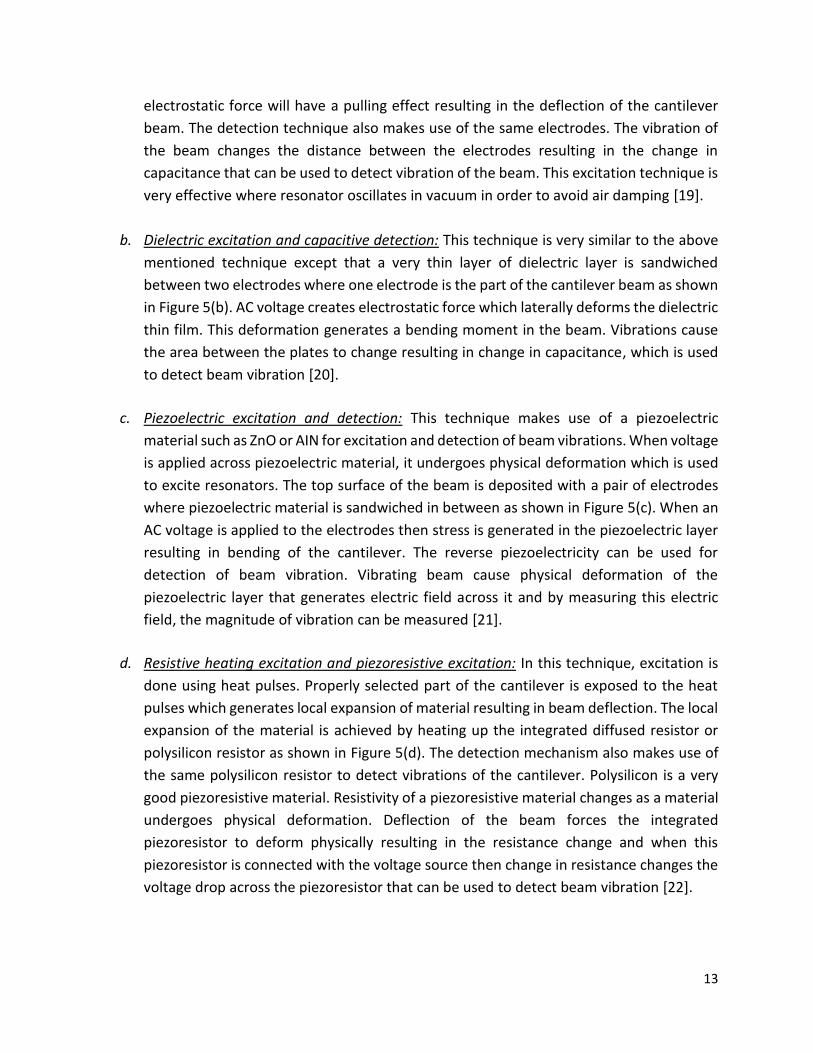
d. Resistive heating excitation and piezoresistive excitation: In this technique, excitation is
done using heat pulses. Properly selected part of the cantilever is exposed to the heat
pulses which generates local expansion of material resulting in beam deflection. The local
expansion of the material is achieved by heating up the integrated diffused resistor or
polysilicon resistor as shown in Figure 5(d). The detection mechanism also makes use of
the same polysilicon resistor to detect vibrations of the cantilever. Polysilicon is a very
good piezoresistive material. Resistivity of a piezoresistive material changes as a material
undergoes physical deformation. Deflection of the beam forces the integrated
piezoresistor to deform physically resulting in the resistance change and when this
piezoresistor is connected with the voltage source then change in resistance changes the
voltage drop across the piezoresistor that can be used to detect beam vibration [22].
14
e. Optical heating and detection: This technique requires a laser source for excitation and
an optical detector for detection. The surface of resonator is exposed with periodically
activated laser beam and the light absorbed from the laser beam is used to generate
thermal stress needed for the excitation of the cantilever beam as shown in Figure 5(e).
An optical arrangement is used for the detection of vibrations. There are two different
optical detection techniques; interferometric and amplitude modulation. Interferometric
detection use interference fringe pattern to detect and measure the magnitude of beam
displacement. Optical detection in general is the most commonly used detection
technique because it doesn’t require any extra arrangement integrated on the resonator
beam [23].
f. Magnetic excitation and detection: Magnetic excitation is easily achieved by Lorentz force
due to the interaction of surrounding magnetic field with the electric current passing
through the resonating structure as shown in Figure 5(f). The magnetic detection uses
reverse principle of magnetic excitation where the vibrating beam (conductor) in the
presence of magnetic field generate induced voltage. Normally H shaped resonators are
used for this technique where one beam is responsible for excitation and other for
detection [24].
Figure 5: Different excitation and detection techniques for microcantilever resonators [18]
15
1.3.3. Applications of Microcantilever Resonators
Resonators are used today in most of the MEMS devices such as inertial sensors, bio sensors,
chemical sensors, pressure sensors and energy harvesters. Cantilever is one of the simplest and
commonly used resonator structure. Below are a few application areas of MEMS resonators.
1.3.3.1. Mass sensor
Microcantilever based mass sensors are used to detect minimal changes in mass attached to the
surface of the cantilever. Due to the simple geometry of cantilevers, extreme miniaturization and
enhanced mass sensitivity can be achieved. MEMS mass sensors have the capability to detect
mass changes even below picogram level [25]. The detection is based on the change in resonance
frequency or stress induced bending. In static mode, sensing is done due to the change in surface
stress generated as the mass is attached on the surface of the cantilever whereas sensing in
dynamic mode depends on the change in resonance frequency [26]. Dynamic mode of operation
for mass sensing is more preferable due to sensitivity and long term stability. By using the same
principle, there are many different applications where MEMS mass sensors can be used to
investigate different types of molecules or gases present in the surrounding environment [27].
1.3.3.2. Chemical Sensor
Chemical sensors have found many applications in environmental monitoring for the detection
and quantification of potentially dangerous gasses [28] and in biomedical applications [29].
Current methods for the detection of chemical contamination are gas/liquid chromatography
and mass spectroscopy, which are relatively expensive and time consuming. On the other hand,
MEMS chemical sensors are cheaper, faster and can be integrated with wireless communication
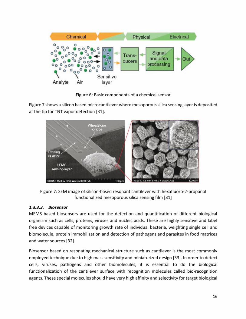
circuitry for rapid response. The basic components of a MEMS chemical sensor consist of a
sensitive layer which binds with molecules of interest from the surrounding environment as
shown in Figure 6. This sensitive layer can be a polymer for chemical sensing and antibodies for
bio-chemical sensing. It is very important that sensitive layer should have very high affinity for
the molecules of interest and very low affinity for other substances. The second main component
of a MEMS chemical sensor is a transducer that detects the binding of molecules with the
sensitive layer and convert it into a readable signal that can be processed by signal processing
unit and later can be used by other devices in the system [30].
16
Figure 6: Basic components of a chemical sensor
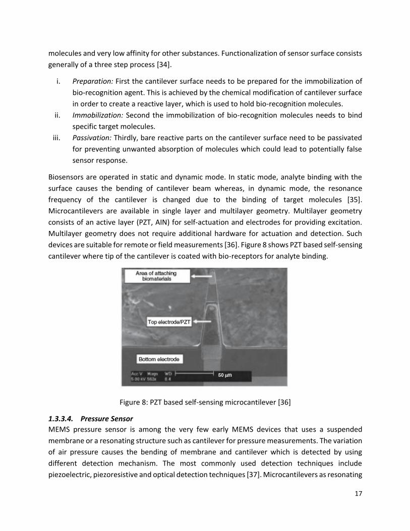
Figure 7 shows a silicon based microcantilever where mesoporous silica sensing layer is deposited
at the tip for TNT vapor detection [31].
Figure 7: SEM image of silicon-based resonant cantilever with hexafluoro-2-propanol functionalized mesoporous silica sensing film [31]
1.3.3.3. Biosensor
MEMS based biosensors are used for the detection and quantification of different biological
organism such as cells, proteins, viruses and nucleic acids. These are highly sensitive and label
free devices capable of monitoring growth rate of individual bacteria, weighting single cell and
biomolecule, protein immobilization and detection of pathogens and parasites in food matrices
and water sources [32].
Biosensor based on resonating mechanical structure such as cantilever is the most commonly
employed technique due to high mass sensitivity and miniaturized design [33]. In order to detect
cells, viruses, pathogens and other biomolecules, it is essential to do the biological
functionalization of the cantilever surface with recognition molecules called bio-recognition
agents. These special molecules should have very high affinity and selectivity for target biological
17
molecules and very low affinity for other substances. Functionalization of sensor surface consists
generally of a three step process [34].
i. Preparation: First the cantilever surface needs to be prepared for the immobilization of
bio-recognition agent. This is achieved by the chemical modification of cantilever surface
in order to create a reactive layer, which is used to hold bio-recognition molecules.
ii. Immobilization: Second the immobilization of bio-recognition molecules needs to bind
specific target molecules.
iii. Passivation: Thirdly, bare reactive parts on the cantilever surface need to be passivated
for preventing unwanted absorption of molecules which could lead to potentially false
sensor response.
Biosensors are operated in static and dynamic mode. In static mode, analyte binding with the
surface causes the bending of cantilever beam whereas, in dynamic mode, the resonance
frequency of the cantilever is changed due to the binding of target molecules [35].
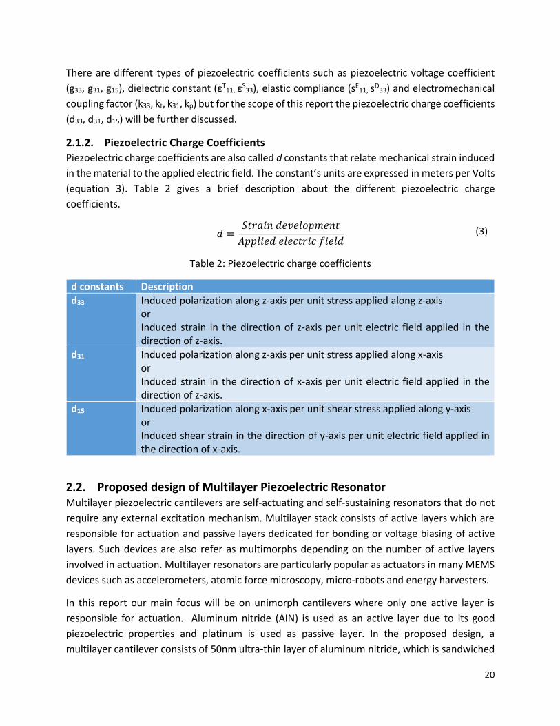
Microcantilevers are available in single layer and multilayer geometry. Multilayer geometry
consists of an active layer (PZT, AIN) for self-actuation and electrodes for providing excitation.
Multilayer geometry does not require additional hardware for actuation and detection. Such
devices are suitable for remote or field measurements [36]. Figure 8 shows PZT based self-sensing
cantilever where tip of the cantilever is coated with bio-receptors for analyte binding.
Figure 8: PZT based self-sensing microcantilever [36]
1.3.3.4. Pressure Sensor
MEMS pressure sensor is among the very few early MEMS devices that uses a suspended
membrane or a resonating structure such as cantilever for pressure measurements. The variation
of air pressure causes the bending of membrane and cantilever which is detected by using
different detection mechanism. The most commonly used detection techniques include
piezoelectric, piezoresistive and optical detection techniques [37]. Microcantilevers as resonating

18
structures have been the focus of studies for many years. Microcantilever sensors can be used to
detect the variation of surrounding pressure due to the change in resonance frequency or change
in damping conditions [38]. In changing pressure environment, a vibrating cantilever beam
behaves like a damped oscillator where the damping is the function of surrounding pressure [39].
The damping is caused by the interaction of surrounding gas or fluid molecules with the cantilever
surface which leads to the dissipation and eventually the resonance frequency and the Q factor
of the cantilever is degraded. By detecting this change in resonance frequency and quality factor
the surrounding pressure can be measured [40].

19
Chapter 2: Multilayer Piezoelectric NEMS Resonator
2.1. Piezoelectricity Piezoelectricity defines the ability of certain materials to develop electric charge in response to
the applied mechanical stress. Piezoelectricity provides a transduction mechanism to convert
electrical energy into mechanical motion. One of the unique property of piezoelectric materials
is to have converse effect. Converse piezoelectric effect is generation of strain in response to
applied electric field.
The piezoelectric effect is generated due to the occurrence of dipole moment in crystals. Crystals
of piezoelectric material (quartz, PZT, AIN etc.) are electrically neutral under no external force.
These crystals don’t have to be symmetrical but the atoms are arranged in such a way that
positive charges in one place cancel the effect of negative changes in the nearby place. When
piezoelectric material is squeezed or stretched or it comes under the influence of any type of
physical force, the structure gets deformed which leads to the unbalance between positive and
negative changes causing electrical charge to appear. Similarly, when an external electrical field
is applied, strain is induced in the crystals and atoms have to rearrange themselves in order to
release this strain resulting in physical deformation [41].
2.1.1. Piezoelectric Coefficients Piezoelectric coefficients create a link between electrical stimulus and mechanical response or
vice versa. They are used to quantify the volume change when electric field is applied on
piezoelectric material or it gives an indication of direction of polarization of piezoelectric material
when it is subject to external stress. Each coefficient, as a second-rank tensor, is described by its
two subscripts. First subscript represents the direction of polarization whereas the second
subscript represents the direction of induced stress. By convention, direction along X, Y and Z is
represented by subscript 1, 2 and 3 respectively and shear about axis X, Y and Z is represented
by the subscript 4, 5, or 6 respectively as shown in Figure 9.
Figure 9: Direction of forces affecting a piezoelectric element
20
There are different types of piezoelectric coefficients such as piezoelectric voltage coefficient
(g33, g31, g15), dielectric constant (εT11, εS
33), elastic compliance (sE11, sD
33) and electromechanical
coupling factor (k33, kt, k31, kp) but for the scope of this report the piezoelectric charge coefficients
(d33, d31, d15) will be further discussed.
2.1.2. Piezoelectric Charge Coefficients
Piezoelectric charge coefficients are also called d constants that relate mechanical strain induced
in the material to the applied electric field. The constant’s units are expressed in meters per Volts
(equation 3). Table 2 gives a brief description about the different piezoelectric charge
coefficients.
𝑑 =𝑆𝑡𝑟𝑎𝑖𝑛 𝑑𝑒𝑣𝑒𝑙𝑜𝑝𝑚𝑒𝑛𝑡
𝐴𝑝𝑝𝑙𝑖𝑒𝑑 𝑒𝑙𝑒𝑐𝑡𝑟𝑖𝑐 𝑓𝑖𝑒𝑙𝑑
Table 2: Piezoelectric charge coefficients
d constants Description
d33 Induced polarization along z-axis per unit stress applied along z-axis or Induced strain in the direction of z-axis per unit electric field applied in the direction of z-axis.
d31 Induced polarization along z-axis per unit stress applied along x-axis or Induced strain in the direction of x-axis per unit electric field applied in the direction of z-axis.
d15 Induced polarization along x-axis per unit shear stress applied along y-axis or Induced shear strain in the direction of y-axis per unit electric field applied in the direction of x-axis.
2.2. Proposed design of Multilayer Piezoelectric Resonator Multilayer piezoelectric cantilevers are self-actuating and self-sustaining resonators that do not
require any external excitation mechanism. Multilayer stack consists of active layers which are
responsible for actuation and passive layers dedicated for bonding or voltage biasing of active
layers. Such devices are also refer as multimorphs depending on the number of active layers
involved in actuation. Multilayer resonators are particularly popular as actuators in many MEMS
devices such as accelerometers, atomic force microscopy, micro-robots and energy harvesters.
In this report our main focus will be on unimorph cantilevers where only one active layer is
responsible for actuation. Aluminum nitride (AIN) is used as an active layer due to its good
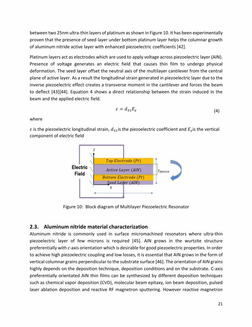
piezoelectric properties and platinum is used as passive layer. In the proposed design, a
multilayer cantilever consists of 50nm ultra-thin layer of aluminum nitride, which is sandwiched
(3)
21
between two 25nm ultra-thin layers of platinum as shown in Figure 10. It has been experimentally
proven that the presence of seed layer under bottom platinum layer helps the columnar growth
of aluminum nitride active layer with enhanced piezoelectric coefficients [42].
Platinum layers act as electrodes which are used to apply voltage across piezoelectric layer (AIN).
Presence of voltage generates an electric field that causes thin film to undergo physical
deformation. The seed layer offset the neutral axis of the multilayer cantilever from the central
plane of active layer. As a result the longitudinal strain generated in piezoelectric layer due to the
inverse piezoelectric effect creates a transverse moment in the cantilever and forces the beam
to deflect [43][44]. Equation 4 shows a direct relationship between the strain induced in the
beam and the applied electric field.
𝜀 = 𝑑31𝐸𝑧
where
𝜀 is the piezoelectric longitudinal strain, 𝑑31is the piezoelectric coefficient and 𝐸𝑧is the vertical
component of electric field
Figure 10: Block diagram of Multilayer Piezoelectric Resonator
2.3. Aluminum nitride material characterization Aluminum nitride is commonly used in surface micromachined resonators where ultra-thin
piezoelectric layer of few microns is required [45]. AIN grows in the wurtzite structure
preferentially with c-axis orientation which is desirable for good piezoelectric properties. In order
to achieve high piezoelectric coupling and low losses, it is essential that AIN grows in the form of
vertical columnar grains perpendicular to the substrate surface [46]. The orientation of AIN grains
highly depends on the deposition technique, deposition conditions and on the substrate. C-axis
preferentially orientated AIN thin films can be synthesized by different deposition techniques
such as chemical vapor deposition (CVD), molecular beam epitaxy, ion beam deposition, pulsed
laser ablation deposition and reactive RF magnetron sputtering. However reactive magnetron
(4)
22
sputtering is the most favorable choice for deposition of AIN films due to reproducibility, low cost
and low deposition temperature requirement (300-450 0C) which also makes it compatible with
Integrated Circuit (IC) fabrication [47].
2.3.1. DC Pulsed reactive magnetron sputtering for AIN thin films Reactive sputtering is a physical vapor deposition (PVD) process for deposition of thin films by
sputtering the material from target and depositing it on the substrate. Sputtering of target
material is done by the bombardment of high energy ions or atoms of some gas especially inert
gas such as argon. Some additional gases are also introduced in the chamber along with argon
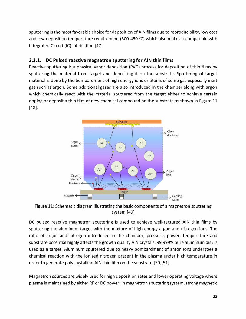
which chemically react with the material sputtered from the target either to achieve certain
doping or deposit a thin film of new chemical compound on the substrate as shown in Figure 11
[48].
Figure 11: Schematic diagram illustrating the basic components of a magnetron sputtering
system [49]
DC pulsed reactive magnetron sputtering is used to achieve well-textured AIN thin films by
sputtering the aluminum target with the mixture of high energy argon and nitrogen ions. The
ratio of argon and nitrogen introduced in the chamber, pressure, power, temperature and
substrate potential highly affects the growth quality AIN crystals. 99.999% pure aluminum disk is
used as a target. Aluminum sputtered due to heavy bombardment of argon ions undergoes a
chemical reaction with the ionized nitrogen present in the plasma under high temperature in
order to generate polycrystalline AIN thin film on the substrate [50][51].
Magnetron sources are widely used for high deposition rates and lower operating voltage where
plasma is maintained by either RF or DC power. In magnetron sputtering system, strong magnetic
23
field is generated near the target area which causes the electrons to spiral along the magnetic
flux line near the target. This arrangement is used to confine plasma in front of the target area in
order to intensify the bombardment of ions. As a result, a highly dense plasma is achieved [49].
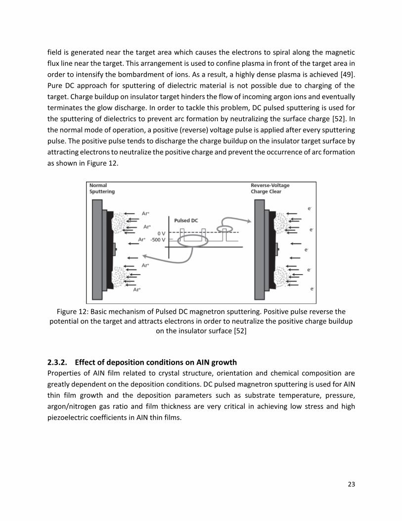
Pure DC approach for sputtering of dielectric material is not possible due to charging of the
target. Charge buildup on insulator target hinders the flow of incoming argon ions and eventually
terminates the glow discharge. In order to tackle this problem, DC pulsed sputtering is used for
the sputtering of dielectrics to prevent arc formation by neutralizing the surface charge [52]. In
the normal mode of operation, a positive (reverse) voltage pulse is applied after every sputtering
pulse. The positive pulse tends to discharge the charge buildup on the insulator target surface by
attracting electrons to neutralize the positive charge and prevent the occurrence of arc formation
as shown in Figure 12.
Figure 12: Basic mechanism of Pulsed DC magnetron sputtering. Positive pulse reverse the
potential on the target and attracts electrons in order to neutralize the positive charge buildup on the insulator surface [52]
2.3.2. Effect of deposition conditions on AIN growth Properties of AIN film related to crystal structure, orientation and chemical composition are
greatly dependent on the deposition conditions. DC pulsed magnetron sputtering is used for AIN
thin film growth and the deposition parameters such as substrate temperature, pressure,
argon/nitrogen gas ratio and film thickness are very critical in achieving low stress and high
piezoelectric coefficients in AIN thin films.
24
2.3.2.1. Substrate Temperature
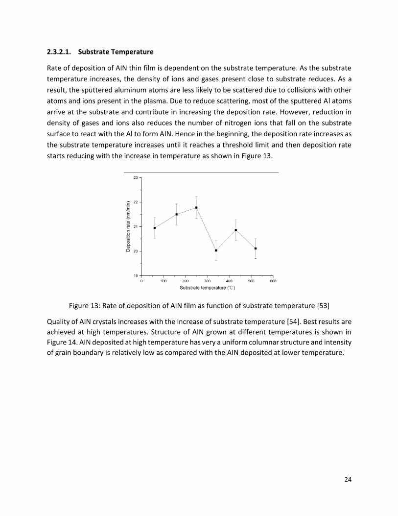
Rate of deposition of AIN thin film is dependent on the substrate temperature. As the substrate
temperature increases, the density of ions and gases present close to substrate reduces. As a
result, the sputtered aluminum atoms are less likely to be scattered due to collisions with other
atoms and ions present in the plasma. Due to reduce scattering, most of the sputtered Al atoms
arrive at the substrate and contribute in increasing the deposition rate. However, reduction in
density of gases and ions also reduces the number of nitrogen ions that fall on the substrate
surface to react with the Al to form AIN. Hence in the beginning, the deposition rate increases as
the substrate temperature increases until it reaches a threshold limit and then deposition rate
starts reducing with the increase in temperature as shown in Figure 13.
Figure 13: Rate of deposition of AIN film as function of substrate temperature [53]
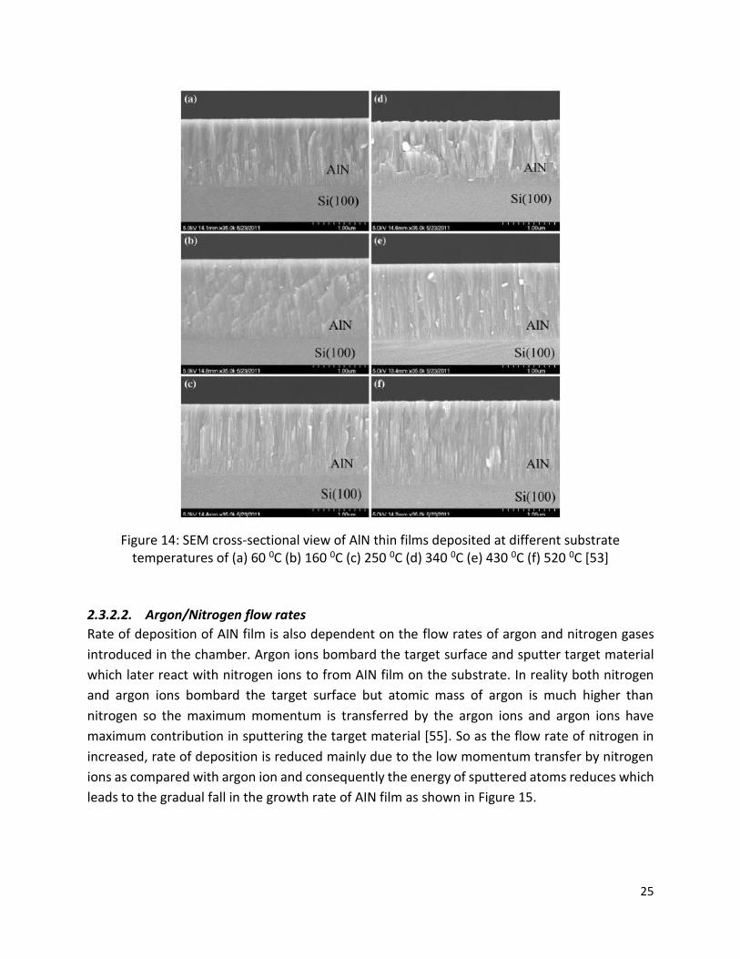
Quality of AIN crystals increases with the increase of substrate temperature [54]. Best results are
achieved at high temperatures. Structure of AIN grown at different temperatures is shown in
Figure 14. AIN deposited at high temperature has very a uniform columnar structure and intensity
of grain boundary is relatively low as compared with the AIN deposited at lower temperature.
25
Figure 14: SEM cross-sectional view of AlN thin films deposited at different substrate temperatures of (a) 60 0C (b) 160 0C (c) 250 0C (d) 340 0C (e) 430 0C (f) 520 0C [53]
2.3.2.2. Argon/Nitrogen flow rates
Rate of deposition of AIN film is also dependent on the flow rates of argon and nitrogen gases
introduced in the chamber. Argon ions bombard the target surface and sputter target material
which later react with nitrogen ions to from AIN film on the substrate. In reality both nitrogen
and argon ions bombard the target surface but atomic mass of argon is much higher than
nitrogen so the maximum momentum is transferred by the argon ions and argon ions have
maximum contribution in sputtering the target material [55]. So as the flow rate of nitrogen in
increased, rate of deposition is reduced mainly due to the low momentum transfer by nitrogen
ions as compared with argon ion and consequently the energy of sputtered atoms reduces which
leads to the gradual fall in the growth rate of AIN film as shown in Figure 15.
26
Figure 15: AIN film deposition rate for different nitrogen flow rates [55]
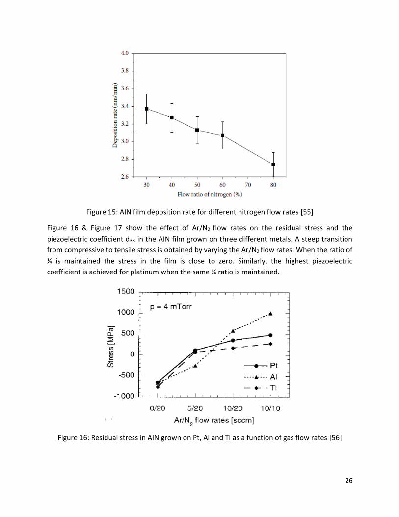
Figure 16 & Figure 17 show the effect of Ar/N2 flow rates on the residual stress and the
piezoelectric coefficient d33 in the AIN film grown on three different metals. A steep transition
from compressive to tensile stress is obtained by varying the Ar/N2 flow rates. When the ratio of
¼ is maintained the stress in the film is close to zero. Similarly, the highest piezoelectric
coefficient is achieved for platinum when the same ¼ ratio is maintained.
Figure 16: Residual stress in AIN grown on Pt, Al and Ti as a function of gas flow rates [56]
27
Figure 17: Piezoelectric coefficient d33 of AIN grown on Pt, Al and Ti as a function of gas flow
rates [56]
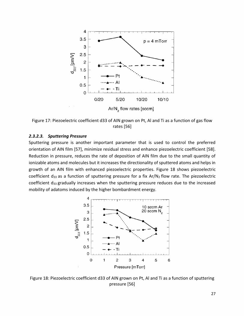
2.3.2.3. Sputtering Pressure
Sputtering pressure is another important parameter that is used to control the preferred
orientation of AIN film [57], minimize residual stress and enhance piezoelectric coefficient [58].
Reduction in pressure, reduces the rate of deposition of AIN film due to the small quantity of
ionizable atoms and molecules but it increases the directionality of sputtered atoms and helps in
growth of an AIN film with enhanced piezoelectric properties. Figure 18 shows piezoelectric
coefficient d33 as a function of sputtering pressure for a fix Ar/N2 flow rate. The piezoelectric
coefficient d33 gradually increases when the sputtering pressure reduces due to the increased
mobility of adatoms induced by the higher bombardment energy.
Figure 18: Piezoelectric coefficient d33 of AIN grown on Pt, Al and Ti as a function of sputtering
pressure [56]

28
Figure 19 shows the effect of sputtering pressure on the residual stress generated in the AIN film.
A steep transition from tensile to compressive stress is observed with the increase in pressure
due to the bombardment of growing layer with the high energy plasma species. Bombardment
energy depends on the collisions among atoms and ions before they reach the substrate. At low
pressure, accelerated ions suffer few collisions in the plasma and their interaction with substrate
surface is almost perpendicular. Due to the high directionality of ionic bombardment, higher
residual stress is generated [59]. Sputtering pressure should be controlled very carefully in order
to achieve low stress and high piezoelectric response. The energy of the ions should be high
enough to grow well-textured AIN film but not too high that the bombardment deteriorates the
crystal quality.
Figure 19: Residual stress of AIN grown on Pt, Al and Ti as a function of sputtering pressure [56]
2.3.3. Platinum electrode layer for AIN thin film growth
Quality of AIN film is greatly influenced by the nature of the electrode material. Among other
metals (Al, Ti etc.) platinum gives the best results in term of low residual stress and high
piezoelectric coefficient as shown in Figures 16, 17, 18 & 19. Platinum with (111) orientation is
favorable for the growth of (0002) oriented AIN film. AIN is deposited on top of the platinum
which serves as the bottom electrode. Bottom platinum electrode not only helps to grow well
textured c-oriented AIN films but it is also used to apply voltage across piezoelectric (AIN) layer.
For thick AIN films, the residual stress contribution from platinum electrode is only dependent
on the deposition conditions rather than the material itself [60]. The AIN in-plane lattice constant
is 12% larger than the Pt-Pt distance on the (111) plane which is not an issue for the thicker AIN
films. Figure 20 shows a steep transition from compressive to tensile stress as the thickness of
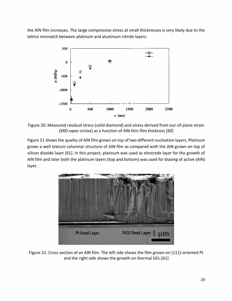
29
the AIN film increases. The large compressive stress at small thicknesses is very likely due to the
lattice mismatch between platinum and aluminum nitride layers.
Figure 20: Measured residual stress (solid diamond) and stress derived from out-of-plane strain (XRD-open circles) as a function of AlN thin-film thickness [60]
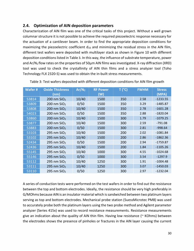
Figure 21 shows the quality of AIN film grown on top of two different nucleation layers. Platinum
grows a well texture columnar structure of AIN film as compared with the AIN grown on top of
silicon dioxide layer [61]. In this project, platinum was used as electrode layer for the growth of
AIN film and later both the platinum layers (top and bottom) was used for biasing of active (AIN)
layer.
Figure 21: Cross section of an AlN film. The left side shows the film grown on (111)-oriented Pt and the right side shows the growth on thermal SiO2 [61]
30
2.4. Optimization of AIN deposition parameters Characterization of AIN film was one of the critical tasks of this project. Without a well grown
columnar structure it is not possible to achieve the required piezoelectric response necessary for
the actuation of a cantilever beam. In order to find the appropriate deposition conditions for
maximizing the piezoelectric coefficient d33 and minimizing the residual stress in the AIN film,
different test wafers were deposited with multilayer stack as shown in Figure 10 with different
deposition conditions listed in Table 3. In this way, the influence of substrate temperature, power
and Ar/N2 flow rates on the properties of 50µm AIN films was investigated. X-ray diffraction (XRD)
tool was used to check the crystallinity of AIN thin films and a stress analyzer tool (Toho
Technology FLX 2320-S) was used to obtain the in-built stress measurements.
Table 3: Test wafers deposited with different deposition conditions for AIN film growth
Wafer # Oxide Thickness (nm)
Ar/N2 RF Power (W)
T (°C) FWHM Stress (MPA)
53814 200 nm SiO2 10/40 1500 350 2.58 -1233.55
53809 200 nm SiO2 0/50 1500 350 3.29 -1485.87
53808 200 nm SiO2 10/40 1500 350 2.78 -1601.28
54023 200 nm SiO2 0/50 1500 350 2.88 -1820.04
53860 200 nm SiO2 10/40 1500 300 1.79 -1079.25
53877 200 nm SiO2 10/40 1500 300 2.59 -791.08
53883 200 nm SiO2 0/50 1500 300 2.81 -998.64
53103 295 nm SiO2 10/40 1500 200 2.02 -1081.84
53102 295 nm SiO2 10/40 1500 200 2.86 -1862.36
52434 295 nm SiO2 0/50 1500 200 2.94 -1759.87
52436 295 nm SiO2 10/40 1500 200 1.84 -1105.26
55145 295 nm SiO2 10/40 1000 300 4.55 -1024.68
55146 295 nm SiO2 0/50 1000 300 3.54 -1297.9
53112 295 nm SiO2 10/40 1250 300 1.91 -1004.48
53111 295 nm SiO2 10/40 1250 300 3.07 -1450.03
53110 295 nm SiO2 0/50 1250 300 2.97 -1232.04
A series of conduction tests were performed on the test wafers in order to find out the resistance
between the top and bottom electrodes. Ideally, the resistance should be very high preferably in
G/MOhms because AIN is an insulator material which is sandwiched between two platinum layers
serving as top and bottom electrodes. Mechanical probe station (SuessMicrotec PM8) was used
to accurately probe both the platinum layers using the two probe method and Agilent parameter
analyzer (Series 415x) was used to record resistance measurements. Resistance measurements
give an indication about the quality of AIN thin film. Having low resistance (~ KOhms) between
the electrodes shows the presence of pinholes or fractures in the AIN layer causing the current
31
to leak and short circuit the electrodes. Short circuiting of electrodes does not allow to develop
a strong electric field across piezoelectric (AIN) layer which is necessary for the actuation causing
the device to fail.
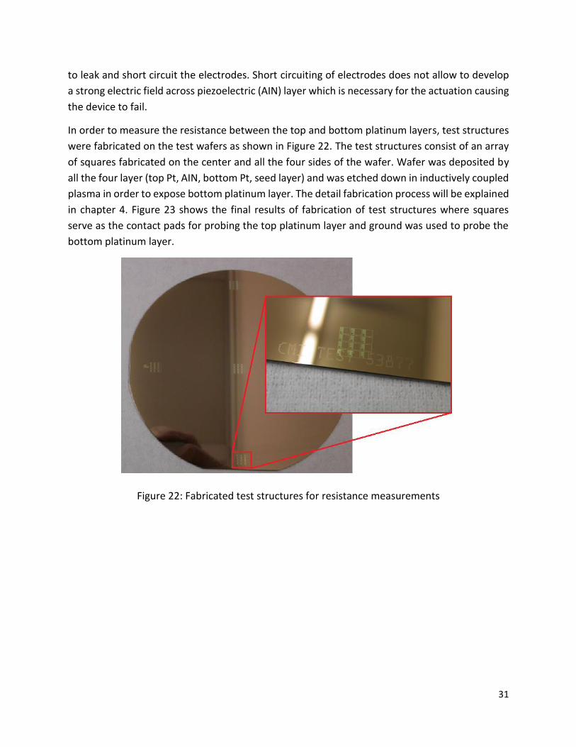
In order to measure the resistance between the top and bottom platinum layers, test structures
were fabricated on the test wafers as shown in Figure 22. The test structures consist of an array
of squares fabricated on the center and all the four sides of the wafer. Wafer was deposited by
all the four layer (top Pt, AIN, bottom Pt, seed layer) and was etched down in inductively coupled
plasma in order to expose bottom platinum layer. The detail fabrication process will be explained
in chapter 4. Figure 23 shows the final results of fabrication of test structures where squares
serve as the contact pads for probing the top platinum layer and ground was used to probe the
bottom platinum layer.
Figure 22: Fabricated test structures for resistance measurements
32
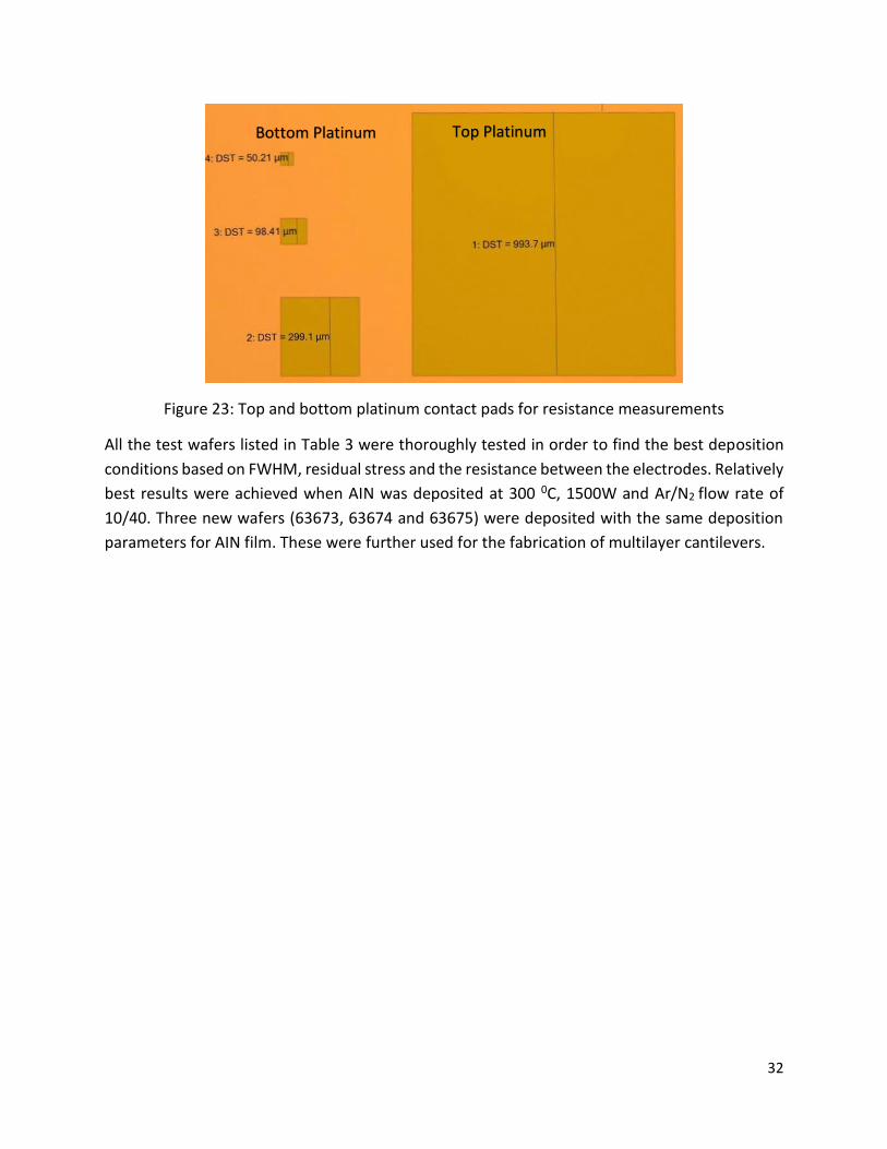
Figure 23: Top and bottom platinum contact pads for resistance measurements
All the test wafers listed in Table 3 were thoroughly tested in order to find the best deposition
conditions based on FWHM, residual stress and the resistance between the electrodes. Relatively
best results were achieved when AIN was deposited at 300 0C, 1500W and Ar/N2 flow rate of
10/40. Three new wafers (63673, 63674 and 63675) were deposited with the same deposition
parameters for AIN film. These were further used for the fabrication of multilayer cantilevers.
Top Platinum Bottom Platinum
33
Chapter 3: Finite element analysis of multilayer piezoelectric
resonators
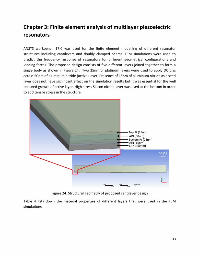
ANSYS workbench 17.0 was used for the finite element modelling of different resonator
structures including cantilevers and doubly clamped beams. FEM simulations were used to
predict the frequency response of resonators for different geometrical configurations and
loading forces. The proposed design consists of five different layers joined together to form a
single body as shown in Figure 24. Two 25nm of platinum layers were used to apply DC bias
across 50nm of aluminum nitride (active) layer. Presence of 15nm of aluminum nitride as a seed
layer does not have significant effect on the simulation results but it was essential for the well
textured growth of active layer. High stress Silicon nitride layer was used at the bottom in order
to add tensile stress in the structure.
Figure 24: Structural geometry of proposed cantilever design
Table 4 lists down the material properties of different layers that were used in the FEM
simulations.
Si3N4 (50nm) AIN (15nm) Bottom Pt (25nm) AIN (50nm) Top Pt (25nm)
34
Table 4: Material properties for FEM
Material Density (Kg/m3) Young’s Modulus (GPa) Poisson’s Ratio
AIN 3230 345 0.3
Pt 21440 170 0.39
Si3N4 3184 265 0.27
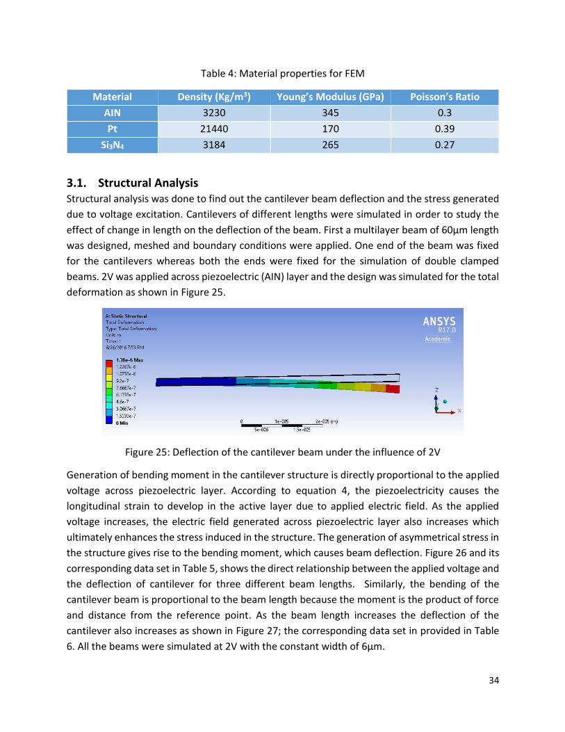
3.1. Structural Analysis Structural analysis was done to find out the cantilever beam deflection and the stress generated
due to voltage excitation. Cantilevers of different lengths were simulated in order to study the
effect of change in length on the deflection of the beam. First a multilayer beam of 60µm length
was designed, meshed and boundary conditions were applied. One end of the beam was fixed
for the cantilevers whereas both the ends were fixed for the simulation of double clamped
beams. 2V was applied across piezoelectric (AIN) layer and the design was simulated for the total
deformation as shown in Figure 25.
Figure 25: Deflection of the cantilever beam under the influence of 2V
Generation of bending moment in the cantilever structure is directly proportional to the applied
voltage across piezoelectric layer. According to equation 4, the piezoelectricity causes the
longitudinal strain to develop in the active layer due to applied electric field. As the applied
voltage increases, the electric field generated across piezoelectric layer also increases which
ultimately enhances the stress induced in the structure. The generation of asymmetrical stress in
the structure gives rise to the bending moment, which causes beam deflection. Figure 26 and its
corresponding data set in Table 5, shows the direct relationship between the applied voltage and
the deflection of cantilever for three different beam lengths. Similarly, the bending of the
cantilever beam is proportional to the beam length because the moment is the product of force
and distance from the reference point. As the beam length increases the deflection of the
cantilever also increases as shown in Figure 27; the corresponding data set in provided in Table
6. All the beams were simulated at 2V with the constant width of 6µm.
35
Figure 26: Relationship between cantilever bending and applied potential for three different beam lengths
Table 5: Simulated results of cantilever deflection expressed in microns for different applied voltages
DC Bias (V) 60µm 54µm 48µm
0 0 0 0
1 0.69 0.56 0.45
2 1.4 1.1 0.89
3 2.1 1.7 1.3
4 2.8 2.2 1.8
0.0E+00
5.0E-07
1.0E-06
1.5E-06
2.0E-06
2.5E-06
3.0E-06
0 0.5 1 1.5 2 2.5 3 3.5 4 4.5
Bea
m D
flec
tio
n (
m)
DC Bias (V)
Beam Deflection Vs Applied Voltage
60µm 54µm 48µm
0.0E+00
2.0E-07
4.0E-07
6.0E-07
8.0E-07
1.0E-06
1.2E-06
1.4E-06
1.6E-06
0 10 20 30 40 50 60 70
Bea
m D
efle
ctio
n (
m)
Beam Length (µm)
Beam Deflection Vs Beam Length

36
Figure 27: Deflection of cantilever for different beam lengths
Table 6: Data set for cantilever deflection expressed in microns for different beam lengths
Length (µm) Deflection (µm)
60 1.4
54 1.1
48 0.89
42 0.68
36 0.51
30 0.35
24 0.23
18 0.13
12 0.062
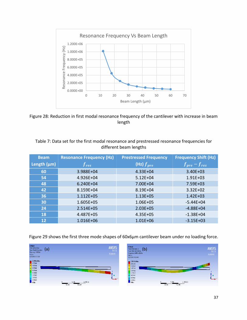
3.2. Modal Analysis Modal analysis was carried out to find the resonance frequency and the mode shapes of
cantilever for different lengths. The effect of applied voltage on the change in resonance
frequency was also studied. Resonance frequency is inversely proportional to the square of
length of the beam as shown in equation 5. The same behavior was achieved when a 6µm wide
cantilever was simulated over the range of different lengths to find out the resonance frequency
of the first mode as shown in Figure 28 and in its corresponding data set in Table 7.
𝑓𝑟𝑒𝑠 =(1.875)2
2𝜋√
𝐸𝐼
𝜌𝐴𝐿4
where E is Young’s Modulus, I is moment of inertia, 𝜌 is material density, A is area of cross section
and L is the length of the cantilever beam.
Stress generated in piezoelectric layer due to applied voltage also changes the resonance
frequency of the vibrating structure. Application of surface stress induces an axial force along the
length of the beam and the cantilever vibrates with the shifted resonance frequency [62]. Pre-
stress analysis of the cantilever was done in order to find the shift in resonance frequency due to
applied voltage. First the stress in the cantilever due to applied voltage was simulated and then
the generated stress was used as an input parameter for the modal analysis to calculate the
resonance frequency of the prestressed cantilever beam. Table 7 lists the shift in resonance
frequency values for different beam lengths at 5V.
(5)
37
Figure 28: Reduction in first modal resonance frequency of the cantilever with increase in beam length
Table 7: Data set for the first modal resonance and prestressed resonance frequencies for different beam lengths
Beam
Length (µm)
Resonance Frequency (Hz)
𝒇𝒓𝒆𝒔
Prestressed Frequency
(Hz) 𝒇𝒑𝒓𝒆
Frequency Shift (Hz)
𝒇𝒑𝒓𝒆 − 𝒇𝒓𝒆𝒔
60 3.988E+04 4.33E+04 3.40E+03
54 4.926E+04 5.12E+04 1.91E+03
48 6.240E+04 7.00E+04 7.59E+03
42 8.159E+04 8.19E+04 3.32E+02
36 1.112E+05 1.13E+05 1.42E+03
30 1.605E+05 1.06E+05 -5.44E+04
24 2.514E+05 2.03E+05 -4.88E+04
18 4.487E+05 4.35E+05 -1.38E+04
12 1.016E+06 1.01E+06 -3.15E+03
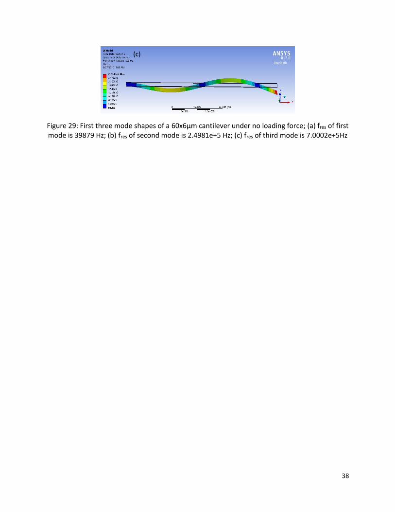
Figure 29 shows the first three mode shapes of 60x6µm cantilever beam under no loading force.
0.000E+00
2.000E+05
4.000E+05
6.000E+05
8.000E+05
1.000E+06
1.200E+06
0 10 20 30 40 50 60 70
Res
on
ance
Fre
qu
ency
(H
z)
Beam Length (µm)
Resonance Frequency Vs Beam Length
(a) (b)
38
Figure 29: First three mode shapes of a 60x6µm cantilever under no loading force; (a) fres of first mode is 39879 Hz; (b) fres of second mode is 2.4981e+5 Hz; (c) fres of third mode is 7.0002e+5Hz
(c)
39
Chapter 4: Fabrication
Device fabrication was carried out the in EPFL Cleanroom. Two different process flows were
implemented in order to achieve the desired results. In the first process flow, a bottom-up
approach was implemented. First only the seed and bottom platinum layers were deposited,
patterned and etched and afterwards the other two layers (AIN and top Pt layer) were deposited
and processed according to the first process flow. Unfortunately, the desired electrical insulation
between the top and the bottom platinum layers was not achieved due to the generation of high
fences on the sides of bottom platinum layer. In order to tackle this problem, a new process flow
was implemented with top-down approach where all the four layers (seed, bottom Pt, AIN and
top Pt layers) were deposited at once and etched downwards. The desired electrical insulation
between the top and bottom platinum layers was achieved which ultimately led to the successful
fabrication of multilayer cantilevers and doubly clamped beams.
In this chapter, the first process flow will be explained in detail along with the basic operation of
the machines used for the fabrication but the second process flow will be explained briefly except
the steps which have not been already discussed in the first process flow.

40
4.1. First Process Flow (a) Multilayer deposition of AIN, Pt and SiO2 (f) Dry Etching of SiO2, Pt & AIN in STS
(b) Photolithography of Bottom Pt Layer (g) Photolithography of Devices
(c) Dry Etching of SiO2 & Pt in IBE (h) Dry Etching of Pt & AIN in STS
(d) Multilayer deposition of AIN, Pt & SiO2 (i) Structure Releasing
(e) Photolithography of Top Pt Layer
Note:
The arrows indicate that AIN/Pt layers are connected out of present section plane.
Legend:
SiO2 Layer AIN Layer Pt Layer Photoresist Layer
41
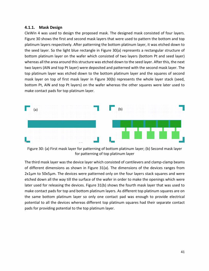
4.1.1. Mask Design
CleWin 4 was used to design the proposed mask. The designed mask consisted of four layers.
Figure 30 shows the first and second mask layers that were used to pattern the bottom and top
platinum layers respectively. After patterning the bottom platinum layer, it was etched down to
the seed layer. So the light blue rectangle in Figure 30(a) represents a rectangular structure of
bottom platinum layer on the wafer which consisted of two layers (bottom Pt and seed layer)
whereas all the area around this structure was etched down to the seed layer. After this, the next
two layers (AIN and top Pt layer) were deposited and patterned with the second mask layer. The
top platinum layer was etched down to the bottom platinum layer and the squares of second
mask layer on top of first mask layer in Figure 30(b) represents the whole layer stack (seed,
bottom Pt, AIN and top Pt layers) on the wafer whereas the other squares were later used to
make contact pads for top platinum layer.
Figure 30: (a) First mask layer for patterning of bottom platinum layer; (b) Second mask layer for patterning of top platinum layer
The third mask layer was the device layer which consisted of cantilevers and clamp-clamp beams
of different dimensions as shown in Figure 31(a). The dimensions of the devices ranges from
2x1µm to 50x5µm. The devices were patterned only on the four layers stack squares and were
etched down all the way till the surface of the wafer in order to make the openings which were
later used for releasing the devices. Figure 31(b) shows the fourth mask layer that was used to
make contact pads for top and bottom platinum layers. As different top platinum squares are on
the same bottom platinum layer so only one contact pad was enough to provide electrical
potential to all the devices whereas different top platinum squares had their separate contact
pads for providing potential to the top platinum layer.
(a) (b)
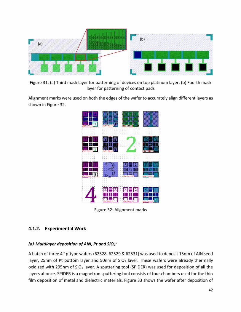
42
Figure 31: (a) Third mask layer for patterning of devices on top platinum layer; (b) Fourth mask layer for patterning of contact pads
Alignment marks were used on both the edges of the wafer to accurately align different layers as
shown in Figure 32.
Figure 32: Alignment marks
4.1.2. Experimental Work
(a) Multilayer deposition of AIN, Pt and SiO2:
A batch of three 4’’ p-type wafers (62528, 62529 & 62531) was used to deposit 15nm of AIN seed
layer, 25nm of Pt bottom layer and 50nm of SiO2 layer. These wafers were already thermally
oxidized with 295nm of SiO2 layer. A sputtering tool (SPIDER) was used for deposition of all the
layers at once. SPIDER is a magnetron sputtering tool consists of four chambers used for the thin
film deposition of metal and dielectric materials. Figure 33 shows the wafer after deposition of
(a) (b)
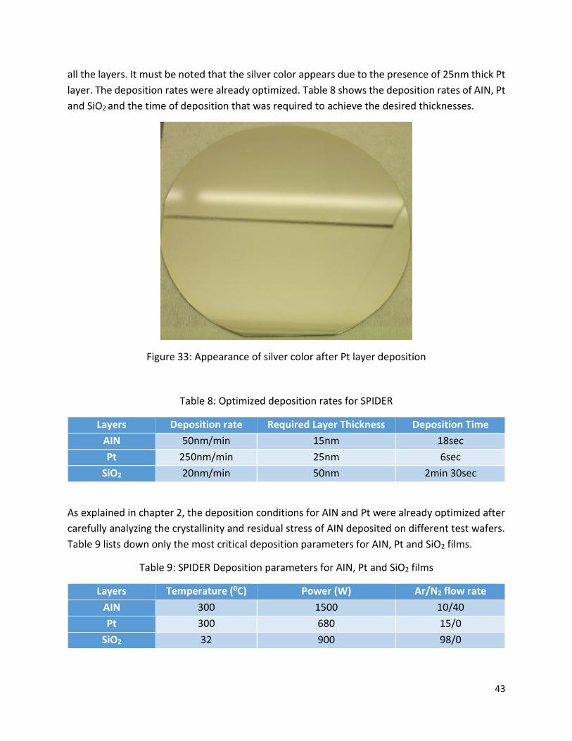
43
all the layers. It must be noted that the silver color appears due to the presence of 25nm thick Pt
layer. The deposition rates were already optimized. Table 8 shows the deposition rates of AIN, Pt
and SiO2 and the time of deposition that was required to achieve the desired thicknesses.
Figure 33: Appearance of silver color after Pt layer deposition
Table 8: Optimized deposition rates for SPIDER
Layers Deposition rate Required Layer Thickness Deposition Time
AIN 50nm/min 15nm 18sec
Pt 250nm/min 25nm 6sec
SiO2 20nm/min 50nm 2min 30sec
As explained in chapter 2, the deposition conditions for AIN and Pt were already optimized after
carefully analyzing the crystallinity and residual stress of AIN deposited on different test wafers.
Table 9 lists down only the most critical deposition parameters for AIN, Pt and SiO2 films.
Table 9: SPIDER Deposition parameters for AIN, Pt and SiO2 films
Layers Temperature (0C) Power (W) Ar/N2 flow rate
AIN 300 1500 10/40
Pt 300 680 15/0
SiO2 32 900 98/0
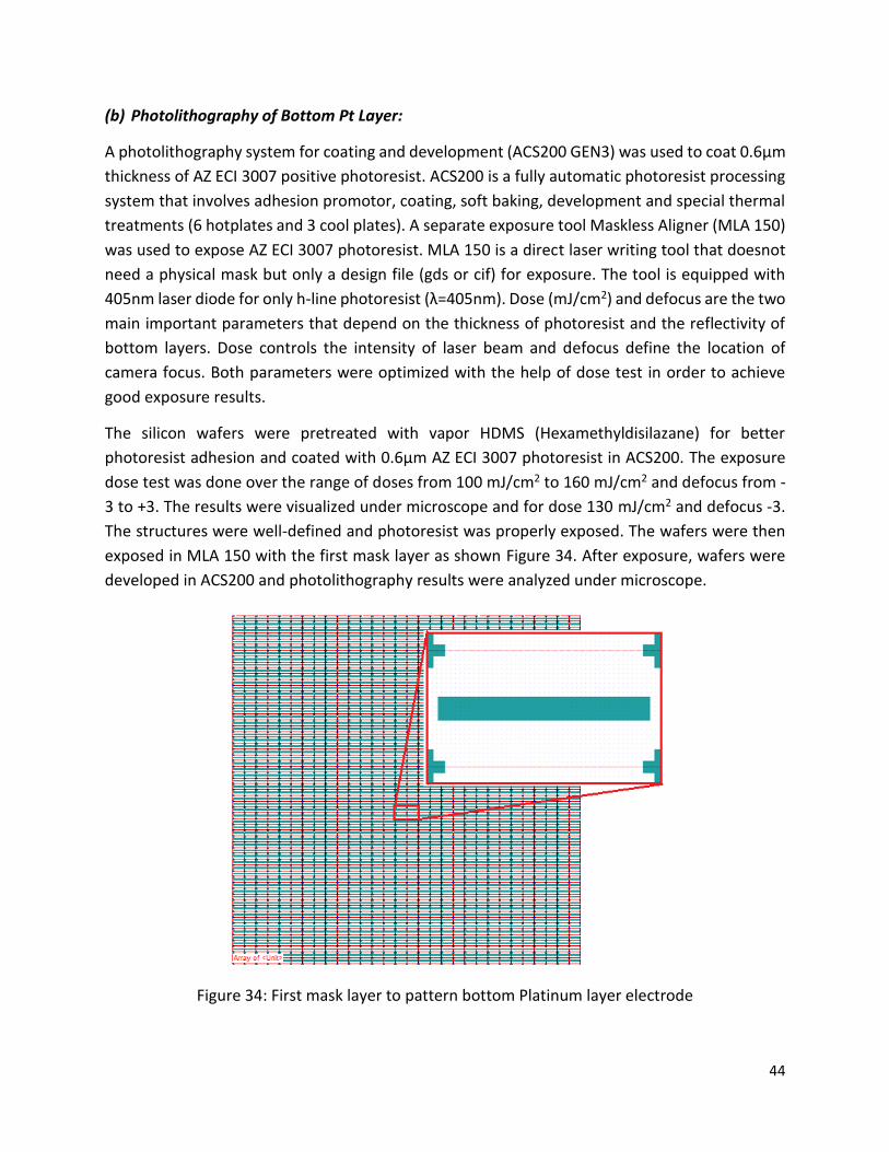
44
(b) Photolithography of Bottom Pt Layer:
A photolithography system for coating and development (ACS200 GEN3) was used to coat 0.6µm
thickness of AZ ECI 3007 positive photoresist. ACS200 is a fully automatic photoresist processing
system that involves adhesion promotor, coating, soft baking, development and special thermal
treatments (6 hotplates and 3 cool plates). A separate exposure tool Maskless Aligner (MLA 150)
was used to expose AZ ECI 3007 photoresist. MLA 150 is a direct laser writing tool that doesnot
need a physical mask but only a design file (gds or cif) for exposure. The tool is equipped with
405nm laser diode for only h-line photoresist (λ=405nm). Dose (mJ/cm2) and defocus are the two
main important parameters that depend on the thickness of photoresist and the reflectivity of
bottom layers. Dose controls the intensity of laser beam and defocus define the location of
camera focus. Both parameters were optimized with the help of dose test in order to achieve
good exposure results.
The silicon wafers were pretreated with vapor HDMS (Hexamethyldisilazane) for better
photoresist adhesion and coated with 0.6µm AZ ECI 3007 photoresist in ACS200. The exposure
dose test was done over the range of doses from 100 mJ/cm2 to 160 mJ/cm2 and defocus from -
3 to +3. The results were visualized under microscope and for dose 130 mJ/cm2 and defocus -3.
The structures were well-defined and photoresist was properly exposed. The wafers were then
exposed in MLA 150 with the first mask layer as shown Figure 34. After exposure, wafers were
developed in ACS200 and photolithography results were analyzed under microscope.
Figure 34: First mask layer to pattern bottom Platinum layer electrode
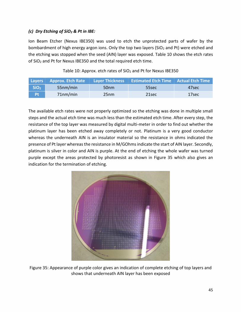
45
(c) Dry Etching of SiO2 & Pt in IBE:
Ion Beam Etcher (Nexus IBE350) was used to etch the unprotected parts of wafer by the
bombardment of high energy argon ions. Only the top two layers (SiO2 and Pt) were etched and
the etching was stopped when the seed (AIN) layer was exposed. Table 10 shows the etch rates
of SiO2 and Pt for Nexus IBE350 and the total required etch time.
Table 10: Approx. etch rates of SiO2 and Pt for Nexus IBE350
Layers Approx. Etch Rate Layer Thickness Estimated Etch Time Actual Etch Time
SiO2 55nm/min 50nm 55sec 47sec
Pt 71nm/min 25nm 21sec 17sec
The available etch rates were not properly optimized so the etching was done in multiple small
steps and the actual etch time was much less than the estimated etch time. After every step, the
resistance of the top layer was measured by digital multi-meter in order to find out whether the
platinum layer has been etched away completely or not. Platinum is a very good conductor
whereas the underneath AIN is an insulator material so the resistance in ohms indicated the
presence of Pt layer whereas the resistance in M/GOhms indicate the start of AIN layer. Secondly,
platinum is silver in color and AIN is purple. At the end of etching the whole wafer was turned
purple except the areas protected by photoresist as shown in Figure 35 which also gives an
indication for the termination of etching.
Figure 35: Appearance of purple color gives an indication of complete etching of top layers and shows that underneath AIN layer has been exposed
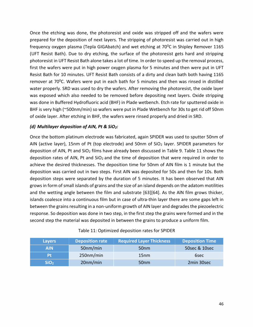
46
Once the etching was done, the photoresist and oxide was stripped off and the wafers were
prepared for the deposition of next layers. The stripping of photoresist was carried out in high
frequency oxygen plasma (Tepla GIGAbatch) and wet etching at 700C in Shipley Remover 1165
(UFT Resist Bath). Due to dry etching, the surface of the photoresist gets hard and stripping
photoresist in UFT Resist Bath alone takes a lot of time. In order to speed up the removal process,
first the wafers were put in high power oxygen plasma for 5 minutes and then were put in UFT
Resist Bath for 10 minutes. UFT Resist Bath consists of a dirty and clean bath both having 1165
remover at 700C. Wafers were put in each bath for 5 minutes and then was rinsed in distilled
water properly. SRD was used to dry the wafers. After removing the photoresist, the oxide layer
was exposed which also needed to be removed before depositing next layers. Oxide stripping
was done in Buffered Hydrofluoric acid (BHF) in Plade wetbench. Etch rate for sputtered oxide in
BHF is very high (~500nm/min) so wafers were put in Plade Wetbench for 30s to get rid off 50nm
of oxide layer. After etching in BHF, the wafers were rinsed properly and dried in SRD.
(d) Multilayer deposition of AIN, Pt & SiO2:
Once the bottom platinum electrode was fabricated, again SPIDER was used to sputter 50nm of
AIN (active layer), 15nm of Pt (top electrode) and 50nm of SiO2 layer. SPIDER parameters for
deposition of AIN, Pt and SiO2 films have already been discussed in Table 9. Table 11 shows the
deposition rates of AIN, Pt and SiO2 and the time of deposition that were required in order to
achieve the desired thicknesses. The deposition time for 50nm of AIN film is 1 minute but the
deposition was carried out in two steps. First AIN was deposited for 50s and then for 10s. Both
deposition steps were separated by the duration of 5 minutes. It has been observed that AIN
grows in form of small islands of grains and the size of an island depends on the adatom motilities
and the wetting angle between the film and substrate [63][64]. As the AlN film grows thicker,
islands coalesce into a continuous film but in case of ultra-thin layer there are some gaps left in
between the grains resulting in a non-uniform growth of AIN layer and degrades the piezoelectric
response. So deposition was done in two step, in the first step the grains were formed and in the
second step the material was deposited in between the grains to produce a uniform film.
Table 11: Optimized deposition rates for SPIDER
Layers Deposition rate Required Layer Thickness Deposition Time
AIN 50nm/min 50nm 50sec & 10sec
Pt 250nm/min 15nm 6sec
SiO2 20nm/min 50nm 2min 30sec
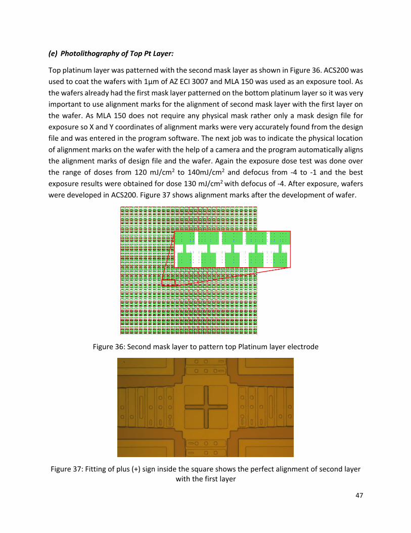
47
(e) Photolithography of Top Pt Layer:
Top platinum layer was patterned with the second mask layer as shown in Figure 36. ACS200 was
used to coat the wafers with 1µm of AZ ECI 3007 and MLA 150 was used as an exposure tool. As
the wafers already had the first mask layer patterned on the bottom platinum layer so it was very
important to use alignment marks for the alignment of second mask layer with the first layer on
the wafer. As MLA 150 does not require any physical mask rather only a mask design file for
exposure so X and Y coordinates of alignment marks were very accurately found from the design
file and was entered in the program software. The next job was to indicate the physical location
of alignment marks on the wafer with the help of a camera and the program automatically aligns
the alignment marks of design file and the wafer. Again the exposure dose test was done over
the range of doses from 120 mJ/cm2 to 140mJ/cm2 and defocus from -4 to -1 and the best
exposure results were obtained for dose 130 mJ/cm2 with defocus of -4. After exposure, wafers
were developed in ACS200. Figure 37 shows alignment marks after the development of wafer.
Figure 36: Second mask layer to pattern top Platinum layer electrode
Figure 37: Fitting of plus (+) sign inside the square shows the perfect alignment of second layer with the first layer

48
(f) Dry Etching of SiO2,Pt & AIN in STS:
Etching of SiO2, top Pt and AIN layers till the bottom Pt layer was the most difficult and critical
step of this process flow. The dry etching of SiO2, Pt and AIN was achieved by an inductively
coupled plasma system (STS Multiplex) using Cl2/Ar chemistry. STS Multiplex provides high
density and high ion current plasma at low pressure where argon ions bombard the target in
presence of chlorine gas. Table 12 shows the etch rates and etch time of SiO2, Pt and AIN for STS
Multiplex. It was essential to stop the etching when the bottom platinum layer was exposed. So
in order to achieve that the etching was done in multiple small steps and the resistance of top
layer was measured with digital multimeter in every step to get an idea regarding the material of
the top surface. End point system was also used to find out the current etching layer. End point
systems works with the intensity of light reflected from the surface of the wafer. Pt has high
reflectivity than AIN so light reflected by Pt surface has more intensity than AIN which was also
used as an indicator to find out the etching layer. The total time required to etch SiO2, Pt and AIN
layers was 2 minutes which was more than the time estimated from the etch rates. As the etching
was done in multiple steps, so for every step plasma needs some time to ramp up and reaches
its maximum intensity which overall takes longer than etching continuously. Once the etching
was done, the photoresist was stripped off and the wafers were ready for patterning of devices.
Table 12: Etch rates and etch time of SiO2, Pt and AIN for STS Multiplex
Layers Approx. Etch Rate Layer Thickness Estimated Etch Time
SiO2 70nm/min 50nm 42.8sec
Pt 27nm/min 15nm 33.3sec
AIN 285nm/min 50nm 10.4sec
(g) Photolithography of devices:
Third photolithographic step was done to pattern devices on the top Pt layer. All three wafers
were coated with 1µm of AZ ECI 3007 in ACS200 and were exposed in MLA 150. Exposure dose
test was not done for this stage because we already had the optimized MLA 150 exposure
parameters from the last photolithography stage. Figure 38 shows the third mask layer, which
consists of cantilevers and double clamped beam of variable dimensions. Again alignment marks
were used to align the third mask layer with the preceding layers on the wafer. Dose 130 mJ/cm2
and defocus -4 was used for exposure and ACS200 was used to develop the wafers.
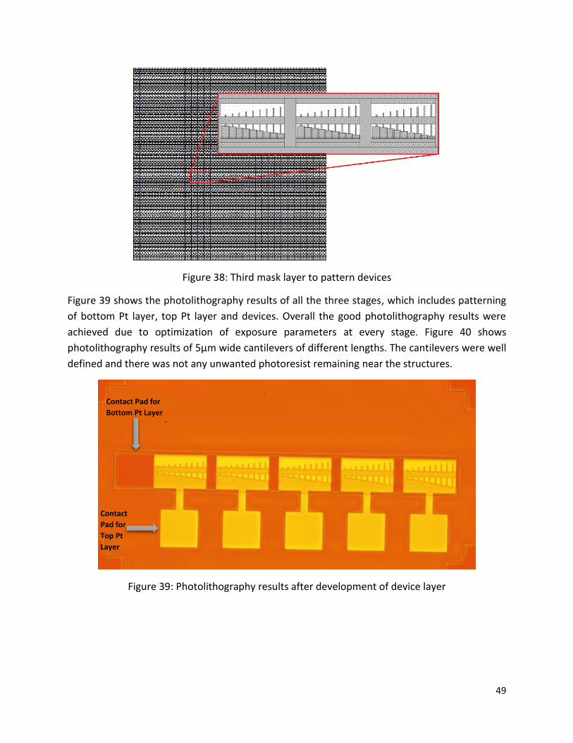
49
Figure 38: Third mask layer to pattern devices
Figure 39 shows the photolithography results of all the three stages, which includes patterning
of bottom Pt layer, top Pt layer and devices. Overall the good photolithography results were
achieved due to optimization of exposure parameters at every stage. Figure 40 shows
photolithography results of 5µm wide cantilevers of different lengths. The cantilevers were well
defined and there was not any unwanted photoresist remaining near the structures.
Figure 39: Photolithography results after development of device layer
Contact Pad for
Bottom Pt Layer
Contact
Pad for
Top Pt
Layer
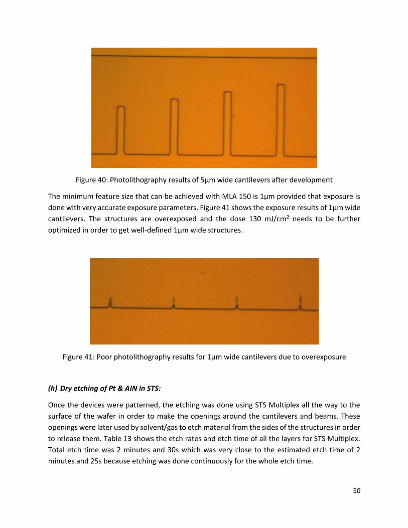
50
Figure 40: Photolithography results of 5µm wide cantilevers after development
The minimum feature size that can be achieved with MLA 150 is 1µm provided that exposure is
done with very accurate exposure parameters. Figure 41 shows the exposure results of 1µm wide
cantilevers. The structures are overexposed and the dose 130 mJ/cm2 needs to be further
optimized in order to get well-defined 1µm wide structures.
Figure 41: Poor photolithography results for 1µm wide cantilevers due to overexposure
(h) Dry etching of Pt & AIN in STS:
Once the devices were patterned, the etching was done using STS Multiplex all the way to the
surface of the wafer in order to make the openings around the cantilevers and beams. These
openings were later used by solvent/gas to etch material from the sides of the structures in order
to release them. Table 13 shows the etch rates and etch time of all the layers for STS Multiplex.
Total etch time was 2 minutes and 30s which was very close to the estimated etch time of 2
minutes and 25s because etching was done continuously for the whole etch time.
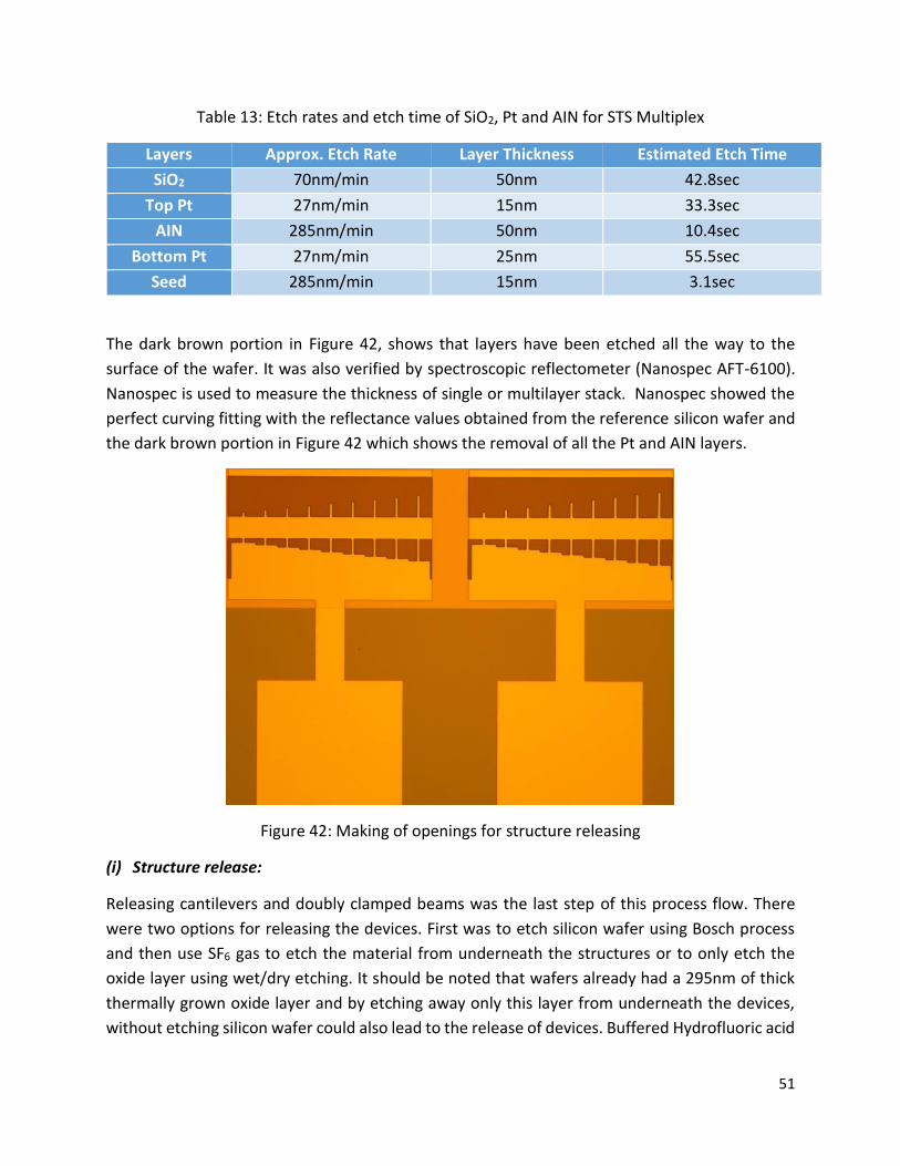
51
Table 13: Etch rates and etch time of SiO2, Pt and AIN for STS Multiplex
Layers Approx. Etch Rate Layer Thickness Estimated Etch Time
SiO2 70nm/min 50nm 42.8sec
Top Pt 27nm/min 15nm 33.3sec
AIN 285nm/min 50nm 10.4sec
Bottom Pt 27nm/min 25nm 55.5sec
Seed 285nm/min 15nm 3.1sec
The dark brown portion in Figure 42, shows that layers have been etched all the way to the
surface of the wafer. It was also verified by spectroscopic reflectometer (Nanospec AFT-6100).
Nanospec is used to measure the thickness of single or multilayer stack. Nanospec showed the
perfect curving fitting with the reflectance values obtained from the reference silicon wafer and
the dark brown portion in Figure 42 which shows the removal of all the Pt and AIN layers.
Figure 42: Making of openings for structure releasing
(i) Structure release:
Releasing cantilevers and doubly clamped beams was the last step of this process flow. There
were two options for releasing the devices. First was to etch silicon wafer using Bosch process
and then use SF6 gas to etch the material from underneath the structures or to only etch the
oxide layer using wet/dry etching. It should be noted that wafers already had a 295nm of thick
thermally grown oxide layer and by etching away only this layer from underneath the devices,
without etching silicon wafer could also lead to the release of devices. Buffered Hydrofluoric acid
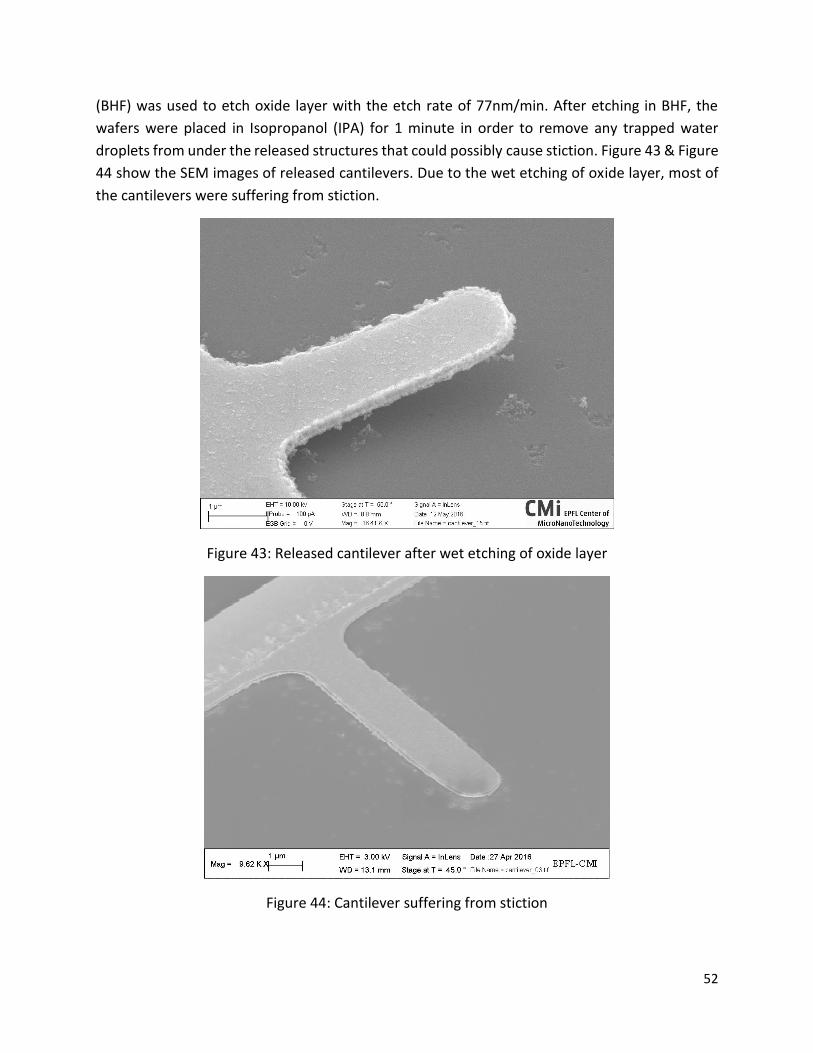
52
(BHF) was used to etch oxide layer with the etch rate of 77nm/min. After etching in BHF, the
wafers were placed in Isopropanol (IPA) for 1 minute in order to remove any trapped water
droplets from under the released structures that could possibly cause stiction. Figure 43 & Figure
44 show the SEM images of released cantilevers. Due to the wet etching of oxide layer, most of
the cantilevers were suffering from stiction.
Figure 43: Released cantilever after wet etching of oxide layer
Figure 44: Cantilever suffering from stiction
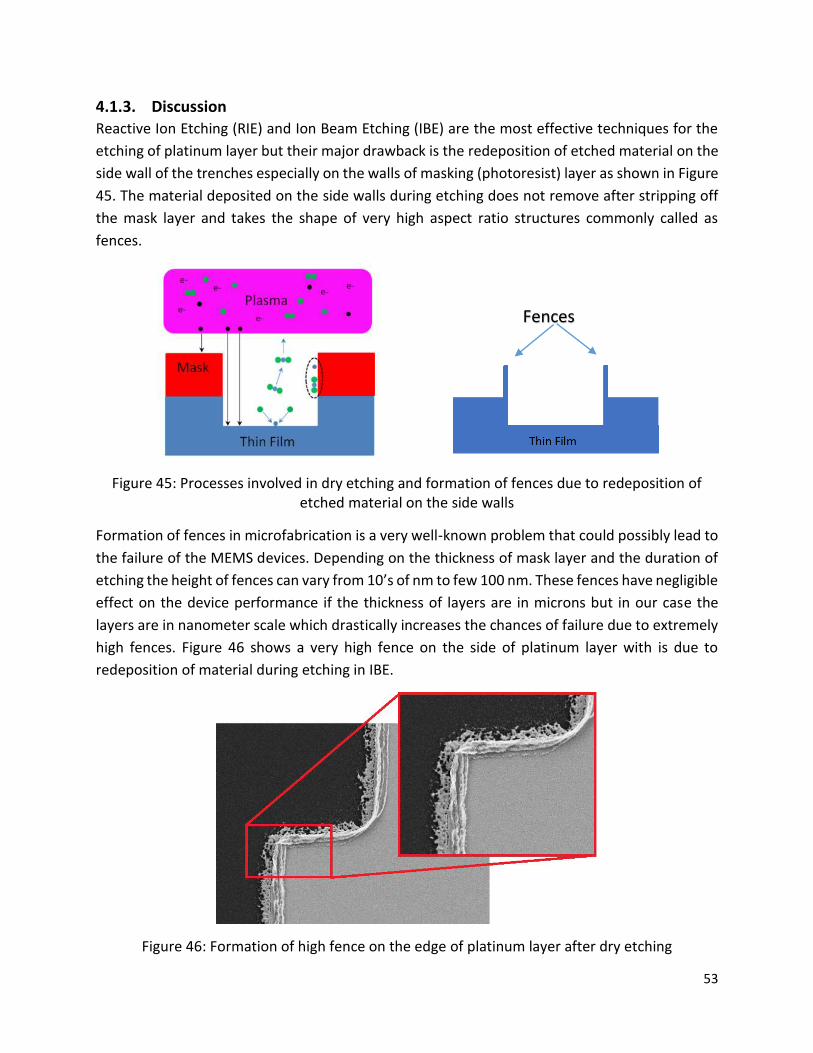
53
4.1.3. Discussion
Reactive Ion Etching (RIE) and Ion Beam Etching (IBE) are the most effective techniques for the
etching of platinum layer but their major drawback is the redeposition of etched material on the
side wall of the trenches especially on the walls of masking (photoresist) layer as shown in Figure
45. The material deposited on the side walls during etching does not remove after stripping off
the mask layer and takes the shape of very high aspect ratio structures commonly called as
fences.
Figure 45: Processes involved in dry etching and formation of fences due to redeposition of etched material on the side walls
Formation of fences in microfabrication is a very well-known problem that could possibly lead to
the failure of the MEMS devices. Depending on the thickness of mask layer and the duration of
etching the height of fences can vary from 10’s of nm to few 100 nm. These fences have negligible
effect on the device performance if the thickness of layers are in microns but in our case the
layers are in nanometer scale which drastically increases the chances of failure due to extremely
high fences. Figure 46 shows a very high fence on the side of platinum layer with is due to
redeposition of material during etching in IBE.
Figure 46: Formation of high fence on the edge of platinum layer after dry etching
Fences
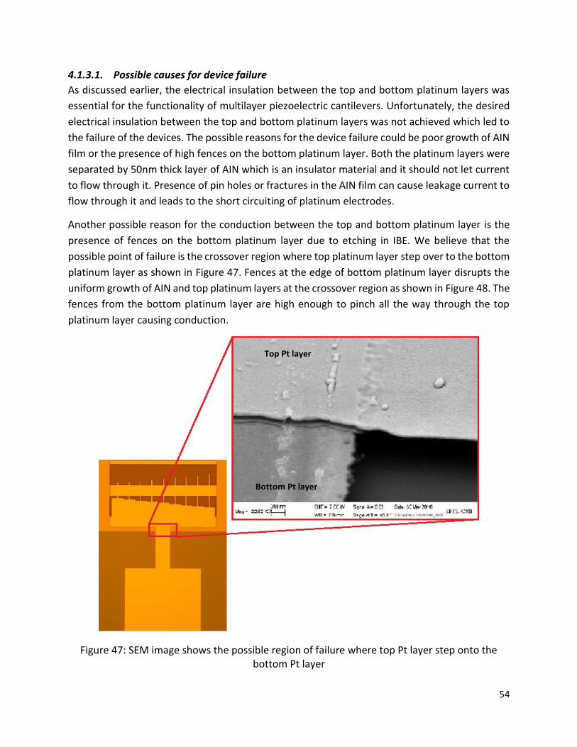
54
4.1.3.1. Possible causes for device failure
As discussed earlier, the electrical insulation between the top and bottom platinum layers was
essential for the functionality of multilayer piezoelectric cantilevers. Unfortunately, the desired
electrical insulation between the top and bottom platinum layers was not achieved which led to
the failure of the devices. The possible reasons for the device failure could be poor growth of AIN
film or the presence of high fences on the bottom platinum layer. Both the platinum layers were
separated by 50nm thick layer of AIN which is an insulator material and it should not let current
to flow through it. Presence of pin holes or fractures in the AIN film can cause leakage current to
flow through it and leads to the short circuiting of platinum electrodes.
Another possible reason for the conduction between the top and bottom platinum layer is the
presence of fences on the bottom platinum layer due to etching in IBE. We believe that the
possible point of failure is the crossover region where top platinum layer step over to the bottom
platinum layer as shown in Figure 47. Fences at the edge of bottom platinum layer disrupts the
uniform growth of AIN and top platinum layers at the crossover region as shown in Figure 48. The
fences from the bottom platinum layer are high enough to pinch all the way through the top
platinum layer causing conduction.
Figure 47: SEM image shows the possible region of failure where top Pt layer step onto the bottom Pt layer
Top Pt layer
Bottom Pt layer
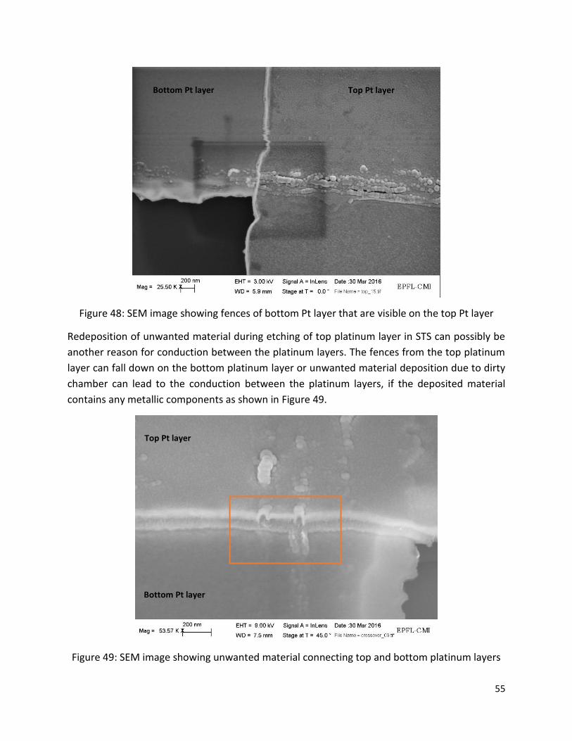
55
Figure 48: SEM image showing fences of bottom Pt layer that are visible on the top Pt layer
Redeposition of unwanted material during etching of top platinum layer in STS can possibly be
another reason for conduction between the platinum layers. The fences from the top platinum
layer can fall down on the bottom platinum layer or unwanted material deposition due to dirty
chamber can lead to the conduction between the platinum layers, if the deposited material
contains any metallic components as shown in Figure 49.
Figure 49: SEM image showing unwanted material connecting top and bottom platinum layers
Bottom Pt layer Top Pt layer
Top Pt layer
Bottom Pt layer
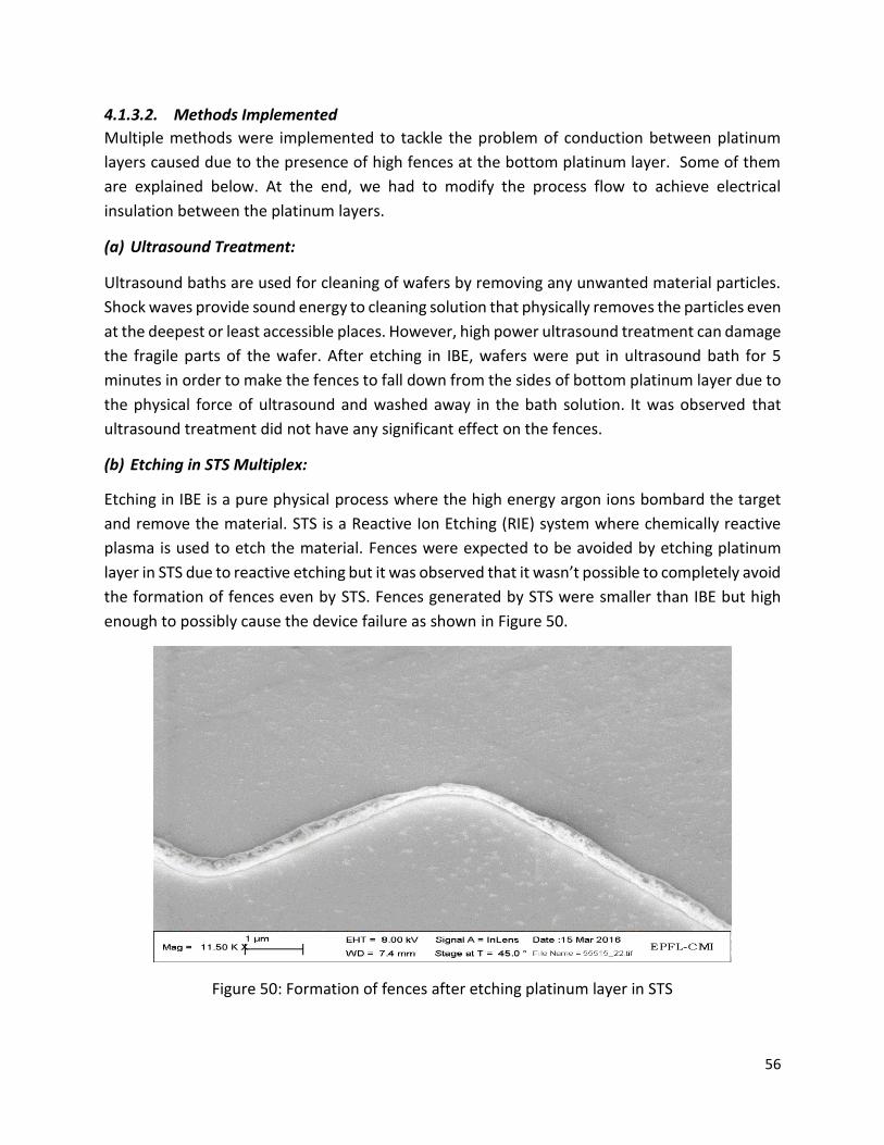
56
4.1.3.2. Methods Implemented
Multiple methods were implemented to tackle the problem of conduction between platinum
layers caused due to the presence of high fences at the bottom platinum layer. Some of them
are explained below. At the end, we had to modify the process flow to achieve electrical
insulation between the platinum layers.
(a) Ultrasound Treatment:
Ultrasound baths are used for cleaning of wafers by removing any unwanted material particles.
Shock waves provide sound energy to cleaning solution that physically removes the particles even
at the deepest or least accessible places. However, high power ultrasound treatment can damage
the fragile parts of the wafer. After etching in IBE, wafers were put in ultrasound bath for 5
minutes in order to make the fences to fall down from the sides of bottom platinum layer due to
the physical force of ultrasound and washed away in the bath solution. It was observed that
ultrasound treatment did not have any significant effect on the fences.
(b) Etching in STS Multiplex:
Etching in IBE is a pure physical process where the high energy argon ions bombard the target
and remove the material. STS is a Reactive Ion Etching (RIE) system where chemically reactive
plasma is used to etch the material. Fences were expected to be avoided by etching platinum
layer in STS due to reactive etching but it was observed that it wasn’t possible to completely avoid
the formation of fences even by STS. Fences generated by STS were smaller than IBE but high
enough to possibly cause the device failure as shown in Figure 50.
Figure 50: Formation of fences after etching platinum layer in STS
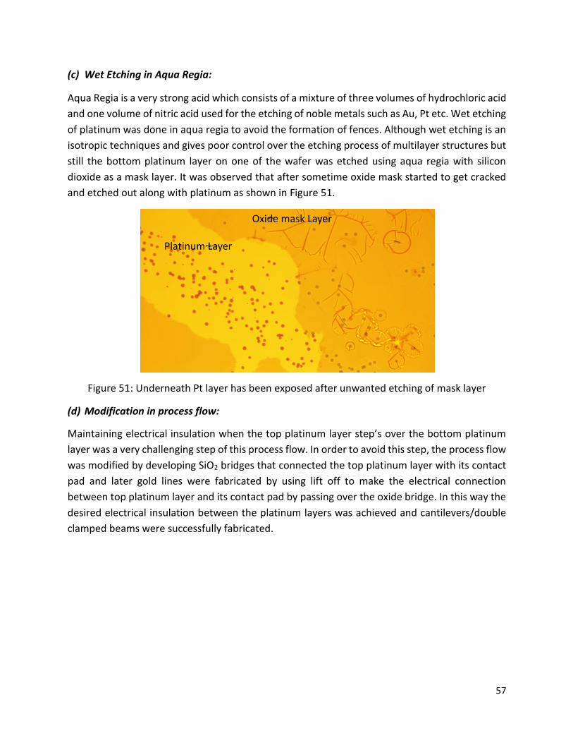
57
(c) Wet Etching in Aqua Regia:
Aqua Regia is a very strong acid which consists of a mixture of three volumes of hydrochloric acid
and one volume of nitric acid used for the etching of noble metals such as Au, Pt etc. Wet etching
of platinum was done in aqua regia to avoid the formation of fences. Although wet etching is an
isotropic techniques and gives poor control over the etching process of multilayer structures but
still the bottom platinum layer on one of the wafer was etched using aqua regia with silicon
dioxide as a mask layer. It was observed that after sometime oxide mask started to get cracked
and etched out along with platinum as shown in Figure 51.
Figure 51: Underneath Pt layer has been exposed after unwanted etching of mask layer
(d) Modification in process flow:
Maintaining electrical insulation when the top platinum layer step’s over the bottom platinum
layer was a very challenging step of this process flow. In order to avoid this step, the process flow
was modified by developing SiO2 bridges that connected the top platinum layer with its contact
pad and later gold lines were fabricated by using lift off to make the electrical connection
between top platinum layer and its contact pad by passing over the oxide bridge. In this way the
desired electrical insulation between the platinum layers was achieved and cantilevers/double
clamped beams were successfully fabricated.
Platinum Layer
Oxide mask Layer
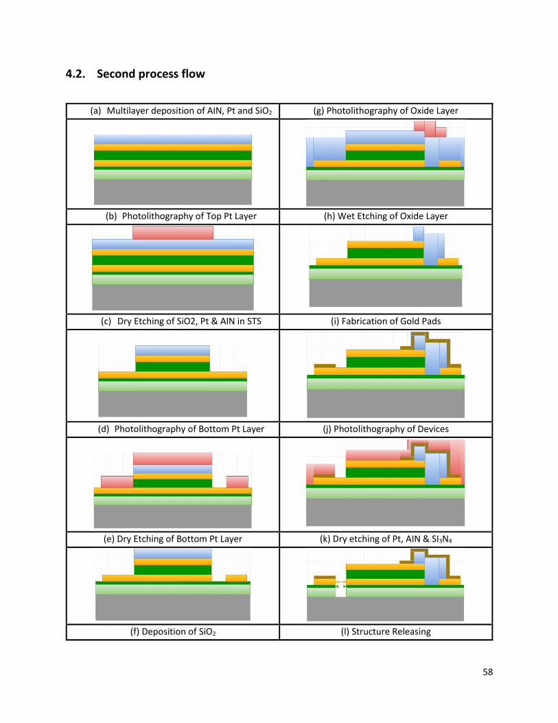
58
4.2. Second process flow
(a) Multilayer deposition of AIN, Pt and SiO2 (g) Photolithography of Oxide Layer
(b) Photolithography of Top Pt Layer (h) Wet Etching of Oxide Layer
(c) Dry Etching of SiO2, Pt & AIN in STS (i) Fabrication of Gold Pads
(d) Photolithography of Bottom Pt Layer (j) Photolithography of Devices
(e) Dry Etching of Bottom Pt Layer (k) Dry etching of Pt, AIN & SI3N4
(f) Deposition of SiO2 (l) Structure Releasing
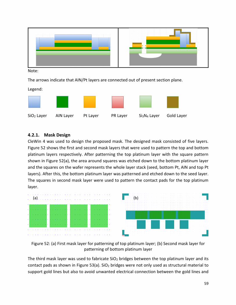
59
Note:
The arrows indicate that AIN/Pt layers are connected out of present section plane.
Legend:
SiO2 Layer AIN Layer Pt Layer PR Layer Si3N4 Layer Gold Layer
4.2.1. Mask Design
CleWin 4 was used to design the proposed mask. The designed mask consisted of five layers.
Figure 52 shows the first and second mask layers that were used to pattern the top and bottom
platinum layers respectively. After patterning the top platinum layer with the square pattern
shown in Figure 52(a), the area around squares was etched down to the bottom platinum layer
and the squares on the wafer represents the whole layer stack (seed, bottom Pt, AIN and top Pt
layers). After this, the bottom platinum layer was patterned and etched down to the seed layer.
The squares in second mask layer were used to pattern the contact pads for the top platinum
layer.
Figure 52: (a) First mask layer for patterning of top platinum layer; (b) Second mask layer for patterning of bottom platinum layer
The third mask layer was used to fabricate SiO2 bridges between the top platinum layer and its
contact pads as shown in Figure 53(a). SiO2 bridges were not only used as structural material to
support gold lines but also to avoid unwanted electrical connection between the gold lines and
(a) (b)

60
bottom platinum layer. Figure 53(b) shows the fourth mask layer that was used to make contact
pads for top and bottom platinum layers. As different top platinum squares are on the same
bottom platinum layer so only one contact pad on bottom platinum layer was enough to provide
potential to all the devices whereas different squares had their separate contact pads for
providing potential to top platinum layer.
Figure 53: (a) Third mask layer for patterning of SiO2 bridges; (b) Fourth mask layer for patterning of contact pads
The fifth mask layer was the device layer which consisted of cantilevers and clamp-clamp beams
of different dimensions as shown in Figure 54. The dimensions of the devices ranges from 2x1µm
to 50x5µm. The devices were patterned only on the four layers stack squares and were etched
down all the way till the surface of the wafer in order to make the openings which were later
used for releasing the devices.
Figure 54: Fifth mask layer for patterning of devices on top platinum layer
4.2.2. Experimental work
(a) Multilayer deposition of AIN, Pt and SiO2:
Three 4’’ wafers (63673, 63674 & 63675) were used for the fabrication of this process flow. These
wafer were already coated with 50nm of high stress silicon nitride layer in order to minimize the
overall compressive stress in the structure. The wafers were coated with the whole layer stack
(b) (a)
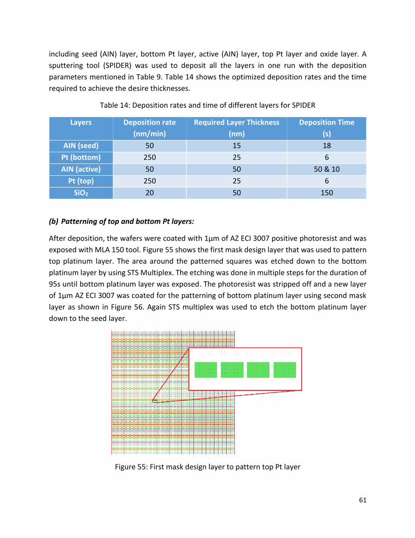
61
including seed (AIN) layer, bottom Pt layer, active (AIN) layer, top Pt layer and oxide layer. A
sputtering tool (SPIDER) was used to deposit all the layers in one run with the deposition
parameters mentioned in Table 9. Table 14 shows the optimized deposition rates and the time
required to achieve the desire thicknesses.
Table 14: Deposition rates and time of different layers for SPIDER
Layers Deposition rate
(nm/min)
Required Layer Thickness
(nm)
Deposition Time
(s)
AIN (seed) 50 15 18
Pt (bottom) 250 25 6
AIN (active) 50 50 50 & 10
Pt (top) 250 25 6
SiO2 20 50 150
(b) Patterning of top and bottom Pt layers:
After deposition, the wafers were coated with 1µm of AZ ECI 3007 positive photoresist and was
exposed with MLA 150 tool. Figure 55 shows the first mask design layer that was used to pattern
top platinum layer. The area around the patterned squares was etched down to the bottom
platinum layer by using STS Multiplex. The etching was done in multiple steps for the duration of
95s until bottom platinum layer was exposed. The photoresist was stripped off and a new layer
of 1µm AZ ECI 3007 was coated for the patterning of bottom platinum layer using second mask
layer as shown in Figure 56. Again STS multiplex was used to etch the bottom platinum layer
down to the seed layer.
Figure 55: First mask design layer to pattern top Pt layer

62
Figure 56: Second mask layer for patterning of bottom Pt layer
(c) Fabrication of SiO2 bridges:
Fabrication of SiO2 bridges was the most critical step of this process flow. The purpose of SiO2
bridges was to make a path between the top platinum layer and its contact pads. 100nm of SiO2
layer was deposited by SPIDER and pattered by MLA 150. Figure 57 shows the third mask layer,
which was used to pattern oxide layer. Buffered hydrofluoric acid (BHF) was used to etch the
unprotected areas of oxide layer and at the end of etching, 65x60µm dimension of oxide patches
were left in between the top platinum layer and its contact pads as shown in Figure 58. Later gold
lines were fabricated to make an electrical connection between the top platinum layer and its
contact pads.
Figure 57: Third mask layer for patterning of SiO2 bridges

63
Figure 58: Fabrication of SiO2 bridges for electrical insulation between different layers
The purpose of SiO2 bridges was to act not only as a structural support to hold the gold lines but
also to provide complete electrical insulation between the gold lines and bottom platinum layer.
In Figure 58, SiO2 bridges are passing over the bottom platinum layer and then connecting with
the top platinum layer. If the bridges get broken at the crossover point, then there is a very high
probability that gold line will get in contact with the bottom platinum layer and will cause short
circuiting of top and bottom platinum layers. So it is essential to have well defined and uniform
oxide bridges. Figure 59 shows few examples of poor oxide bridges due to over etching of SiO2
layer in BHF solution. Broken bridges can be seen from the sides which could possibly leads to
the conduction between top and bottom platinum layers.
Figure 59: Broken SiO2 bridges due to over etching of SiO2 layer in BHF
Top Pt Layer
Contact Pad
for top Pt
layer
Bottom Pt Layer
Top Pt Layer
Contact Pad for
top Pt layer
SiO2 Bridge
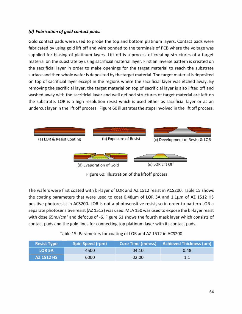
64
(d) Fabrication of gold contact pads:
Gold contact pads were used to probe the top and bottom platinum layers. Contact pads were
fabricated by using gold lift off and wire bonded to the terminals of PCB where the voltage was
supplied for biasing of platinum layers. Lift off is a process of creating structures of a target
material on the substrate by using sacrificial material layer. First an inverse pattern is created on
the sacrificial layer in order to make openings for the target material to reach the substrate
surface and then whole wafer is deposited by the target material. The target material is deposited
on top of sacrificial layer except in the regions where the sacrificial layer was etched away. By
removing the sacrificial layer, the target material on top of sacrificial layer is also lifted off and
washed away with the sacrificial layer and well defined structures of target material are left on
the substrate. LOR is a high resolution resist which is used either as sacrificial layer or as an
undercut layer in the lift off process. Figure 60 illustrates the steps involved in the lift off process.
The wafers were first coated with bi-layer of LOR and AZ 1512 resist in ACS200. Table 15 shows
the coating parameters that were used to coat 0.48µm of LOR 5A and 1.1µm of AZ 1512 HS
positive photoresist in ACS200. LOR is not a photosensitive resist, so in order to pattern LOR a
separate photosensitive resist (AZ 1512) was used. MLA 150 was used to expose the bi-layer resist
with dose 65mJ/cm2 and defocus of -6. Figure 61 shows the fourth mask layer which consists of
contact pads and the gold lines for connecting top platinum layer with its contact pads.
Table 15: Parameters for coating of LOR and AZ 1512 in ACS200
Resist Type Spin Speed (rpm) Cure Time (mm:ss) Achieved Thickness (um)
LOR 5A 4500 04:10 0.48
AZ 1512 HS 6000 02:00 1.1
(a) LOR & Resist Coating (b) Exposure of Resist (c) Development of Resist & LOR
(d) Evaporation of Gold (e) LOR Lift Off
Figure 60: Illustration of the liftoff process

65
Figure 61: Fourth mask layer for patterning of gold contact pads
Development of photosensitive resist makes an opening for the etching solution to attack LOR
and etch it away. Undercuts in LOR layer was observed due to isotropic etching. AZ 426 MIF
solution was used for the development of both the resist layers. After development, baking was
done at 100 0C for 2 minutes to improve the stability of photoresist. Figure 62 shows the
photolithography results where contact pads have desired openings in the LOR layer for gold
deposition.
Figure 62: Photolithography of contact pads for gold deposition
100nm of gold layer was deposited on the wafers by using an evaporation tool (Leybold Optics
Lab 600H). Lab 600H uses e-beam evaporation where electron beam is used to evaporate the
metal. A high energy electron beam is directed towards the crucible containing gold. The kinetic
energy of the electrons is converted into heat upon impact to evaporate gold. Distance between
the source and target is very important for liftoff process. The distance of 1.010m was maintained
between the source and target in order to maintain angle at 900 between the wafers and the
incident flux. Figure 63 shows the surface of wafer after gold deposition.
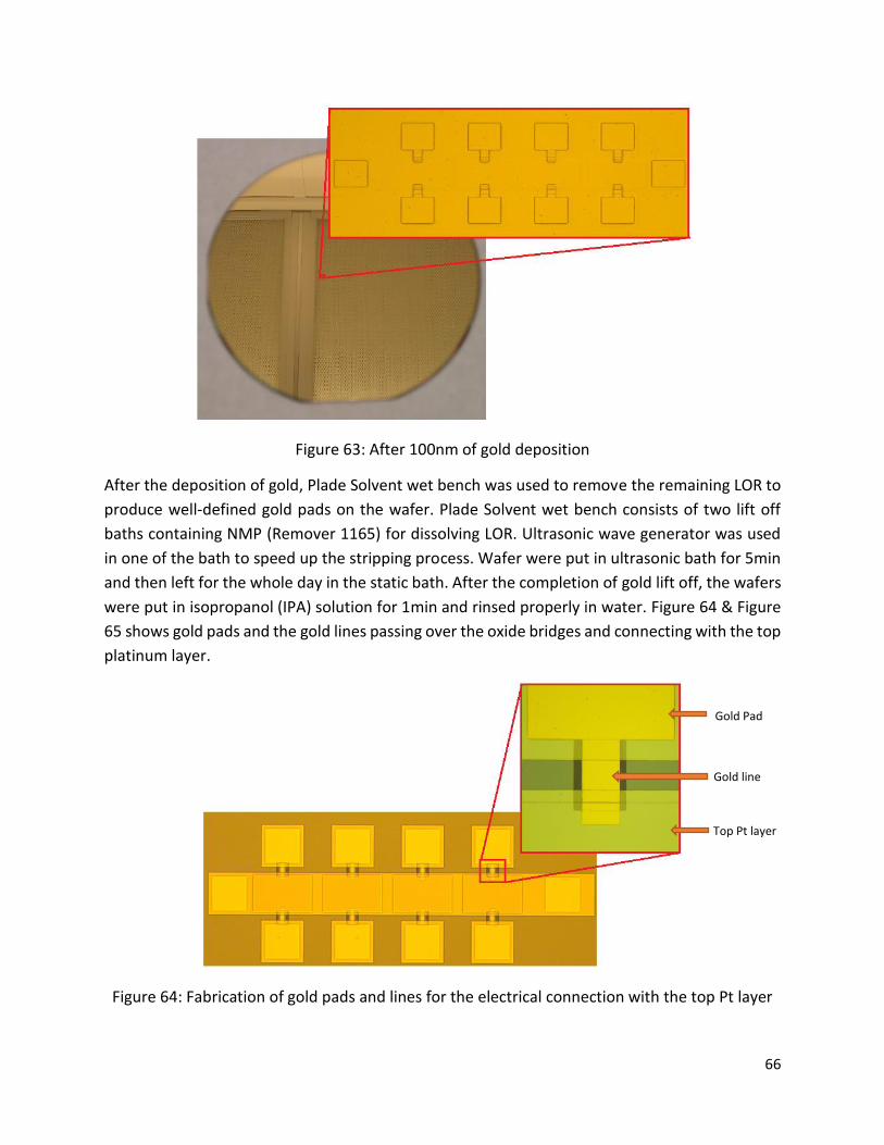
66
Figure 63: After 100nm of gold deposition
After the deposition of gold, Plade Solvent wet bench was used to remove the remaining LOR to
produce well-defined gold pads on the wafer. Plade Solvent wet bench consists of two lift off
baths containing NMP (Remover 1165) for dissolving LOR. Ultrasonic wave generator was used
in one of the bath to speed up the stripping process. Wafer were put in ultrasonic bath for 5min
and then left for the whole day in the static bath. After the completion of gold lift off, the wafers
were put in isopropanol (IPA) solution for 1min and rinsed properly in water. Figure 64 & Figure
65 shows gold pads and the gold lines passing over the oxide bridges and connecting with the top
platinum layer.
Figure 64: Fabrication of gold pads and lines for the electrical connection with the top Pt layer
Gold Pad
Gold line
Top Pt layer
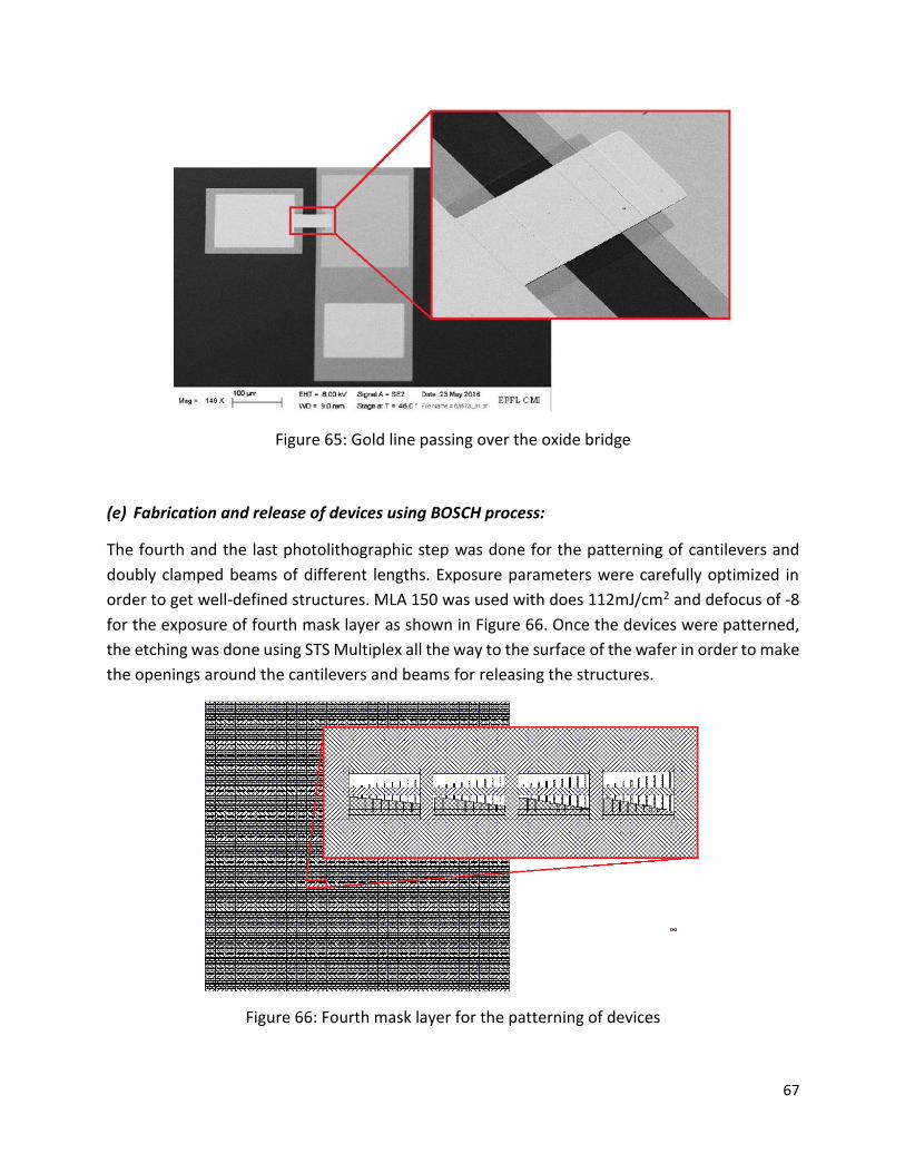
67
Figure 65: Gold line passing over the oxide bridge
(e) Fabrication and release of devices using BOSCH process:
The fourth and the last photolithographic step was done for the patterning of cantilevers and
doubly clamped beams of different lengths. Exposure parameters were carefully optimized in
order to get well-defined structures. MLA 150 was used with does 112mJ/cm2 and defocus of -8
for the exposure of fourth mask layer as shown in Figure 66. Once the devices were patterned,
the etching was done using STS Multiplex all the way to the surface of the wafer in order to make
the openings around the cantilevers and beams for releasing the structures.
Figure 66: Fourth mask layer for the patterning of devices
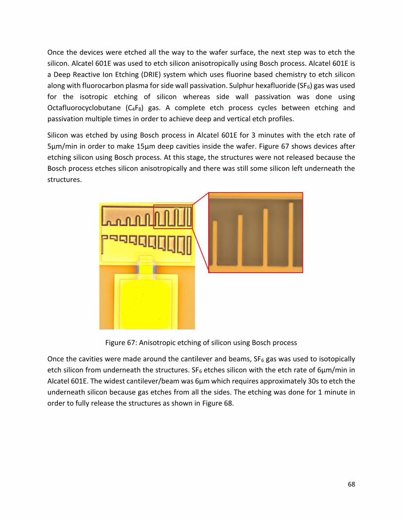
68
Once the devices were etched all the way to the wafer surface, the next step was to etch the
silicon. Alcatel 601E was used to etch silicon anisotropically using Bosch process. Alcatel 601E is
a Deep Reactive Ion Etching (DRIE) system which uses fluorine based chemistry to etch silicon
along with fluorocarbon plasma for side wall passivation. Sulphur hexafluoride (SF6) gas was used
for the isotropic etching of silicon whereas side wall passivation was done using
Octafluorocyclobutane (C4F8) gas. A complete etch process cycles between etching and
passivation multiple times in order to achieve deep and vertical etch profiles.
Silicon was etched by using Bosch process in Alcatel 601E for 3 minutes with the etch rate of
5µm/min in order to make 15µm deep cavities inside the wafer. Figure 67 shows devices after
etching silicon using Bosch process. At this stage, the structures were not released because the
Bosch process etches silicon anisotropically and there was still some silicon left underneath the
structures.
Figure 67: Anisotropic etching of silicon using Bosch process
Once the cavities were made around the cantilever and beams, SF6 gas was used to isotopically
etch silicon from underneath the structures. SF6 etches silicon with the etch rate of 6µm/min in
Alcatel 601E. The widest cantilever/beam was 6µm which requires approximately 30s to etch the
underneath silicon because gas etches from all the sides. The etching was done for 1 minute in
order to fully release the structures as shown in Figure 68.

69
Figure 68: Cantilever tips are out of focus due to bending downwards
Figure 69 & Figure 70 shows SEM images of the cantilevers and double clamped beams. The
structures are completely released and the cavity is deep enough to refrain cantilever tips from
touching the ground.
Figure 69: SEM image showing etched cavity and released cantilevers and doubly clamped beams
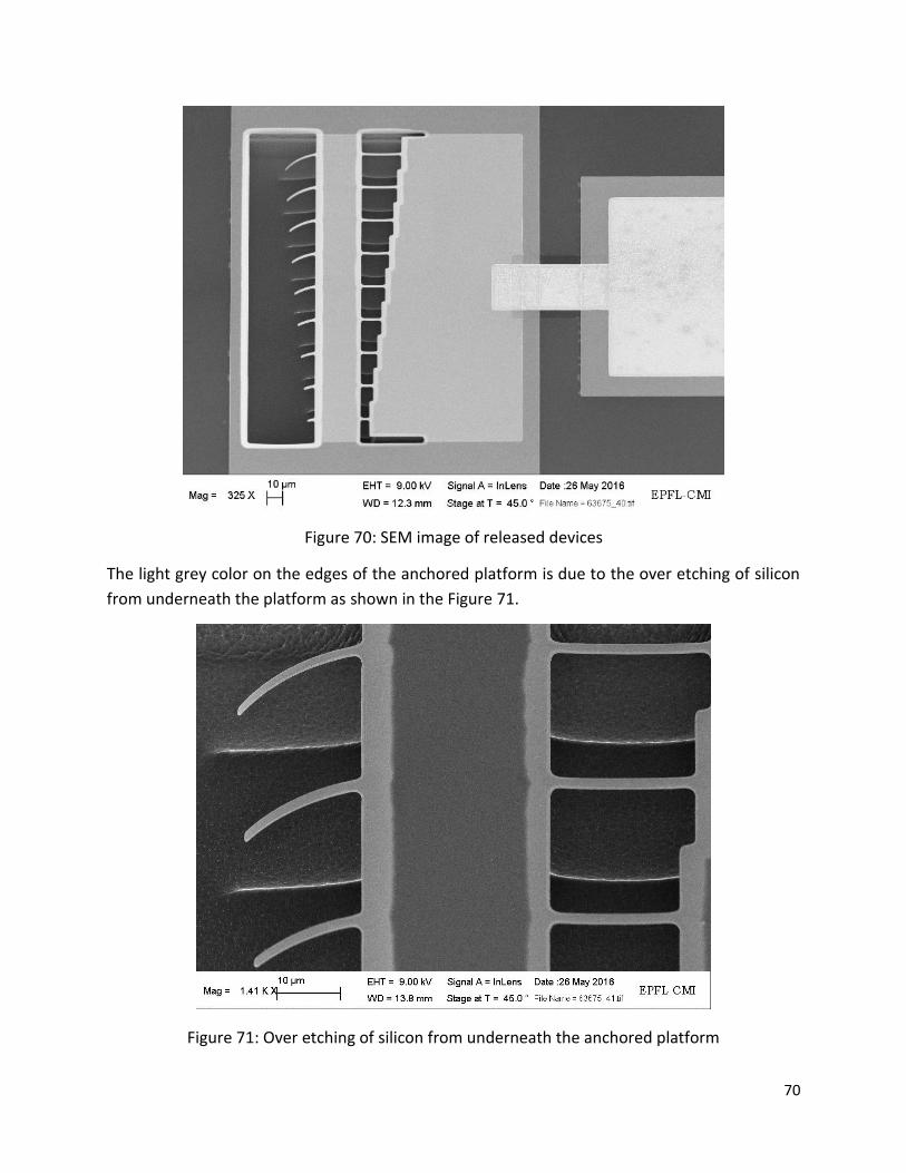
70
Figure 70: SEM image of released devices
The light grey color on the edges of the anchored platform is due to the over etching of silicon
from underneath the platform as shown in the Figure 71.
Figure 71: Over etching of silicon from underneath the anchored platform
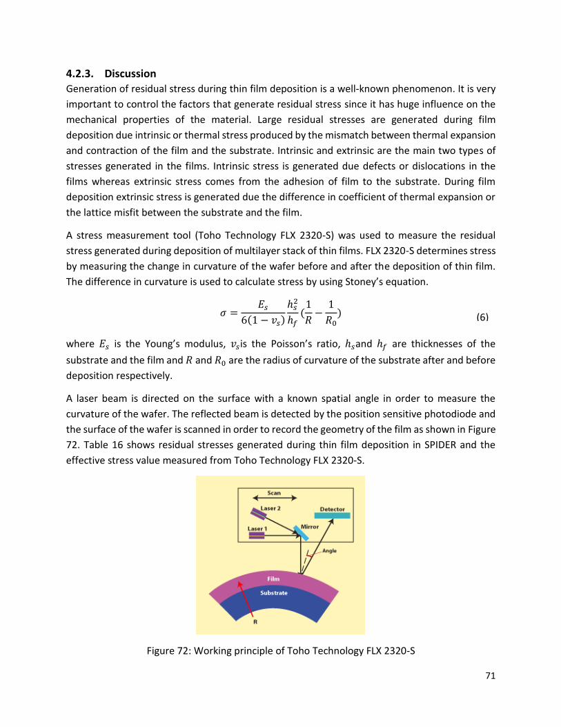
71
4.2.3. Discussion
Generation of residual stress during thin film deposition is a well-known phenomenon. It is very
important to control the factors that generate residual stress since it has huge influence on the
mechanical properties of the material. Large residual stresses are generated during film
deposition due intrinsic or thermal stress produced by the mismatch between thermal expansion
and contraction of the film and the substrate. Intrinsic and extrinsic are the main two types of
stresses generated in the films. Intrinsic stress is generated due defects or dislocations in the
films whereas extrinsic stress comes from the adhesion of film to the substrate. During film
deposition extrinsic stress is generated due the difference in coefficient of thermal expansion or
the lattice misfit between the substrate and the film.
A stress measurement tool (Toho Technology FLX 2320-S) was used to measure the residual
stress generated during deposition of multilayer stack of thin films. FLX 2320-S determines stress
by measuring the change in curvature of the wafer before and after the deposition of thin film.
The difference in curvature is used to calculate stress by using Stoney’s equation.
𝜎 =𝐸𝑠
6(1 − 𝑣𝑠)
ℎ𝑠2
ℎ𝑓(
1
𝑅−
1
𝑅0)
where 𝐸𝑠 is the Young’s modulus, 𝑣𝑠is the Poisson’s ratio, ℎ𝑠and ℎ𝑓 are thicknesses of the
substrate and the film and 𝑅 and 𝑅0 are the radius of curvature of the substrate after and before
deposition respectively.
A laser beam is directed on the surface with a known spatial angle in order to measure the
curvature of the wafer. The reflected beam is detected by the position sensitive photodiode and
the surface of the wafer is scanned in order to record the geometry of the film as shown in Figure
72. Table 16 shows residual stresses generated during thin film deposition in SPIDER and the
effective stress value measured from Toho Technology FLX 2320-S.
Figure 72: Working principle of Toho Technology FLX 2320-S
(6)
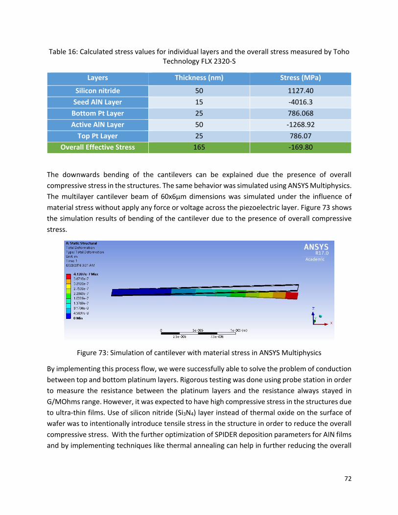
72
Table 16: Calculated stress values for individual layers and the overall stress measured by Toho Technology FLX 2320-S
Layers Thickness (nm) Stress (MPa)
Silicon nitride 50 1127.40
Seed AlN Layer 15 -4016.3
Bottom Pt Layer 25 786.068
Active AlN Layer 50 -1268.92
Top Pt Layer 25 786.07
Overall Effective Stress 165 -169.80
The downwards bending of the cantilevers can be explained due the presence of overall
compressive stress in the structures. The same behavior was simulated using ANSYS Multiphysics.
The multilayer cantilever beam of 60x6µm dimensions was simulated under the influence of
material stress without apply any force or voltage across the piezoelectric layer. Figure 73 shows
the simulation results of bending of the cantilever due to the presence of overall compressive
stress.
Figure 73: Simulation of cantilever with material stress in ANSYS Multiphysics
By implementing this process flow, we were successfully able to solve the problem of conduction
between top and bottom platinum layers. Rigorous testing was done using probe station in order
to measure the resistance between the platinum layers and the resistance always stayed in
G/MOhms range. However, it was expected to have high compressive stress in the structures due
to ultra-thin films. Use of silicon nitride (Si3N4) layer instead of thermal oxide on the surface of
wafer was to intentionally introduce tensile stress in the structure in order to reduce the overall
compressive stress. With the further optimization of SPIDER deposition parameters for AIN films
and by implementing techniques like thermal annealing can help in further reducing the overall
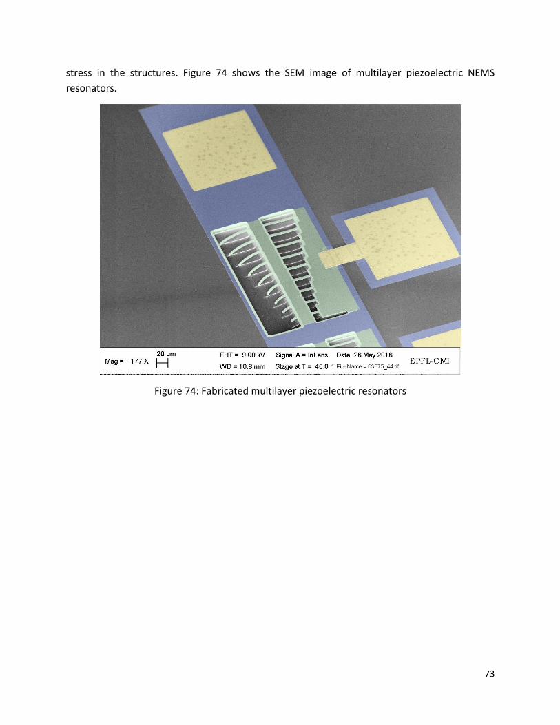
73
stress in the structures. Figure 74 shows the SEM image of multilayer piezoelectric NEMS
resonators.
Figure 74: Fabricated multilayer piezoelectric resonators
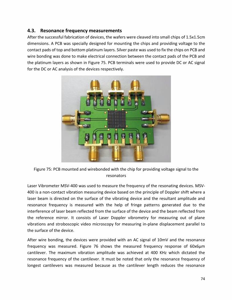
74
4.3. Resonance frequency measurements After the successful fabrication of devices, the wafers were cleaved into small chips of 1.5x1.5cm
dimensions. A PCB was specially designed for mounting the chips and providing voltage to the
contact pads of top and bottom platinum layers. Silver paste was used to fix the chips on PCB and
wire bonding was done to make electrical connection between the contact pads of the PCB and
the platinum layers as shown in Figure 75. PCB terminals were used to provide DC or AC signal
for the DC or AC analysis of the devices respectively.
Figure 75: PCB mounted and wirebonded with the chip for providing voltage signal to the
resonators
Laser Vibrometer MSV-400 was used to measure the frequency of the resonating devices. MSV-
400 is a non-contact vibration measuring device based on the principle of Doppler shift where a
laser beam is directed on the surface of the vibrating device and the resultant amplitude and
resonance frequency is measured with the help of fringe patterns generated due to the
interference of laser beam reflected from the surface of the device and the beam reflected from
the reference mirror. It consists of Laser Doppler vibrometry for measuring out of plane
vibrations and stroboscopic video microscopy for measuring in-plane displacement parallel to
the surface of the device.
After wire bonding, the devices were provided with an AC signal of 10mV and the resonance
frequency was measured. Figure 76 shows the measured frequency response of 60x6µm
cantilever. The maximum vibration amplitude was achieved at 400 KHz which dictated the
resonance frequency of the cantilever. It must be noted that only the resonance frequency of
longest cantilevers was measured because as the cantilever length reduces the resonance

75
frequency increases and in our case most of the cantilevers had resonance frequencies shifted in
MHz range and MSV-400 cannot measure vibrations higher than 1 MHz.
Figure 76: Resonance frequency of 60µm long cantilever measured with Laser Vibrometer MSV-
400
As mentioned in the chapter 3, the generation of stress due to applied voltage shifts the
resonance frequency of the beam. Similarly, the presence of material stress also has a significant
effect on the natural frequency of the beam. It is believed that the huge difference in the
measured and the simulated resonance frequency of 60µm long cantilever is due to the presence
of high compressive material stress in the structures and there is also a possibility that the
cantilever tip was touching the ground during frequency measurements.
0
0.01
0.02
0.03
0.04
0.05
0.06
3.8E+05 3.8E+05 3.9E+05 3.9E+05 4.0E+05 4.0E+05 4.1E+05 4.1E+05 4.2E+05 4.2E+05 4.3E+05
Ou
tpu
t Si
gnal
(V
)
Frequency (Hz)
Resonance Frequency for 60x6µm Cantilever
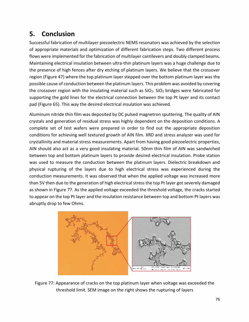
76
5. Conclusion Successful fabrication of multilayer piezoelectric NEMS resonators was achieved by the selection
of appropriate materials and optimization of different fabrication steps. Two different process
flows were implemented for the fabrication of multilayer cantilevers and doubly clamped beams.
Maintaining electrical insulation between ultra-thin platinum layers was a huge challenge due to
the presence of high fences after dry etching of platinum layers. We believe that the crossover
region (Figure 47) where the top platinum layer stepped over the bottom platinum layer was the
possible cause of conduction between the platinum layers. This problem was avoided by covering
the crossover region with the insulating material such as SiO2. SiO2 bridges were fabricated for
supporting the gold lines for the electrical connection between the top Pt layer and its contact
pad (Figure 65). This way the desired electrical insulation was achieved.
Aluminum nitride thin film was deposited by DC pulsed magnetron sputtering. The quality of AIN
crystals and generation of residual stress was highly dependent on the deposition conditions. A
complete set of test wafers were prepared in order to find out the appropriate deposition
conditions for achieving well textured growth of AIN film. XRD and stress analyzer was used for
crystallinity and material stress measurements. Apart from having good piezoelectric properties,
AIN should also act as a very good insulating material. 50nm thin film of AIN was sandwiched
between top and bottom platinum layers to provide desired electrical insulation. Probe station
was used to measure the conduction between the platinum layers. Dielectric breakdown and
physical rupturing of the layers due to high electrical stress was experienced during the
conduction measurements. It was observed that when the applied voltage was increased more
than 5V then due to the generation of high electrical stress the top Pt layer got severely damaged
as shown in Figure 77. As the applied voltage exceeded the threshold voltage, the cracks started
to appear on the top Pt layer and the insulation resistance between top and bottom Pt layers was
abruptly drop to few Ohms.
Figure 77: Appearance of cracks on the top platinum layer when voltage was exceeded the
threshold limit. SEM image on the right shows the rupturing of layers

77
Presence of high compressive stress in the AIN layer was responsible for the downwards bending
of the cantilever beams. The variation in the resonance frequency of simulated and measured
values for 60µm long cantilever beam was due to the touching of cantilever tip with the surface
of the wafer during resonance frequency measurements. In future, we further need to optimize
the deposition parameters for AIN thin film and implement techniques like thermal annealing in
order to reduce the overall residual stress in the structures.
78
6. References [1] J. Ma, “Advanced MEMS-based technologies and displays,” vol. 37, pp. 2–10, 2015.
[2] J. Wang and X. Qian, “Application and Development of MEMS in the Field of Aerospace,” vol. 643, pp. 72–76, 2014.
[3] P. F. Partnership, “Prime Faraday Technology Watch An Introduction to MEMS ( Micro-electromechanical Systems ),” no. January. 2002.
[4] G. Villanueva, J. Bausells, and J. Brugger, “Grand challenge in N/ MEMS,” vol. 1, no. January, 2016.
[5] X. F. Zha, “MEMS/NEMS Handbook Techniques and Applications,” C. T. Leondes, Ed. pp. 2–32.
[6] R. P. Feynman, “Plenty of Room at the Bottom,” no. December, 1959.
[7] Nanotechweb review, “Quantum-dot TVs seed a bright future,” 2015.
[8] S. Schmid, L. G. Villanueva, and M. L. Roukes, Fundamentals of Nanomechanical Resonators. 2016.
[9] T. Ono, X. Li, H. Miyashita, M. Esashi, T. Ono, X. Li, and H. Miyashita, “Mass sensing of adsorbed molecules in sub-picogram sample with ultrathin silicon resonator,” vol. 1240, no. May, 2016.
[10] L. Nicu, V. Auzelyte, L. G. Villanueva, N. Barniol, and F. Perez-murano, “Chapter 9: Nanoelectromechanical Systems ( NEMS ),” in Resonant MEMS–Fundamentals, Implementation and Application, 1st ed., O. Brand, I. Dufour, S. M. Heinrich, and F. Josse, Eds. Wiley-VCH Verlag GmbH & Co. KGaA, 2015, pp. 203–231.
[11] O. Brand and H. Baltes, “Micromachined Resonant Sensors - an Overview.” pp. 4–14.
[12] S. K. Vashist, “A Review of Microcantilevers for Sensing Applications,” AZoNano, 2007.
[13] J. Lu, T. Ikehara, Y. Zhang, T. Mihara, T. Itoh, and R. Maeda, “High Quality Factor Silicon Cantilever Driven by PZT Actuator for Resonant Based Mass Detection,” no. April, pp. 1–6, 2008.
[14] K. Jensen, K. Kim, and A. Zettl, “An atomic-resolution nanomechanical mass sensor,” Nat. Nanotechnol., vol. 3, no. 9, pp. 533–7, 2008.
[15] J. Fritz, “Cantilever biosensors,” no. i, pp. 855–863, 2008.
[16] S. Schmid, L. G. Villanueva, and M. L. Roukes, “Chapter 2: Quality Factor,” in Fundamentals of Nanomechanical Resonators, Springer International Publishing Switzerland 2016, 2016, pp. 57–90.
[17] M. Nordström, S. Keller, M. Lillemose, A. Johansson, S. Dohn, D. Haefliger, G. Blagoi, M. Havsteen-jakobsen, and A. Boisen, “SU-8 Cantilevers for Bio/chemical Sensing; Fabrication, Characterisation and Development of Novel Read-out Methods,” pp. 1595–1612, 2008.
[18] G. Stemme, “Resonant silicon sensors,” J.micromech.Microeng, vol. 113, pp. 113–125, 1990.
[19] A. Park, M. Elwenspoek, and J. H. J. Fluitman, “Selective Mode Excitation and Detection of Micromachined Resonators,” Micro Electro Mech. Syst. ’92, 1992.
[20] M. Elwenspaek, F. R. Blom, S. Bouwstra, T. S. J. Lammerink, F. C. M. Van de Pol, H. A. C. Tilmans,
79
T. J. A. Papma, and J. H. . Fluitman, “TRANSDUCTION MECHANISMS AND THEIR APPLICATIONS IN MICRO MECHANICAL DEVICES,” Micro Electro Mech. Syst. 1989, Proceedings, An Investig. Micro Struct. Sensors, Actuators, Mach. Robot. IEEE, pp. 126–132, 1989.
[21] M. I. Younis, MEMS Linear and Nonlinear Statics and Dynamics. 2010.
[22] M. Elwenspoek and R. Wiegerink, “Mechanical Microsensors,” 2000, pp. 222–225.
[23] J. Lee, C. Li, M. Li, C. Chin, S. Li, and P. X. Feng, “Multimode Characteristics of High-Frequency CMOS-MEMS Resonators,” pp. 2–4.
[24] A. L. Herrera-may, L. A. Aguilera-cortés, P. J. García-ramírez, and E. Manjarrez, “Resonant Magnetic Field Sensors Based On MEMS Technology,” pp. 7785–7813, 2009.
[25] T. Ono and M. Esashi, “Mass sensing with resonating ultra-thin silicon beams detected by a double-beam laser Doppler vibrometer,” vol. 15, pp. 1977–1981, 2004.
[26] B. R. Kumar and V. Jyothi, “Analysis of Mass Based Micro Cantilever Using Comsol,” Int. J. Emerg. Technol. Adv. Eng., vol. 5, no. 5, 2015.
[27] K. Park and R. Bashir, “MEMS-BASED RESONANT SENSOR WITH UNIFORM MASS SENSITIVITY,” 2009.
[28] A. Hajjam and S. Pourkamali, “Fabrication and Characterization of MEMS-Based Resonant Organic Gas Sensors,” IEEE Sens. J., vol. 12, no. 6, pp. 1958–1964, 2012.
[29] A. Touhami, “Biosensors and Nanobiosensors : Design and Applications,” pp. 374–403.
[30] L. A. Beardslee, O. Brand, and F. Josse, “Resonant MEMS Chemical Sensors,” in Resonant MEMS–Fundamentals, Implementation and Application, 2015, pp. 355–390.
[31] P. Xu, H. Yu, and X. Li, “Functionalized Mesoporous Silica for Microgravimetric Sensing of Trace Chemical Vapors,” Anal. Chem. 2011, 83, pp. 3448–3454, 2011.
[32] B. Ilic, D. Czaplewski, M. Zalalutdinov, H. G. Craighead, P. Neuzil, C. Campagnolo, C. Batt, B. Ilic, D. Czaplewski, M. Zalalutdinov, and H. G. Craighead, “Single cell detection with micromechanical oscillators,” J. Vac. Sci. &Technology B, vol. 2825, no. 2001.
[33] D. Ramos, J. Tamayo, J. Mertens, M. Calleja, L. G. Villanueva, and a Zaballos, “Detection of bacteria based on the thermomechanical noise of a nanomechanical resonator: origin of the response and detection limits.,” Nanotechnology, vol. 19, no. 3, p. 035503, 2008.
[34] J. Kalia and R. T. Raines, “Advances in Bioconjugation,” Curr Org Chem., vol. 14, no. 2, pp. 138–147, 2010.
[35] T. Braun, M. K. Ghatkesar, N. Backmann, W. Grange, P. Boulanger, L. Letellier, H. Lang, A. Bietsch, C. Gerber, and M. Hegner, “membrane protein – ligand interactions using microcantilever array sensors,” Nat. Nanotechnol., vol. 4, no. March, pp. 179–185, 2009.
[36] B. N. Johnson and R. Mutharasan, “Biosensors,” in Resonant MEMS–Fundamentals, Implementation and Application, 2015.
[37] S. Banerji, P. Michalik, D. Fernández, and J. Madrenas, “CMOS-MEMS resonant pressure sensors : optimization and validation through comparative analysis,” Microsyst. Technol., 2016.
80
[38] V. Mortet, R. Petersen, K. Haenen, and M. D. Olieslaeger, “Wide range pressure sensor based on a piezoelectric bimorph microcantilever,” Appl. Phys. Lett., vol. 133511, no. 2006, 2014.
[39] O. Brand, R. Lenggenhager, and H. Baltes, “Influence of Air Pressure on Resonating and Thermoelectric Microstructures Realized with Standard IC Technologies,” IEEE, pp. 195–198, 1993.
[40] A. K. Pandey, R. Pratap, and F. S. Chau, “Effect of Pressure on Fluid Damping in MEMS Torsional Resonators with Flow Ranging from Continuum to Molecular Regime,” Soc. Exp. Mech., pp. 91–106, 2008.
[41] W. Heywang, K. Lubitz, and W. Wersing, Piezoelectricity Evolution and Future of a Technology. 2008.
[42] T. Kamohara, M. Akiyama, N. Ueno, K. Nonaka, N. Kuwano, T. Kamohara, M. Akiyama, N. Ueno, and K. Nonaka, “Local epitaxial growth of aluminum nitride and molybdenum thin films in fiber texture using aluminum nitride interlayer Local epitaxial growth of aluminum nitride and molybdenum thin films in fiber texture using aluminum nitride interlayer,” Appl. Phys. Lett., vol. 071919, no. 2006, 2013.
[43] R. B. Karabalin, M. H. Matheny, X. L. Feng, E. Defaÿ, G. Le Rhun, C. Marcoux, S. Hentz, P. Andreucci, M. L. Roukes, R. B. Karabalin, M. H. Matheny, X. L. Feng, E. Defaÿ, G. Le Rhun, and C. Marcoux, “Piezoelectric nanoelectromechanical resonators based on aluminum nitride thin films Piezoelectric nanoelectromechanical resonators based on aluminum nitride thin films,” Appl. Phys. Lett. 95, vol. 103111, 2009.
[44] N. Sinha, G. E. Wabiszewski, V. V Felmetsger, and S. M. Tanner, “Piezoelectric aluminum nitride nanoelectromechanical actuators,” Appl. Phys. Lett. 95, vol. 053106, 2009.
[45] P. Ivaldi, J. Abergel, M. H. Matheny, L. G. Villanueva, R. B. Karabalin, M. L. Roukes, P. Andreucci, S. Hentz, and E. Defaÿ, “50 nm thick AlN film-based piezoelectric cantilevers for gravimetric detection,” J. Micromechanics Microengineering, vol. 21, no. 8, p. 085023, 2011.
[46] V. M. Pantojas, W. Otano-Rivera, and J. N. Caraballo, “Statistical analysis of the effect of deposition parameters on the preferred orientation of sputtered AlN thin films,” Thin Solid Films, vol. 492, pp. 118 – 123, 2005.
[47] S. K. E. Ramadan and S. Evoy, “Low Temperature Reactive Sputtering of Thin Aluminum Nitride Films on Metallic Nanocomposites,” pp. 1–22, 2015.
[48] P. J. Kelly and R. D. Arnell, “Magnetron sputtering : a review of recent developments and applications,” Vacuum, vol. 56, pp. 159–172, 2000.
[49] D. K. Maurya, A. Sardarinejad, and K. Alameh, “Recent Developments in R.F. Magnetron Sputtered Thin Films for pH Sensing Applications—An Overview,” Coatings, pp. 756–771, 2014.
[50] M. Ishihara, S. J. Li, H. Yumoto, K. Akashi, and Y. Ide, “Control of preferential orientation of AlN films prepared by the reactive sputtering method,” Thin Solid Films, vol. 316, pp. 152–157, 1998.
[51] S. Marauska, T. Dankwort, H. J. Quenzer, and B. Wagner, “Sputtered thin film piezoelectric aluminium nitride as a functional MEMS material and CMOS compatible process integration,” Procedia Eng., vol. 25, pp. 1341–1344, 2011.
81
[52] D. R. Pelleymounter, D. J. Christie, B. D. Fries, A. E. Industries, and F. Collins, “Pulsed DC Power for Magnetron Sputtering : Strategies for Maximizing Quality and Flexibility,” Soc. Vac. Coaters, pp. 183–186, 2014.
[53] H. Jin, B. Feng, S. Dong, C. Zhou, J. Zhou, Y. Yang, T. Ren, J. Luo, and D. Wang, “Influence of Substrate Temperature on Structural Properties and Deposition Rate of AlN Thin Film Deposited by Reactive Magnetron Sputtering,” J. Electron. Mater., 2012.
[54] S. Khan, M. Shahid, A. Mahmood, A. Shah, I. Ahmed, and M. Mehmood, “Texture of the nano-crystalline AlN thin fi lms and the growth conditions in DC magnetron sputtering,” Prog. Nat. Sci. Mater. Int., vol. 25, no. 4, pp. 282–290, 2015.
[55] R. K. Choudhary, P. Mishra, A. Biswas, and A. C. Bidaye, “Structural and Optical Properties of Aluminum Nitride Thin Films Deposited by Pulsed DC Magnetron Sputtering,” ISRN Mater. Sci., vol. 2013, 2013.
[56] M. Dubois and P. Muralt, “Stress and piezoelectric properties of aluminum nitride thin films deposited onto metal electrodes by pulsed direct current reactive sputtering,” J. Appl. Phys., vol. 89, 2001.
[57] J. Kim and S. Jeong, “Effects of Deposition Parameters on AlN Film Growth Using Reactive DC Magnetron Sputtering,” J. Korean Phys. Soc., vol. 38, no. 1, pp. 19–24, 2001.
[58] H. Okano, Y. Takahashi, T. Tanaka, K. Shibata, and S. Nakano, “Preparation of c-Axis Oriented AlN Thin Films by Low-Temperature Reactive Sputtering,” Appl. Phys., vol. 31, 1992.
[59] W. J. Meng, J. A. Sell, T. A. Perry, G. L. Eesley, M. J. A. Sell, T. A. Perry, and G. L. Eesley, “Real time stress measurements and elastic constant of aluminum nitride thin films on Si ( 111 ),” J. Vac. Sci. Technol. A 11, vol. 1377, 1992.
[60] F. Martin, P. Muralt, and M.-A. Dubois, “Thickness dependence of the properties of highly c-axis textured AlN thin films,” Am. Vac. Soc., pp. 361–365, 2004.
[61] A. Artieda, M. Barbieri, C. S. Sandu, P. Muralt, A. Artieda, M. Barbieri, C. S. Sandu, and P. Muralt, “Effect of substrate roughness on c -oriented AlN thin films Effect of substrate roughness on c -oriented AlN thin films,” J. Appl. Phys. 105, vol. 024504, no. 2009, 2009.
[62] R. B. Karabalin, L. G. Villanueva, M. H. Matheny, J. E. Sader, and M. L. Roukes, “Stress-Induced Variations in the Stiffness of Micro- and Nanocantilever Beams,” Phys. Rev. Lett., vol. 236101, no. June, pp. 1–5, 2012.
[63] D. Deniz, T. Karabacak, and J. M. E. Harper, “Competitive growth mechanisms of aluminum nitride thin films deposited by off-normal reactive magnetron sputtering,” J. Appl. Phys. 103, vol. 083553, pp. 3–6, 2008.
[64] E. Alfonso, J. Olaya, and G. Cubillos, “Thin Film Growth Through Sputtering Technique and Its Applications,” 2011.