Embed Size (px)
Citation preview
Design and Fabrication of Electron Energy Filters forRoom Temperature Inelastic Electron Tunneling
Spectroscopyby
Prashant Patil
Submitted to the Program in Media Arts and Sciences,School of Architecture and Planning
in partial fulfillment of the requirements for the degree of
Master of Science
at the
MASSACHUSETTS INSTITUTE OF TECHNOLOGY
September 2013
c©Massachusetts Institute of Technology 2013. All rights reserved.
Author . . . . . . . . . . . . . . . . . . . . . . . . . . . . . . . . . . . . . . . . . . . . . . . . . . . . . . . . . . . . .Program in Media Arts and Sciences
August 9, 2013
Certified by . . . . . . . . . . . . . . . . . . . . . . . . . . . . . . . . . . . . . . . . . . . . . . . . . . . . . . . . .Prof. Neil Gershenfeld
Director, MIT Center for Bits and AtomsThesis Supervisor
Accepted by. . . . . . . . . . . . . . . . . . . . . . . . . . . . . . . . . . . . . . . . . . . . . . . . . . . . . . . . .Prof. Patricia Maes
Associate Academic HeadProgram in Media Arts and Sciences

2
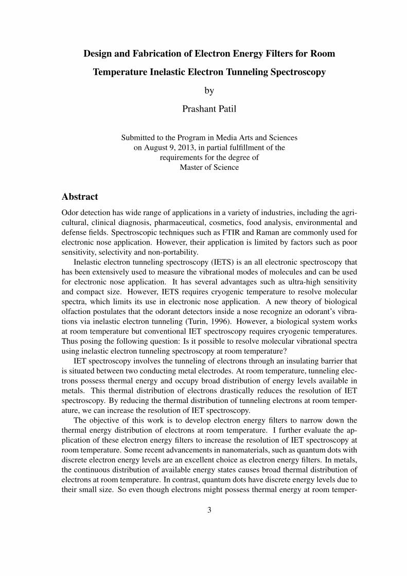
Design and Fabrication of Electron Energy Filters for Room
Temperature Inelastic Electron Tunneling Spectroscopy
by
Prashant Patil
Submitted to the Program in Media Arts and Scienceson August 9, 2013, in partial fulfillment of the
requirements for the degree ofMaster of Science
AbstractOdor detection has wide range of applications in a variety of industries, including the agri-cultural, clinical diagnosis, pharmaceutical, cosmetics, food analysis, environmental anddefense fields. Spectroscopic techniques such as FTIR and Raman are commonly used forelectronic nose application. However, their application is limited by factors such as poorsensitivity, selectivity and non-portability.
Inelastic electron tunneling spectroscopy (IETS) is an all electronic spectroscopy thathas been extensively used to measure the vibrational modes of molecules and can be usedfor electronic nose application. It has several advantages such as ultra-high sensitivityand compact size. However, IETS requires cryogenic temperature to resolve molecularspectra, which limits its use in electronic nose application. A new theory of biologicalolfaction postulates that the odorant detectors inside a nose recognize an odorant’s vibra-tions via inelastic electron tunneling (Turin, 1996). However, a biological system worksat room temperature but conventional IET spectroscopy requires cryogenic temperatures.Thus posing the following question: Is it possible to resolve molecular vibrational spectrausing inelastic electron tunneling spectroscopy at room temperature?
IET spectroscopy involves the tunneling of electrons through an insulating barrier thatis situated between two conducting metal electrodes. At room temperature, tunneling elec-trons possess thermal energy and occupy broad distribution of energy levels available inmetals. This thermal distribution of electrons drastically reduces the resolution of IETspectroscopy. By reducing the thermal distribution of tunneling electrons at room temper-ature, we can increase the resolution of IET spectroscopy.
The objective of this work is to develop electron energy filters to narrow down thethermal energy distribution of electrons at room temperature. I further evaluate the ap-plication of these electron energy filters to increase the resolution of IET spectroscopy atroom temperature. Some recent advancements in nanomaterials, such as quantum dots withdiscrete electron energy levels are an excellent choice as electron energy filters. In metals,the continuous distribution of available energy states causes broad thermal distribution ofelectrons at room temperature. In contrast, quantum dots have discrete energy levels due totheir small size. So even though electrons might possess thermal energy at room temper-
3

ature, they can only occupy the discrete energy levels available in quantum dots. Hence,the thermal energy distribution of electrons can be narrowed down to the energy levelsavailable in quantum dots.
The electron energy filter designed in this work, consists of a 2-dimensional array ofCdSe quantum dots of sizes around 2.5nm sandwiched between metal electrodes. Throughelectrical characterization of these devices, we can conclude that they can narrow downthermal distribution of electrons from 25meV down to around 10meV. However, to resolvethe molecular vibrational energy level at room temperature, thermal energy distribution ofelectrons should be less than 6.6meV. Since array of quantum dots results in formation ofenergy minibands, this work suggests that single quantum dot should be used instead ofarray of dots to improve the performance of electron energy filters. Moreover, the study ofelectron transport through single quantum dots done in this work suggests that the size ofthe dot should be less than 2.5nm to be used in room temperature IET spectroscopy.
Interestingly, this length scale is consistent with the size of donor and acceptor sitesin odorant receptors potentially explaining how these receptors could be able to resolvemolecular spectra at room temperatures.
Thesis Supervisor: Prof. Neil GershenfeldTitle: Director, MIT Center for Bits and Atoms
4
Design and Fabrication of Electron Energy Filters for Room
Temperature Inelastic Electron Tunneling Spectroscopy
by
Prashant Patil
The following people served as readers for this thesis:
Thesis Reader . . . . . . . . . . . . . . . . . . . . . . . . . . . . . . . . . . . . . . . . . . . . . . . . . . . . . . .Joseph M. Jacobson
Associate Professor of Media Arts and SciencesProgram in Media Arts and Sciences
Thesis Reader . . . . . . . . . . . . . . . . . . . . . . . . . . . . . . . . . . . . . . . . . . . . . . . . . . . . . . .Andreas Mershin
Research ScientistMIT Center for Bits and Atoms
5

6

Acknowledgments
I thank Neil Gershenfeld, my thesis advisor, for his guidance, for teaching me how to do
research. For buying me cool toys and letting me play with exciting one. Your guidance
has been invaluable in bringing this work to fruition.
I thank Joe Jacobson, every conversation I have had with you has been enlightening,
empowering, refreshing, provocative, and always instructive.
I thank Andreas Mershin, a long a steadfast critic and ultimately a guiding hand. You
have added additional focus on questions relating to this work.
I thank Luca, for getting me thinking about the problems in this thesis. Without you,
this thesis would have been about some other topic entirely.
I thank Nadya, you have been instrumental in my journey from IIT to MIT. When I
first met you in a workshop in Pune, I would have never thought that I would someday be
working with you.
I thank John D and Tom, for shop training’s and keeping us safe.
I thank Joe Murphy, you have always manage to sort out things for us. Thanks for
considering our carelessness as your own last minute emergency
I thank Ryan, for ordering long list of items and always helping skinny grad student
I thank Theresa, for taking time to chat with us and reminding us life beyond lab.
Feeding us with delicious food.
I thank Kenny, you have always been available for valuable suggestion on making things
I would like to thank Kurt Broderick mMrk Mondol for assisting me in learning the
various processes and systems in the microelectronics technology laboratory (MTL).
In addition a thank you to Professor K. W. Hipps of Washington State University for
valuable suggestions on fabrication of IETS devices.
Special gratitude must go to Charles Fracchia, Noah Jakimo, Thomas Duval, Sam
Calisch, Will Langford, James Pelletier, Lisa and Divya for there direct and indirect help
in this work. – thank you all.
7

8
Contents
1 Introduction 17
1.1 Inelastic Electron Tunneling Spectroscopy . . . . . . . . . . . . . . . . . . . . . . 18
1.2 Theory of Inelastic Electron Tunneling Spectroscopy . . . . . . . . . . . . . . . . 19
1.3 Electron Energy Filters for Room Temperature IETS . . . . . . . . . . . . . . . . 22
1.4 Scope of Thesis . . . . . . . . . . . . . . . . . . . . . . . . . . . . . . . . . . . . 23
2 Fabrication of Al−Al2O3−HCOOH−Pb Tunneling Device 27
2.1 Substrate Cleaning . . . . . . . . . . . . . . . . . . . . . . . . . . . . . . . . . . 28
2.2 Aluminum Deposition . . . . . . . . . . . . . . . . . . . . . . . . . . . . . . . . 28
2.3 Growth of Aluminum Oxide . . . . . . . . . . . . . . . . . . . . . . . . . . . . . 28
2.3.1 Growth of Aluminum Oxide using Oxygen Plasma . . . . . . . . . . . . . 29
2.4 Doping of Aluminum Oxide . . . . . . . . . . . . . . . . . . . . . . . . . . . . . 30
3 Inelastic Electron Tunneling Spectrometer 33
3.1 Theory of IETS Spectrometer Design . . . . . . . . . . . . . . . . . . . . . . . . 33
3.2 Design of IETS Spectrometer . . . . . . . . . . . . . . . . . . . . . . . . . . . . . 35
3.3 Inelastic Electron Tunneling Spectra of Al−Al2O3−HCOOH−Pb Device . . . . 37
4 Thermal Broadening of IETS Peaks 43
4.1 Theory of Thermal Broadening of IETS Peaks . . . . . . . . . . . . . . . . . . . . 44
4.1.1 IETS Peak-width at Various Temperature . . . . . . . . . . . . . . . . . . 46
9
4.2 Maximum Temperature to Resolve IETS peaks . . . . . . . . . . . . . . . . . . . 47
5 Theory of Quantum Dots Electron Energy Filters 53
5.1 Current-Voltage Characteristics of QDs Array . . . . . . . . . . . . . . . . . . . . 55
5.2 Elastic Tunneling Through QDs Arrays . . . . . . . . . . . . . . . . . . . . . . . 55
5.3 Inelastic Tunneling Through QDs Array . . . . . . . . . . . . . . . . . . . . . . . 56
5.4 Current Density Through QDs Array . . . . . . . . . . . . . . . . . . . . . . . . . 57
6 Fabrication of CdSe QDs Electron Energy Filters 61
6.1 Introduction . . . . . . . . . . . . . . . . . . . . . . . . . . . . . . . . . . . . . . 61
6.2 Fabrication and of ITO-QDs-Ag Devices . . . . . . . . . . . . . . . . . . . . . . . 62
6.3 Current-Voltage Characteristics of ITO−Al2O2−CdSeQDs−Ag Devices . . . . . 63
6.4 Fabrication of Al−Al2O3−QDs−Pb Tunneling Device . . . . . . . . . . . . . . 68
6.5 Current-Voltage Characteristics of Al−Al2O3−QDs−Pb Devices . . . . . . . . 69
7 Electron Transport through Single CdSe Quantum dot 75
7.1 Current-Sensing Atomic Force Spectroscopy . . . . . . . . . . . . . . . . . . . . . 75
7.2 AFM Imaging of CdSe Quantum Dots . . . . . . . . . . . . . . . . . . . . . . . . 76
7.3 Current-Voltage Spectroscopy of Single CdSe Quantum Dot . . . . . . . . . . . . 76
7.4 Result and Discussion . . . . . . . . . . . . . . . . . . . . . . . . . . . . . . . . . 77
8 Summary and Conclusion 81
8.1 Summary . . . . . . . . . . . . . . . . . . . . . . . . . . . . . . . . . . . . . . . 81
8.2 Conclusion . . . . . . . . . . . . . . . . . . . . . . . . . . . . . . . . . . . . . . 83
8.3 Discussion - Quantum dots vs Odorant Receptors . . . . . . . . . . . . . . . . . . 84
8.4 Future Works . . . . . . . . . . . . . . . . . . . . . . . . . . . . . . . . . . . . . 85
10

List of Figures
1.1 conventional metal-insulator-metal IETS Devices . . . . . . . . . . . . . . . . . . 18
1.2 Comparison of vibrational energy peaks observed in IETS, FTIR and Raman spec-
troscopy [4] . . . . . . . . . . . . . . . . . . . . . . . . . . . . . . . . . . . . . . 19
1.3 Band diagram of metal-insulator-metal device . . . . . . . . . . . . . . . . . . . . 20
1.4 Schematic representation of Current-Voltage characteristics of metal-insulator-metal
tunneling junction . . . . . . . . . . . . . . . . . . . . . . . . . . . . . . . . . . . 21
1.5 Schematic representation of change in conductance of M− I−A−M devices and
observation of IETS Peaks . . . . . . . . . . . . . . . . . . . . . . . . . . . . . . 25
2.1 Schematic diagram of Metal-Insulator-Metal Inelastic Tunneling Device . . . . . . 27
2.2 Current-Voltage Characteristics of an Al−Al2O3−Pb Device . . . . . . . . . . . 31
3.1 Schematic circuit diagram of IETS Spectrometer . . . . . . . . . . . . . . . . . . 35
3.2 Block diagram of IETS spectrometer design . . . . . . . . . . . . . . . . . . . . . 36
3.3 Current-Voltage Characteristics of Al−Al2O3−HCOOH−Pb Devices . . . . . . 38
3.4 Firs derivative dVdI measured for Al−Al2O3−HCOOH−Pb Devices . . . . . . . . 39
3.5 Measured IETS peaks on Al−Al2O3−HCOOH−Pb Devices . . . . . . . . . . . 40
3.6 d2VdI2 w.r.t current plot of Al−Al2O3−HCOOH −Pb devices at low temperature
and room temperature . . . . . . . . . . . . . . . . . . . . . . . . . . . . . . . . 41
4.1 Band diagram of metal− insulator−metal devices at low temperature and at room
temperature . . . . . . . . . . . . . . . . . . . . . . . . . . . . . . . . . . . . . . 44
11
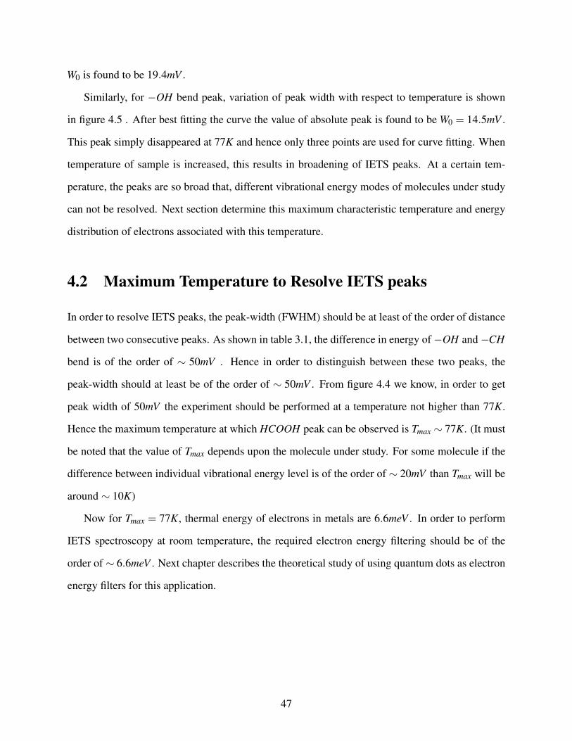
4.2 Measured IETS peaks on Al−Al2O3−HCOOH −Pb Devices at T = 4.2K and
T = 10K . . . . . . . . . . . . . . . . . . . . . . . . . . . . . . . . . . . . . . . . 48
4.3 Measured IETS peaks on Al−Al2O3−HCOOH −Pb Devices at T = 4.2K and
T = 10K . . . . . . . . . . . . . . . . . . . . . . . . . . . . . . . . . . . . . . . . 49
4.4 Plot of IETS peak width (W) w.r.t. Temperature for −CH stretch peak . . . . . . . 50
4.5 Plot of IETS peak width (W) w.r.t. Temperature for −OH band peak . . . . . . . . 51
5.1 Energy Level Diagrams of (a) Single CdSe QD and (b) formation of energy mini-
bands in 2-dimentianal array of CdSe QDs . . . . . . . . . . . . . . . . . . . . . . 59
6.1 Schematic Diagram of device structure of ITO-QDs-Ag Devices . . . . . . . . . . 61
6.2 Band diagram of M-I-QD-I-M Devices . . . . . . . . . . . . . . . . . . . . . . . 62
6.3 Scanning electron microscope image of CdSe quantum dots spin coated on ITO
substrate . . . . . . . . . . . . . . . . . . . . . . . . . . . . . . . . . . . . . . . . 63
6.4 Schematic representation of electrical connection made on ITO−Al2O3−CdSeQDs−
Ag Devices . . . . . . . . . . . . . . . . . . . . . . . . . . . . . . . . . . . . . . 63
6.5 Current-Voltage Characteristics of three different ITO−QDs−Ag Devices . . . . 64
6.6 Band Diagram of Ag−CdSeQDs Interface and formation of Schottky barrier . . . 65
6.7 Band diagram of ITO-QDs interface . . . . . . . . . . . . . . . . . . . . . . . . . 66
6.8 Band diagram of theITO−Al2O3(5nm)−CdSeQDs( 80nm)−Al2O3(5nm)−Ag
Devices . . . . . . . . . . . . . . . . . . . . . . . . . . . . . . . . . . . . . . . . 67
6.9 Current-Voltage Characteristics ofAl−Al2O3−QDs−Pb Devices . . . . . . . . . 70
6.10 Current-Voltage characteristics of Al − Al2O3 −QDs− Pb devices which were
cooled to 4.2K and then brought to room temperature for measurement . . . . . . . 71
6.11 dIdV vs voltage measurement of Al−Al2O3−QDs−Pb devices which were cooled
to 4.2K and then brought to room temperature for measurement . . . . . . . . . . 72
6.12 Current-Voltage Characteristics ofAl−Al2O3−QDs−Pb Devices for Temperature
Cycle . . . . . . . . . . . . . . . . . . . . . . . . . . . . . . . . . . . . . . . . . 73
12

7.1 AFM image of CdSe Quantum dots spin coated on gold coated mica substrate . . . 77
7.2 STM tip over a quantum dot for Current-Voltage Spectroscopy . . . . . . . . . . . 78
7.3 Schematic diagram of Current-Voltage Spectroscopy of individual QDs . . . . . . 78
7.4 Circuit Diagram of current pre-amp used in IV Spectroscopy system . . . . . . . . 79
7.5 Current-Voltage Spectroscopy of individual CdSe QDs using CSAFM . . . . . . . 79
8.1 Schematic of the proposed IETS mechanism inside odorant receptors for molecular
spectroscopy [1] . . . . . . . . . . . . . . . . . . . . . . . . . . . . . . . . . . . . 85
13

14
List of Tables
2.1 Growth of Al2O3 with different experimental parameters . . . . . . . . . . . . . . 30
3.1 Peak position and corresponding identified vibrational mode for impurities in Al−
Al2O3−HCOOH−Pb Devices . . . . . . . . . . . . . . . . . . . . . . . . . . . 39
4.1 IETS peak-width w.r.t. temperature . . . . . . . . . . . . . . . . . . . . . . . . . . 46
6.1 Resistance and Capacitance of M− I−QDs−M Devices . . . . . . . . . . . . . . 69
15

16
Chapter 1
Introduction
The major applications of odor detection are in the agricultural industry, clinical diagnosis, phar-
maceutical, cosmetics, food analysis, environmental and defense. In food industry, it is used to
check quality of ingredients and spoilage, to monitor livestock and poultry facilities. In biomedi-
cal industry it is used for diagnosis of variety of diseases by breath analysis. Molecular vibrational
spectroscopy is commonly used for odorant recognition. The vibrations of the chemical bonds in
a molecule occur at specific frequencies. This vibrational spectrum is unique for every molecule
and acts as a molecular fingerprint. Thus vibrational spectrum of a molecule be used for molecu-
lar identification and characterization. Optical spectroscopic techniques such as FTIR and Raman
are commonly used to measure vibrational spectrum of molecules. But these techniques require
complex optics, are bulky and consume high power. This limits there usability in electronic nose
application.
Inelastic electron tunneling spectroscopy (IETS) is a type of vibrational spectroscopy that ex-
tracts the vibrational spectra of molecules adsorbed into the insulator layer of a tunnel junction.
As opposed to other vibrational spectroscopy, IETS does not require complex optics and has low
power consumption. It is also an all electronic spectroscopy so even optically forbidden transitions
which are invisible in FTIR and Raman can also be observed in inelastic electron tunneling spec-
troscopy. Because of its ultra-high sensitivity, low power consumption and portability, IETS is an
17
excellent candidate for electronic nose application.
1.1 Inelastic Electron Tunneling Spectroscopy
The phenomenon of Inelastic electron tunneling was first observed by Jaklevic and Lamb[2] in
1966 . It was observed that the conductance of a metal-insulator-metal junction increases at a
certain characteristics bias voltages. These voltages correspond to the vibrational energy levels of
the impurity molecules adsorbed in the insulating tunneling junction. It was found that tunneling
electrons were actually interacting with the vibrational states of impurity molecules.
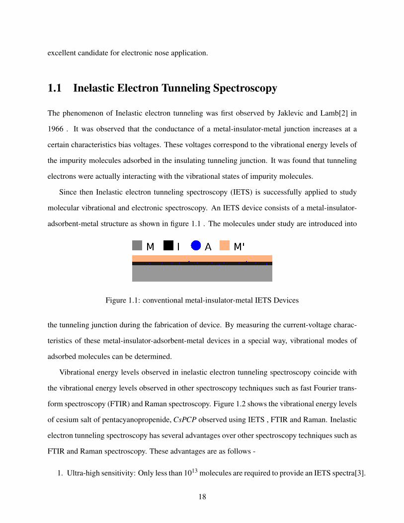
Since then Inelastic electron tunneling spectroscopy (IETS) is successfully applied to study
molecular vibrational and electronic spectroscopy. An IETS device consists of a metal-insulator-
adsorbent-metal structure as shown in figure 1.1 . The molecules under study are introduced into
Figure 1.1: conventional metal-insulator-metal IETS Devices
the tunneling junction during the fabrication of device. By measuring the current-voltage charac-
teristics of these metal-insulator-adsorbent-metal devices in a special way, vibrational modes of
adsorbed molecules can be determined.
Vibrational energy levels observed in inelastic electron tunneling spectroscopy coincide with
the vibrational energy levels observed in other spectroscopy techniques such as fast Fourier trans-
form spectroscopy (FTIR) and Raman spectroscopy. Figure 1.2 shows the vibrational energy levels
of cesium salt of pentacyanopropenide, CsPCP observed using IETS , FTIR and Raman. Inelastic
electron tunneling spectroscopy has several advantages over other spectroscopy techniques such as
FTIR and Raman spectroscopy. These advantages are as follows -
1. Ultra-high sensitivity: Only less than 1013 molecules are required to provide an IETS spectra[3].
18
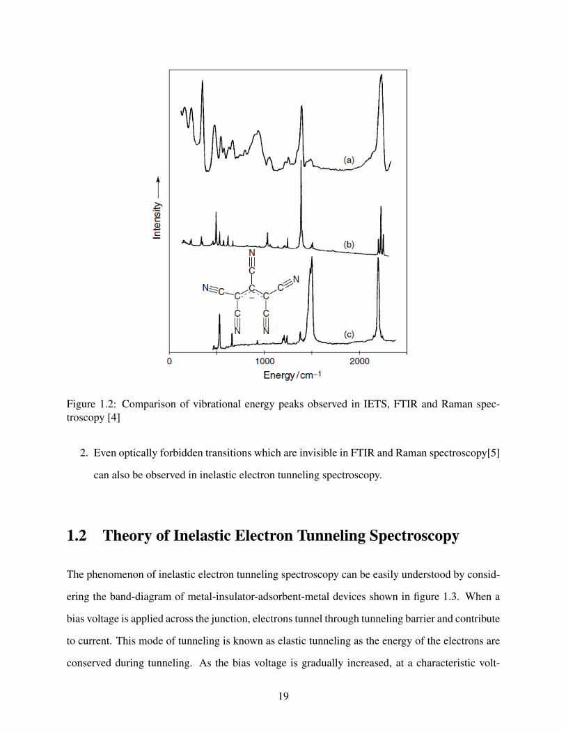
Figure 1.2: Comparison of vibrational energy peaks observed in IETS, FTIR and Raman spec-troscopy [4]
2. Even optically forbidden transitions which are invisible in FTIR and Raman spectroscopy[5]
can also be observed in inelastic electron tunneling spectroscopy.
1.2 Theory of Inelastic Electron Tunneling Spectroscopy
The phenomenon of inelastic electron tunneling spectroscopy can be easily understood by consid-
ering the band-diagram of metal-insulator-adsorbent-metal devices shown in figure 1.3. When a
bias voltage is applied across the junction, electrons tunnel through tunneling barrier and contribute
to current. This mode of tunneling is known as elastic tunneling as the energy of the electrons are
conserved during tunneling. As the bias voltage is gradually increased, at a characteristic volt-
19

Figure 1.3: Band diagram of metal-insulator-metal device
age, electrons now have sufficient energy to excite the vibrational energy level of the adsorbed
molecules. These electrons during tunneling can loose part of their energy to excite the vibrational
energy level of adsorbed molecules. This mode of tunneling is know as inelastic tunneling as
energy of the electrons are not conserved. This process is schematically shown in figure 1.3(b).
Once the applied bias voltage exceeds this characteristics voltage, the total tunneling current
now consist of both elastic tunneling current and inelastic tunneling current. This addition of extra
channel of inelastic tunneling current results in an increase in the conductance of these devices.
Figure 1.4 schematically shows the current-voltage characteristics of a metal-insulator-adsorbate-
metal device. For a bias voltage V < hve , the current only constitutes of elastic tunneling current.
When bias voltage exceeds hve which is the vibrational energy level of the adsorbed molecule, the
current constitute of both elastic and inelastic tunneling current. This increase in conductance
results in change in slop of current-voltage curve. Since inelastic current constitutes only 1% of
the total current, this change in slop is not visible in a practical current voltage characteristics.
This small change in conductance i.e. change in slop of IV curve appears as step in dI/dV vs
V plot and as a peak in d2I/dV 2 vs V plot as shown in figure 1.5(a) . Since peak position can easily
be identified as compare to change in slop in IV curve or steps in dI/dV vs V , the plot between
20
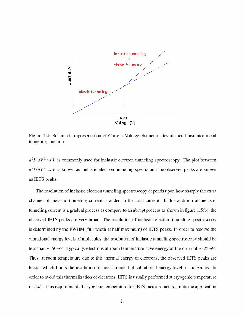
Figure 1.4: Schematic representation of Current-Voltage characteristics of metal-insulator-metaltunneling junction
d2I/dV 2 vs V is commonly used for inelastic electron tunneling spectroscopy. The plot between
d2I/dV 2 vs V is known as inelastic electron tunneling spectra and the observed peaks are known
as IETS peaks.
The resolution of inelastic electron tunneling spectroscopy depends upon how sharply the extra
channel of inelastic tunneling current is added to the total current. If this addition of inelastic
tunneling current is a gradual process as compare to an abrupt process as shown in figure 1.5(b), the
observed IETS peaks are very broad. The resolution of inelastic electron tunneling spectroscopy
is determined by the FWHM (full width at half maximum) of IETS peaks. In order to resolve the
vibrational energy levels of molecules, the resolution of inelastic tunneling spectroscopy should be
less than ∼ 50mV . Typically, electrons at room temperature have energy of the order of ∼ 25mV .
Thus, at room temperature due to this thermal energy of electrons, the observed IETS peaks are
broad, which limits the resolution for measurement of vibrational energy level of molecules. In
order to avoid this thermalization of electrons, IETS is usually performed at cryogenic temperature
( 4.2K). This requirement of cryogenic temperature for IETS measurements, limits the application
21
of IETS for sensing application such as gas sensors and electronic nose.
1.3 Electron Energy Filters for Room Temperature IETS
The resolution of IET spectroscopy is temperature dependent. In order to resolve molecular vibra-
tions using IETS, experiment should be performed at cryogenic temperature. At room temperature,
tunneling electrons possess thermal energy and occupy broad distribution of energy levels avail-
able in metals. This thermal distribution of electrons results in thermal broadening on IETS peak
which drastically reduced the resolution of IETS spectroscopy.
A new theory of biological olfaction postulates that the odorant detectors inside nose recog-
nizes an odorant’s vibrations via inelastic electron tunneling[1]. A biological system must work at
ambient or body temperature, i.e. at 300K. When IETS is performed between metal electrodes, the
tunneling junction is cooled to cryogenic temperatures to increase resolution to resolve vibrational
energy level of molecules. This pose a question “ Is it possible to resolve molecular vibrational
spectra using inelastic electron tunneling spectroscopy at room temperature?”
In order to perform inelastic electron tunneling spectroscopy at room temperature with a reso-
lution to measure vibrational energy levels of molecules, we have to minimize the thermalization
of electrons at room temperature. In metals, continuous distribution of energy states are available.
These energy states can be occupied by thermalized electrons resulting in broad thermal distribu-
tion of electrons around Fermi level of metals. This thermal distribution of electrons results in
thermal broadening of IETS peaks. This reduces the resolution of IETS at room temperature.
The objective of this work is to develop “electron energy filters” to narrow down the thermal
energy distribution of electrons at room temperature. Quantum dots due to their small size have
discrete energy levels. So even though electrons in quantum dots can possess thermal energy
at room temperature, they can only occupy the discrete energy states available in quantum dots.
Hence, the thermal energy distribution of electrons can be narrowed down to only energy levels
available in quantum dots. In other word, quantum dots act as electron energy filter to narrow down
22
thermal distribution of electrons.
1.4 Scope of Thesis
In my thesis, I first discuss fabrication and characterization of inelastic electron tunneling devices.
Chapter 2, describe fabrication of metal-insulator-metal inelastic tunneling devices. As we
know, inelastic electron tunneling spectroscopy involves direct measurement of d2IdI2 . Chapter 3,
describes the instrumentation developed to directly measure d2IdI2 using standard modulation tech-
nique. This system is named as inelastic electron tunneling spectrometer. In order to determine
the required electron energy filtering, to resolve vibrational energy levels of molecules using IETS,
thermal broadening of IETS peaks is studied. Chapter 4, discuss theoretical prediction of thermal
broadening and compares it with observed IETS peak-width at various temperatures.
Once the required electron energy filtering (i.e Q-factor of energy filter) is determined, electron
energy filters are designed using quantum dots. Chapter 5, discuss the theoretical model of a
2dimensional array of quantum dots that can be used as electron energy filters. This 2D array of
QDs is modeled as a resonant tunneling diode with minibands. Chapter 6, presents fabrication of
quantum dots energy filters using CdSe QDs. These filter consist of ITO−Al2O3−CdSeQDs−Pb
and Al−Al2O3−CdSeQDs−Pb device structure. Current-voltage measurement is performed on
these devices to determine the Q-factor (i.e. extent of energy filtering) of these CdSe QDs energy
filters.
Chapter 7, describes using single CdSe QDs for electron energy filters. Current-sensing atomic
force microscopy in IV spectroscopy mode is used to study the electron transport through single
QDs at room temperature. This current-voltage measurement is then used to determine Q-factor of
single CdSe QDs energy filter.
Finally, Chapter 8 compares the electron energy filtering required to perform high resolution
inelastic electron tunneling spectroscopy obtained from Chapter 4 with achievable energy filtering
using array of CdSe QDs (Chapter 6) and single CdSe QDs (Chapter 7). My thesis conclude with
23

discussing highest resolution achievable using quantum dots energy filter and suggest future work
relating to further improving the resolution of inelastic electron tunneling spectroscopy at room
temperature.
24
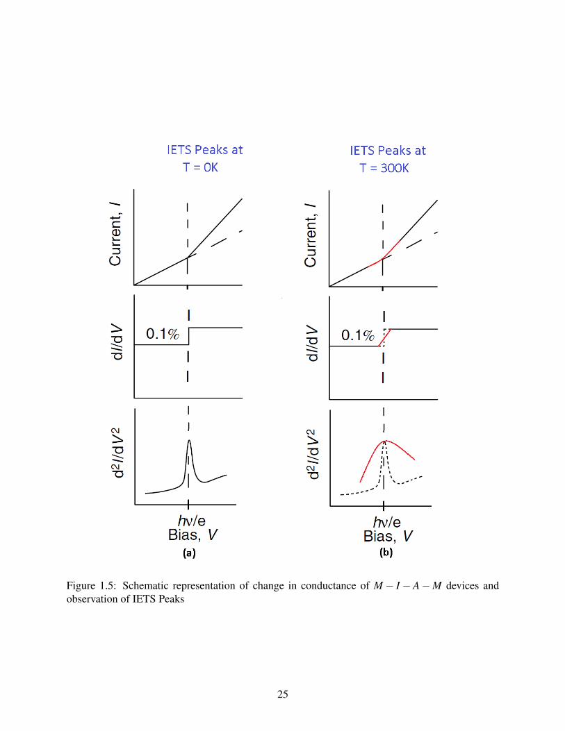
Figure 1.5: Schematic representation of change in conductance of M− I − A−M devices andobservation of IETS Peaks
25

26
Chapter 2
Fabrication of Al−Al2O3−HCOOH−Pb
Tunneling Device
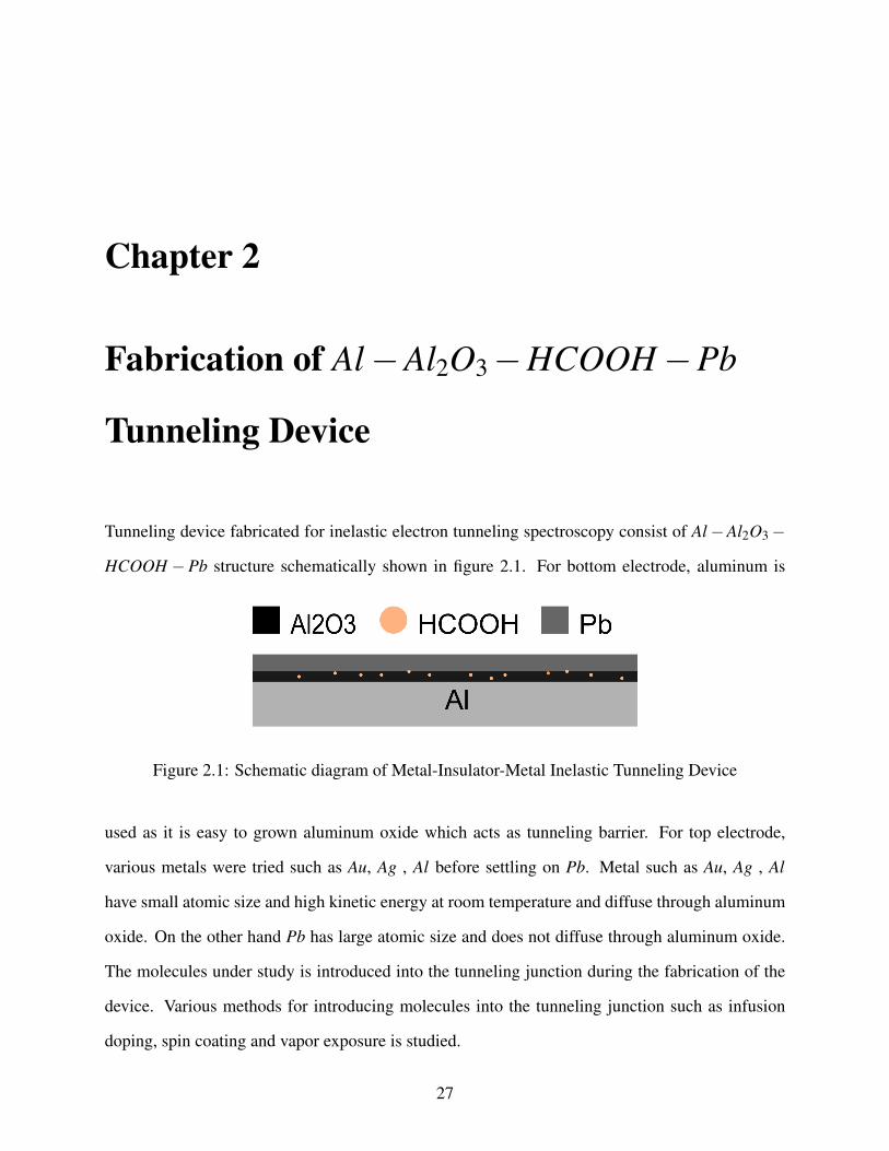
Tunneling device fabricated for inelastic electron tunneling spectroscopy consist of Al−Al2O3−
HCOOH −Pb structure schematically shown in figure 2.1. For bottom electrode, aluminum is
Figure 2.1: Schematic diagram of Metal-Insulator-Metal Inelastic Tunneling Device
used as it is easy to grown aluminum oxide which acts as tunneling barrier. For top electrode,
various metals were tried such as Au, Ag , Al before settling on Pb. Metal such as Au, Ag , Al
have small atomic size and high kinetic energy at room temperature and diffuse through aluminum
oxide. On the other hand Pb has large atomic size and does not diffuse through aluminum oxide.
The molecules under study is introduced into the tunneling junction during the fabrication of the
device. Various methods for introducing molecules into the tunneling junction such as infusion
doping, spin coating and vapor exposure is studied.
27
2.1 Substrate Cleaning
Standard microscope glass substrate is cut into small pieces of dimension10mmx10mm. Following
cleaning procedure is performed to remove organic impurities and dust from the substrate.
1. Substrate is cleaned with acetone in ultrasonic bath for 60s to remove organic impurities.
2. Before acetone dries out, its washed away with isopropyl alcohol.
3. The substrate is then rinsed thoroughly with DI water and dried by blowing clean nitrogen.
4. These substrate are then tested for low temperature tolerance by quickly immersing them on
liquid nitrogen. Those pieces which were cracked during immersion were discarded and rest
are used for device fabrication.
2.2 Aluminum Deposition
Aluminum is deposited using Auto 306 thermal evaporation system. In order to deposit 1mm
wide aluminum strip on glass substrate, shadow mask is used. The deposition system consist of
turbo-molecular pump backed by rotary pump to create high vacuum. An alumina coated tungsten
boat is used to melt aluminum to avoid formation of aluminum-tungsten alloy. The system is
also fitted with thickness meter to measure the thickness of the deposited metal. For deposition,
the deposition chamber is first evacuated to base pressure of 3x10⁻⁶mbar and then deposition is
started at 1nm/s rate to deposit 100nm thick Al layer.
2.3 Growth of Aluminum Oxide
Aluminum oxide is grown on top of Al electrode using “exposure to air at room temperature” and
“plasma oxidation” process. For room temperature exposure, sample is kept in room temperature
in lab environment for 24 hours. These method grows native aluminum oxide with oxide thickness
of around ∼ 4nm. The disadvantage of growing oxide using this method is as follows
28
1. The oxide grown using this technique is contaminated with atmosphere impurities.
2. Grown aluminum oxides are not very dense and possess few pin holes. These pin holes leads
to shorting of the two metal electrodes destroying the devices. The success rate of devices
fabricated using this method is very low.
3. The devices take long time to fabricate and its difficult to fine control the thickness of the
grown aluminum oxide. Devices fabricated using this method suffer from poor reproducibil-
ity.
The other method which gave very good quality dense oxide, free from pin holes and impurity is
grown using oxygen plasma. This method is described in next section.
2.3.1 Growth of Aluminum Oxide using Oxygen Plasma
Anatech SP-100 plasma cleaner is used to grow aluminum oxide. The plasma chamber is connected
to an oxygen cylinder through a flow controller. The advantage of using this system is that the oxide
is very dense and is free from impurities. The thickness of grown oxide is controlled by controlling
Rf power, oxygen flow rate in plasma chamber and time of growth. The resistance of the device
depends upon the thickness of aluminum oxide and is used as quantitative estimate for thickness
of grown aluminum oxide. First, several samples are prepared by depositing 100nm of Al on pre-
cleaned glass substrate. Aluminum oxide is grown using different experimental parameters such as
Rf power, oxygen flow rate and time of growth. After the growth of a aluminum oxide, 200nm Pb is
deposited in cross electrode geometry perpendicular to aluminum electrode. For making electrical
contacts, indium soldering is used as it has very high affinity to glass. Once the contacts are made,
device resistance is measured using Agilent 34401A multimeter. Table2.1 tabulates various growth
parameters and observed resistance of fabricated devices.
Current-voltage measurement is taken using HP semiconductor analyzer. Figure shows a
current-voltage characteristics of an Al−Al2O3−Pb device.
29
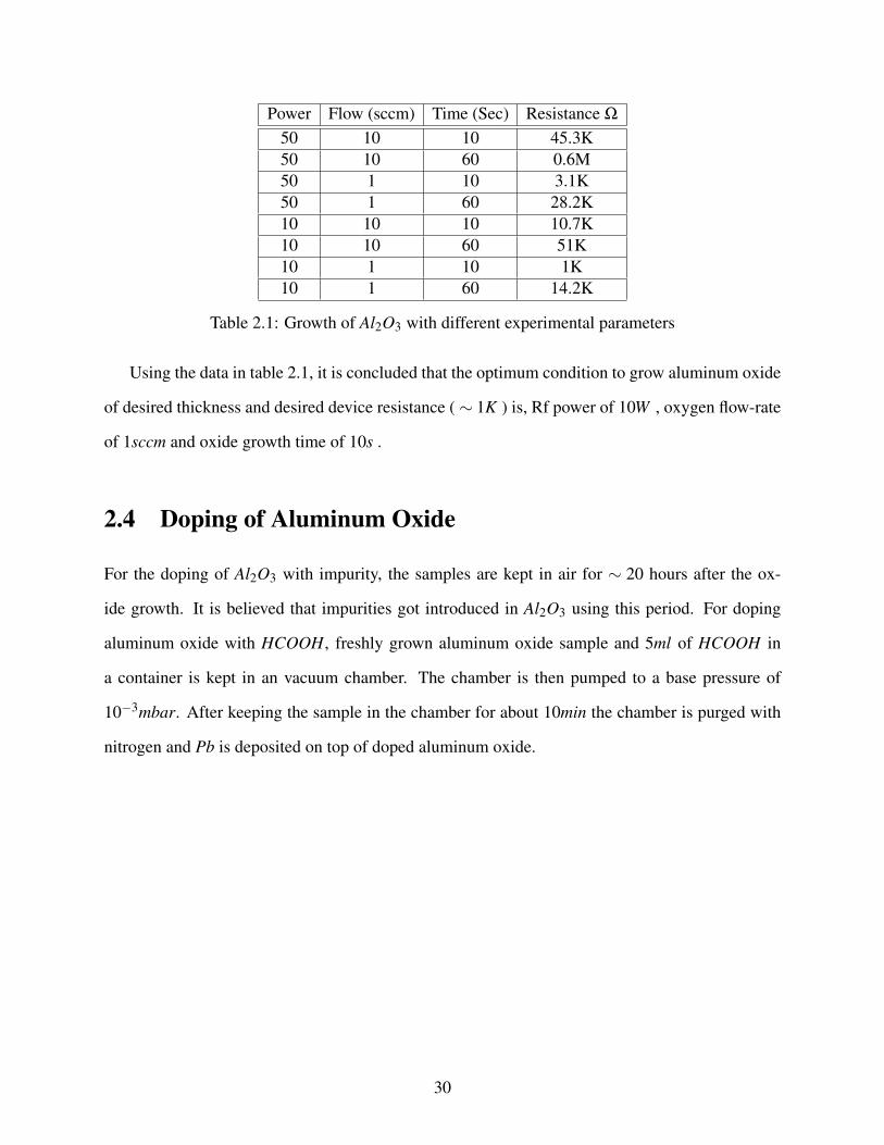
Power Flow (sccm) Time (Sec) Resistance Ω
50 10 10 45.3K50 10 60 0.6M50 1 10 3.1K50 1 60 28.2K10 10 10 10.7K10 10 60 51K10 1 10 1K10 1 60 14.2K
Table 2.1: Growth of Al2O3 with different experimental parameters
Using the data in table 2.1, it is concluded that the optimum condition to grow aluminum oxide
of desired thickness and desired device resistance ( ∼ 1K ) is, Rf power of 10W , oxygen flow-rate
of 1sccm and oxide growth time of 10s .
2.4 Doping of Aluminum Oxide
For the doping of Al2O3 with impurity, the samples are kept in air for ∼ 20 hours after the ox-
ide growth. It is believed that impurities got introduced in Al2O3 using this period. For doping
aluminum oxide with HCOOH, freshly grown aluminum oxide sample and 5ml of HCOOH in
a container is kept in an vacuum chamber. The chamber is then pumped to a base pressure of
10−3mbar. After keeping the sample in the chamber for about 10min the chamber is purged with
nitrogen and Pb is deposited on top of doped aluminum oxide.
30
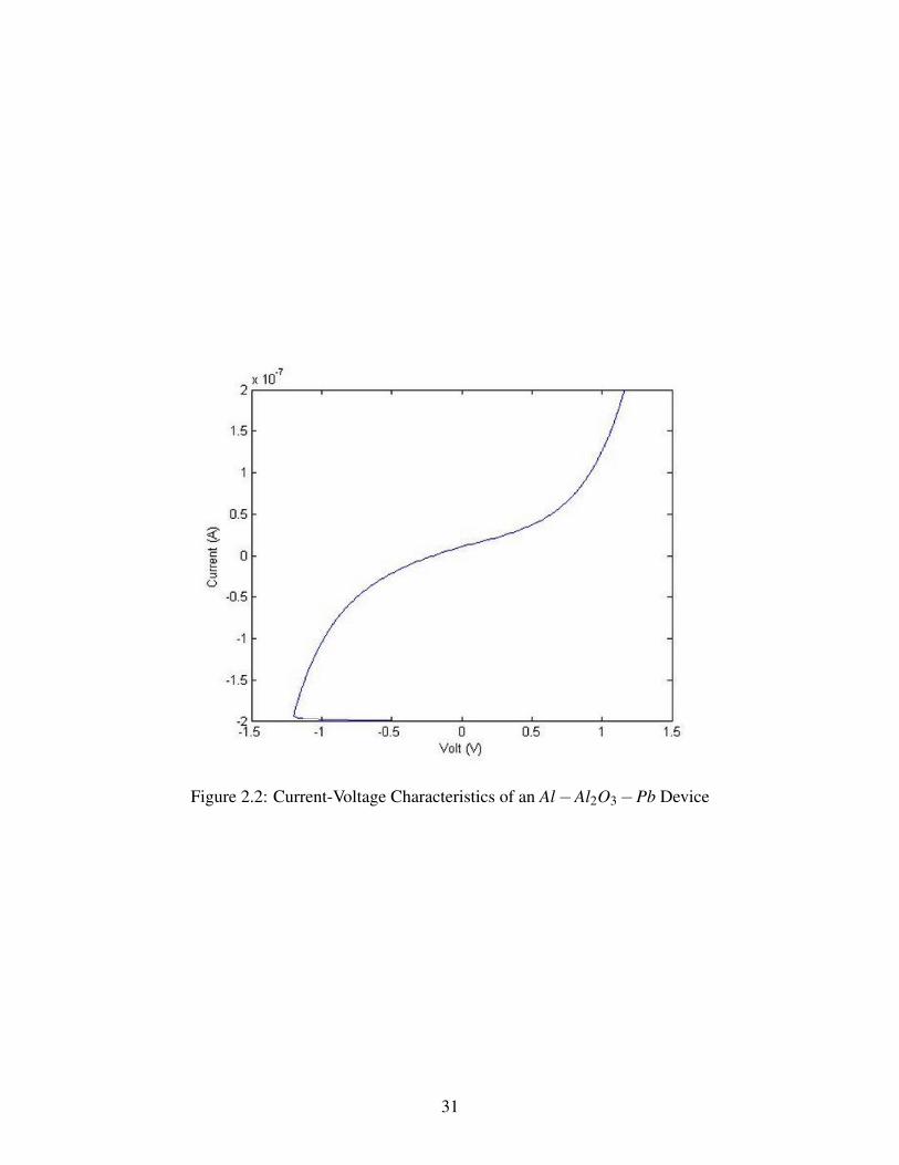
Figure 2.2: Current-Voltage Characteristics of an Al−Al2O3−Pb Device
31

32
Chapter 3
Inelastic Electron Tunneling Spectrometer
Inelastic electron tunneling spectroscopy requires measurement of second derivative of current-
voltage characteristics. Instrumentation is developed to measure second derivative of I-V curve
using standard modulation technique. An AC/DC current source is used to bias the device under
study. The DC voltage across the device is measured using Keithley 2182S nanovoltmeter. For
measurement of first and second derivative of current w.r.t voltage, two digital lock-in amplifiers
are used. This chapter first discuss theory of modulation technique used for direct measurement
of d2IdV 2 followed by describing actual instrumentation used for measurement. Chapter concludes
with presenting measurement inelastic tunneling spectra of Al−Al2O3−HCOOH −Pb device
fabricated in last chapter.
3.1 Theory of IETS Spectrometer Design
Consider a dc current Ib modulated with small ac current icos(ωt) , is allowed to pass through the
device. The total current through the device is I = Ib+ icos(ωt) and the voltage drop is VD(I). The
Taylor series expansion of the voltage across the device V (I) about the dc bias current Ib is given
by
33

VD (I) =V (Ib)+
(dVdI
)(I− Ib)+
(12
)(d2VdI2
)(I− Ib)
2 + .....
⇒VD (I) =V (I)+(
dVdI
)icos(ωt)+
(12
)(d2VdI2
)[icos(ωt)]2 + .....
⇒VD (I) =V (I)+(
dVdI
)icos(ωt)−
(14
)(d2VdI2
)i2cos(2ωt)+ .....
Now, lock-in amplifiers tuned at ω and 2ω will respectively measure (rms values)
Vω =1√2
(dVdI
)i
V2ω =− 1√2
(14
)(d2VdI2
)i2
Once we have the value of(dV
dI
)and
(d2VdI2
), IETS signal d2I
dV 2 can be calculated using the
following relation
d2IdV 2 =−
(d2VdI2
)(dIdV
)3
If we assume that the bias voltage is limited to 0.5V then the value of( dI
dV
)is constant and
above equation can be reduced to
d2IdV 2 =−k
(d2VdI2
)
Since in such cases,(
d2IdV 2
)and
(d2VdI2
)are qualitatively same, in our reported data we have
34
directly plotted the value of(
d2VdI2
)or voltage V2ω measured from lock-in amplifier tuned at fre-
quency 2ω
3.2 Design of IETS Spectrometer
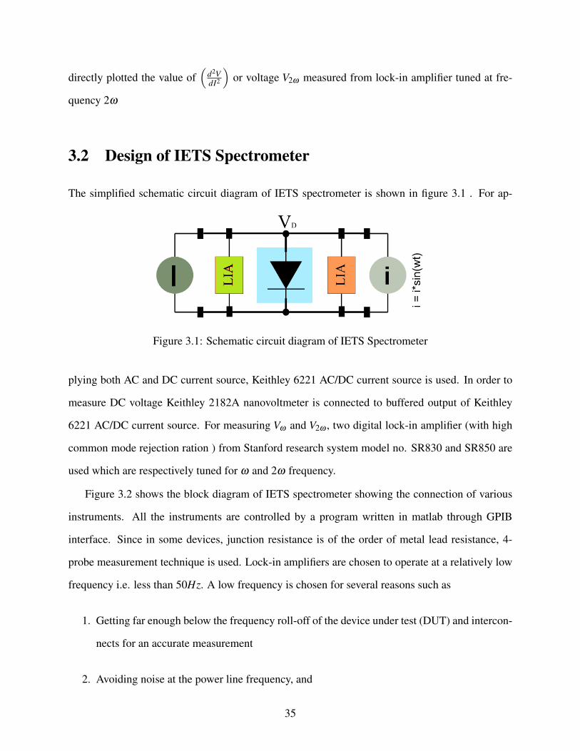
The simplified schematic circuit diagram of IETS spectrometer is shown in figure 3.1 . For ap-
Figure 3.1: Schematic circuit diagram of IETS Spectrometer
plying both AC and DC current source, Keithley 6221 AC/DC current source is used. In order to
measure DC voltage Keithley 2182A nanovoltmeter is connected to buffered output of Keithley
6221 AC/DC current source. For measuring Vω and V2ω , two digital lock-in amplifier (with high
common mode rejection ration ) from Stanford research system model no. SR830 and SR850 are
used which are respectively tuned for ω and 2ω frequency.
Figure 3.2 shows the block diagram of IETS spectrometer showing the connection of various
instruments. All the instruments are controlled by a program written in matlab through GPIB
interface. Since in some devices, junction resistance is of the order of metal lead resistance, 4-
probe measurement technique is used. Lock-in amplifiers are chosen to operate at a relatively low
frequency i.e. less than 50Hz. A low frequency is chosen for several reasons such as
1. Getting far enough below the frequency roll-off of the device under test (DUT) and intercon-
nects for an accurate measurement
2. Avoiding noise at the power line frequency, and
35
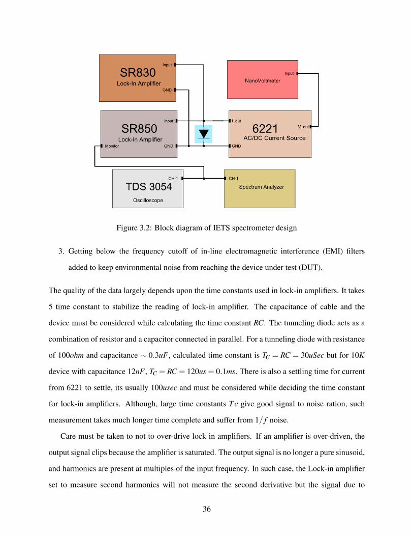
Figure 3.2: Block diagram of IETS spectrometer design
3. Getting below the frequency cutoff of in-line electromagnetic interference (EMI) filters
added to keep environmental noise from reaching the device under test (DUT).
The quality of the data largely depends upon the time constants used in lock-in amplifiers. It takes
5 time constant to stabilize the reading of lock-in amplifier. The capacitance of cable and the
device must be considered while calculating the time constant RC. The tunneling diode acts as a
combination of resistor and a capacitor connected in parallel. For a tunneling diode with resistance
of 100ohm and capacitance ∼ 0.3uF , calculated time constant is TC = RC = 30uSec but for 10K
device with capacitance 12nF , TC = RC = 120us = 0.1ms. There is also a settling time for current
from 6221 to settle, its usually 100usec and must be considered while deciding the time constant
for lock-in amplifiers. Although, large time constants T c give good signal to noise ration, such
measurement takes much longer time complete and suffer from 1/ f noise.
Care must be taken to not to over-drive lock in amplifiers. If an amplifier is over-driven, the
output signal clips because the amplifier is saturated. The output signal is no longer a pure sinusoid,
and harmonics are present at multiples of the input frequency. In such case, the Lock-in amplifier
set to measure second harmonics will not measure the second derivative but the signal due to
36
saturation of amplifier.
3.3 Inelastic Electron Tunneling Spectra of Al−Al2O3−HCOOH−
Pb Device
This section briefly describes fabrication of Al−Al2O3−HCOOH−Pb devices and presents in-
elastic electron tunneling spectra obtained from devices. For fabricating Al−Al2O3−HCOOH−
Pb devices, first the substrate is cleaned as described in section 2.1. 100nm aluminum is deposited
followed by oxygen RF-plasma oxidation at 10sccm oxygen flow rate, 10W RF power for 10s. The
device is then kept in air for ~20h before exposing it to HCOOH vapor for oxide doping. Final
resistance of the device is found be around ∼ 1K. For IETS measurement, electrical contacts are
made using indium solder and the sample is mounted inside the liquid helium cryostat.
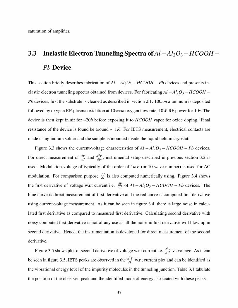
Figure 3.3 shows the current-voltage characteristics of Al−Al2O3−HCOOH −Pb devices.
For direct measurement of dVdI and d2V
dI2 , instrumental setup described in previous section 3.2 is
used. Modulation voltage of typically of the order of 1mV (or 10 wave number) is used for AC
modulation. For comparison purpose dVdI is also computed numerically using. Figure 3.4 shows
the first derivative of voltage w.r.t current i.e. dVdI of Al−Al2O3−HCOOH −Pb devices. The
blue curve is direct measurement of first derivative and the red curve is computed first derivative
using current-voltage measurement. As it can be seen in figure 3.4, there is large noise in calcu-
lated first derivative as compared to measured first derivative. Calculating second derivative with
noisy computed first derivative is not of any use as all the noise in first derivative will blow up in
second derivative. Hence, the instrumentation is developed for direct measurement of the second
derivative.
Figure 3.5 shows plot of second derivative of voltage w.r.t current i.e. d2VdI2 vs voltage. As it can
be seen in figure 3.5, IETS peaks are observed in the d2VdI2 w.r.t current plot and can be identified as
the vibrational energy level of the impurity molecules in the tunneling junction. Table 3.1 tabulate
the position of the observed peak and the identified mode of energy associated with these peaks.
37
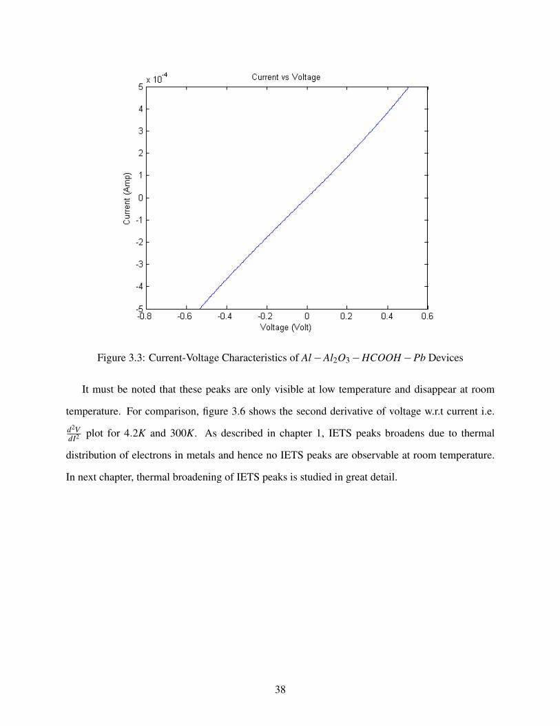
Figure 3.3: Current-Voltage Characteristics of Al−Al2O3−HCOOH−Pb Devices
It must be noted that these peaks are only visible at low temperature and disappear at room
temperature. For comparison, figure 3.6 shows the second derivative of voltage w.r.t current i.e.
d2VdI2 plot for 4.2K and 300K. As described in chapter 1, IETS peaks broadens due to thermal
distribution of electrons in metals and hence no IETS peaks are observable at room temperature.
In next chapter, thermal broadening of IETS peaks is studied in great detail.
38
Figure 3.4: Firs derivative dVdI measured for Al−Al2O3−HCOOH−Pb Devices
S.No. Peak Position (mV ) Energy (cm−1) Identified Mode1 112 903 O−H Bend2 178 1435 C−H Bend3 361 2911 C−H Stretch4 438 3532 O−H Stretch
Table 3.1: Peak position and corresponding identified vibrational mode for impurities in Al −Al2O3−HCOOH−Pb Devices
39
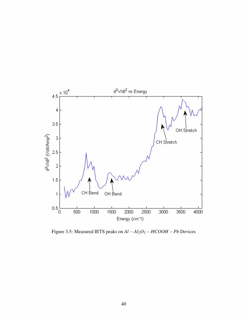
Figure 3.5: Measured IETS peaks on Al−Al2O3−HCOOH−Pb Devices
40
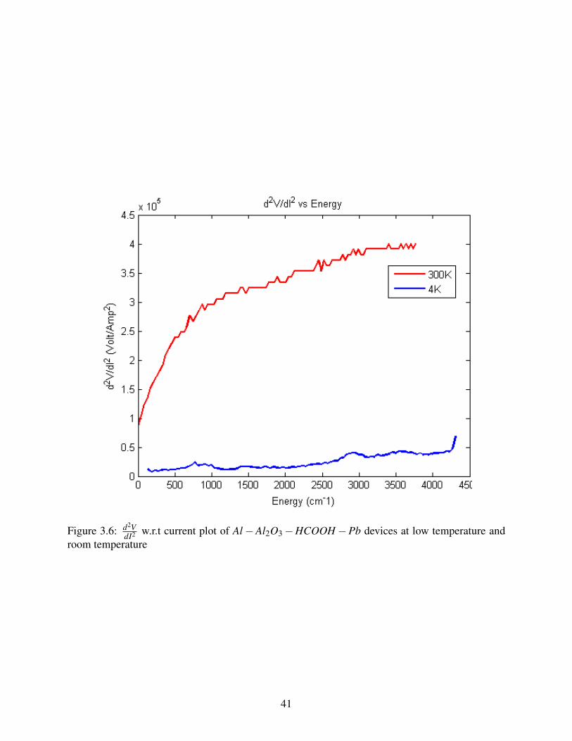
Figure 3.6: d2VdI2 w.r.t current plot of Al−Al2O3−HCOOH−Pb devices at low temperature and
room temperature
41

42
Chapter 4
Thermal Broadening of IETS Peaks
One major limitation of application of inelastic electron tunneling spectroscopy as an e-nose is
that it should be performed at very low temperature typically ∼ 4.7K. At room temperature, due
to thermal smearing of the electrons in metals, broad line-width of IETS peaks are observed. This
phenomena is called “thermal broadening of IETS peaks”. To understand this, one has to com-
pare the band diagram of metal− insulator−metal device at cryogenic temperature and at room
temperature. Metals have continues distribution of electron energy density of states given by
ρ(E) =4π(2m)(3/2)
h3
√E
The conduction electron population for a metal is given by multiplying the density of conduc-
tion electron states ρ(E) times the Fermi function f (E). The number of conduction electrons per
unit volume per unit energy is
dndE
=4π(2m)(3/2)
h3
√E
1e(E−EF )/kT −1
At T = 0 , the Fermi function is a step function and electrons only occupy energy levels up-to
Fermi level. At room temperate, electrons have energy kT ∼ 25mV and occupy energy levels above
the Fermi level. Figure 4.1
43
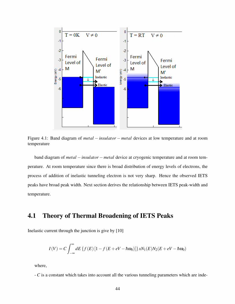
Figure 4.1: Band diagram of metal− insulator−metal devices at low temperature and at roomtemperature
band diagram of metal− insulator−metal device at cryogenic temperature and at room tem-
perature. At room temperature since there is broad distribution of energy levels of electrons, the
process of addition of inelastic tunneling electron is not very sharp. Hence the observed IETS
peaks have broad peak width. Next section derives the relationship between IETS peak-width and
temperature.
4.1 Theory of Thermal Broadening of IETS Peaks
Inelastic current through the junction is give by [10]
I (V ) =Cˆ
∞
−∞
dE f (E) [1− f (E + eV − hω0)]xN1(E)N2(E + eV − hω0)
where,
- C is a constant which takes into account all the various tunneling parameters which are inde-
44

pendent of E and T
- f(E) is the Fermi function for metals
- N1(E) and N2(E) are effective tunneling density of states
- V is applied bias voltage
- hω0 is vibrational energy of the molecule
Since, N1(E) and N2(E) which are effective tunneling density of states are equal to unity for
normal metal and f (E) = 11+eE/kT , above equation will reduce to
I(V ) =Cˆ
∞
−∞
dE(
11+ eE/kT
)(1− 1
1+ e[E+e(V−V0)]/kT
)
Solving above equation we get,
I(V ) =Ce(V −V0)ee(V−V0)/kT
ee(V−V0)/kT −1
differentiating above equation w.r.t V twice we get
d2IdV 2 =C
e2
kT
[ev (v−2)ev +(v+2)
(ev−1)3
]
where v = e(V−V0)kT . Above equation gives d2I
dV 2 as a function of (V −V0). Plotting d2IdV 2 w.r.t
(V −V0), FWHM is give by 5.4kT . If W0 is the actual peak width at T = 0 than
W (T ) =√
(5.4kT )2 +W 20
Next section discuss the experimental results on thermal broadening of IETS peaks in Al−
Al2O3−HCOOH−Pb devices.
45
4.1.1 IETS Peak-width at Various Temperature
Thermal broadening of IETS peaks are empirically measured to estimate the order of electron
energy filtering is required. A <model number> temperature controller is attached to the cryostat
to change the temperature to desired value. PID parameters in temperature controllers is set so
that the temperature is stable up-to 100mK. The device is first brought to desired temperature and
then IETS measurement is performed. To obtain usable second derivative at high temperature,
modulation voltage of 10mV is used.
Figure 4.2 and figure 4.3 shows inelastic electron tunneling spectra of Al−Al2O3−HCOOH−
Pb device at T = 4.2K, T = 10K, T = 30K, and T = 77K respectively. As the temperature at which
the sample is increased, the lines broaden and the peak height decreases. For −CH stretch, at4.2K
the line-width is about 19.8mV , but at 77’K the line-width is about46.2mV . At room temperature
the broadening is too great to get any reasonable estimate of line-width. It must be noted that the
peak width also depends upon the modulation voltage bias used, actual impedance of the device
and if one of the metal is super conducting.
To study the variation of peak width w.r.t temperature two IETS peaks corresponding to −OH
bend and −CH stretch is used. Table 4.1 tabulates peak-width of peak observed for −OH bend
Temperature Peak-width of−OH band (mV ) Peak-width for−CH stretch (mV )4.2K 14.8 19.810K 15 20.230K 16.6 24.177K - 46.2
Table 4.1: IETS peak-width w.r.t. temperature
and −CH stretch at various temperature. Figure 4.4 shows the variation of IETS peak width for
−CH stretch with temperature. Fitting function
W (T ) =√
(5.4kT )2 +W 20
is used to best-fit the data in order to determine absolute peak width W0. The calculated value of
46
W0 is found to be 19.4mV .
Similarly, for −OH bend peak, variation of peak width with respect to temperature is shown
in figure 4.5 . After best fitting the curve the value of absolute peak is found to be W0 = 14.5mV .
This peak simply disappeared at 77K and hence only three points are used for curve fitting. When
temperature of sample is increased, this results in broadening of IETS peaks. At a certain tem-
perature, the peaks are so broad that, different vibrational energy modes of molecules under study
can not be resolved. Next section determine this maximum characteristic temperature and energy
distribution of electrons associated with this temperature.
4.2 Maximum Temperature to Resolve IETS peaks
In order to resolve IETS peaks, the peak-width (FWHM) should be at least of the order of distance
between two consecutive peaks. As shown in table 3.1, the difference in energy of−OH and−CH
bend is of the order of ∼ 50mV . Hence in order to distinguish between these two peaks, the
peak-width should at least be of the order of ∼ 50mV . From figure 4.4 we know, in order to get
peak width of 50mV the experiment should be performed at a temperature not higher than 77K.
Hence the maximum temperature at which HCOOH peak can be observed is Tmax ∼ 77K. (It must
be noted that the value of Tmax depends upon the molecule under study. For some molecule if the
difference between individual vibrational energy level is of the order of ∼ 20mV than Tmax will be
around ∼ 10K)
Now for Tmax = 77K, thermal energy of electrons in metals are 6.6meV . In order to perform
IETS spectroscopy at room temperature, the required electron energy filtering should be of the
order of ∼ 6.6meV . Next chapter describes the theoretical study of using quantum dots as electron
energy filters for this application.
47
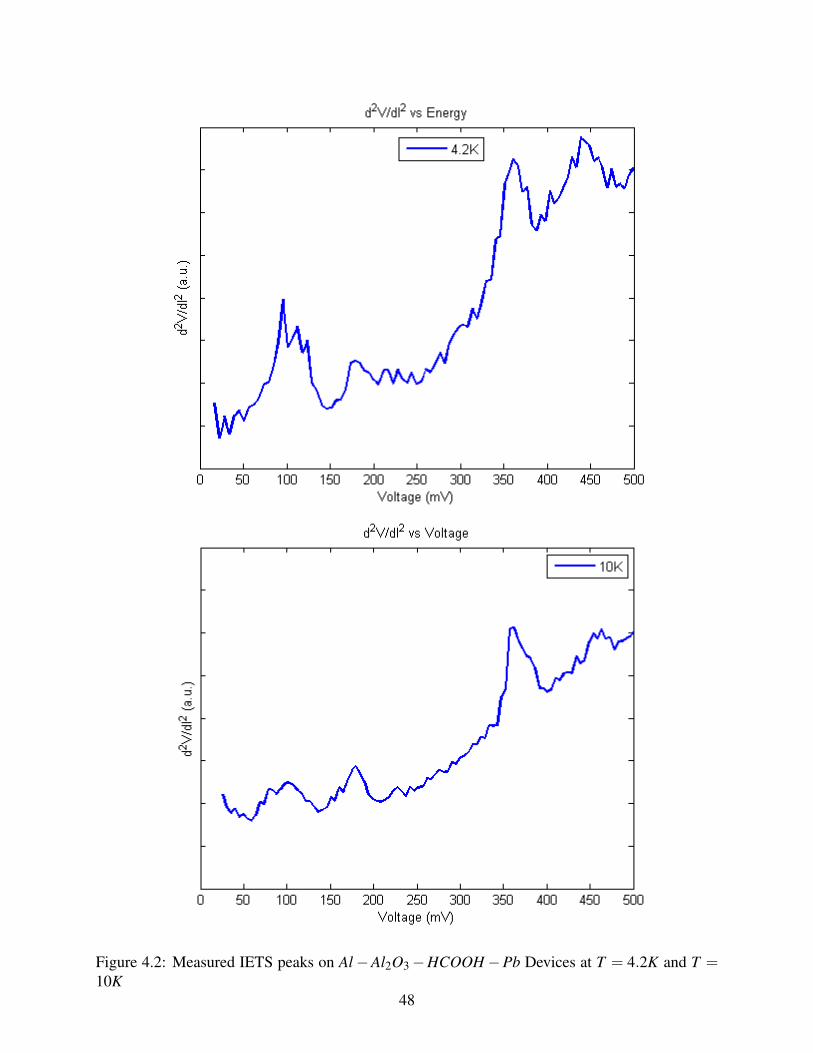
Figure 4.2: Measured IETS peaks on Al−Al2O3−HCOOH−Pb Devices at T = 4.2K and T =10K
48
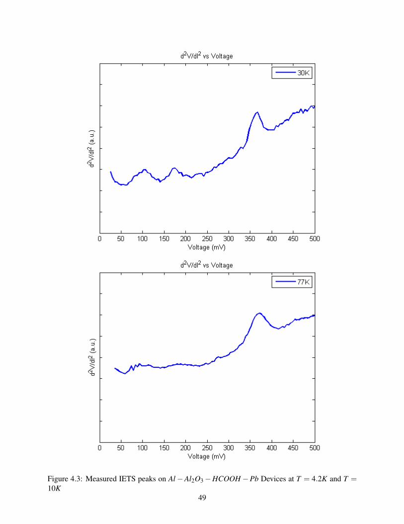
Figure 4.3: Measured IETS peaks on Al−Al2O3−HCOOH−Pb Devices at T = 4.2K and T =10K
49
Figure 4.4: Plot of IETS peak width (W) w.r.t. Temperature for −CH stretch peak
50
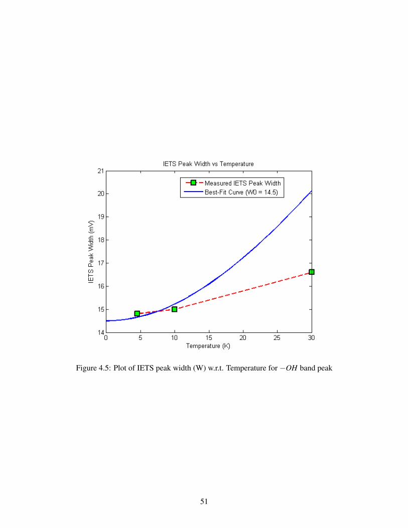
Figure 4.5: Plot of IETS peak width (W) w.r.t. Temperature for −OH band peak
51

52
Chapter 5
Theory of Quantum Dots Electron Energy
Filters
This chapter investigate resonant tunneling through 2-dimentional quantum dot arrays which is
transverse to the direction of tunneling current. This system can be modeled as a potential double
barrier, incorporating a periodic quantum dot structure with the periodicity in the direction perpen-
dicular to the tunneling current. It is assumed that periodic potential is infinitely spread in the plane
of the barrier. The periodic array of quantum dots perpendicular to tunneling current is modeled
as thick quantum well whose δ − f unction is modulated periodically in transverse direction[11].
Thus the potential profile of this system can be written as
U (x,y) =−V0δ (x) f (y)
where, f (y) > 0 is a periodic potential in transverse direction. Assuming that the modulation
function f (y) is week, using the adiabatic approximation the wave function can be written as:
Φ(x,y) = η (y)Ψy (x)
The Schrodinger equation can be then written as:
53
− h2m
∂ 2
∂x2 Ψy (x)−V0δ (x) f (y)Ψy (x) = E (y)Ψy (x)
The solution of above equation is eigenfunction Ψy (x)
Ψy (x) =√
κ0exp(−κ0 [x])
where, κ0 =V0 f (y)m
h2 and eigen energy state
E0 =−mV 2
0 f 2 (y)2h2
The system can be considered as a resonant tunneling diode (figure5.1 ) with mini band width
44 and energy ε1k = E0 +4(2− coskgb− coskzb), where b is the period of quantum dots and
E0 is the energy difference between the Fermi-level of metal and first mini-band in quantum dot
arrays. The energy band due to transverse energy is given by ε2k = E0+U +41 (coskyb+ coskzb),
where U −241 is the gap between the two minibands. In Aluminum and Lead electrodes, energy
of electrons are give by
EAl =h2k2
2mAl
EPb =h2k2
2mPb
where mAland mPbis effective electron mass in aluminum and lead respectively
The current through this double barrier resonant tunneling system consist of both elastic and
inelastic tunneling current. These are discussed next
54

5.1 Current-Voltage Characteristics of QDs Array
The current through the 2-dimentional array of QDs sandwiched between two metal electrodes
consist of both elastic tunneling electrons and inelastic tunneling electrons.
5.2 Elastic Tunneling Through QDs Arrays
The electron Hamiltonian for elastic resonant tunneling is give by[8]
H = ∑ik
εikc†ikcik +∑
k
(εkLc†
kLckL + εkRc†
kRckR
)+∑
k
[VikL
(c†
kLcik + c†ikckL
)+VikR
(c†
kRcik + c†ikckR
)]
where,
1. εik is i− th miniband energy of i− th resonant state in double barrier quantum dot arrays.
2. cik, ckL and ckR are creation operators of electrons in the quantum well ith resonant state with
i− th miniband energy εik for left and right electrode
3. c†ik, c†
kL and c†kR are annihilation operators of electrons in the quantum well ith resonant state
with i− th miniband energy εik for left and right electrode
4. VikL and VikRare the matrix element of elastic tunneling from left and right electrodes to the
i− th miniband state in the quantum well respectively.
It is assumed that the coupling of electrons in metals to quantum well energy level is by elastic
process only. The elastic hopping matrix elements VkAl(Pb)determines the elastic coupling of the
electrons in the aluminum and lead to electrons in quantum dot energy level εkAl(Pb). The coupling
of metals to quantum well ΓAl(Pb) can be determined by these matrix elements using the following
formula:
ΓAl = 2π|VAl|2ρAl
55
on tunneling spectroscopy at room temperature to resolve vibrational energy level of molecules,
thermal energy distribution of electrons should be less than 4E ∼ 6.63mV . The designed quan-
tum dots electron energy filters can only narrow down thermal distribution of electron down to
only4E2dQDs ∼ 10mV . Hence, even though quantum dot electron energy filters can narrow down
thermal distribution of electrons from ∼ 25mV down to ∼ 10mV , its not enough to perform high
resolution inelastic electron tunneling spectroscopy at room temperature. Also, quantum dot en-
ergy filters suffer from charge trapping, which degrades there performance with repeated current-
voltage measurement.
ΓPb = 2π|VPb|2ρPb
where, ρAl = ∑k δ(ε− εkAl
)and ρPb = ∑k δ
(ε− εkPb
)are the densities of states in aluminum and
lead respectively. Since the bandwidth miniband in quantum well is much smaller than the band-
width of energy level in aluminum and lead, one can approximate that the density of states ρAl and
ρPb are constant at in resonant region.
5.3 Inelastic Tunneling Through QDs Array
For the electrons localized in quantum dots well, electron-phonon interaction Hamiltonian is given
by[9]
Hint = ∑q
Mq
(aq +a†
q
)∑k
c†k+qck
where aqand a†q are phonon creation and annihilation operators respectively.
Assuming Einstein phonon with energy hω0 at low temperature, we can write electron-phonon
coupling constant g as:
56
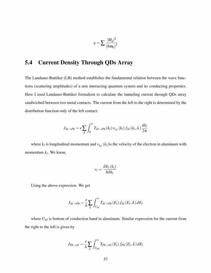
g = ∑|Mq|2
(hω0)2
5.4 Current Density Through QDs Array
The Landauer-Buttiker (LB) method establishes the fundamental relation between the wave func-
tions (scattering amplitudes) of a non interacting quantum system and its conducting properties.
Here I used Landauer-Buttiker formalism to calculate the tunneling current through QDs array
sandwiched between two metal contacts. The current from the left to the right is determined by the
distribution function only of the left contact:
JAl→Pb = e∑λ
ˆ∞
0TAl→Pb (kl)vlAl (kl) fAl (kl,λ )
dkl
2π
where kl is longitudinal momentum and vlAl (kl)is the velocity of the electron in aluminum with
momentum kl . We know,
vl =∂El (kl)
h∂kl
Using the above expression. We get
JAl→Pb =eh ∑
λ
ˆ∞
UAl
TAl→Pb (El) fAl (El,λ )dEl
where UAl is bottom of conduction band in aluminum. Similar expression for the current from
the right to the left is given by
JPb→Al =eh ∑
λ
ˆ∞
UPb
TPb→Al (El) fPb (El,λ )dEl
57
The final expression for current density at a voltage bias V is give by
J (V ) =eh
ˆ∞
−∞
T (E) [FAl (E)−FPb (E)]dE
Where FAl and FPb is Fermi energy distribution of electrons in aluminum and lead respectively.
And the transmission probability T (E) for QDs array.
When a bias is applied across the barrier, the voltage drop is equally distributed between the
two barriers. Taking into account the energy shift in a Fermi distribution function due to bias
voltage, one obtains:
J (V ) =eh
ˆ∞
−∞
T (E) [FAl (E + eV )−FPb (E)]dE
For a 3D tunneling system, above equation can be written as[9]:
J(V ) =eh
ˆ∞
0T (k).dkl
ˆd2ktvl [ fAl (εk)− fPb (εk)]
Since at lower energies T (E) = 0, Integration over E should be actually performed from the
maximum of two conduction band bottoms.
58
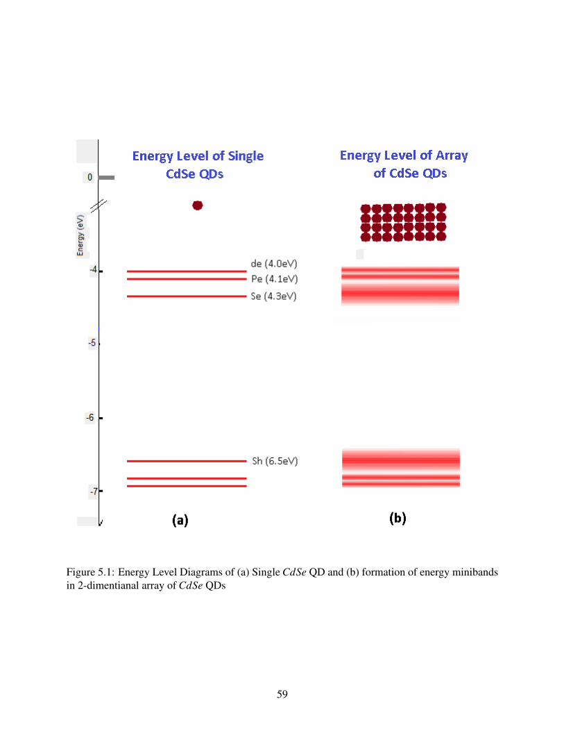
Figure 5.1: Energy Level Diagrams of (a) Single CdSe QD and (b) formation of energy minibandsin 2-dimentianal array of CdSe QDs
59

60
Chapter 6
Fabrication of CdSe QDs Electron Energy
Filters
6.1 Introduction
As described earlier, the reason of the thermal broadening of IETS peak is due to thermal distribu-
tion of electrons in metal. The discrete energy levels in quantum dots can be used to narrow down
the thermal distribution of electrons. This chapter describes the fabrication of electron energy filter
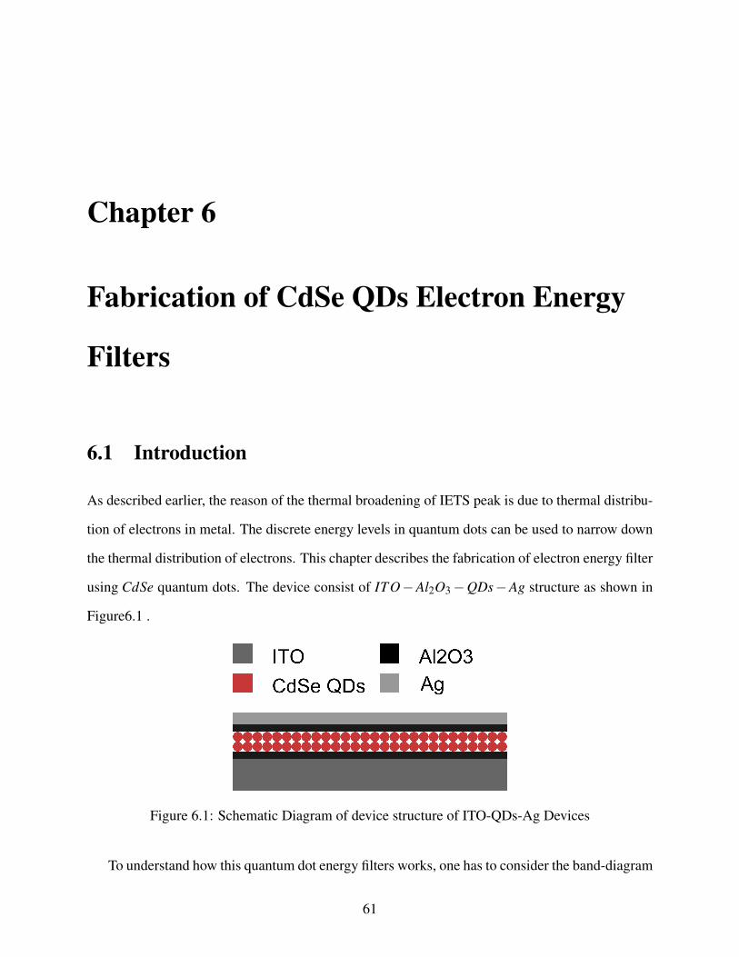
using CdSe quantum dots. The device consist of ITO−Al2O3−QDs−Ag structure as shown in
Figure6.1 .
Figure 6.1: Schematic Diagram of device structure of ITO-QDs-Ag Devices
To understand how this quantum dot energy filters works, one has to consider the band-diagram
61
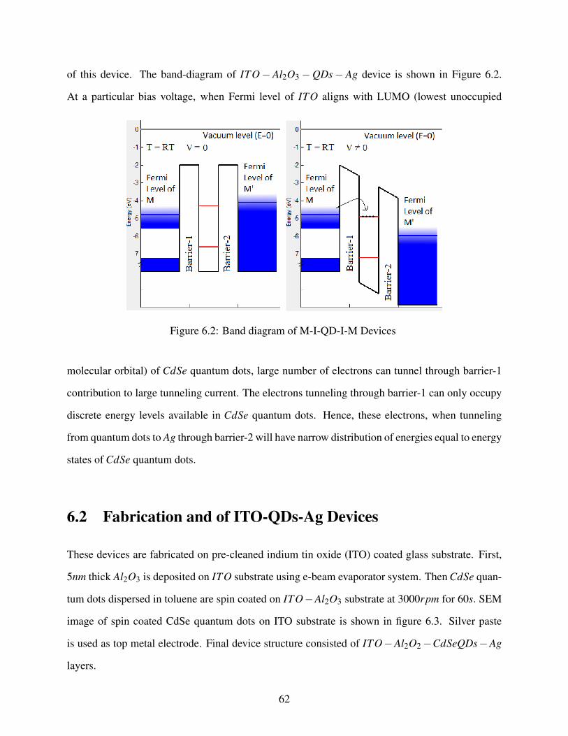
of this device. The band-diagram of ITO−Al2O3−QDs−Ag device is shown in Figure 6.2.
At a particular bias voltage, when Fermi level of ITO aligns with LUMO (lowest unoccupied
Figure 6.2: Band diagram of M-I-QD-I-M Devices
molecular orbital) of CdSe quantum dots, large number of electrons can tunnel through barrier-1
contribution to large tunneling current. The electrons tunneling through barrier-1 can only occupy
discrete energy levels available in CdSe quantum dots. Hence, these electrons, when tunneling
from quantum dots to Ag through barrier-2 will have narrow distribution of energies equal to energy
states of CdSe quantum dots.
6.2 Fabrication and of ITO-QDs-Ag Devices
These devices are fabricated on pre-cleaned indium tin oxide (ITO) coated glass substrate. First,
5nm thick Al2O3 is deposited on ITO substrate using e-beam evaporator system. Then CdSe quan-
tum dots dispersed in toluene are spin coated on ITO−Al2O3 substrate at 3000rpm for 60s. SEM
image of spin coated CdSe quantum dots on ITO substrate is shown in figure 6.3. Silver paste
is used as top metal electrode. Final device structure consisted of ITO−Al2O2−CdSeQDs−Ag
layers.
62
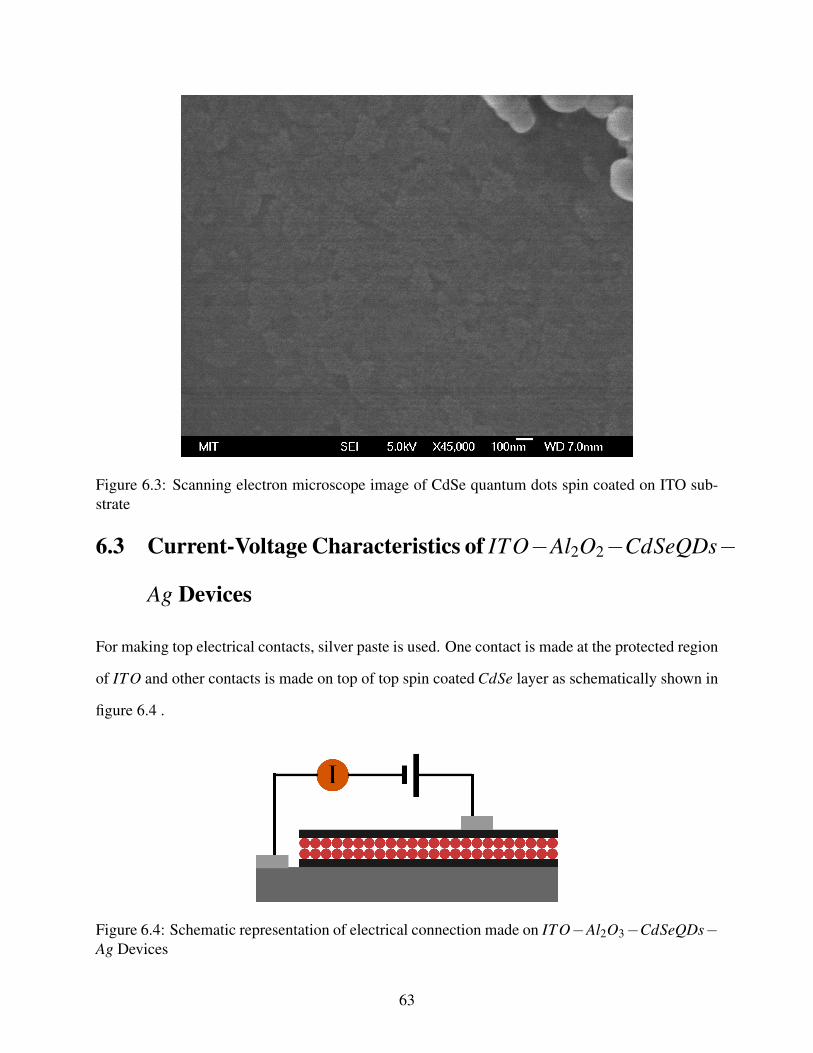
Figure 6.3: Scanning electron microscope image of CdSe quantum dots spin coated on ITO sub-strate
6.3 Current-Voltage Characteristics of ITO−Al2O2−CdSeQDs−
Ag Devices
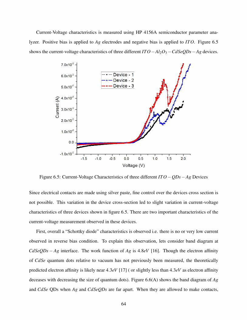
For making top electrical contacts, silver paste is used. One contact is made at the protected region
of ITO and other contacts is made on top of top spin coated CdSe layer as schematically shown in
figure 6.4 .
Figure 6.4: Schematic representation of electrical connection made on ITO−Al2O3−CdSeQDs−Ag Devices
63
Current-Voltage characteristics is measured using HP 4156A semiconductor parameter ana-
lyzer. Positive bias is applied to Ag electrodes and negative bias is applied to ITO. Figure 6.5
shows the current-voltage characteristics of three different ITO−Al2O3−CdSeQDs−Ag devices.
Figure 6.5: Current-Voltage Characteristics of three different ITO−QDs−Ag Devices
Since electrical contacts are made using silver paste, fine control over the devices cross section is
not possible. This variation in the device cross-section led to slight variation in current-voltage
characteristics of three devices shown in figure 6.5. There are two important characteristics of the
current-voltage measurement observed in these devices.
First, overall a “Schottky diode” characteristics is observed i.e. there is no or very low current
observed in reverse bias condition. To explain this observation, lets consider band diagram at
CdSeQDs−Ag interface. The work function of Ag is 4.8eV [16]. Though the electron affinity
of CdSe quantum dots relative to vacuum has not previously been measured, the theoretically
predicted electron affinity is likely near 4.3eV [17] ( or slightly less than 4.3eV as electron affinity
deceases with decreasing the size of quantum dots). Figure 6.6(A) shows the band diagram of Ag
and CdSe QDs when Ag and CdSeQDs are far apart. When they are allowed to make contacts,
64
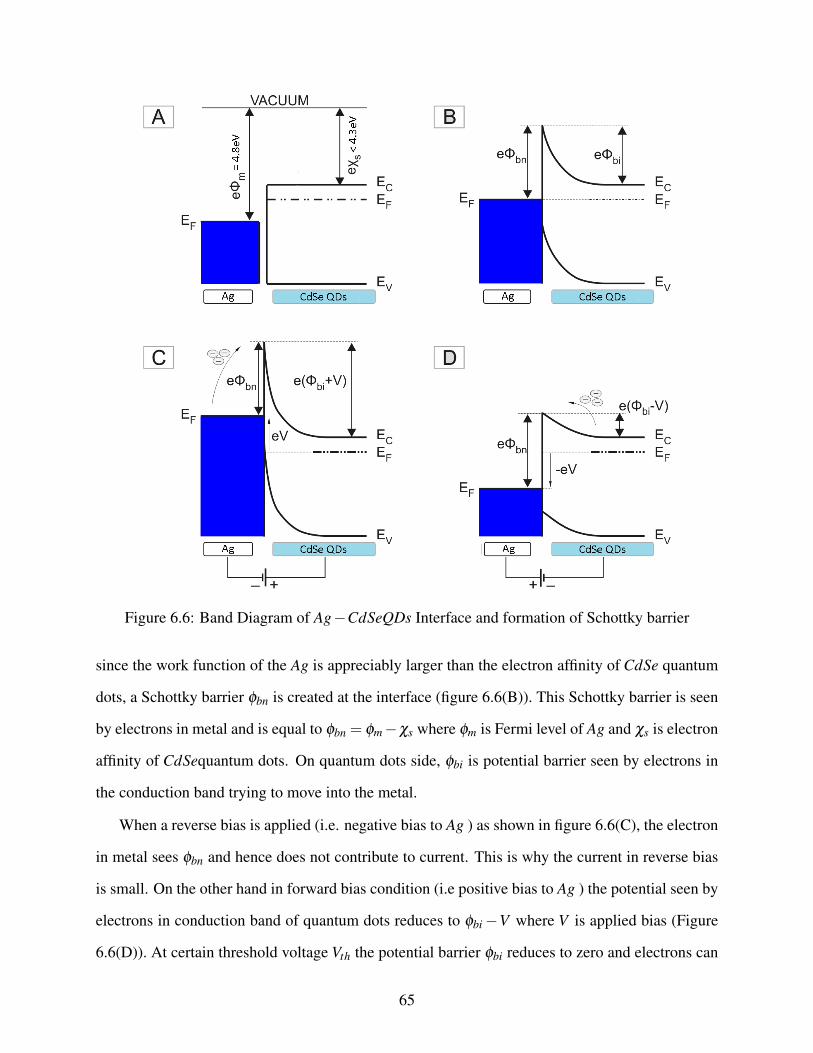
Figure 6.6: Band Diagram of Ag−CdSeQDs Interface and formation of Schottky barrier
since the work function of the Ag is appreciably larger than the electron affinity of CdSe quantum
dots, a Schottky barrier φbn is created at the interface (figure 6.6(B)). This Schottky barrier is seen
by electrons in metal and is equal to φbn = φm−χs where φm is Fermi level of Ag and χs is electron
affinity of CdSequantum dots. On quantum dots side, φbi is potential barrier seen by electrons in
the conduction band trying to move into the metal.
When a reverse bias is applied (i.e. negative bias to Ag ) as shown in figure 6.6(C), the electron
in metal sees φbn and hence does not contribute to current. This is why the current in reverse bias
is small. On the other hand in forward bias condition (i.e positive bias to Ag ) the potential seen by
electrons in conduction band of quantum dots reduces to φbi−V where V is applied bias (Figure
6.6(D)). At certain threshold voltage Vth the potential barrier φbi reduces to zero and electrons can
65
contribute to current. For ITO−Al2O3−CdSeQDs−Ag devices the value of threshold voltage is
found to be Vth ∼ 0.25V .
Another interesting characteristics of current-voltage measurement is observation of negative
differential resistance. To understand this interesting behavior, lets consider the band diagram of
ITO−QDs interface as shown in figure 6.7. The work-function of Indium tin oxide (ITO) is
Figure 6.7: Band diagram of ITO-QDs interface
4.77eV [14, 15]. However, there is an important difference between ITO and a metal electrode:
ITO consists of Sn-doped (n-doped) In2O3, an intrinsic insulator. Even as an n-doped conductor,
ITO still has a wide band gap from3.50eV to 4.06eV [12, 13]. Based on how ITO is grown (% of
O2 in growth environment) the Fermi level is either in conduction band or slightly above (∼ 0.7eV )
the conduction band [18][14].
The observation of negative differential resistance in current-voltage characteristics of ITO−
Al2O3(5nm)−CdSeQDs( 80nm)− Ag can be explained using the theoretical model developed
66
for arrays of quantum dots sandwiched between two metal electrodes. As described in chapter
5, 2D array of quantum dots can be modeled as resonant tunneling diode with several minibands
having finite mini-bandwidth. Figure 6.8 shows the simplified band diagram of ITO−Al2O3−
Figure 6.8: Band diagram of theITO−Al2O3(5nm)−CdSeQDs( 80nm)−Al2O3(5nm)−Ag De-vices
CdSeQDs−Ag devices modeled as double barrier resonant tunneling diode. Initially at low bias
condition, when Fermi level of ITO is below the first energy state of CdSe quantum dots, no
electron tunneling is possible as there is no energy state available to be occupied by tunneling
electron. Since there is no electron tunneling, very low current is observed at this bias voltage.
As the bias voltage is gradually increased, at around ∼ 0.25V , Fermi level of ITO aligns with
the first energy miniband of CdSeQDs as shown in figure 6.8(b). At this bias, large electrons can
tunnel and occupy the energy state of quantum dots resulting in sudden increase in current (figure
6.5). When the bias voltage is further increased, the first energy state of quantum dots now aligns
with the bandgap of ITO.As there are now electron available in the bandgap of ITO to contribute
to tunneling current, the total current will again decrease (figure 6.5). This led to observation of
negative differential resistance in ITO−Al2O3−CdSeQDs−Ag devices.
The peak-width of peak observed in IV measurement is ∼ 1V , as shown in figure 6.8, this
peak is observed due to electron tunneling from conduction band in ITO to miniband of array of
quantum dot structure. The width of conduction band in ITO is ∼ 0.7mV [18][14] and varies with
% of oxygen present in ITO. Given that width of conduction band in ITO is not precisely known,
67
its difficult to predict the width of minibands formed in CdSe quantum dots array.
These devices have some technological limitation in terms of device fabrication. These limita-
tions are as follows -
1. For tunneling barrier, Al2O3 layer is deposited using e-beam evaporator. Such deposited thin
film usually have some pin holes and can contribute to leakage current which is much higher
than tunneling current.
2. Since the top electrical contacts are made using Ag conducting paste, there is a difficulty in
keeping the same device cross-section all across the various fabricated devices.
3. The band diagram of ITO is not precisely known, hence the width of minibands in 2-
dimentional array of quantum dots can not be derived from IV characteristics of these de-
vices.
To overcome these problems, new sets of devices are fabricated were aluminum is used as one
electrode. On top of aluminum an oxide layer is grown using Rf oxygen plasma oxidation tech-
nique. The grown aluminum oxide acts as tunneling barrier. For top electrode Pb is used. The
final device structure consist of Al−Al2O3−QDs−Pb system. Fabrication of these devices are
discussed in next section.
6.4 Fabrication of Al−Al2O3−QDs−Pb Tunneling Device
The device fabrication process consist of following steps
1. 1mm wide, 10mm long and 100nm thick aluminum electrode is deposited on pre-cleaned
glass substrate using thermal vapor deposition system.
2. Aluminum oxide is grown on top of Al using Rf plasma oxidation process. Oxide growth is
carried out for 10s at Rf power of 10W and oxygen flow rate of 1sccm.
68
3. 480nm CdSe quantum dots dispersed in toluene are spin coated on top of aluminum oxide
at 3000rpm for 60s. For comparison purpose another device is fabricated without quantum
dots.
4. For top metal electrode various metals such as Ag, Au, Al and Pb are deposited using thermal
vapor deposition system.
Table 6.1 tabulates resistance and capacitance of some Al−Al2O3−QDs−M′
devices, where,
Device Structure Resistance CapacitanceAl-Al2O3-Pb 0.8K 34nF
Al-Al2O3-QDs-Pb ~7M 4.5nFAl-Al2O3-QDs-Au ~10 -
Al-QDs (480nm)-Al, 3000rpm ~3M 4nFAl-Al2O3-QDs-Ag ~4 -
Table 6.1: Resistance and Capacitance of M− I−QDs−M Devices
M′
is Pb, Au, Ag, and Al. It can be seen in table 6.1 that the resistance of devices with Au and
Ag as top electrode is very small. This is due to the fact that these metals have small atomic
size and high kinetic energy at room temperature. During the thermal vapor deposition of these
metals, they tend to diffuse through the QDs layer resulting in very small device resistance. On the
other hand Pb has large atomic size and low kinetic energy at room temperature and hence can not
diffuse through CdSe QDs layer. For this reason final current-voltage measurement is performed
on Al−AL2O3−CdSeQDs−Pb devices.
6.5 Current-Voltage Characteristics of Al−Al2O3−QDs−Pb
Devices
Indium soldering is used to make electrical contact with Al and Pb leads. Current-voltage mea-
surement is performed using Keithley 6487 picoammeter/voltage source. The common observa-
tion of Al−Al2O3−QDs−Pb devices is that they have very high resistance. Also, the resistance
69
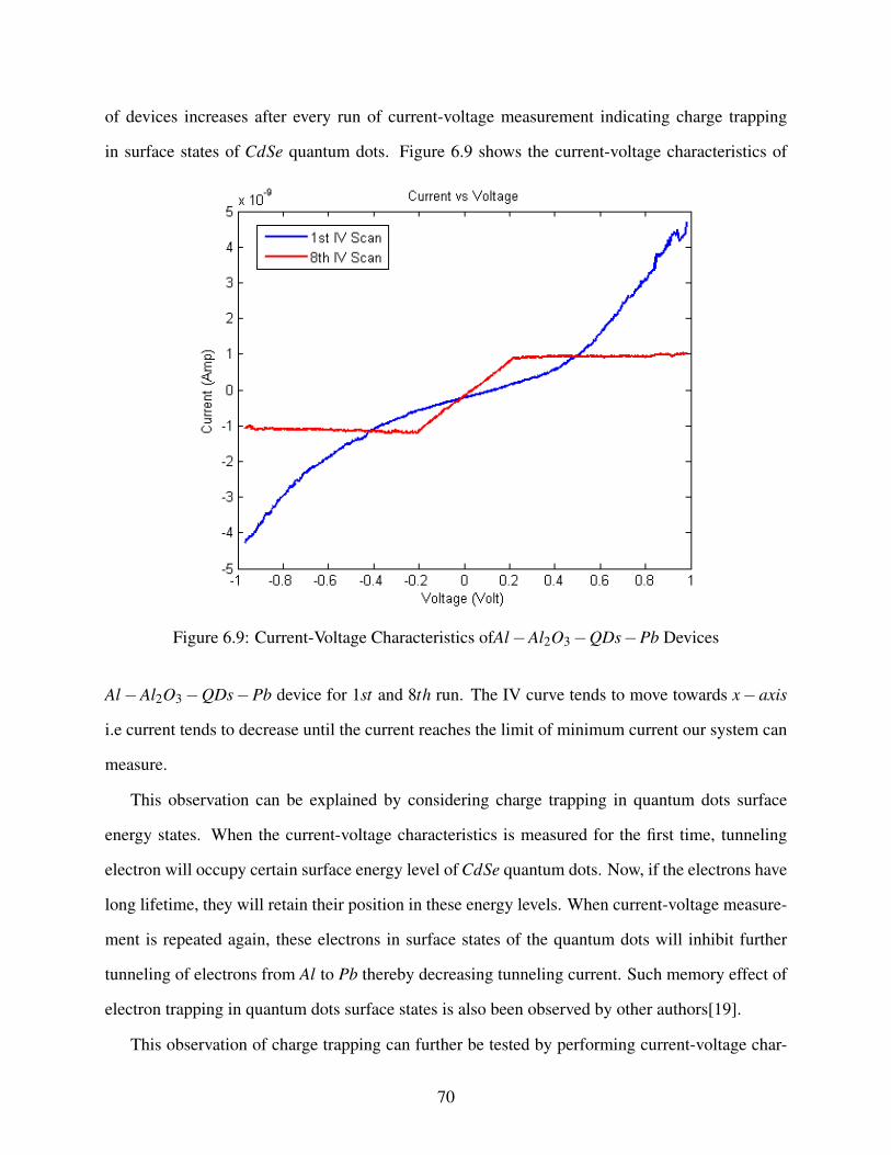
of devices increases after every run of current-voltage measurement indicating charge trapping
in surface states of CdSe quantum dots. Figure 6.9 shows the current-voltage characteristics of
Figure 6.9: Current-Voltage Characteristics ofAl−Al2O3−QDs−Pb Devices
Al−Al2O3−QDs−Pb device for 1st and 8th run. The IV curve tends to move towards x− axis
i.e current tends to decrease until the current reaches the limit of minimum current our system can
measure.
This observation can be explained by considering charge trapping in quantum dots surface
energy states. When the current-voltage characteristics is measured for the first time, tunneling
electron will occupy certain surface energy level of CdSe quantum dots. Now, if the electrons have
long lifetime, they will retain their position in these energy levels. When current-voltage measure-
ment is repeated again, these electrons in surface states of the quantum dots will inhibit further
tunneling of electrons from Al to Pb thereby decreasing tunneling current. Such memory effect of
electron trapping in quantum dots surface states is also been observed by other authors[19].
This observation of charge trapping can further be tested by performing current-voltage char-
70

acteristics at low temperature. First, device is cooled to 4.2K and current-voltage measurement is
performed. The device showed very high resistance with virtually no tunneling current (< 10−12A).
This can be explained by the fact that all the electrons are in valance band and hence will not
contribute to any tunneling current. The device is then brought back to room temperature and a
current-voltage measurement is performed.
Figure 6.10 shows current-voltage measurement of device which was cooled to 4.2K and then
Figure 6.10: Current-Voltage characteristics of Al−Al2O3−QDs−Pb devices which were cooledto 4.2K and then brought to room temperature for measurement
brought back to room temperature for current-voltage measurement. Positive bias is applied to
Pb electrode and voltage is swept from −2V to 2V in steps of 10mV . The zero current gap in
the current-voltage characteristics can be associated with the band gap of CdSe quantum dots.
Current onset for bias occurs when there is resonance between the Fermi energy of Al and the first
quantized conduction energy level of CdSe quantum dots. This led to stairs like characteristics in
current-voltage measurement as shown in figure 6.10.
71
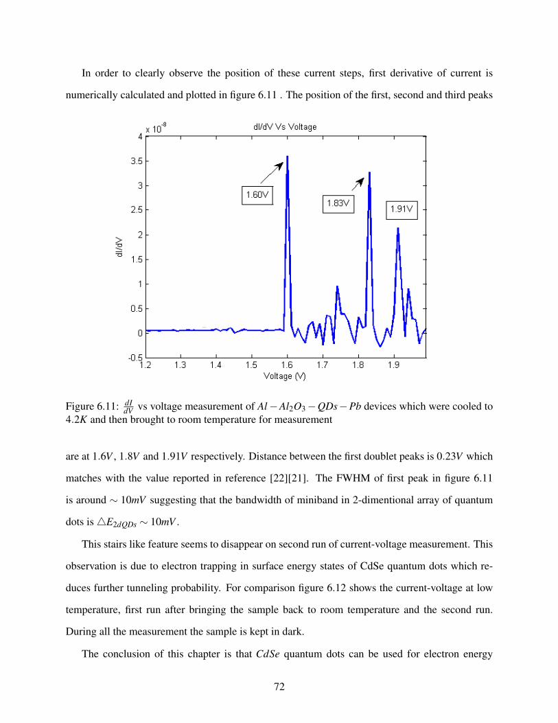
In order to clearly observe the position of these current steps, first derivative of current is
numerically calculated and plotted in figure 6.11 . The position of the first, second and third peaks
Figure 6.11: dIdV vs voltage measurement of Al−Al2O3−QDs−Pb devices which were cooled to
4.2K and then brought to room temperature for measurement
are at 1.6V , 1.8V and 1.91V respectively. Distance between the first doublet peaks is 0.23V which
matches with the value reported in reference [22][21]. The FWHM of first peak in figure 6.11
is around ∼ 10mV suggesting that the bandwidth of miniband in 2-dimentional array of quantum
dots is4E2dQDs ∼ 10mV .
This stairs like feature seems to disappear on second run of current-voltage measurement. This
observation is due to electron trapping in surface energy states of CdSe quantum dots which re-
duces further tunneling probability. For comparison figure 6.12 shows the current-voltage at low
temperature, first run after bringing the sample back to room temperature and the second run.
During all the measurement the sample is kept in dark.
The conclusion of this chapter is that CdSe quantum dots can be used for electron energy
72
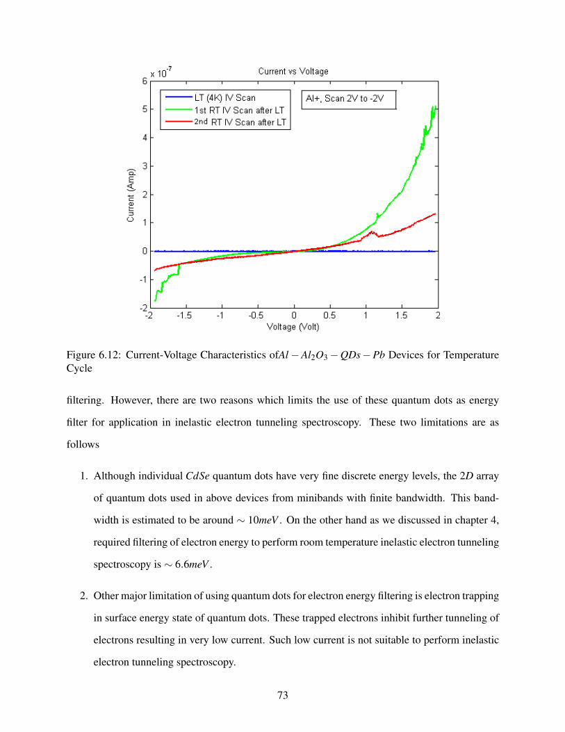
Figure 6.12: Current-Voltage Characteristics ofAl−Al2O3−QDs−Pb Devices for TemperatureCycle
filtering. However, there are two reasons which limits the use of these quantum dots as energy
filter for application in inelastic electron tunneling spectroscopy. These two limitations are as
follows
1. Although individual CdSe quantum dots have very fine discrete energy levels, the 2D array
of quantum dots used in above devices from minibands with finite bandwidth. This band-
width is estimated to be around ∼ 10meV . On the other hand as we discussed in chapter 4,
required filtering of electron energy to perform room temperature inelastic electron tunneling
spectroscopy is ∼ 6.6meV .
2. Other major limitation of using quantum dots for electron energy filtering is electron trapping
in surface energy state of quantum dots. These trapped electrons inhibit further tunneling of
electrons resulting in very low current. Such low current is not suitable to perform inelastic
electron tunneling spectroscopy.
73

To avoid formation of minibands in array of quantum dots, electron transport through single quan-
tum dot is studied.
74
Chapter 7
Electron Transport through Single CdSe
Quantum dot
The device structure discussed in chapter 6, consisted of an array of quantum dots sandwiched
between two metals. In an array of quantum dots, each energy level of quantum dots appear as
miniband which limits the resolution with which electron energy filtering is achievable in such
system. This chapter studies electron transport through single quantum dot. In current system, it is
expected that the current will be observed only through individual energy level of quantum dots as
compared to minibands formed in an array of quantum dots. Current-Sensing atomic force spec-
troscopy (CSAFM) is used to study electron transport through single quantum dot. This chapter
first describes current-sensing atomic force microscopy, followed by current-voltage spectroscopy
of single quantum dot and conclude with presenting measured data.
7.1 Current-Sensing Atomic Force Spectroscopy
In current sensing AFM (CS-AFM) an ultra-sharp AFM cantilever, coated with conducting film,
probes the conductivity and topography of the sample surface. A bias voltage is applied to the
sample while the cantilever is kept at virtual ground. The cantilever probe is connected to a current
pre-amp which converts the measured current into voltage [20]. This voltage is then fed into data
75
acquisition system and used to calculated current. As in contact mode, the tip force is held constant
throughout the scan. Current is used to construct the conductivity image. It is also used for current-
voltage spectroscopy where the cantilever tip is kept at a fixed location and bias voltage is sweep
and current is measured.
7.2 AFM Imaging of CdSe Quantum Dots
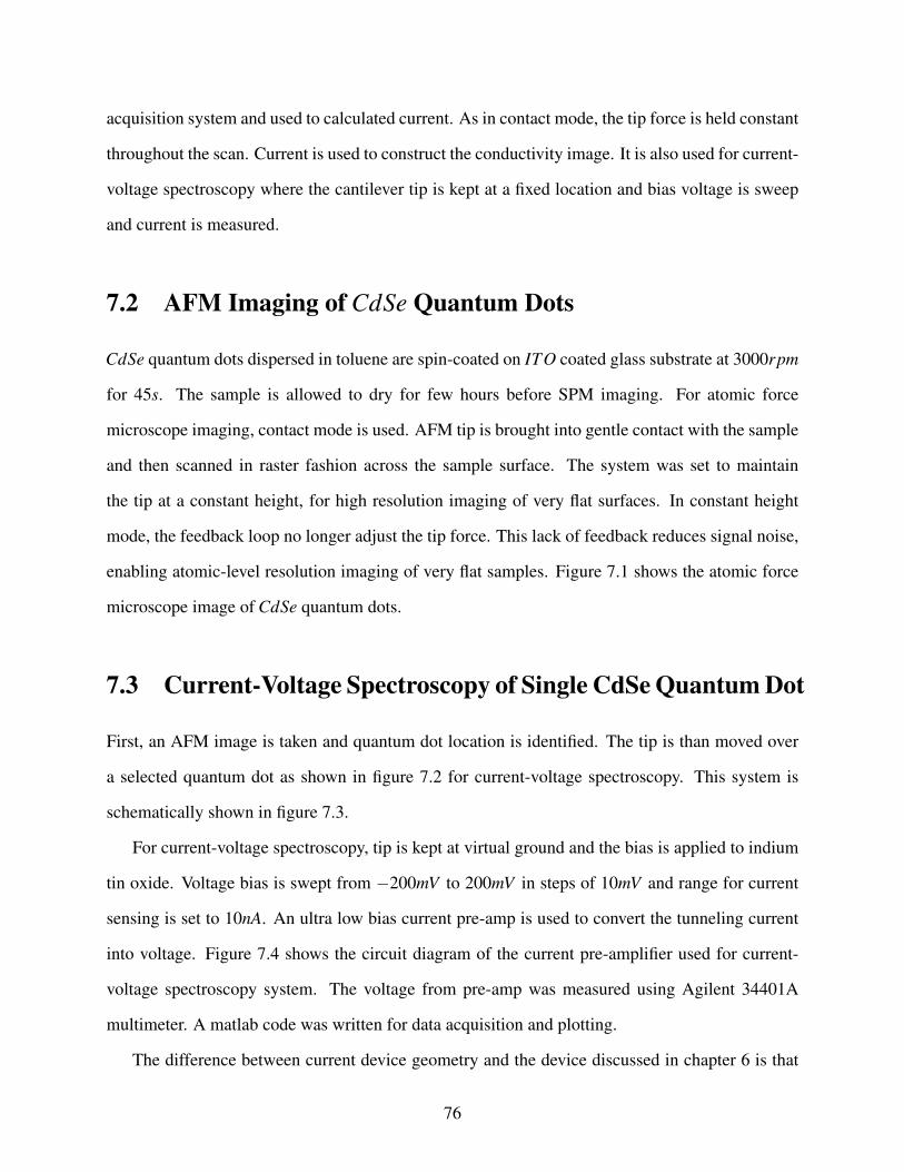
CdSe quantum dots dispersed in toluene are spin-coated on ITO coated glass substrate at 3000rpm
for 45s. The sample is allowed to dry for few hours before SPM imaging. For atomic force
microscope imaging, contact mode is used. AFM tip is brought into gentle contact with the sample
and then scanned in raster fashion across the sample surface. The system was set to maintain
the tip at a constant height, for high resolution imaging of very flat surfaces. In constant height
mode, the feedback loop no longer adjust the tip force. This lack of feedback reduces signal noise,
enabling atomic-level resolution imaging of very flat samples. Figure 7.1 shows the atomic force
microscope image of CdSe quantum dots.
7.3 Current-Voltage Spectroscopy of Single CdSe Quantum Dot
First, an AFM image is taken and quantum dot location is identified. The tip is than moved over
a selected quantum dot as shown in figure 7.2 for current-voltage spectroscopy. This system is
schematically shown in figure 7.3.
For current-voltage spectroscopy, tip is kept at virtual ground and the bias is applied to indium
tin oxide. Voltage bias is swept from −200mV to 200mV in steps of 10mV and range for current
sensing is set to 10nA. An ultra low bias current pre-amp is used to convert the tunneling current
into voltage. Figure 7.4 shows the circuit diagram of the current pre-amplifier used for current-
voltage spectroscopy system. The voltage from pre-amp was measured using Agilent 34401A
multimeter. A matlab code was written for data acquisition and plotting.
The difference between current device geometry and the device discussed in chapter 6 is that
76
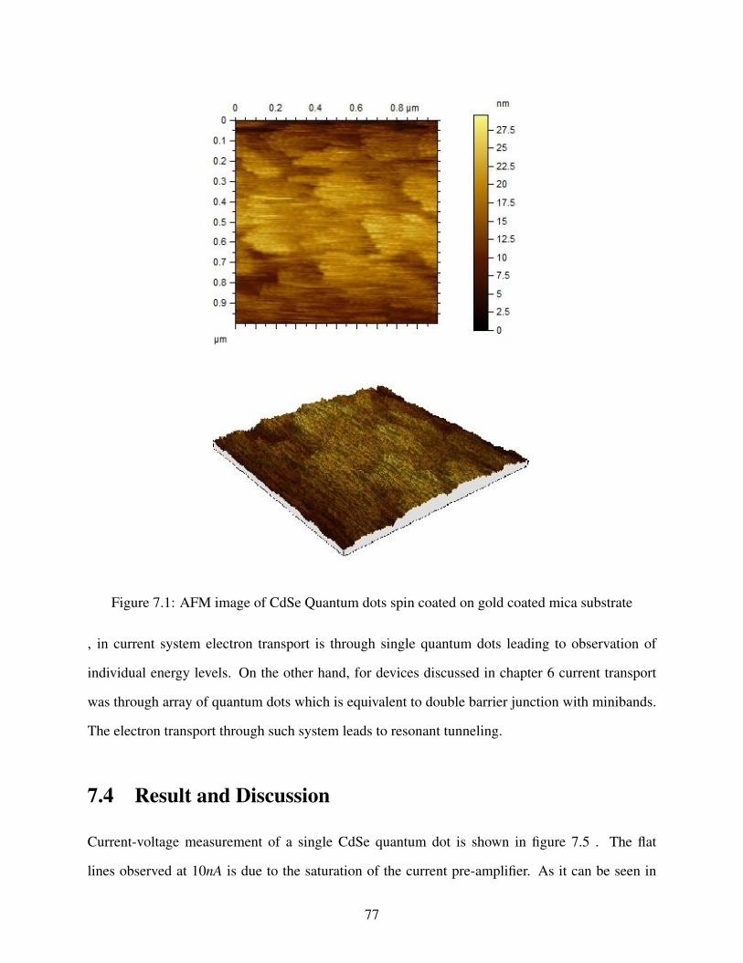
Figure 7.1: AFM image of CdSe Quantum dots spin coated on gold coated mica substrate
, in current system electron transport is through single quantum dots leading to observation of
individual energy levels. On the other hand, for devices discussed in chapter 6 current transport
was through array of quantum dots which is equivalent to double barrier junction with minibands.
The electron transport through such system leads to resonant tunneling.
7.4 Result and Discussion
Current-voltage measurement of a single CdSe quantum dot is shown in figure 7.5 . The flat
lines observed at 10nA is due to the saturation of the current pre-amplifier. As it can be seen in
77
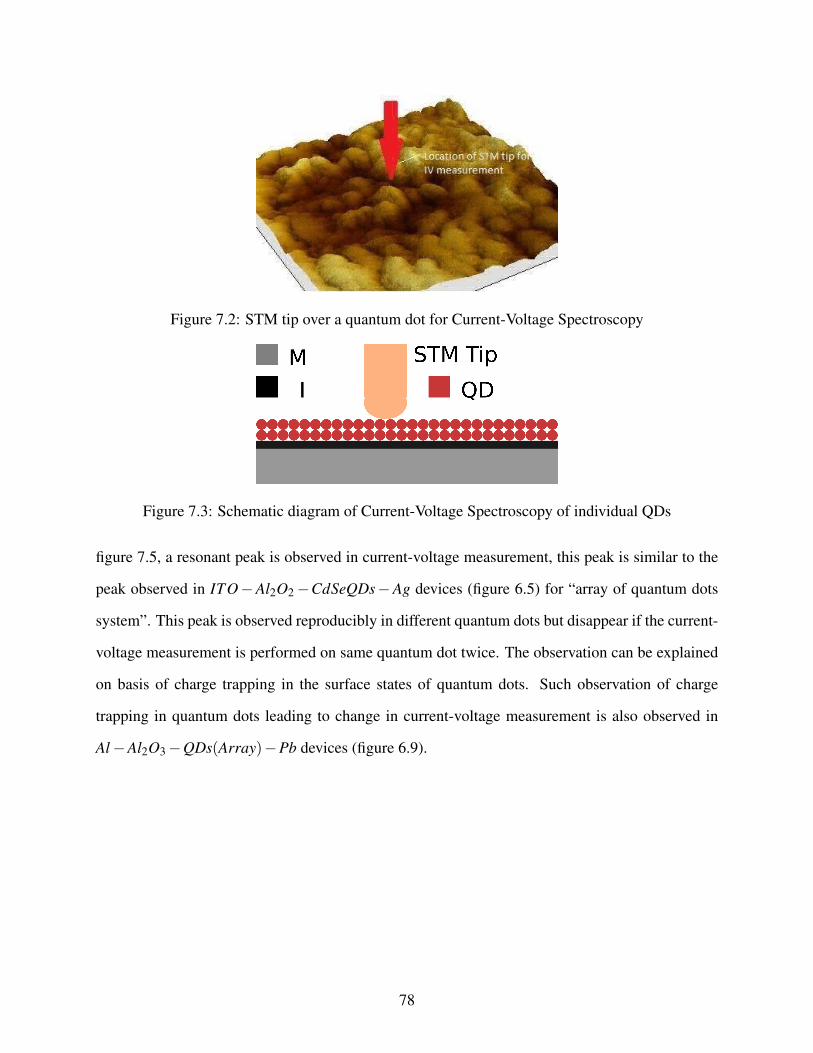
Figure 7.2: STM tip over a quantum dot for Current-Voltage Spectroscopy
Figure 7.3: Schematic diagram of Current-Voltage Spectroscopy of individual QDs
figure 7.5, a resonant peak is observed in current-voltage measurement, this peak is similar to the
peak observed in ITO−Al2O2−CdSeQDs−Ag devices (figure 6.5) for “array of quantum dots
system”. This peak is observed reproducibly in different quantum dots but disappear if the current-
voltage measurement is performed on same quantum dot twice. The observation can be explained
on basis of charge trapping in the surface states of quantum dots. Such observation of charge
trapping in quantum dots leading to change in current-voltage measurement is also observed in
Al−Al2O3−QDs(Array)−Pb devices (figure 6.9).
78
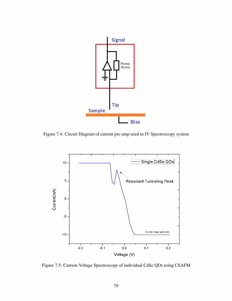
Figure 7.4: Circuit Diagram of current pre-amp used in IV Spectroscopy system
Figure 7.5: Current-Voltage Spectroscopy of individual CdSe QDs using CSAFM
79

80
Chapter 8
Summary and Conclusion
8.1 Summary
To summarize, we started with a problem of performing high resolution inelastic electron tunneling
spectroscopy to resolve molecular vibrations at room temperature. At room temperature, electrons
possess thermal energy kT (∼ 25mV ) and occupy broad range of energy levels available in metals.
This thermal distribution of electrons around Fermi-level limits the resolution of inelastic electron
tunneling spectroscopy.
I proposed to use “electron energy filters” to narrow down thermal distribution of electrons in
order to increase the resolution of inelastic electron tunneling spectroscopy at room temperature.
Before designing such “electron energy filters”, one has to quantitatively determine the specifica-
tion i.e. extent of filtering (or Q-factor) required to perform room temperature inelastic electron
tunneling spectroscopy. This information is derived by studying thermal broadening on IETS peaks
w.r.t temperature. Inelastic tunneling spectra is measured at various temperature to determine max-
imum temperature at which IETS peaks can be resolved. This information is used to derive the
“maximum energy distribution”4E , of electrons which can still give usable IET spectra that can
clearly resolve vibrational modes of molecules.
For HCOOH , vibrational energy modes are separated by approximately∼ 50mV energy. Now,
81
in order to resolve HCOOH energy levels, peak widths in IET spectra should not be more than
∼ 50mV . By studying the variation of IET spectra peak-width w.r.t temperature, we know that
this corresponds to a temperature Tmax ∼ 77K (section 4.4). At this temperature, electrons have
thermal energy distribution of 4E ∼ 6.63mV . Hence, in order to resolve HCOOH peaks at room
temperature, one has to design electron energy filter that can narrow down thermal distribution
of electrons from 4E ∼ 25mV down to 4E ∼ 6.63mV . It must be noted that, this requirements
will change with molecules under study. For example, if for a molecule, the difference between
individual vibrational energy level is of the order of ∼ 20mV than Tmax will be around ∼ 10K and
allowed distribution of energy level will be only4E ∼ 0.8meV .
For designing electron energy filter, I used quantum dots. We know that number of electron in
an energy state E is give by n(E) = ρ(E) f (E). Where, ρ(E) is energy density of state and f (E) is
Fermi function. Now, for metals ρ(E) is a continuous function so every electrons possessing some
thermal energy can occupy available energy states resulting in thermal distribution of electrons.
On the other hand, quantum dots due to there small size have discrete values for density of states
i.e. ρQD(E) is like a delta-function. So even though electrons have broad distribution of thermal
energy at room temperature, they can only occupy certain fixed energy levels available in quantum
dots. In other words, we can narrow down thermal energy distribution of electrons down to the
energy levels available in quantum dots.
Due to the technological limitation of fabricating a device with a single quantum dot, I used a
2−dimensional array of quantum dots as electron energy filter. However, it must be noted that the
density of state function for single quantum dot ρQD(E) is different from the density of state func-
tion for a 2-dimentional array of quantum dots ρ2dQDs(E). The density of state function ρ2dQDs(E)
for 2-dimentional array of quantum dots is calculated by solving the electron wave-function in a
potential consisting of quantum well δ − f unction modulated periodically in transverse direction.
The calculation suggest that unlike individual quantum dots, 2-dimentional array of quantum dots
result in a formation of miniband energy levels with band width of 4E2dQDs = 44 and energy
ε1k = E0 +4(2− coskgb− coskzb)(chapter 5). The bandwidth of minibands in 2-dimentional ar-
82
ray of quantum dots determine the “filtering capability” (or Q-factor) of quantum dots electron
energy filters.
CdSe quantum dots are used for fabrication of energy filters. The device consist of metal−
insulator− 2dQDsArray−metal structure. Two different sets of devices are fabricated with
device structure consisting of ITO−Al2O3−CdSeQDs−Ag and Al−Al2O3−CdSeQDs−Pb
layers. The observation of negative differential resistance (NDR) in current-voltage measure-
ment of ITO− Al2O3 −CdSeQDs− Ag devices (figure 6.5) and stairs like characteristics for
Al−Al2O3−CdSeQDs−Pb devices (figure 6.10) confirms that the electron transport is through
minibands of 2-dimentional quantum dots array. The width 4E2dQDs of first miniband calcu-
lated using current-voltage measurement on Al − Al2O3 −CdSeQDs− Pb device suggest that
4E2dQDs ∼ 10mV (section 6.5). On the other hand, required energy filtering to resolve HCOOH
vibrational peak at room temperature is4E ∼ 6.63mV (section 4.2). Hence, even though electron
energy filtering is possible using quantum dots, its not enough to perform high resolution inelastic
electron tunneling spectroscopy at room temperature.
Another important limitation of using quantum dots for energy filtering is “charge trapping”.
The observation of negative differential resistance (NDR) in current-voltage measurement of ITO−
Al2O3−CdSeQDs−Ag devices and stairs like characteristics in Al−Al2O3−CdSeQDs−Pb de-
vices gradually disappear with repeated scan of current-voltage measurement. The resistance of
the device gradually increases with repeated IV measurement and eventually the device turn into
off-state (i.e. very high impedance) (figure 6.12). This charge trapping in quantum dots is used
as an advantage in quantum dot memory devices, however is a limitation for there application as
electron energy filters.
8.2 Conclusion
Briefly, the conclusion of my thesis is as follows:
In order to perform inelastic electron tunneling spectroscopy at room temperature to resolve
83
vibrational energy level of molecules, thermal energy distribution of electrons should be less than
4E ∼ 6.63mV . The designed quantum dots electron energy filters can only narrow down ther-
mal distribution of electron down to only 4E2dQDs ∼ 10mV . Hence, even though quantum dot
electron energy filters can narrow down thermal distribution of electrons from ∼ 25mV down to
∼ 10mV , its not enough to perform high resolution inelastic electron tunneling spectroscopy at
room temperature. Also, quantum dot energy filters suffer from charge trapping, which degrades
there performance with repeated current-voltage measurement.
8.3 Discussion - Quantum dots vs Odorant Receptors
As we saw in chapter 5, unlike individual quantum dots, a 2-dimentional array of quantum dots
result in a formation of energy minibands. The bandwidth of these minibands determines the
“filtering capability” (or Q-factor) of quantum dots electron energy filters. This work suggest that,
in order to improve the performance of electron energy filters, they should be fabricated using
“single quantum dot” as compare to “array of quantum dots” used in this work.
If biological olfaction is based on IETS[1], doing IETS with odorant receptors proteins ( figure
8.1 ) would involve addition and removal of electrons at well defined energy levels on either side
of an odorant-sized binding site which serves as the tunneling gap. As shown in figure 8.1, the
receptor protein accepts electrons from a soluble electron donor (NADPH). When the receptor
binding site is empty , electrons are unable to tunnel across the binding site because no empty levels
are available at the appropriate energy. When an odorant (here represented as an elastic dipole)
occupies the binding site, electrons can lose energy during tunneling by exciting its vibrational
mode. This only happens if the energy of the vibrational mode equals the energy gap between the
filled and empty levels.
The study of electron transport through single quantum dots done in this work suggests that
the size of the dot should be less than ∼ 2.5nm to be used in room temperature IET spectroscopy.
Interestingly, this length scale is consistent with the size of donor and acceptor sites in odorant
84
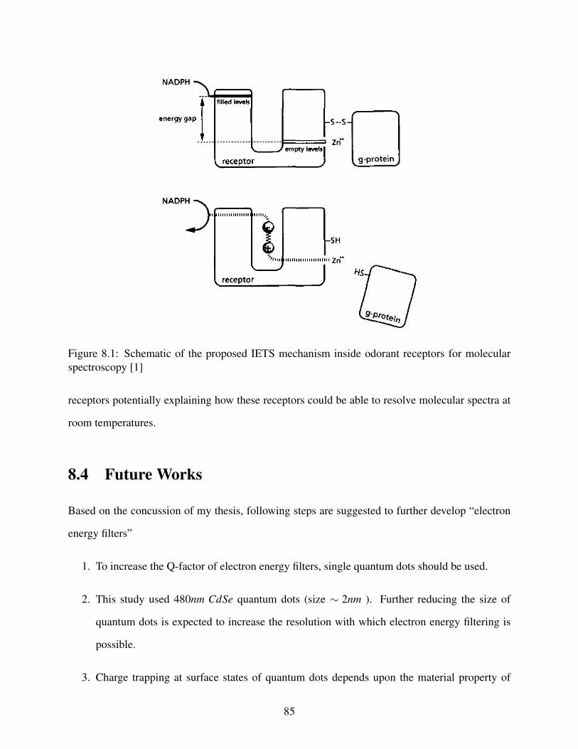
Figure 8.1: Schematic of the proposed IETS mechanism inside odorant receptors for molecularspectroscopy [1]
receptors potentially explaining how these receptors could be able to resolve molecular spectra at
room temperatures.
8.4 Future Works
Based on the concussion of my thesis, following steps are suggested to further develop “electron
energy filters”
1. To increase the Q-factor of electron energy filters, single quantum dots should be used.
2. This study used 480nm CdSe quantum dots (size ∼ 2nm ). Further reducing the size of
quantum dots is expected to increase the resolution with which electron energy filtering is
possible.
3. Charge trapping at surface states of quantum dots depends upon the material property of
85

quantum dots. In order to avoid such charge trapping, another classes of quantum dots such
as PbS, PbSe or graphene quantum dots can be studied.
86

Bibliography
[1] Turin, Chem. Senses, 1996, 21, 773
[2] Jaklevic and Lambe, J. Phys. ReV. Lett. 1966, 17, 1139
[3] P.K. Hansma ‘Tunneling Spectroscopy’, Plenum Press, New York (1982).
[4] K.W. Hipps and U. Mazur, J. Phys. Chem., 97, 7803
[5] K.W. Hipps, S.D. Williams and U. Mazur, Inorg. Chem., 23, 3500 (1984).
[6] Handbook of vibrational spectroscopy
[7] Keithley Nanotechnology Measurement Handbook 1st Edition
[8] Saumitra Raj Mehrotra; GerhardB Klimeck (2010), "Resonant Tunneling Diode operation,"
https://nanohub.org/resources/8799
[9] Narihiro M, Yusa G, Nakamura Y, Noda T and Sakaki H 1997, Appl. Phys. Lett. 70 105
[10] R. C. Jaklevic and J. Lambe, Phys. Rev. Lett. 17, 1139
[11] Yu B Lyanda-Geller and J-P Leburton, Semicond. Sci. Technol. 13 (1998) 35–42.
[12] J. C. C. Fan and J. B. Goodenough, Journal of Applied Physics, 48(8), 1977, pp. 3524 - 3531
[13] N. Balasubramanian and A. Subrahmanyam , Journal of Physics D: Applied Physics, 22,
1989, pp. 206 - 209
87

[14] J. Phys. Chem. B, Vol. 110, No. 10, 2006
[15] John C. C. Fan and John B. Goodenough, J. Appl. Phys. 48, 3524 (1977)
[16] H. E. Farnsworth and Ralph P. Winch, Phys. Rev. 58, 812–819 (1940)
[17] H. Mattoussi, L. H. Radzilowski, B. O. Dabbousi, E. L. Thomas, M. G. Bawendi, and M. F.
Rubner, J. Appl. Phys. 83, 7965 1998
[18] Y. Gassenbauer and A. Klein , Solid State Ionics 173, 141–145
[19] M. D. Fischbein and M. Drndic, pplied physics letters 86, 193106
[20] Agilent 5500 AFM user manual
[21] Applied physics letters, vol 75 APPLIED PHYSICS LETTERS VOLUME 75, NUMBER 12
20 SEPTEMBER 1999
[22] Lucian Jdira1 et. al., physics review B 73, 115305 2006
88