Embed Size (px)
Citation preview
Design and Fabrication of a Superprism using 2D Photonic Crystals
by
Sheila Tandon
B.E. Electrical Engineering Cooper Union 1999
Submitted to the Department of Electrical Engineering and Computer Science in partial fulfillment of the requirements for the degree of
Master of Science in Electrical Engineering
at the MASSACHUSETTS INSTITUTE OF TECHNOLOGY
June 2002
© 2002 Massachusetts Institute of Technology. All rights reserved.
Author ....................................................................................................................................Sheila Tandon
Department of Electrical Engineering and Computer ScienceMay 10, 2002
Certified by ............................................................................................................................Leslie A. Kolodziejski
Professor of Electrical Engineering and Computer ScienceThesis Supervisor
Accepted by ...........................................................................................................................Arthur C. Smith
Chairman, Department Committee for Graduate Students


Design and Fabrication of a Superprism using 2D Photonic Crystals
by
Sheila Tandon
Submitted to the Department of Electrical Engineering and Computer Science on May 10, 2002 in partial fulfillment
of the requirements for the degree of Master of Science in Electrical Engineering
ABSTRACT
A superprism is an optical device which enhances the effects of a conventional prism intwo ways: it disperses multiple wavelengths of light and allows for highly sensitive steer-ing of a single wavelength beam over much wider angles than in a conventional prism.Photonic crystals offer an exciting new approach to the problem of wide angle light dis-persion and beam steering using a compact solution with no mechanical elements. Beingable to realize the superprism effects of photonic crystals would be very useful for a num-ber of applications ranging from enhanced devices for wavelength division multiplexed(WDM) systems to a new class of ultra-refractive optical elements for beam manipulation.
For this Master's Thesis research, a superprism device is designed using the “superprism”effects of a two dimensional photonic crystal. A fabrication approach is then outlined, andall processing steps are investigated. The device design is scalable with the wavelength ofoperation. In our fabrication approach, we aim for a large scale device (2 cm x 2 cm) withan operating wavelength of 3 µm. This wavelength implies a photonic crystal period of750 nm and a hole radius of 300 nm. The photonic crystal is patterned using interferencelithography followed by reactive ion etching of a GaAs/AlGaAs epilayer, and a large scaleoxidation to create a low refractive index AlxOy layer.
Thesis Supervisor: Leslie A. Kolodziejski Professor of Electrical Engineering and Computer Science


5
Acknowledgements
The work presented here, though written by me, is the compilation of the efforts of manypeople who guided and supported me along the way.
Thank-you Alexei Erchak for really getting me started in the lab. Thank-you for beingpatient with me and always being there to listen when I need an “older” student’s advice.I’ll try to keep my nitrogen gun pointing in the right direction from now on. Thank-youChiyan Luo for working so well with me on our many design issues. Thank-you ProfessorHank Smith and the guys in the Nanostructures Laboratory for teaching me everythingabout making really, really, small things. Mike Walsh, Tim Savas, Jim Daley, JimmyCarter, thank-you for all the time you’ve generously spent with me as I’ve learned my wayaround the lab. Thank-you Gale Petrich for humoring my questions and giving me point-ers in the right direction. Thank-you Solomon Assefa, Ryan Williams, Reggie Bryant, andAleksandra Markina for always being the friendly and helpful group mates that you are.
Thank-you Professor Leslie Kolodziejski for being the guiding hand for me along the way.I said I wanted to do something new in optics and you openly welcomed me into yourgroup. Thank-you for your unwavering support and encouragement as I navigate my waythrough the difficulties of MIT. I’m happy to know that you are always on my side.
I especially want to thank my parents and my brother and sisters who have always sup-ported my decision to study at MIT. Though I am not sure where this path is leading me,your love and encouragement have kept my spirit alive. Last but not least, I must thankSorin Misa for being my #1 fan, my perennial source of laughter, and my very best friendthrough it all.
They said they couldn’t imagine me in a lab coat. I guess that was because they never sawme in a bunny suit!
Thank-you to everyone who believed in me.

7
Table of Contents
ABSTRACT....................................................................... 3
1.0 INTRODUCTION ......................................................13
2.0 DESIGN THEORY & SIMULATION .....................162.1 How can we make a prism “super”? .....................................162.2 What are Photonic Crystals? .................................................192.3 Superprism Design and Simulation .......................................22
3.0 RESEARCH APPROACH ........................................283.1 Research Objective ................................................................283.2 Design Tolerances .................................................................283.3 Fabrication Sequence ............................................................30
4.0 DISCUSSION & RESULTS ......................................354.1 Molecular Beam Epitaxy Results ..........................................354.2 Photolithography Results ......................................................364.3 Interference Lithography Results ..........................................37
4.3.1 Basic Overview of Interference Lithography ..................................374.3.2 The Lloyd’s Mirror Interferometer .................................................384.3.3 The Two Beam Interferometer ........................................................394.3.4 Fabricating Photonic Crystal Grids .................................................404.3.5 Future Work ....................................................................................42
4.4 Substrate Preparation .............................................................424.4.1 Trilayer Resist Stack .......................................................................424.4.2 Hard Mask Preparation ...................................................................444.4.3 Future Work ....................................................................................44
4.5 Reactive Ion Etching Results ................................................454.5.1 Tri-layer and hard mask etching results ..........................................454.5.2 Future Work ....................................................................................52
4.6 Oxidation Results ..................................................................534.6.1 Oxidation Experiments ....................................................................534.6.2 Future Work ....................................................................................56
5.0 CONCLUSION ...........................................................57
6.0 REFERENCES ...........................................................58


9
List of Figures
FIGURE 1.1 Illustration of the "super-dispersion" property of a superprism versus dispersion in a conventional prism. For a smaller range of wavelengths, the dispersion in a superprism is much stronger [1]. ............................................................................................................. 13
FIGURE 1.2 Illustration of ultra-refraction in a superprism. A small swing in the incident angle results in a large swing in the output angle. .................................................................................. 14
FIGURE 2.3 (a) The dispersion surface of an arbitrary isotropic medium showing the direction of the k-vector and the direction of power propagation [4]. (b.) The dispersion surfaces for multiple frequencies in an isotropic medium. Each frequency has a dispersion surface of a different radius................................................................................................................... 16
FIGURE 2.4 The dispersion surfaces of a uniaxial medium showing the difference in the direction of the k-vector versus the direction of power propagation for the extraordinary wave [4]. .. 17
FIGURE 2.5 The dispersion surfaces on each side of a boundary between air and a higher index material. ............................................................................................................................. 17
FIGURE 2.6 Superprism effects using large changes in the group velocity. (a) Illustration of angular magnification at a constant frequency in a superprism. (b) Illustration of super-dispersion in the superprism. .............................................................................................................. 18
FIGURE 2.7 Highly dispersive effects using differences in phase velocity........................................... 19
FIGURE 2.8 From left to right, examples of (a) one, (b) two, and (c) three dimensional photonic crystals. The different colors represent materials of different dielectric constants [5]. .... 20
FIGURE 2.9 Sketches of photonic band structures for propagation perpendicular to the plane of a 1D photonic crystal made of stacked dielectric slabs as in Figure 2.8(a). (a) Band structure with slabs having the same index of refraction. (b) Band structure with slabs alternating between high and low refractive index materials. The high index contrast creates a band gap in allowed frequencies for this case [5]. ..................................................................... 20
FIGURE 2.10 Superprism device schematic (not to scale). ..................................................................... 22
FIGURE 2.11 Dispersion surface calculation for photonic crystal design. The square lattice orientation is shown in the inset [7]. .................................................................................................... 23
FIGURE 2.12 The band structure for the superprism photonic crystal [7]. ............................................. 24
FIGURE 2.13 Explanation of Superprism ultra-refraction using the dispersion surfaces in the photonic crystal and GaAs [7]. ......................................................................................................... 24
FIGURE 2.14 Time domain simulation of superprism ultra-refraction. The simulation was performed on a simplified 2D structure which did not consider the effects of a finite device thickness [7]. ..................................................................................................................................... 26
FIGURE 3.1 Superprism device tolerances............................................................................................ 29
FIGURE 3.2 Growth of epilayer, sputtering of SiO2 and Cr evaporation.............................................. 30
10
FIGURE 3.3 Photolithography mask design schematic. Mask 1 and Mask 2 are two 4” masks with the chrome pattern on glass (mask outline not shown). ......................................................... 31
FIGURE 3.4 Photolithography with Mask 1 .......................................................................................... 31
FIGURE 3.5 Interference Lithography with use of trilayer resist stack. Please see Chapter 4 for a discussion of thicknesses. .................................................................................................. 32
FIGURE 3.6 Reactive Ion Etching of trilayer resist stack and SiO2 hard mask. The deep holes shown are only to illustrate pattern transfer through each layer. As the hole pattern is transferred through each layer, layer thicknesses decrease due to sputtering and etching thus avoiding unnecessary high aspect ratio etching. ............................................................................. 33
FIGURE 3.7 Photolithography using Mask 2......................................................................................... 33
FIGURE 3.8 Reactive ion etch substrate and oxidize AlAs layer .......................................................... 34
FIGURE 4.1 A scanning electron microscope (SEM) image of a randomly fractured edge of the GaAs heterostructure showing the GaAs/AlGaAs/AlAs epilayer on the GaAs substrate. The 50nm AlGaAs layers are not clearly visible due to the non uniformity of the surface. .... 35
FIGURE 4.2 Photolithography mask designs: Mask 1 (left) and Mask 2 (right). 2” Wafer outline and cross-hairs are for reference and will not be exposed. Cross and circle-shaped alignment marks are used to align the patterns from Mask 2 to the pattern exposed on the wafer using Mask 1...................................................................................................................... 36
FIGURE 4.3 In interference lithography, the standing wave formed by the interference of two light beams exposes a periodic grating on the substrate. In this schematic, the incoming waves are approximated as plane waves when in reality they are spherical. ............................... 37
FIGURE 4.4 Top view of the Lloyd's mirror interferometer system showing light incident upon the mirror and substrate simultaneously. The light reflected off the mirror interferes with the light directly incident upon the substrate to form a periodic pattern. The rotation stage sets the period by changing the orientation of the mirror and substrate............................ 38
FIGURE 4.5 A grating pattern in resist exposed using the Lloyd's mirror interferometer. The period is approximately 760 nm. ...................................................................................................... 38
FIGURE 4.6 The two beam Interference Lithography system used in the Nanostructures Laboratory. 39
FIGURE 4.7 Examples of grid exposures using the Lloyd’s mirror for different exposure times. Grids are exposed in PFI 88 positive resist on silicon for (a) 2 min (b) 2min 24sec (c) 2 min 48 sec (d) 3 min 12 sec per side (the total exposure time is double). The period is approximately 750 nm for every case. .............................................................................. 41
FIGURE 4.8 Examples of grid exposures in negative resist using the Lloyd’s mirror for different exposure times. Grids are exposed in OKHA negative resist on silicon for (a) 1 min (b) 1 min 20 sec (c) 1 min 40 sec (d) 2 min per side (the total exposure time is double). The period is approximately 750 nm for every case................................................................. 41
FIGURE 4.9 Reflectivity profile for layered medium consisting of 200nm PFI-88 positive resist, 90nm SiO2, BARLi ARC, 250nm SiO2, GaAs substrate. ........................................................... 43

11
FIGURE 4.10 Exposure of grid pattern using the Lloyd's mirror interferometer. (a) Grid pattern in resist with 90nm SiO2 interlayer, 300nm ARC, and 250 SiO2 hard mask layer on a GaAs substrate. (b) Grid pattern in the SiO2 hard mask layer after reactive ion etching of the trilayer resist stack. A thin layer of ARC remains on top. ............................................... 44
FIGURE 4.11 SEM image after an Interference Lithography exposure using the Lloyd’s mirror interferometer. The 750 nm period hole pattern is in about 200 nm of positive resist with a 20 nm SiO2 interlayer, 200 nm ARC layer, and 100 nm SiO2 hard mask layer on a GaAs substrate. .................................................................................................................. 45
FIGURE 4.12 SEM image showing holes in SiO2 and ARC. The SiO2 hard mask layer remains unetched. The 20 nm SiO2 interlayer was etched using CHF3(10 mT, 100V, 190W, 1:10) and the 200 nm ARC layer was etched using He/O2(2:1 sccm, 10 mT, 250 V, 330 W, 1:40). ................................................................................................................................ 46
FIGURE 4.13 SEM image after incomplete etching of the 100 nm SiO2 hard mask layer using the ARC as a mask with CF4 (10 mT, 100V, 180 W, 2:40). About 20 nm of the SiO2 layer remains to be etched implying an etch rate of ~30 nm/min. About 95 nm ARC remains of the original 200 nm implying an etch rate of ~40 nm/min. ................................................... 47
FIGURE 4.14 SEM image after etching the SiO2 hard mask layer and He/O2 ashing to remove the remaining ARC.................................................................................................................. 47
FIGURE 4.15 Detail of a Lloyd’s mirror exposure with trilayer resist stack and SiO2 hard mask layer on a GaAs substrate. ............................................................................................................... 48
FIGURE 4.16 Etching the SiO2 hard mask layer using 1:1 CF4/CHF3 ................................................... 49
FIGURE 4.17 Etching of the SiO2 hard mask layer using CHF3. ............................................................ 50
FIGURE 4.18 A 500nm SiO2 hard mask layer after He/O2 ashing the ARC layer .................................. 50
FIGURE 4.19 Results of a GaAs etch using BCl3 (20sccm, 10mT, 60W, 500V, 20:00) with a 500 nm SiO2 etch mask [9]. .......................................................................................................... 51
FIGURE 4.20 Results of a GaAs etch using BCl3 (15sccm, 10mT, 60W, 500V, 10:00) with a 160 nm SiO2 etch mask [9]. ........................................................................................................... 52
FIGURE 4.21 Oxidation setup showing quartz tube which carries water vapor and N2 into an elevated temperature furnace. .......................................................................................................... 53
FIGURE 4.22 Top view of superprism device shape showing the longest distance from the device edge to the photonic crystal area of ~6mm. This distance implies that the longest distance for oxidation is about half, or ~3mm. ..................................................................................... 54
FIGURE 4.23 Top view of GaAs/AlAs heterostructure illustrating delamination after an oxidation experiment at 400ºC. The delamination is shown here as a buckling of the GaAs epilayer. The structure was 450 nm GaAs, 50 nm Al0.50Ga0.50As, 3000 nm AlAs, 50 nm Al0.50Ga0.50As on a GaAs substrate.................................................................................. 55

INTRODUCTION
Design and Fabrication of a Superprism using 2D Photonic Crystals 13
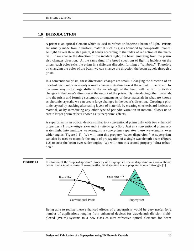
1.0 INTRODUCTION
A prism is an optical element which is used to refract or disperse a beam of light. Prismsare usually made from a uniform material such as glass bounded by non-parallel planes.As light travels through a prism, it bends according to the index of refraction of the mate-rial. If we change the direction of the incident light, the beam emerging from the prismalso changes direction. At the same time, if a broad spectrum of light is incident on theprism, each color exits the prism in a different direction forming a “rainbow.” Thereforeby changing the color of the beam we can change the direction the beam travels through aprism.
In a conventional prism, these directional changes are small. Changing the direction of anincident beam introduces only a small change in its direction at the output of the prism. Inthe same way, only large shifts in the wavelength of the beam will result in noticiblechanges in the beam’s direction at the output of the prism. By introducing other materialsinto the prism and forming systematic arrangements of these materials in what are knownas photonic crystals, we can create large changes in the beam’s direction. Creating a pho-tonic crystal by stacking alternating layers of material, by creating checkerboard lattices ofmaterial, or by introducing any other type of periodic variation in material allows us tocreate larger prism effects known as “superprism” effects.
A superprism is an optical device similar to a conventional prism only with two enhancedproperties: (1) super-dispersion and (2) ultra-refraction. Just as a conventional prism sep-arates light into multiple wavelengths, a superprism separates these wavelengths overwider angles (Figure 1.1). We will term this property "super-dispersion." A superprismcan also be used to magnify the angle of propagation of a single wavelength beam (Figure1.2) to steer the beam over wider angles. We will term this second property "ultra-refrac-tion."
FIGURE 1.1 Illustration of the "super-dispersion" property of a superprism versus dispersion in a conventionalprism. For a smaller range of wavelengths, the dispersion in a superprism is much stronger [1].
Being able to realize these enhanced effects of a superprism would be very useful for anumber of applications ranging from enhanced devices for wavelength division multi-plexed (WDM) systems to a new class of ultra-refractive optical elements for beam
Conventional Prism Superprism
Blue to Red Small range of λ

INTRODUCTION
14 Design and Fabrication of a Superprism using 2D Photonic Crystals
manipulation [2]. An additional advantage of the superprism is that it can reduce the sizeof many of these optical systems [3]. Large spectral separation and bending of incidentlight can be more compactly controlled using one small superprism rather than a largersystem composed of multiple prisms, lenses, and mirrors.
FIGURE 1.2 Illustration of ultra-refraction in a superprism. A small swing in the incident angle results in a largeswing in the output angle.
A number of groups have previously designed and fabricated photonic crystal devices forthe purpose of observing superprism effects. Kosaka, et al. used a three-dimensional pho-tonic crystal to demonstrate super-dispersion and ultra-refraction [1], [2]. The device wasfabricated as a 3D hexagonal lattice using self-assembling silicon and silicon oxide layers.For a wavelength difference of 0.01µm, they demonstrated a 50 degree difference in thebeam’s direction of propagation within the device. In a conventional silicon prism, thisshift would be less than one degree. They also demonstrated that changing the incidentangle from +/-7 degrees at the input results in a swing of +/- 70 degree within the crystal.Though these results seem promising as a demonstration of superprism phenomena inphotonic crystals, such a three dimensional structure is complicated to fabricate. In addi-tion, the Kosaka experiment does not report on the angular characteristics of the beamonce it exits the photonic crystal. This is probably due to the fact that once the beam exitsthe crystal, the superprism effect will reverse itself as the beam "refracts back" at the out-put of the device.
In order to circumvent the fabrication complexities associated with the 3D superprismwhile preserving the superprism effect at the output, Nelson, et al. demonstrated thatstrong wavelength dispersion effects can be achieved using a simpler one dimensionalphotonic crystal [3]. Nelson introduces a wavelength dependence into the angle of propa-gation by using the dispersion properties of a dielectric stack. As a beam propagateswithin the dielectric stack, the dispersion between wavelengths translates into a lateralshift in the position of the beam upon exiting the crystal. The dispersive effect is main-tained as the beam exits the device. While the fabrication of this 1D structure is indeedsimpler, this device shifts the location of the output beam rather than affecting its angle ofpropagation. In addition, the multiple reflections within the dielectric stack introduceheavy losses into the system.
Incident Beam Output Beam
Large AnglesSmall Angles
Superprism

INTRODUCTION
Design and Fabrication of a Superprism using 2D Photonic Crystals 15
We believe that the superprism effects of super-dispersion and angular magnification canbe achieved using 2D photonic crystals. By using a 2D structure, we can keep the fabrica-tion complexity relatively simple, while creating effects that are angular in nature. Inaddition, our device design proposes a way in which these superprism effects can beobserved not only within the crystal, but at the output as well.

DESIGN THEORY & SIMULATION
16 Design and Fabrication of a Superprism using 2D Photonic Crystals
2.0 DESIGN THEORY & SIMULATION
2.1 How can we make a prism “super”?
The prism effect in a conventional prism is due to different frequencies refracting at differ-ent angles within a material according to Snell's Law. We can illustrate this fundamentaleffect using dispersion surfaces as shown in Figure 2.3.
FIGURE 2.3 (a) The dispersion surface of an arbitrary isotropic medium showing the direction of the k-vectorand the direction of power propagation [4]. (b.) The dispersion surfaces for multiple frequencies inan isotropic medium. Each frequency has a dispersion surface of a different radius.
A dispersion surface maps out the angular dependence of the wave vector k for the propa-gation of light within a particular medium. For instance, in a medium of uniform refrac-tive index (an isotropic medium) the dispersion surface is a circle. That is, for a givenfrequency, the magnitude of the wave vector remains constant for every direction of prop-agation in the material. The dispersion relation determines the length of the wave vectoraccording to:
(EQ 2.1)
Therefore for each frequency, the radius of the dispersion surface will be different due tothe change in ω and ε. The wave vector will propagate in the direction normal to the dis-persion surface according to the group velocity:
(EQ 2.2)
In an anisotropic medium, as shown in Figure 2.4, the dielectric constant is no longer uni-form in all directions implying that the dispersion surface is no longer a circle. In a uniax-ial medium, for example, the dielectric constant along one principal axis, the optic axis, isdifferent from the dielectric constant along the other two axes. For this type of medium,the component of the wave polarized along the optic axis (extraordinary wave), has an
(b)(a)
k ω µε=
vg ∇kω=
DESIGN THEORY & SIMULATION
Design and Fabrication of a Superprism using 2D Photonic Crystals 17
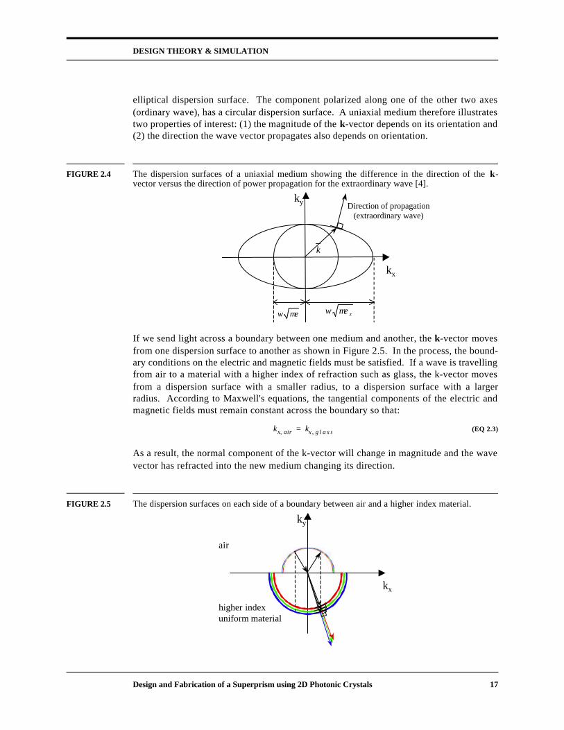
elliptical dispersion surface. The component polarized along one of the other two axes(ordinary wave), has a circular dispersion surface. A uniaxial medium therefore illustratestwo properties of interest: (1) the magnitude of the k-vector depends on its orientation and(2) the direction the wave vector propagates also depends on orientation.
FIGURE 2.4 The dispersion surfaces of a uniaxial medium showing the difference in the direction of the k-vector versus the direction of power propagation for the extraordinary wave [4].
If we send light across a boundary between one medium and another, the k-vector movesfrom one dispersion surface to another as shown in Figure 2.5. In the process, the bound-ary conditions on the electric and magnetic fields must be satisfied. If a wave is travellingfrom air to a material with a higher index of refraction such as glass, the k-vector movesfrom a dispersion surface with a smaller radius, to a dispersion surface with a largerradius. According to Maxwell's equations, the tangential components of the electric andmagnetic fields must remain constant across the boundary so that:
(EQ 2.3)
As a result, the normal component of the k-vector will change in magnitude and the wavevector has refracted into the new medium changing its direction.
FIGURE 2.5 The dispersion surfaces on each side of a boundary between air and a higher index material.
kx
ky Direction of propagation(extraordinary wave)
zµεω
k
µεω
kx air, kx g l a s s,=
kx
ky
air
higher indexuniform material

DESIGN THEORY & SIMULATION
18 Design and Fabrication of a Superprism using 2D Photonic Crystals
We can now use this model of dispersion surfaces to identify the effects we are looking forin a superprism: large angular magnification, and the super-dispersion of frequencies. Inorder to observe large angular magnification and super-dispersion, we need to find a mate-rial in which the properties of the k-vector are highly sensitive to changes in direction; i.e.a material that is highly anisotropic.
Consider, for example, a material with a dispersion surface such as the one shown inFigure 2.6.
FIGURE 2.6 Superprism effects using large changes in the group velocity. (a) Illustration of angularmagnification at a constant frequency in a superprism. (b) Illustration of super-dispersion in thesuperprism.
The sharp bends in the dispersion surface allow us to create highly dispersive effects usingvariations in the group velocity. The group velocity depends on the slope of the dispersionsurface. For orientations of the k-vector in the direction of the sharp bend, the groupvelocity is highly sensitive to changes in direction. As shown in Figure 2.6(a), at smallangles, a small change in the incident angle (shown with the black and gray arrows) willresult in a large change in the group velocity--the direction of propagation of the k-vector.The phase matching condition on the tangential k-vector is met as the wave crosses theboundary.
Figure 2.6(b) illustrates super-dispersion using a material with the same dispersion sur-face as in Figure 2.6(a). As stated previously, the radius of the dispersion surface changeswith frequency. Thus the super-dispersion of different frequencies is due to the fact thatfor a given k-vector, the difference in the group velocity for each frequency is very large,i.e. the slope of the dispersion surface changes very rapidly with frequency. Note that thedispersion surfaces corresponding to different frequencies in the uniform material aremuch closer together than the dispersion surfaces in the superprism. This result enhancesthe super-dispersion effect.
kx
ky
kx
ky
uniform material
superprism
(a) (b)
DESIGN THEORY & SIMULATION
Design and Fabrication of a Superprism using 2D Photonic Crystals 19
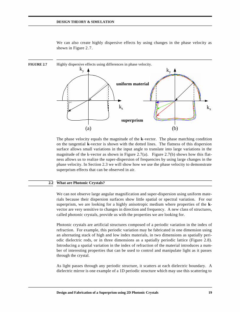
We can also create highly dispersive effects by using changes in the phase velocity asshown in Figure 2.7.
FIGURE 2.7 Highly dispersive effects using differences in phase velocity.
The phase velocity equals the magnitude of the k-vector. The phase matching conditionon the tangential k-vector is shown with the dotted lines. The flatness of this dispersionsurface allows small variations in the input angle to translate into large variations in themagnitude of the k-vector as shown in Figure 2.7(a). Figure 2.7(b) shows how this flat-ness allows us to realize the super-dispersion of frequencies by using large changes in thephase velocity. In Section 2.3 we will show how we use the phase velocity to demonstratesuperprism effects that can be observed in air.
2.2 What are Photonic Crystals?
We can not observe large angular magnification and super-dispersion using uniform mate-rials because their dispersion surfaces show little spatial or spectral variation. For oursuperprism, we are looking for a highly anisotropic medium where properties of the k-vector are very sensitive to changes in direction and frequency. A new class of structures,called photonic crystals, provide us with the properties we are looking for.
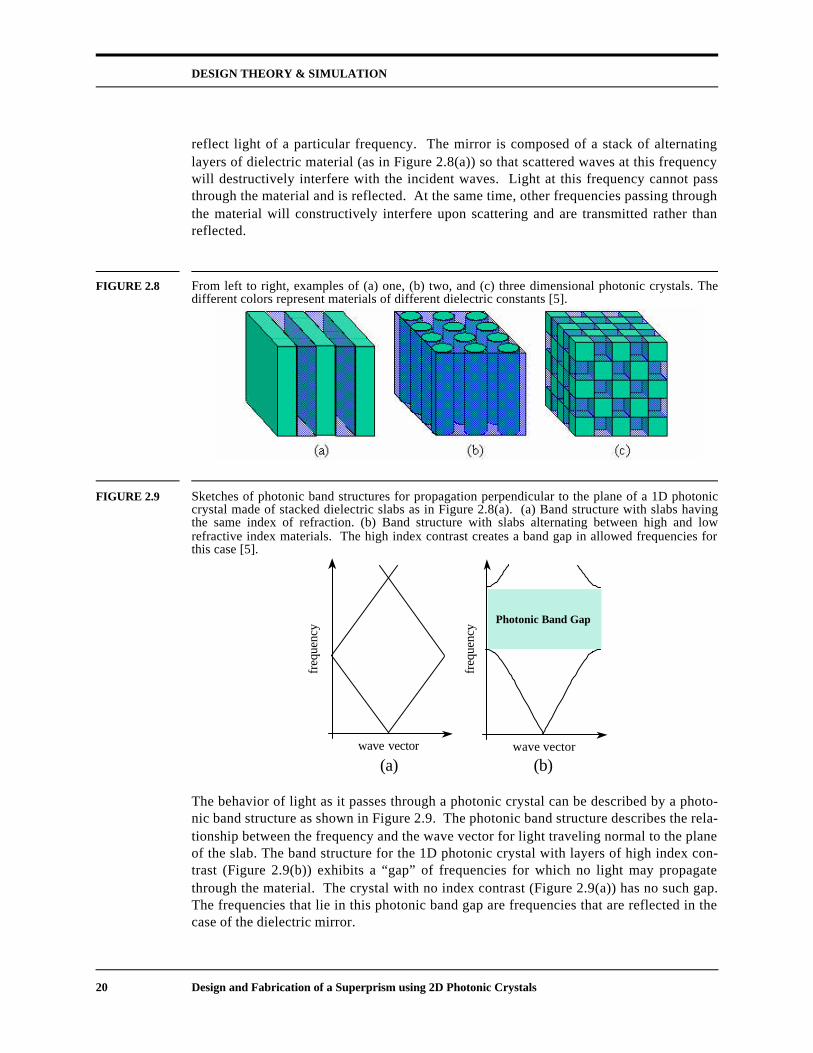
Photonic crystals are artificial structures composed of a periodic variation in the index ofrefraction. For example, this periodic variation may be fabricated in one dimension usingan alternating stack of high and low index materials, in two dimensions as spatially peri-odic dielectric rods, or in three dimensions as a spatially periodic lattice (Figure 2.8).Introducing a spatial variation in the index of refraction of the material introduces a num-ber of interesting properties that can be used to control and manipulate light as it passesthrough the crystal.
As light passes through any periodic structure, it scatters at each dielectric boundary. Adielectric mirror is one example of a 1D periodic structure which may use this scattering to
kx
ky
kx
ky
uniform material
superprism
(a) (b)
DESIGN THEORY & SIMULATION
20 Design and Fabrication of a Superprism using 2D Photonic Crystals
reflect light of a particular frequency. The mirror is composed of a stack of alternatinglayers of dielectric material (as in Figure 2.8(a)) so that scattered waves at this frequencywill destructively interfere with the incident waves. Light at this frequency cannot passthrough the material and is reflected. At the same time, other frequencies passing throughthe material will constructively interfere upon scattering and are transmitted rather thanreflected.
FIGURE 2.8 From left to right, examples of (a) one, (b) two, and (c) three dimensional photonic crystals. Thedifferent colors represent materials of different dielectric constants [5].
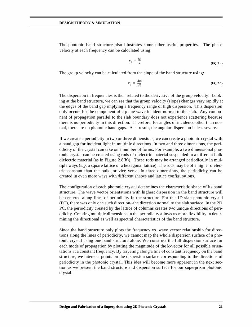
FIGURE 2.9 Sketches of photonic band structures for propagation perpendicular to the plane of a 1D photoniccrystal made of stacked dielectric slabs as in Figure 2.8(a). (a) Band structure with slabs havingthe same index of refraction. (b) Band structure with slabs alternating between high and lowrefractive index materials. The high index contrast creates a band gap in allowed frequencies forthis case [5].
The behavior of light as it passes through a photonic crystal can be described by a photo-nic band structure as shown in Figure 2.9. The photonic band structure describes the rela-tionship between the frequency and the wave vector for light traveling normal to the planeof the slab. The band structure for the 1D photonic crystal with layers of high index con-trast (Figure 2.9(b)) exhibits a “gap” of frequencies for which no light may propagatethrough the material. The crystal with no index contrast (Figure 2.9(a)) has no such gap.The frequencies that lie in this photonic band gap are frequencies that are reflected in thecase of the dielectric mirror.
Photonic Band Gap
freq
uenc
y
freq
uenc
y
wave vector wave vector
(a) (b)
DESIGN THEORY & SIMULATION
Design and Fabrication of a Superprism using 2D Photonic Crystals 21
The photonic band structure also illustrates some other useful properties. The phasevelocity at each frequency can be calculated using:
(EQ 2.4)
The group velocity can be calculated from the slope of the band structure using:
(EQ 2.5)
The dispersion in frequencies is then related to the derivative of the group velocity. Look-ing at the band structure, we can see that the group velocity (slope) changes very rapidly atthe edges of the band gap implying a frequency range of high dispersion. This dispersiononly occurs for the component of a plane wave incident normal to the slab. Any compo-nent of propagation parallel to the slab boundary does not experience scattering becausethere is no periodicity in this direction. Therefore, for angles of incidence other than nor-mal, there are no photonic band gaps. As a result, the angular dispersion is less severe.
If we create a periodicity in two or three dimensions, we can create a photonic crystal witha band gap for incident light in multiple directions. In two and three dimensions, the peri-odicity of the crystal can take on a number of forms. For example, a two dimensional pho-tonic crystal can be created using rods of dielectric material suspended in a different bulkdielectric material (as in Figure 2.8(b)). These rods may be arranged periodically in mul-tiple ways (e.g. a square lattice or a hexagonal lattice). The rods may be of a higher dielec-tric constant than the bulk, or vice versa. In three dimensions, the periodicity can becreated in even more ways with different shapes and lattice configurations.
The configuration of each photonic crystal determines the characteristic shape of its bandstructure. The wave vector orientations with highest dispersion in the band structure willbe centered along lines of periodicity in the structure. For the 1D slab photonic crystal(PC), there was only one such direction--the direction normal to the slab surface. In the 2DPC, the periodicity created by the lattice of columns creates two unique directions of peri-odicity. Creating multiple dimensions in the periodicity allows us more flexibility in deter-mining the directional as well as spectral characteristics of the band structure.
Since the band structure only plots the frequency vs. wave vector relationship for direc-tions along the lines of periodicity, we cannot map the whole dispersion surface of a pho-tonic crystal using one band structure alone. We construct the full dispersion surface foreach mode of propagation by plotting the magnitude of the k-vector for all possible orien-tations at a constant frequency. By traveling along a line of constant frequency on the bandstructure, we intersect points on the dispersion surface corresponding to the directions ofperiodicity in the photonic crystal. This idea will become more apparent in the next sec-tion as we present the band structure and dispersion surface for our superprism photoniccrystal.
vpωk----=
vgdωdk-------=
DESIGN THEORY & SIMULATION
22 Design and Fabrication of a Superprism using 2D Photonic Crystals
2.3 Superprism Design and Simulation
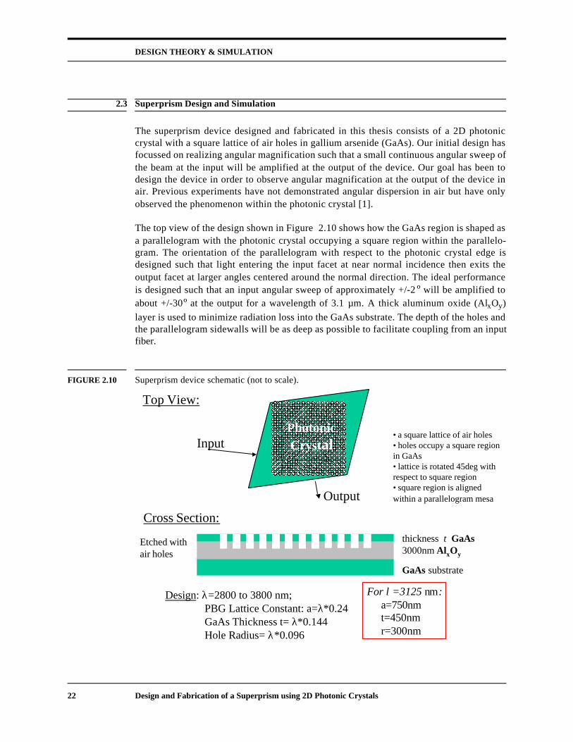
The superprism device designed and fabricated in this thesis consists of a 2D photoniccrystal with a square lattice of air holes in gallium arsenide (GaAs). Our initial design hasfocussed on realizing angular magnification such that a small continuous angular sweep ofthe beam at the input will be amplified at the output of the device. Our goal has been todesign the device in order to observe angular magnification at the output of the device inair. Previous experiments have not demonstrated angular dispersion in air but have onlyobserved the phenomenon within the photonic crystal [1].
The top view of the design shown in Figure 2.10 shows how the GaAs region is shaped asa parallelogram with the photonic crystal occupying a square region within the parallelo-gram. The orientation of the parallelogram with respect to the photonic crystal edge isdesigned such that light entering the input facet at near normal incidence then exits theoutput facet at larger angles centered around the normal direction. The ideal performanceis designed such that an input angular sweep of approximately +/-2 º will be amplified toabout +/-30º at the output for a wavelength of 3.1 µm. A thick aluminum oxide (AlxOy)layer is used to minimize radiation loss into the GaAs substrate. The depth of the holes andthe parallelogram sidewalls will be as deep as possible to facilitate coupling from an inputfiber.
FIGURE 2.10 Superprism device schematic (not to scale).
Cross Section:thickness t GaAs3000nm AlxOy
GaAs substrate
Etched withair holes
Output
InputPhotonicCrystal
Top View:
Design: λ=2800 to 3800 nm; PBG Lattice Constant: a=λ*0.24 GaAs Thickness t= λ*0.144Hole Radius= λ*0.096
• a square lattice of air holes• holes occupy a square regionin GaAs• lattice is rotated 45deg withrespect to square region• square region is alignedwithin a parallelogram mesa
For λ=3125 nm: a=750nm t=450nm r=300nm
DESIGN THEORY & SIMULATION
Design and Fabrication of a Superprism using 2D Photonic Crystals 23
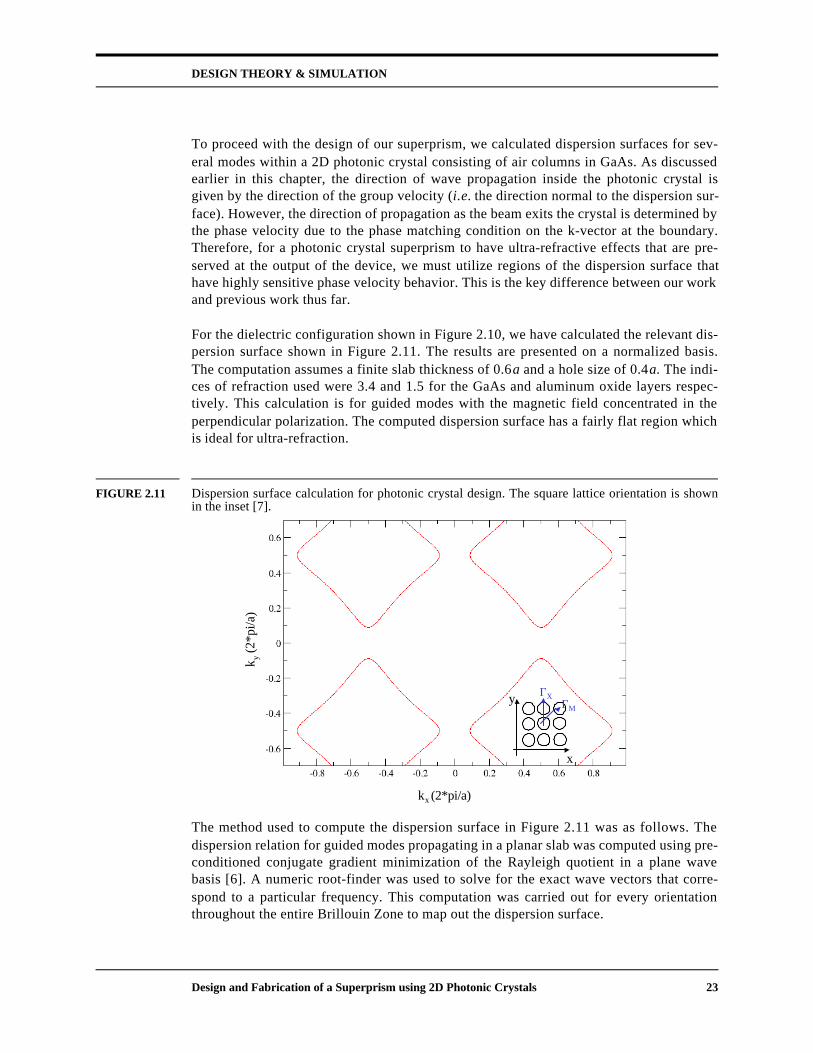
To proceed with the design of our superprism, we calculated dispersion surfaces for sev-eral modes within a 2D photonic crystal consisting of air columns in GaAs. As discussedearlier in this chapter, the direction of wave propagation inside the photonic crystal isgiven by the direction of the group velocity (i.e. the direction normal to the dispersion sur-face). However, the direction of propagation as the beam exits the crystal is determined bythe phase velocity due to the phase matching condition on the k-vector at the boundary.Therefore, for a photonic crystal superprism to have ultra-refractive effects that are pre-served at the output of the device, we must utilize regions of the dispersion surface thathave highly sensitive phase velocity behavior. This is the key difference between our workand previous work thus far.
For the dielectric configuration shown in Figure 2.10, we have calculated the relevant dis-persion surface shown in Figure 2.11. The results are presented on a normalized basis.The computation assumes a finite slab thickness of 0.6a and a hole size of 0.4a. The indi-ces of refraction used were 3.4 and 1.5 for the GaAs and aluminum oxide layers respec-tively. This calculation is for guided modes with the magnetic field concentrated in theperpendicular polarization. The computed dispersion surface has a fairly flat region whichis ideal for ultra-refraction.
FIGURE 2.11 Dispersion surface calculation for photonic crystal design. The square lattice orientation is shownin the inset [7].
The method used to compute the dispersion surface in Figure 2.11 was as follows. Thedispersion relation for guided modes propagating in a planar slab was computed using pre-conditioned conjugate gradient minimization of the Rayleigh quotient in a plane wavebasis [6]. A numeric root-finder was used to solve for the exact wave vectors that corre-spond to a particular frequency. This computation was carried out for every orientationthroughout the entire Brillouin Zone to map out the dispersion surface.
kx (2*pi/a)
k y (2*
pi/a
)
y
x
ΓXΓM
DESIGN THEORY & SIMULATION
24 Design and Fabrication of a Superprism using 2D Photonic Crystals
FIGURE 2.12 The band structure for the superprism photonic crystal [7].
FIGURE 2.13 Explanation of Superprism ultra-refraction using the dispersion surfaces in the photonic crystal andGaAs [7].
Group velocity direction
Input Facet Output Facet
GaAsDispersion Surface
Photonic CrystalDispersion Surface
Photonic CrystalDispersion Surface GaAs
Dispersion Surface
kiki
kf
kf
ki : Incident wavevector kf : Final wavevector
Phase velocity direction
kx
ky ΓM
ΓX
DESIGN THEORY & SIMULATION
Design and Fabrication of a Superprism using 2D Photonic Crystals 25
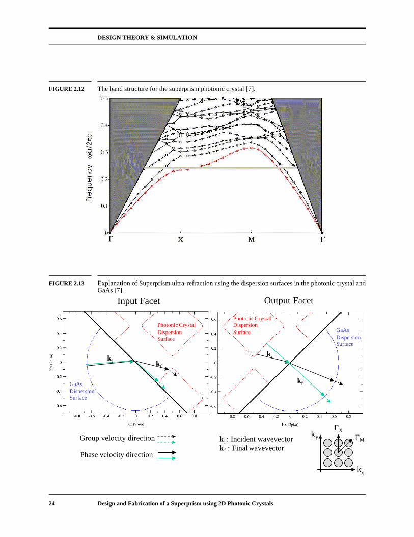
Figure 2.12 is the band structure for the superprism’s photonic crystal. The computationuses the same assumptions as the dispersion surface calculation in Figure 2.11. The hori-zontal line represents an equi-frequency line at the normalized design frequency of 0.24.
Our device operates by coupling to the lowest mode shown in this band structure. Asstated earlier, we have assumed an input beam polarized such that the magnetic field isconcentrated in the z direction. The lowest order mode corresponds to this polarization andis therefore the only mode that the input beam will couple to. Though the equi-frequencyline intersects other higher modes, these modes correspond to other polarizations with theelectric field concentrated in the z direction. In addition, the orientation of our photoniccrystal is such that the beam is incident upon the GaAs/photonic crystal boundary at anangle and will only couple to the lowest order mode independent of polarization. Thisresult is more clearly illustrated in Figure 2.13.
The ultra-refraction property of our superprism is illustrated in Figure 2.13. The boundarybetween the gallium arsenide and the photonic crystal lies along the Γ-M symmetry line ofthe square lattice. The two different arrows in Figure 2.13 represent k-vectors for two dif-ferent input beams which differ by only a small angle. As the beam propagates from GaAsinto the photonic crystal, the phase matching condition on the tangential component of thek-vector must be met. The beam refracts into the photonic crystal as the k-vector movesfrom the GaAs dispersion surface to the photonic crystal dispersion surface.
The small difference between the two input wave vectors translates into a large change inthe phase velocity inside the photonic crystal due to the flatness of the dispersion surface.As the two beams exit the photonic crystal at the output facet, the phase matching condi-tion is met again and the angle between the wave vectors is greatly magnified.
Figure 2.13 does not show the beams as they propagate from air to GaAs at the input andfrom GaAs to air at the output. However, the angular difference between the two beamswill only be enhanced as the beams propagate into air. The result is a large angular sweepat the output for a very small angular sweep at the input. Similar considerations can alsobe used to realize frequency super-dispersion using a broadband source at a fixed angle ofincidence.
The photonic crystal dispersion surfaces shown in Figure 2.11 and Figure 2.13 corre-spond to the lowest order mode shown in the band structure in Figure 2.12. By travelingalong a line of constant frequency on the band structure, we intersect points on the disper-sion surface corresponding to k-vectors in the directions of periodicity in the photoniccrystal, which are the Γ-M and Γ-X directions for a square lattice. If there are multiplemodes at a particular frequency, there are multiple dispersion surfaces.
Traveling along the equi-frequency line in Figure 2.12, we intersect both the lowest ordermode, and two higher order modes. These two higher order modes have dispersion sur-faces shaped like circles with smaller radii. For near normal incidence, an input beam maybe able to couple to these modes-though the coupling may be weak due to differences inpolarization. However, we have designed the input facets such that the beam is incident
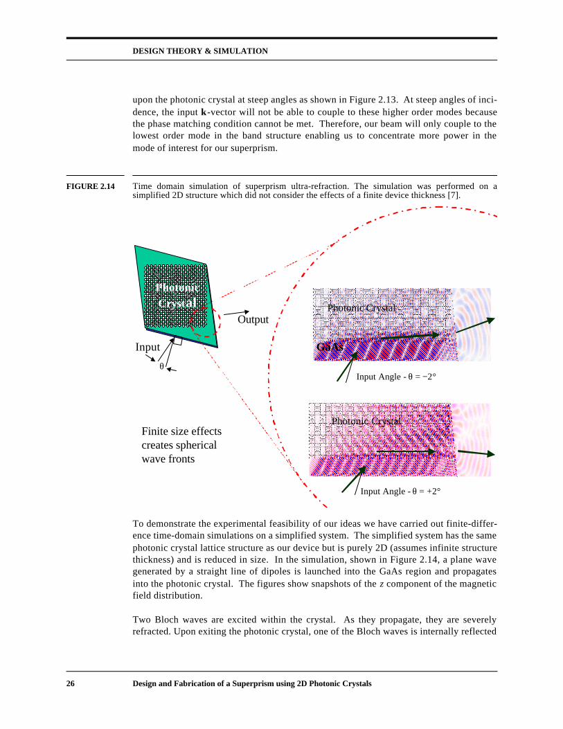
DESIGN THEORY & SIMULATION
26 Design and Fabrication of a Superprism using 2D Photonic Crystals
upon the photonic crystal at steep angles as shown in Figure 2.13. At steep angles of inci-dence, the input k-vector will not be able to couple to these higher order modes becausethe phase matching condition cannot be met. Therefore, our beam will only couple to thelowest order mode in the band structure enabling us to concentrate more power in themode of interest for our superprism.
FIGURE 2.14 Time domain simulation of superprism ultra-refraction. The simulation was performed on asimplified 2D structure which did not consider the effects of a finite device thickness [7].
To demonstrate the experimental feasibility of our ideas we have carried out finite-differ-ence time-domain simulations on a simplified system. The simplified system has the samephotonic crystal lattice structure as our device but is purely 2D (assumes infinite structurethickness) and is reduced in size. In the simulation, shown in Figure 2.14, a plane wavegenerated by a straight line of dipoles is launched into the GaAs region and propagatesinto the photonic crystal. The figures show snapshots of the z component of the magneticfield distribution.
Two Bloch waves are excited within the crystal. As they propagate, they are severelyrefracted. Upon exiting the photonic crystal, one of the Bloch waves is internally reflected
Output
Input
PhotonicCrystal Photonic Crystal
GaAs
Input Angle - θ = −2°
Input Angle - θ = +2°
Photonic CrystalFinite size effectscreates sphericalwave fronts
θ

DESIGN THEORY & SIMULATION
Design and Fabrication of a Superprism using 2D Photonic Crystals 27
at the GaAs/Air interface allowing a single Bloch wave to couple out into air. As theincoming beam is changed by +/-2º, the output beam sweeps through a large angular rangeof +/-30º. In the high dielectric GaAs region, a fringe pattern can be observed due to inter-ference between the incident and reflected beams. The finite size of the simulation alsocauses the output beam to appear spherical. The arrows within the figures are just to guidethe eye but demonstrate how the direction of the beam shifts with the slight change in theinput angle.
RESEARCH APPROACH
28 Design and Fabrication of a Superprism using 2D Photonic Crystals
3.0 RESEARCH APPROACH
3.1 Research Objective
Our goal is to design and fabricate a superprism device using a two dimensional photoniccrystal in a gallium arsenide material system. The device will allow a small angular sweepat the input to translate into a large angular sweep at the output (i.e. ultra-refraction). Inaddition, an input beam with a small spread in frequencies will result in a large angularseparation of these frequencies at the output (super-dispersion).
The superprism is composed of a two dimensional photonic crystal with a square lattice ofair holes in gallium arsenide (see Figure 2.10). The photonic crystal rests on a thick layerof aluminum oxide on a gallium arsenide substrate. The depth of the air holes is as deep aspossible. The feature sizes of the photonic crystal are scalable depending on the wave-length of operation. Our desired wavelength range of 2.8 to 3.8 µm implies a lattice con-stant of 672 to 912 nm, and a hole radius varying between 269 and 365 nm. The input andoutput facets are air-GaAs boundaries positioned at specific design angles with respect tothe photonic crystal. The total thickness of the device (excluding substrate) is about 3.5µm while the top surface will have an area of about 2 cm x 2 cm.
The orientation of the parallelogram with respect to the photonic crystal edge is designedsuch that light entering the input facet at near normal incidence, then exits the output facetat magnified angles centered around the normal direction. The ideal performance isdesigned such that an input angular sweep of approximately +/- 2º will be amplified toabout +/- 30º at the output for a wavelength of 3.1 µm.
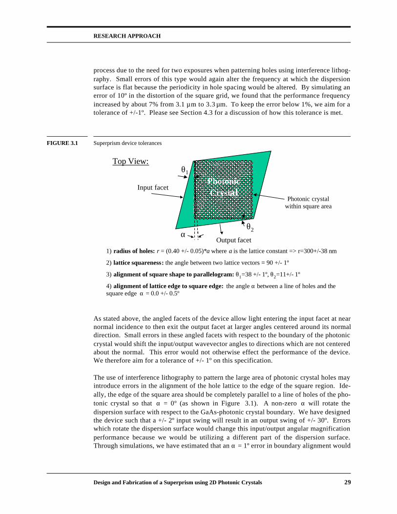
3.2 Design Tolerances
In order to identify the steps necessary to fabricate the superprism, we needed to deter-mine a number of tolerances on the device design. The results are presented in Figure 3.1.
Changing the ratio of hole size to lattice constant (r/a) changes the frequency at which thedispersion surface is flat thereby shifting the frequency at which we will observe our per-formance specifications. By simulating a change in r/a from 0.40 to 0.35 and recalculat-ing the dispersion surface, we found that the frequency at which the dispersion surfacewas now flat (the performance frequency) decreased by about 7%. An error in r/a by -0.05 would shift our performance frequency from 3.1 µm to 2.9 µm which is acceptablefrom a testing perspective. We therefore aim to stay within this error of 7% or r = 300 nm+/- 38 nm. However, since the hole size is susceptible to a number of sources of variationfrom the lithography as well as etching steps, this parameter is anticipated to be the mostdifficult parameter to meet.
Lattice squareness refers to the degree to which the grid of holes in the photonic crystal isactually square. Errors in the squareness of the grid may be introduced in the fabrication
RESEARCH APPROACH
Design and Fabrication of a Superprism using 2D Photonic Crystals 29
process due to the need for two exposures when patterning holes using interference lithog-raphy. Small errors of this type would again alter the frequency at which the dispersionsurface is flat because the periodicity in hole spacing would be altered. By simulating anerror of 10º in the distortion of the square grid, we found that the performance frequencyincreased by about 7% from 3.1 µm to 3.3 µm. To keep the error below 1%, we aim for atolerance of +/-1º. Please see Section 4.3 for a discussion of how this tolerance is met.
FIGURE 3.1 Superprism device tolerances
As stated above, the angled facets of the device allow light entering the input facet at nearnormal incidence to then exit the output facet at larger angles centered around its normaldirection. Small errors in these angled facets with respect to the boundary of the photoniccrystal would shift the input/output wavevector angles to directions which are not centeredabout the normal. This error would not otherwise effect the performance of the device.We therefore aim for a tolerance of +/- 1º on this specification.
The use of interference lithography to pattern the large area of photonic crystal holes mayintroduce errors in the alignment of the hole lattice to the edge of the square region. Ide-ally, the edge of the square area should be completely parallel to a line of holes of the pho-tonic crystal so that α = 0º (as shown in Figure 3.1). A non-zero α will rotate thedispersion surface with respect to the GaAs-photonic crystal boundary. We have designedthe device such that a +/- 2º input swing will result in an output swing of +/- 30º. Errorswhich rotate the dispersion surface would change this input/output angular magnificationperformance because we would be utilizing a different part of the dispersion surface.Through simulations, we have estimated that an α = 1º error in boundary alignment would
1) radius of holes: r = (0.40 +/- 0.05)*a where a is the lattice constant => r=300+/-38 nm
2) lattice squareness: the angle between two lattice vectors = 90 +/- 1º
3) alignment of square shape to parallelogram: θ1=38 +/- 1º, θ2=11+/- 1º
4) alignment of lattice edge to square edge: the angle α between a line of holes and thesquare edge α = 0.0 +/- 0.5º
Output facet
Input facet
Top View:θ1
θ2α
Photonic crystalwithin square area
PhotonicCrystal
RESEARCH APPROACH
30 Design and Fabrication of a Superprism using 2D Photonic Crystals
change our design performance in two ways depending on whether α is positive or nega-tive: a +/- 1.5º input translating to +/- 30º output, or +/- 2.5º input translating to +/- 30ºoutput. We therefore set our tolerance on this alignment specification to α = 0 +/- 0.5º.
3.3 Fabrication Sequence
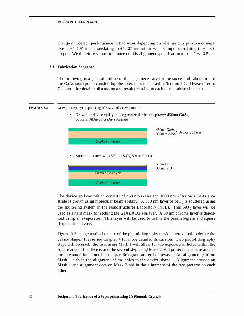
The following is a general outline of the steps necessary for the successful fabrication ofthe GaAs superprism considering the tolerances discussed in Section 3.2. Please refer toChapter 4 for detailed discussion and results relating to each of the fabrication steps.
FIGURE 3.2 Growth of epilayer, sputtering of SiO2 and Cr evaporation
The device epilayer which consists of 450 nm GaAs and 3000 nm AlAs on a GaAs sub-strate is grown using molecular beam epitaxy. A 300 nm layer of SiO2 is sputtered usingthe sputtering system in the Nanostructures Laboratory (NSL). This SiO2 layer will beused as a hard mask for etching the GaAs/AlAs epilayer. A 50 nm chrome layer is depos-ited using an evaporator. This layer will be used to define the parallelogram and squareshape of the device.
Figure 3.3 is a general schematic of the photolithography mask patterns used to define thedevice shape. Please see Chapter 4 for more detailed discussion. Two photolithographysteps will be used: the first using Mask 1 will allow for the exposure of holes within thesquare area of the device, and the second step using Mask 2 will protect the square area asthe unwanted holes outside the parallelogram are etched away. An alignment grid onMask 1 aids in the alignment of the holes to the device shape. Alignment crosses onMask 1 and alignment dots on Mask 2 aid in the alignment of the two patterns to eachother.
GaAs substrate
450nm GaAs3000nm AlAs
• Growth of device epilayer using molecular beam epitaxy: 450nm GaAs,3000nm AlAs on GaAs substrate
GaAs substrate
50nm Cr300nm SiO2
• Substrate coated with 300nm SiO2, 50nm chrome
Device Epilayer
Device Epilayer
RESEARCH APPROACH
Design and Fabrication of a Superprism using 2D Photonic Crystals 31
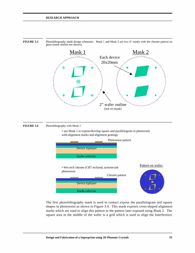
FIGURE 3.3 Photolithography mask design schematic. Mask 1 and Mask 2 are two 4” masks with the chrome pattern onglass (mask outline not shown).
FIGURE 3.4 Photolithography with Mask 1
The first photolithography mask is used to contact expose the parallelogram and squareshapes in photoresist as shown in Figure 3.4. This mask exposes cross-shaped alignmentmarks which are used to align this pattern to the pattern later exposed using Mask 2. Thesquare area in the middle of the wafer is a grid which is used to align the Interference
Mask 1 Mask 2 Each device
20x20mm
2” wafer outline(not on mask)
• use Mask 1 to expose/develop square and parallelogram in photoresistwith alignment marks and alignment gratings
GaAs substrate
Photoresist pattern
Device Epilayer
GaAs substrate
Device Epilayer
Chrome pattern
• Wet etch chrome (CR7 etchant); acetone/ashphotoresist
Pattern on wafer:

RESEARCH APPROACH
32 Design and Fabrication of a Superprism using 2D Photonic Crystals
Lithography exposure to this Mask 1 pattern. A wet etch is used to transfer the resist pat-tern to the chrome layer.
FIGURE 3.5 Interference Lithography with use of trilayer resist stack. Please see Chapter 4 for a discussion of thicknesses.
Figure 3.5 shows the preparation of the substrate and the subsequent Interference Lithog-raphy exposure. Interference lithography is used to pattern the whole wafer with holes.The trilayer resist stack consisting of: photoresist, SiO2 interlayer, and anti-reflective coat-ing (ARC) is used to minimize reflections off the substrate during the exposure and facili-tate pattern transfer to the SiO2 hard mask layer. Please see Chapter 4 for a discussion ofthe relevant thicknesses. The alignment grid on the wafer is used to align the hole patternto the device shape in chrome.
Figure 3.6 shows the transfer of the hole pattern to the SiO2 hard mask layer using Reac-tive Ion Etching (RIE). The gases used to etch the SiO2 and ARC layers are CHF3, andHe/O2 respectively. A CHF3 RIE step is then used to transfer the pattern into the SiO2hard mask layer. The chrome layer will prevent the etching of holes outside the squarearea within the parallelogram shape as shown by the pattern on the wafer in Figure 3.6. AHe/O2 ash step is used to remove any remaining ARC.
• Spin trilayer: thick Anti-reflective coating (ARC), thick SiO2 interlayer, photoresist
GaAs substrate
Device Epilayer
photoresistSiO2
ARC over pattern in chromeSiO2 hard mask
GaAs substrate
Device Epilayer
Holes in photoresistSiO2 interlayerARC over pattern in chromeSiO2 hard mask
• Expose/develop holes in photoresist using interference lithography (IL)• use mask 1 grid to align hole pattern to device shape

RESEARCH APPROACH
Design and Fabrication of a Superprism using 2D Photonic Crystals 33
FIGURE 3.6 Reactive Ion Etching of trilayer resist stack and SiO2 hard mask. The deep holes shown are only to illustratepattern transfer through each layer. As the hole pattern is transferred through each layer, layer thicknessesdecrease due to sputtering and etching thus avoiding unnecessary high aspect ratio etching.
FIGURE 3.7 Photolithography using Mask 2
The second photolithography step shown in Figure 3.7 uses Mask 2 to expose the deviceparallelogram shape with a closed square area to protect the holes inside. Alignmentmarks are used to align Mask 2 to the pattern from Mask 1. An RIE step is then used toetch away the holes in the SiO2 hard mask outside of the parallelogram area.
• Reactive Ion Etch (RIE) trilayer to transfer hole pattern
GaAs substrate
Device Epilayer
GaAs substrate
Device Epilayer
Holes exposed in photoresistHoles etched into SiO2 interlayerHoles etched in ARC
Holes etched in SiO2
• RIE SiO2 hard mask layer; O2 ash to remove ARC layer Pattern on wafer:
• Spin photoresist; contact expose/develop using mask 2• pattern from mask 2 is used to protect the parallelogram in order to etch mesa in SiO2• alignment marks on mask 2 used to align to pattern from mask 1
GaAs substrate
Device Epilayer
GaAs substrate
Device Epilayer
• RIE external SiO2; ash photoresist
Pattern on wafer:
RESEARCH APPROACH
34 Design and Fabrication of a Superprism using 2D Photonic Crystals
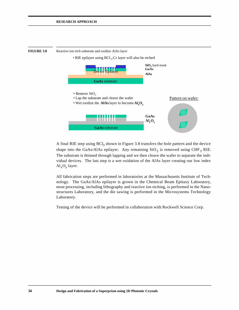
FIGURE 3.8 Reactive ion etch substrate and oxidize AlAs layer
A final RIE step using BCl3 shown in Figure 3.8 transfers the hole pattern and the deviceshape into the GaAs/AlAs epilayer. Any remaining SiO2 is removed using CHF3 RIE.The substrate is thinned through lapping and we then cleave the wafer to separate the indi-vidual devices. The last step is a wet oxidation of the AlAs layer creating our low indexAlxOy layer.
All fabrication steps are performed in laboratories at the Massachusetts Institute of Tech-nology. The GaAs/AlAs epilayer is grown in the Chemical Beam Epitaxy Laboratory,most processing, including lithography and reactive ion etching, is performed in the Nano-structures Laboratory, and the die sawing is performed in the Microsystems TechnologyLaboratory.
Testing of the device will be performed in collaboration with Rockwell Science Corp.
• RIE epilayer using BCl3; Cr layer will also be etched
GaAs substrate
• Remove SiO2
• Lap the substrate and cleave the wafer• Wet oxidize the AlAs layer to become AlxOy
GaAs substrate
GaAsAlxOy
Pattern on wafer:
SiO2 hard maskGaAsAlAs
Device Epilayer

DISCUSSION & RESULTS
Design and Fabrication of a Superprism using 2D Photonic Crystals 35
4.0 DISCUSSION & RESULTS
4.1 Molecular Beam Epitaxy Results
The GaAs heterostructure shown in Figure 4.1 was grown using the Riber Instruments gassource molecular beam epitaxy (GSMBE) system in the Chemical Beam Epitaxy group atMIT. The structure was grown successfully with the following layers:
• 400 nm GaAs
• 50 nm Al0.50Ga0.50As
• 3000 nm AlAs
• 50 nm Al0.50Ga0.50As
• GaAs substrate
The 50nm AlGaAs layers are intermediary layers which are helpful during the oxidationstep for stabilizing the GaAs interface. Please see Section 4.6 for discussion of theseresults. This intermediary layer will not oxidize and will therefore serve as a high indexlayer for guiding light. With this in mind, the top GaAs layer was grown to be 400 nm sothat the total high index layer thickness was 450 nm.
FIGURE 4.1 A scanning electron microscope (SEM) image of a randomly fractured edge of the GaAs heterostructureshowing the GaAs/AlGaAs/AlAs epilayer on the GaAs substrate. The 50nm AlGaAs layers are not clearlyvisible due to the non uniformity of the surface.
450nm GaAs/AlGaAs
3000nm AlAs
GaAs substrate
DISCUSSION & RESULTS
36 Design and Fabrication of a Superprism using 2D Photonic Crystals
4.2 Photolithography Results
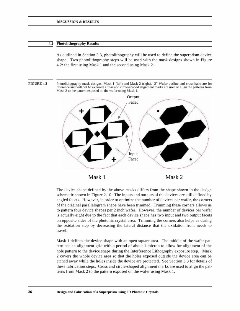
As outlined in Section 3.3, photolithography will be used to define the superprism deviceshape. Two photolithography steps will be used with the mask designs shown in Figure4.2: the first using Mask 1 and the second using Mask 2.
FIGURE 4.2 Photolithography mask designs: Mask 1 (left) and Mask 2 (right). 2” Wafer outline and cross-hairs are forreference and will not be exposed. Cross and circle-shaped alignment marks are used to align the patterns fromMask 2 to the pattern exposed on the wafer using Mask 1.
The device shape defined by the above masks differs from the shape shown in the designschematic shown in Figure 2.10. The inputs and outputs of the devices are still defined byangled facets. However, in order to optimize the number of devices per wafer, the cornersof the original parallelogram shape have been trimmed. Trimming these corners allows usto pattern four device shapes per 2 inch wafer. However, the number of devices per waferis actually eight due to the fact that each device shape has two input and two output facetson opposite sides of the photonic crystal area. Trimming the corners also helps us duringthe oxidation step by decreasing the lateral distance that the oxidation front needs totravel.
Mask 1 defines the device shape with an open square area. The middle of the wafer pat-tern has an alignment grid with a period of about 1 micron to allow for alignment of thehole pattern to the device shape during the Interference Lithography exposure step. Mask2 covers the whole device area so that the holes exposed outside the device area can beetched away while the holes inside the device are protected. See Section 3.3 for details ofthese fabrication steps. Cross and circle-shaped alignment marks are used to align the pat-terns from Mask 2 to the pattern exposed on the wafer using Mask 1.
InputFacet
OutputFacet
Mask 1 Mask 2

DISCUSSION & RESULTS
Design and Fabrication of a Superprism using 2D Photonic Crystals 37
4.3 Interference Lithography Results
Interference lithography is used to pattern the square lattice of holes for the 2D photonic crystal.Interference lithography is a more appropriate lithography technique for this superprism designthan photolithography or electron beam lithography because the hole pattern is periodic, covering alarge area, and with minimum feature sizes under 1µm.
4.3.1 Basic Overview of Interference Lithography
Interference lithography (IL) allows patterning of periodic structures over a large area.The periodic pattern is formed by the constructive and destructive interference of lightwaves which form a standing wave at the substrate surface. This standing wave exposes agrating pattern on the substrate as illustrated in Figure 4.3.
FIGURE 4.3 In interference lithography, the standing wave formed by the interference of two light beams exposes aperiodic grating on the substrate. In this schematic, the incoming waves are approximated as plane waveswhen in reality they are spherical.
The period of the grating (P) depends on the source wavelength (λ) and the half-anglebetween the two beams (θ) according to:
(EQ 4.6)
Two IL systems in the Nanostructures Laboratory (NSL) at MIT were investigated for pat-terning the photonic crystal used in this thesis: the Lloyd's mirror interferometer, and thetwo-beam interferometer.
θ
λ
Substrate
P
P λ2 θsin--------------=

DISCUSSION & RESULTS
38 Design and Fabrication of a Superprism using 2D Photonic Crystals
4.3.2 The Lloyd’s Mirror Interferometer
The Lloyd's mirror interferometer uses a broad beam of light and a mirror to create aninterference pattern on the substrate as shown in Figure 4.4. The mirror sits perpendicularto the substrate surface. The interference pattern is formed by the interference betweenlight directly incident on the substrate, and light reflected off the mirror which then hitsthe substrate. The period of the grating is given by Equation 4.6 with θ determined by theorientation of the mirror and substrate with respect to the incoming light.
FIGURE 4.4 Top view of the Lloyd's mirror interferometer system showing light incident upon the mirror and substratesimultaneously. The light reflected off the mirror interferes with the light directly incident upon the substrateto form a periodic pattern. The rotation stage sets the period by changing the orientation of the mirror andsubstrate.
The present Lloyd's mirror system as illustrated in Figure 4.4 uses a 325 nm HeCd laseras its source. The mirror which is perpendicular to the substrate is rigidly attached to thesubstrate chuck via vacuum suction. A rotation stage sets the period of the grating byrotating this mirror/substrate combination. The spatial filter removes high frequencynoise from the beam in order to create a clean Gaussian beam profile. A pinhole allowsthe beam diameter to expand so that it exposes a large area when it reaches the mirror/sub-strate.
FIGURE 4.5 A grating pattern in resist exposed using the Lloyd's mirror interferometer. The period is approximately 760nm.
1 µm
DISCUSSION & RESULTS
Design and Fabrication of a Superprism using 2D Photonic Crystals 39
Figure 4.5 shows a 760 nm period grating exposed in negative resist using the Lloyd’smirror interferometer. The resist pattern rests on an anti-reflective coating on a siliconsubstrate.
There are several advantages to the Lloyd's mirror system. Firstly, the Lloyd's mirror isfairly immune to external mechanical vibrations. Vibrations that affect the relative pathlength of the two interfering beams are the only vibrations that affect the pattern exposedon the substrate. Because the separation of the beam does not occur until reflection off themirror, and the mirror is rigidly connected to the substrate, such vibrations are minimal.The result is that the relative lengths of the two beams is very stable [8]. In the two-beamIL system, which is discussed next, the splitting of the beam requires a phase-locking sys-tem to stabilize the relative path length of the beams.
A second advantage of the Lloyd's mirror system is the ease with which the period of thegrating can be adjusted. Changing the period only requires changing the setting on themirror/substrate rotation stage. No additional alignment steps are necessary.
4.3.3 The Two Beam Interferometer
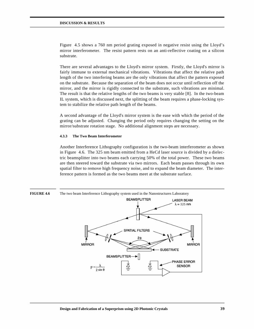
Another Interference Lithography configuration is the two-beam interferometer as shownin Figure 4.6. The 325 nm beam emitted from a HeCd laser source is divided by a dielec-tric beamsplitter into two beams each carrying 50% of the total power. These two beamsare then steered toward the substrate via two mirrors. Each beam passes through its ownspatial filter to remove high frequency noise, and to expand the beam diameter. The inter-ference pattern is formed as the two beams meet at the substrate surface.
FIGURE 4.6 The two beam Interference Lithography system used in the Nanostructures Laboratory
DISCUSSION & RESULTS
40 Design and Fabrication of a Superprism using 2D Photonic Crystals
A feedback system is used to correct for relative path length differences between the twobeams which may occur due to mechanical vibrations in the system. A beamsplitter abovethe substrate mount samples and recombines the two incoming beams as in a Mach-Zehnder interferometer. The two outputs of the beamsplitter are detected by two photo-diodes which are the inputs to a differential amplifier. The differential amplifier thendrives a piezomotor which adjusts the position of the first beamsplitter stage. Any changein the path length of either beam will cause the photodiode current to change. This changein current changes the position of the beamsplitter thus introducing a change in the relativepath length of the two beams. By keeping the photodiode current constant, the feedbacksystem can stabilize the phase difference between the two beams stabilizing the interfer-ence pattern at the substrate surface.
As explained earlier, the period of the grating is determined by the angle between the twointerfering beams. For the 750 nm period holes of our superprism, the half-angle betweenthe two beams must be 12.5 degrees. In order to adjust the period using the two-beaminterferometer, the spatial filters must be moved and the steering mirrors must be adjustedto the appropriate angle. This adjustment process requires a realignment of the beam paththrough all the optical elements which is not trivial and can take several hours.
From the perspective of stabilization and flexibility of the period, the Lloyd's mirror inter-ferometer is much easier to use. There is no need for additional feedback mechanisms tostabilize the fringe pattern nor is any adjustment process necessary to change the period.However, there are some distinct advantages that make the two-beam interferometer moreappropriate for patterning the 2D photonic crystal.
4.3.4 Fabricating Photonic Crystal Grids
So far we have only discussed patterning 1D gratings using interference lithography. Tofabricate 2D grids, two orthogonal grating exposures are necessary. This is accomplishedby placing the substrate on a rotation stage which is rotated by 90 degrees between expo-sures. As discussed in Section 3.2, the tolerance on the squareness of the grid is +/- 1degree. The resolution of the substrate rotation stage in the two beam IL system is lessthan one degree whereas on the Lloyd's mirror interferometer, no such stage exists andtherefore the substrate would have to be manually rotated.
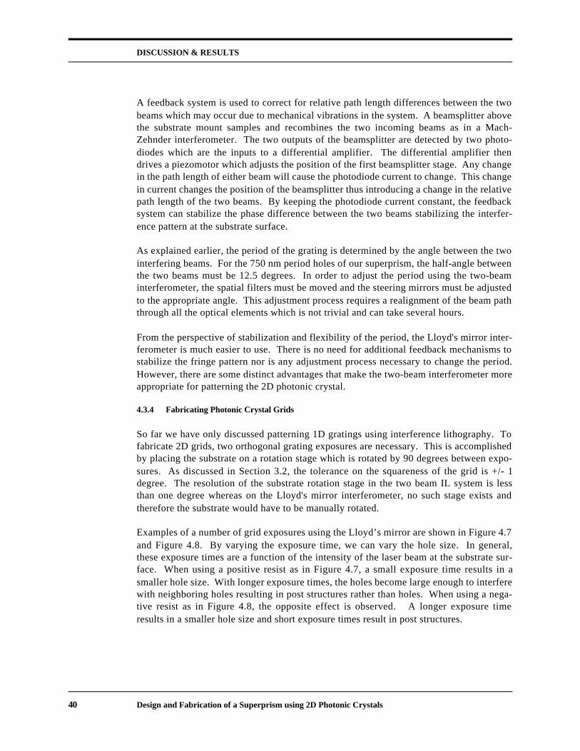
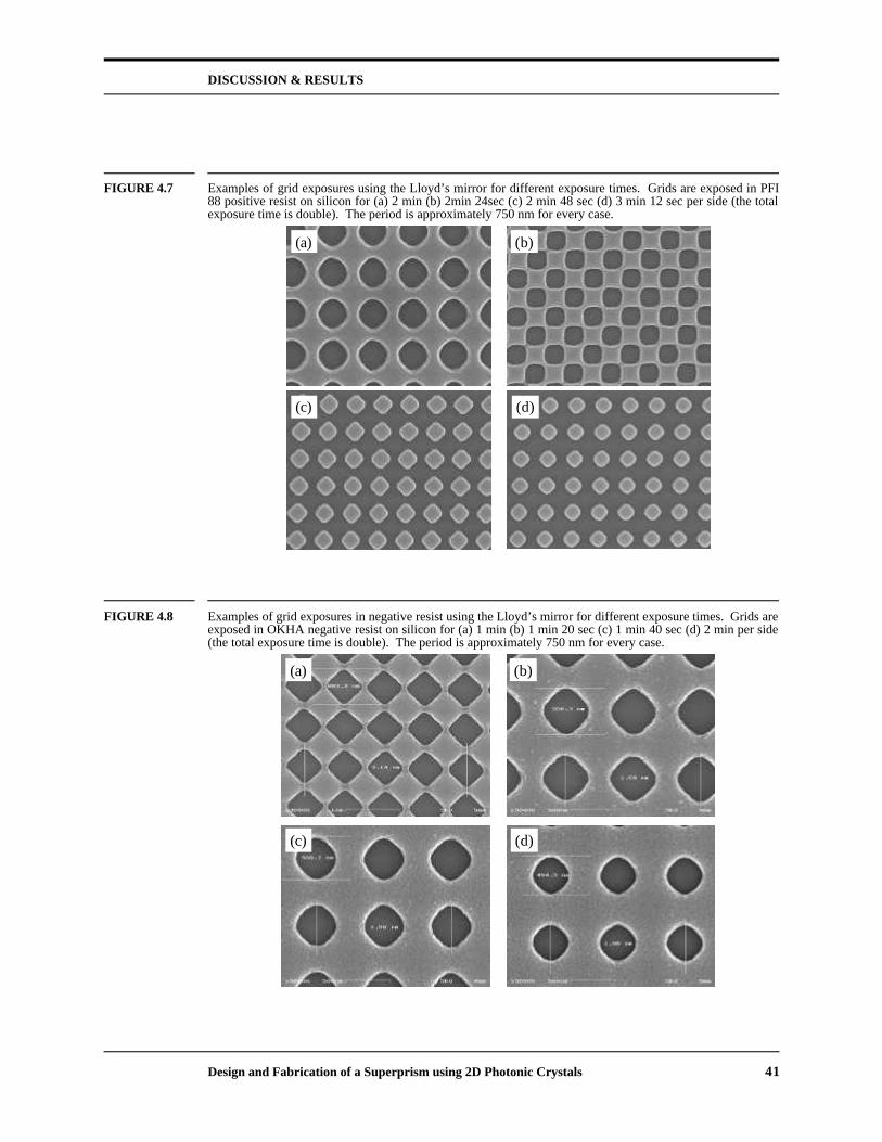
Examples of a number of grid exposures using the Lloyd’s mirror are shown in Figure 4.7and Figure 4.8. By varying the exposure time, we can vary the hole size. In general,these exposure times are a function of the intensity of the laser beam at the substrate sur-face. When using a positive resist as in Figure 4.7, a small exposure time results in asmaller hole size. With longer exposure times, the holes become large enough to interferewith neighboring holes resulting in post structures rather than holes. When using a nega-tive resist as in Figure 4.8, the opposite effect is observed. A longer exposure timeresults in a smaller hole size and short exposure times result in post structures.
DISCUSSION & RESULTS
Design and Fabrication of a Superprism using 2D Photonic Crystals 41
FIGURE 4.7 Examples of grid exposures using the Lloyd’s mirror for different exposure times. Grids are exposed in PFI88 positive resist on silicon for (a) 2 min (b) 2min 24sec (c) 2 min 48 sec (d) 3 min 12 sec per side (the totalexposure time is double). The period is approximately 750 nm for every case.
FIGURE 4.8 Examples of grid exposures in negative resist using the Lloyd’s mirror for different exposure times. Grids areexposed in OKHA negative resist on silicon for (a) 1 min (b) 1 min 20 sec (c) 1 min 40 sec (d) 2 min per side(the total exposure time is double). The period is approximately 750 nm for every case.
(a) (b)
(c) (d)
(a) (b)
(c) (d)
DISCUSSION & RESULTS
42 Design and Fabrication of a Superprism using 2D Photonic Crystals
The greatest advantage of the two-beam interferometer over the Lloyd's mirror for thisapplication is that it fixes the period of interest allowing a higher degree of repeatabilitybetween exposures. Although the multiple exposures shown above show consistentlygood grid patterns, the period is not consistent because the stage is reset during each expo-sure. Since the superprism device requires a fixed period upon which all other parametersare dependent, this repeatability is essential. Another distinct advantage of the two-beamset-up is the ability to pattern larger areas. Because the Lloyd’s mirror interferes twohalves of the beam diameter at the substrate surface, the exposure area is limited to onehalf of the beam’s surface area. The two-beam system allows the full beam diameter toexpose the surface therefore allowing for a greater exposure area.
4.3.5 Future Work
The exposure results presented in this thesis have all been patterned using the Lloyd’s mir-ror interferometer. Results using the two-beam interferometer are not available since thesystem is not yet equipped to pattern 750 nm grids. As discussed above, one disadvantageof the two-beam system is that changing the period is quite difficult. At the present, thetwo-beam system in the Nanostructures Laboratory is being modified for patterning 750nm period structures. This has involved modifying the phase locking system, buildingnew spatial filters, and creating a new beam path for the laser beam. Future work willinvolve completion of these modifications and then performing exposures with the sys-tem. Testing needs to be performed to ensure that the tolerances of the design can be met.This includes determining the exposure time necessary for the correct hole size and check-ing that the exposed grids meet the alignment and squareness tolerances.
4.4 Substrate Preparation
Though the final superprism device is a three-layered structure consisting of GaAs, aluminumoxide, and a GaAs substrate, fabricating the device involves a number of additional layers whicheach have a very specific purpose. The trilayer resist stack facilitates pattern transfer from theinterference lithography step, and the hard mask layer allows for deep etching of the GaAs/AlGaAsepilayers.
4.4.1 Trilayer Resist Stack
The exposure of the periodic pattern in resist using Interference Lithography can bedegraded by back reflections off the substrate. Light reflected off the substrate can inter-fere with incident light forming an interference pattern in the vertical direction. This ver-tical interference pattern can result in resist sidewalls that are not perfectly straight andmay also be too weak to withstand the subsequent development and etching steps.
To compensate for this effect, an anti-reflective layer (ARC) can be used below the resistlayer to minimize the reflected power off the substrate. For most of our exposures, wehave used BARLi ARC which is a polymer that is spun onto the wafer. Reflection at theresist/ARC boundary is dependent on the index of refraction and thickness of all the layersbeneath as well as the angle of incidence and wavelength of operation. In order to mini-

DISCUSSION & RESULTS
Design and Fabrication of a Superprism using 2D Photonic Crystals 43
mize the reflected power, we need to determine the necessary ARC thickness based on allproperties of the other layers. A software simulation similar to the one used in [8] wasused to determine this thickness. The program calculates the reflectivity at any boundaryof the layered medium for an arbitrary layered medium. The program then generatesreflectivity curves for different variables of interest.
The plot shown in Figure 4.9 shows how the reflectivity varies with ARC thickness for alayered medium. The plot can then be used to make the proper choice of materials andthicknesses. For example, using Figure 4.9, we could choose an ARC thickness of about310 nm for a layered stack of resist, SiO2, ARC, SiO2 on a GaAs substrate in order to keepthe reflectivity below 1% at the resist/SiO2 boundary. The ARC is then spun onto the sub-strate using a variable speed spinner at the appropriate speed to ensure the desired thick-ness.
FIGURE 4.9 Reflectivity profile for layered medium consisting of 200nm PFI-88 positive resist, 90nm SiO2, BARLi ARC,250nm SiO2, GaAs substrate.
Since the resist layer often cannot withstand etching though the ARC layer, an SiO2 inter-layer is often used in between. As shown in Figure 4.10, a 90 nm evaporated SiO2 inter-layer was used to transfer the grid pattern from the resist to the ARC using reactive ionetching. In general, the interlayer should withstand the etching of the ARC layer. If athicker ARC layer is used, the thickness of the interlayer should be adjusted. The combi-nation of the resist, interlayer and ARC is often referred to as a "trilayer" resist stack.
0 100 200 300 400 5000
0.05
0.1
0.15
0.2
0.25
ARC thickness (nm)
% R
efle
cted
Pow
er
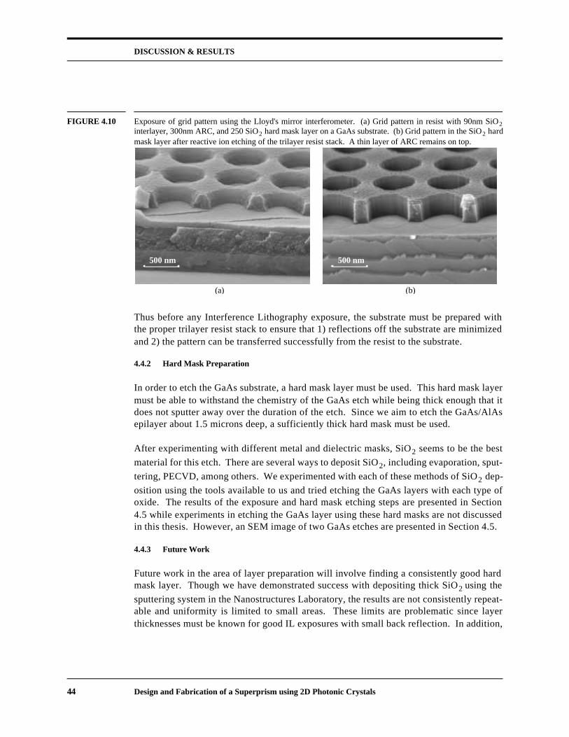
DISCUSSION & RESULTS
44 Design and Fabrication of a Superprism using 2D Photonic Crystals
FIGURE 4.10 Exposure of grid pattern using the Lloyd's mirror interferometer. (a) Grid pattern in resist with 90nm SiO2interlayer, 300nm ARC, and 250 SiO2 hard mask layer on a GaAs substrate. (b) Grid pattern in the SiO2 hardmask layer after reactive ion etching of the trilayer resist stack. A thin layer of ARC remains on top.
Thus before any Interference Lithography exposure, the substrate must be prepared withthe proper trilayer resist stack to ensure that 1) reflections off the substrate are minimizedand 2) the pattern can be transferred successfully from the resist to the substrate.
4.4.2 Hard Mask Preparation
In order to etch the GaAs substrate, a hard mask layer must be used. This hard mask layermust be able to withstand the chemistry of the GaAs etch while being thick enough that itdoes not sputter away over the duration of the etch. Since we aim to etch the GaAs/AlAsepilayer about 1.5 microns deep, a sufficiently thick hard mask must be used.
After experimenting with different metal and dielectric masks, SiO2 seems to be the bestmaterial for this etch. There are several ways to deposit SiO2, including evaporation, sput-tering, PECVD, among others. We experimented with each of these methods of SiO2 dep-osition using the tools available to us and tried etching the GaAs layers with each type ofoxide. The results of the exposure and hard mask etching steps are presented in Section4.5 while experiments in etching the GaAs layer using these hard masks are not discussedin this thesis. However, an SEM image of two GaAs etches are presented in Section 4.5.
4.4.3 Future Work
Future work in the area of layer preparation will involve finding a consistently good hardmask layer. Though we have demonstrated success with depositing thick SiO2 using thesputtering system in the Nanostructures Laboratory, the results are not consistently repeat-able and uniformity is limited to small areas. These limits are problematic since layerthicknesses must be known for good IL exposures with small back reflection. In addition,
500 nm 500 nm
(a) (b)

DISCUSSION & RESULTS
Design and Fabrication of a Superprism using 2D Photonic Crystals 45
the surface area of our superprism device is quite large making thickness uniformity criti-cal.
We will investigate other sources of oxide deposition. In particular, we will also investi-gate the use of flowable oxide as a substitute for deposited oxide. Flowable oxide such asDow Corning’s HSQ have the additional advantage of acting as an e-beam resist. Thoughthis advantage is not directly applicable to the process steps outlined for this device, itmost certainly would be advantageous for future device applications.
4.5 Reactive Ion Etching Results
Reactive ion etching is used to transfer patterns exposed during lithography steps through interme-diary layers into the GaAs/AlAs epilayer. Reactive ion etching is a dry etching technique wherebyions accelerate towards the material and react with the surface. This etching method allows forhighly anisotropic etching with straight sidewalls.
4.5.1 Tri-layer and hard mask etching results
Once the pattern has been exposed in resist, a number of different etching steps are neces-sary to transfer this pattern into the epilayer. After the interference lithography exposure,the hole pattern must be transferred from the resist layer through the SiO2 interlayer, ARClayer, the SiO2 hard mask layer, and finally into the GaAs/AlAs epilayer.
FIGURE 4.11 SEM image after an Interference Lithography exposure using the Lloyd’s mirror interferometer. The 750 nmperiod hole pattern is in about 200 nm of positive resist with a 20 nm SiO2 interlayer, 200 nm ARC layer, and100 nm SiO2 hard mask layer on a GaAs substrate.
~200 nm Resist
~100 nm SiO2
~200 nm ARC
~20 nm SiO2
GaAs substrate

DISCUSSION & RESULTS
46 Design and Fabrication of a Superprism using 2D Photonic Crystals
Since different materials have varying etch chemistries, different gases are used to etcheach layer. SiO2 is etched using fluorine-containing gases such as CHF3 or CF4, the ARClayer is etched using He/O2, and the GaAs/AlAs epilayers are etched using BCl3. Eachetching step must performed in such a way that the mask layer is not etched simulta-neously.
The details of a pattern in resist before reactive ion etching is shown in Figure 4.11. Thispattern was exposed using the Lloyd’s mirror interferometer in PFI 88 positive resist. TheSiO2 interlayer and ARC layers were then etched as shown in Figure 4.12. The SiO2 wasetched using CHF3 at 10 mT, 100V, 190W for 1 min, 10 sec. CHF3 does not etch poly-mers such as resist and is therefore a suitable gas for this step. The ARC layer was thenetched using a 2:1 mix of He and O2 at 10 mT, 250 V, 330 W, for 1 min, 40 sec.
FIGURE 4.12 SEM image showing holes in SiO2 and ARC. The SiO2 hard mask layer remains unetched. The 20 nm SiO2interlayer was etched using CHF3(10 mT, 100V, 190W, 1:10) and the 200 nm ARC layer was etched usingHe/O2(2:1 sccm, 10 mT, 250 V, 330 W, 1:40).
The SiO2 hard mask was then etched using CF4 as shown in Figure 4.13. CF4 etchespolymers such as ARC. However, since the ARC is twice as thick as the SiO2, it will notcompletely etch away before the SiO2 is etched even though the etch rate is faster. Thoughthe etch in Figure 4.13 is not complete, it still provides us useful information by allowingus to calculate etch rates of each material. The etch rates of SiO2 and ARC are about 30nm/min and 40 nm/min respectively. Therefore the complete etch of the hard mask can becompleted with the ARC mask in tact as long as the ARC is sufficiently thick.
~100 nm SiO2
~200 nm ARC
~20 nm SiO2
GaAs substrate
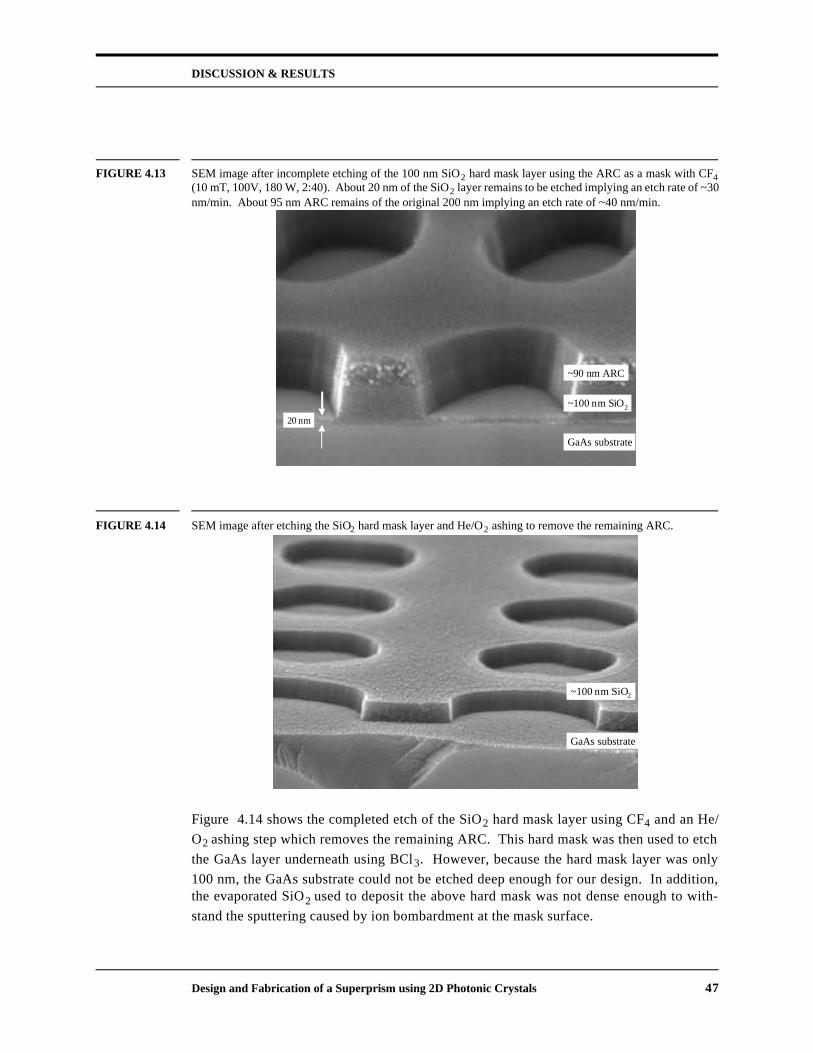
DISCUSSION & RESULTS
Design and Fabrication of a Superprism using 2D Photonic Crystals 47
FIGURE 4.13 SEM image after incomplete etching of the 100 nm SiO2 hard mask layer using the ARC as a mask with CF4(10 mT, 100V, 180 W, 2:40). About 20 nm of the SiO2 layer remains to be etched implying an etch rate of ~30nm/min. About 95 nm ARC remains of the original 200 nm implying an etch rate of ~40 nm/min.
FIGURE 4.14 SEM image after etching the SiO2 hard mask layer and He/O2 ashing to remove the remaining ARC.
Figure 4.14 shows the completed etch of the SiO2 hard mask layer using CF4 and an He/O2 ashing step which removes the remaining ARC. This hard mask was then used to etchthe GaAs layer underneath using BCl3. However, because the hard mask layer was only100 nm, the GaAs substrate could not be etched deep enough for our design. In addition,the evaporated SiO2 used to deposit the above hard mask was not dense enough to with-stand the sputtering caused by ion bombardment at the mask surface.
~100 nm SiO2
~90 nm ARC
GaAs substrate
20 nm
~100 nm SiO2
GaAs substrate

DISCUSSION & RESULTS
48 Design and Fabrication of a Superprism using 2D Photonic Crystals
We therefore tried a much thicker 500 nm SiO2 hard mask layer which was depositedusing a PECVD (Plasma Enhanced Chemical Vapor Deposition). Using a thicker hardmask layer necessitates using a thicker ARC and thicker SiO2 interlayer in order to trans-fer the hole pattern through each layer. A detail of the thicker tri-layer resist stack andhard mask layer is shown in Figure 4.15.
FIGURE 4.15 Detail of a Lloyd’s mirror exposure with trilayer resist stack and SiO2 hard mask layer on a GaAs substrate.
Though etching the tri-layer resist stack was straightforward, etching the SiO2 hard masklayer demonstrated the difference between etching with CF4 and CHF3. Since ARCetches at a rate of 40 nm/min using CF4, the mask would not be able to survive the 30 nm/min etching of the thicker SiO2. As an initial trial, we first tried a 1:1 CF 4/CHF3 mix tolower the etch rate of the ARC. The result is shown in Figure 4.16.
~300nm ARC
~500nm SiO2
~100nm SiO2
~200nm Resist
500 nmPeriod ~=750nmPFI-88 positive resist
Lloyd’s Mirror Exposure
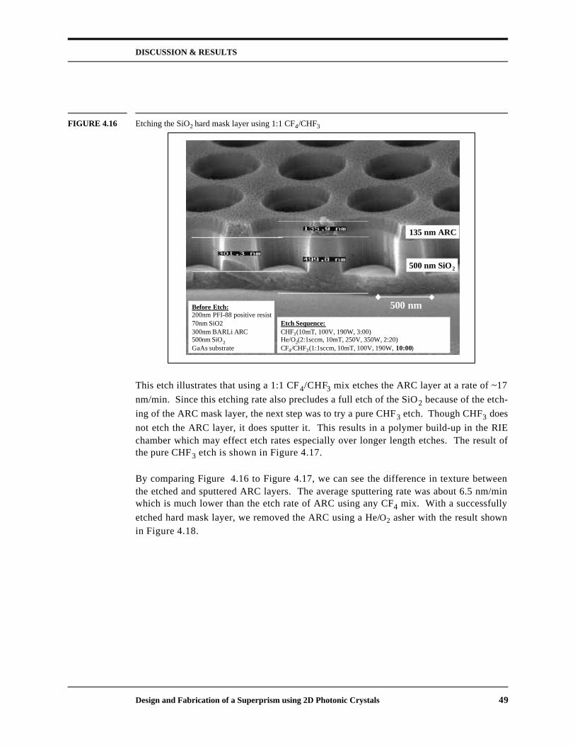
DISCUSSION & RESULTS
Design and Fabrication of a Superprism using 2D Photonic Crystals 49
FIGURE 4.16 Etching the SiO2 hard mask layer using 1:1 CF4/CHF3
This etch illustrates that using a 1:1 CF4/CHF3 mix etches the ARC layer at a rate of ~17nm/min. Since this etching rate also precludes a full etch of the SiO2 because of the etch-ing of the ARC mask layer, the next step was to try a pure CHF3 etch. Though CHF3 doesnot etch the ARC layer, it does sputter it. This results in a polymer build-up in the RIEchamber which may effect etch rates especially over longer length etches. The result ofthe pure CHF3 etch is shown in Figure 4.17.
By comparing Figure 4.16 to Figure 4.17, we can see the difference in texture betweenthe etched and sputtered ARC layers. The average sputtering rate was about 6.5 nm/minwhich is much lower than the etch rate of ARC using any CF4 mix. With a successfullyetched hard mask layer, we removed the ARC using a He/O2 asher with the result shownin Figure 4.18.
Etch Sequence:CHF3(10mT, 100V, 190W, 3:00)He/O2(2:1sccm, 10mT, 250V, 350W, 2:20)CF4/CHF3(1:1sccm, 10mT, 100V, 190W, 10:00)
Before Etch:300nm BARLi ARC500nm SiO2GaAs substrate
Before Etch:200nm PFI-88 positive resist70nm SiO2300nm BARLi ARC500nm SiO2GaAs substrate
500 nm SiO2
135 nm ARC
500 nm

DISCUSSION & RESULTS
50 Design and Fabrication of a Superprism using 2D Photonic Crystals
FIGURE 4.17 Etching of the SiO2 hard mask layer using CHF3.
FIGURE 4.18 A 500nm SiO2 hard mask layer after He/O2 ashing the ARC layer
Etch Sequence:CHF3(10mT, 100V, 190W, 3:00)He/O2(2:1sccm, 10mT, 250V, 350W, 2:20)CHF3(10mT, 100V, 190W, 19:00)
Before Etch:200nm PFI-88 positive resist70nm SiO2300nm BARLi ARC500nm SiO2GaAs substrate Sheila Tandon 11/20/01
Sheila Tandon 12/07/01
Etch Sequence:CHF3(10mT, 100V, 190W, 3:00)He/O2(2:1sccm, 10mT, 250V, 350W, 2:20)CHF3(10mT, 100V, 190W, 19:00)He/O2 Ashed 12:00
Before Etch:200nm PFI-88 positive resist70nm SiO2300nm BARLi ARC500nm SiO2GaAs substrate
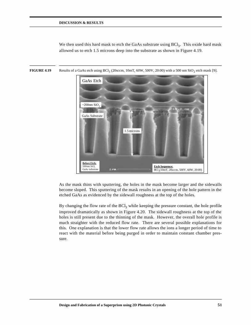
DISCUSSION & RESULTS
Design and Fabrication of a Superprism using 2D Photonic Crystals 51
We then used this hard mask to etch the GaAs substrate using BCl3. This oxide hard maskallowed us to etch 1.5 microns deep into the substrate as shown in Figure 4.19.
FIGURE 4.19 Results of a GaAs etch using BCl3 (20sccm, 10mT, 60W, 500V, 20:00) with a 500 nm SiO2 etch mask [9].
As the mask thins with sputtering, the holes in the mask become larger and the sidewallsbecome sloped. This sputtering of the mask results in an opening of the hole pattern in theetched GaAs as evidenced by the sidewall roughness at the top of the holes.
By changing the flow rate of the BCl3 while keeping the pressure constant, the hole profileimproved dramatically as shown in Figure 4.20. The sidewall roughness at the top of theholes is still present due to the thinning of the mask. However, the overall hole profile ismuch straighter with the reduced flow rate. There are several possible explanations forthis. One explanation is that the lower flow rate allows the ions a longer period of time toreact with the material before being purged in order to maintain constant chamber pres-sure.
Etch Sequence:BCl3(10mT, 20sccm, 500V, 60W, 20:00)
GaAs Etch
GaAs Substrate
~200nm SiO2
1.5 microns
Before Etch:500nm SiO2GaAs substrate
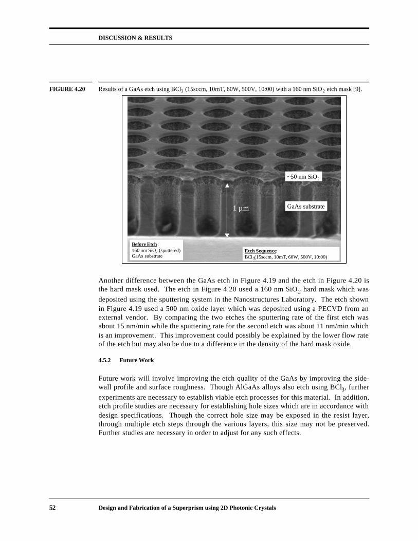
DISCUSSION & RESULTS
52 Design and Fabrication of a Superprism using 2D Photonic Crystals
FIGURE 4.20 Results of a GaAs etch using BCl3 (15sccm, 10mT, 60W, 500V, 10:00) with a 160 nm SiO2 etch mask [9].
Another difference between the GaAs etch in Figure 4.19 and the etch in Figure 4.20 isthe hard mask used. The etch in Figure 4.20 used a 160 nm SiO2 hard mask which wasdeposited using the sputtering system in the Nanostructures Laboratory. The etch shownin Figure 4.19 used a 500 nm oxide layer which was deposited using a PECVD from anexternal vendor. By comparing the two etches the sputtering rate of the first etch wasabout 15 nm/min while the sputtering rate for the second etch was about 11 nm/min whichis an improvement. This improvement could possibly be explained by the lower flow rateof the etch but may also be due to a difference in the density of the hard mask oxide.
4.5.2 Future Work
Future work will involve improving the etch quality of the GaAs by improving the side-wall profile and surface roughness. Though AlGaAs alloys also etch using BCl3, furtherexperiments are necessary to establish viable etch processes for this material. In addition,etch profile studies are necessary for establishing hole sizes which are in accordance withdesign specifications. Though the correct hole size may be exposed in the resist layer,through multiple etch steps through the various layers, this size may not be preserved.Further studies are necessary in order to adjust for any such effects.
~50 nm SiO2
GaAs substrate1 µm
Before Etch :160 nm SiO2 (sputtered)GaAs substrate
Etch Sequence:BCl3(15sccm, 10mT, 60W, 500V, 10:00)

DISCUSSION & RESULTS
Design and Fabrication of a Superprism using 2D Photonic Crystals 53
4.6 Oxidation Results
In order to confine light in the GaAs layer of the superprism, we need to surround this layer by lowrefractive index material. In our superprism design, the top face of the GaAs layer borders airwhile the lower face borders an aluminum oxide layer. This aluminum oxide layer is createdthrough the oxidation of an epitaxially grown AlxGa1-xAs layer.
4.6.1 Oxidation Experiments
The process used is a wet oxidation process identical to the one used in [10] for large scaleoxidation of AlAs films. Located in an elevated temperature furnace, as shown in Figure4.21, the film is exposed to water vapor which is carried into the furnace by an inert gassuch as N2. The temperature of the furnace is typically set between 350 and 500ºC. Therate at which the film is oxidized depends on a number of variables such as the tempera-ture of the furnace, the aluminum content of the film, the film's thickness, and the lateraldistance required for full oxidation.
FIGURE 4.21 Oxidation setup showing quartz tube which carries water vapor and N2 into an elevated temperature furnace.
Since we are operating at a wavelength of about 3µm, our superprism design requires alow index oxide layer with a thickness of about 3µm. The longest lateral distance requiredfor the oxidation front would be about 3mm, which is half the longest distance betweenthe device edge and the edge of the photonic crystal square area (see Figure 4.22). Sincethe photonic crystal area is dominated by air holes etched deeper than the top GaAs layer,the water vapor can penetrate the exposed AlGaAs layer from this direction as well asfrom the input and output edges of the device.
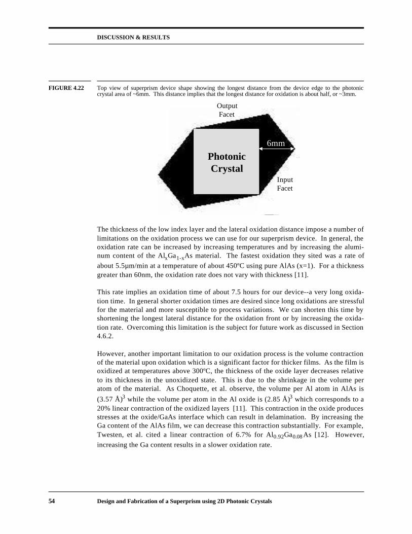
DISCUSSION & RESULTS
54 Design and Fabrication of a Superprism using 2D Photonic Crystals
FIGURE 4.22 Top view of superprism device shape showing the longest distance from the device edge to the photoniccrystal area of ~6mm. This distance implies that the longest distance for oxidation is about half, or ~3mm.
The thickness of the low index layer and the lateral oxidation distance impose a number oflimitations on the oxidation process we can use for our superprism device. In general, theoxidation rate can be increased by increasing temperatures and by increasing the alumi-num content of the AlxGa1-xAs material. The fastest oxidation they sited was a rate ofabout 5.5µm/min at a temperature of about 450ºC using pure AlAs (x=1). For a thicknessgreater than 60nm, the oxidation rate does not vary with thickness [11].
This rate implies an oxidation time of about 7.5 hours for our device--a very long oxida-tion time. In general shorter oxidation times are desired since long oxidations are stressfulfor the material and more susceptible to process variations. We can shorten this time byshortening the longest lateral distance for the oxidation front or by increasing the oxida-tion rate. Overcoming this limitation is the subject for future work as discussed in Section4.6.2.
However, another important limitation to our oxidation process is the volume contractionof the material upon oxidation which is a significant factor for thicker films. As the film isoxidized at temperatures above 300ºC, the thickness of the oxide layer decreases relativeto its thickness in the unoxidized state. This is due to the shrinkage in the volume peratom of the material. As Choquette, et al. observe, the volume per Al atom in AlAs is(3.57 Å)3 while the volume per atom in the Al oxide is (2.85 Å)3 which corresponds to a20% linear contraction of the oxidized layers [11]. This contraction in the oxide producesstresses at the oxide/GaAs interface which can result in delamination. By increasing theGa content of the AlAs film, we can decrease this contraction substantially. For example,Twesten, et al. cited a linear contraction of 6.7% for Al0.92Ga0.08 As [12]. However,increasing the Ga content results in a slower oxidation rate.
6mm
PhotonicCrystal
OutputFacet
InputFacet
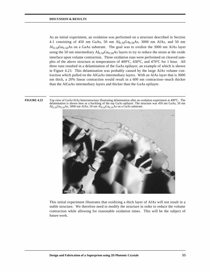
DISCUSSION & RESULTS
Design and Fabrication of a Superprism using 2D Photonic Crystals 55
As an initial experiment, an oxidation was performed on a structure described in Section4.1 consisting of 450 nm GaAs, 50 nm Al0.50Ga0.50As, 3000 nm AlAs, and 50 nmAl0.50Ga0.50As on a GaAs substrate. The goal was to oxidize the 3000 nm AlAs layerusing the 50 nm intermediary Al0.50Ga0.50As layers to try to reduce the strain at the oxideinterface upon volume contraction. Three oxidation runs were performed on cleaved sam-ples of the above structure at temperatures of 400ºC, 430ºC, and 470ºC for 1 hour. Allthree runs resulted in a delamination of the GaAs epilayer, an example of which is shownin Figure 4.23. This delamination was probably caused by the large AlAs volume con-traction which pulled on the AlGaAs intermediary layers. With an AlAs layer that is 3000nm thick, a 20% linear contraction would result in a 600 nm contraction--much thickerthan the AlGaAs intermediary layers and thicker than the GaAs epilayer.
FIGURE 4.23 Top view of GaAs/AlAs heterostructure illustrating delamination after an oxidation experiment at 400ºC. Thedelamination is shown here as a buckling of the top GaAs epilayer. The structure was 450 nm GaAs, 50 nmAl0.50Ga0.50As, 3000 nm AlAs, 50 nm Al0.50Ga0.50As on a GaAs substrate.
This initial experiment illustrates that oxidizing a thick layer of AlAs will not result in astable structure. We therefore need to modify the structure in order to reduce the volumecontraction while allowing for reasonable oxidation times. This will be the subject offuture work.
DISCUSSION & RESULTS
56 Design and Fabrication of a Superprism using 2D Photonic Crystals
4.6.2 Future Work
Future work on the oxidation of the superprism epilayer will involve finding a materialthat will allow for reasonable oxidation times while maintaining stable layer interfaces.There are a number of approaches we can experiment with.
By grading the Al content of the interface layer continuously from GaAs to AlAs we canreduce the stress at the AlAs/GaAs interface through a thin oxide transition layer. Thistype of transition layer is straightforward to grow epitaxially. However, even with thistransition layer, the volume contraction of such a thick AlAs layer may again result indelamination.
We can shorten the total oxidation time by shortening the longest lateral distance for theoxidation front. This can be accomplished by introducing small holes in the GaAs epil-ayer which are etched into the AlAs layer and therefore expose this layer to the oxidationgas. The size of these holes would have to be large enough to allow for oxidation whilesmall enough, and with a period large enough, to neglect any scattering effects duringoperation of the device. The effect of this solution on device operation will have to beinvestigated through testing of the device. Initial oxidation experiments with such holescould use 1 µm diameter holes spaced with a period of ~700 µm. These holes can be pat-terned using mask 1 during the photolithography step.
Using a lower Al content film would allow us to lower the effect of volume contraction onthe heterostructure. Though this will result in lower oxidation rates, by using the largeperiod of small holes in the GaAs layer, we may be able to lower the total lateral oxidationdistance and therefore lower total oxidation times.
Another approach may be to use alternating thin layers of AlAs and AlGaAs to create a3µm thick layer for oxidation. The purpose of this layered structure would be to combinethe fast oxidation rates of AlAs with the stability of the interfaces between AlAs andAlGaAs while lowering the effect of volume contraction. The quickly oxidizing AlAs lay-ers would allow for oxidation of the AlGaAs layers from the top and bottom surfaces inaddition to oxidation in the lateral direction. Upon oxidation, the AlAs layers will experi-ence a greater contraction than the AlGaAs layers. This averages out to a lower overallcontraction in this structure relative to the pure AlAs case. A disadvantage of this alterna-tive would be the difficulty in the epitaxial growth.

CONCLUSION
Design and Fabrication of a Superprism using 2D Photonic Crystals 57
5.0 CONCLUSION
A superprism is an optical device which enhances the effects of a conventional prism intwo ways: it disperses multiple wavelengths of light over wide angles and it allows forhighly sensitive steering of a single wavelength beam.
In this Master's Thesis, a superprism device was designed focussing on realizing ultra-refraction of a single wavelength beam. A fabrication approach was then outlined, and allprocessing steps were investigated. Through simulations, we demonstrated that we canuse the phase velocity sensitivity in a photonic crystal to amplify a beam’s direction from+/- 2 degrees at the input to +/- 30 degrees at the output for a wavelength of 3 µm. Thisdesign differs from previous work in that these superprism effects are observable in airusing a simple 2D structure.
The 2D photonic crystal consists of a square lattice of air holes in GaAs surrounded by airon the top surface and low index aluminum oxide on the lower surface. The low indexoxide is fabricated through a wet oxidation of an epitaxially-grown AlGaAs layer.Because of the large surface area of the device, the photonic crystal grid is patterned usinginterference lithography with device facets defined using photolithography. All patternsare transferred into the GaAs/AlGaAs epilayers using reactive ion etching.
Progress on all fabrication steps of the superprism has been demonstrated and theapproach for future work has been identified. At the present, only minor adjustments arenecessary for most fabrication steps. Successful fabrication of the device is most criticallylimited by the large scale oxidation necessary to create the thick low index layer. How-ever, the direction of future experiments on this process have been outlined.
REFERENCES
58 Design and Fabrication of a Superprism using 2D Photonic Crystals
6.0 REFERENCES
[1] H. Kosaka, T. Kawashima, A. Tomita, M. Notomi, T. Tamamura, T. Sato, and S. Kawakami. "Superprism Phenomena in Photonic Crystals: Toward Microscale Lightwave Circuits." J. of Lightwave Technology, Vol. 17, No. 11, pp. 2032-2038, (1999).
[2] H. Kosaka, T. Kawashima, A. Tomita, M. Notomi, T. Tamamura, T. Sato, and S. Kawakami. "Self-collimating phenomena in photonic crystals." Applied Physics Letters , Vol. 74, No. 9, pp. 1212-1214, (1999).
[3] B. E. Nelson, M. Gerken, D. A. Miller, and R. Piestun. "Use of a dielectric stack as a one-dimensional photonic crystal for wavelength demultiplexing by beam shifting." Optics Letters, Vol. 25, No. 20, pp. 1502-1504, (2000).
[4] J. A. Kong. Electromagnetic Wave Theory. EMW Publishing, 2000. pp. 335-345.
[5] J. Joannopoulos, R. Meade, J. Winn. Photonic Crystals: Molding the Flow of Light. Princeton University Press, 1995, Chapters 1-4.
[6] S. G. Johnson and J. D. Joannopoulos, "Block-iterative frequency-domain methods for Maxwell's equations in a planewave basis," Optics Express , Vol. 8, No. 3, 173-190 (2001).
[7] Simulations performed by Chiyan Luo, MIT. Figures adapted and used with permission.
[8] Michael E. Walsh. “Nanostructuring Magnetic Thin Films Using Interference Lithography.” M.S. Thesis, MIT (2000).
[9] Solomon Assefa, MIT. Figure used with permission.
[10] Alexei E. Erchak. “Enhanced Performance of Optical Sources in III-V Materials Using Photonic Crystals.” Ph.D. Thesis, MIT (2002).
[11] K. D. Choquette, K. M. Geib, C. Ashby, et al. “Advances in Selective Wet Oxidation of AlGaAs Alloys.” IEEE Journal of Selected Topics in Quantum Electronics, Vol. 3, No. 3, 916-926, (1997).
[12] R. D. Twesten, D. M. Follstaedt, K. D. Choquette, et al. “Microstructure of laterally oxidized AlxGa1-xAs layers in vertical cavity lasers,” Applied Physics Letters, Vol. 69, 19-21, (1996).
[13] W. T. Tsang, M. Olmstead, and R. P. H. Chang. “Multidielectrics for GaAs MIS devices using composition-grades AlxGa1-xAs and oxidized AlAs.” Applied Physics Letters, 34 (6), 408-410, (1979).


![Observation of wavelength-dependent Brewster angle shift in 3D photonic crystals … · 2016-11-30 · 3 crystal due to its ease of fabrication and affordability [21 ]. Such 3D photonic](https://img.pdfslide.us/doc/110x75/5f7217247e7c6e38586ba65a/observation-of-wavelength-dependent-brewster-angle-shift-in-3d-photonic-crystals.jpg)