Embed Size (px)
Citation preview

NRL/MR/5317--20-10,130
Design and Development of Butler Matrices for Circular Array BeamformingRashmi MitalWilliam R. PicklesMark G. Parent
Radar Analysis BranchRadar Division
September 22, 2020
DISTRIBUTION STATEMENT A: Approved for public release, distribution is unlimited.
Naval Research Laboratory Washington, DC 20375-5320
UNCLASSIFIED//DISTRIBUTION A

i
REPORT DOCUMENTATION PAGE Form ApprovedOMB No. 0704-0188
3. DATES COVERED (From - To)
Standard Form 298 (Rev. 8-98)Prescribed by ANSI Std. Z39.18
Public reporting burden for this collection of information is estimated to average 1 hour per response, including the time for reviewing instructions, searching existing data sources, gathering and maintaining the data needed, and completing and reviewing this collection of information. Send comments regarding this burden estimate or any other aspect of this collection of information, including suggestions for reducing this burden to Department of Defense, Washington Headquarters Services, Directorate for Information Operations and Reports (0704-0188), 1215 Jefferson Davis Highway, Suite 1204, Arlington, VA 22202-4302. Respondents should be aware that notwithstanding any other provision of law, no person shall be subject to any penalty for failing to comply with a collection of information if it does not display a currently valid OMB control number. PLEASE DO NOT RETURN YOUR FORM TO THE ABOVE ADDRESS.
5a. CONTRACT NUMBER
5b. GRANT NUMBER
5c. PROGRAM ELEMENT NUMBER
5d. PROJECT NUMBER
5e. TASK NUMBER EW-271-0015f. WORK UNIT NUMBER
2. REPORT TYPE1. REPORT DATE (DD-MM-YYYY)
4. TITLE AND SUBTITLE
6. AUTHOR(S)
8. PERFORMING ORGANIZATION REPORTNUMBER
7. PERFORMING ORGANIZATION NAME(S) AND ADDRESS(ES)
10. SPONSOR / MONITOR’S ACRONYM(S)9. SPONSORING / MONITORING AGENCY NAME(S) AND ADDRESS(ES)
11. SPONSOR / MONITOR’S REPORTNUMBER(S)
12. DISTRIBUTION / AVAILABILITY STATEMENT
13. SUPPLEMENTARY NOTES
14. ABSTRACT
15. SUBJECT TERMS
16. SECURITY CLASSIFICATION OF:
a. REPORT
19a. NAME OF RESPONSIBLE PERSON
19b. TELEPHONE NUMBER (include areacode)
b. ABSTRACT c. THIS PAGE
18. NUMBEROF PAGES
17. LIMITATIONOF ABSTRACT
Design and Development of Butler Matrices for Circular Array Beamforming
Rashmi Mital, William, R. Pickles, and Mark P. Parent
Naval Research Laboratory4555 Overlook Avenue, SWWashington, DC 20375-5320
NRL/MR/5317--20-10,130
ONR
DISTRIBUTION STATEMENT A: Approved for public release; distribution is unlimited.
UnclassifiedUnlimited
UnclassifiedUnlimited
UnclassifiedUnlimited
28
Rashmi Mital
(202) 767-2584
Antennas that have elements placed in a circular fashion require complex beamforming strategies as each element has a different pointingdirection and thus the overall radiation pattern cannot be simplified as for planar arrays. However by transforming the circular elements into phasemodes using a passive Butler matrix we can create elements that now behave similar to elements in a planar array. In this report we describehow to design these wideband Butler matrices using fixed-value differential phase shifters with microstrip techniques. The details of the designand simulated performance are presented for a complete 4 X 4 and a 8 X 8 Butler matrix.
22-09-2020 NRL Memorandum Report
6B48
Office of Naval ResearchOne Liberty Center875 N Randolph Street, Suite 1425Arlington, VA 22203-1995
62271N
Dec 19 – Jun 20
UnclassifiedUnlimited
UNCLASSIFIED//DISTRIBUTION A

This page intentionally left blank.
ii

iii | P a g e
CONTENTS
1. Introduction ........................................................................................................................................................... 3
2. Wideband Phase SHifters ...................................................................................................................................... 5
2.1 Shiffman Phase Shifter ................................................................................................................................. 5
2.1.1 Designing a Shiffman Phase Shifter ......................................................................................................... 6
2.2 Designing a Shiffman Phase Shifter in Microstrip ........................................................................................ 9
2.3 Building a 𝟒 × 𝟒 Butler Matrix ................................................................................................................... 15
3. Final Design .......................................................................................................................................................... 16
3.1 4-element Butler Matrix ............................................................................................................................. 16
3.2 The 𝟖 × 𝟖 Butler Matrix ............................................................................................................................. 20
3.2.1 Design of 45deg phase shifter ............................................................................................................... 20
3.2.2 Cross-over design for 8-inputs ............................................................................................................... 22
4. Conclusion ........................................................................................................................................................... 25
5. References ........................................................................................................................................................... 26

iv | P a g e
LIST OF FIGURES
Figure 1: Examples of phase variation of phase modes of a circular array vs. radiation angle ..................................... 4
Figure 2: Forming phase modes from circular array elements ...................................................................................... 4
Figure 3: An example of a single stage Shiffman phase shifter ..................................................................................... 6
Figure 4: Standard Shiffman phase shifter with a typical phase response [after Ref [9]] ............................................. 7
Figure 5: An example to relate min/max frequency to phase deviation ....................................................................... 8
Figure 6: A starting design of wideband Shiffman Phase Shifter ................................................................................... 9
Figure 7: Design and performance for an ideal microstrip design............................................................................... 10
Figure 8: Electrical and layout of Shiffman Phase Shifter ............................................................................................ 10
Figure 9: Comparing theoretical and practical phase shifter design performance ..................................................... 11
Figure 10: HFSS layout of the 90deg Shiffman phase shifter ....................................................................................... 12
Figure 11: (a) Phase performance (b) insertion loss (c) reflection loss and (d) impedance of designed Shiffman Phase
shifter........................................................................................................................................................................... 13
Figure 12: Layout of a 0deg phase shifter ................................................................................................................... 13
Figure 13: (a) Phase performance and (b) Insertion loss and reflection loss across band of operation ..................... 14
Figure 14: Layout of 𝟒 × 𝟒 Butler matrix using designed 0deg and 90deg phase shifters .......................................... 15
Figure 15: Phase performance from input port 2 to each of the output ports (5 to 8) ............................................... 15
Figure 16: 90deg phase shifter .................................................................................................................................... 16
Figure 17: (a) Phase performance of 90deg phase shifter (b) insertion loss across the band and (c) reflection loss of
the differential phase shifter ....................................................................................................................................... 17
Figure 18: Layout of the 0deg phase shifter ................................................................................................................ 18
Figure 19: Layout of cross-over for 𝟒 × 𝟒 Butler matrix ............................................................................................. 18
Figure 20: Performance of the cross-over across the band of interest ....................................................................... 19
Figure 21: Complete layout of 𝟒 × 𝟒 Butler matrix ..................................................................................................... 20
Figure 22: Layout and dimensioning of 45deg phase shifter ....................................................................................... 21
Figure 23: (a) Reflection performance (b) Insertion loss and (c) phase performance of the device shown in Fig. 21 22
Figure 24: Cross-over design for the 𝟖 × 𝟖 Butler matrix ........................................................................................... 23
Figure 25: (a) Reflection loss and (b) delay for the various paths of cross-over ......................................................... 24
Figure 26: Final layout for the 𝟖 × 𝟖 Butler Matrix ..................................................................................................... 24

1 | P a g e
Design and Development of Butler Matrices for Circular Array Beamforming
R. Mital, W. R. Pickles and M. G. Parent
Radar Analysis Branch, Radar Division
1. INTRODUCTION
Antennas that have elements placed in a circular fashion have been studied but have not in the past gotten as much
use as planar arrays. Cylindrical phased arrays satisfy many of the stringent requirements that are placed on
multifunction apertures with their ability to offer a full 360o view using omnidirectional or directional modes.
Cylindrical arrays also do not require handoff between the multiple faces as is needed for planar arrays. Furthermore,
cylindrical arrays have several advantages compared to multi-face planar arrays. One, the beam does not suffer from
scan loss or beam broadening in the azimuthal direction. This means that the array does not have to be increased in
size to maintain gain at larger scan angles. Secondly cylindrical arrays are able to form omnidirectional or sector
beams without additional complexity.
A cylindrical array can theoretically be separated into a product of a linear array and a circular array, just as a planar
array can be thought of as being made of two orthogonal linear arrays. With this simplification, it is possible to
analyze the cylindrical array by analyzing the linear array and circular array separately. In this array we will only look
at the circular array with the understanding that beamforming techniques for linear arrays are quite mature and
well-known.
Scanning a beam from a circular array is more involved compared to planar arrays. The reason can be attributed to
the fact that the element pattern of each element in a circular array is different as each element in this array points
in a different direction. This means that each element’s contribution toward a directional beam formation is not the
same for the different scan angles. On the other hand, in a planar array, element points in the same direction,
allowing the simplification in the radiation pattern calculation to a product of array factor and the element factor.
As discussed [1, 2], one way of simplifying circular beamforming is to form phase modes by combining all the
elements of the circular array. Each phase modes has unit amplitude and phase that cycles between 0 and 2𝜋, with
the number of cycles depending on the mode number – see Figure 1. Each phase mode has a radiation pattern of
𝑒𝑗𝑀𝜙 where 𝑀 indicates the phase mode number. In Figure 1, the phase of three of these modes is shown. The
amplitude of each of these phase modes stays constant at unity. Mode 1 cycles once between 0 and 2𝜋 while Mode
______________Manuscript approved September 17, 2020.

2 | P a g e
2 cycles twice. To form a scanning directional beam, these phase modes can be weighted, phased and summed
together [2]. Thus phase modes can be thought of as analogous to elements of a linear array and phase mode
beamforming can use the mature and well-known beamforming techniques of linear array beamforming.
Figure 1: Examples of phase variation of phase modes of a circular array vs. radiation angle
One way to form phase modes is to use Butler matrices [2]. These can be designed to have 𝑁 inputs and 𝑁 outputs.
The 𝑁 inputs are the inputs of the circular array while the outputs will be each of the phase modes. This
transformation is shown in Figure 2. Butler matrix uses hybrid couplers and fixed-values phase shifters. Details of
how to determine the phase values of the fixed-value phase shifters was discussed in detail in Ref. [1] using equations
found in [3]. In this report, we will discuss the methodology of designing and building the fixed-value phase shifters
using microstrip techniques.
Figure 2: Forming phase modes from circular array elements
In a Butler matrix design, the phase shifter normally has a limited bandwidth performance. Research is on-going to
design phase shifters that are wideband especially using microstrip techniques [4, 5, 6, 7, 8]. The objective of our
work here in this program is not to design ultra-wideband Butler matrices but rather to use these phase shifters to
Butler Matrix
Phase Modes
Circular Elements

3 | P a g e
form passive Butler matrices that can be used to form phase modes. We will follow a simple coupled line
methodology design phase shifters over a band of 2 – 5 GHz and use these to design the required Butler matrix
designs. As a part of this report, we will discuss the steps to design a 4 × 4 and 8 × 8 Butler matrix, as well as the
steps to design simple Shiffman phase shifters.
2. WIDEBAND PHASE SHIFTERS
As we know, phase shifters are extremely common microwave devices that are widely used in electronic beam
steered phased arrays, microwave instrumentation and modulators among others applications. A lot of work is being
done to design and develop wideband phase shifters. A detailed discussion of these devices can be found in literature
[9, 10, 11]. Shiffman phase shifters are common and easy to design and build. Compared to other coupled designs
[7, 9], these may have smaller bandwidths of operation, but the ease of modeling and building make them ideal for
our effort here. For the design methodology, we will discuss the steps taken to design the Shiffman phase shifter
[12].
2.1 Shiffman Phase Shifter
The Shiffman phase shifter is a differential phase shifter that consists of two transmission lines, one of which is a
coupled transmission line. By properly selecting the length of the two lines as well as the degree of coupling, it is
possible to obtain a flat phase shift over a relatively broad bandwidth. Shiffman’s original designs used the stripline
structures where the odd and even mode propagating along the coupled lines have equal phase velocities. In the
presented design, we have decided to use microstrip structures instead of stripline structures, to simplify
manufacturing. However, using microstrip structures result in unequal even and odd velocities which causes reduced
coupling and narrows the bandwidth over which the constant phase shifts can be formed. To improve this
performance, it is possible to consider other wideband phase shifter designs found in literature [4, 6]. However these
were found to be not as mature and as designing a broad-band phase shifter is not the objective of this effort, we
decided to stay with the Shiffman phase shifter methodology.
Figure 2 shows an example of a simple Shiffman phase shifter using transmission lines. A quick overview of the steps
that were followed to design this phase shifter is provided in the next section.

4 | P a g e
Figure 3: An example of a single stage Shiffman phase shifter
To start the process of designing a wideband phase shifter, we followed Ref [9] to determine the steps needed to
design a 90o differential phase shifter. For this project, we need to design phase shifters to operate at a center
frequency of 3500 MHz.
2.1.1 Designing a Shiffman Phase Shifter
The differential phase shifter provides the desired phase by subtracting the phase response of the coupled section
with the phase response of the adjacent uniform line.
Δ𝜙 = 𝐾𝜃 − cos−1 (𝜌 − tan2 𝜃
𝜌 + tan2 𝜃)
(1)
In Eq. (1) 𝜃 is the electrical length of the coupled section and 𝜌 is its impedance ratio. The impedance ratio is defined
as
𝜌 =𝑍0𝑒
𝑍0𝑜
(2)
In Eq. (2) 𝑍0𝑒 and 𝑍0𝑜
are the even and odd impedances of the coupled section line respectively. For microstrip lines,
these two impedances are not the same but still meets the following requirement at all frequencies of operation
𝑍0 = √𝑍0𝑒× 𝑍0𝑜
.
.
(3)
The coupling factor 𝐶 and the impedance ratio can be related as shown below.
𝐶 = −20 × log10 (𝜌 − 1
𝜌 + 1)
(4)
An example of a Shiffman phase shifter response is shown in Fig. 4 below. The coupling factor and the odd and even
impedances can be varied to determine the error in the phase shift across the band of interest. Figure 4 relates
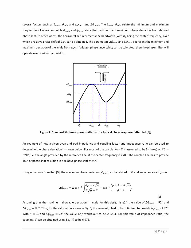
5| P a g e
several factors such as 𝜃𝑚𝑎𝑥 , 𝜃𝑚𝑖𝑛 and Δ𝜙𝑚𝑎𝑥 and Δ𝜙𝑚𝑖𝑛 . The 𝜃𝑚𝑎𝑥 , 𝜃𝑚𝑖𝑛 relate the minimum and maximum
frequencies of operation while 𝜙𝑚𝑎𝑥 and 𝜙𝑚𝑖𝑛 relate the maximum and minimum phase deviation from desired
phase shift. In other words, the horizontal axis represents the bandwidth (with 𝜃0 being the center frequency) over
which a relative phase shift of Δ𝜙0 can be obtained. The parameters Δ𝜙𝑚𝑖𝑛 and Δ𝜙𝑚𝑎𝑥 represent the minimum and
maximum deviation of the angle from Δ𝜙0. If a larger phase uncertainty can be tolerated, then the phase shifter will
operate over a wider bandwidth.
Figure 4: Standard Shiffman phase shifter with a typical phase response [after Ref [9]]
An example of how a given even and odd impedance and coupling factor and impedance ratio can be used to
determine the phase deviation is shown below. For most of the calculations 𝐾 is assumed to be 3 (three) or 𝐾𝜃 =
270𝑜, i.e. the angle provided by the reference line at the center frequency is 270o. The coupled line has to provide
180o of phase shift resulting in a relative phase shift of 90o.
Using equations from Ref. [9], the maximum phase deviation, 𝜙𝑚𝑎𝑥 can be related to 𝐾 and impedance ratio, 𝜌 as
Δ𝜙𝑚𝑎𝑥 = 𝐾 tan−1 √𝐾𝜌 − 2√𝜌
2√𝜌 − 𝐾− cos−1 (
𝜌 + 1 − 𝐾√𝜌
𝜌 − 1).
(5)
Assuming that the maximum allowable deviation in angle for this design is ±2o, the value of Δ𝜙𝑚𝑎𝑥 = 92𝑜 and
Δ𝜙𝑚𝑖𝑛 = 88𝑜. Thus, for the calculation shown in Fig. 5, the value of 𝜌 had to be optimized to provide Δ𝜙𝑚𝑎𝑥 of 92o.
With 𝐾 = 3 , and Δ𝜙𝑚𝑎𝑥 = 92𝑜 the value of 𝜌 works out to be 2.6233. For this value of impedance ratio, the
coupling, 𝐶 can be obtained using Eq. (4) to be 6.975.
qL qmax q0 qmin qR
Dfmin
Df0
Dfmax
Reference line
Relative Phase

6 | P a g e
Figure 5: An example to relate min/max frequency to phase deviation
The maximum phase deviation, 𝜖 can be related to minimum and maximum relative phase as
𝜖 = Δ𝜙𝑚𝑎𝑥 − Δ𝜙0 = Δ𝜙0 − Δ𝜙𝑚𝑖𝑛 .
(6)
Thus, the ratio of the lowest frequency of operation to center frequency (i.e. 𝜃𝐿) can be related to Δ𝜙𝑚𝑖𝑛 as shown
in Ref. [9].
Δ𝜙𝑚𝑖𝑛 = 𝐾𝜃𝐿 − cos−1 (𝜌 − tan2 𝜃𝐿
𝜌 + tan2 𝜃𝐿
)
(7)
Once again, the value of 𝜃𝐿 was optimized until the value of Δ𝜙𝑚𝑖𝑛 was close to the desired value of 88deg. This
worked out to be 62.896deg. The maximum and minimum of values of 𝜃 are related as
𝜃𝐿 = 180𝑜 − 𝜃𝑅.
(8)
Finally, the maximum bandwidth over which this phase shift can be obtained can be determined by
𝐵 = (𝜃𝑅 − 𝜃𝐿
𝜃0
).
(9)
In this example a 90o phase shifter with ±2o error will be designed with a 60% bandwidth. Using the equations
discussed earlier, this phase shifter will need a coupling of 6.975 dB from the coupled line and an impedance ratio
of 2.623. With these input the odd and even impedance were calculated to be 30.9Ω and 81.0Ω respectively. The
values for 𝜃𝑅 and 𝜃𝐿 were found to be 117.104o and 62.896o. Note, these equations are all independent of
frequencies. Once these parameters have been calculated, the microstrip lengths can be found based on the
electrical length and the desired frequency of operation. Using these equations, the next step was to actually design
a phase shift to provide 90deg phase shift at center frequency of 3500 MHz.
Input Impedance, ZI 50 W
Even Impedance, Ze 80.9784 W
Odd Impedance, Zo 30.8724 W
Impedance Ratio, r 2.623
Coupling, C 6.975 dB
K 3
Phase deviation. e 2 deg
Bandwidth 60.2311 %
qR 117.104 deg
qL 62.896 deg
q 90 deg
Df 90 deg
fmax 92 deg
fmin 88 deg

7| P a g e
2.2 Designing a Shiffman Phase Shifter in Microstrip
To design a phase shifter in microstrip, a combination of tools were utilized. To start off, we will present the steps
that were followed to develop the phase shifter. In the next section, we will present the final 4 × 4 and 8 × 8 Butler
matrix designs.
Initially, using the calculator shown in Fig. 5, a design for a 90o phase shifter was put together. An example of this is
shown in Fig. 6. This phase shifter is designed to have a phase deviation of less than 0.5o over an operating frequency
band of 3200MHz to 4200MHz. This is a bandwidth of 30%. If a higher bandwidth is desired than a larger angle
deviation will have to be accepted. The details of the design are shown in Figure 6a while the phase performance is
shown in Figure 6b.
(a)
(b)
Figure 6: A starting design of wideband Shiffman Phase Shifter
The next step is to convert the transmission line design into a microstrip line design. The TLINE function in the
GENESYS® tool can be used to do the initial conversion. Choosing the center frequency of 3500MHz the converted
microstrip design is shown in Fig. 7. For this conversion, the substrate chosen is Rodgers 4350 board which is 60mil
thick, with a dielectric constant of 3.48 and a loss tangent of 0.004. The performance for this ideal conversion is also
shown in Fig. 7. After this conversion, there is a good match in performance between the microstrip and ideal
designs.
LENGTH=843.643 mil
ZOO=33 Ω
ZOE=75.75 Ω
TL2
F=3500 MHz
PORT=3
VS3
Port_4
L=270 °
Z=50 Ω
TL1
F=3500 MHz
PORT=1
VS1
Port_2
8 | P a g e
(a) (b)
Figure 7: Design and performance for an ideal microstrip design
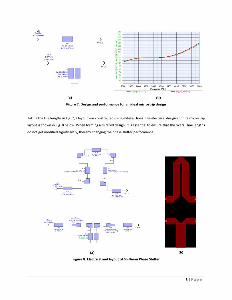
Taking the line lengths in Fig. 7, a layout was constructed using mitered lines. The electrical design and the microstrip
layout is shown in Fig. 8 below. When forming a mitered design, it is essential to ensure that the overall line lengths
do not get modified significantly, thereby changing the phase shifter performance
(a) (b)
Figure 8: Electrical and layout of Shiffman Phase Shifter
F=3500 MHz
PORT=1
VS1
Port_2
L=1518.756 mil
W=134.7 mil
TL1
Port_4
L=521.68 mil
S=9.648 mil
W=98.206 mil
TL2
F=3500 MHz
PORT=3
VS3
Frequency (MHz)
an
g(S
[4,3
]/S
[2,1
]),
an
g(S
[4,3
]/S
[2,1
]) (
de
g)
0
10
20
30
40
50
60
70
80
90
100
110
120
130
140
150
160
170
180
Frequency (MHz)
2000 2400 2800 3200 3600 4000 4400 4800 5200 5600 6000
ang(S[4,3]/S[2,1]) ang(S[4,3]/S[2,1])
Port_2
F=3500 MHzPORT=1
VS1
BN1
BN2
BN4
BN3 L=50 mil
W=134.7 milTL3
BN5
BN6
L=494.2 mil
S=9.648 milW=98.206 mil
TL2
L=100 mil
W=134.7 mil
TL8 Port_4
F=3500 MHz
PORT=3VS3
L=100 mil
W=134.7 mil
TL1
LEN=100 milW2=134.7 mil [W50]
W1=98.206 mil
TP1
LEN=100 mil
W2=134.7 mil [W50]
W1=98.206 mil
TP2
L=662.3 mil [55+ALen+BLen]W=134.7 mil
TL4
L=662.3 mil [55+ALen+BLen]W=134.7 mil
TL5
L=145 mil [200-55]
W=134.7 milTL6
L=145 mil [200-55]W=134.7 mil
TL7

9| P a g e
With the layout as shown in Fig. 8, the phase shifter performance across the band of interest is shown in Fig. 9. The
overall errors increase due to the use of mitered line, in the reference line, which results in increased coupling due
to the limited spacing between the lines. The parameter that still requires analysis or optimization is the width of
the microstrip line that connects the coupled line. In the current design, it is modeled as a short, however practically,
it is not possible to short this, so a finite width line will have to be utilized. The thicker this line is, the more the
degradation is seen in the overall performance.
Figure 9: Comparing theoretical and practical phase shifter design performance
To complete the design, we used High Frequency Structure Simulator (HFSS), a commercially available finite element
method solver for electromagnetic structure from Ansys, to optimize the design of the phase shifter. The use of this
software allows us to optimize the design for best possible performance.
Taking the preliminary design from Genesys, we exported the design into HFSS. This exported design is shown in Fig.
10. The “red” boxes in the figure indicate the location of Electromagnetic (EM) ports. With these ports in place, HFSS
is able to carry out a finite-element simulation of how EM fields radiate and couple between the two microstrip lines.
Frequency (MHz)
an
g(S
[4,3
]/S
[2,1
]),
an
g(S
[4,3
]/S
[2,1
]) (
de
g)
0
10
20
30
40
50
60
70
80
90
100
110
120
130
140
150
160
170
180
Frequency (MHz)
2000 2400 2800 3200 3600 4000 4400 4800 5200 5600 6000
ang(S[4,3]/S[2,1]) ang(S[4,3]/S[2,1])
10 | P a g e
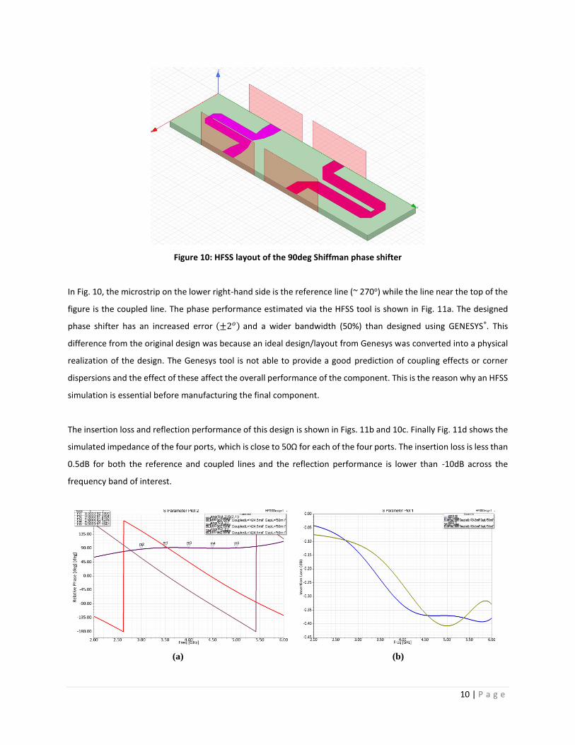
Figure 10: HFSS layout of the 90deg Shiffman phase shifter
In Fig. 10, the microstrip on the lower right-hand side is the reference line (~ 270o) while the line near the top of the
figure is the coupled line. The phase performance estimated via the HFSS tool is shown in Fig. 11a. The designed
phase shifter has an increased error (±2𝑜) and a wider bandwidth (50%) than designed using GENESYS®. This
difference from the original design was because an ideal design/layout from Genesys was converted into a physical
realization of the design. The Genesys tool is not able to provide a good prediction of coupling effects or corner
dispersions and the effect of these affect the overall performance of the component. This is the reason why an HFSS
simulation is essential before manufacturing the final component.
The insertion loss and reflection performance of this design is shown in Figs. 11b and 10c. Finally Fig. 11d shows the
simulated impedance of the four ports, which is close to 50Ω for each of the four ports. The insertion loss is less than
0.5dB for both the reference and coupled lines and the reflection performance is lower than -10dB across the
frequency band of interest.
(a) (b)

11 | P a g e
(c) (d)
Figure 11: (a) Phase performance (b) insertion loss (c) reflection loss and (d) impedance of designed Shiffman
Phase shifter
Using the same approach, a 0deg phase shift can be designed. In this case, we do not need to use a coupled line.
The reference line is duplicated across each of the two sets of ports.
Figure 12: Layout of a 0deg phase shifter
The performance of this 0o phase shifter is shown below. This layout has the capability of providing 0deg phase shift
across the band of interest. The reflection coefficient for this design is better than -10dB and the insertion loss is less
than 0.5dB. The performance is shown in Fig. 13. This completes the design for a 0 deg phase shifter.

12 | P a g e
(a)
(b)
Figure 13: (a) Phase performance and (b) Insertion loss and reflection loss across band of operation
Up to this point, we have described in detail the steps taken to design both of the 90deg and the 0 deg phase shifter.
As discussed in Ref [1], both of these phase shifters are needed to design the 4 × 4 Butler matrix. Remembering that
the phase shifters that we have designed are differential phase shifters, both the reference line length as well as the
coupled line lengths have to be included in the overall design. This is discussed in the next section

13 | P a g e
2.3 Building a 𝟒 × 𝟒 Butler Matrix
Using the 0deg and 90deg differential phase shifters the 4 × 4 Bulter matrix can be assembled as shown in Figure
14. The ports on the left-hand side are the input ports where the circular array elements will be fed into the matrix
while the ports on the right-hand side are the outputs and will have phase modes as output. Only one of the lines
sees a relative phase shift of 90deg, the other three lines all have a relative phase shift of 0deg. The final phase shifts
for the phase modes that are generated from a 4-element circular array are at +90o, 0o, -90o and -180o.
Figure 14: Layout of 𝟒 × 𝟒 Butler matrix using designed 0deg and 90deg phase shifters
Finally, we used GENESYS® to simulate the entire 4 × 4 Butler matrix by replacing the ideal phase shifters with the
designed phase shifters and the 180o hybrid couplers with the Welatone hybrids. The overall performance from each
the input port 2 to each of the output ports of the Butler Matrix is shown in Figure 15. The phase values show to
have a deviation of about ±5𝑜 over the required phase values of +90o, 0o, -90o and -180o over a 2GHz bandwidth for
each of the phase mode outputs. This shows that the phase mode for a 4-element array can be formed over a 50%
bandwidth.
Figure 15: Phase performance from input port 2 to each of the output ports (5 to 8)
Frequency (MHz)
an
g(S
[5,2
]/S
[5,2
]), ang
(S[6
,2]/
S[5
,2])
, a
ng(S
[7,2
]/S
[5,2
]), ang
(S[8
,2]/S
[5,2
]) (
de
g)
-180
-150
-120
-90
-60
-30
0
30
60
90
120
150
180
Frequency (MHz)
2000 2400 2800 3200 3600 4000 4400 4800 5200 5600 6000
ang(S[5,2]/S[5,2]) ang(S[6,2]/S[5,2]) ang(S[7,2]/S[5,2]) ang(S[8,2]/S[5,2])
5000 MHz, -178.607 deg
3000 MHz, 178.784 deg
5000 MHz, -91.381 deg
5000 MHz, 87.206 deg
3000 MHz, 85.109 deg
3000 MHz, -95.985 deg
3500 MHz, -89.012 deg
3500 MHz, 90.803 deg
Cir
cula
r ar
ray
ele
men
ts
Ph
ase Mo
de
s

14 | P a g e
So far, all the presented designs were made using a 60mil thick substrate (RO4350). However, as the hybrids are all
surface mounted components which need a 20mil thick board, using a 60mil board will mean using boards of two
different thicknesses. This will require additional connecters and boards of different thicknesses. This will just result
in additional [undesired] losses into the design. To alleviate this, the phase shifters were re-designed on a 20mil
substrate. Using a thinner substrate means the need for thinner microstrip lines and thinner gaps in the coupled
lines. Thinner microstrip lines usually result in a higher loss in the overall design, but easier manipulation of the
layout of the design. The final designs are shown in the next section.
3. FINAL DESIGN
In this section, we will present the final designs for the 4 × 4 and 8 × 8 Butler matrices. These designs are all built
on a 20mil Rodgers® 4350 substrate. This substrate has a permittivity coefficient of 3.38.
3.1 4-element Butler Matrix
Figure 16 shows the updated design for the 90deg phase shifter for a 20mil substrate. The 50Ω matched line needs
to be about 44.5mil thick. The coupled line length is about 436.6 mil with a gap of 5mil. This gap is made to be greater
than 4mil for practicality. A gap narrower than 4mil is hard to build. The short is emulated by a thin microstrip line
(7.6mil). As this line is made thicker, the bandwidth over which the phase remains flat gets narrower. The reference
line length is about 636.6mil. The thickness of the microstrip in the bend is made to be less than 44.5mil to reduce
transmission loss and to reduce reflections. The miters at the line bends for both lines were optimized to improve
overall performance such as S11 and S12. In comparing with the earlier design, this phase shifter has higher loss and
a worse S11 performance compared to the design on the 60mil board.
Figure 16: 90deg phase shifter
44.5mil
7.57mil
5mil
436.575mil
44.5mil
50mil
636.6mil
15mil

15 | P a g e
(a)
(b)
(c)
Figure 17: (a) Phase performance of 90deg phase shifter (b) insertion loss across the band and (c) reflection loss
of the differential phase shifter
S33
S11
S21
S43
16 | P a g e
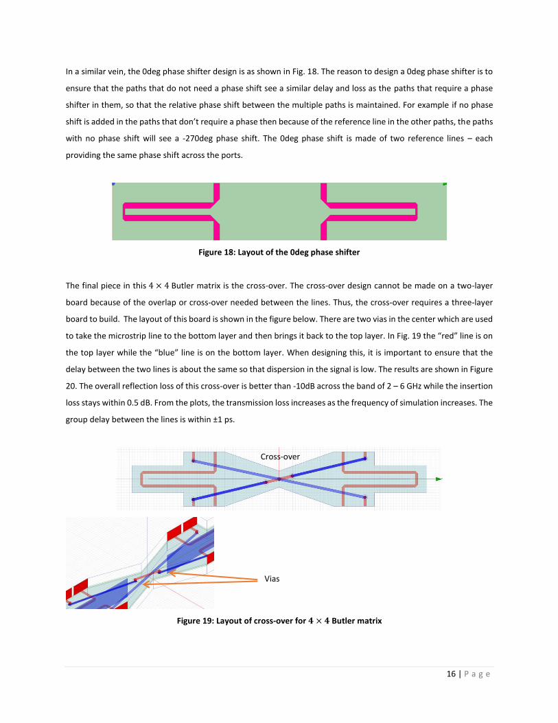
In a similar vein, the 0deg phase shifter design is as shown in Fig. 18. The reason to design a 0deg phase shifter is to
ensure that the paths that do not need a phase shift see a similar delay and loss as the paths that require a phase
shifter in them, so that the relative phase shift between the multiple paths is maintained. For example if no phase
shift is added in the paths that don’t require a phase then because of the reference line in the other paths, the paths
with no phase shift will see a -270deg phase shift. The 0deg phase shift is made of two reference lines – each
providing the same phase shift across the ports.
Figure 18: Layout of the 0deg phase shifter
The final piece in this 4 × 4 Butler matrix is the cross-over. The cross-over design cannot be made on a two-layer
board because of the overlap or cross-over needed between the lines. Thus, the cross-over requires a three-layer
board to build. The layout of this board is shown in the figure below. There are two vias in the center which are used
to take the microstrip line to the bottom layer and then brings it back to the top layer. In Fig. 19 the “red” line is on
the top layer while the “blue” line is on the bottom layer. When designing this, it is important to ensure that the
delay between the two lines is about the same so that dispersion in the signal is low. The results are shown in Figure
20. The overall reflection loss of this cross-over is better than -10dB across the band of 2 – 6 GHz while the insertion
loss stays within 0.5 dB. From the plots, the transmission loss increases as the frequency of simulation increases. The
group delay between the lines is within ±1 ps.
Figure 19: Layout of cross-over for 𝟒 × 𝟒 Butler matrix
Cross-over
Vias
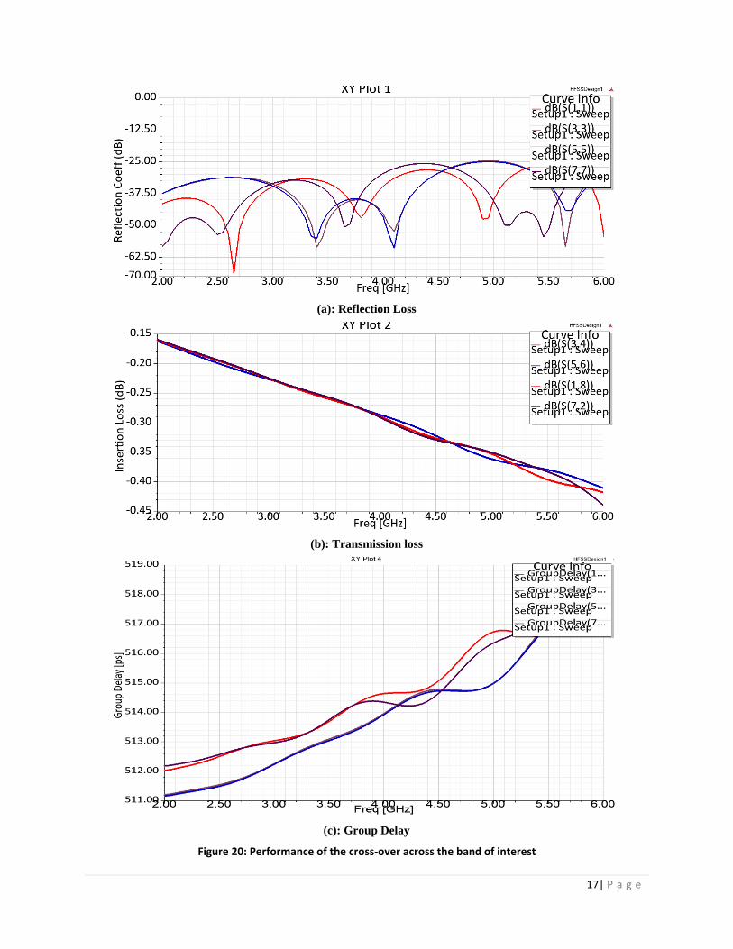
17| P a g e
(a): Reflection Loss
(b): Transmission loss
(c): Group Delay
Figure 20: Performance of the cross-over across the band of interest

18 | P a g e
With the completion of the cross-over design, the overall layout of the 4 × 4 Butler Matrix is shown in Fig. 21 below.
The measurements from this design will be presented in a future report.
Figure 21: Complete layout of 𝟒 × 𝟒 Butler matrix on a circuit card
3.2 The 𝟖 × 𝟖 Butler Matrix
The design of the 8 × 8 Butler matrix follows the same methodology as the 4 × 4 design. The additional components
that are needed is the 45deg phase shifter and a cross-over that interlaces 8 inputs and 8 outputs. This is a unique
design that was developed using just a three-layer board.
3.2.1 Design of 45deg phase shifter
To design the 45deg phase shifter, the length of the coupled line was increased from the line length that was used
for the 90deg phase shifter. By coupled lined length has to be increased such that the difference between the 270o
SMA Connectors
180o hybrid
Phase Shifter
Cross-Over
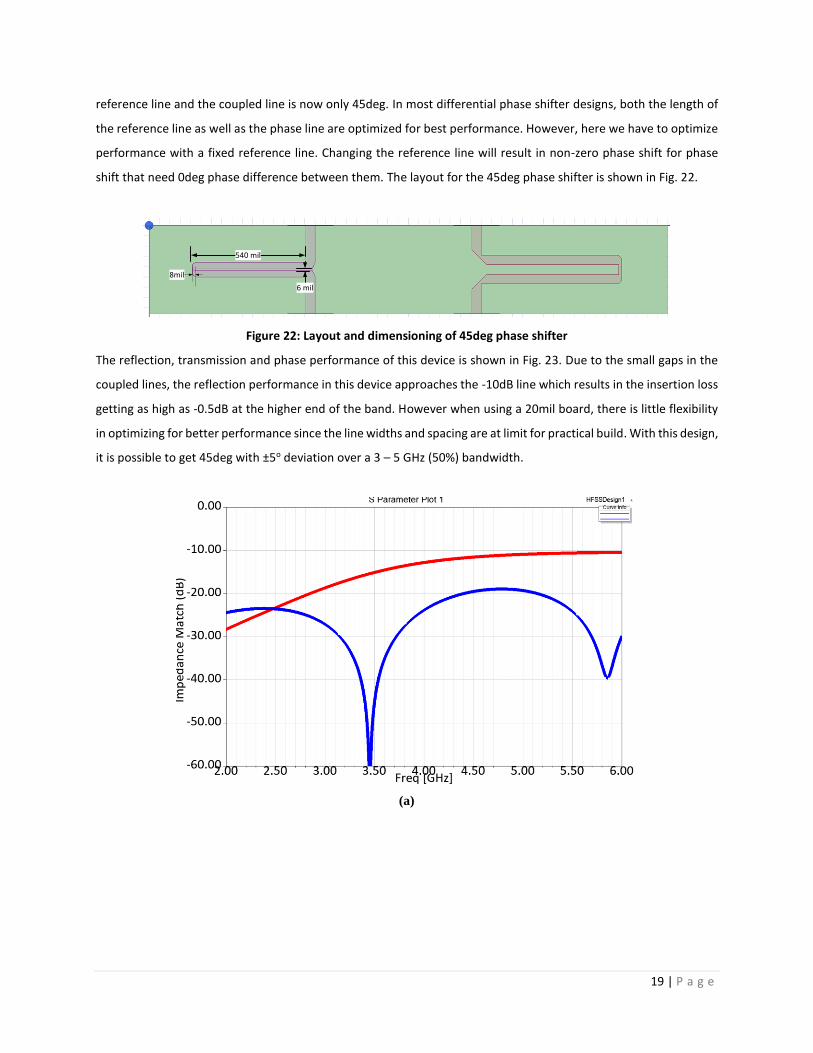
19 | P a g e
reference line and the coupled line is now only 45deg. In most differential phase shifter designs, both the length of
the reference line as well as the phase line are optimized for best performance. However, here we have to optimize
performance with a fixed reference line. Changing the reference line will result in non-zero phase shift for phase
shift that need 0deg phase difference between them. The layout for the 45deg phase shifter is shown in Fig. 22.
Figure 22: Layout and dimensioning of 45deg phase shifter
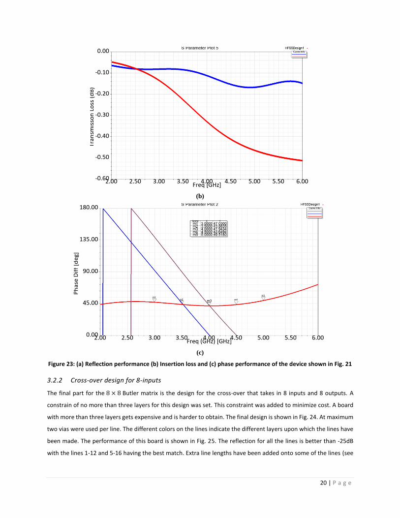
The reflection, transmission and phase performance of this device is shown in Fig. 23. Due to the small gaps in the
coupled lines, the reflection performance in this device approaches the -10dB line which results in the insertion loss
getting as high as -0.5dB at the higher end of the band. However when using a 20mil board, there is little flexibility
in optimizing for better performance since the line widths and spacing are at limit for practical build. With this design,
it is possible to get 45deg with ±5o deviation over a 3 – 5 GHz (50%) bandwidth.
(a)
540 mil
6 mil
8mil
20 | P a g e
(b)
(c)
Figure 23: (a) Reflection performance (b) Insertion loss and (c) phase performance of the device shown in Fig. 21
3.2.2 Cross-over design for 8-inputs
The final part for the 8 × 8 Butler matrix is the design for the cross-over that takes in 8 inputs and 8 outputs. A
constrain of no more than three layers for this design was set. This constraint was added to minimize cost. A board
with more than three layers gets expensive and is harder to obtain. The final design is shown in Fig. 24. At maximum
two vias were used per line. The different colors on the lines indicate the different layers upon which the lines have
been made. The performance of this board is shown in Fig. 25. The reflection for all the lines is better than -25dB
with the lines 1-12 and 5-16 having the best match. Extra line lengths have been added onto some of the lines (see
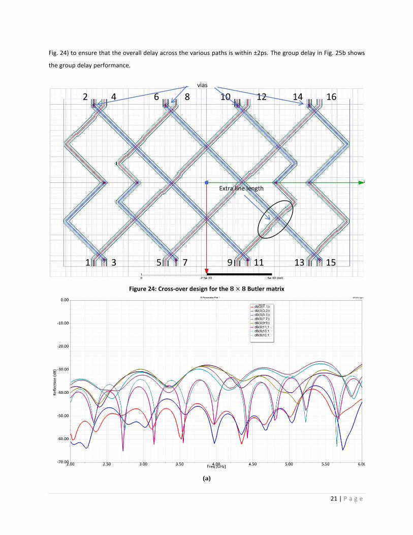
21 | P a g e
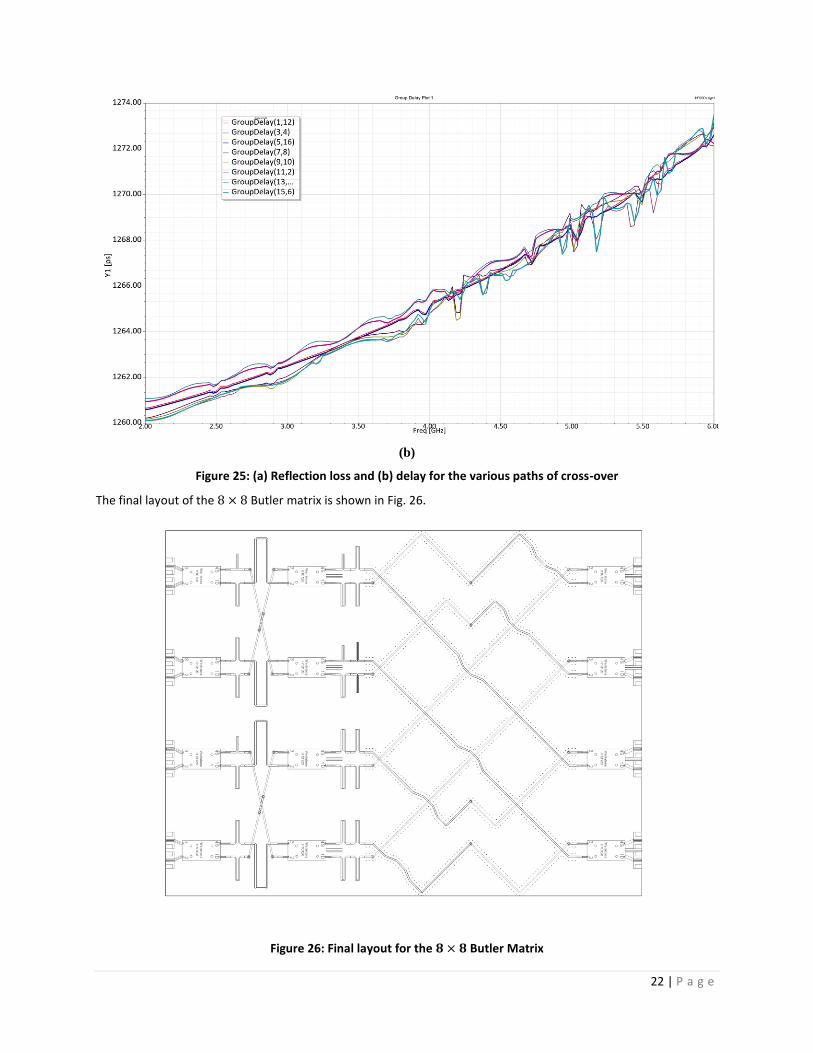
Fig. 24) to ensure that the overall delay across the various paths is within ±2ps. The group delay in Fig. 25b shows
the group delay performance.
Figure 24: Cross-over design for the 𝟖 × 𝟖 Butler matrix
(a)
2 4 6 8 10 12 14 16
1 3 5 7 9 11 13 15
vias
Extra line length
22 | P a g e
(b)
Figure 25: (a) Reflection loss and (b) delay for the various paths of cross-over
The final layout of the 8 × 8 Butler matrix is shown in Fig. 26.
Figure 26: Final layout for the 𝟖 × 𝟖 Butler Matrix

23 | P a g e
4. CONCLUSION
The objective of this report was to discuss in detail the steps taken to design the components needed to build Butler
matrices. These Butler matrices are necessary to build a passive network that can take as its input 𝑁 circular array
elements and output at most 𝑁 phase modes. These phase modes are all orthogonal to each other with unit
amplitudes and phases that cycle multiple times between 0 and 2𝜋. In an earlier report [1], we had discussed in
detail how the fixed-value phase shifters needed in the development of a Butler matrix can be calculated. Here in
this report, we describe in detail the steps taken to design and build these phase shifters. We have designed
differential phase shifters that can provide phases of 0deg, 45 deg and 90deg. These phase shifters have deviation
of about ±5 deg and can operate over a 50% bandwidth (3 – 5 GHz).
Additionally, we have also presented the designs of cross-overs needed to completely build 4 × 4 and 8 × 8 Butler
matrices. The steps presented in this report can be used to build phase shifters and cross-overs that can be used for
larger Butler matrices, with each larger Butler matrix getting more and more complex. For now, the plan is to build
the presented designs and measure them to compare the overall simulation vs. measurement performance. The
simulated and measured S-parameters will be used to feed a modeling and simulation tool which can be used to
design phase modes of any size circular array and analyze beamforming performance. The details of the modeling
and simulation tool will be presented in another report [13].

24 | P a g e
5. REFERENCES
[1] R. Mital, M. P. Parent and A. Stumme, "Circular Array Beamforming Using Phase Modes," Naval Research Lab,
Washington, DC, 2019.
[2] B. Shelag, "Butler submatrix feed systems for antenna arrays," IEEE Transactions on Antennas and Propagation,
vol. 21, no. 2, pp. 228-229, 2014.
[3] T. Macnamara, "Simplified design procedures for Butler matrices incorporating 90deg hybrids or 180deg
hybrids," IEEE Proceedings, vol. 134, no. 1, 1987.
[4] S. Z. Ibrahim and M. E. Bialkowski, "Wideband Butler Matrix in Microstrip Technology," in 2009 Asia Pacific
Microwave Conference, Singapore, 2009.
[5] M. E. Bialkowski, F. C. Tsai, S. Yu-Chuan and C. Kai-Hong, "Design of fully integrated 4x4 and 8x8 Butler matrices
in microstrip/slot technology for ultra wideband smart antennas," in Antennas and Propagation Society
International Symposium, 2008.
[6] L. Guo, H. Zhu and A. M. Abbosh, "Planar UWB Phase Shifter using parallel coupled lines combined with short-
ended stubs and impedance transformer," in 2015 Asia-Pacific Microwave Conference (APMC), Nanjing, 2015.
[7] L. Guo and A. Abbosh, "Multilayer phase shifter with wide range of phase and ultra-wideband performance,"
in 2013 Asia-Pacific Microwave Conference Proceedings (APMC), Nanjing, 2013 .
[8] S. El-Marini, J. Zibitou, R. Mandry, A. Errkik, A. Tajmouati and M. Latrach, "Design of 45 degree microstrip phase
shifter for beam forming network application using parallel coupled lines," in 2017 International Conference
on Wireless Technologies, Embedded and Intelligent Systems (WITS), 2017.
[9] A. M. Abbosh, "Broadband Fixed Phase Shifters," IEEE Microwave and Wireless Components Letters, vol. 21,
no. 1, pp. 22-24, 2011.
[10] J. P. Shelton, "Wideband TEM Components". Patent 3737810, 5 June 1973.
[11] L. Guo and A. Abbosh, "Ultra-wideband phase shifter using broadside-coupled microstrip coplanar waveguide,"
in 2013 Asia-Pacific Microwave Conference Proceedings (APMC), Seoul, 2013.
[12] J. L. Quirarte and J. P. Starksi, "Synthesis of Schiffman phase shifters," IEEE Transactions on Microwave Theory
and Techniques, vol. 39, no. 11, pp. 1885 - 1889, 1991.
[13] D. Scholnik, "Calibration and Optimization of a Wideband Circular Array Using a Phase Mode Beaformer," NRL
, in progress.


![[PPT]Tema 2.- MATRICES - Open Course Ware Moodle 2.5 · Web viewMATRICES PRODUCTO DE MATRICES POTENCIAS NATURALES DE MATRICES CUADRADAS MATRICES SUMA DE MATRICES. PRODUCTO DE UN ESCALAR](https://img.pdfslide.us/doc/110x75/5c17a16c09d3f2c7368c2ad2/ppttema-2-matrices-open-course-ware-moodle-25-web-viewmatrices-producto.jpg)