Embed Size (px)
Citation preview

Design and Development of a High
Frequency Mosfet Driver
Arthur James Swart
9557512
A dissertation submitted in fulfilment of the requirements for
the
Magister Technologiae: Engineering: Electrical
Department: Applied Electronics and Electronic Communication
Faculty of Engineering
Vaal University of Technology
Vanderbijlpark
Supervisor: Dr. H.C. vZ Pienaar
.
2005 -09- 3 0
FOR REFERENCE 0 l V

Declaration
I Arthur James Swart hereby declare that the following research information is solely my
own work. This thesis is submitted for the requirements for the Magister Technologiae:
Engineering: Electrical to the department of Applied Electronics and Electronic
Communication at the Vaal University of Technology, Vanderbijlpark. This dissertation
has never before been submitted for evaluation to any educational institute.
Arthur James Swart
08 November 2004
11

Acknowledgements
I want to hereby acknowledge Dr. Christo Pienaar for his contribution to the success of
this project. His continued encouragement and interest helped me surge ahead, continuing
to search for answers to the relevant questions at hand. His advice and experience proved
especially valuable when I was designing the Mosfet driver stage, and finally in
examining what the expected results should look like.
111

Dedication
This project is dedicated to my dearly loved wife, Charmain.
lV
Abstract
A high-power Mosfet was incorporated as a switching device into the efficient Class E
configuration, where the switching device switches current through itself either
completely on or completely off at high frequencies.
The first objective of this project was to demonstrate the effectiveness of a phase-lock
loop circuit in generating stable high frequencies when connected in an indirect
frequency synthesizer configuration. The indirect frequency synthesizer has established
itself as a versatile frequency generator capable of generating high frequencies based on a
lower stable reference frequency. The frequency generation stage incorporates a phase
lock loop circuit, a frequency divider and a stable reference frequency section. The
phase-lock loop section incorporates the TTL based 74HC 4046 that is based upon the
common CMOS 4046 integrated circuit. The frequency divider section is built around the
CMOS-based 4526 whilst the reference frequency section incorporates the CMOS-based
4060. The frequency synthesizer produced a range of frequencies from 50 kHz to 8 MHz
in 50 kHz steps. The output voltage was constant at 5,5 V.
The second objective was to show that the complementary emitter follower is indeed a
worthy Mosfet gate drive circuit at high frequencies. The Mosfet driver stage produced a
voltage signal of at least 11 V, being able to source and sink relatively high peaks of
current, especially at high frequencies. Voltage amplification occurred through the use of
multiple CMOS-based 40106 inverters. The complementary emitter follower, known for
its low output impedance and its ability to source and sink large amounts of current, was
an important component in the final Mosfet gate section.
v
TABLE OF CONTENTS
Declaration
Acknowledgements
Dedication
Abstract
List of figures
List of tables
List of annexures
Glossary of abbreviations and symbols
Chapter 1 Introduction
1.1 Background
1.2 Purpose
1.3 Methodology
1.4 Delimitations
1.5 Definition of terms
1.6 Importance of the research
1.7 Overview of the report
1.8 Summary
Chapter 2 The high-frequency generation stage
2.1
2.2
2.3
Introduction
Frequency synthesizer techniques
A theoretical overview of the indirect frequency synthesizer
Vl
ii
iii
iv
v
viii
X
X
xi
12
12
12
12
13
13
13
14
15
16
16
16
20

2.4
2.5
2.6
The indirect frequency synthesizer components
The design process of the high-frequency generation stage
Summary
Chapter 3 The Mosfet driver stage
3.1 Introduction
3.2 Theoretical overview of Mosfet switching techniques
3.3 The voltage amplification and gate drive sections
3.4 The design process of the Mosfet driver stage
3.5 Summary
Chapter 4 The results
4.1
4.2
4.3
4.4
Introduction
The results of the high-frequency generation stage
The results of the Mosfet driver stage
Summary
Chapter 5 Conclusions and recommendations
5.1
5.2
5.3
Introduction
Conclusions
Recommendations
References
List of Annexures
Vll
27
29
38
40
40 -
40
49
50
55
56
56
56
62
69
71
71
71
73
75
77

LIST OF FIGURES
Figure 1 Flow diagram of the design ofthe high-frequency Mosfet driver 14
Figure 2 An example of an incoherent frequency synthesizer 17
Figure 3 A coherent direct frequency synthesizer example 17
Figure 4 A coherent indirect frequency synthesizer 19
Figure 5 The block diagram of the common PLL circuit 20
Figure 6 The transfer function of a VCO 21
Figure 7 The phase detectors transfer function 22
Figure 8 The block diagram of the digital phase-lock loop otherwise known
as a frequency synthesizer 22
Figure 9 The bode diagram of a passive lag filter 23
Figure 10 The 74HC 4046 VCO's characteristic 25
Figure 11 Crystal oscillator configuration on the 4060 26
Figure 12 The 74HC 4046 functional diagram 27
Figure 13 The 4526 functional diagram 28
Figure 14 The functional diagram of the 4060 29
Figure 15 Cl and R1 from a predetermined VCO frequency 30
Figure 16 The low-pass filter network connected between pins 9,13 and ground 34
Figure 17 The improved low-pass filter incorporating the parallel capacitor
across R4 34
Figure 18 The complete circuit diagram of the TTL 74HC 4046 PLL 35
Figure 19 4526's connected in series to act as a maximum divide by 256 36
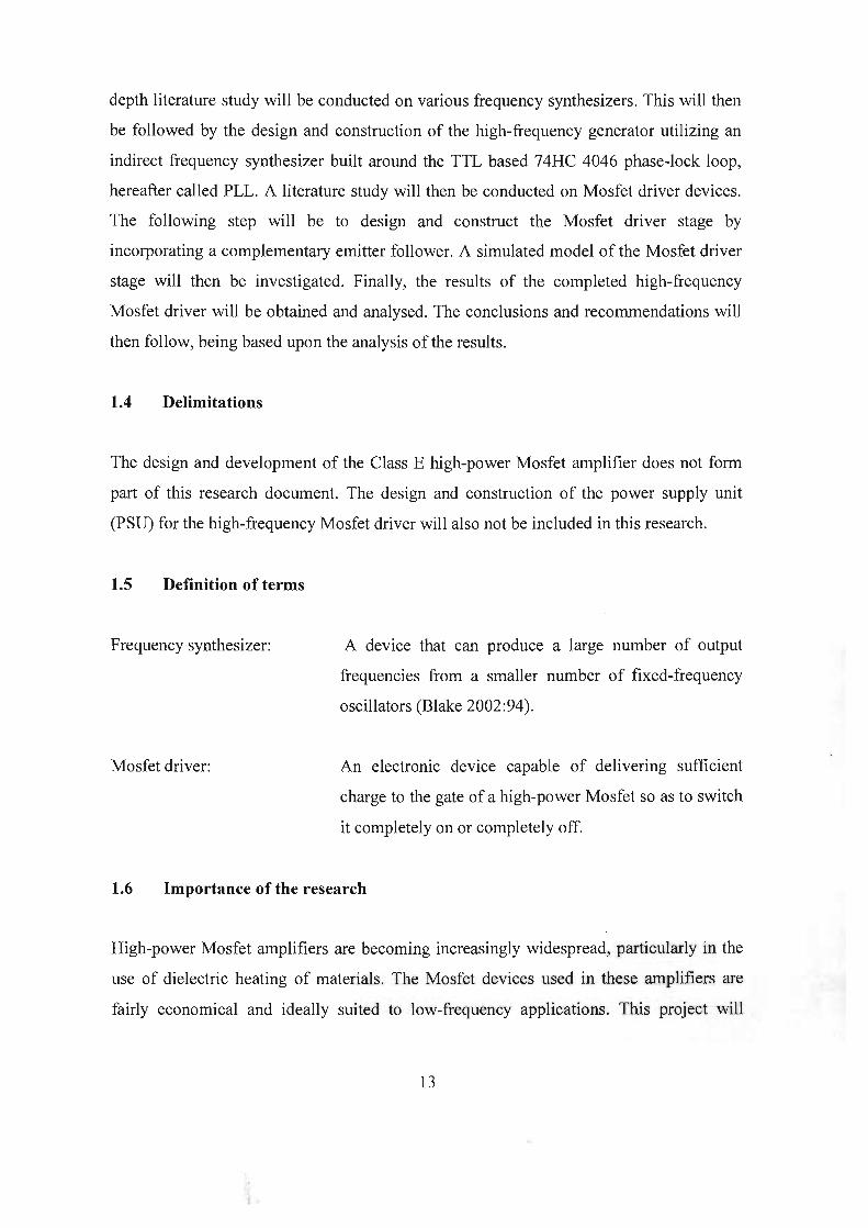
Figure 20 The reference frequency section built around the 4060 38
Figure 21 Driving the Mosfet/IGBT gates 41
Figure 22 Gate voltage to gate charge time with varying drain-source voltages 44
Figure 23 Asymmetric gate drives featuring a fast tum-on technique 45
Figure 24 Asymmetric gate drives featuring a slow tum-on technique 46
Figure 25 Gate drive circuits with inherent asymmetry 46
Figure 26 Complementary emitter follower, low impedance gate drive circuit 47
Figure 27 CMOS output paralled to increase drive capability 48
V111

Figure 28 A photovoltaic isolator used as a simple gate drive circuit 48
Figure 29 Logic diagram of a single inverter within the 40106 49
Figure 30 Switching input characteristics of the 40106 51
Figure 31 Four 40106's connected in series which provide the voltage
amplification of a square wave 52
Figure 32 The complementary emitter followers connected in series 53
Figure 33 The circuit diagram of the complementary emitter followers, as
present in the simulated package 54
Figure 34 The 7 MHz output frequency signal taken from test point A 56
Figure 35 The complete circuit/block diagram of the high-frequency Mosfet
driver 57
Figure 36 Frequency spectrum showing a 7 MHz frequency signal 58
Figure 37 Maximum possible output frequency of 8 MHz obtained at test
point A 58
Figure 38 Minimum possible output frequency of 50 kHz obtained at test
point A 59
Figure 39 Maximum output frequency of 8 MHz displayed by a spectrum
analyser 60
Figure 40 Minimum output frequency of 50 kHz displayed by a spectrum
analyser 60
Figure 41 Divider section's output frequency obtained from test point B 61
Figure 42 50 kHz output from the reference frequency section 61
Figure 43 The first 401 06's output within the voltage amplification section 62
Figure 44 The second 401 06's output within the voltage amplification section 63
Figure 45 The output of the third 40106 within the voltage amplification
section 63
Figure 46 The output of the fourth 40106 within the voltage amplification
section 64
Figure 47 Output frequency spectrum of the voltage amplification section 65
Figure 48 Output waveform of the first complementary emitter follower 65
Figure 49 Output waveform of the second complementary emitter follower 66
lX

Figure 50 The simulated models result of the high-power Mosfet where; A-
is the input to the Mosfet gate and; B - is the output from the
Mosfet drain
Figure 51 The input and output of the high-power Mosfet according to the
experimental model
Figure 52 The output of the complementary emitter follower when; X -
isolated from the Mosfet's gate and; Y- connected to the gate of
the high-power Mosfet
Figure 53 The simulated and experimental models result
Figure 54 Frequency spectrum portraying the output of the 2nd buffer stage
when connected to the gate of an IRF 61 0 high-power Mosfet
utilized in a Class E amplifier
LIST OF TABLES
Table 1 Comparison of incoherent, coherent direct and coherent indirect
frequency synthesizers
67
67
68
68
69
19
Table 2 Comparison of the three phase comparators used in the 74HC 4046 24
LIST OF ANNEXURES
ANNEXURE A 74HC 4046A Phase-lock loop with VCO datasheet 78
ANNEXUREB HEF 4526B programmable 4-bit binary down counter datasheet 112
ANNEXUREC IRF 140 HEXFET Power Mosfet datasheet 122
ANNEXURED HEF 40 1 06 HEX inverting Schmitt trigger datasheet 124
ANNEXUREE IRF 61 0 HEXFET Power Mosfet datasheet 131
ANNEXUREF Circuit diagram of the high-frequency Mosfet driver 137
ANNEXUREG Printed circuit board of the high-frequency Mosfet driver 138
ANNEXUREH The completed high-frequency Mosfet driver 139
X

GLOSSARY OF ABBREVIATIONS AND SYMBOLS
A
A- Amperes
AM - amplitude modulation
8
BVpp - Mosfet breakdown voltage in V
c C -Coulomb
COG- capacitance between the Mosfets drain
and gate in pF
CGs- capacitance between the Mosfets gate
and source in pF
C,.,_,. - the input gate capacitance of the Mosfet
in pF
CMOS - complementary metal oxide
semiconductor
D
d- Mosfet drift region thickness in 11m
DDS- Direct digital synthesis
E
Egare - energy expended in the Mosfet gate in J
EXOR - exclusive OR gate
F
f- the input gate frequency in Hz
I- the input Mosfet gate current in A
IC - integrated circuit
IGBT- insulated gate bipolar transistor
/ 0 - drain current set by the load impedance
J
J -Joule
J-K - a 5 input flip-flop device
K
Kr low-pass filter transfer gain
K. - inverse of the maximum or minimum
divider ratio
Kp- phase comparator gain
K, - VCO gain
kO- kilo Ohm being 103
kHz - kilo hertz being I 03
L
L - Mostet channel length in Jlffi
LF - low-pass filter
M
m- meter
MHz- Mega Hertz being 106
N
Ji- the lock range frequency in Hz N- the division factor
R
rad - radians
RG~nt! - the internal resistance oftl1e Mosfet
gate inn
R,. - the external resistance to the Mosfet gate
inn
s s- seconds
T
1 -settling time
11 -the positive time period of the frequency in
TIL - transistor-transistor logic
u 11H - micro Henry being I o-<·
v V - Voltage
vee- supply voltage v VCO -voltage controlled oscillator
V8_, - the gate to source voltage V
VT - Mosfet threshold voltage
w W- Watt
FM- Frequency modulation X, Y, z F00,- the VCO output frequency in Hz 0
Frer- the input reference frequency to the phase Symbols
comparator in Hz
FSK- frequency shift key
fr- transit time limited frequency response
G
GND- ground
gr, - Mosfet transconductance
H
Hz- Hertz
p
PD - phase detector
PFD - phase frequency detector
P"""- powered consumed in the Mosfet gate in
w pF - pi co farad being I o-'2
PLL - phase-lock loop
PSU -power supply unit
Q
Qgare - Mosfet gate control charge in C
Xl
n -Ohms
r, - the time constant set by R3 and C2 (to
give the roll off rate) ins
r 2 -the time constant set by R4 and C2 (to
give the roll off rate) ins
~- the damping ratio
11- micro being I o-<•
w,- natural frequency
Chapter 1 Introduction
1.1 Background
The generation of high frequencies has become part of mankind's history, especially
since the advent of the amplitude modulated radio at the beginning of the 20th century.
Initially, radio receivers primarily utilized amplitude modulation (AM) to modulate a
high carrier frequency with a lower audio frequency. In the latter part of the 201h century,
a demand arose for the generation of specific stable frequencies, at specific power levels,
thus meeting the needs of an ever-changing technological age. High-frequency generation
has now become a primary part of today' s radio communication field, featuring
prominently in many frequency modulation systems, otherwise referred to as FM
systems. Numerous other fields, such as the dielectric heating of materials, have also
come to include some or other form of frequency generation. These high-frequency
components must contain sufficient energy to be utilized effectively. The appearance of
the high-power Mosfet in the latter part of the 20th century made it possible to amplify
these high-frequency components to specific levels of usefulness.
1.2 Purpose
The purpose of this research project is to design and develop a high-frequency Mosfet
driver capable of driving high-power Mosfets, primarily within Class E configurations.
The high-frequency Mosfet driver must exhibit a high degree of frequency stability over
the range of 50 kHz to 8 MHz in 50 kHz steps. A selected frequency signa~ within this
range must then be able to successfully drive the gate of a high-power Mosfet that will
feed the load.
1.3 Methodology
The design and development of a high-frequency Mosfet driver for use in high-frequency
high-power Mosfet applications will be addressed in the following manner. Firstly, an in-
12
depth literature study will be conducted on various frequency synthesizers. This will then
be followed by the design and construction of the high-frequency generator utilizing an
indirect frequency synthesizer built around the TTL based 74HC 4046 phase-lock loop,
hereafter called PLL. A literature study will then be conducted on Mosfet driver devices.
The following step will be to design and construct the Mosfet driver stage by
incorporating a complementary emitter follower. A simulated model of the Mosfet driver
stage will then be investigated. Finally, the results of the completed high-frequency
Mosfet driver will be obtained and analysed. The conclusions and recommendations will
then follow, being based upon the analysis of the results.
1.4 Delimitations
The design and development of the Class E high-power Mosfet amplifier does not form
part of this research document. The design and construction of the power supply unit
(PSU) for the high-frequency Mosfet driver will also not be included in this research.
1.5 Definition of terms
Frequency synthesizer:
Mosfet driver:
A device that can produce a large number of output
frequencies from a smaller number of fixed-frequency
oscillators (Blake 2002:94).
An electronic device capable of delivering sufficient
charge to the gate of a high-power Mosfet so as to switch
it completely on or completely off.
1.6 Importance of the research
High-power Mosfet amplifiers are becoming increasingly widespread, particularly in the
use of dielectric heating of materials. The Mosfet devices used in these amplifiers are
fairly economical and ideally suited to low-frequency applications. This project will
13
address the current need for the successful switching of these high-power Mosfets at
higher frequencies, particularly within the Class E amplifier environment.
This research project will also address the need for a simplified, economically viable
frequency synthesizer to cover the high-frequency spectrum of 50 kHz to 8 MHz in 50
kHz steps. This type of frequency synthesizer can then be utilized as the source signal to
various communications equipment in a communications laboratory.
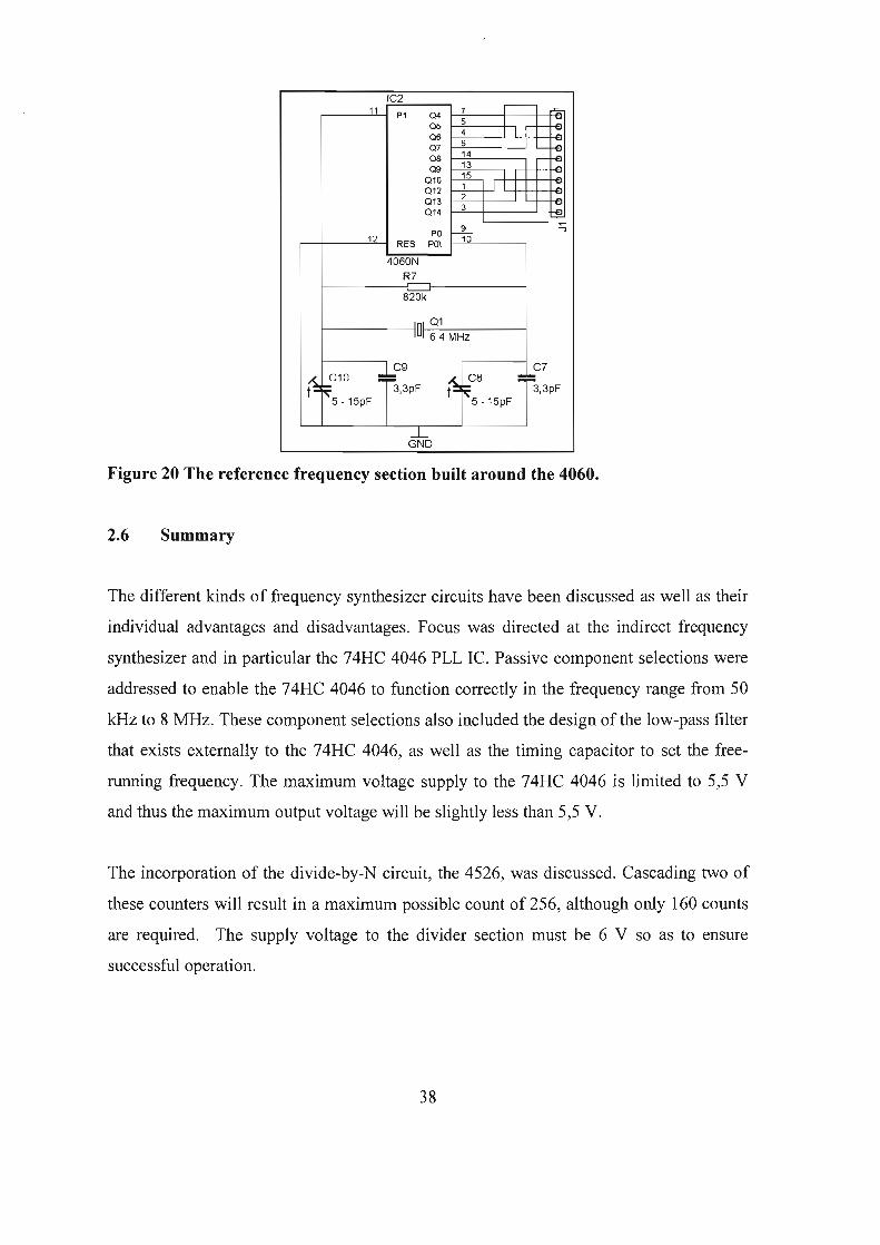
1. 7 Overview of the report
The project can be divided into two stages, namely the frequency generation stage and
the Mosfet driver stage. Figure 1 illustrates these two stages and their relevant sections by
means of a flow diagram.
High-frequency Mosfet driver
Chapter 2
High-frequency generation stage
PLL
section
Divider
section
Reference
frequency
section
Chapter 3
Mosfet driver stage
Voltage
amplification
section
Gate drive
section
Figure 1 Flow diagram of the design of the high-frequency Mosfet driver.
The design and development of the high-frequency Mosfet driver will start in chapter 2
with a discussion on coherent and incoherent frequency synthesizers. The choice of a
coherent indirect frequency synthesizer utilizing a PLL, programmable divider and stable
14

reference frequency will finally be considered as a possible high-frequency generator.
Problems associated with stability and frequency division will be analysed. The design
and development of this indirect frequency synthesizer will then be discussed as part of
the frequency generation stage.
Chapter 3 will contain an in-depth view of circuits and techniques currently employed to
successfully drive high-frequency high-power Mosfets. A voltage amplification section
utilizing, the HEX inverter 40 106 will be investigated to ensure a 12 V input signal to the
final gate drive section. The gate drive section incorporating a complementary emitter
follower will then be addressed. The final gate drive circuit will also be reviewed by
means of a simulation model.
The combination of the frequency generation and gate driver stages will be presented in
chapter 4. The results from the final completed high-frequency Mosfet driver will be
presented and analysed. The simulated model's result of the gate drive section will also
be analysed and discussed.
Chapter 5 will contain the conclusions and recommendations with regard to the high
frequency Mosfet driver.
1.8 Summary
The backgro•.md to the design and development of the high-frequency Mosfet driver has
been given. The methodology has been reviewed as well as the delimitations of the
project. Definitions of important terms were presented together with the importance of
the research and overview of the entire report. The following chapter will consider
frequency synthesis theory, circuitry and design.
15
Chapter 2 The high-frequency generation stage
2.1 Introduction
According to Blake (2002:6), the low-frequency band extends from 30kHz to 300kHz,
the medium-frequency band from 300kHz to 3 MHz and the high-frequency band from 3
MHz to 30 MHz. The high-frequency generation stage must produce a range of frequency
from 50 kHz to 8 MHz, and thus incorporates all three of these bands. Chapter 2_wi1l
focus on various frequency synthesis techniques that have been employed to generate
high frequencies'. Various kinds of frequency synthesizers will be presented with
attention primarily directed to the indirect frequency synthesizer and its components. The
design process of the indirect frequency synthesizer incorporating the TTL based 74HC
4046 PLL, the CMOS based 4526 programmable divider and the CMOS based 4060 14-
stage counter will then follow.
2.2 Frequency synthesizer techniques
A frequency synthesizer is a combination of system elements that results in the
generation of one or many frequencies from one or a few reference sources. The
frequency -accuracy and stability of these devices are determined primarily by the
accuracy and stability of the crystal and to a lesser extent by the circuit itself. The single
crystal-controlled oscillator circuit was superseded by an approach currently referred to
as incoherent synthesis. This method utilized a number of crystal-controlled oscillators
combined in such a fashion as to generate many frequencies with relatively few crystals.
The reference frequency is directly translated using analog techniques such as switching,
frequency division, frequency multiplication, filtering and mixing. This approach was
eventually improved by the use of just one reference source to produce numerous
frequencies and came to be known as coherent synthesis (Manassewitsch 1987:1 ). Figure
2 represents a typical incoherent frequency synthesizer while figure 3 shows an example
of a coherent direct frequency synthesizer.
16

5.009 MHz
Crystal oscillator
[ 3 : 5.0 MHz
11.029 MHz
Mixer +
....-8-an-d---pa-ss---,J l r--M-ix-ar---, I
~ filtEr ~ + ~' 1 11.0-11.1 MH I I
16.02 MHz
Crystal oscillator
{2 = 6.0 MHz
47.1 MHz
Crystal
I oscillator
[ 1 " 47.0 MHz
r--- j ____ -----------'- -------------- -- -,_ I L I ~~~ I • • ' I a·:;; I •• ··r ·1:~~ ~ -1 I-1-c:------- ---lJ- - _________ J._ -1- JLt ~
Cl Cl = 0 0 DO CJ Cl DO = TIJ1T TII!T TTJ1 T
N .... .... N N N N N N N N
~ :r :r :r :r :r :r :r :r :r :r :r ::;; ::;; ::;; ::;; ::;; ::;; ::;; ::;; ::;; ::;; ::;; ::;;
§ ~ N § 8 0 N
~ q N Cl! 8 0 ,.; ~ u:i u:i u:i ... ...
lri In lri It) <D ... ... ...
Band -pass filter
58-59 MHz
58.129 MHz
Figure 2 An example of an incoherent frequency synthesizer (Manassewitsch
1987:5).
1 MHz referon~
] Multiplier ~R Multiplier ~MM Multiplier l 20.0 MHz
j_ l X2 X2 X5 I I
I Divider Multiplier t 1.5 MHz ] Mixer I 21.5 MHZ .. 2
1 X 3 ]I I + I
I 0.5 MHz
J Mixer I I 2.0 MHz 22.0 MHz
I + I 1.5 MHz
_l Mixer I 23.5 MHz
I + I 4.0 MHz j Mixer I 24.0 MHz
I + j t 1.5 MHz _t Mixer I 25.5 MHz
I + I
Figure 3 A coherent direct frequency synthesizer example (Manassewitsch 1987:8).
17

Frequency synthesis may thus be classified into two distinctive groups, namely coherent
frequency synthesis and incoherent frequency synthesis. The coherent frequency
synthesizers can furthermore be classified into coherent direct frequency synthesizers and
coherent indirect frequency synthesizers.
Browne (2003: 1) notes that the demand for synthesized sources with a wide range of
performance levels is growing, as tuning in high-frequency systems is now dominated by
digital approaches - tuning frequencies in discrete steps - rather than earlier analog
methods, which utilized continuous tuning. Various techniques are currently utilized in
modern frequency synthesizers, such as the "integer-N" synthesizer, the "fractional-N"
synthesizer and the direct-digital synthesizer. These latter ones rely on the principle of
conversion of 32-to-48-bit phase/frequency/amplitude digital data into analog output
signals through use of precision accumulators and digital to analog converters. Direct
digital synthesis (DDS) is an example of a coherent direct frequency synthesizer, where
the output signal is created as a one-to-one function of an input digital word. This allows
high-speed frequency switching and execution of such functions as frequency hopping
and generation of complex chirp signals. Direct frequency synthesis may also be
achieved via analog circuitry, where a comb of frequencies are generated and then
filtered out to produce the required frequency components. The amount of filtering
needed for high-frequency and broadband coverage leads to a design that is complex and
expensive. The "integer-N" synthesizers use a multiplication factor, N, to determine the
output frequency as a multiple of the reference source frequency. The "fractional-N"
synthesizer is similar to an "integer-N" synthesizer but makes use of non-integer values
for N. The "integer-N" synthesizer may be designed with a single loop for optimal
frequency switching speed, or with multiple loops when lower noise performance is
required. The "integer-N" synthesizer can achieve phase-noise levels that are close to the
reference source, although they tend to be limited in bandwidth. This "integer-N"
synthesizer forms part of the coherent indirect frequency synthesis group (Browne
2003: 1). An example of an indirect frequency synthesizer is shown in figure 4. Table 1
contains a summary of the advantages and disadvantages of incoherent and coherent
frequency synthesizers.
18

-I
Phase Detector
Loop Filter
Programmable Djvider
vco
Figure 4 A coherent indirect frequency synthesizer (Blake 2002:86).
Table 1. Comparison of incoherent, coherent direct and coherent indirect frequency
synthesizers.
Advantage Disadvantage
Incoherent frequency Very high output purity Very high complexity
synthesizer Many components
Many crystals
Coherent direct Low spurious tone levels Very high complexity
frequency synthesizer Low phase jitter Many components
One Crystal
Coherent indirect Very easy to implement
frequency synthesizer Easily integrated
Few components
One crystal
The above table indicates that coherent indirect frequency synthesizers are much easier to
design and implement. Having fewer components than their counterparts leads to a
reduction in both cost and size. Finally, the wide availability of both PLL and divider
circuits makes them the ideal choice for use in high-frequency generation, and wiU thus
be utilized in this research project.
19

2.3 A theoretical overview of the indirect frequency synthesizer
Lythall (2002: 1) presents the indirect frequency synthesizer as an arrangement whereby
the reference frequency is multiplied by a programmable amount to achieve just about
any frequency within a selected output frequency range. Best (1984:vii) describes the
PLL circuit as an exotic device, found within specific electronic devices present in
practically every home worldwide today. Indeed, the PLL is one of the most versatile
sought after designs when it comes to stable frequency generation (Best 1997:1 ). Van
Roon (200 1 : 1) mentions a French scientist, H. de Bellescize, who in 193 2 already
published findings on PLL's called "La Reception Synchrone", published in Onde
Electrique, volume 11. Van Roon (200 1:1) further relates that the initial cost of the PLL
circuit outweighed its counterparts and thus prohibited the widespread use of this
technology. The PLL circuit did though become very popular when monolithic integrated
circuits were developed, with complete PLL circuits being housed in these low-cost IC
packages. From the 1940's on, the applications of the PLL circuit included
synchronization of the horizontal and vertical sweep oscillators in television receivers to
the transmitted sync pulses. AM and FM demodulators, frequency shift key (FSK)
decoders, motor speed controls, touch-tone decoders, light-coupled analog isolators and
frequency synthesized transmitters and receivers all make use of PLL circuitry today.
F ref Phase Low-pass Voltage F out
detector filter controlled oscillator
Figure 5 The block diagram of the common PLL circuit.
Best (1997:2) defines the PLL as a circuit synchronizing an output signal, generated by
an oscillator, with a reference or input signal in frequency as well as in phase. Once
synchronized or locked, the phase error state between the output and input frequency is
virtually zero. He sketches the block diagram of the PLL circuit as containing three
20

distinct and separate sections, namely the phase detector (PD), low-pass filter (LF) and
voltage controlled oscillator, hereafter called VCO. Berlin (1982:5-17) furthermore
describes the PLL as a circuit incorporating an electronic feedback loop system
consisting of a phase detector, low-pass filter and VCO. The block diagram of the PLL is
sketched in figure 5.
Brennan (1996:26) describes the VCO as an electronically tuneable oscillator in which
the output frequency is dependent on the value of an applied tuning voltage. VCO's are
realised in many forms from RC multivibrators at low frequencies to varactor oscillators
at higher frequencies. The most important property of a VCO is their tuning characteristic
that is also referred to as the VCO's transfer function. This non-linear transfer function of
input voltage to output frequency is shown in figure 6.
VCO gain 350MHz
10 MH1JV
'N' JOOMHz ::r: ,.-..,
~ 7.5 MH71V ~ '-" >-. ::r: (.) 250 !YJHL. ~ t:: Q) '-" ;::l
t:: cr' 5MHz/V ·.-< Q) (\j <.l:1 bO
0 200MHz 0 u VCO frequency u > >
5 10 15 20
Tuning voltage (V)
Figure 6 The transfer function of a VCO (Brennan 1996:27).
Best (1997:2) illustrates the transfer function of the phase detector as a function of the
average value of the phase detector output signal to the phase error. This difference in
phase value then generates a phase error as a DC voltage that is passed by the low-pass
filter to the VCO. This DC voltage then serves to move the output frequency of the VCO
either up or down, depending on its initial point of rest. The transfer function of the phase
21

detector is sketched in figure 7, where the optimum points of operation are between +n
and -n.
', ~e ( deg)
'
Figure 7 The phase detectors transfer function (Best 1997:95).
u 1,W1
Digital Ud Analog Ut vco U2 I
... ______.. PO LF
W2
I
+ N Counter t I
u2 ,w2 (optional)
Figure 8 The block diagram of the digital phase-lock loop otherwise known as a
frequency synthesizer (Best 1997:91).
From the 1970's on, the digital phase-lock loop, or DPLL, made its appearance. The
DPLL included a divide-by-N counter in its configuration. The phase detector was
constructed from EXOR gates or JK flip-flops, although the rest of the components were
still analog. An improved phase detector later emerged that made use of 2 D-Type flip
flops connected to a NAND gate and comparator. This type of detector makes use of
22

positive edge triggering, being influenced only by the initial positive going edge of the
incoming pulse signal. Best calls this improved phase detector a "Phase Frequency
Detector", or PFD. He also accredits the PFD as the main workhouse of the DPLL circuit,
incorporating no passive components. The classical DPLL block diagram is shown in
figure 8, which is also termed the frequency synthesizer circuit (Best 1997 :92). Voltage
u1 at frequency w1 is the reference frequency obtained from a stable reference source,
such as a single quartz crystal. The VCO's output frequency is represented by u2, w2
while u2',w1' is the divided frequency obtained from the divide-by-N counter. The PLL
circuit comprising the VCO and phase detector have become widely available in
integrated circuit packages such as the CMOS-based 4046. The divide-by-N counter is
also housed in a separate integrated package, or IC, external from the PLL section. The
low-pass filter is the only section that features externally with passive components. The
simplest loop filter configuration, being that of passive lag, is easily implemented with
the 4046 (Best 1997: 152). Figure 9 illustrates the bode diagram of a passive lag filter.
IFI
1~r-----...... -20 dB/decade
~--------~--------+-------~--~w
Figure 9 The bode diagram of a passive lag filter (Best 1997:9).
Best (1997:152) did a case study on frequency synthesizers, in which he considered the
74HC 4046. He noted the usefulness of the 74HC 4046 in generating high frequencies.
This is verified in the datasheet specifications of the 74HC 4046 (Annexure A). The
74HC 4046 PLL circuit contains three different phase detectors, namely an EXOR gate, a
PFD and a JK flip-flop. Table 2 provides a summary of the individual advantages and
23

disadvantages of the three phase detectors/comparators that are utilized in the 74HC
4046.
Table 2. Comparison of the three phase comparators used in the 74HC 4046.
Phase Phase Phase
comparator 1 comparator 2 comparator 3
EXOR flip flop D-type flip flop JK flip flop I I
Capture range dependant on Yes No Yes
the low-pass filter
Noise rejection at signal High Low Low
input
PLL locks onto harmonics of Yes No Yes
the VCO centre frequency
Phase difference between 90° oo 180°
input and output locked
signals
Input signals duty cycle Must be 50% Not important Not important
Best (1997:152) also plotted the VCO's characteristic as illustrated in figure 10. The
linear operational range of the VCO was found to be between 1,1 and 3,9 V, when the
output frequency changed from 1 to 2 MHz. The results obtained from the case study
done by Best as well as the datasheet specifications highlights the following advantages
of74HC 4046:
• High-frequency generation up to 20 MHz.
• Constant 5 V peak output signal over the 20 MHz range.
• A choice of three different comparators or detectors.
• Linear input to output range of the VCO.
The 74HC 4046 will be used in this research project due to the advantages mentioned
above. Phase comparator 2 will be chosen due to its advantages highlighted in table 2.
24

N ~ 2 ::L
~
I 1 -
0
GOLDFIELDS LIBRARY
1.1
r---1 I I
3.9 5 _ _.,. Uf {V)
Figure 10 The 74HC 4046 VCO's characteristic (Best 1997:153).
The division of frequencies plays an important role in the function of any frequency
synthesizer circuit. When a counter is used between the output of the VCO and the one
input to the phase detector, the VCO then generates a frequency that is N times the
reference frequency resulting in (Best 1997:92),
.... (2.1)
WhereFout =the VCO output frequency in Hz
F ref = the input reference frequency to the phase comparator in Hz
N =the division factor
Berlin (1982:5-17) states that the divide-by-N counter is a logic circuit that produces a
single output pulse for every N input pulses, where N is an integer. Often referred to as
the modulus of the counter, the value ofN can easily be changed to a different value and
thus also affect the output value of the VCO. The CMOS-based 4526 is one of the best
known programmable cascaded down counters according to Marston (1996: 196). A
single counter has a maximum count of 16. The greatest advantage of the 4526 is the ease
at which multiple counters may be cascaded together to obtain higher N counts. The
reference frequency may then be made smaller resulting in the output frequency being
adjustable in smaller frequency steps. The 4526 has the following advantages:
25

• High-frequency operation up to I 0 MHz when fed with a 6 V power supply.
• Numerous counters may be cascaded together for higher divide-by-N counts.
The 4526 will be incorporated into this research project to function as the divide-by-N
counter.
Lastly, a reference frequency must be obtained from a stable source. Berlin (I982:5-I3)
notes that the PLL synthesizer can only work correctly if based on a stable reference
frequency. The frequency must be held constant over a period of time and under varying
temperature conditions, otherwise the output VCO frequency will drift according to the
input reference frequency, which is unacceptable. This is avoided by using a very stable
oscillator, such as a quartz crystal oscillator that has the advantages of greater accuracy
and stability (Blake 2003 :72).
I2
Crystal
I5pF 5-25pF
Figure 11 Crystal oscillator configuration on the 4060.
Marston (1996:267) explains that a crystal oscillator can be used to provide precision
submultiples of the crystal frequency by feeding the crystal's output through a suitable
number of digital divider stages, or a divide-by-Q counter. The CMOS-based 4060 is a
I4-stage ripple carry binary counter, which can directly accept any crystal value up to I 0
MHz. Figure II illustrates the capability of the 4060 to accept a quartz crystal in a Pierce
oscillator configuration. Multiple cascaded stages within the 4060 offers the possibility of
26

dividing the crystal frequency by a factor of 2n, where n represents the number of selected
stages. The following two advantages of the 4060 can be noted:
• It directly accepts crystals up to a value of 10 MHz.
• It can divide the original input frequency by a factor of 2n, and can thus function
as a divide-by-Q counter.
The 4060 together with a quartz crystal will thus be included in this research project to
function as the reference frequency section.
2.4 The indirect frequency synthesizer components
Today's technology has evolved at such a rate that many PLL circuits are available on the
market in IC package form. One package of special interest is the TTL package, the
74HC 4046. The 74HC 4046 PLL functional diagram is shown in figure 12.
-H-6 7 4 3
C1A c1 8 Vco OUT COMP1N
12 R2
R2~ vco
~ 11 R1
R1 [l :'.7. -V
'--
INH DEMouT VCOIN
5 10 9
~ Rs
7,
14
SIGIN
4046A
>-- PHASE PC1ouT 2 COMPARATOR
1
PC2ouT 13 >-- PHASE
COMPARATOR PCPouT 1 2
- PHASE PC3ouT 15 COMPARATOR
3
I I I I \ \
-.. \ R3 ',~---r-1-~~ I
~ I
I I
I I
I I R4~
C2 ......
+
Figure 12 The 74HC 4046 functional diagram (Philips Semiconductors 2004).
The 74HC 4046 will be utilized as the PLL circuit in the frequency synthesizer to obtain
the frequency range of 50 kHz to 8 MHz. The advantages of using the 74HC 4046 have
27

been presented in the theoretical overview. The 3 different phase comparators and VCO
are housed inside the IC as shown in figure 12. The low-pass filter is the only external
part, connected between the phase comparator's output and the VCO's input.
The divider circuit will be based upon the 4526, a programmable 4-bit down counter.
Multiple connections of this device in series create higher division orders, with the
highest input frequency being 10 MHz at a supply voltage of 6 V, according to the
datasheet. The division factor can be set by means of 4-pole dipswitches. See annexure B.
The functional diagram of the 4 526 is shown in figure 13.
3 5 11 14 2 I
PL Po p1 p2 p3
PARALLEL LOAD ~ CIRCUITRY
6 CPo CofSo BINARY
- CP DOWN 4 cP1 COUNTER
Co
03 1 02 15
10 MR 01 9 oo 7
~
ZERO TC 12
13 CF DETECTOR
7Z841 09.1
Figure 13 The 4526 functional diagram (Philips Semiconductors 2004).
The reference frequency that will be utilized in controlling the output frequency of the
VCO must be very stable, so as to prevent the output VCO's frequency from drifting
uncontrollably. A 4060 will be utilized in conjunction with a quartz crystal so as to obtain
28

a variety of reference frequencies. The functional diagram of the 4060 is illustrated in
figure 14, where Q4 through Q14 represent the respective output divided frequencies.
I'
RESET 14-BIT RIPPLE COUNTER ClK
Q12 013 01<4 04 Vss (GND)
Figure 14 The functional diagram of the 4060 (Marston 1996:161).
2.5 The design process of the high-frequency generation stage
The first step is to implement the design criteria for the 74HC 4046 to achieve a free
running frequency with a desired lock range from 50 kHz to 8 MHz. Secondly, the
inclusion of the 4526 as the frequency divider will be reviewed, as the output frequency
must be changed in steps of 50 kHz. Finally, the generation of the 50 kHz reference
frequency via the 4060 and quartz crystal will be considered.
The 74HC 4046's free-rurming frequency together with its capture and lock range are set
via an external capacitor, C1, connected between pins 6 and 7, and by a resistor R1
connected between pin 11 and ground. Figure 18 shows the position of C 1 and Rl. For a
free-rurming frequency of 2 MHz and a maximum lock frequency of 8 MHz, values for
C 1 and R 1 can be selected by utilizing figure 15. The values for R 1 would be 3 kQ and
for C1 around 300 pF. It was found that R1 's value is correct around 3,3 kQ, but C1 was
not confirmed. Instead, a value of 33 pF was utilized that achieved the desired results.
29

101 ,,, '
Ia (Hz}
AI• lkl I
107 , - t( lkO_{
~
""' ~ ~ 101
I• 1aa <n
:~w 1•30! k[ ~
~ ~
~ ~ ""' ~ ~ 1a•
~
&. ~
~ ~ " f:§~ ~ 1a4
&. ~ 'vee~
1a3 ~ ~ "~~ •. 5v
ev
~ 3v !az ~ ~
I
~ ~3·
10 ::·~ 1 Ia 102 IOl 104 1a1
Cl (pFI Ia 107
Figure 15 Cl and Rl from a predetermined VCO frequency (Philips
Semiconductors 2004).
The inclusion of R2 creates a DC offset for the free-running frequency. This DC offset is
handy when working at lower frequencies below 4 MHz, especially when utilizing the
standard 4046 PLL. The introduction of R2 in the 4046 enables a higher stability and a
decrease in the overshoot and ringing of the final VCO output frequency. Its application
is though not warranted in the 74HC 4046, as it was found that it introduces instability
and an oscillation at frequencies above 4 MHz. It will thus be ignored in this design and
be considered as an infinitely high resistance to ground. The low-pass filter's values can
be determined for a desired lock range of 7,950 MHz, a settling time of 1 ms and a supply
voltage of 5,5 V at the maximum frequency point. The following equations for the
calculation of the low-pass filter are taken from the datasheet in annexure A.
30
I

The veo gain (Kv) is given by,
K = 2xfLx2xJr v 0,9-(Vee-0,9)
Where fi =the lock range frequency in Hz
vee =the supply voltage v
Thus calculating the veo gain of the 74He 4046 results in,
2x7950xl03 x2xJr Kv =
0,9- (5,5- 0,9)
Phase comparator gain (Kp) is calculated by,
K =vee P 4x 7r
K =_22__ P 4x 7r
The transfer gain of the low-pass filter (K1) is determined by,
K _ 1 +r2
/-1+(-rl +r2)
... . (2.2)
.... (2.3)
.... (2.4)
Where r 1 =the time constant set by R3 and e2 (to give the roll off rate) ins
r 2 =the time constant set by R4 and e2 (to give the roll off rate) ins
Refer to figure 18 for the position ofR3, R4 and e2.
31

The natural frequency (U>n) is defined by,
({) = n
Kp X Kv X Kn ----'----- s·I
(ri + r2) .. .. (2.5)
Where Kn is the inverse of the maximum or minimum divider ratio being,
N . = Fout(rnin)
rnon F ref
N . =50 kHz rnon 50 kHz
Nrnin = 1
N = Foul(max)
max F ref
N = 8 MHz max 50 kHz
Nmax = 160
.... (2.6)
-· .. (2.7)
A damping ratio ( c;) of 1 will cause an overshoot of less than 15% and will settle to
within 2% at eont = 5, according to the datasheet. See annexure A. The settling time (t)
has already been given as 1 ms. Thus, eon is calculated as,
5 ({) =
n f
Now rewriting equation 2.5 results in,
K xK xK ( rl + r 2) = p ; n
(ljn
.... (2.8)
.... (2.9)
The maximum overshoot will occur at the maximum natural frequency of equation 2.8,
thus,
32

( ) 0,437x26,8xl06
'[ + '[ = ---'---------::---'---1
2 50002 xl60
(r, +r2 )=2,928 ms
Thus if C2 equals 100 nF then R4 equals,
R 4 = ( r, + '[ 2) X 2 X UJn X~ -1
KPxKvxKnxC2
Where ~ = the damping ratio
R4
= [2, 928x 10-3 x 2x 5000x 1-l]x 160
0, 437 x 26,8 x 106 x 1 OOx 10-9
R4=3,8 kQ
R3 is then calculated as follows,
R3 = _5___ R4 C2
R3 = 2,528xlo-3 -3800 1 oo x 1 o-9
R3 = 21,5 kO
R3=22 kO
.... (2.1 0)
.... (2.11)
The low-pass filter, including component values, is sketched in figure 16. R3 is
connected between the VCO's input and phase comparator 2's output. Lythall (2002: 1 ),
in his improved frequency synthesizer design, includes a 4 70 nF capacitor in parallel with
R4. This serves to decrease the wide "skirt" found at the bottom of the fundamental
frequency, thus improving the overall spectral purity. It also significantly improves the
lock range and increases the stability of the output VCO frequency. The output frequency
of the VCO tends to oscillate uncontrollably on the outskirts of the lock range. The
improved low-pass filter design, depicted in figure 17, inhibits this uncontrolled
33

oscillation to a degree, thus ensuring an excellent lock range from 50 kHz to 8 MHz. The
phase noise of the system is also significantly reduced.
IC1
GIN pp VCOOUT PC1
SIGIN PC2 13
ex ("')
0:::
ex VCOIN 9
INH N c ()
R1 DEMO 0
R2 ZEN 0 ......
744046N -.;t co ..lo::
0::: ("')
GI\JD
Figure 16 The low-pass filter network connected between pins 9,13 and ground.
IC1
eiN pp 2 VeOOUT Pe1
SIGIN Pe2 13
ex (')
0::
ex VeOIN 9
INH 10 R1 DEMO 15 e3 R2 ZEN
744046N co 470nF ~ (')
GND
Figure 17 The improved low-pass filter incorporating the parallel capacitor across
R4.
The PLL circuit incorporating all component values is illustrated in figure 18. The timing
capacitor, Cl, together with Rl are responsible for setting the free-running frequency of
the PLL and has been chosen to be 33 pF. Capacitors C4 and C5 serve to DC de-couple
34

the VCO's input from the divider's output and the VCO's output from the divide-by-N
input respectively. The input reference frequency to pin 14 on the PLL is also DC de
coupled via C6. R5 and R6 form a resistive network to ensure correct impedance
matching between the reference frequency section and the PLL. The supply voltage is set
to 5,5 V.
To Divider From Divider
...l..C5 ...l..C4
330nF 330nF
IC1 3 eiN pp 1
From Reference 4 2 VeOOUT Pe1 R6
14 13 SIGIN Pe2 5 LL.. (!)
c () 6 0 ex
("") ("") ("") 0:::
F 7 ex VeOIN 9 ~
lO 0 INH
10 ("") R1 DEMO 0::: ("")
15 C3 R2 ZEN
.,.... 0:::
470nF
GND
Figure 18 The complete circuit diagram of the TTL 74HC 4046 PLL.
The operating frequency range ofthe VCO is set between 50 kHz and 8 MHz. This must
be adjustable in 50 kHz steps, which thus necessitates the use of a divider circuit. The
minimum required division factor is 1, as calculated earlier in equation 2.6. The
maximum value was found to be 160 from equation 2.7. To achieve a maximum division
factor of 160 will require two counters to be cascaded, as one 4526 can only provide a
maximum count of 24 = 16. Using two 4526's results in a maximum division factor of
28 = 256. The configuration of the two counters, the 4526's, is portrayed in figure 19.
Connecting multiple 4526's together is made possible by means of CF (Carried forward
function). Pins DPO to DP3 serve as the input pins to set the division value to a
predetermined amount. These pins should never be left floating, as this wiU cause the
4526 to operate incorrectly. They must either be connected to ground via a 1,8 kO
35

resistor to represent a "zero", or they must be connected to vee to represent a "one".
The master reset, MR or RES pin, needs to be grounded for the divider circuit to function
correctly. All parallel load inputs, PL or PE inputs, must be connected together to ensure
that the 4526 divider circuit operates in a cascade configuration. The clock input of
successive counters is also connected to the maximum output pin of the forgoing counter.
From the datasheet of the 4526 it is noted that the output frequencies from these circuits
do not have a duty cycle of 50%, but rather of around 10% (Annexure B). Supplying the
4526 with a supply voltage of 5 V should result in successful frequency division upwards
of 12 MHz according to the datasheet (Annexure B). This did not hold true in practice as
the divider circuit only functioned correctly up to 2 MHz when fed with 5,5 V. A
prescaler was thus included to divide the maximum frequency of 8 MHz by 4, so that it
fell within the 2 MHz operating range of the 4526. It was only later discovered that
increasing the supply voltage by 0,5 V to 6 V resulted in the 4526 correctly operating for
an input frequency range of 0 - 12 MHz. The prescaler was thus discarded, leaving the
twin pair of 4526's as the only necessary Ie components of the divider section. The
74He 4046 PLL's maximum supply voltage is 5,5 V (Annexure A). A series diode was
however included in the supply rail of the 74He 4046 to ensure that a maximum supply
voltage of 5,5 V was never exceeded.
~fl~ ~o~ ~~ ~ ~o~ SW2 ~l)~ ~ - ~4
F-"---, ~ =-...f.4:----t--+-+--.J.7:1~-I DPO 00 + -: ~ 3 DP1 01 ----=-::-
15 =- 2 14 DP2 02 f 1 2 DP3 03 ~
From PLL __jl
To PLL
~·-c: -0 0 N N
13 CF
~ PE ----+- INH 6
CLK _jQ_ RES
4526N
"0" ____1L_
vee
13 CF
,------------'3o---1 PE ~ INH R9
5
6 CLK r------ill- RES
"0" __1L__
L,45""2""'6N,.,..---I
GND
Figure 19 4526's connected in series to act as a maximum divide by 256.
36

The reference frequency must change the output frequency of the VCO in steps of 50
kHz. As already noted, a quartz crystal will satisfy the requirements for a stable reference
source. Moreover, the ability of the 4060 to supply a variety of reference frequencies
based upon a single quartz crystal frequency eliminates the impractical requirement of
changing the crystal every time the reference frequency needs to be adjusted. The 4060
has the capability of directly accepting a quartz crystal across pins 10 and 11, with a few
associated components. This configuration enables the crystal then to begin oscillating, as
it is connected across a nand gate inverter. The initial quartz crystal frequency is thus
accepted by the 4060, and then halved by the first divider stage. Every successive stage
then divides its input frequency by 2 until a maximum division factor of 2 14 is achieved.
The first available output frequency occurs at pin 7, which is a division factor of 24, as 4
division stages are employed. A 6,4 MHz quartz crystal results in the first available
output frequency of 400 kHz at pin 7. Then, by simply including a further 3 stages within
the 4060, a 50 kHz reference frequency will be available at pin 6. Therefore, the
following steps are necessary to set up the 4060 so as to provide a required reference
frequency:
• Select a reference frequency.
• Multiply this reference frequency by 2", where n represents the number of stages
in the 4060. This calculated frequency then becomes the value of the quartz
crystal oscillator.
• If this quartz crystal is not commercially available, repeat the above step by either
increasing or decreasing the power value, until a value for the quartz crystal is
obtained that is freely available.
Selecting a reference frequency that is either double or half the initial reference frequency
is now very easy to accomplish. The components surrounding the 4060 are shown in
figure 20. The output frequency of the 4060 may be taken from any connection on 11,
depending upon what value is required for the reference frequency. Using a 6,4 MHz
crystal across pins 1 0 and 11 will result in a 50 kHz reference frequency being available
at pin 6.
37
IC2 11 P1 04 7 II '""'"
05 5 I r-1- -El 4 Q6 6 L _;; 07 14 08 13
,- -El Q9
---+2---010 012 1
013 2 '-~-E)
3 014 ~ PO
9 --, 12 1o RES PO\
4060N
R7
8Wk
lnl 01 101 6,4 MHZ
*C9 C7
~ C10
~ ca i=
~5 -15pF 3,3pF
~5 -15pF 3,3pF
_j_ GND
Figure 20 The reference frequency section built around the 4060.
2.6 Summary
The different kinds of frequency synthesizer circuits have been discussed as well as their
individual advantages and disadvantages. Focus was directed at the indirect frequency
synthesizer and in particular the 74HC 4046 PLL IC. Passive component selections were
addressed to enable the 74HC 4046 to function correctly in the frequency range from 50
kHz to 8 MHz. These component selections also included the design of the low-pass filter
that exists externally to the 74HC 4046, as well as the timing capacitor to set the free
running frequency. The maximum voltage supply to the 74HC 4046 is limited to 5,5 V
and thus the maximum output voltage will be slightly less than 5,5 V.
The incorporation of the divide-by-N circuit, the 4526, was discussed. Cascading two of
these counters will result in a maximum possible count of 256, although only 160 counts
are required. The supply voltage to the divider section must be 6 V so as to ensure
successful operation.
38

Finally, the generation of the reference frequency signal via the 4060 was considered. It
was decided to make use of a 6,4 MHz crystal in conjunction with a 4060 for the
generation of the stable reference frequency, being 50 kHz.
Chapter 3 will consider the design and implementation of the Mosfet driver stage.
Attention will be given to the frequency limitation aspects of high-power Mosfets, as well
as to the amplification of the output frequency of the 74HC 4046.
39

Chapter 3 The Mosfet driver stage
3.1 Introduction
The ability of high-power Mosfets to act as a switch makes it the ideal switching device
according to Doyle (1976:3,4) . This technique of switching between maximum and zero
voltage across the high-power Mosfet is readily achieved at frequencies below 1 MHz.
Raising the frequency to within the radio frequency range has often proved a problem
since high-power Mosfets tend to have a frequency cut-out point. Chapter 3 will thus
consider various techniques and methods currently employed to supply suitable charge to
the gate of high-power Mosfets at high frequencies. The voltage amplification and gate
drive sections will then be addressed. The minimum gate voltage required to successfully
switch the Mosfet is around 10 V, according to Brown (1990:51). This chapter will thus
also focus on voltage amplification techniques that will ensure an input gate voltage of
around 12 V. This voltage amplification section is necessary as the output voltage from
the frequency generation stage is limited to 5,5 V. The complementary emitter follower
will eventually be considered to fulfil the role of the gate drive section.
3.2 Theoretical overview of Mosfet switching techniques
The advent of the power Mosfet ranks as one of the most significant developments in
power electronics in recent years according to Grant and Gowar (1989: v). This statement
is largely attributed to the numerous advantages that the power Mosfet holds over other
semiconductor devices. Some noteworthy advantages are (Grant & Gowar 1989: 17):
• Higher switching speeds.
• Their ability to maintain gain up to much higher frequencies.
• A very high input resistance.
A further significant advantage of the power Mosfet is its use as a switch in high-power
applications. An ideal switch must either be completely closed or completely open. In the
closed state the voltage across the Mosfet should ideally be zero, independent of the
40
current. In the open state the opposite must hold true, with zero current independent of
the voltage (Doyle 1976:3,4). Although not an ideal switch, it is the device of choice
when switching applications are considered (Grant & Gowar 1989:215). Figure 21
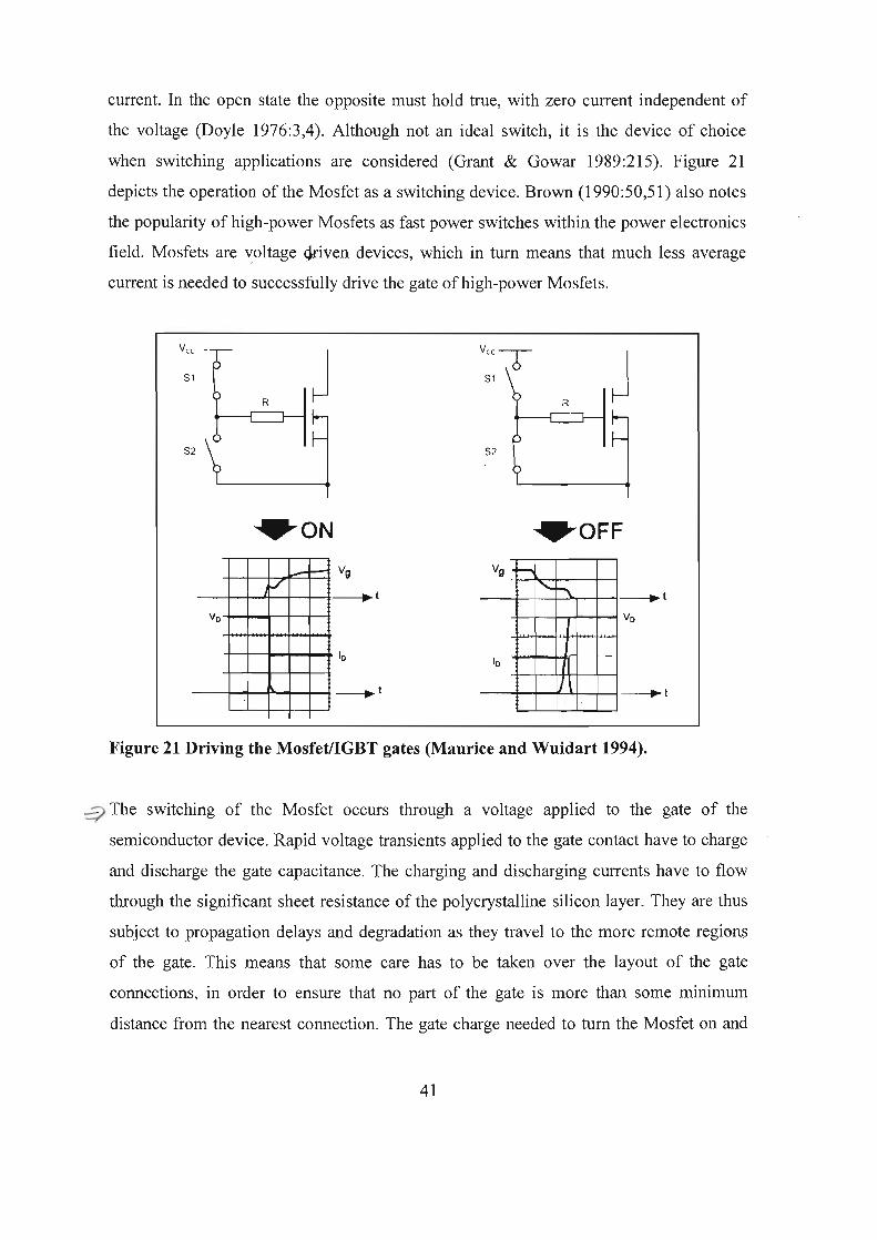
depicts the operation of the Mosfet as a switching device. Brown (1990:50,51) also notes
the popularity of high-power Mosfets as fast power switches within the power electronics
field. Mosfets are voltage 9fiven devices, which in turn means that much less average
current is needed to successfully drive the gate of high-power Mosfets.
Vcc T S1
S2
-....oN I.--1-- Vg ~
../ ......... "\. ~~
Vo
lo lo
______..I IH ~I
Figure 21 Driving the Mosfet/IGBT gates (Maurice and Wuidart 1994).
~The switching of the Mosfet occurs through a voltage applied to the gate of the
semiconductor device. Rapid voltage transients applied to the gate contact have to charge
and discharge the gate capacitance. The charging and discharging currents have to flow
through the significant sheet resistance of the polycrystalline silicon layer. They are thus
subject to propagation delays and degradation as they travel to the more remote regions
of the gate. This means that some care has to be taken over the layout of the gate
connections, in order to ensure that no part of the gate is more than some minimum
distance from the nearest connection. The gate charge needed to turn the Mosfet on and
41

off is insensitive to the current being switched and to the precise waveforms. A layout of
the gate connections that minimizes the polysilicon path lengths is crucial if the Mosfet is
to be activated in high-frequency operations. For efficient operation above 50 MHz, the
gate connections must be less than 1 mm apart (Grant & Gowar 1989:139-143).
The speed limitations of MOS circuits are due entirely to stray circuit capacitance and the
inability of the Mosfet to charge and discharge this capacitance (Crawford 1967:3-1 0).
Balogh (2001 :4) also makes the statement that the practical switching times of Mosfets
are at least two to three orders of magnitude longer than the theoretical switching time. In
high-speed applications then, the most important parameters are the parasitic
capacitances of the Mosfet device (Balogh 2001 :4). Intrinsic cut-off frequencies of MOS
devices themselves are in the order of 1 GHz. It could thus be said that Mosfets are not
really inherently bound to frequency limitations within the high-frequency range, because
of the absence of minority carrier transport. Two limits to high-frequency operation are
set by (Baliga 1987:300):
• The transient time across the drift region.
• The rate of charging of the input gate capacitance.
The transit time limited frequency response (fr) is a function or breakdown voltage
(Baliga 1987:300),
Where L = Mosfet channel length in )liD
d = Mosfet drift region thickness in )liD
BVpp = Mosfet breakdown voltage in V
0 0 0 0 (3 .1)
Taylor (1993:3) examines the gate control charge of a Mosfet when switched on. The
gate control charge (Qgate) may be expressed as (Taylor 1993 :3),
42

. . .. (3.2)
Where Css = the input gate capacitance of the Mosfet in pF
Vgs =the gate to source voltage V
C;ss is the sum of the real capacitance between the gate and source, Ccs, and the voltage
dependant capacitance between the drain and the gate called C0 c. The value of Vgs is a
function of the device and the voltage required to achieve full enhancement. The energy
expended in accumulating this gate charge (Egate) can best be expressed as (Taylor
1993 :3),
Egate = 0, 5 X ciss X vgs 2 J .... (3.3)
To show the overall drive efficiency then, the power consumed in the gate (Pgate) must be
considered via the equation (Taylor 1993 :4),
.... (3.4)
Where f = the input gate frequency in Hz
This power in the gate will only be dissipated within the gate structure if the gate
structure's resistance happens to be significantly higher than the drive circuit impedance.
The amount of power that will be dissipated in the gate of an IRF 140 (see annexure C for
the datasheet specifications of the IRF 140) when the gate to source voltage is 10 V and
the frequency of operation is 1 kHz is,
p gate = 0, 5x 1660x 10-12 X 102
X 1000
pgate = 83 J..LW
43

Therefore, driving high-power Mosfets at low frequencies requires only a small amount
of power, and thus a small amount of gate current. The gate charge may also be expressed
as an equation with regard to current and time (Taylor 1993 :24),
.... (3.5)
Where I = the input gate current in A
t 1 =the positive time period of the frequency ins
The ramifications of this simplified equation are extremely profound. If the circuit
designer knows the gate charge which is required by the power device and can design the
circuit in such a way as to utilize and exploit these charging characteristics, by judicious
control of the current flowing into or out of the gate terminal, it will then follow that time
being the ratio of the charge to the current, the switching times can be accurately
predicted (Taylor 1993 :24). The variation of the gate voltage with gate charge time when
considering the drain-source voltage is shown in figure 22. Applying a positive gate
voltage greater than the threshold voltage (V1) gives rise to a conducting channel between
the source and the drain. 10 represents the current that will flow through the drain for
certain load impedances and grs is the transconductance that determines the current
carrying capacity of the device (Grant & Gowar 1989:36, 68, 102)
100 v
-----Time (gate charge)
Figure 22 Gate voltage to gate charge time with varying drain-source voltages
(Grant & Gowar 1989:138).
44
A portion of the gate drive power will be dissipated in the internal resistance of the gate.
At frequencies around 100 kHz these losses are negligible, but at higher frequencies they
become significant, especially when considering frequencies in the 10 MHz range. The
internal gate losses (Pg(int)) are given by (Grant & Gowar 1989:165),
p - V X Q X f X _R_G:_:_(i-'nt)'----- W g(int) - gs gate R R
s + G(int)
Where Ra(int) = the internal resistance of the Mosfet gate in Q
Rs = the external resistance to the Mosfet gate in Q
.... (3.6)
To switch the Mosfet from the non-conducting to the conducting state, the gate-source
voltage must be raised from below to above the threshold voltage by a transfer of charge
into the gate. Turn-off is achieved by reversing the process. The manner in which the
transition takes place determines the switching performance of the device. A gate drive
circuit may generally be represented by a voltage source in series with a resistance. A
resistance may be inserted intentionally between the gate of the Mosfet and the voltage
source so as to modify the switching speed or represent the impedance of the voltage
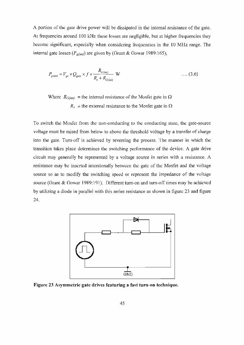
source (Grant & Gowar 1989:191). Different turn-on and tum-off times may be achieved
by utilizing a diode in parallel with this series resistance as shown in figure 23 and figure
24.
J
GND
Figure 23 Asymmetric gate drives featuring a fast turn-on technique.
45

J
GND
Figure 24 Asymmetric gate drives featuring a slow turn-on technique.
However, asymmetry may be inherent in gate drive circuits, for example when a gate
driver has an active pull down action but a passive pull up action or visa versa. Figure 25
illustrates gate drive circuits with inherent asymmetry.
vee
I GI\JD
J
GND
Figure 25 Gate drive circuits with inherent asymmetry.
To archive switching speeds of the order of 100 ns or less requires a gate drive circuit
with a low output impedance and the ability to source and sink relatively large currents.
For example, an IRF 140 will require a gate control charge of 16 nC to raise the gate
voltage from 0 to 10 V. This is calculated for an input gate capacitance of 1600 pF and a
46

gate voltage of 10 V when used in equation 3.2 (see annexure C for the IRF 140 datasheet
specifications). If the tum-on is completed within 50 ns, then the average gate current is
320 rnA from equation 3.5. A NPN and PNP transistor connected in a totem-pole
configuration as shown in figure 26, is capable of sourcing and sinking this amount of
current. It provides low output impedance, which is required by the gate of the Mosfet,
regardless of the direction of the load current (Grant & Gowar 1989: 195-196).
vee
I
Jl GND
Figure 26 Complementary emitter follower, low impedance gate drive circuit.
According to Brown (1990:51), the attainment of a saturated drain to source voltage
requires a gate voltage of at least 10 V. However, switching the Mosfet quickly on and
off may require an ampere or more of peak current. This means that the driver should be
a low-impedance active pull-up/pull-down type driver, such as the totem-pole driver
comprising a complementary emitter follower. This totem-pole driver should have a
solid, well-bypassed voltage supply in order to sink and source relatively high peak
currents. Attaining switching speeds around 30 to 50 ns should not be too difficult with
this type of driver (Brown 1990:52). However, Grant and Gowar (1989: 194) warn about
raising the gate voltage too high and thus make a recommendation to keep the gate
voltage to a maximum of 15 V, so as to maintain the reliability of the power Mosfet.
47

High-power Mosfets may also be directly driven from CMOS IC' s. The output
characteristics of CMOS are approximately the same whether sourcing or sinking current.
The main advantage is that the supply voltage may be set at 15 V, which is just what is
needed to switch the power Mosfets on and off. Lower output impedance can be achieved
by connecting a number of CMOS gates in parallel as shown in figure 27. Higher
switching times can also be achieved by the incorporation of a buffer made up of a
complementary emitter follower (Grant & Gowar 1989:203-204).
lf GND
Figure 27 CMOS output paralled to increase drive capability.
Switching a high-power Mosfet may also be achieved by using a photovoltaic isolator as
shown in figure 28. Output voltage may be 10 V while the output current will be around
50 11A maximum. It follows then that the switching frequency will be limited to around 2
kHz or less (Taylor 1993:34).
J
GND
Figure 28 A photovoltaic isolator used as a simple gate drive circuit.
48

If it is desirable to include some type of protection, Taylor (1993:35) suggests using one
of the many Micropower or CMOS linear integrated circuits. The only additional
required component will be a moderately low impedance turn-off circuit, to prevent
accidental tum-on by applied dv/dt. In the circuit layout of Mosfet gate drives, it is good
to keep the following three points in mind (Taylor 1993:60):
• Maintain all conductor lengths as short as is physically possible in order to reduce
the levels of stray capacitance.
• Currents in all conductors should be maintained as continuous, if possible, with a
small ripple component.
• Gate circuit return leads should connect directly to the source terminal of the
Mosfet package in order to eliminate the effects of feed-back from the source
inductor.
3.3 The voltage amplification and gate drive sections
Amplification of high-frequency signals has always posed a challenge to researchers the
world over. Common methods include among others Class A and Class C amplifiers.
These circuits are not ideal as they operate over a relatively narrow bandwidth. The
bandwidth required in this case is 7,950 MHz, being from 50 kHz up to 8 MHz. The ideal
waveform required in the successful gate drive of high-power Mosfets is a square
waveform, switching the Mosfet either on or off. A circuit that would thus operate
successfully across this 8 MHz bandwidth and provide a very close replica of a square
waveform is the CMOS based 40106, a HEX inverting Schmitt trigger containing 6
separate invertors. The logic diagram of one of the 6 invertors contained in the 401 06
package is shown in figure 29.
Figure 29 Logic diagram of a single inverter within the 40106.
49

From the datasheet specifications (Annexure D), it can be seen that the 40106 output
transition time from low to high is typically around 60 ns when fed from a 5 V source.
High to low transition time is typically also 60 ns. As the supply voltage increases, these
transition times decrease, thus increasing the maximum allowable clock frequency that
can be handled by the 40 l 06. A 5 V supply will cause the 40106 to successfully
accommodate a frequency of around 8 MHz that is a 120 ns time period, which then
accords to the sum of the low-to-high and high-to-low transition times of 60 ns each. The
Schmitt trigger action is mainly responsible for this transition time as well as for
relatively high input noise immunity. The 40106 will also thus provide a close replica of
the required square waveform as it switches between VCC and ground continually. The
output peak-to-peak voltage is thus a function of the supply voltage to the chip, which
can be anything between 5 and 1 5 V.
A buffer circuit comprising a complementary pair of NPN and PNP transistors has been
presented in chapter 2 as an ideal circuit to connect Mosfet gates to frequency generation
circuits. Due to their very low output impedance and excellent current sourcing, they
provide the necessary switching conditions for the gate of high-power Mosfets.
3.4 The design process of the Mosfet driver stage
Connecting multiple 40106 circuits together in series, each operating at different supply
voltages, will result in voltage amplification from 5,5 V to 12 V. This will then be
incorporated into the design to provide the necessary 12 V peak-to-peak voltage signal
needed to successfully drive the gate of a high-power Mosfet. Signal conditioning
between the 40106 voltage amplification section and the gate of the Mosfet will take
place via the use of a complementary emitter follower. Both a simulated and
experimental model will be employed in the design process of the gate drive section.
From the datasheet specifications of the 40106 (Annexure D), the hysteresis voltage is
found to be 0,5 V for a voltage supply of 5 V. The minimum input voltage level required
50

to switch the output of the 40106 low is typically 2 V. To switch the output high will thus
require an input voltage of 0,5 V less than the 2 V, which equates to 1,5 V. Figure 30
shows the input switching waveform required by the 40106, where V P represents the
positive going input threshold voltage, VN the negative going input threshold voltage and
VH the hysteresis voltage. The output from the frequency synthesizer is 5,5 V, which
should mean theoretically that only one 40106 supplied with 15 V would be necessary as
the minimum input switching levels, according to the datasheet specification, are set at 4
and 4,9 V. However, this was not found to be the case. The typical values have to be
considered, especially when operating at 8 MHz. Thus a typical value of 4,5 V is
necessary to switch the output high, and a value of 5,8 V to switch the output low when
operating at a 10 V supply. This is just out of reach from the frequency synthesizers 5,5
V maximum voltage. So by making the supply voltage to the first 40106 8 V, it is
possible to switch successfully between ground and vee when supplied with an input
voltage of either ground or 5,5 V.
Figure 30 Switching input characteristics of the 40106.
Using just one inverter on the 401 06 does not provide sufficient drive to the following
inverter in the circuit. It was found that by paralleling 3 inverters on the chip resulted in a
lower output impedance, thus providing sufficient energy for the next set of inverters,
exactly as foretold by Grant and Gowar (1989:204). The supply voltage cannot yet be set
to 15 V, as the required switching input voltages are 6,5 V and 8,3 V, and the maximum
output from the first set of inverters is not quite vee, but rather 7,425 V. Thus a second
set of inverters on a second 40106 is fed from a 9 V supply and this improves the output
switching voltage range between Ground and 9,015 V. This range between ground and 9
51

V was found though to be insufficient to drive the next stage of inverters when placed at
a 15 V supply. A 11,4 V supply was thus utilized, which accepted the 9 V maximum
input voltage signal and increased it to 11,43 V. This signal level of 11,4 V could now be
passed to the fourth and final set of inverters operating at 12 V. The 3 inverters on each
40106 thus provide voltage amplification to the next set of inverters. Four identical
inverter sets were thus used to increase the frequency synthesizer's voltage from 5,5 V to
7,425 V, then to 9,015 V, then to 11,43 V and then finally to 12,04 V. Figure 31
illustrates the four identical inverter sets on individual HEX inverter Schmitt triggers
which serve as the voltage amplification section.
From Frequency
Generation Stage
To Gate
Drive Section
Figure 31 Four 40106's connected in series which provide the voltage amplification
of a square wave.
The output from the final 40106 is passed to a complementary emitter follower via a
small value resistor and DC de-coupling capacitor. The main reason for this
complementary emitter follower is to accommodate the high-frequency signal between
the voltage amplification section and the Mosfets gate. The 40106 will not be able to
supply sufficient drive to the gate of the Mosfet to switch it either completely on or off.
By utilizing the complementary emitter follower, the gate of the Mosfet is shorted either
to VCC or to ground, which are the two ideal switching conditions for successful high
power Mosfet operations. The supply voltage to the complementary emitter follower is
set at 15 V. Two complementary emitter followers are utilized. One incorporates small
signal transistors capable of sourcing 0,5 A, and the other one uses large signal transistors
52

capable of sourcing 1,5 A. The aim of this design was firstly to provide further isolation
between the Mosfet gate and the voltage amplification section and secondly to ensure that
the peak currents through the gate of the Mosfet does not destroy the small signal
transistors that are incapable of sourcing these high currents. Figure 32 shows the two
complementary emitter followers connected in series. The inclusion of the series inductor
is to damp oscillations that occur in the output of the Mosfet as it passes through the
linear regions. It must also be remembered to couple suitable bypass capacitors onto the
supply rails of both complementary emitter followers. These bypass capacitors must be
situated as close as possible to the individual buffers, so as to source and sink relatively
high peaks of current that will pass through the complementary emitter section. Allowing
the gate of the high-power Mosfet to float when the device is connected across the supply
rails proves detrimental. It is for this reason that R18 is included in the circuit design.
From Voltage
Amplification Section
T1 Be639
T2 Be640
vee- 15V
G~ID
T3 TIP31e
T4 TIP30
Figure 32 The complementary emitter followers connected in series.
To the Gate
ofthe Mosfet
The complementary emitter follower was also simulated via the SIMETRIX simulation
software package. Figure 33 shows the simulated package's circuit diagram. The first
complementary emitter follower uses aBC 639 and BC 640. The second complementary
53
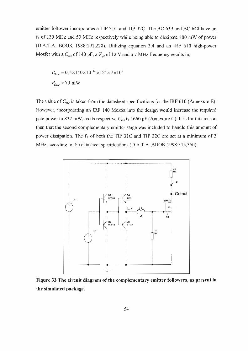
emitter follower incorporates a TIP 31 C and TIP 32C. The BC 639 and BC 640 have an
fr of 130 MHz and 50 MHz respectively while being able to dissipate 800 m W of power
(D.A.T.A. BOOK 1988:191,220). Utilizing equation 3.4 and an IRF 610 high-power
Mosfet with a Css of 140 pF, a Vgs of 12 V and a 7 MHz frequency results in,
PGale = 0, 5 X 140 X 1 o-' 2 X 122
X 7 X 106
PGale = 70 mW
The value of Css is taken from the datasheet specifications for the IRF 610 (Annexure E).
However, incorporating an IRF 140 Mosfet into the design would increase the required
gate power to 837 m W, as its respective Css is 1660 pF (Annexure C). It is for this reason
then that the second complementary emitter stage was included to handle this amount of
power dissipation. The fr of both the TIP 31 C and TIP 32C are set at a minimum of 3
MHz according to the datasheet specifications (D.A.T.A. BOOK 1998:315,350).
I V1
~ ;c tB t-output
IRF6~
_A~·--tlt--_ _,_~ L1 01 1
1k R2
I
I
Figure 33 The circuit diagram of the complementary emitter followers, as present in
the simulated package.
54
The supply voltage was initially set to 15 V. The input signal to the ftrst complementary
emitter stage was a 7 MHz 12 V peak square wave. A 50 % duty cycle was utilized with
the total time period being 143 ns.
3.5 Summary
This chapter has focused on the ampliftcation of the 5,5 V output signal of the frequency
synthesizer in chapter 2. The voltage amplification section consists of 4 series connected
HEX Schmitt triggers in package type 40106. Each set of inverters increases the voltage
level by about 1,2 V so that the final output voltage swing is from ground to 12 V, at the
maximum operating frequency of 8 MHz.
The final section, before connecting to the gate of the high-power Mosfet, consists of two
complementary emitter followers connected in series. These two buffers provide the
necessary impedance and current sourcing required by the gate of the Mosfet.
Chapter 4 will present the results obtained from the frequency generation stage as well as
the results measured from the voltage amplification section and complementary emitter
followers that serves as the Mosfet driver stage. Measured waveforms obtained at
specific points on the final circuit board will be presented. The final circuit layout as well
as the final printed circuit board will also be considered.
55

Chapter 4 The results
4.1 Introduction
Chapter 4 considers the measured results, in both time and frequency domain, of the
completed high-frequency Mosfet driver. The simulated and experimental results of the
complementary emitter circuit utilized in the high-frequency Mosfet driver section will
also be presented. The measurements were obtained via the PI CO-SCOPE ADC 2001100
spectrum analyser and the TEKTRONIX 100 MHz Digital Storage Oscilloscope.
4.2 The results of the high-frequency generation stage
The frequency generation stage comprises the PLL, programmable divider and frequency
reference sections. These sections are present in figure 35 where the final circuit diagram
with all relevant test points are shown. Figure 34 is obtained from test point A and
illustrates a 7 MHz PLL output frequency.
v 5
4
3
x=-2672mV,o=2414mV,xo=5086mV
:---r------- _L~ ----
:: I -~------4
-5 ns
800 840 880 920 960 1000 1 040 1 080 1120 1160 1200
ch A: Frequency (MHz) ch A: Duty cycle(%) ch A: Risetime (ns) ch A: Falltime (ns)
07Nov2003 13:01
7.027 51.35 17.86 17.86
Figure 34 The 7 MHz output frequency signal taken from test point A.
56
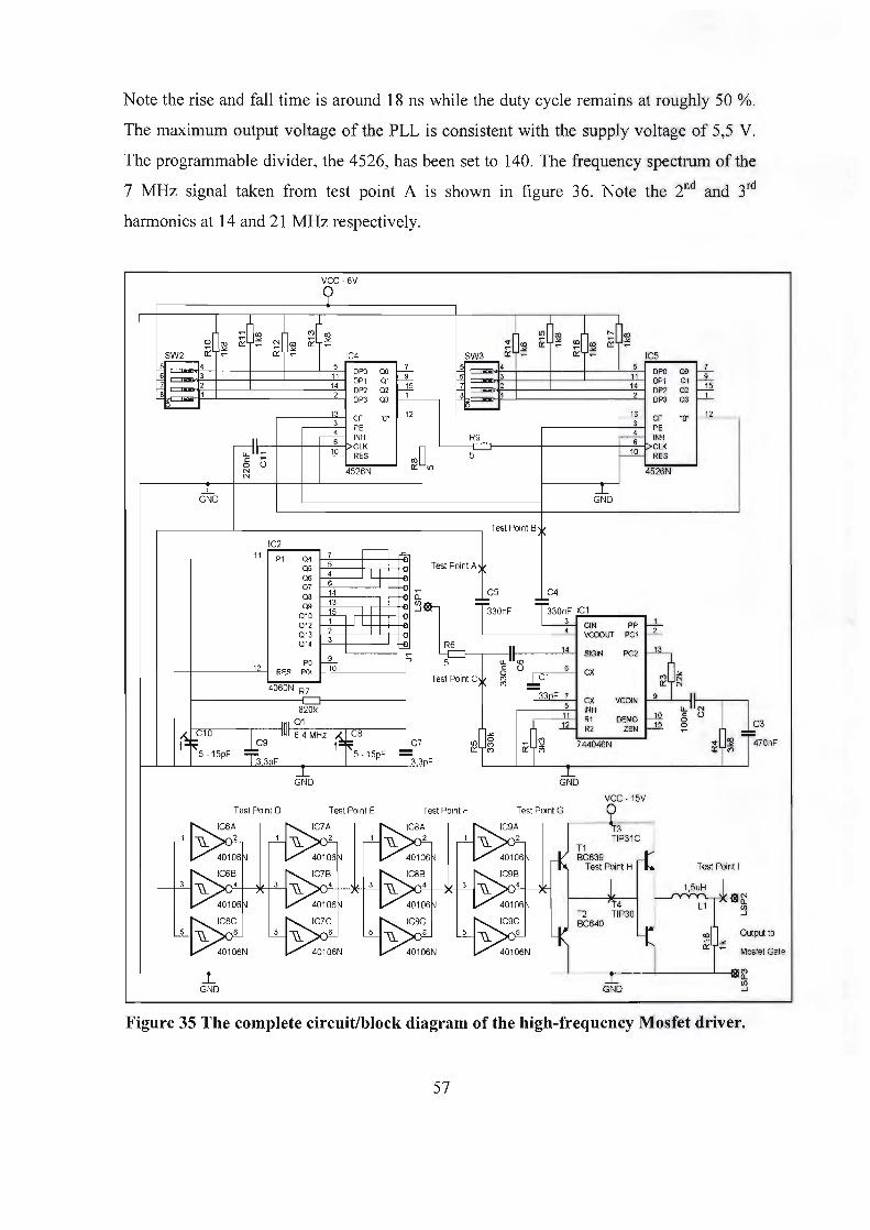
Note the rise and fall time is around 18 ns while the duty cycle remains at roughly 50 %.
The maximum output voltage of the PLL is consistent with the supply voltage of 5,5 V.
The programmable divider, the 4526, has been set to 140. The frequency spectrum of the
7 MHz signal taken from test point A is shown in figure 36. Note the 2nd and 3rd
harmonics at 14 and 21 MHz respectively.
VCC-6V
9
::I ~ dco "' co " ]co 0 co
N J~ ~ "' ... 0:: ~ <0 ~ "' a:: a:: ~
~ co a:: ~
0:: ~~ ~ "' 0:: 0:: ~ SW2 a:: ~ IC4 SW3 IC5 5 =- 4 5 DPO QO ~ ~ c:::Ji<iil 4 5 DPO QO ~ 6 3 11 DP1 01 +s !..§ =- 3 11 DP1 01 +s 7 2 14 DP2 02 2 14 DP2 02 B 1 2 I-f ~~1 2 ~ ~
DP3 03 DP3 03
13 r-11- 13 12 3 CF "0" 3
CF ·o-
~ PE
----4-PE
~L INH R9 INH 6 CLK
~L 6 CLK
" ~ c--1Q- RES 5 __1Q_ RES
0 0 4526N 4526N N
N
dJo dJo Test Point B
IC2 II"'= 11 P1 04 7
5
~ Q5
4 ~ Test Point A
06 6 ~~ 07 14 C5 C4 Q8 13 _rr~ ~~. ==330nF : :330nF IC1 Q9
+t-r 010 012 ______L GIN pp --J-013 Lr-~ 4 VCOOIJT PCI ...2_
3 014 ~~ R6 II 14 __!.L
+a u.llco SIGIN PC2
PO ...,
5 12 RES PO\ " 0 6 ~ J:C1 ex "2[ "' Test Point C a:: f::
4060N ~ T33pF 7 ex VCOIN 9 Ill
s2oi< u.IIN 11 R1 DEMO ~
II' 01
~ C10 II-II 6 4 MHZ '1~8 1:: C9 ' C7 ~5 -15pF
t !:: 3 30
F 5- 15pF T33pF
5 I INH
~[ E._ R2 "' "'
0 ~ ~ 744046N a:: ~ a:: "'
ZEN ~ 8 0
... Jf == a:: "'
C3
470nF
dJo dJo Test Point D Test PointE Test Point F Test Po1nt G
9c 15V
~ ~ ~ ~ " ~ TIP31C 2
T1 2 2 2
~ ~ ~ 6~ BC639 Test Point H Test Point I
~e IC7B ICBB IC9B
J - .,.._4 3 \1. 4 3 \1. .r-.4 3 \1. .,.._4 1,5uH J, ~~06~
·~ ~ -~ ~~N 40106~ 40106~ 40106 ~ :::~30 L 1 S;
T2 ..J
6 6 6 6 co Out ~ 6N ~ N ~ N
l,~ 6N ~ ~·" l 0:: ~
put to
fetGate Mas
...L GND
...L GND
"""' -a. lfl ..J
Figure 35 The complete circuit/block diagram of the high-frequency Mosfet driver.
57

dB
30 7 MHz fundamental
20 l 2nd Harmonic
3rd Harmonic 10
0
-10
-20
-30 h I !I ,\JUlruv· MHz
0 5 I 0 15 20 25 30 35 40 45 ch A: Frequency At peak (MHz) 7.038
17May2004 0 I :06
Figure 36 Frequency spectrum showing a 7 MHz frequency signal.
v 10
8
6
x=-2i56mV, o=2760mV,xo=5516mV
50
_t'v ---- _\____ -l--1 -- ---~/-~- - ------,-/~- - ---- _d __ _
-4
-6
-8
-10 ns 800 840 880 920 960 1000 1040 1080 1120 1160 1200
ch A: Frequency (MHz) 8.021 ch A: Duty cycle(%) 50.80 ch A: Risetime (ns) 25.62 ch A: Falltime (ns) 25.00
07Nov2003 11:30
Figure 37 Maximum possible output frequency of 8 MHz obtained at test point A.
The maximum possible output frequency of the frequency generation stage measured via
the digital oscilloscope at test point A is shown in figure 37. This 8 MHz output
58

frequency is accomplished by setting the dip switches on the divider circuit (the CMOS
4526) to divide by 160. Note that the output voltage remains around 5,5 V peak-to-peak
while the rise and fall times are roughly 25 ns each. The duty cycle remains at 50 %.
These values for rise and fall time as well as for duty cycle and peak-to-peak voltage
remain more or less constant across the entire frequency range from 8 MHz down to 50
kHz. Figure 38 illustrates the 50 kHz output frequency measured at pin 9 of the 74HC
4046. The division factor on the dip switches connected to the divider section, the two
4526's, is set at 1, since both the reference frequency and output frequency are 50 kHz.
v 5
4
2
0
-1
-2
x=-2591 mV,o=2789mV,xo=5380mV
- - - - - ,.......,..li!MI_IIIt- - - - - -~l!oo¥-,....Mil- - - - --
----............... _---- .,.._....., ___ ------------3
-4
-5 25 30 35 40
ch A: Frequency (kHz) ch A: Duty cycle(%) ch A: Risetime (ns) ch A: Falllime (ns)
45 50 55
17May2004 01 :02
60
50.03 49.17 15.00 16.00
65 70 i.JS
75
Figure 38 Minimum possible output frequency of 50 kHz obtained at test point A.
Figures 39 and 40 show the output frequency spectrum of the 74HC 4046 as seen via the
digital spectrum analyser. The odd harmonics of the 8 MHz signal are evident in figure
39 while figure 40 highlights the harmonics ofthe 50 kHz minimum output frequency. A
significant observation is that the amplitude level of both the 50 kHz and 8 MHz signals
are roughly constant at 10 dB. This was also verified by the digital oscilloscope readouts
as shown in figure 37 and figure 38, where the average peak-to-peak voltage remained at
around 5,5 V, independent of frequency change.
59
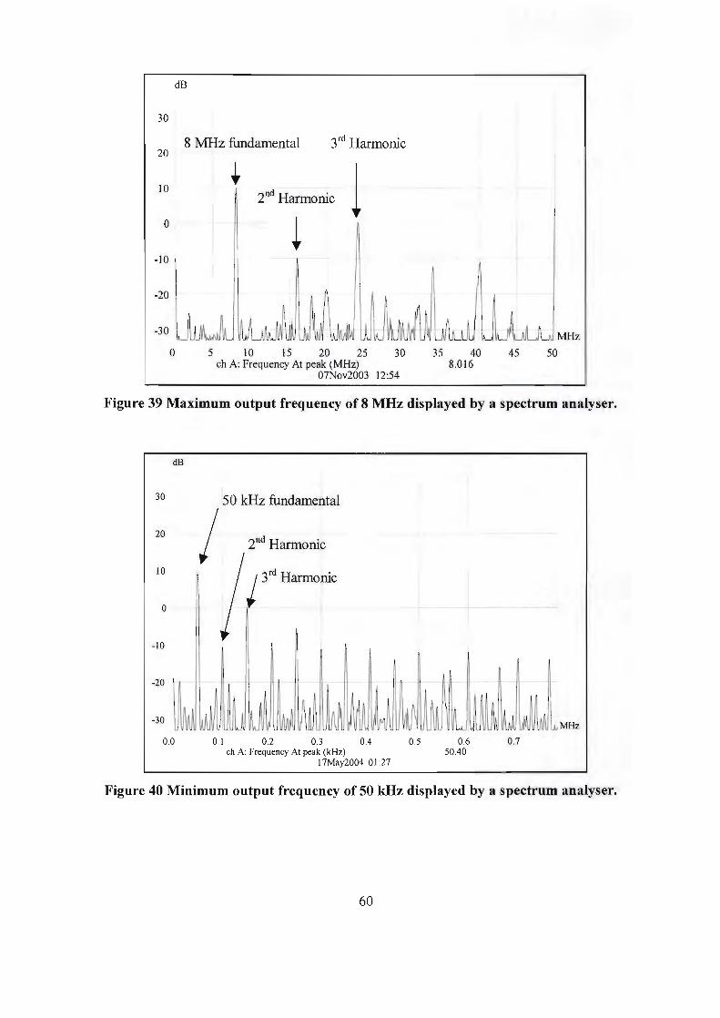
dB
30
8 MHz fundamental 3rd Harmonic 20
10 2nd Harmonic 1
0
-10
::: lkJJlLA 0 5 10 15 20 25 30
ch A: Frequency At peak (MHz) 07Nov2003 12:54
JnuJ MHz 35 40 45 50
8.016
Figure 39 Maximum output frequency of 8 MHz displayed by a spectrum analyser.
dB
30
20
10
0
-10
-20
-30
0.0
50 kHz fundamental
I 2"" Harmonic
j 3"' Harmonic
0. I 0.2 0.3 0.4 0.5 ch A: Frequency At peak (kHz)
I 7May2004 0 I :27
0.6 50.40
0.7
Figure 40 Minimum output frequency of SO kHz displayed by a spectrum analyser.
60
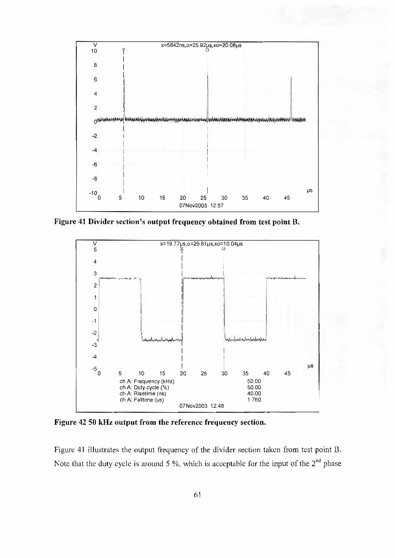
v x-5842ns,o=25.929s,xo-20 .08~s 10 ¥
I I 8 I I
6 I
4
2 "" ... L I
0~ .a.J .. "' "''·" ..... ~~~~:'"" I I
-2 I I I I
-4 I I I I
-6 I I -8 I I
I I -10 I I
0 5 tO 15 20 25 30 35 40 45
07Nov2003 12:57
Figure 41 Divider section's output frequency obtained from test point B.
v 5
4
3
2
0
-1
-2
-3
-4
-5 0
x=19.77~s.o=29.81 ~s.xo=1 0.04~s
1 9 I I I I I I
~~--li.....r-l I I I I
'I I
j I I
~""'.{~ : ..... ~....W....J.o,.,J,.
r·,.'ll'~~--
I I I I I I
5 10 15 20 25 30 35 40 45
ch A: Frequency (kHz) ch A: Duty cycle(%) ch A: Risetime (ns) ch A: Falltime (us)
07Nov2003 12:48
50.00 50.00 40.00 1.780
Figure 42 SO kHz output from the reference frequency section.
~s
~s
Figure 41 illustrates the output frequency of the divider section taken from test point B.
Note that the duty cycle is around 5 %, which is acceptable for the input of the 2nd phase
61

comparator circuit in the 74HC 4046. This is because it makes use of 0-type flip-flops
that are positive-edge triggered devices. Other circuits will not be as lenient, and thus
some type of signal conditioning will have to be performed. For instance, the reference
single input circuitry of the 74HC 4046 will not function correctly if supplied with such a
5 % duty cycle signal. It is thus for this reason that the reference frequency is taken from
pin 6 of the 4060, which provides a exact 50 % duty cycle as shown in figure 42. Figure
42 is the resulting signal from test point C. This is derived from a 6,4 MHz quartz crystal
connected across pins 10 and 11. This 6,4 MHz frequency signal is then divided by a
factor of27 to give 50 kHz.
4.3 The results of the Mosfet driver stage
The Mosfet driver stage comprises a voltage amplification and gate drive section. The
voltage amplification section consists of 4 CMOS HEX inverters, where 3 inverters on
each IC are paralled. The outputs of each of the 4 CMOS HEX inverters, obtained from
test points D through G (see figure 35), are shown in figures 43 through 46 respectively.
v 10
8
6
4 ____ _
2
0
x=-3789mV,o=3636mV,xo=7 425mV
-~------ ------ ---~
:~---- --- --6
-8
ns -10
800 840 880 920 960 1 000 1 040 1 080 1120 1160 1200
ch A: Frequency (MHz) ch A: Duty cycle(%)
13Nov2003 08:57
6.989 51.89
Figure 43 The first 40106's output within the voltage amplification section.
62

v 10
8
4
2
0
-2
-4
-6
-8
-10 800
x=-3333mV,o=5682mV,xo=9015mV
\ ~ ~~~~~'\- -~~~ - \ \ J \ '
------ -~ ----- - -------
ns
840 880 920 960 1000 1040 1080 1120 1160 1200 ch A: Frequency (MHz) ch A: Duty cycle(%)
13Nov2003 08:56
6.989 43.01
Figure 44 The second 40106's output within the voltage amplification section.
v 10
8
6
4
2
0
-2
-4
-6
-8
-10 800
x=-6287mV,o=5152mV,xo=11.43V
------r~
~-- -~~~~~~~~--ns
840 880 920 960 1000 1040 1080 1120 1160 1200 ch A: Frequency (MHz) ch A: Duty cycle(%)
13Nov2003 08:56
7.035 53.27
Figure 45 The output of the third 40106 within the voltage amplification section.
63

v 20
16
12
8
4
0
-4
-8
-12
-16
-20 800
x=-2459mV,o=9590mV,xo=12. 04V
ns
840 880 920 960 1 000 1 040 1 080 1120 1160 1200
ch A: Frequency (MHz) ch A: Duty cycle(%)
13Nov2003 08:55
7.027 34.05
Figure 46 The output of the fourth 40106 within the voltage amplification section.
The above results show that the voltage amplification section is working correctly. Each
HEX inverter does indeed provide a voltage increase of around 1 ,2 V. This then serves to
increase the output from the frequency generation stage from 5,5 V to the required 12 V
to successfully drive the gate of the high-power Mosfet. The output frequency spectrum
from the last inverter IC, the 40106, of the amplification section is shown in figure 47.
The 2"d harmonic component is very evident at 14 MHz, while the third harmonic
component has fallen somewhat. Recall from figure 36 that the output from the PLL for a
frequency of 7 MHz contained a higher third harmonic component than the second
harmonic component. The amplification section utilizing the four 40106 HEX inverters
seem to reverse this phenomena and provide more amplification to the second harmonic
component than to the third, as seen in figure 4 7. This frequency signal is now passed to
the complementary emitter follower. Figure 48, taken from test point H in figure 35,
portrays the output of the first complementary emitter follower that functions as the first
buffer. The output voltage of the complementary emitter follower remains at 12,04 V,
although the duty cycle is significantly less than 50 %. The output from the second buffer
(figure 49) was obtained at test point I, when connected to the gate of the high-power
64
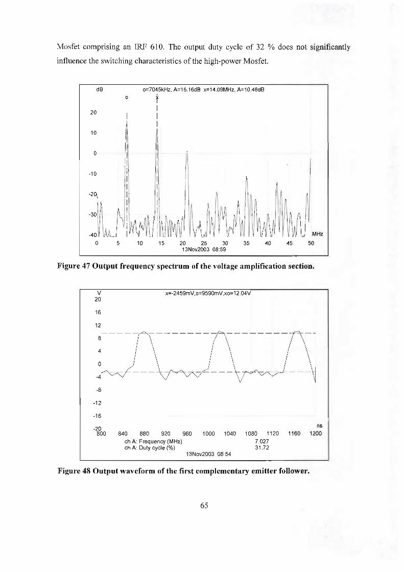
Mosfet comprising an IRF 61 0. The output duty cycle of 3 2 % does not significantly
influence the switching characteristics of the high-power Mosfet.
dB
20
10
0
-10
-2
0 5
~ I I
10
o=7045kHz, A=15.16dB x=14 .09MHz, A=1 0.46dB
f I I I
15 20 25 30 35 13Nov2003 08:59
r\ ~ \N u MHz
40 45 50
Figure 47 Output frequency spectrum of the voltage amplification section.
v 20
16
12
8
4
0
-4
-8
-12
-16
-20 800
x=-2459mV,o=9590mV,xo=12.04V
ns
840 880 920 960 1 000 1040 1 080 1120 1160 1200
ch A: Frequency (MHz) ch A: Duty cycle(%)
13Nov2003 08:54
7.027 31.72
Figure 48 Output waveform of the first complementary emitter follower.
65

v 20
16
12
8
4
0
""""-~-- --4 'V ,, v--8
-12
-16
x=-2459mV,o=9590mV,xo=12.04V
- :::J
ns -20 800 840 880 920 960 1 000 1 040 1 080 1120 1160 1200
ch A: Frequency (MHz) ch A: Duty cycle (%)
13Nov2003 08:53
7.179 32.82
Figure 49 Output waveform of the second complementary emitter follower.
The effect of the complementary emitter follower on the gate of a high-power Mosfet was
also investigated by means of a simulated model. Figure 50 shows the simulated model ' s
result. Signal A represents the input signal to the Mosfet gate while signal B represents
the output of the high-power Mosfet. The input voltage signal of 12 V, supplied by the
complementary emitter follower, successfully switches the 15 V supply that is across the
Mosfet. The frequency of operation was also calculated as 7 MHz, from the resulting
time period. The simulated model ' s result for input signal to output signal for the Mosfet
was then compared to the experimental models result. The experimental model's result is
shown in figure 51, where the gate input signal and drain output signal are shown. Refer
to figure 33 for this test point's location in the circuit. Comparing figures 50 to 51 yields
no real significant differences except for the waveform shapes. Signal voltages and
switching times are similar for both the simulated and experimental models. A
comparison was also made between the outputs of the complementary emitter follower
when connected to and when isolated from the gate of the high-power Mosfet. Figure 52
illustrates this comparison.
66

3.91!Slip 143.822511 ~--143.818flns8flns----)
B !;1 i I V1 ~) /
A "' "' ! ; •• 1"--. ) \ I I
11.898623
11.878704'1
\
\ L ____ \_ J
..., \. 1 j \ ---- - ,-- -- --- ~ .,.------- - 1>-- ------ liS --- - - ---- 19.918EOn -
Figure 50 The simulated models result of the high-power Mosfet where; A- is the
input to the Mosfet gate and; B- is the output from the Mosfet drain.
Figure 51 The input and output of the high-power Mosfet according to the
experimental model.
No significant differences exist except for the zero voltage of the isolated gate being
smoother than that of the connected gate. This is due to the influence of the gate
67

capacitances on the input voltage signal from the complementary emitter follower. The
differences between the output voltage signals of the experimental and simulated models
were investigated and are depicted in figure 53. Once again no significant differences
exist, except for the experimental models flatter top voltage response.
l) [S¢ope}. · · · : · · · 2J rs~op'el
. . . .
.. ''\ . : : \ :
.. "" ~· ... : .. y.··:···-,.\.~ ·: ··· . . . . . . ..
X . . . . . . . . .
5 y 45 n$ · ·s·v· · ·25ns; · · · ·: · · ·
. . . . . . ... . .. . . . . . . . . . . . . . .
Figure 52 The output of the complementary emitter follower when; X- isolated
from the Mosfet's gate and; Y- connected to the gate of the high-power Mosfet.
. . -. . -. . -. . ..... . .. ... . J . : .... : .... : . .. ..:
t • • I . -.. . I
Figure 53 The simulated and experimental models result.
68
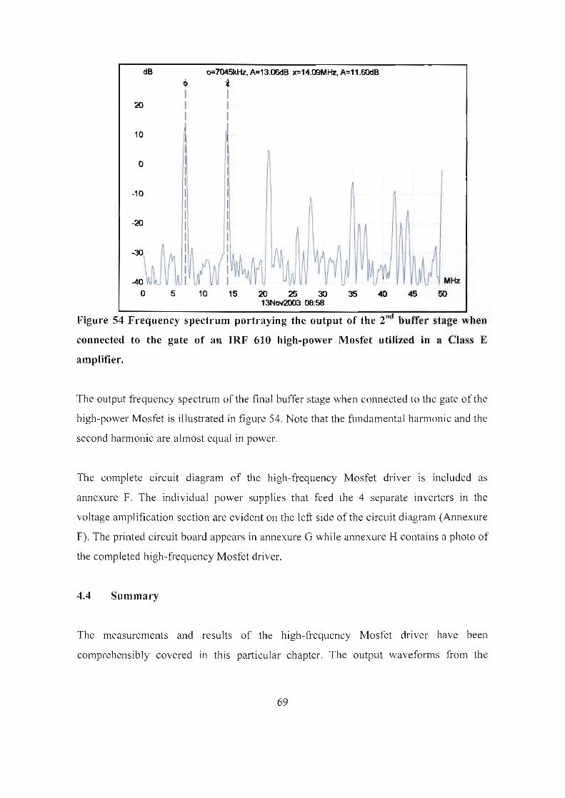
dB
20
10
0
-10
-20
0 5
~ I I I
o=7045kHz, A=13.06dB x=14.09MHz, A=11.60dB
* I I I
10 15 20 25 30 35 13Nov2003 08:58
45
MHz
50
Figure 54 Frequency spectrum portraying the output of the 2"d buffer stage when
connected to the gate of an IRF 610 high-power Mosfet utilized in a Class E
amplifier.
The output frequency spectrum of the final buffer stage when connected to the gate of the
high-power Mosfet is illustrated in figure 54. Note that the fundamental harmonic and the
second harmonic are almost equal in power.
The complete circuit diagram of the high-frequency Mosfet driver is included as
annexure F. The individual power supplies that feed the 4 separate inverters in the
voltage amplification section are evident on the left side of the circuit diagram (Annexure
F). The printed circuit board appears in annexure G while annexure H contains a photo of
the completed high-frequency Mosfet driver.
4.4 Summary
The measurements and results of the high-frequency Mosfet driver have been
comprehensibly covered in this particular chapter. The output waveforms from the
69

frequency generation stage incorporating the 74HC 4046 PLL, 4526 divider and 4060
ripple counter have been presented. The results of the voltage amplification section and
complementary emitter follower have also been discussed. The final waveforms from
across the IRF 610 Mosfet indicates the successful switching of the Mosfet at 7 MHz.
This has been confirmed by both the experimental and simulated models resuhs. Swart
and Pienaar (2004) presented the experimental results at the SAUPEC 2004 conference
held at the University of Stellenbosch, South Africa. Swart, Pienaar and Case (2004)
furthermore presented the simulated results of the gate drive circuit at the AFRICON
2004 conference held in Gaborone, Botswana.
The final chapter of this research project, chapter 5, will consider the conclusions reached
with regard to the design and development of the high-frequency Mosfet driver.
Recommendations as to future research on high-frequency Mosfet drivers will also be put
forward.
70
Chapter 5 Conclusions and recommendations
5.1 Introduction
The final chapter of this research document presents the conclusions reached with regard
to the design and development of a high-frequency Mosfet driver. The original purpose
will be reviewed together with the final results of the high-frequency Mosfet driver.
Recommendations for future research will conclude this chapter.
5.2 Conclusions
One of the most notable conclusions that can be made from this project is the flexibility,
efficiency and reliability of the PLL circuit. A number of prototypes were manufactured ~ <:( .
in the design and development of the fr~qnmey ~ener~n stage. Each of the prototypes, v0 1
while not functioning according to ex ectation, produced a stable output freLJ.uency based \)')
on an equally stable input Y.€qUency. The lock range, of the first prototype, was found to
exisrl5etween 98kHz and 1,144 MHz, when utilizing a timing capacitor, C1, of 180 pF.
See figure 3 5 for C 1 's position. At this time only a single capacitor, C2, was being
utilized in the low-pass filter configuration. It was found that a smaller loop filter
capacitance of 15 pF used in conjunction with phase comparator 1 would result in a
smaller amount of VCO output frequency variations. A wiring error had though occurred
between the PLL and divider section that was rectified in the second prototype.
The second prototype would though only operate between 200 kHz and 800 kHz. The
value of C 1 had remained constant but the value of the loop filter's capacitor had
changed to 100 nF. The reason for making the ]oop filter's capacitor larger was that,
although variations within the output frequency range where being combated with lower
values of C2, the lock range was being lowered and high output frequencies were not
being produced. Phase comparator 1 was still being utilized, as it was desired to have the
free-rurming frequency at the middle of the lock range when no input signal was
available. Now with the low-pass filter set at 100 nF, oscillation in the order of 3 kHz
71
readily occurred at higher frequencies of 500 kHz and above. This is where Lythall's
(2002: 1) design was utilized incorporating a paralleled resistance and capacitance in
series with a single capacitor to ground. A 470 nF capacitor was paralled with a 3,3 H2
resistor and a 100 nF capacitor in series to ground. All oscillations stopped and a perfect
square wave originated at the output with no visible distortions. Frequency lock was
achieved much quicker, with no excess drifting of the locked frequency. Thus, it can be
concluded that an existing PLL circuit can be improved utilizing the improved low-pass
filter technique from Lythall (2002: 1 ). It was further decided to move to phase
comparator 2, as this would make the capture and lock range equal. It would also
eliminate the possibility of the output frequency [ocking onto the harmonics of the
reference input signal. The CMOS-based 4059 was utilized as the divider section. It is a
divide-by-N counter capable of a maximum count of 15000, but being restricted to an
input clock frequency of 2 MHz.
With the PLL circuit operating correctly, attention was then directed to a new divider
section comprising the 4526. A third prototype was developed using the specifications of
the second prototype for the PLL, but incorporating the 4526 as the divider section so as
to attain frequencies higher than 2 MHz. The third prototype was completed and tested. It
was found that the divider section was not operating correctly at frequencies above 2
MHz. A divide-by-4 prescaler was thus included into the 4th prototype. The idea was to
divide the maximum output frequency by 4, which would then result in a frequency
below 2 MHz, a frequency that the divider IC, the 4526, could accommodate. This
proved successful and the frequency synthesizer was operating correctly between 50 kHz
and 8 MHz in 50 kHz steps. Then, instead of utilizing a 5 V regulator to feed the
frequency synthesizer section, a 6 V regulator was used to feed the divider and reference
section, while a diode was added in line to the PLL circuit, so that its voltage remained at
below 5,5 V. This then enabled frequency operation upwards of 10 MHz by the divider
section, the 4526. A noteworthy deduction here is that just a half a volt increase on the
supply voltage to the 4526 makes it operate at frequencies above 2 MHz. The presca1er
could now be discarded and the final and fifth prototype could be constructed.
72

Subsequent measurements confirmed the successful operation of the frequency
generation stage. Attention was now directed at the Mosfet driver stage.
Focus was directed to the amplification ofthe 5,5 V signal received from the 74HC 4046.
It was initially assumed that the use of 4 HEX inverter IC's would increase the voltage
level of the maximum output frequency of the PLL to an acceptable level to drive the
gate of a high-power Mosfet. This was implemented and worked immediately. However,
the 40 I 06 could not provide sufficient drive to the Mosfets gate as it cannot source and
sink large amounts of peak current. Therefore, 2 complementary emitter followers were
included to source and sink the peak currents that flowed into and out off the Mosfets
gate. Results were immediately forthcoming and successful. The most notable conclusion
is that complementary emitter followers proved to be very successful in driving the gate
of the high-power Mosfets, even at high frequencies.
The original purpose to design and develop a high-frequency Mosfet driver was achieved.
The generation of frequencies between 50 kHz and 8 MHz in 50 kHz steps was
accomplished by the frequency generation stage utilizing a coherent, indirect, frequency
synthesizer. This frequency synthesizer incorporated a PLL, divider circuit and reference
frequency section. Supplying sufficient drive to the gate of a high-power Mosfet was
addressed by the use of 4 HEX inverters and 2 complementary emitter followers . The
effectiveness of the complementary emitter followers was proven both in the simulated
and experimental models.
5.3 Recommendations
A number of IC's have been developed that include both the divider and the reference
frequency section. Investigation into the possible use of these circuits in place of the three
separate sections currently used could lead to the simplification of the overall board
construction. Smaller board designs could thus be forthcoming. Utilizing the IRF 610
Mosfet accomplished the desired on and off switching time of less than 70 ns, which
equates to a frequency of around 8 MHz. However, it does not have the capability of
73

handling large amounts of power. Connecting 2 or more IRF 610's in parallel could solve
the problem of delivering larger amounts of power to the load. This aspect remains to be
investigated with regard to high-frequency Mosfet drivers.
74
References
List of sources quoted
(.) BALIGA, B.J.1987. MODERN POWER DEVICES. New York: Wiley.
• BALOGH, L. 2001. Design and application guide for high speed Mosfet gate drive
circuits. [Online]. Available at: <http://focus.ti.com/lit/ml/slup 169/slup 169.pdf>.
Accessed 1 0/02/2003.
• BERLIN, H.W. 1982. PHASE-LOCK LOOPS Theory, Design, and Applications. 5th
ed. Michigan: Heath Company.
• BEST, R.E. 1984. PHASE-LOCK LOOPS Design, Simulation and Applications. New
York: McGraw-Hill.
• BEST, R.E. 1997. PHASE-LOCK LOOPS Design, Simulation and Applications. 3rd
ed. New York: McGraw-Hill.
• BLAKE, R. 2002. Electronic Communication Systems. 2nd ed. New York: Delmar.
• BRENNAN, P.V. 1996. PHASE-LOCKED LOOPS; Principles and Practice. London:
Macmillan Press.
• BROWN, M. 1990. Practical power supply design. San Diego: Academic Press.
• BROWNE, J. 2003. Microwave & RF. [Online]. Available at:
<http://www.mwrf.com/ Articles/lndex.cfm? ArticleiD=6631>. Accessed 10/11/2003.
• CRAWFORD, R.H. 1967. MOSFET in Circuit Design. Texas Instruments Electronics
Series. New York: McGraw-Hill.
• D.A.T.A BOOK. 1988. Electronic Information Series. 24th ed. San Diego: D.A.T.A.
• DOYLE, J.M. 1976. DIGITAL, SWITCHING, AND TIMING CIRCUITS. North
Scituate: Duxbury Press.
75

• GRANT, A. D. & GOWAR, J. 1989. POWER MOSFETS Theory and Applications.
New York: Wiley.
• LYTHALL, H. 2002. CMOS RF SYNTHESIZER. [Online]. Available at:
<http://wl.859.telia.com/-u85920178>. Accessed 10/04/2003.
• MANASSEWITSCH, V. 1987. FREQUENCY SYNTHESIZERS Theory and Design.
3rct ed. New York: Wiley.
• MARSTON, R.M. 1996. Modern CMOS Circuits Manual. Oxford: Newnes.
• MAURICE, B. and WUIDART, L., 1994. Drive circuits for power Mosfets and
IGBTs. [Online]. Available at:
<http://www.st.com/stonline/books/ascii/docs/3703.htm> . Accessed on 12/05/2004.
• PHILIPS SEMICONDUCTORS. 2004. All products. [Online]. Available at:
<http://www. standard products. phi I ips .com/products/> . Accessed on 12/05/2004.
• SWART, A.J . & PIENAAR, H.C.vZ. 2004. " A high frequency Mosfet driver"
presented at the SA UPEC 2004 conference, University of Stellenbosch, Stellenbosch.
• SWART, A.J., PIENAAR, H.C.vZ. & CASE, M. 2004. "A Radio Frequency Mosfet
driver" presented at the AFRICON 2004 conference, Gaborone International
Conference Centre, Gaborone, Botswana.
• TAYLOR, B.E. 1993 . POWER MOSFET DESIGN. Chich,ester: Wiley.
• VAN ROON, T. 2001. PHASE-LOCK LOOPS. [Online]. Available at:
<http://www .uoguelph.ca/% 7Eantoon/gadgets/pll/pll .html>. Accessed 04/05/2004.
76
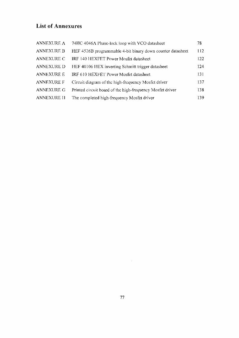
List of Annexures
ANNEXURE A 74HC 4046A Phase-lock loop with VCO datasheet 78
ANNEXUREB HEF 45268 programmable 4-bit binary down counter datasheet 112
ANNEXUREC IRF 140 HEXFET Power Mosfet datasheet 122
ANNEXURED HEF 40 I 06 HEX inverting Schmitt trigger datasheet 124
ANNEXURE£ IRF 610 HEXFET Power Mosfet datasheet 131
ANNEXUREF Circuit diagram of the high-frequency Mosfet driver 137
ANNEXUREG Printed circuit board of the high-frequency Mosfet driver 138
ANNEXUREH The completed high-frequency Mosfet driver 139
77

7 4HC 4046A Phase-lock loop with VCO datasheet ANNEXURE A
INTEGRATED CIRCUITS
For a complete data sheet, please also download:
• The IC06 74HC/HCT/HCU/HCMOS Logic Family Specifications
• The IC06 74HC/HCT/HCU/HCMOS Logic Package Information
• The IC06 74HC/HCT/HCU/HCMOS Logic Package Outlines
74HC/HCT4046A Phase-locked-loop with VCO
Product specification Supersedes data of September 1993 File under Integrated Circuits, IC06
1997 Nov 25
Philips Semiconductors 78 PHILIPS

Philips Semiconductors
Phase-locked-loop with VCO
FEATURES
• Low power consumption
• Centre frequency of up to 17 MHz (typ.) at Vee= 4.5 V
• Choice of three phase comparators: EXCLUSIVE-OR; edge-triggered JK flip-flop; edge-triggered RS flip-flop
• Excellent VCO frequency linearity
• VCO-inhibit control for ON/OFF keying and for low standby power consumption
• Minimal frequency drift
• Operating power supply voltage range: VCO section 3.0 to 6.0 V digital section 2.0 to 6.0 V
• Zero voltage offset due to op-amp buffering
• Output capability: standard
• Icc category: MSI.
GENERAL DESCRIPTION
The 74HC/HCT4046A are high-speed Si-gate CMOS devices and are pin compatible with the "4046" of the "40008" series. They are specified in compliance with JEDEC standard no. ?A.
The 74HC/HCT4046A are phase-locked-loop circuits that comprise a linear voltage-controlled oscillator (VCO) and three different phase comparators (PC1, PC2 and PC3) with a common signal input amplifier and a common comparator input.
The signal input can be directly coupled to large voltage signals, or indirectly coupled (with a series capacitor) to small voltage signals. A self-bias input circuit keeps small voltage signals within the linear region of the input amplifiers. With a passive low-pass filter, the "4046A" forms a second-order loop PLL. The excellent VCO linearity is achieved by the use of linear op-amp techniques.
The VCO requires one external capacitor C1 (between C1A and C1 6 ) and one external resistor R1 (between R1 and GND) or two external resistors R1 and R2 (between R1 and GND, and R2 and GND). Resistor R1 and capacitor C1 determine the frequency range of the VCO. Resistor R2 enables the VCO to have a frequency offset if required.
The high input impedance of the VCO simplifies the design of low-pass filters by giving the designer a wide choice of resistor/capacitor ranges. In order not to load the low-pass filter, a demodulator output of the VCO input voltage is
1997 Nov 25 2
Product specification
7 4HC/HCT 4046A
provided at pin 10 (DEMour). In contrast to conventional techniques where the DEMour voltage is one threshold voltage lower than the VCO input voltage, here the DEMour voltage equals that of the VCO input. If DEMour is used, a load resistor (Rs) should be connected from DEMour to GND; if unused, DEMour should be left open. The VCO output (VCOour) can be connected directly to the comparator input (COMP1N). or connected via a frequency-divider. The VCO output signal has a duty factor of 50% (maximum expected deviation 1 %), if the VCO input is held at a constant DC level. A LOW level at the inhibit input (IN H) enables the VCO and demodulator, while a HIGH level turns both off to minimize standby power consumption.
The only difference between the HC and HCT versions is the input level specification of the INH input. This input disables the VCO section. The sections of the comparator are identical, so that there is no difference in the SIG1N (pin 14) or COMP1N (pin 3) inputs between the HC and HCT versions.
Phase comparators
The signal input (SIG1N) can be directly coupled to the self-biasing amplifier at pin 14, provided that the signal swing is between the standard HC family input logic levels. Capacitive coupling is required for signals with smaller swings.
Phase comparator 1 (PC1)
This is an EXCLUSIVE-OR network. The signal and comparator input frequencies (f;) must have a 50% duty factor to obtain the maximum locking range. The transfer characteristic of PC1, assuming ripple (f, = 2f;) is
v SUppressed, is: V DEMOUT = CC ( cJ>siGIN - cJ>coMPIN)
7t
where VoEMOUT is the demodulator output at pin 1 0; VoEMour = Vpcwur (via low-pass filter).
The phase comparator gain is: KP = V ~c (Vl r) .
The average output voltage from PC1, fed to the VCO input via the low-pass filter and seen at the demodulator output at pin 10 (VoEMour). is the resultant of the phase differences of signals (SIG1N) and the comparator input
(COMP1N) as shown in Fig.6. The average of VoEMOUT is
equal to V2Vcc when there is no signal or noise at SIG1N and with this input the VCO oscillates at the centre frequency (f0 ). Typical waveforms for the PC1 loop locked
at f0 are shown in Fig .?.
79
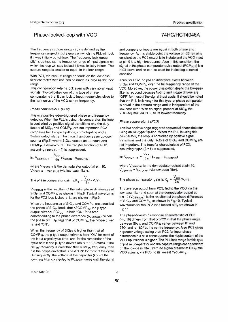
Philips Semiconductors
Phase-locked-loop with VCO
The frequency capture range (2fc) is defined as the frequency range of input signals on which the PLL will lock if it was initially out-of-lock. The frequency lock range (2fL) is defined as the frequency range of input signals on which the loop will stay locked if it was initially in lock. The capture range is smaller or equal to the lock range.
With PC1, the capture range depends on the low-pass filter characteristics and can be made as large as the lock range. This configuration retains lock even with very noisy input signals. Typical behaviour of this type of phase comparator is that it can lock to input frequencies close to the harmonics of the VCO centre frequency.
Phase comparator 2 (PC2)
This is a positive edge-triggered phase and frequency detector. When the PLL is using this comparator, the loop is controlled by positive signal transitions and the duty factors of SIG1N and COMP1N are not important. PC2 comprises two D-type flip-flops, control-gating and a 3-state output stage. The circuit functions as an up-down counter (Fig.S) where SIG1N causes an up-count and
COMP1N a down-count. The transfer function of PC2, assuming ripple (fr = fi) is suppressed,
. Vee IS: V DEMOUT = 41t ( <i>siGIN- <i>eOMPIN)
where VoEMOUT is the demodulator output at pin 1 0; VoEMOUT = Vpe2our (via low-pass filter).
v The phase comparator gain is: KP =
4c1tc (V / r) .
VoEMOUT is the resultant of the initial phase differences of SIG1N and COMP1N as shown in Fig.8. Typical waveforms for the PC21oop locked at f0 are shown in Fig.9.
When the frequencies of SIG1N and COMP1N are equal but the phase of SIG1N leads that of COMP1N. the p-type output driver at PC2our is held "ON" for a time corresponding to the phase difference (<l>oEMOuT). When the phase of SIG1N lags that of COMP1N, the n-type driver is held "ON".
When the frequency of SIG1N is higher than that of COMP1N. the p-type output driver is held "ON" for most of the input signal cycle time, and for the remainder of the cycle both n and p- type drivers are "OFF" (3-state). If the SIG1N frequency is lower than the COMP1N frequency, then it is the n-type driver that is held "ON" for most of the cycle. Subsequently, the voltage at the capacitor (C2) of the low-pass filter connected to PC2our varies until the signal
1997 Nov 25 3
80
Product specification
7 4HC/HCT 4046A
and comparator inputs are equal in both phase and frequency. At this stable point the voltage on C2 remains constant as the PC2 output is in 3-state and the VCO input at pin 9 is a high impedance. Also in this condition, the signal at the phase comparator pulse output (PC Pour) is a HIGH level and so can be used for indicating a locked condition.
Thus, for PC2, no phase difference exists between SIG1N and COMP1N over the full frequency range of the VCO. Moreover, the power dissipation due to the low-pass filter is reduced because both p and n-type drivers are "OFF" for most of the signal input cycle. It should be noted that the PLL lock range for this type of phase comparator is equal to the capture range and is independent of the low-pass filter. With no signal present at SIG 1N the VCO adjusts, via PC2, to its lowest frequency.
Phase comparator 3 (PC3)
This is a positive edge-triggered sequential phase detector using an RS-type flip-flop. When the PLL is using this comparator, the loop is controlled by positive signal transitions and the duty faotors of SIG1N and COMP1N are not important. The transfer characteristic of PC3, assuming ripple (fr = fi) is suppressed,
. Vee IS: V DEMOUT = 21t ( <i>siGIN- <i>eoMPIN)
where VoEMOUT is the demodulator output at pin 1 0; VoEMOUT = VpcJOUT (via low-pass filter).
v The phase comparator gain is: KP = 2~c (V /r).
The average output from PC3, fed to the VCO via the low-pass filter and seen at the demodulator output at pin 10 (VoEMOur). is the resultant of the phase differences of SIG1N and COMP1N as shown in Fig.1 0. Typical waveforms for the PC3 loop locked at f0 are shown in Fig.11.
The phase-to-output response characteristic of PC3 (Fig.10) differs from that of PC2 in that the phase angle between SIG1N and COMP1N varies between 0° and 360° and is 180° at the centre frequency. Also PC3 gives a greater voltage swing than PC2 for input phase differences but as a consequence the ripple content of the VCO input signal is higher. The PLL lock range for this type of phase comparator and the capture range are dependent on the low-pass filter. With no signal present at SIG1N the VCO adjusts, via PC3, to its lowest frequency.
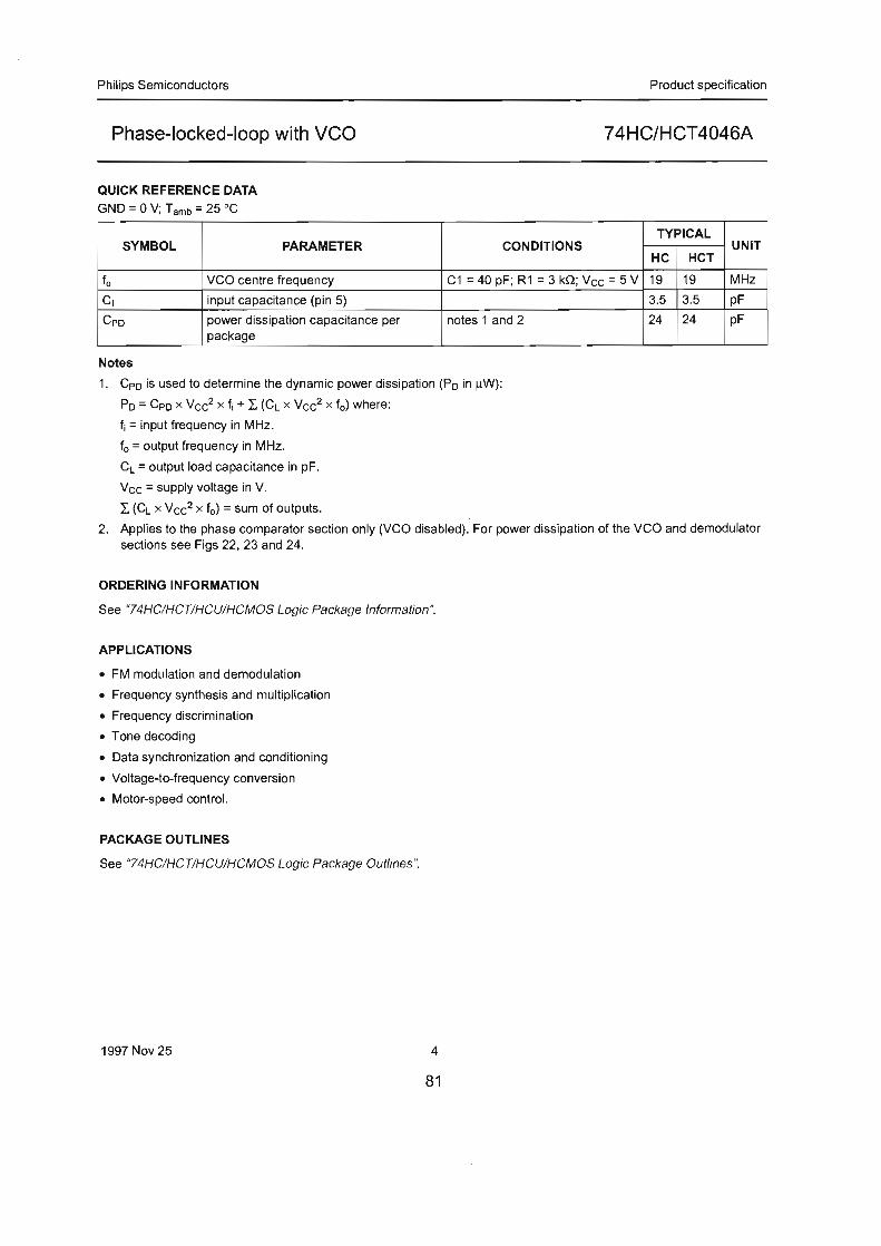
Philips Semiconductors
Phase-locked-loop with VCO
QUICK REFERENCE DATA
GND = 0 V; T amb = 25 oc
SYMBOL PARAMETER
fo VCO centre frequency
c1 input capacitance (pin 5)
Cpo power dissipation capacitance per package
Notes
Product specification
7 4HC/HCT 4046A
TYPICAL CONDITIONS UNIT
HC HCT
C1 = 40 pF; R1 = 3 kil; Vee= 5 V 19 19 MHz
3.5 3.5 pF
notes 1 and 2 24 24 pF
1. Cpo is used to determine the dynamic power dissipation (Po in f.tW):
Po= Cpo x Vee2 x f; + L. (CL x Vee2 x f0 ) where:
f; =input frequency in MHz.
f0 =output frequency in MHz.
CL =output load capacitance in pF.
Vee= supply voltage in V.
L. (CL x Vce2 x f0 ) =sum of outputs.
2. Applies to the phase comparator section only (VCO disabled). For power dissipation of the VCO and demodulator sections see Figs 22, 23 and 24.
ORDERING INFORMATION
See "74HC!HCT!HCU/HCMOS Logic Package Information".
APPLICATIONS
• FM modulation and demodulation
• Frequency synthesis and multiplication
• Frequency discrimination
• Tone decoding
• Data synchronization and conditioning
• Voltage-to-frequency conversion
• Motor-speed control.
PACKAGE OUTLINES
See '"74HC!HCT/HCU/HCMOS Logic Package Outlines".
1997 Nov 25 4
81
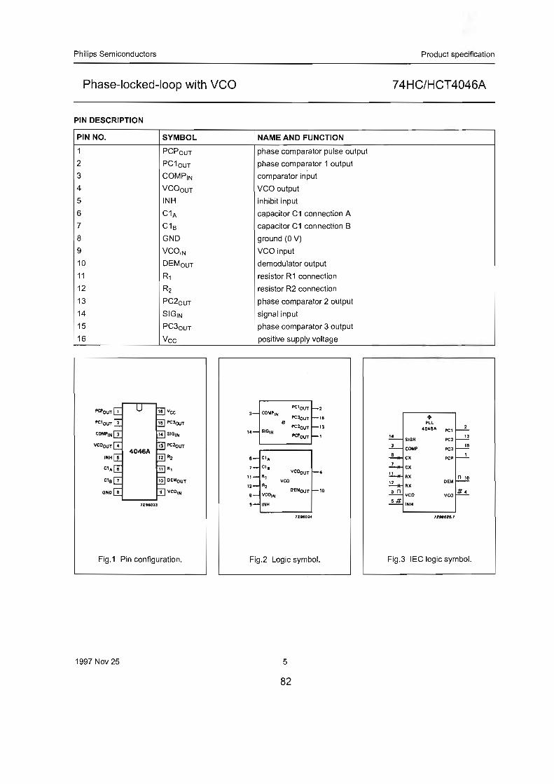
Philips Semiconductors
Phase-locked-loop with VCO
PIN DESCRIPTION
PIN NO. SYMBOL
1 PC PouT
2 PC1ouT
3 COM PIN
4 VCOouT
5 INH
6 C1A
7 C1s
8 GND
9 VCOIN
10 DEMouT
11 R1
12 R2
13 PC2ouT
14 SIGIN
15 PC3ouT
16 Vee
Fig.1 Pin configuration.
1997 Nov 25
NAME AND FUNCTION
phase comparator pulse output
phase comparator 1 output
comparator input
VCO output
inhibit input
capacitor C1 connection A
capacitor C1 connection B
ground (0 V)
VCO input
demodulator output
resistor R1 connection
resistor R2 connection
phase comparator 2 output
signal input
phase comparator 3 output
positive supply voltage
PC1ouT r--2 3- COMP1N
PCJoUT r--11 II
SIGIH PC :loUT r-u
14-PCI'oUT r'
e- C1A ,_ c1 8
VCOouT l-4 11-R1
vco 12- R2
DE "<JUT r-1o g- VCOIN
e- INH
7lU0241
Fig.2 Logic symbol.
5
82
Product specification
74HC/HCT4046A
14 SIGN
• PlL 4041A PCl
PC2
COMP PC3
IZWI<JII.I
Fig.3 IEC logic symbol.

Philips Semiconductors
Phase-locked-loop with VCO
C1
PC1ouT 2 ' '
' PC2ouT ' 13 ' ' ' R3 PCP ouT 1
..... ~ -'' - ' ' R4 '
PC3ouT 15 '
(a)
Fig.4 Functional diagram.
Cl
R2
R1
6 •
Fig.5 Logic diagram.
1997 Nov 25 6
83
idenlical to 4046A
I I I I I I
L
Product specification
7 4HC/HCT4046A
7046A
PC2ouT 13
LD 1
(b)
PC1our 2
I I I I I
PC3our I
15 I II II II II II II II II II II ~
' I 13 __ J
PCPour 1
TZHO.I.J

Philips Semiconductors Product specification
Phase-locked-loop with VCO 74HC/HCT4046A
7ZUQ27 lice
llo£MOU1" lAIII
1/211cc
v Voe~.tour = VPC2our = ~c ( ~SIGIN- ~CO lAPIN)
~DEIAOUT = (~SIGIN- ~OIAPIN) ·
Fig.6 Phase comparator 1: average output voltage versus input phase difference.
- 11cc
~GND 1Z112Jf
Fig.? Typical waveforms for PLL using phase comparator 1, loop locked at f0 .
lice 7Z'H02t
llo£MOUT lAIII
1/211cc
0~------r-----~ -38o" o• •380°
-"OEMOUT
v Voe~.tour = Vpc2our = 4c"c ( ~siGIN- ~COIAPIN)
~DEIAOUT = (~SIGIN - ~OIAPINJ ·
Fig.8 Phase comparator 2: average output voltage versus input phase difference.
1997 Nov 25 7
84

Philips Semiconductors
Phase-locked-loop with VCO
COMP 1N
VCOOUT
Pe2oUT
_fl___ ... JL ... _n_ _n_ .. -JL ... .IL J"'t·-·-·-·-·-·-·--·1 ("--Vee
~---twghimpedMceOFF·tute GNO
vco1N __,.,---·----·-.........____
I'CI'our u-··· ---~IIOJO
Product specification
74HC/HCT4046A
Fig.9 Typical waveforms for PLL using phase comparator 2, loop locked at f0 .
Vee VoeMour = Vpe3our = 2it (<llsoGoN- <lleoMPoNl
<ilOEMOUT = (<!>SIGIN - <ilcOMPIN).
VOEMOUT IAVI
1/:ZVcc
7ZIIGll
I I I I I I I i
0~----r---~ 0° 180° 380°
"oEMOUT
Fig.1 0 Phase comparator 3: average output voltage versus input phase difference:
1997 Nov 25
COMPJN veoOUT
PC louT
Fig.11 Typical waveforms for PLL using phase comparator 3, loop locked at f0 .
8
85

Philips Semiconductors Product specification
Phase-locked-loop with VCO 7 4H C/H CT 4046A
RECOMMENDED OPERATING CONDITIONS FOR 74HC/HCT
' 74HC 74HCT SYMBOL PARAMETER UNIT CONDITIONS
min. typ. max. min. typ. max.
Vee DC supply voltage 3.0 5.0 6.0 4.5 5.0 5.5 v Vee DC supply voltage if VCO 2.0 5.0 6.0 4.5 5.0 5.5 v
section is not used
v, DC input voltage range 0 Vee 0 Vee v Vo DC output voltage range 0 Vee 0 Vee v Tamb operating ambient -40 +85 -40 +85 oc see DC and AC
temperature range CHARACTERISTrCS
Tamb operating ambient -40 +125 -40 +125 oc temperature range
t,, It input rise and fall times (pin 5) 6.0 1000 6.0 500 ns Vee= 2.0V
6.0 500 6.0 500 ns Vcc =4.5V
6.0 400 6.0 500 ns Vee = 6.0 V
RATINGS
Limiting values in accordance with the Absolute Maximum System (IEC 134) Voltages are referenced to GND (ground = 0 V)
SYMBOL PARAMETER MIN. MAX. UNIT CONDITIONS
Vee DC supply voltage -0.5 +7 v ±I1K DC input diode current 20 mA for V1 < -0.5 V or V1 > Vee + 0.5 V
±loK DC output diode current 20 niA for V0 < -0.5 V or V0 > Vee + 0.5 V
±lo DC output source or sink 25 mA for - 0.5 V < V0 < Vee + 0.5 V current
±Icc; ±IGND DC Vee or GND current 50 mA
Tstg storage temperature range - 65 +150 oc Ptot power dissipation per package for temperature range: - 40 to +125 oc
74HC/HCT plastic OIL 750 mW above + 70 oc: derate linearly with 12 mW/K
plastic mini-pack (SO) 500 mW above + 70 oc: derate linearly with 8 mW/K
1997 Nov 25 9
86
I
Philips Semiconductors Product specification
Phase-locked-loop with VCO 74HC/HCT4046A
DC CHARACTERISTICS FOR 74HC
Quiescent supply current
Voltages are referenced to GND (ground = 0 V)
lamb (°C) TEST CONDITIONS
74HC Vee SYMBOL PARAMETER UNIT (V) OTHER
+25 -40 to +85 -40 to +125
min. typ. max. min. max. min. max.
quiescent supply pins 3, 5, and 14 at Vee:
Icc current (VCO 8.0 80.0 160.0 ~ 6.0 pin 9 at GND; 1'1 at pins disabled) 3 and 14 to be excluded
Phase comparator section
Voltages are referenced to GND (ground = 0 V)
lamb (°C) TEST CONDITIONS
SYM- 74HC Vee
BOL PARAMETER UNIT (V) OTHER
+25 -40 to +85 -40 to +125 v, min. typ. max. min. max. min. max. I
v,H DC coupled 1.5 1.2 1.5 1.5 v 2.0 I
HIGH level input voltage 3.15 2.4 3.15 3.15 4.5 SIGrN. COMPrN
4.2 3.2 4.2 4.2 6.0
v,L DC coupled 0.8 0.5 0.5 0.5 v 2.0 LOW level input voltage 2.1 1.35 1.35 1.35 4.5 SIGrN. COMPrN
2.8 1.8 1.8 1.8 6.0
VoH HIGH level output voltage 1.9 2.0 1.9 1.9 v 2.0 v,H -10 = 20 j.tA
PCPour. PCnour 4.4 4.5 4.4 4.4 4.5 or -10 = 20 j.tA
5.9 6.0 5.9 5.9 6.0 v,L
-10 = 20 j.tA
VoH HIGH level output voltage 3.98 4.32 3.84 3.7 v 4.5 v,H -lo = 4.0 rnA
PCPour. PCnour 5.48 5.81 5.34 5.2 6.0 or -lo = 5.2 rnA v,L
VoL LOW level output voltage 0 0.1 0.1 0.1 v 2.0 v,H 10 = 20 j.tA
PCPour. PCnour 0 0.1 0.1 0.1 4.5 or 10 = 20 j.tA
0 0.1 0.1 0.1 6.0 VrL 10 = 20 j.tA
VoL LOW level output voltage 0.15 0.26 0.33 0.4 v 4.5 I VrH 110 =4.0 rnA
PCPour. PCnour 0.16 0.26 0.33 0.4 6.0 I or 10 = 5.2 rnA VrL
±lr input leakage current 3.0 4.0 5.0 ~ 12.0 Vee SIGrN. COMPrN 7.0 9.0 11.0 3.0 or
18.0 23.0 27.0 4.5 GND
30.0 38.0 45.0 6.0
±loz 3-state 0.5 5.0 10.0 ~ 6.0 VrH Vo =Vee or OFF-state current or GND
PC2our v,L
1997 Nov 25 10
87

Philips Semiconductors Product specification
Phase-locked-loop with VCO 7 4HC/HCT 4046A
lamb (°C) TEST CONDITIONS
SYM- 74HC Vee
BOL PARAMETER UNIT (V) OTHER
+25 -40 to +85 -40 to +125 VI
min. typ. max. min. max. min. max.
R1 input resistance 800 kn 3.0 V1 at self-bias SIGIN• COMP1N 250 kn 4.5 operating point;
150 kn 6.0 1'1 V1 = 0.5 V; see Figs 12, 13 and 14
VCO section
Voltages are referenced to GND (ground = 0 V)
lamb (°C) TEST CONDITIONS
SYM- 74HC Vee
BOL PARAMETER UNIT (V) OTHER
+25 -40to +85 -40 to +125 VI
min. typ. max. min. max. min. max.
V1H HIGH level 2.1 1.7 2.1 2.1 v 3.0 input voltage 3.15 2.4 3.15 3.15 4.5 INH
4.2 3.2 4.2 4.2 6.0
VIL LOW level 1.3 0.9 0.9 0.9 v 3.0 input voltage 2.1 1.35 1.35 1.35 4.5 INH
2.8 1.8 1.8 1.8 6.0
VoH HIGH level 2.9 3.0 2.9 2.9 v 3.0 VIH -lo = 20 IJ.A output voltage 4.4 4.5 4.4 4.4 4.5 or -10 = 20 IJ.A VCOour
5.9 6.0 5.9 5.9 6.0 VIL -10 = 20 1J.A VoH HIGH level 3.98 4.32 3.84 3.7 v 4.5 VIH -lo = 4.0 mA
output voltage 5.48 5.81 5.34 5.2 6.0 or -lo = 5.2 mA VCOour V1L
VoL LOW level 0 0.1 0.1 0.1 v 3.0 V1H j
1
1o = 20 IJ.A output voltage 0 0.1 0.1 0.1 4.5 or 10 = 20 1J.A VCOour 0 0.1 0.1 0.1 6.0 V1L l lo = 20 IJ.A
VoL LOW level 0.15 0.26 0.33 0.4 v 4.5 VIH lo = 4.0 mA output voltage 0.16 0.26 0.33 0.4 6.0 or lo = 5.2 mA VCOour VIL
VoL LOW level output 0.40 0.47 0.54 v 4.5 VIH lo =4.0 mA voltage C1A, C1s 0.40 0.47 0.54 6.0 or
VIL 10 = 5.2 mA
±II input leakage 0.1 1.0 1.0 IJ.A 6.0 Vee current or
INH, VC01N GND
R1 resistor range 3.0 300 kn 3.0 note 1
3.0 300 4.5
3.0 300 6.0
1997 Nov 25 11
88

Philips Semiconductors Product specification
Phase-locked-loop with VCO 7 4 H C/HCT 4046A
Tamb (°C) TEST CONDITIONS
SYM- 74HC Vee
BOL PARAMETER UNIT (V) OTHER
+25 -40 to +85 -40 to +125 VI
min. typ. max. min. max. min. max.
R2 resistor range 3.0 300 kn 3.0 note 1
3.0 300 4.5
3.0 300 6.0
C1 capacitor range 40 no pF 3.0
40 limit 4.5
40 6.0
VvcOIN operating voltage 1.1 1.9 v 3.0 over the range range at VC01N 1.1 3.4 4.5 specified for
1.1 4.9 6.0 R1; for linearity see Figs 20 and 21
Note
1. The parallel value of R1 and R2 should be more than 2.7 kn. Optimum performance is achieved when R1 and/ or R2 are/is > 1 0 kn.
Demodulator section
Voltages are referenced to GND (ground = 0 V)
Tamb (°C) TEST CONDITIONS
74HC SYMBOL PARAMETER UNIT Vee OTHER
+25 -40to+85 -40 to +125 v min. typ. max. min. max. min. max.
Rs resistor range 50 300 kn 3.0 at Rs > 300 kn
50 300 4.5 the leakage current can
50 300 6.0 influence VoEMOUT
VoFF offset voltage ±30 mV 3.0 V1 = VvcoiN = 1/2 Vee; VC01N to VoEMOUT ±20 4.5 values taken over
±10 6.0 Rs range; see Fig.15
Ro dynamic output 25 n 3.0 VoEMOUT = 1/2 Vee resistance at DEMour 25 4.5
25 6.0
1997 Nov 25 12
89

Philips Semiconductors Product specification
Phase~locked~loop with VCO 7 4HC/HCT 4046A
AC CHARACTERISTICS FOR 74HC
Phase comparator section
GND = 0 V; tr = tr = 6 ns; CL = 50 pF
Tamb (0 C) TEST
CONDITIONS
SYMBOL PARAMETER 74HC UNIT OTHER
+25 -40to +85 -40 to +125 Vee (V)
min. typ. max. min. max. min. max.
tPHL/ propagation delay 63 200 250 300 ns 2.0 I Fig.16 tPLH SIGINo CQMPIN 23 40 50 60 4.5
to PC1our 18 34 43 51 6.0
tpHL/ propagation delay 96 340 425 510 ns 2.0 Fig.16
tPLH SIG1N. COMP1N 35 68 85 102 4.5 to PCPour
28 58 72 87 16.0
tPHL/ propagation delay 77 270 340 405 I ns 2.0 Fig.16
tPLH SIGIN· COMPIN 28 54 68 81 4.5 to PC3our
22 46 58 69 6.0
tpzw 3-state output enable 83 280 350 420 ns 2.0 ( ig.17 tpzL time SIG1N• COMP1N 30 56 70 84 4.5
to PC2our 24 48 60 71 6.0
tpHz/ 3-state output disable 99 325 405 490 ns 2.0 Fig.17
tpLZ time SIGIN• COMP1N 36 65 81 98 4.5 to PC2our
29 55 69 83 6.0
trHL/ output transition time 19 75 95 110 ns 2.0 Fig.16
tTLH 7 15 19 22 4.5
6 13 16 19 6.0
vi(P·P> AC coupled input sensitivity 9 mV 2.0 fi = 1 MHz (peak-to-peak value) at 11 3.0 SIG1N or COMP1N
15 4.5
33 6.0
1997 Nov 25 13
90

Philips Semiconductors Product specification
Phase-locked-loop with VCO 7 4HC/HCT 4046A
VCO section
GND = 0 V; t, = tt = 6 ns; CL = 50 pF
Tamb (°C) TEST CONDITIONS
74HC SYMBOL PARAMETER UNIT Vee OTHER
+25 -40 to +85 -40 to +125 (V)
min. typ. max. typ. max. min. max.
MfT frequency stability 0.20 %/K 3.0 v, = VvcoiN = 1/2 Vee; with temperature 0.15 4.5 R1 = 100 kQ; R2 = oo; change
0.14 6.0 C1 = 100 pF; see Fig.18
fo VCO centre 7.0 10.0 MHz 3.0 VvcoiN = 1/2 Vee; frequency (duty 11.0 17.0 4.5 R 1 = 3 kQ; R2 = oo; factor= 50%)
13.0 21.0 6.0 C1 = 40 pF; see Fig.19
Mvco VCO frequency 1.0 % 3.0 R1 = 100 kQ; R2 = oo; linearity 0.4 4.5 C1 = 100 pF;
0.3 6.0 see Figs 20 and 21
Ovco duty factor at 50 % 3.0 VCOour 50 4.5
50 6.0
DC CHARACTERISTICS FOR 74HCT
Quiescent supply current
Voltages are referenced to GND (ground = 0 V)
Tamb (°C) TEST CONDITIONS
74HCT SYMBOL PARAMETER UNIT Vee OTHER
+25 -40 to +85 -40 to +125 (V)
min. typ. max. min. max. min. max.
Icc quiescent supply 8.0 80.0 160.0 j.iA 6.0 pins 3, 5 and 14 current at Vee; pin 9 at (VCO disabled) GND; 11at
pins 3 and 14 to be excluded
6.1cc additional quiescent 100 360 450 490 j.iA 4.5 pins 3 and 14 supply current per to at Vee; input pin for unit load 5.5 pin 9 at GND; coefficient is 1 (note 1) 11 at pins 3 and 14 V,=Vcc- 2.1 V to be excluded
Note
1. The value of additional quiescent supply current (6-lcc) for a unit load of 1 is given above. To determine 6-lcc per input, multiply this value by the unit load coefficient shown in the table below.
I INPUT INH
I UNIT LOAD COEFFICIENT
1.00
1997 Nov 25 14
91

Philips Semiconductors Product specification
Phase-locked-loop with VCO 7 4HC/HCT 4046A
DC CHARACTERISTICS FOR 74HCT
Phase comparator section
Voltages are referenced to GND (ground = 0 V)
lamb (°C) TEST CONDITIONS
74HCT SYMBOL PARAMETER UNIT Vee v, OTHER
+25 -40 to +85 -40 to +125 (V)
min typ. max min max min. max.
v,H DC coupled 3.15 2.4 v 4.5 HIGH level input
voltage SIG1N. COMP1N
v,L DC coupled 2.1 1.35 v 4.5 LOW level input
voltage SIG,N. COMP1N
VoH HIGH level output 4.4 4.5 4.4 4.4 v 4.5 v,H -10 = 20 j.lA voltage PCPouT. or PCnoUT v,L
VoH HIGH level output 3.98 4.32 3.84 3.7 v 4.5 v,H -lo = 4.0 mA voltage PCPouT. or PCnoUT v,L
Vm LOW level output 0 0.1 0.1 0.1 v 4.5 v,H lo = 20 j.lA voltage or
PCPouT. PCnoUT v ,L
VoL LOW level output 0.15 0.26 0.33 0.4 v 4.5 v,H lo =4.0 mA voltage or
PCPouT. PCnoUT v,L
±1, input leakage current 30 38 45 ~ 5.5 Vee SIG,N. COMP1N or
GN D
±loz 3-state OFF-state 0.5 5.0 10.0 ~ 5.5 v,H Vo =Vee or current PC2ouT or GND
v,L
R, input resistance 250 kn 4.5 V1 at self-bias SIGIN· COMPin operating
point; 1J. V, = 0.5 V; see Figs 12, 13 and 14
1997 Nov 25 15
92

Philips Semiconductors Product specification
Phase-locked-loop with VCO 7 4HC/HCT 4046A
DC CHARACTERISTICS FOR 74HCT
VCO section
Voltages are referenced to GND (ground = 0 V)
Tamb (°C) TEST CONDITIONS
74HCT SYMBOL PARAMETER UNIT Vee VI OTHER
+25 -40 to +85 -40 to +125 (V)
min typ. max min max min. max.
VIH HIGH level 2.0 1.6 2.0 2.0 v 4.5 input voltage INH to
5.5
VIL LOW level 1.2 0.8 0.8 0.8 v 4.5 input voltage INH to
5.5
VoH HIGH level output 4.4 4.5 4.4 4.4 v 4.5 VIH -lo = 20~ voltage VCOouT or
VIL
VoH HIGH level output 3.98 4.32 3.84 3.7 v 4.5 VIH -lo = 4.0 mA voltage VCOouT or
VIL
VoL LOW level output 0 0.1 0.1 0.1 v 4.5 VIH lo = 20 ~ voltage VCOouT or
VIL
VoL LOW level output 0.15 0.26 0.33 0.4 v 4.5 VIH lo = 4.0 mA voltage VCOouT or
V1L
VOL LOW level output 0.40 0.47 0.54 v 4.5 VIH lo =4.0 mA voltage C1A. C1 8 or (test purposes only) V1L
±l1 input leakage 0.1 1.0 1.0 ~ 5.5 Vee current or
INH, VCOIN GND
R1 resistor range 3.0 300 kn 4.5 note 1
R2 resistor range 3.0 300 kn 4.5 note 1
C1 capacitor range 40 no pF 4.5 limit
VveoiN operating voltage 1.1 3.4 v 4.5 over the range at VC01N range
specified for R1; for linearity see Figs 20 and 21
Note
1. The parallel value of R1 and R2 should be more than 2.7 kn. Optimum performance is achieved when R1 and/or R2 are/is> 10 kn.
1997 Nov 25 16
93

Philips Semiconductors Product specification
Phase-locked-loop with VCO 7 4HC/HCT 4046A
DC CHARACTERISTICS FOR 74HCT
Demodulator section
Voltages are referenced to GND (ground = 0 V)
lamb (oC) TEST CONDITIONS
74HCT SYMBOL PARAMETER UNIT Vee OTH'ER
+25 -40 to +85 -40 to +125 (V)
min. typ. max. min. max. min. max.
Rs resistor range 50 300 kn 4.5 at Rs > 300 kn I the leakage current can influence VoeMour
VoFF offset voltage ±20 mV 4.5 V, = VvcOIN = 1/2 Vee; vco1N to I values taken over VoeMour ! Rs range; see Fig.15
Ro dynamic output 25 n 4.5 VoeMour = 1/2 Vee resistance at
I DEMour
AC CHARACTERISTICS FOR 74HCT
Phase comparator section
GND = 0 V; t, = t1 = 6 ns; CL =50 pF
lamb (°C) TEST CONDITIONS
74HCT SYMBOL PARAMETER UNIT Vee OTHER
+25 -40 to +85 -40 to +125 (V)
min. typ. max. min. max. min. max.
IPHL/ propagation delay 23 40 50 60 ns il 4.5 Fig.16
IPLH SIGIN· COMPIN I
to PC1our i
IPHL/ propagation delay 35 68 85 102 ns 4.5 Fig.16 IPLH SIGIN· COMP1N
to PCPour
IPHL/ propagation delay 28 54 68 81 ns 4.5 Fig.16
IPLH SIG,N, COMP1N I
to PC3our
lpzHf 3-state output enable 30 56 70 84 ns 4.5 Fig.17
lpzL time SIG1N, COMP1N to PC2our
1997 Nov 25 17
94
Philips Semiconductors Product specification
Phase-locked-loop with VCO 74HC/HCT4046A
lamb (°C) TEST CONDITIONS
74HCT SYMBOL PARAMETER UNIT Vee OTHER
+25 -40 to +85 -40 to +125 (V)
min. typ. max. min. max. min. max.
tpHz/ 3-state output disable 36 65 81 98 ns 4.5 Fig.17 !pLZ time SIGIN· COMPIN
to PC2ouT
ITHL/ output transition time 7 15 19 22 ns 4.5 Fig.16 ITLH
VI (p-p) AC coupled input 15 mV 4.5 fi = 1 MHz sensitivity
(peak-to-peak value) at
SIG1N or COMP1N
VCO section
GND = 0 V; t, = It= 6 ns; CL = 50 pF
lamb (°C) TEST CONDITIONS
74HCT SYMBOL PARAMETER UNIT Vee OTHER
+25 -40 to +85 -40 to +125 (V)
min. typ. max min. max min. max.
MIT frequency stability 0.15 %/K 4.5 V1 = VvcOIN withi with temperature n recommended change range;
R1 = 100 kn; R2 = oo; C1 = 100 pF; see Fig.18b
fo VCO centre frequency 11.0 17.0 MHz 4.5 VvcoiN = 1/2 Vee (duty factor= 50%) '
R1 = 3 kn ; R2 = oo; C1 = 40 pF; see Fig.19
Mvco VCO frequency 0.4 % 4.5 R1 = 100 kn; linearity R2 = oo;
C1 = 100 pF; see Figs 20 and 21
Ovco duty factor at VCOouT 50 % 4.5
1997 Nov 25 18
95

Philips Semiconductors
Phase-locked-loop with VCO
FIGURE REFERENCES FOR DC CHARACTERISTICS
lZMOll
'•
...... ~.ct"' point
/ v,
Fig.12 Typical input resistance curve at SIGIN· COMPIN·
+I
'• I ,.AI
1 0V
4.~v
t;;; -I
1/2Vcc-0.25
" v v v
1ZH0ll1
Vee •II.OV v I-' X ~ 1-"
It 10V
r
Fig.14 Input current at SIG1N. COMP1N with t:J.V1 = 0.5 Vat self-bias point.
1997 Nov 25 19
96
BOO
Ro (kSll
800
400
200
"
r---. r-... I-1--
0 112Vcc-o.25
\
"
Product specification
74HC/HCT4046A
l'ZH034 1
Vcc•10V /
I I
\ I \ v 4.5 V ,.....
',, I Vi: r-...... -..\.. V- 1--'~ov
"':" ~
Fig.13 Input resistance at SIG1N. COMP1N with t:J.V1 = 0.5 Vat self-bias point.
+80
VoFF lmV I
+40
+20
-20
-R5 =50 kn - - - - Rs = 300 kn
r-
7ZU031 I
I If /.
vcc•J.ov I I 1/.1 ~ h
,. 1,
1av ./. / -~ ;"
II.OV ./.,"/
r 112 Vcc
VvcorN tVJ
Fig_15 Offset voltage at demodulator output as a function of VC01N and Rs.

Philips Semiconductors Product specification
Phase-locked-loop with VCO 7 4HC/HCT 4046A
AC WAVEFORMS
\_ _j 7ZII037 ..J - 1TLH
Fig.16 Waveforms showing input (SIG1N. COMP1N) to output (PCPour. PC1our. PC3our) propagation delays and the output transition times.
SIGIN INPUT
COMPIN INPUT
PC2our OUTPUT
(1) HC : V,. =50%; V1 = GND to Vee
7ZNOJS
Fig.17 Waveforms showing the 3-state enable and disable times for PC2our.
1997 Nov 25 20
97
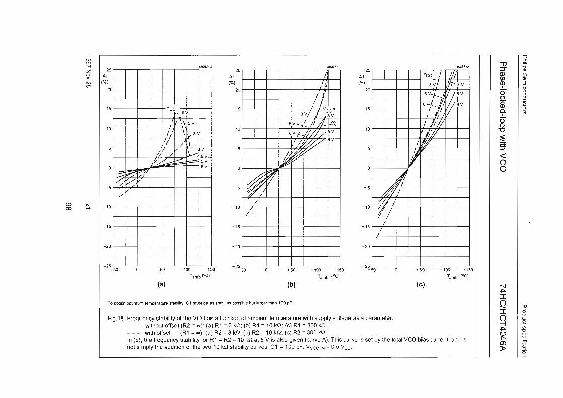
co co --.J
z 0 < 1\.) 0'1
<.0 1\.)
co -->.
I 25
(~) 20
r-15
10
5
I; 7'/.
0
-5
~ ""'L__ d ~ v / L
...... v -10
-15
-20
-25
MSB710
v = CC 6V ~_J
j_ lj _1\-sv
II \ / 3 v
1.' I /' \ L-/ ~sv_
..,;:; f-:::::: ~5V 6V_
25
Ll.f (%)
20
15
10
5
0
-5
-10
-15
-20
-25
"---
ij ~ ~ !011 ~ ~/ h
1/ ;'
I
/ 3VI
sv----, f-... ;I 6V-f-J~ II/~ ~ /~ v
~ v
MS8711
I / fl
II j' I. If vee=-
3V
lfft® V /~v vsv-
25
Ll.f (%)
20
15
10
5
0
-5
-10
-15
-20
-25
MS8712
vee= I .0 3 vl ~t.t-:3 v
5V Y--.!J (/I 5V
SV..J. r--1.1 1/;sv
/ Ill'; v I i II/ iil v
lk'#' jJ_
"--.J A WI
bfJ I ~ VI 'I I
/ !
-50 0 50 100 150 -so 0 +50 + 100 +150 -50 0 +50 +100 +150
lamb (oC) lamb (0 C)
(a) (b)
To obtain optimum temperature stability, C1 must be as small as possible but larger than 100 pF.
Fig.18 Frequency stability of the VCO as a function of ambient temperature with supply voltage as a parameter. -- without offset (R2 = oo): (a) R1 = 3 kn; (b) R1 = 10 kil; (c) R1 = 300 kil. --- with offset (R1 = oo): (a) R2 = 3 kil; (b) R2 = 10 kil; (c) R2 = 300 kn.
lamb (oC)
(c)
In (b), the frequency stability for R1 = R2 = 10 kil at 5 Vis also given (curve A). This curve is set by the total VCO bias current, and is not simply the addition of the two 10 kn stability curves. C1 = 100 pF; Vvco tN = 0.5 Vee-
"U :::J"' Ill C/)
CD I
0 (') 7\ CD 0.
I
0 0 "'0
~-....... :::J"'
< () 0
........ ~ I () -I ()
~ 0 ~ Q) )>
-u ::::T
"0 CJ>
UJ m 3 a· 0 :::J 0.. c
6 Cil
-u a 0.. c Sl. CJ> "0 m ()
~ g o· :::J
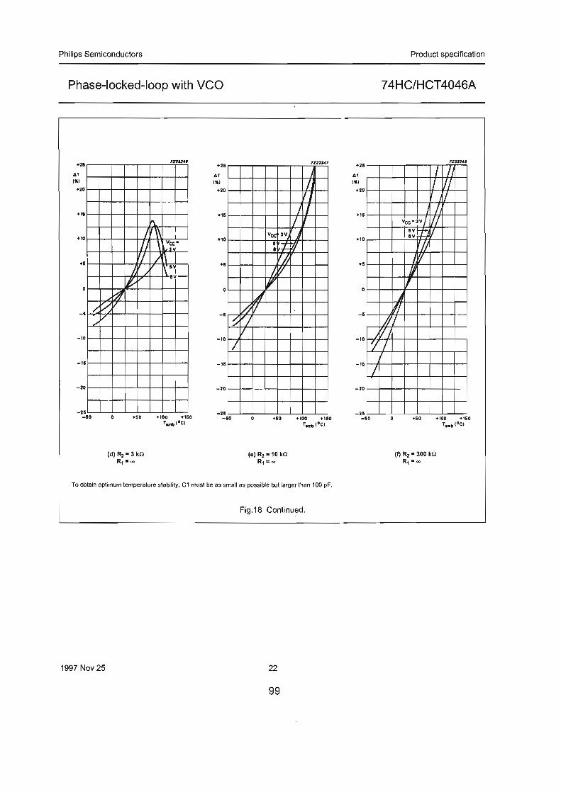
Philips Semiconductors
Phase-locked-loop with VCO
+21
4f
tlll
+20
+11
+10
I . --::
./
-10
_, I
-:to
-2 5 -50
I II ~I
h /
~ 11
~/ v
+60
~
" ' Vee• '311
L Ill
I 111-
+25
41 Ill I
+20
+II
+10
••
-· -10
-II
-20
-21
~
_f_
-50
I ,, Ill
1/ 'I voc 311 J : ;t: w
'!J h ~ ,
'A 'A '/ /
'I
+50 +100 +110 T....,t•ct
To obtain optimum temperature stability, C1 must be as small as possible but larger than 100 pF.
Fig.18 Continued.
1997 Nov 25 22
99
+2a
41
Ill I
+20
+II
+10
••
-· -10
-II
-20
-21
'L
I
-10
Product specification
7 4HC/HCT 4046A
I 1/ 1/
/, Vcc•3v / Ill =~~v
'II Iff
/J I
A IL
Jl 'IJ j
+60
(f) R2 • 300 kQ R1 • oo
/j VI [J_
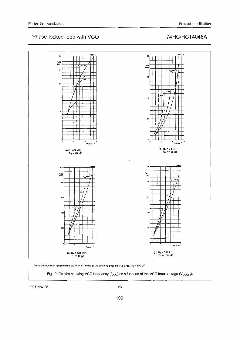
Philips Semiconductors
Phase-locked-loop with VCO
so JlMotJ
'vco \MHl)
Yoc•8.0V .. y
A UY
20
II 1-t-t--tf-t-t-t-+-i-+-t-H
10V
10 H-1-~H+t--1-++H
...
0
.
(a) R1 "3 kQ; C, •40 pF
• • Vy(lOI,_ IYI
Y«, •I.O~~
..~/ 1 /
1//
10V tV
II. v
'V I
. V lfWIN IV)
(c) R1 = 300 kQ; C1 "'40 pF
10
'vco lkHII
eo
20
0 0
'•oo \ HI I
-
, ..
D .
To obtain optimum temperature stability, C1 must be as small as possible but larger than 100 pF.
Product specification
7 4H C/H CT 4046A
Yoc•I.OY
1 I
<tV
10V 1/
I I
1/ I
/I IV v
VY II.~
li
• • VYCOIN IYl
(b) R, = 3 kQ; C1 = 100 nF
Voc•U v_j_
... $V 1/
I
3.ov !J r;
;,
/// w
. . VVCOIN l VI
(d) R1 " 300 kQ; C1 • 100 nF
Fig. 19 Graphs showing VCO frequency (fvco) as a function of the VCO input voltage (Vvco1N).
1997 Nov 25 23
100

Philips Semiconductors
Phase-locked-loop with VCO
t,
'z 'o 'ri
'1
7ZII048
min t/2Vcc
- VVCOIN
Fig.20 Definition of VCO frequency linearity: /'J.V = 0.5 V over the Vee range: for VCO linearity
+10
Alvco
"''
+5
-·
vee• I l.OV
uv I
e.ov
Vcc•4.5V
""7.100pF
e.o;-
,',~
l .,
10"1
1 1
Product specification
7 4H C/HCT 4046A
JUIIM7
!
I
'I be' • •••
1: I
I 1\
I
'\ I ~
. ..c I I I
~v !
V" l'e1 • 40pF I
I' II
10
f' -f linearity= T x 100%
0
Fig.21 Frequency linearity as a function of R1, C1 and Vee: R2 = oo and /'J.V = 0.5 V.
['.,
104 ~
'-t'
10
-e1 =40pF
•• • -e1 = 111F
7ZHO<I8
1'-o... Vee• e.ov •UV
10V
II II IIIII
Fig.22 Power dissipation versus the value of R 1: CL =50 pF; R2 = oo; VveoiN = 1/2 Vee: lamb= 25 °C.
1997 Nov 25
- e1 =40pF
-- -- e1 = 111F
Fig.23 Power dissipation versus the value of R2: CL =50 pF; R1 = oo; VveOIN = GND = 0 V; lamb= 25 °C.
24
101
10 10
!"-.
" "
7UIOIO
cc• e.ov
~·~ ~0~ "I
Fig.24 Typical de power dissipation of demodulator sections as a function of Rs: R1 = R2 = oo; lamb= 25 oc ; VveoiN = 1/2 Vee.
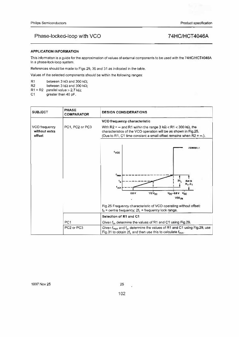
Philips Semiconductors Product specification
Phase-locked-loop with VCO 74HC/HCT4046A
APPLICATION INFORMATION
This information is a guide for the approximation of values of external components to be used with the 7 4HC/HCT4046A in a phase-lock-loop system.
References should be made to Figs 29, 30 and 31 as indicated in the table.
Values of the selected components should be within the following ranges:
R1 R2 R1 + R2 C1
between 3 k.n and 300 k.n; between 3 k.n and 300 k.n; parallel value> 2.7 k.n; greater than 40 pF.
SUBJECT PHASE COMPARATOR
VCO frequency PC1, PC2 or PC3 without extra offset
PC1
PC2 or PC3
1997 Nov 25
DESIGN CONSIDERATIONS
VCO frequency characteristic
With R2 = oo and R1 within the range 3 k.Q < R1 < 300 k.n, the characteristics of the VCO operation will be as shown in Fig.25. (Due to R1, C1 time constant a small offset remains when R2 = oo.).
- 1ZI.f1fl.l
'vco
I
,..,.. ------------------~!
t t fo 21L ~ItO
l R1,c 1 'min
---. L ' o.av 112vcc Vcc-0.9V vee VCOIN
Fig.25 Frequency characteristic of VCO operating without offset: fa = centre frequency; 2fL = frequency lock range.
Selection of R1 and C1
Given f0 , determine the values of R1 and C1 using Fig.29.
Given fmax and f0 , determine the values of R1 and C1 using Fig.29, use Fig.31 to obtain 2fL and then use this to calculate fmin·
25
102

Philips Semiconductors Product specification
Phase-locked-loop with VCO 74HC/HCT4046A
SUBJECT PHASE
DESIGN CONSIDERATIONS COMPARATOR
VCO frequency characteristic
VCO frequency PC1, PC2 or PC3 With R1 and R2 within the ranges 3 kn < R1 < 300 kn, with extra 3 kn < R2 < 300 kn, the characteristics of the VCO operation will be as offset shown in Fig.26.
1vco
-------------- r--TZHOI:LI
'max
----~-~ t ~!IC Ia 21L
1mln __ I I t R1.c1
1aff ~
I : I t I I I I I d ... to I I I R2.c1 I I I
: I I 1 I I
O.IIV 112vcc vcc-o.ev vee vco 1N
Fig.26 Frequency characteristic of VCO operating with offset: f0 =centre frequency; 2fL =frequency lock range.
Selection of R1, R2 and C1
PC1, PC2 or PC3 Given f0 and fL. determine the value of product R1 C1 by using Fig.31. Calculate foff from the equation foff = f0 - 1.6fL. Obtain the values of C1 and R2 by using Fig.30. Calculate the value of R1 from the value of C1 and the product R1 C1.
PLL conditions PC1 VCO adjusts to f0 with 4>oEMOUT = 90° and VveorN = 1/2 Vee (see Fig.6). with no signal at PC2 VCO adjusts to f0 with 4>oEMOUT = -360° and VveorN = min. (see Fig.8). the SIGrN input
PC3 VCO adjusts to f0 with 4>DEMOUT = -360° and Vveo1N =min. (see Fig.10).
1997 Nov 25 26
103

Philips Semiconductors
Phase-locked-loop with VCO
SUBJECT
PLL frequency capture range
PLL locks on harmonics at centre frequency
noise rejection at signal input
AC ripple content when PLL is locked
1997 Nov 25
PHASE COMPARATOR
PC1, PC2 or PC3
PC1 or PC3
PC2
PC1
PC2 or PC3
PC1
PC2
PC3
Product specification
7 4H C/H CT 4046A
DESIGN CONSIDERATIONS
Loop filter component selection
(a) 1: = R3 x C2 (b) amplitude characteristic (c) pole-zero diagram
A small capture range (2fc) is obtained if 2fc"' ~ J2nfLI't 1t
Fig . 27 Simple loop filter for PLL without offset; R3 ~ 500 n.
,,~,~~~ .. Ut_m• RHR4
1lr3 1/n w 7211014
(a) t1 = R3 x C2; (b) amplitude characteristic (c) pole-zero diagram t2 = R4 x C2; t3 = (R3 + R4) x C2
Fig.28 Simple loop filter for PLL with offset; R3 + R4 ~ 500 n. yes
no
high
low
fr = 2fi, large ripple content at <!>oEMOUT = goo
fr = fi, small ripple content at <!>oEMOUT = oa
fr = fi, large ripple content at <!>oEMOUT = 180o
27
104

Philips Semiconductors
Phase-locked-loop with VCO
'• (Hz)
104
10
I I
I
I
1
lA I• lkn ·
I• kn
1
{ I
~
~
" 1•150
kn:{ K ' 1•301
~
10 102
I ,, '
~~. ~
~
~ '\ ~~
~ r-...~
~ ~ """ ~~
&.
~ ~
' 10 10
To obtain optimum veo performance, e1 must be as small as possible but larger than 100 pF.
Product specification
7 4HC/HCT4046A
>:l :!_
'
I
I
' I
'
~
• ' ~ ' I r-....~ 'vee'
"~~ :I
4.5V
B=av I
' 1&. 3V
~~
::.v
~! ~~·ev
' 101
C1 (pfl 10 101
Interpolation for various values of R1 can be easily calculated because a constant R1e1 product will produce almost the same veo output frequency.
Fig.29 Typical value of VCO centre frequency (f0 ) as a function of C1: R2 = oo; VveoiN = 1/2 Vee: INH = GND; Tamb = 25 ac.
1997 Nov 25 28
105

Philips Semiconductors
Phase-locked-loop with VCO
'all {HI)
10 1
rR2·_ ... 1•10~
i2 •USOk
1•300kn
10
~
~
' ~
I"" i\
~~
~~
102
"" ~~ l': "X j\ ['\
~~
~ ~r.:: " ~
~ ~
"" ~~
'
I
1()3 10'
To obtain optimum VCO performance. C1 must be as small as possible but larger than 100 pF.
Product specification
74HC/HCT4046A
1ZHDI1,
.--.. I
"X I
'\t-, I '
~~-;
"' ~ 4.51
~
1\1 ·:~ =~e'
~ ~
I\ ~ : :.~": . !~.~
101 C1 fpf) 10° 107
Interpolation for various values of R2 can be easily calculated because a constant R2e1 product will produce almost the same veo output frequency.
Fig.30 Typical value of frequency offset as a function of C1: R1 = oo; VveOIN = 1/2 Vee; INH = GND; lamb= 25 oc.
1997 Nov 25 29
106

Philips Semiconductors
Phase-locked-loop with VCO
to•
to t
... :::::::::
o·'
~
I
I
' I
I
!
I
~
" '
I
to·• to· •
I I'
" ~ "
~
"" "
I 1\..
'
tO_. to·3
Product specification
7 4HC/HCT 4046A
1ZJION.r
,, '
' I I,
I
I
I
'
I
I II
~
~ I
I
' ~ I" I
' I
r"\ I
,"\. :;cv~ ~:r
I '\ ;·:1 to·2 RIC! !O"' ,
Fig.31 Typical frequency lock range (2fL) versus the product R1 C1: Vveo1N range= 0.9 to (Vee- 0.9) V; R2 = oo; VCO gain:
2fl . Kv = V 2n: ( r/ s/ V).
VeOIN range
1997 Nov 25 30
107
Philips Semiconductors
Phase-locked-loop with VCO
PLL design example
The frequency synthesizer, used in the design example shown in Fig.32, has the following parameters:
Output frequency: 2 MHz to 3 MHz frequency steps : 100 kHz settling time 1 ms overshoot < 20%
The open-loop gain is H (s) X G (s) = Kp x Kt x K0 x Kn.
Where:
Kp = phase comparator gain Kt = low-pass filter transfer gain K0 = Kv/s VCO gain Kn = 1/n divider ratio
The programmable counter ratio Kn can be found as follows:
fout 2 MHz Nmin. = f- = 100kHz = 20
step
N fout 3 MHz
max. = -f - = 100 kH = 30 step Z
The VCO is set by the values of R 1, R2 and C1, R2 = 10 kn (adjustable). The values can be determined using the information in the section "DESIGN CONSIDERATIONS". With f0 = 2.5 MHz and fL = 500 kHz this gives the following values (Vee= 5.0 V): R1=10kn R2=10kn C1 = 500 pF
1997 Nov 25
The VCO gain is:
2flx2x1t K = =---';:;-;--""""'-.-v 0.9 - (Vcc-0.9)
1 MHz 6 = --x2Jt = 2 x 10 r/sN 3.2 .
The gain of the phase comparator is:
Vee KP = 4 x 1t = 0.4 V/r.
The transfer gain of the filter is given by:
Where:
-r1 = R3C2 and -r2 = R4C2.
The characteristics equation is: 1 + H (s) x G (s) = 0.
This results in:
2 1 + Kp X Kv X Kn X 1:2 s + s+ (1:1 + 1:2)
Kp X Kv X Kn = O. (1:1 + 1:2)
The natural frequency Wn is defined as follows:
(() = n KP x Kv x Kn
(1:1 + 1:2) .
31
108
Product specification
7 4H C/H CT 4046A
and the damping value ~ is defined as follows:
In Fig.33 the output frequency response to a step of input frequency is shown.
The overshoot and settling time percentages are now used to determine wn. From Fig.33 it can be seen that the
damping ratio ~ = 0.45 will produce an overshoot of less than 20% and settle to within 5% at wnt = 5. The required settling time is 1 ms. This results in:
w = ~ = -5 - = 5 x 10
3 r/s
n t 0.001 ·
Rewriting the equation for natural frequency results in:
_ Kp X Kv X Kn (1:1+1:2) - 2
(J)n
The maximum overshoot occurs at Nmax·:
6 (1:1+1:2) = 0.4 x ~ x 10 = 0.0011 s.
5000 X 30
When C2 = 470 nF, then
(-r1 + -r2 ) x2xwn x ~-1 R4= =3150
Kp X Kv X Kn X C2
now R3 can be calculated:
1:1 R3 = C
2- R4 = 2 kn.

Philips Semiconductors
Phase-locked-loop with VCO
OSCILLATOR
"HCU04"
OIVIOE·BY 10
"180"
lOOkHz
14
I("
PHASE COMI'AAATOR
PC2
Kn
Product specification
7 4HC/HCT4046A
l(f
13 R3 9 4 vco
1 MHr PROGRAMMA& LE DIVIDER "4059"
Fig.32 Frequency synthesizer.
note
For an extensive description and application example please refer to application note ordering number 9398 649 90011. Also available a computer design program for PLL's orderingnumber939896110061 .
Since the output frequency is proportional to the VCO control voltage, the PLL frequency response can be observed with an oscilloscope by monitoring pin 9 of the VCO. The average frequency response, as calculated by the Laplace method, is found experimentally by smoothing this voltage at pin 9 with a simple RC filter, whose time constant is long compared to the phase detector sampling rate but short compared to the PLL response time.
1997 Nov 25 32
109
" ~fl(l)
&"eellln 1.2
1.0
08
o.e
0.2
0
'\:'0
0
_,..--.
v ,?-r-~ r,...
\ • 2.0
i; •Ol
y 0 .• 0.107
X 1.0
~ -..:: ~
'-.... _./
0.6
469 (1)
ll6afo'n -02
0.2
o.•
0.6
0.8
1.0 1 w,l 8
Fig.33 Type 2, second order frequency step response.
~ 3.1 .. TZ:I:l41D
IDOUqKit
frequency
IMHz) 3.0
2.9
N•30 - t" - v N j~~~~*~ i' 20 10130
" .. 1. I I -ltlp•nput :
2.1
2.0
I I I .. I\ N~.L.21tol20 - '-~
1.9 ., ..
0 1.0 1.5 2.0 2.5 time lmol
Fig.34 Frequency compared to the time response.
Philips Semiconductors
Phase-locked-loop with VCO
SOLDERING
Introduction
There is no soldering method that is ideal for all IC packages. Wave soldering is often preferred when through-hole and surface mounted components are mixed on one printed-circuit board. However, wave soldering is not always suitable for surface mounted ICs, or for printed-circuits with high population densities. In these situations reflew soldering is often used.
This text gives a very brief insight to a complex technology. A more in-depth account of soldering ICs can be found in our "/C Package Data book" (order code 9398 652 90011 ).
DIP
SOLDERING BY DIPPING OR BY WAVE
The maximum permissible temperature of the solder is 260 oc; solder at this temperature must not be in contact with the joint for more than 5 seconds. The total contact time of successive solder waves must not exceed 5 seconds.
The device may be mounted up to the seating plane, but the temperature of the plastic body must not exceed the specified maximum storage temperature (T519 max). If the printed-circuit board has been pre-heated, forced cooling may be necessary immediately after soldering to keep the temperature within the permissible limit.
REPAIRING SOLDERED JOINTS
Apply a low voltage soldering iron (less than 24 V) to the lead(s) of the package, below the seating plane or not more than 2 mm above it. If the temperature of the soldering iron bit is less than 300 oc it may remain in contact for up to 10 seconds. If the bit temperature is between 300 and 400 °C, contact may be up to 5 seconds.
SO, SSOP and TSSOP
REFLOW SOLDERING
Reflew soldering techniques are suitable for all SO, SSOP and TSSOP packages.
Reflew soldering requires solder paste (a suspension of fine solder particles, flux and binding agent) to be applied to the printed-circuit board by screen printing, stencilling or pressure-syringe dispensing before package placement.
Several techniques exist for reflowing; for example, thermal conduction by heated belt. Dwell times vary between 50 and 300 seconds depending on heating method.
1997 Nov 25 33
Product specification
7 4HC/HCT 4046A
Typical reflew temperatures range from 215 to 250 oc. Preheating is necessary to dry the .paste and evaporate the binding agent. Preheating duration: 45 minutes at 45 °C.
WAVE SOLDERING
Wave soldering can be used for all' SO packages. Wave soldering is not recommended for SSOP and TSSOP packages, because of the likelihood of solder bridging due to closely-spaced leads and the possibility of incomplete solder penetration in multi-lead devices.
If wave soldering is used - and cannot be avoided for SSOP and TSSOP packages - the following conditions must be observed:
• A double-wave (a turbulent wave with high upward pressure followed by a smooth laminar wave) soldering technique should be used.
• The longitudinal axis of the package footprint must be parallel to the solder flow and must incorporate solder thieves at the downstream end.
Even with these conditions:
• Only consider wave soldering SSOP packages that have a body width of 4.4 mm, that is SSOP16 (SOT369-1) or SSOP20 (SOT266-1).
• Do not consider wave soldering TSSOP packages with 481eads or more, that is TSSOP48 (SOT362-1) and TSSOP56 (SOT364-1).
During placement and before soldering, the package must be fixed with a droplet of adhesive. The adhesive can be applied by screen printing, pin transfer or syringe dispensing. The package can be soldered after the adhesive is cured.
Maximum permissible solder temperature is 260 oc, and maximum duration of package immersion in solder is 10 seconds, if cooled to less than 150 oc within 6 se~onds. Typical dwell time is 4 seconds at 250 oc. A mildly-activated flux will eliminate the need for removal of corrosive residues in most applications.
REPAIRING SOLDERED JOINTS
Fix the component by first soldering two diagonallyopposite end leads. Use only a low voltage soldering iron (less than 24 V) applied to the flat part of the lead. Contact time must be limited to 10 seconds at up to 300 °C. When using a dedicated tool, all other leads can be soldered in one operation within 2 to 5 seconds between 270 and 320 °C.
110

Philips Semiconductors Product specification
Phase-locked-loop with VCO 74HC/HCT4046A
DEFINITIONS
Data sheet status
Objective specification This data sheet contains target or goal specifications for product development.
Preliminary specification This data sheet contains preliminary data; supplementary data may be published later.
Product specification This data sheet contains final product specifications.
Limiting values
Limiting values given are in accordance with the Absolute Maximum Rating System (IEC 134). Stress above one or more of the limiting values may cause permanent damage to the device. These are stress ratings only and operation of the device at these or at any other conditions above those given in the Characteristics sections ·Of the specification is not implied. Exposure to limiting values for extended periods may affect device reliability.
Application information
Where application information is given, it is advisory and does not form part of the specification.
LIFE SUPPORT APPLICATIONS
These products are not designed for use in life support appliances, devices, or systems where malfunction of these products can reasonably be expected to result in personal injury. Philips customers using or selling these products for use in such applications do so at their own risk and agree to fully indemnify Philips for any damages resulting from such improper use or sale.
1997 Nov 25 34
111
I

HEF 45268 programmable 4-bit binary down counter datasheet ANNEXURE B
INTEGRATED CIRCUITS
For a complete data sheet, please also download:
• The IC04 LOCMOS HE4000B Logic Family Specifications HEF, HEC
• The IC04 LOCMOS HE4000B Logic Package Outlines/Information HEF, HEC
HEF4526B MSI Programmable 4-bit binary down counter
Product specification File under Integrated Circuits, IC04
Philips Semiconductors
January 1995
112 PHILIPS
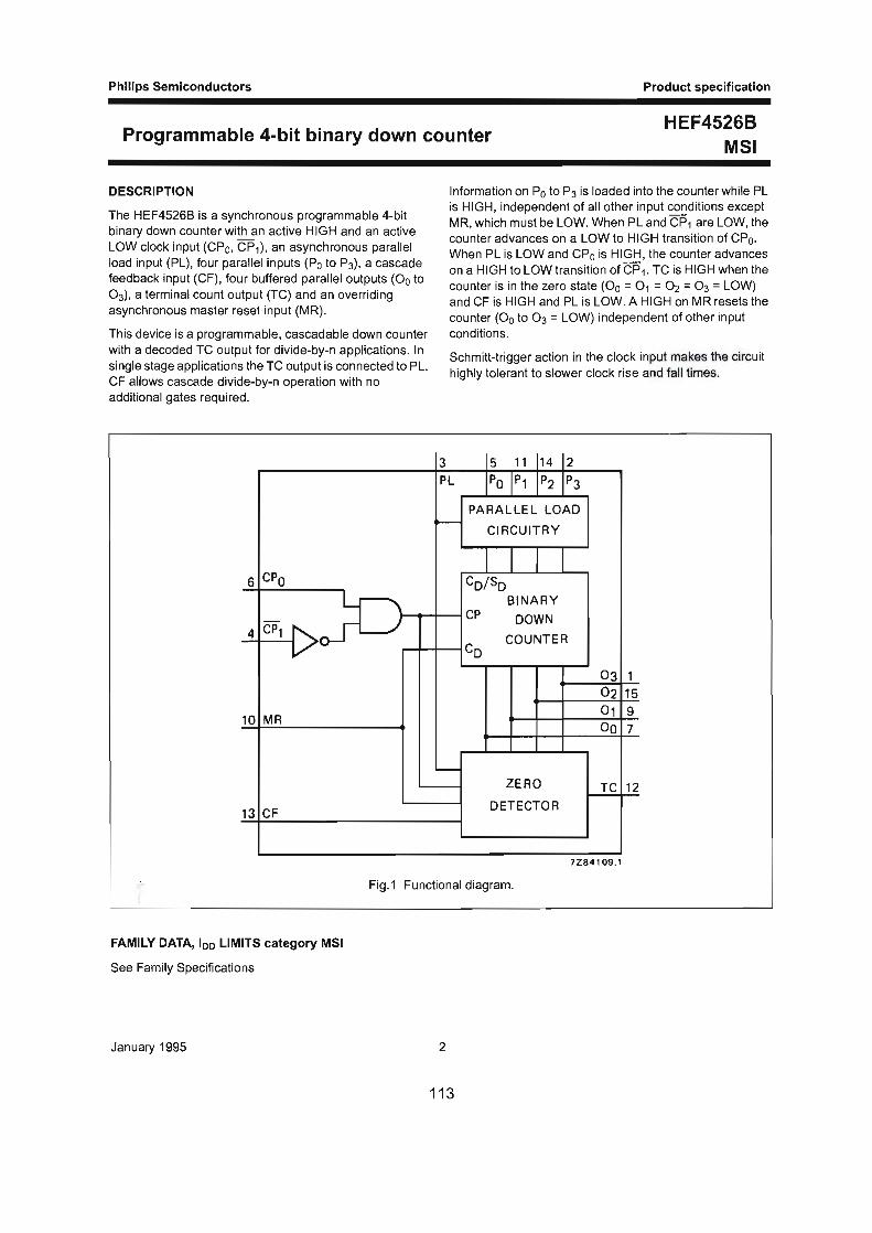
Philips Semiconductors Product specification
Programmable 4-bit binary down counter HEF4526B
MSI
DESCRIPTION
The HEF4526B is a synchronous programmable 4-bit binary down counter with an active HIGH and an active LOW clock input (CP0, CP1) , an asynchronous parallel load input (PL), four parallel inputs (Po to P3), a cascade feedback input (CF), four buffered parallel outputs (Oo to 0 3), a terminal count output (TC) and an overriding asynchronous master reset input (MR).
This device is a programmable, cascadable down counter with a decoded TC output for divide-by-n applications. In single stage applications the TC output is connected to PL. CF allows cascade divide-by-n operation with no additional gates required.
6 CPa
-4 cP1
10 MR
13 CF
3
Information on Po to P3 is loaded into the counter while PL is HIGH, independent of all other input conditions except MR. which must be LOW. When PL and CP1 are LOW, the counter advances on a LOW to HIGH transition of CPa. When PL is LOW and CP0 is HIGH, the counter advances on a HIGH to LOW transition of CP 1. TC is HIGH when the counter is in the zero state (Oo = o, = 02 = 03 = LOW) and CF is HIGH and PL is LOW. A HIGH on MR resets the counter (Oo to 0 3 = LOW) independent of other input conditions.
Schmitt-trigger action in the clock input makes the circuit highly tolerant to slower clock rise and fall times.
5 11 14 2
PL Po p1 p2 p3
PARALLEL LOAD r- CIRCUITRY
Co/So BINARY
CP DOWN
Co COUNTER
03 1
02 15
01 9 oo 7
'--
ZERO TC 12
DETECTOR
7Z84109.1
Fig.1 Functional diagram.
FAMILY DATA, 100 LIMITS category MSI
See Family Specifications
January 1995 2
113

Philips Semiconductors Product specification
Programmable 4-bit binary down counter HEF45268
MSI
PINNING
PL
Po to P3
CF
CPo
CP1
MR
TC
Oo to 03
HEF4526B
Fig.2 Pinning diagram.
parallel load input
parallel inputs
cascade feedback input
7Z74610
clock input (LOW to HIGH, triggered)
clock input (HIGH to LOW, triggered)
asynchronous master reset input
terminal count output
buffered parallel outputs
COUNTING MODE
CF = HIGH; PL = LOW; MR = LOW
OUTPUTS COUNT
03 02 01 Oo
15 H H H H
14 H H H L
13 H H L H
12 H H L L
11 H L H H
10 H L H L
9 H L L H
8 H L L L
7 L H H H
6 L H H L
5 L H L H
4 L H L L
3 L L H H
2 L L H L
1 L L L H
0 L L L L
January 1995 3
HEF4526BP(N): 16-lead OIL; plastic
(SOT38-1)
HEF4526BD(F): 16-lead OIL; ceramic (cerdip)
(SOT74)
HEF4526BT(D): 16-lead SO; plastic
(SOT109-1)
( ): Package Designator North America
FUNCTION TABLE
MR PL CP0 CP1 MODE
H X X X reset (asynchronous)
L H X X preset (asynchronous)
L L f H no change
L L L "\... no change
L L "\... X no change
L L X f no change
L L f L counter advances
L L H "\... counter advances
Notes
1. H =HIGH state (the more positive voltage) L =LOW state (the less positive voltage) X = state is immaterial f = positive-going transition "\._ = negative-going transition
114

Philips Semiconductors
Programmable 4-bit binary down counter
SINGLE STAGE OPERATION
Divide-by-n; MR = LOW; CF = HIGH; CP1 = LOW
PL p3 p2 p1 Po DIVIDE TC OUTPUT
BY PULSE WIDTH
L X X X X 16 one clock
period
TC H H H H 15
TC H H H L 14
TC H H L H 13
TC H H L L 12
TC H L H H 11
TC H L H L 10
TC H L L H 9
TC H L L L 8 clock pulse
HIGH TC L H H H 7
TC L H H L 6
TC L H L H 5
TC L H L L 4
TC L L H H 3
TC L L H L 2
TC L L L H 1
TC L L L L no operation
Fig.3 State diagram.
January 1995 4
115
7Z74616
Product specification
HEF4526B MSI
Philips Semiconductors
Programmable 4-bit binary down counter
oM-<J '
I I . r---' rl ... ~ n
v v ~
( l 1~1
-... I I I I ./H-i ...... n II _) I I . I I
I I I _ l I I
Product specification
II II f \ ( \
HEF4526B MSI
II I I !"""" ~
II I I I I I I I
~--+-----+-+---______.______._.__II 111 1 I 11 o<}r-J I ~___/] I l . l 11
r· ~ :!:N h Q, -vv---v1=f J II
- /1 I~ I I I I I ~ IN~ I f"\ I
~ r--... _ lr--... _ 1=~1
I ....__. I
January 1995 5
116
\ ) Il l I I 1 1 r ~ ' tl 'II I I I
I I I I II I ll
I ll
I
1u u

Philips Semiconductors
Programmable 4-bit binary down counter
AC CHARACTERISTICS
Vss = 0 V; lamb= 25 oc; input transition times~ 20 ns
Voo TYPICAL FORMULA FOR P (~-tW) v Dynamic power 5 1000 f; +I (f0 CL) x Voo2
dissipation per 10 4000 f; +I (f0 CL) x Voo2
package (P) 15 10 000 f; +I (foCL) x Voo2
AC CHARACTERISTICS
Vss = 0 V; lamb= 25 oc; CL =50 pF; input transition times~ 20 ns
Voo SYMBOL MIN. TYP. MAX. v Propagation delays
-CPo. CP1 ~On 5 150 300
HIGH to LOW 10 tPHL 65 130
15 50 100
5 150 300
LOW to HIGH 10 tPLH 65 130
15 50 100 -
CP0, CP, ~lC 5 210 420
HIGH to LOW 10 tpHL 90 180
15 70 140
5 210 420
LOW to HIGH 10 tpLH 90 180
15 70 140
PL~On 5 200 400
HIGH to LOW 10 tPHL 80 160
15 60 120
5 180 360
LOW to HIGH 10 tpLH 70 140
15 50 100
MR~On 5 140 280
HIGH to LOW 10 tpHL 55 110
15 40 80
Output transition times 5 60 120
HIGH to LOW 10 tTHL 30 60
15 20 40
5 60 120
LOW to HIGH 10 tTLH 30 60
15 20 40
January 1995 6
117
where
Product specification
HEF4526B MSI
f; = input freq. (MHz)
f0 = output freq. (MHz)
CL = load capacitance (pF)
I (f0 CL) = sum of outputs
Voo = supply voltage (V)
TYPICAL EXTRAPOLATION FORMULA
ns 123 ns + (0,55 ns/pF) CL
ns 54 ns + (0,23 ns/pF) CL
ns 42 ns + (0,16 ns/pF) CL
ns 123 ns + (0,55 ns/pF) CL
ns 54 ns + (0,23 ns/pF) CL
ns 42 ns + (0,16 ns/pF) CL
ns 183 ns + (0,55 ns/pF) CL
ns 79 ns + (0,23 ns/pF) CL
ns 62 ns + (0,16 ns/pF) CL
ns 183 ns + (0,55 ns/pF) CL
ns 79 ns + (0,23 ns/pF) CL
ns 62 ns + (0, 16 ns/pF) CL
ns 173 ns + (0,55 ns/pF) CL
ns 69 ns + (0,23 ns/pF) CL
ns 52 ns + (0, 16 ns/pF) CL
ns 153 ns + (0,55 ns/pF) CL
ns 59 ns + (0,23 ns/pF) CL
ns 42 ns + (0, 16 ns/pF) CL
ns 113 ns + (0,55 ns/pF) CL
ns 44 ns + (0,23 ns/pF) CL
ns 32 ns + (0,16 ns/pF) CL
ns 10 ns + (1 ,0 ns/pF) CL
ns 9 ns + (0,42 ns/pF) CL
ns 6 ns + (0,28 ns/pF) CL
ns 10 ns + (1 ,0 ns/pF) CL
ns 9 ns + (0,42 ns/pF) CL
ns 6 ns + (0,28 ns/pF) CL

Philips Semiconductors
Programmable 4-bit binary down counter
AC CHARACTERISTICS
Vss = 0 V; lamb= 25 oc; CL =50 pF; input transition times :::; 20 ns
Voo SYMBOL MIN. TYP. v Minimum clock 5 80 40
pulse width CP0 10 twcPL 40 20
LOW 15 30 15
Minimum clock 5 80 40 -
pulse width CP1 10 twcPH 40 20
HIGH 15 30 15
Minimum PL 5 100 50
pulse width; HIGH 10 twPLH 40 20
15 32 16
Minimum MR 5 130 65
pulse width; HIGH 10 twMRH 50 25
15 40 20
Hold time 5 30 5
Pn ~ PL 10 !hold 20 5
15 15 5
Set-up time 5 30 0
Pn ~ PL 10 lsu 20 0
15 15 0
Maximum clock 5 6 12
pulse frequency 10 fmax 12 25
PL =LOW 15 16 32
Note
MAX.
ns
ns
ns
ns
ns
ns
ns
ns
ns
ns
ns
ns
ns
ns
ns
ns
ns
ns
MHz
MHz
MHz
Product specification
HEF4526B MSI
see also waveforms Figs 5 and 6
see note 1
1. In the divide-by-n mode (PL connected to TC), one has to observe the maximum HIGH to LOW propagation delay for CP to TC, before applying the next clock pulse.
January 1995 7
118

Philips Semiconductors
Programmable 4-bit binary down counter
PLINPUT
PniNPUT
On OUTPUT
tPLH li.-/50%
------J
--''"'\.._______
7Z84145
Product specification
HEF45268 MSI
Fig.5 Waveforms showing minimum PL pulse width, propagation delays for PL, Pn to On and hold time for PL to Pn.
CPo INPUT
cP1 INPUT
on OUTPUT
TC OUTPUT
_j
--
I \ 50%
\ I -twcPL--
/50%
I -tPLH -/50%
I ~tPLH --
I
I \ 50%
I \ -twcPH--
\ \ I
tPHL - - tPLH .-
\ \
tPHL 7Z84144 .-
Fig.6 Waveforms showing minimum CPa and CP1 pulse widths, propagation delays for CPa, CP 1 to On and TC.
January 1995 8
119
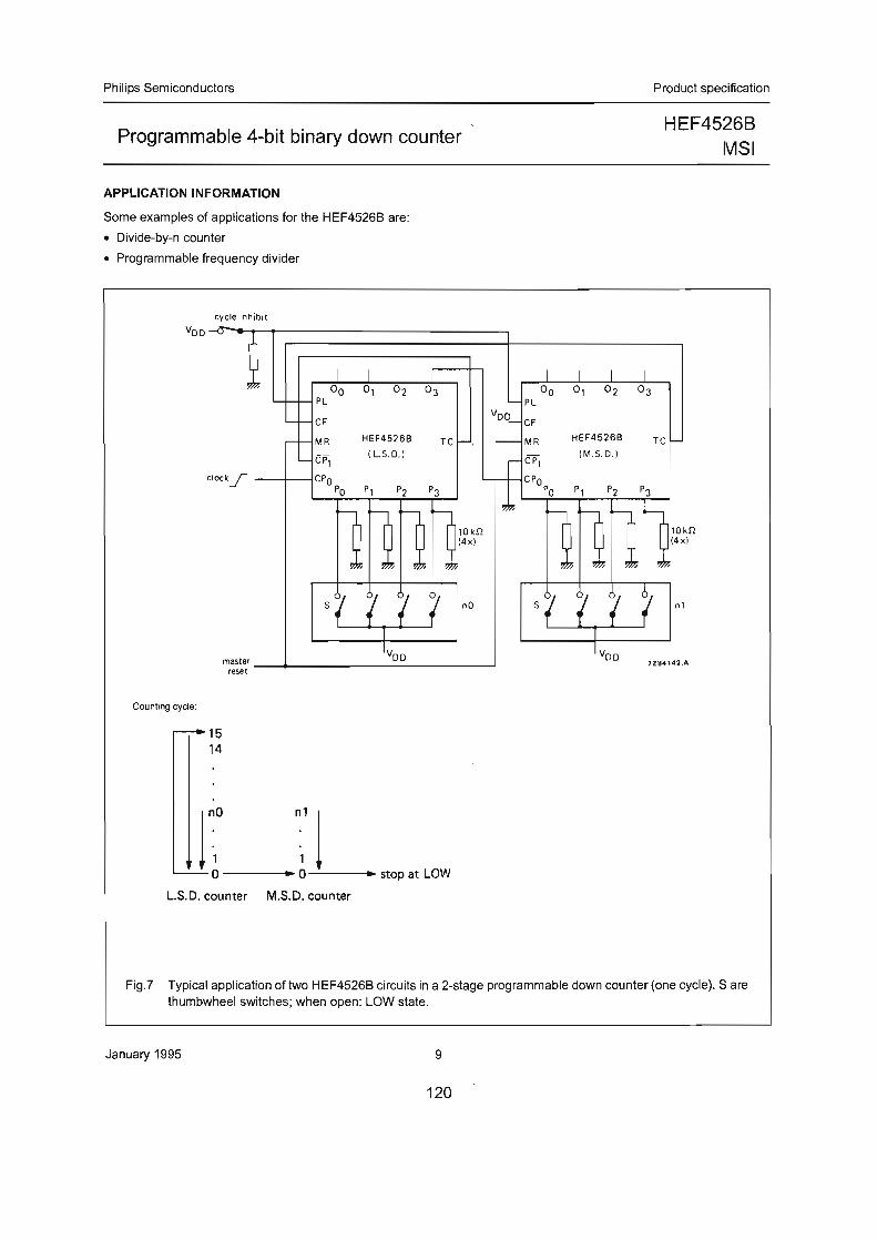
Philips Semiconductors
Programmable 4-bit binary down counter
APPLICATION INFORMATION
Some examples of applications for the HEF4526B are:
• Divide-by-n counter
• Programmable frequency divider
Counting cycle:
cycle inhibit
clockJ --+---1
15 14
s
r ";' 1 0 ------t., 0---- stop at LOW
L.S.D. counter M.S.D. counter
HEF4526B
(M.S. D.)
Product specification
HEF4526B MSI
nl
7Z8414'2.A
Fig.7 Typical application of two HEF4526B circuits in a 2-stage programmable down counter (one cycle). S are thumbwheel switches; when open: LOW state.
January 1995 9
120
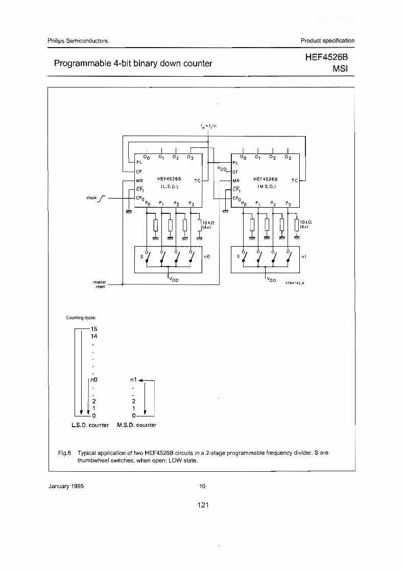
Philips Semiconductors
Programmable 4-bit binary down counter
Counting cycle:
15 14
r; ";] 0 0
L.S.D. counter M.S. D. counter
HEF4526B
( L.S. 0 . 1
HEF4526B (M.S. D. I
Product specification
nl
7Z84143.A
HEF4526B MSI
Fig.8 Typical application of two HEF4526B circuits in a 2-stage programmable frequency divider. S are thumbwheel switches; when open: LOW state.
January 1995 10
121

IRF 140 HEXFET Power Mosfet datasheet ANNEXURE C
=,..,.. = 1111
SEME IRF140
LAB MECHANICAL DATA Dimensions in mm (inches)
-~~~J~.~ -i!!L 3.64 (0.1 !f1) .
d if.l. 2 plcs.
3Q.4.()_(1 .197)._ ,. _ .. ... 30.15 (1 .187) i
.. 17.15 (0 .67~-J I 18.64 (0.655) I
N-CHAN'NEL POWER MOSFET
Voss
lo(cont)
Ros(on)
FEATURES
100V 28A
0.077Q
• HERMETICALLY SEALED T0-3 METAL PACKAGE
~(0.800) ..
I 18.80 (0.740J i dia. ~~~
• SIMPLE DRIVE REQUIREMENTS
e.£. • SCREENING OPTIONS AVAILABLE
Pin 1- Gate
~"'
r~~ ,~ ~ e.s I I>?!
1.09 (0 .043) 0.97 (0.038)
dia. 2 plc:s. -----~· ~~
T0-3 Metal Package Pin 2 - Source Case- Drain
ABSOLUTE MAXIMUM RATINGS (T case= 25°C unless otherwise stated)
EAs
IAR
EAR
dv/dt
TJ, Tstg
TL
Notes
Gate- Source Voltage
Continuous Drain Current
Continuous Drain Current
Pulsed Drain Current 1
(VGs = 0 • Tease= 25oC)
(VGs = 0 , Tease= 100oC)
Power Dissipation @ T case = 25°C
Linear Derating Factor
Single Pulse Avalanche Energy 2
Avalanche Current 2
Repetitive Avalanche Energy 2
Peak Diode Recovery 3
Operating and Storage Temperature Range
Lead Temperature 1.6mm (0 .63") from case for 10 sec.
1) Pulse Test: Pulse Width :s; 300~s. o :s; 2% 2) @ V00 = 25V, L ~ 480~H, RG = 250, Peak IL = 28A, Starting TJ = 25oC 3) @ lso :s; 28A, di/dt :s; 170NJ..1s, V00 :s; BVoss, TJ :s; 150°C, Suggested RG = 9.1n
Semelab pic. Telephone (01455) 556565. Telex: 341927. Fax (01455) 552612.
122
±20V
28A
20A
112A
125W
1W/"C
250mJ
28A
12.5mJ
5.5V/ns
-55 to +150°C
300oC
Prelim. 9/96

1111 =~= - -- -1111
SEME
LAB ELECTRICAL CHARACTERISTICS (Tease= 2soc unless otherwise stated)
Parameter Test Conditions Min.
STATIC ELECTRICAL RATINGS
BVoss Drain -Source Breakdown Voltage VGs = 0 10 = 1mA 100
6BVoss Temperature Coefficient of Reference to 25°C
6TJ Breakdown Voltage 10 = 1mA
Static Drain - Source On-State VGs = 10V 10 = 20A Ros(on) -·--····-·
Resistance 1 VGs = 10V 10 = 28A
VGS(th) Gate Threshold Voltage Vos = VGs 10 = 250mA 2 - ··--- - ···
gfs Forward Transconductance 1 V0 s ~ 15V los = 20A 9.1
VGs = 0 V0 s = 0.8BVoss loss Zero Gate Voltage Drain Current -
TJ = 125°C
IGss Forward Gate -Source Leakage VGs = 20V
IGss Reverse Gate - Source Leakage VGs = -20V
DYNAMIC CHARACTERISTICS
Ciss Input Capacitance VGs = 0
Coss Output Capacitance Vos = 25V --
Crss Reverse Transfer Capacitance f = 1 MHz
~g Total Gate Charge VGs = 10V 30 -· -
Ogs Gate - Source Charge 10 = 28A 2.4
<::}gd Gate - Drain ("Miller") Charge Vos = 0.5BVoss f-· 12
td(on) Turn-On Delay Time v00 = 50V
tr Rise Time - ·····-· ····--- 10 = 28A ~(off) Turn-Off Delay Time
tf Fall Time RG=9.1!1
SOURCE- DRAIN DIODE CHARACTERISTICS
Is Continuous Source Current
IsM Pulse Source Current 2
Vso Diode Forward Voltage 1 Is= 28A TJ = 25°C
VGs"' 0 -trr Reverse Recovery Time IF= 28A TJ = 25°C
Orr Reverse Recovery Charge 1 di I dt ~ 1 OOA!).lS V oo ~ 50V -ton Forward Turn-On Time
PACKAGE CHARACTERISTICS
Lo Internal Drain Inductance (measured from 6mm down drain lead to centre of die) --
Ls Internal Source Inductance (from 6mm down source lead to source bond pad)
THERMAL CHARACTERISTICS
ReJC Thermal Resistance Junction - Case
Recs Thermal Resistance Case - Sink
RaJA Thermal Resistance Junction - Ambient
Notes 1) Pulse Test: Pulse Width ~ 300ms, o ~ 2% 2) Repetitive Rating -Pulse width limited by maximum junction temperature.
Semelab pic. Telephone (01455) 556565. Telex: 341927. Fax (01455) 55261 2.
123
IRF140
Typ. Max. Unit
v -
0.13 V /°C
0.077 -0.089
n
4 v -
S (U)
I _L 25 llA 250
100 - · nA
-100
1660
I 550 pF
120
59 ·-
12 nC
30.7
21 --145
-21
ns
105
28 A
l I 112
1.5 v
I 400 ns --
2.9 !lC
Negligible
5.0 -- -r---- - nH 13
1.67
0.12 oc/W '
30
Prel im. 9/96
HEF 40106 HEX inverting Schmitt trigger datasheet ANNEXURE D
INTEGRATED CIRCUITS
For a complete data sheet, please also download:
• The IC04 LOCMOS HE4000B Logic Family Specifications HEF, HEC
• The IC04 LOCMOS HE4000B Logic Package Outlines/Information HEF, HEC
HEF40106B gates Hex inverting Schmitt trigger
Product specification File under Integrated Circuits, IC04
Philips Semiconductors
124
January 1995
PHILIPS

Philips Semiconductors
Hex inverting Schmitt trigger
DESCRIPTION
Each circuit of the HEF401 068 functions as an inverter with Schmitt-trigger action. The Schmitt-trigger switches at different points for the positive and negative-going input signals. The difference between the positive-going voltage (Vp) and the negative-going voltage (VN) is defined as hysteresis voltage (VH).
This device may be used for enhanced noise immunity or to "square up" slowly changing waveforms.
1 11 I \l_ L.. o1 2 I I
3 121 \l_ "'
02
4
1 r
5 131 \l_ L.. 0 3 6
I I
14 I \l_ L... o4 9 8
I J
1 1 1si\L L 0 s 10
1 r 13 1s I \l_ L 0
6 12 I _r
7Z74608.1
Fig.1 Functional diagram.
January 1995 2
Product specification
HEF40106B gates
HEF40106B
Fig.2 Pinning diagram.
HEF40106BP(N): 14-lead DIL; plastic
(SOT27-1 )
7Z74609
HEF40106BD(F): 14-lead DIL; ceramic (cerdip)
(SOT73)
HEF401 06BT(D): 14-lead SO; plastic
(SOT108-1)
( ): Package Designator North America
Fig.3 Logic diagram (one inverter).
FAMILY DATA, 100 LIMITS category GATES
See Family Specifications
125

Philips Semiconductors
Hex inverting Schmitt trigger
DC CHARACTERISTICS
Vss == 0 V; Tamb == 25 oc
Hysteresis
voltage
Switching levels
positive-going
input voltage
negative-going
input voltage
-1 VH 1- Vr
Voo v 5
10
15
5
10
15
5
10
15
VN Vp 7Z0999S.l
Fig.4 Transfer characteristic.
January 1995
Product specification
HEF40106B gates
SYMBOL MIN. TYP. MAX.
VH
Vp
VN
3
126
0,5 0,8 v 0,7 1,3 v 0,9 1,8 v 2 3,0 3,5 v
3,7 5,8 7 v 4,9 8,3 11 v 1,5 2,2 3 v 3 4,5 6,3 v 4 6,5 10,1 v
v-~---v-~ \ ~
7Z84130.1
Fig.5 Waveforms showing definition of Vp, VN and VH. where VN and Vp are between limits of 30% and 70%.

Philips Semiconductors
Hex inverting Schmitt trigger
AC CHARACTERISTICS
Vss = 0 V; Tamb = 25 ac; CL =50 pF; input transition times~ 20 ns
Voo SYMBOL TYP. v Propagation delays
In~ On 5 90
HIGH to LOW 10 tPHL 35
15 30
5 75
LOW to HIGH 10 tPLH 35
15 30
Output transition times 5 60
HIGH to LOW 10 tTHL 30
15 20
5 60
LOW to HIGH 10 tTLH 30
15 20
MAX.
180 ns
70 ns
60 ns
150 ns
70 ns
60 ns
120 ns
60 ns
40 ns
120 ns
60 ns
40 ns
Product specification
HEF40106B gates
TYPICAL EXTRAPOLATION FORMULA
63 ns + (0,55 ns/pF) CL
24 ns + (0,23 ns/pF)
22 ns + (0,16 ns/pF) CL
48 ns + (0,55 ns/pF) CL
24 ns + (0,23 ns/pF) CL
22 ns + (0,16 ns/pF) CL
10 ns + (1,0 ns/pF) CL
9 ns + (0,42 ns/pF) CL
6 ns + (0,28 ns/pF) CL
10 ns + (1,0 ns/pF) CL
9 ns + (0,42 ns/pF) CL
6 ns + (0,28 ns/pF) CL
Voo TYPICAL FORMULA FOR P (J.tW) v Dynamic power 5 2 300 f; + L (f0 CL) x Voo2 where
dissipation per 10 9 000 f; + L (foCL) x Voo2 f; = input freq. (MHz)
package (P) 15 20 000 f; + L (f0 CL) x Voo2 f0 =output freq. (IMHz)
CL = load capacitance (pF)
L (foCL) = sum of outputs
V00 =supply voltage (V)
January 1995 4
127

Philips Semiconductors
Hex inverting Schmitt trigger
100
50
0 0
"' -v
7284167
I I
1/ 'I
J\ \
' 2,5 5
Fig.6 Typical drain current as a function of input voltage; Voo = 5 V; T am b = 25 °C.
2000
1000
0 0
/
J
I I
7284169
I iJ 1/\
\ \.
' 10 vi (Vl 20
Fig.B Typical drain current as a function of input voltage; Voo = 15 V; T amb = 25 oc.
January 1995 5
128
1000
I 500 II
J
'-.. I ~ ~
/ /v
5
Product specification
HEF40106B gates
7284168
i
"": ." vi (Vl 10
Fig.7 Typical drain current as a function of input voltage; Voo =10 V; l amb = 25 °C.

Philips Semiconductors
Hex inverting Schmitt trigger
10
Vp ,/
:..,..... 17'
/ v 5
,/ ,., .... ,/ ,.,
./ v i.,.....- v v !.,...--
,.,.. 1/~
I/
!.,...--
v v
~ v !.,...-- j...-"
...... ~ v v
f..' VN
I' _.,.
Product specification
HEF40106B gates
7Z84183
1,.-
v
L....- 1,..
l,..-- . I
I
'
0 2,5 7,5 12,5 Voo (Vl 17,5
Fig.9 Typical switching levels as a function of supply voltage V00; Tamb = 25 oc.
Cp
r---H----, I I
HI l_ l R \L riC,......_._-----c:r-
... L.. c
I 7Z84165
Fig.1 0 Schmitt trigger driven via a high impedance (R > 1 kfl) .
If a Schmitt trigger is driven via a high impedance (R > 1 kfl) then it is necessary to incorporate a capacitor C of such
C V o - Vss value that: C >
0 , otherwise oscillation can occur on the edges of a pulse.
p VH Cp is the external parasitic capacitance between input and output; the value depends on the circuit board layout.
January 1995 6
129
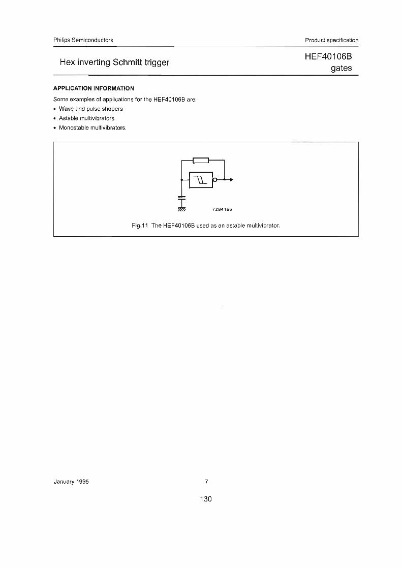
Philips Semiconductors
Hex inverting Schmitt trigger
APPLICATION INFORMATION
Some examples of applications for the HEF40106B are:
• Wave and pulse shapers
• Astable multivibrators
• Monostable multivibrators.
7Z84166
Fig.11 The HEF401 068 used as an astable multivibrator.
January 1995 7
130
Product specification
HEF40106B gates

IRF 610 HEXFET Power Mosfet datasheet
I :te)R I Rectifier HEXFEr® Power MOSFET
• Dynamic dv/dt Rating • Repetitive Avalanche Rated • Fast Switching • Ease of Paralleling • Simple Drive Requirements
Description Third Genera~on HEXFETs from lntemational Rectifier provide the designer with the best combination of fast switching, ruggedized device design, low on-resistance and cost-effectiveness.
The T0-220 package is universally preferred for all commercial-industrial applications at power dissipation levels to approximately 50 watts. The low thermal resistance and low package cost of the T0-220 contribute to its wide acceptance throughout the Industry.
Absolute Maximum Ratings Parameter
lo@ Tc=25•C Continuous Drain Current, VGs@ 10 V
lo@ Tc = 10o•c Continuous Drain Current, VGs @ 10 V
I oM Pulsed Drain Current CD
Po@ Tc =2S•c Power Dissipation
Linear Derating Factor
Vos Gate-to-Source Voltage
EAs Single Pulse Avalanche Energy_ <2l IAR Avalanche Current CD
EAR Repetitive Avalanche Energy CD dv/dt Peak Diode Recovery dv/dt <ll
ANNEXURE E
IRF61 0
Voss= 200V
RDs(on) = 1.5n
10 = 3.3A
TQ-220AB
Max. Units
3.3
2.1 A
10
36 w 0.29 W/"C
±20 v 64 mJ
3.3 A
3.6 mJ
5.0 V/ns
TJ Operating Junction and -55 to +150 TsTG Storage Temperature Range ·c
Soldering Temperature, for 10 seconds 300 (1 .6mm from case) Mounting Torque, 6-32 or M3 screw 101bf.ln(1.1 Nom)
Thermal Resistance
Parameter Min. TY£:. Max. Units
Rruc Junction-to-Case - - 3.5
Roes Case-to-Sink, Flat, Greased Surface - 0.50 - •cfW --RtJJA Junction-to-Ambient - - 62 ---
131

IRF610 Electrical Characteristics@ TJ = 25°C (unless otherwise specified)
Parameter
VtBR)DSS Drain-to-Source Breakdown Vokage
llVtBR)Oss/LITJ Breakdown Voltage Temp. Coefficient
Ros(on) Static Drain-to-Source On-Resistance
VaS(Ihl Gate Threshold Voltage
gts Forward Transconductance
loss Drain-to-Source Leakage Current
lass Gate-to: Source Forward Leakage
Gate-to-Source R401verse Leakag_e
Ov Total Gate Charge
Ogo Gate-to-Source Charge
Qgd Gate-to-Drain ('Miller") Charge
ldton) Turn-On Delay Time
tr Rise Time
ldtor~ Tum-Off Delay Time
t, Fall Time
Lo Internal Drain Inductance
Ls Internal Source Inductance
C;ss Input Capacitance
Coss Output Capacitance
Crss Reverse Transfer Capacitance
Source-Drain Ratings and Characteristics
Is
Vso
trr
Orr lon
Notes:
Parameter
Continuous Source Current (Body Diode)
Pulsed Source Current (Body Diode) CD Diode Forward Voltage
Reverse Recovery Time
Reverse Recovery Charge
Forward Tum-On Time
I
Min. Typ. Max. Units Test Conditions
200 - - v Vas=OV, loE 250!.LA
- 0.30 - V/"C Reference to 2s•c, lo= 1mA
- - 1.5 n VGs=10V, lo=2.0A ® 2.0 - 4.0 v I Vos=VGS, lo= 250f.LA
0.80 - - s . Vos=sov, lo=2.0A ® - - 25
!lA Vos=200V, VGS=OV
- - 250 Vos=160V, VGs=OV, TJ=12S•C
- - 100 nA
,Vas=20V
- - -100 VGS=-20V
- - 8.2 lo=3.3A
- - 1.8 nC Vos=160V
- - 4.5 Vas=10V See Fig. 6 and 13 ®
- 8.2 - Voo=100V
- 17 - lo=3.3A ns - 14 - Ra=24n
- 8.9 - Ro=300 See Rgure 1 o ®
4.5 Between lead, .@ - - 6 mm (0.25in.)
nH from package - 7.5 - and center of
die contact • - 140 - VGs=OV
- 53 - pF Vos=25V
- 15 - f=1.0MHz See Figure 5
Min. Typ. Max. Units Test Conditions
A 3.3 MOSFET symbol ~o
showing the
integral reverse G
p-n junctron diode. s 10 1
2.0 v T r25•C, ls=3.3A, VGs=OV ®
- 150 310 ns Tr2s•c, IF=3.3A
- 0.60 1.4 J.LC di/dt=100AIJ.LS ® Intrinsic tum-on time Is neglegible (tum-on Is dominated by Ls+Lo)
CD Repetitive rating: pulse width limited by max. junction temperature (See Figure 11)
@ lsos3.3A, dVdt:S70AIJ.LS, Voo:SV(BR)OSS, TJs1so· c
<Z> Voo=50V, starting TJ=2s•c, b•8.8mH Ro=25n, 1As=3.3A (See Figure 12)
@) Pulse width s 300 11s: duty cycle S2"1o.
132
'

10 I '" '" ::: t:: ......
IOTTOM ::::
~ .,
~ .~v~ 4.5Y
L 20u s 'plA_sE WIDTH
Tc a 25oc
to 1 toO to'
Vos. Drain-to-Source Voltage (volts)
Fig 1. Typical Output Characteristics, Te=25°C
..;
...? v 0
,v 1/
I I
2
Vos • 50V 20us PU.SE WIDTH
10
VGs. Gate-to-Source Voltage (volts)
Fig 3. Typical Transfer Characteristics
IRF61 0
... ,.,.. ... "' 1 , 0 \1 ' 1.0'11 , • . 0 11 . .. , .ov
~ E too ~
IOTJOM 4, 11V
~
'E ~ :l
' ... (.) 4.5Y c: "i§ 0 10" ..9 ·:ulll I
.1/ "'/ II 20us PLLSE WIDTH
It Tc - tsooc ' to t toO to '
Vos. Drain-to-Source Voltage (volts)
Fig 2. Typical Output Characteristics, Tc-1sooc
3.5
3 .0
2.5 c: o~
B i 2.o ~ 14 0"'
CJ? E 0 0 1.5 -;-z c: ~ ·n; 0 1.0
~ 0.5
10 • 3 .JA
v
'
v v
v v
....... I
:,....--
VGS • 10V
I
(/) 0
a: o.o_60 - •o -20 o zo •o so eo too 120 t•o t60
TJ, Junction Temperature (°C)
Fig 4. Normalized On·Resisance Vs. Temperature
133
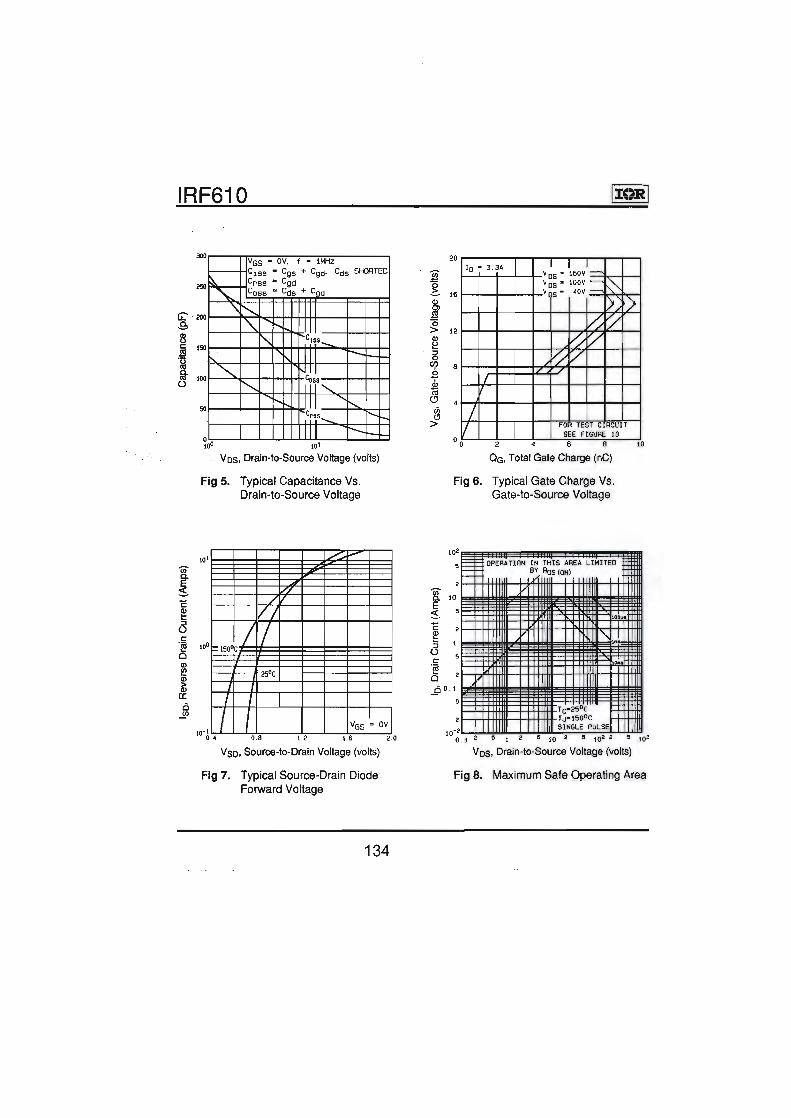
IRF610
30 0
G:'200 .9: 8 c 150 . .m
~ 100 0
r--
~ '\
""-.._
VGS • OV. f • 1MHz C 1 ss • Cgs + Cgd· Cds SHOAT ED Crss • Cgd Ce ss • Cds + Cgd
t'.... II '\. ..... IJ
I' Ciss....,
II r-- -I-
['-... ~e ll I jj' '-
..... 1_11 1'-. Crss....._ f'--r--
II r--t-r-0 tOo tal
Vos, Draln·to-Source Voltage (volts)
Fig 5. Typical Capacitance Vs. Drain-to-Source Voltage
10 I .......:: 1--
//
/ VI
t5o0cL j 25°c
I I 1 I
I I I VGS = OV 0 .8 1.2 1.6
Vso. Source-to-Drain Voltage (volts)
Fig 7. Typical Source-Drain Diode Forward Voltage
2.0
134
'il:C)RI
20
~ _g_
16 (J)
~ 0 > 12
~
r0 • 3.3A I I I v 05 • 16ov = Vog•100V~ ~ V S • 40V ~
~- ) ~ t/
/./ / " 0
~ 8
";'
* ~ /
I I
C}
cil (.')
> I v FO l EST C RCU!T
SEE F !GURE 13
2 6 10
OG. Total Gate Charge (nC)
Fig 6. Typical Gate Charge Vs. Gate-to-Source Voltage
to> oE ~
:OPERA TlON' ~~- !H-IS AREA LIMIT EO
2
10 11 1
" 2 ',
I
" 2
k' . 1
" Ill : c·:; 'c
2
IIIII SINGLE PULSE ' 0
2 • 2 2 • 0 . 1 10 10
Vos. Drain-to-Source Voltage (volts)
Fig 8. Maximum Safe Operating Area

• . 0
~ 3 .0 r-....
~
Oi - 2.0
0.0 25
:-... r-:-...
~'-... ...... ['._
'~
""' 50 75 100 125
T c. Case Temperature (°C)
\ 150
IRF61 0 Ro
D.U.T .
:voo
Fig 10a. Switching Time Test Circuit
Vos 90%----~f---------~----~-
. 10%--~-+--~-------+~~-rVGs
tcl(on) t,
Fig 9. Maximum Drain Current Vs. Fig 10b. Switching Time Waveforms Case Temperature
10
J <I)
"' <::
io-•·
... ~~ 8. "' <I)
a: ... ...... ' ·' ~
1il E 0 . 1 Gl
F
I SINGLE PULSE I I I .... O. Oi
(THEAAAL RESPONSE)
~ ~ ... .1
NOTES: l. DUTY FACTOR. O•t 1/t2
2 2 . PEA~ .T)•PoH x Zth)C • l c
-10-
10..., 10 • w-• w-• 0 . 1 10
t1, Rectangular Pulse Duration (seconds)
Fig 11. Maximum Effective Transient Thermal Impedance, Junction-to-Case
135

IRF610
Vary 1p to obtain required lAs
L
O.OHl
+ Voo
Fig 12a. Unclamped Inductive Test Circuit
r- V(BA)DSS
r--'P ----1
Vos
I Voo
I \ / I \ I \ I [! \ -- -----lAS
Fig 12b. Unclamped Inductive Waveforms
Charge -
Fig 13a. Basic Gate Charge Waveform
I >. ~ Q) .:: w 3l :; n. Q)
Ol .::
U5 u, < w
140 ro
120 ~ TOP LOA
2 . 1A BOTTOM 3 .3A
100 ~ \ I
BO '\ [\ -~ ~
60 1\.
' .~ '\ I
40 " ~ D:,
" "' I 20 """' I I'-. ~
voo • sov I ~ ~ 25 50 75 100 125 ISO
Starting TJ, Junction Temperature(0 C)
Fig 12c. Maximum Avalanche Energy Vs. Drain Current
IG lo Curren! Sampling Aesll!ore
+ _vos
Fig 13b. Gate Charge Test Circuit
Appendix A: Figure 14, Peak Diode Recovery dv/dt Test Circuit- See page 1505
Appendix B: Package Outline Mechanical Drawing- See page 1509
Appendix C: Part Marking Information- See page 1516
Appendix E: Optional Leadforms - See page 1525
136
lntemational I :r<)R I Rectifier

~
~ ;::J X U-1
~ <e:
..... (]) ;>
·;:::: "'0 ..... ~ Vl 0
2 ;;.-. u t:: (])
::l cr (])
¢::: I
..c tlJ)
:.a (])
..c ..... 4-< 0
~ .....
-~ "'0 ."'.::::: ::l u .::: u
1N4004 ~
IC3 7806T
~" vo I' I~
C12 ...I.,;
""i'1oo nF
GND
IC10 taoar
~VI vop I ll~
C14 ...I.,;
"'T1oo nF
GND
IC11 7812T
L_____-,----:1 VI VO r I I GND
C18 ....... '1oo nF
VCC-15V
_5)
L..C13 1 100 nF
C15 _J.,;
""T1oo nF
C19 ...I...
""T1oo nl=
a> a:.,....ln
;!;lo ~
...... ,,~ ~!I'll "
~ Lt:::...J
vee -6V
J Nil«> :n; Ci:Y~ n:y~ tDl
00 , I(~(· 02 15 c::::J.- 3
Ol 1
~o., rl ~ll<e Q: ~ ~~~~ il:Y~
" 11
~ 2
~ DP<l DP1 DP2 DF'l 8
:SI~ ......, "' i3 CF
~ ~I§ ~~~ ~~~ PE I I l PE
"'~ · "()'" 1 1
- R9 IC1 P IC2P IC4P IC5P
~ ~Y~ I .<::. <0 5
" ~
~ "'r~
;J;~ !;10 z
~!p j_C16
~~~ T1oo nF
N
"'r"'
GND
f--='I~ IC7P ..J..C17
~~~ T1oonF
G~D
11
12
IC2
PI Q4 I 7 11 05 t-c- I I 06 07 oa
"" 010 012
6~~ ~__,, -
4060N R7
820k 01
L f-c10 1 10 6,4 MHZ C8 ~~ C9 t
5-15pF T3
_3
oF 5-15pF
Test Point B
Test Pomt A
C5 ...I.,;
--r330nF
....L..C4
GND
SIGIN PC2
5 ex
-l-C7
"""T""'3.3oF :Qt,Ja
_.L GND
C.X VCOIN
INH PfO Rl DEMO l" R2 ZEN 'l
vee- 15V Test Point 0 Test PointE Test Point F Test Point G _2_
13 ~ TIP31C T1
~PointH
l
ao! 01 ~~. 02 1 Ol
·o- 12
~ N N
II u..IIN 0 0 8
0 ..J..C3
-.r ~ T470nF
"' "'
Test Point 1
1,5uH J L1 ~~
~y~ Output to
Mosfet Gate
r--{'f")

Printed circuit board of the high-frequency Mosfet driver ANNEXUREG
138

The completed high-frequency Mosfet driver ANNEXUREH
~ .. " ..... ,.. .,.,f!l'~l · j ·---~.:--· : . ' .
139