Embed Size (px)
Citation preview
Design and Demonstration of Relay
VLSI Circuits
Vladimir Stojanović (MIT)
in collaboration with
Elad Alon, Tsu-Jae King Liu (UC Berkeley)
Dejan Marković (UCLA)

2
Relay design evolution
2 2

3
Power-gating CMOS with relays
S D
B
GG
G G
55
μm
85μm
0
0.4
0.8
1.2
VD
D (
V)
-0.1 -0.05 0 0.05 0.10
1
2
3
0.15
Time (s)
Syn
c CM
OS (
V)
5
6
7
8
VG (
V)
DV
G =
2V
Vb
VH
R OSC
COSCR1
R2
C1
C2 External pulse gen
VG
VDD
to CMOS logic
A
VEXT,R
Power gate
Self-driven pulse generator
0 0.5 1 1.5 2 2.5 3 3.50
2
4
6
8
Time (s)
Vol
tage
(V)
3% Duty Cycle
Power-gating input (VOSC)
Gated CMOS VDDFariborzi et al.
CICC 2010

4
Energy gain over CMOS limited to large Toff
Energy gain G
Large Toff
Switching overhead negligible
32 45 65 90 130 180 25010
1
102
103
104
105
106
107
108
Technology node (nm)
To
ff (s)
1
2
5
10
VIO=VEXT,MVIO=VNOM
Energy gain
,on M off offM
R DD on
kR I TEG
E V T
CMOS LOGIC
VEXT,M
sleep VIO
VEXT,R
sleep VG
CMOS LOGIC
(a) (b)
VDDVDD
βCL βCLp L, , f ,C
p L, , f ,C
eCRγCM
CM CR
VEXT,M

5
Area savings more significant
10-2
10-1
100
101
102
10-6
10-5
10-4
10-3
10-2
10-1
100
101
102
I on [
A/m
m2]
Relay 10s 10k
Relay 1ms 10k
Relay 10s 1k
Relay 1ms 1k
Ton Ron,R
MOS 10s 1%
MOS 1ms 1%
MOS 10s 10%
MOS 1ms 10%
Ton overhead
MOS technology node and relay device pitch [m]
Current
Relay
Scaled
Relay
90nm
CMOS
Peak
Current
density
Relays fabricated in metal backend - no area overhead
Today: 1 mA/mm2 (ready for low-power apps)
Scaled: 10-100 mA/mm2 (ready for high-power apps)

6
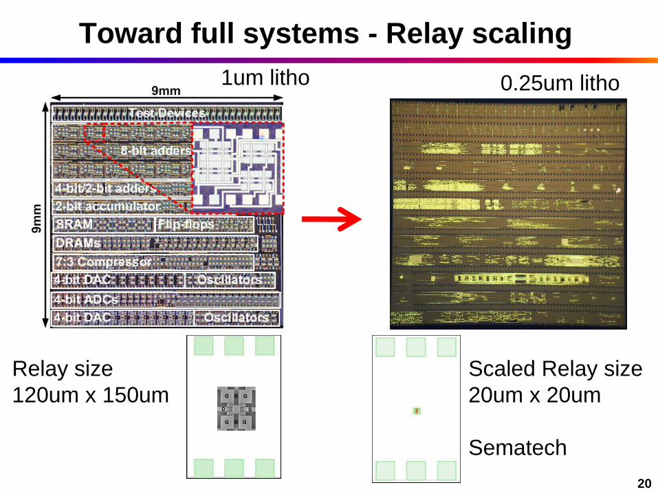
Relay VLSI chip platform
Test Devices
Logic
Timing
Elements
Memory
I/O
F. Chen et al, ISSCC2010
M. Spencer et al, JSSC Jan’11

7
Measured inverter VTC
VTC looks digital, suggests composability

8
Relay latch shows composability
Designed as if we used MOSFETS, but that isn’t optimal…

9
Oscillator illustrates delay characteristics
Mechanical time constant (tmech) >> electrical (telec)
Contact resistance only affects telec, not tmech
*Kam, et al. IEDM ‘09

10
Relay full adder
Demonstrates functional relay full-adder with
complementary devices
A
B
CinA
Cin
A
B
Vdd
A
B
A
B
Cout
kill
generate
propagate
Vdd
A
B
A
B
Cout
generate
kill
propagate
B
A
Vdd
Vdd
S
Time (s)V
olt
ag
e (
V)
48
1216
S
48
1216
Cout
1216
5 10 15 200
48 B
A Cin
A
B
CinA
Cin
A
B
Vdd
A
B
A
B
Cout
kill
generate
propagate
Vdd
A
B
A
B
Cout
generate
kill
propagate
B
A
Vdd
Vdd
S
Time (s)
Vo
lta
ge
(V
)
48
1216
S
48
1216
Cout
1216
5 10 15 200
48 B
A Cin

11
Can also build DRAM with relays
Simultaneous read and write of DRAM
Read time: tmech,on + tmech,off

12
… and I/O
Resistive divider based DAC
2-bit thermometer coded output
Code = 0 0 “Vin”
Code = “Vin” 1 1
12

13
Things we learned – layout matters!
Unbalanced current flow: flexures burn up!
Parasitic Cgd, Cgs: can affect Vpi (DIBL-like effect)
(a) Original Layout (b) Improved Layout
VDS = 1V
VB = 0V
D S
G
B
Vp
i, V
po (
V)
VD (V)
0
1
2
3
4
5
6
7
8
-4 -2 0 2 4 6
Vpi
Vpo
VDS = 2V
VB = 0V
G
D S
B
10
12
14
Vp
i, V
po (
V)
VD (V)
0
2
4
6
8
-10 -5 0 5 10 15
Vpi
Vpo
IG
14
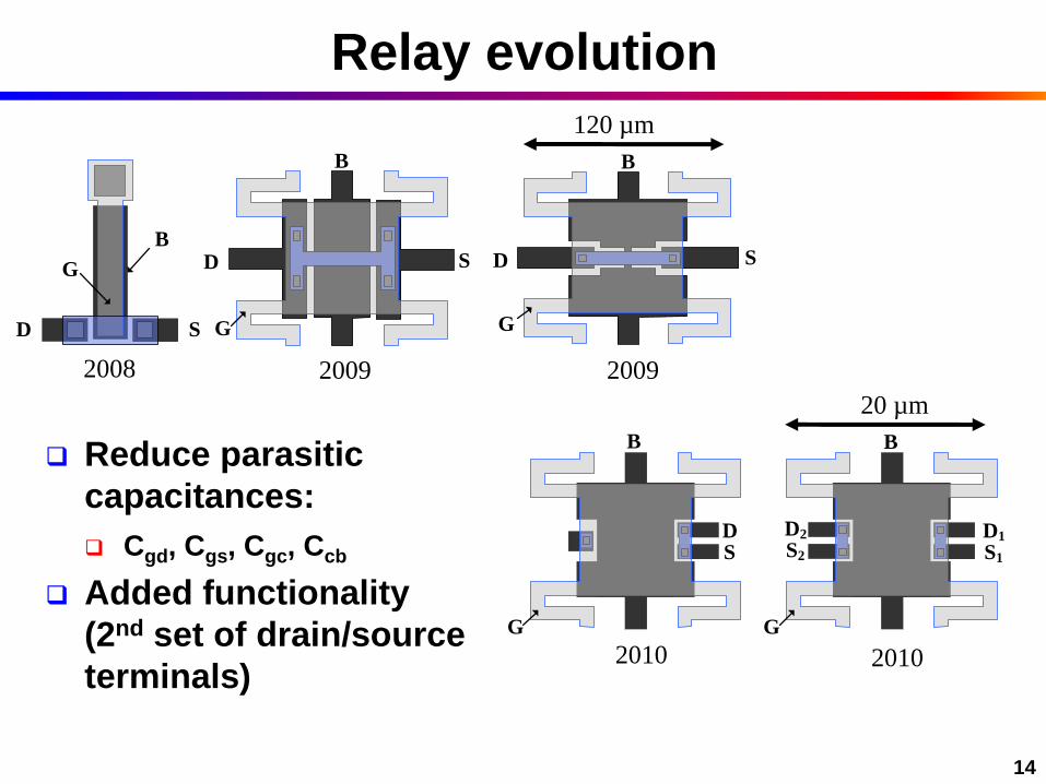
Relay evolution
Reduce parasitic
capacitances:
Cgd, Cgs, Cgc, Ccb
Added functionality
(2nd set of drain/source
terminals)
G
D S
B
G
D S
B
D S
G
B
D1
S1
G
D2
S2
BB
DS
G
20 µm
120 µm
2008 2009 2009
2010 2010

15
6T Relay ~Halves the device count
Adder: ½ the number of devices in the PGK
Same gains in all logic functions
A
B
CinA
Cin
A
B
Vdd
A
B
A
B
Cout
kill
generate
propagate
Vdd
A
B
A
B
Cout
generate
kill
propagate
B
A
Vdd
Vdd
S
A
B
Cin
A
Cin
A
B
Cout
kill
pro
pa
ga
te
Cout
gen
era
te
BS
A
Vdd
Vdd
A
BVdd

16
Towards more complex designs: Multiplier
x
+
Partial products
Multiplicand
Multiplier
Result
1 0 1 0 1 0
1 0 1 0 1 0
1 0 1 0 1 0
1 1 1 0 0 1 1 1 0
0 0 0 0 0 0
1 0 1 0 1 0
1 0 1 1
2 possible scenarios
Using full- and half-adders along the columns
Using bigger compressors along the columns to achieve higher compression
Design tradeoff: Number of stages (i.e., mechanical delays) vs. area Example: 32 bit relay multiplier CMOS style design: 19 mech. delay, 26k relays
Optimized Relay design: 5-6 mech. delay, 11k-20k relays
Multiplier
Multiplicand
Partial Products
(PP)
Result
17
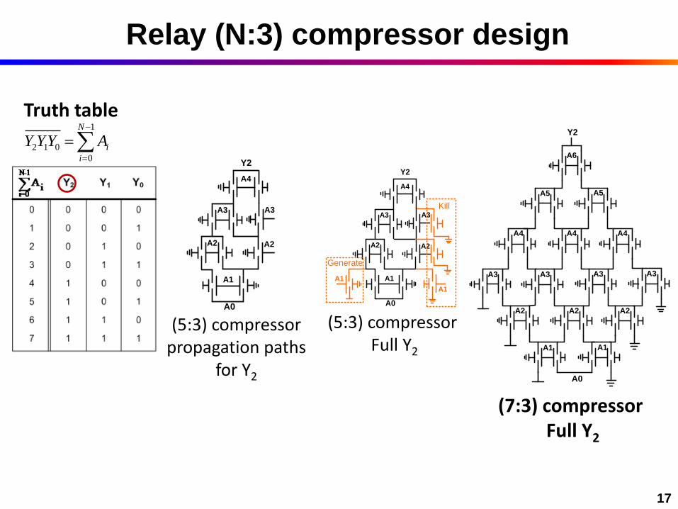
Truth table 1
2 1 0
0
N
i
i
Y YY A
A0
A1
A2
A3
A2
A4
A3
Y2
A1
(5:3) compressor propagation paths
for Y2
(5:3) compressor Full Y2
Y2
A0
A1
A2
A3
A4
A5
A6
A1
A2 A2
A3A3A3
A4A4
A5
(7:3) compressor Full Y2
Relay (N:3) compressor design
Generate
A0
A1
A2
A3
A2
A4
A3
Y2
A1
A1
Kill

18
(7:3) Relay compressor measurements
Largest working MEM-Relay circuit reported to date (98 relays)
0 20 40 60 80 100 120
1
3
5
7
Input code
Ou
tpu
t c
od
e Correct resultExperiment
(7:3) compressor input vs. output code
0
2
4
Y0
(V) 0
2
4
Y1 (V
) 0
2
4
Y2
(V)
0 0.5 1 1.5 2 2.5 3 3.5 40
50
100
Inp
ut
co
de
Time (S)
(7:3) compressor sub-circuits output
A0 A0
Y1
A1A1A1A1
A2A2A2A2
A3A3A3 A3
A4A4A4
A5A5
A6
A0
A0
Y0 Y0
A1
A2
A3
A4
A5
A6
A1
A2
A3
A4
A5
A6
Y2
A0
A1
A2
A3
A4
A5
A6
A1
A2 A2
A3A3A3
A4A4
A5
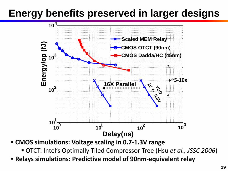
19
100
101
102
10310
1
102
103
104
Delay(ns)
En
erg
y/o
p (
fJ)
Scaled MEM Relay
CMOS OTCT (90nm)
CMOS Dadda/HC (45nm)
16X Parallel VD
D
1V
ß 0
.5V
Energy benefits preserved in larger designs
CMOS simulations: Voltage scaling in 0.7-1.3V range OTCT: Intel’s Optimally Tiled Compressor Tree (Hsu et al., JSSC 2006)
Relays simulations: Predictive model of 90nm-equivalent relay
~5-10x
20
Toward full systems - Relay scaling
1um litho
Scaled Relay size
20um x 20um
Sematech
Relay size
120um x 150um
0.25um litho

21
Conclusions
MEM relays offer a lower minimum E/op than CMOS
Reliability of MEM relays improving
Demonstrated simple circuits
Can start to think about building more complex systems
CLICKR Platform designed for multiple foundries
and devices
Energy-gains preserved for larger blocks
Designs moving toward scaled devices and full VLSI
systems
22
Graduate students
Fred Chen, Hossein Fariborzi
Cheng Wang, Kevin Dwan, Mingzhe Jiang
Matthew Spencer, Abhinav Gupta, Patrick Kwong
Hei Kam, Rhesa Nathanael, Vincent Pott, Jaeseok Jeon
Sponsors
DARPA NEMS program
FCRP (C2S2, MSD)
MIT CICS, Berkeley Wireless Research Center, UCLA ICSL
NSF
Acknowledgments
23
Experimental Relay Circuits: Inverter
Circuit Diagram Voltage Waveforms Voltage Transfer Char.

24
MEM Relay Multiplier: 6-bit Example
Approach 1: Full- and Half-adders 3 mech. delay
Approach 2: Large compressors 2 mech. delay
Partial Product Generation matrix
MultiplierMultiplicand
LSB
12-bit Multiplication result
5LSB
67654
12-bit Multiplication result
Partial Product Generation matrix
Elec. Propagation
Mech. Propagation
N
(N:3)
Compressor
FA
HA
Mech.
delay

25
(7:3) Compressor: CMOS vs. Relay
A0
Y2
A0
A1
A2
A3
A4
A5
A6
A1
A1
A1
A2A2A2
A2
A2
A3A3
A3
A3 A3 A3A3
A4A4A4A4
A4
A5 A5
A5
A6
Y2
(7:3) compressor Full Y2, CMOS(1)
(1) Song et al, JSCC 91
Truth table 1
2 1 0
0
N
i
i
Y YY A
Y2
A0
A1
A2
A3
A4
A5
A6
A1
A2 A2
A3A3A3
A4A4
A5
(7:3) compressor Full Y2,relays
Relay implementation of CMOS pass-gate compressor: No propagation path accumulating mech. delays in stages 19 mech. delay for a 32 bit multiplier
Optimized relay design: zero mech. delay from A0 to Y2
5 mech. delay for a 32 bit multiplier