Embed Size (px)
Citation preview
1A Bipolar Linear Regulator
LR1117C
DESCRIPTION
LR1117C is a series of low dropout three- terminal regulators with a dropout of 1.3V at 1A load current. LR1117C features a very low standby current 2mA compared to 5mA of competitor. Other than a fixed version, Vout = 1.2V, 1.5V, 1.8V, 2.5V, 3.3V, 5V, and 12V, LR1117C has an adjustable version, which can provide an output voltage from 1.25 to 12V with only two external resistors. LR1117C offers thermal shut down and current limit functions, to assure the stability of chip and power system. And it uses trimming technique to
guarantee output voltage accuracy within 2%. Other output voltage accuracy can be customized
on demand, such as 1% LR1117C is available in SOT-223, TO-252 power package.
FEATURES
Other than a fixed version and an adjustable version, output value can be customized on demand.
Maximum output current is 1A
Range of operation input voltage: Max 12V
Standby current: 2mA (typ.)
Line regulation: 0.1%/V (typ.)
Load regulation: 10mV (typ.)
Environment Temperature: -40C~85C
APPLICATIONS
Power Management for Computer Mother Board, Graphic Card
BLD Monitor and BLD TV
DVD Decode Board
ADSL Modem
Post Regulators for Switching Supplies
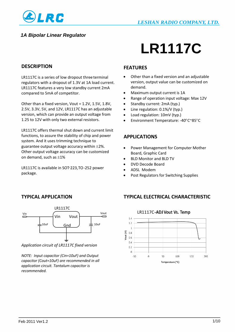
TYPICAL APPLICATION
Vin Vout
Gnd10uF 10uF
Vin Vout
LR1117C
Application circuit of LR1117C fixed version NOTE: Input capacitor (Cin=10uF) and Output capacitor (Cout=10uF) are recommended in all application circuit. Tantalum capacitor is recommended.
TYPICAL ELECTRICAL CHARACTERISTIC
LR111 7C
LESHAN RADIO COMPANY, LTD.
Feb 2011 Ver1.2 1/10
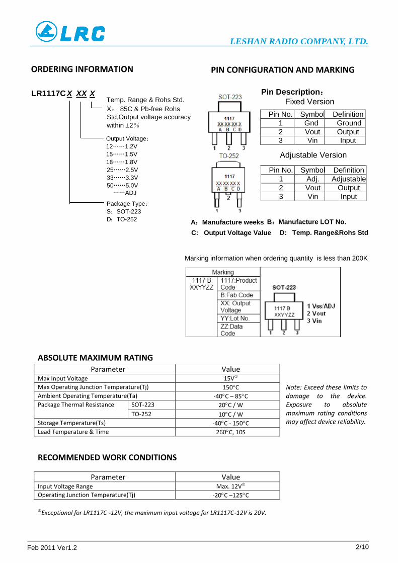
ORDERING INFORMATION
LR1117C XX X X
ABSOLUTE MAXIMUM RATING
PIN CONFIGURATION AND MARKING
Pin Description: Fixed Version
Adjustable Version
Note: Exceed these limits to damage to the device. Exposure to absolute maximum rating conditions may affect device reliability.
RECOMMENDED WORK CONDITIONS
Parameter Value Input Voltage Range Max. 12V
Operating Junction Temperature(Tj) -20C –125C
Exceptional for LR1117C -12V, the maximum input voltage for LR1117C-12V is 20V.
Pin No. Symbol Definition
1 Gnd Ground
2 Vout Output 3 Vin Input
Pin No. Symbol Definition
1 Adj. Adjustable
2 Vout Output
3 Vin Input
Parameter Value Max Input Voltage 15V
Max Operating Junction Temperature(Tj) 150C
Ambient Operating Temperature(Ta) -40C – 85C
Package Thermal Resistance SOT-223 20C / W
TO-252 10C / W
Storage Temperature(Ts) -40C - 150C
Lead Temperature & Time 260C, 10S
Package Type:
S:SOT-223
D:TO-252
Temp. Range & Rohs Std.
X: 85C & Pb-free Rohs
Std,Output voltage accuracy
within 2% Output Voltage:
12……1.2V
15……1.5V
18……1.8V
25……2.5V
33……3.3V
50……5.0V
A:Manufacture weeks
B:Manufacture LOT No. C: Output Voltage Value
D: Temp. Range&Rohs Std
……ADJ
LESHAN RADIO COMPANY, LTD.
Feb 2011 Ver1.2 2/10
Marking information when ordering quantity is less than 200K
ELECTRICAL CHARACTERISTICS Tj=25C
Symbol Parameter Conditions Min Typ Max Unit
Vref Reference Voltage LR1117-ADJ
1.225 1.25 1.275 V 10mA≤Iout≤1A , Vin=3.25V
Vout Output Voltage
LR1117-1.2V 1.176 1.2 1.224 V
0≤Iout≤1A , Vin=3.2V
LR1117-1.5V 0≤Iout≤1A , Vin=3.5V
1.47 1.5 1.53 V
LR1117-1.8V 1.764 1.8 1.836 V
0≤Iout≤1A , Vin=3.8V
LR1117-2.5V 2.45 2.5 2.55 V
0≤Iout≤1A , Vin=4.5V
LR1117-3.3V 3.234 3.3 3.366 V
0≤Iout≤1A , Vin=5.3V
LR1117-5.0V 4.9 5 5.1 V
0≤Iout≤1A , Vin=7.0V
LR1117-12.0V 11.76 12 12.24 V
0≤Iout≤1A , Vin=14V
ΔVout Line Regulation
LR1117-1.2V 0.1 0.2 %/V
Iout=10mA, 2.7V≤Vin≤10V
LR1117-ADJ 0.1 0.2 %/V
Iout=10mA, 2.75V≤Vin≤12V
LR1117-1.5V
out=10mA, 3.0V≤Vin≤12V 0.1 0.2 %/V
LR1117-1.8V
Iout=10mA, 3.3V≤Vin≤12V
LR1117-2.5V 0.1 0.2 %/V
Iout=10mA, 4.0V≤Vin≤12V
LR1117-3.3V 0.1 0.2 %/V
Iout=10mA, 4.8V≤Vin≤12V
LR1117-5.0V 0.1 0.2 %/V
Iout=10mA, 6.5V≤Vin≤12V
LR1117-12.0V 0.1 0.2 %/V
Iout=10mA, 13.5V≤Vin≤20V
ΔVout Load Regulation
LR1117-1.2V 10 30 mV
Vin =2.7V, 10mA≤Iout≤1A
LR1117-ADJ 10 30 mV
Vin =2.75V, 10mA≤Iout≤1A
LR1117-1.5V
Vin=3.0V, 10mA≤Iout≤1A 10 30 mV
LR1117-1.8V
Vin=3.3V, 10mA≤Iout≤1A
LR1117-2.5V 10 30 mV
Vin=4.0V, 10mA≤Iout≤1A
LR1117-3.3V 10 30 mV
Vin=4.8V, 10mA≤Iout≤1A
LR1117-5.0V 10 30 mV
Vin=6.5V, 10mA≤Iout≤1A
LR1117-12.0V 10 30 mV
Vin=13.5V, 10mA≤Iout≤1A
LESHAN RADIO COMPANY, LTD.
Feb 2011 Ver1.2 3/10
ELECTRICAL CHARACTERISTICS continued
Tj=25C
Symbol Parameter Conditions Min Typ Max Unit
Vdrop Dropout Voltage Iout=100mA 1.23 1.3 V
Iout=1A 1.3 1.5 V
Ilimit Current Limit Vin-Vout=2V, Tj=25°C 1 A
SVR Supply Voltage Rejection f = 120Hz, VIN − VOUT = 3V + 1VPP Ripple
60
dB
Imin Minimum Load Current LR1117-ADJ 2 10 mA
Iq Quiescent Current
LR1117-1.2V, Vin =10V 2 5 mA
LR1117-1.5V, Vin =11V 2 5 mA
LR1117-1.8V, Vin =12V 2 5 mA
LR1117-2.5V,Vin =12V 2 5 mA
LR1117-3.3V, Vin =12V 2 5 mA
LR1117-5.0V, Vin =12V 2 5 mA
LR1117-12.0V, Vin =20V 2 5 mA
IAdj Adjust Pin Current LR1117-ADJ
55 120 uA Vin =5V, 10mA≤Iout≤1A
Ichange Iadj change LR1117-ADJ
0.2 10 uA Vin =5V, 10mA≤Iout≤1A
ΔV/ΔT Temperature coefficient ±100 ppm
JC Thermal Resistance
SOT-223 20
°C/W TO-252 10
JA
Thermal Resistance Junction-to-Ambient (No air flow)
SOT-223 (No heat sink) 136 °C/W
TO-252 (No heat sink) 92
Note1: All test are conducted under ambient temperature 25°C and within a short period of time 20ms Note2: Load current smaller than minimum load current of LR1117C-ADJ will lead to unstable or oscillation output.
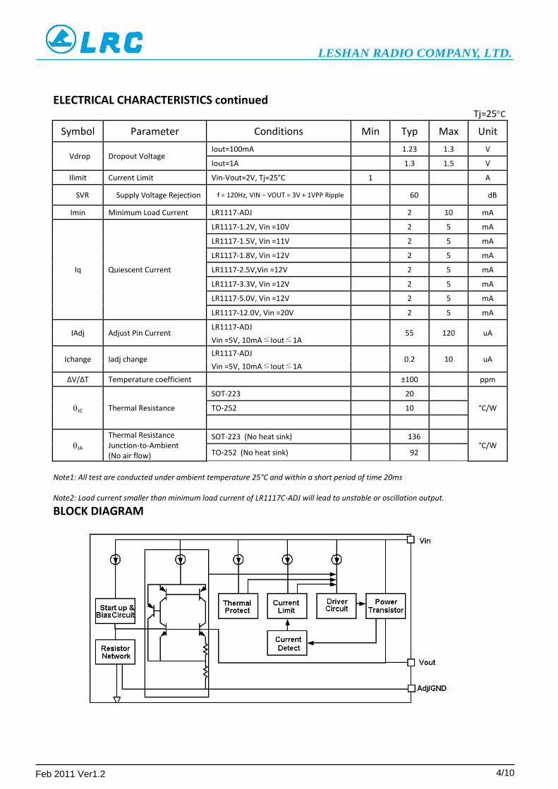
BLOCK DIAGRAM
LESHAN RADIO COMPANY, LTD.
Feb 2011 Ver1.2 4/10
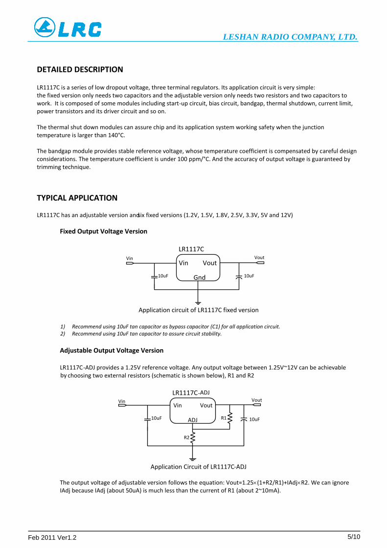
DETAILED DESCRIPTION LR1117C is a series of low dropout voltage, three terminal regulators. Its application circuit is very simple: the fixed version only needs two capacitors and the adjustable version only needs two resistors and two capacitors to work. It is composed of some modules including start-up circuit, bias circuit, bandgap, thermal shutdown, current limit, power transistors and its driver circuit and so on. The thermal shut down modules can assure chip and its application system working safety when the junction temperature is larger than 140°C. The bandgap module provides stable reference voltage, whose temperature coefficient is compensated by careful design considerations. The temperature coefficient is under 100 ppm/°C. And the accuracy of output voltage is guaranteed by trimming technique.
TYPICAL APPLICATION LR1117C has an adjustable version and six fixed versions (1.2V, 1.5V, 1.8V, 2.5V, 3.3V, 5V and 12V)
Fixed Output Voltage Version
Vin Vout
Gnd10uF 10uF
Vin Vout
LR1117C
Application circuit of LR1117C fixed version
1) Recommend using 10uF tan capacitor as bypass capacitor (C1) for all application circuit. 2) Recommend using 10uF tan capacitor to assure circuit stability.
Adjustable Output Voltage Version
LR1117C-ADJ provides a 1.25V reference voltage. Any output voltage between 1.25V~12V can be achievable by choosing two external resistors (schematic is shown below), R1 and R2
Vin Vout
ADJ10uF 10uF
Vin Vout-ADJ
R1
R2
Application Circuit of LR1117C-ADJ
The output voltage of adjustable version follows the equation: Vout=1.25(1+R2/R1)+IAdjR2. We can ignore IAdj because IAdj (about 50uA) is much less than the current of R1 (about 2~10mA).
LR1117C
LESHAN RADIO COMPANY, LTD.
Feb 2011 Ver1.2 5/10
1) To meet the minimum load current (>10mA) requirement, R1 is recommended to be 125ohm or lower. As LR1117C-ADJ
can keep itself stable at load current about 2mA, R1 is not allowed to be higher than 625ohm.
2) Using a bypass capacitor (CADJ) between the ADJ pin and ground can improve ripple rejection. This bypass capacitor prevents ripple from being amplified as the output voltage is increased. The impedance of CADJ should be less than R1 to prevent ripple from being amplified. As R1 is normally in the range of 100Ω~500Ω, the value of CADJ should satisfy
this equation: 1/(2frippleCADJ)<R1.
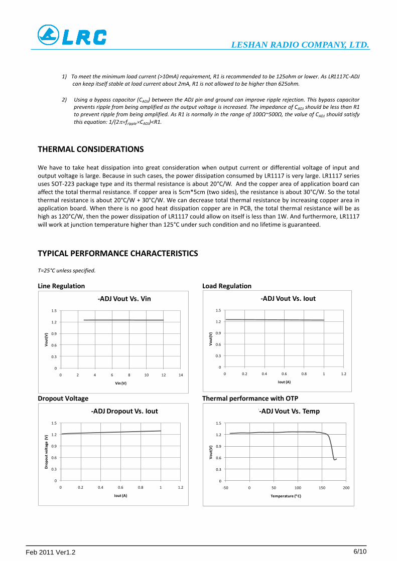
THERMAL CONSIDERATIONS We have to take heat dissipation into great consideration when output current or differential voltage of input and output voltage is large. Because in such cases, the power dissipation consumed by LR1117 is very large. LR1117 series uses SOT-223 package type and its thermal resistance is about 20°C/W. And the copper area of application board can affect the total thermal resistance. If copper area is 5cm*5cm (two sides), the resistance is about 30°C/W. So the total thermal resistance is about 20°C/W + 30°C/W. We can decrease total thermal resistance by increasing copper area in application board. When there is no good heat dissipation copper are in PCB, the total thermal resistance will be as high as 120°C/W, then the power dissipation of LR1117 could allow on itself is less than 1W. And furthermore, LR1117 will work at junction temperature higher than 125°C under such condition and no lifetime is guaranteed.
TYPICAL PERFORMANCE CHARACTERISTICS T=25°C unless specified.
Line Regulation Load Regulation
0
0.3
0.6
0.9
1.2
1.5
0 2 4 6 8 10 12 14
Vo
ut(
V)
Vin (V)
LC1117-ADJ Vout Vs. Vin
0
0.3
0.6
0.9
1.2
1.5
0 0.2 0.4 0.6 0.8 1 1.2
Vo
ut(
V)
Iout (A)
LC1117-ADJ Vout Vs. Iout
Dropout Voltage Thermal performance with OTP
0
0.3
0.6
0.9
1.2
1.5
0 0.2 0.4 0.6 0.8 1 1.2
Dro
po
ut
volt
age
(V
)
Iout (A)
LC1117-ADJ Dropout Vs. Iout
0
0.3
0.6
0.9
1.2
1.5
-50 0 50 100 150 200
Vo
ut(
V)
Temperature (C)
LC1117-ADJ Vout Vs. Temp
LESHAN RADIO COMPANY, LTD.
Feb 2011 Ver1.2 6/10
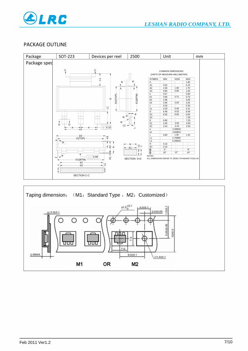
PACKAGE OUTLINE
Package SOT-223 Devices per reel 2500 Unit mm
Package specification:
ee1
e
E
L1
L1
θ
θ
L
L2
C C
D D
c1 c
b1
b
SECTION D-D
θ
b2
c1c b3
SECTION C-C
6.536.48 6.58D
θ 0° - 8°
R1 0.10 - -
L1 1.75REF
1.201.000.80L
e 2.30BSC
-6.80 7.20E
c1 0.310.29 0.30
-0.30 0.35c
b1 0.760.66 0.71
-0.67 0.80b
A3 1.000.80 0.90
1.60
-
-
1.50 1.70A2
A1 0.100.02
- 1.80A
MAXNOMMINSYMBOL
(UNITS OF MEASURE=MILLIMETER)
COMMON DIMENSIONS
3.40 3.50 3.60E1
e1 4.60BSC
L2 0.25BSC
R -0.10 -
θ 14°12°10°
D(TOP)
θ
A3
A2
A
A1
R
R
b3 3.052.95 3.00
-2.96 3.09b2
ALL DIMENSIONS REFER TO JEDEC STANDARD TO261-AA
NOTES:
E1
(BT
M)
E2
(TO
P)
D1(BTM)
θ
6.606.55 6.65D1
3.33 3.43 3.53E20.10
0.08
D2
-- 7.05D2
Taping dimension:(M1:Standard Type ,M2:Customized)
LESHAN RADIO COMPANY, LTD.
Feb 2011 Ver1.2 7/10
Taping reel dimension:
Package TO-252 Devices per reel 2500 Unit mm
Package specification:
LESHAN RADIO COMPANY, LTD.
Feb 2011 Ver1.2 8/10
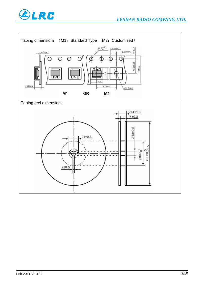
Taping dimension:(M1:Standard Type ,M2:Customized)
Taping reel dimension:
LESHAN RADIO COMPANY, LTD.
Feb 2011 Ver1.2 9/10
Disclaimer
The product information and the selection guides facilitate the selection of LRC's best suited devices for application in your product(s) as per your requirement. It is recommended that you completely review our Data Sheet(s) so as to confirm that the Device(s) meet the performance parameters for your application. The information furnished on LRC’s Website, due to the constraint of time and certain conditions, may not be updated timely and is only for customer’s reference. Therefore, LRC does not assume responsibility arising from inaccuracies or incomplete information. If necessary, customer is requested to contact LRC’s service support for confirmation and accurate information. Furthermore, LRC does not assume liability whatsoever, arising out of the improper application or use of any LRC product; neither does it convey any license under its patent rights nor rights of other intellectual properties. LRC strives for continuous improvement and reserves the right to change the specifications of its products without prior notice.
No. 287 West People Road, Leshan, Sichuan, China. Telephone: + 86-833-2150227 Fax: + 86-833-2150003
E-mail: [email protected] Website: www.lrc.cn
LESHAN RADIO COMPANY, LTD.
Feb 2011 Ver1.2 10/10