Embed Size (px)
Citation preview

89TSF552Preliminary Information*
Switch Fabric Data Sheet
DescriptionThe 89TSF5xx is a complete switch fabric, consisting of two chips:
89TSF552 (queuing engine, 10 Gbps).89TSF500 (crossbar and scheduler).
The 89TSF552 typically resides on a line card and the 89TSF500usually resides on a separate switch card. An 89TSF552 connects withthe 89TSF500 through high-speed serial links.
The 89TSF5xx switch fabric has a modular and scalable architecturethat gives system designers maximum flexibility and performance. Thisarchitecture allows a switch to be implemented either on a single shelfusing an electrical backplane or on multiple shelves connected byoptical transceivers, thus helping system vendors overcome physicalspace constraints.
The 89TSF552 supports line card speeds up to OC-192 (full duplex).It incorporates a 16-bit CSIX-over-LVDS interface to line card devices,allowing the 89TSF5xx to operate seamlessly with the IDT 89TTM552traffic manager, or other compatible traffic managers and networkprocessors.
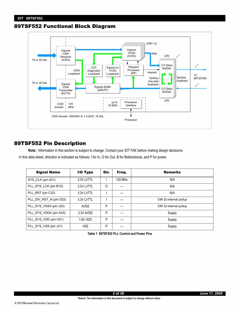
In the ingress direction, the 89TSF552 manages a set of virtualoutput queues (VOQs), negotiates the routing path through the switchfabric, and transmits data to an 89TSF500. In the egress direction, the89TSF552 receives data from an 89TSF500 and transmits the traffic,through a CSIX-over-LVDS interface, either to IDT’s 89TTM552 trafficmanager or to another device (such as a network processor) on the linecard.
89TSF5xx Features Up to 32 switch ports, with 24 Gbps available per switch
port. Variable length CSIX payload (up to 132 bytes) that supports
any type of traffic. Virtual output queues (VOQs) in the ingress direction that
eliminate head-of-line blocking. The 256 unicast VOQsprovide:
– A maximum of 32 ports with 8 CoS, or– A maximum of 16 ports with 4 subports and 4 CoS.
Spatial multicast support with up to 4K global multicastlabels. Each multicast label can specify from 1 to 32 ports.
Efficient backpressure mechanism that eliminates cell losscaused by congestion.
In-service scalable architecture. “Stackable” architecture. Total aggregate bandwidth is
linearly proportional to the number of 89TSF500s. Port rate
1 of © 2005 Integrated Device Technology, Inc. *Notice: The information in this docume
IDT and the IDT logo are trademarks of Int
is configurable up to OC-192. Always non-blocking architecture across destination, traffic
type (cell, packet), and class of service (CoS). Supports up to 4 egress subports per switch port. Carrier class reliability features:
– Flexible architecture that allows the 89TSF switch fabric to beemployed in a single switch shelf or in multiple switch shelves.
– Automatic link diagnostics that detect faulty link connections.– Both n+m (load-sharing mode) and 1:1 protection (active/
standby mode) on serial links.– Patented error correction scheme to reduce the system bit
error rate by 105.– Line cord redundancy via Redundant Destination Mapping
(RDM) and Queue-Mapped Redundancy (QMR).– Dynamic 89TSF500 rerouting that avoids congested or faulty
89TSF500s.– Zero cell loss during controlled switchover to standby
89TSF500s. Advanced diagnostic features including multiple loopback
paths. Unicast and multicast traffic with up to 8 classes of service. Industry-standard CSIX-over-LVDS interface. Backward compatibility with IDT’s ZSF200 switch fabric.
89TSF552 Features 24 embedded SerDes links per device at 2.5 Gbps per link. Virtual output queues (VOQs) that buffer data according to
destination, traffic type and class of Service (CoS). Guaranteed cell ordering. External processor interface for status and register
configuration. Support for n+m (load-sharing) and 1:1 (active/standby)
redundancy modes.
38 June 17, 2005nt is subject to change without notice DSC 6799
egrated Device Technology, Inc.
IDT 89TSF552
89TSF552 Functional Block Diagram
89TSF552 Pin DescriptionNote: Information in this section is subject to change. Contact your IDT FAE before making design decisions.
In this data sheet, direction is indicated as follows: I for In, O for Out, B for Bidirectional, and P for power.
Signal Name I/O Type Dir. Freq. Remarks
SYS_CLK (pin A21) 3.3V LVTTL I 125 MHz N/A
PLL_SYS_LCK (pin B19) 3.3V LVTTL O — N/A
PLL_RST (pin C22) 3.3V LVTTL I — N/A
PLL_DIV_RST_N (pin D22) 3.3V LVTTL I — 33K Ω internal pullup
PLL_SYS_VSSA (pin J20) AVSS P — 33K Ω internal pullup
PLL_SYS_VDDA (pin K20) 3.3V AVDD P — Supply
PLL_SYS_VDD (pin H21) 1.8V VDD P — Supply
PLL_SYS_VSS (pin J21) VSS P — Supply
Table 1 89TSF552 PLL Control and Power Pins
data
2.5 GbpsSerDes
Ingress CSIX
Receiver (ICRX)
Egress CSIX
Transmitter(ECTX)
Ingress VOQs(IVOQ)
request
Request Processor
(RP)
C2C DiagnosticLoopback
2.5 GbpsSerDes
Egress Buffer (EBUFF)
Processor Interface
Processor
up to33 MHz125
MHzCSIX
domain
(24)
(24)
• • •
(256 + 2)
To 89TSF500
• • •
• • •
CSIXLoopback
CSIX domain: 500 MHz to 1.0 GHZ, 16 bits.
16 or 32 bits
16 or 32 bits
Egress to IVOQ
LoopbackSerDes
line-sideloopback
SerDes loopback
2 of 38 June 17, 2005*Notice: The information in this document is subject to change without notice

IDT 89TSF552
Signal Name I/O Type Dir. Freq. Remarks
SD[2:0]_REFCLKN (pins A25, Y39, AW26)
Serdes diff clock I 250MHz Reference clocks for both Rx and Tx.The reference clock (SD[n]_REFCLKN and SD[n]_REFCLKP) must be synchronous to twice the sys-tem clock (SYS_CLK) input.If an entire SerDes group is not used, the reference clock pins for that group should be pulled down to VSS using a 300Ω to 1kΩ resistor.
SD[2:0]_REFCLKP(pins A26, AA39, AW25)
Serdes diff clock I 250MHz
SD[2:0]_REF_RES(pins D26, AA36, AT25)
Serdes Bidi O — Reference resistor pins used to generate bias currents for both Rx and Tx.To ensure proper biasing, connect each of these to VSS through a 3.09 kΩ 1% resistor.If an entire SerDes group is not used, the reference resistor pins for that group should be connected to VDD_SD (1.8V).
VDD_SD[2:0]_PLL (pins J23, Y31, AL24)
VAA18 P — SerDes common VDD = 1.8V. These are PLL analog power inputs and should be well filtered.
VSS_SD[2:0]_PLL (pins K22, W31, AL23)
VSS P — SerDes PLL ground
VDD_REFCLK[2:0](pins J24, AA31, AK22)
VAA33 P — SerDes common VDD = 3.3V
RXN[23:0] Serdes diff input I — SerDes Rx differential pairs. A link should be left open (n.c.) if it is not used
RXP[23:0] Serdes diff input I —
TXN[23:0] Serdes diff output O — SerDes Tx differential pairs. A link should be left open (n.c.) if it is not used
TXP[23:0] Serdes diff output O —
VDD_SD VAA18 P — SerDes VDD (1.8V)
VDD_TX VAA25 P — SerDes VDD (2.5V)
VSS VSS P — Serdes ground included in Table 8 (89TSF552 Misc. Pins)
Table 2 89TSF552 SerDes Pins
Signal Name Type Dir. Freq. Remarks
ZBUS_AVALID_N (pin AR11) 3.3V LVTTL I 33MHz 33K Ω internal pullup
ZBUS_CLK (pin AW7) 3.3V LVTTL I 33MHz N/A
ZBUS_AD[15:0] 3.3V LVTTL B 33MHz 33K Ω internal pullup
ZBUS_DEVID[4:0] 3.3V LVTTL I — 33K Ω internal pullup
ZBUS_DVALID_N (pin AV10) 3.3V LVTTL B 33MHz 33K Ω internal pullup
ZBUS_INT_N[2:0](pins AW11, AV11, AU11)
3.3V LVTTL O — 33K Ω internal pullup
ZBUS_PRTY (pin AV9) 3.3V LVTTL B 33MHz 33K Ω internal pullup
Table 3 89TSF552 ZBus Pins
3 of 38 June 17, 2005*Notice: The information in this document is subject to change without notice

IDT 89TSF552
Signal Name I/O Type Dir. Freq. Remarks
TCK (pin E19) 3.3V LVTTL I — 33K internal pullup
TDI (pin F19) 3.3V LVTTL I — 33K internal pullup
TDO (pin C18) 3.3V LVTTL O — 33K internal pullup
TMS (pin D19) 3.3V LVTTL I — 33K internal pullup
TRST_N (pin C19) 3.3V LVTTL I — 33K internal pullup
Table 4 89TSF552 Test and Debugging Pins
Signal Name I/O Type Dir. Freq. Remarks
ZTICK (pin AU12) 3.3V LVTTL I — External reference ZTick input to which the internal ZTick logic will synchronize. If ZTICK_MODE is 0, ZTICK can be left open.
ZTICK_MODE (pin AP16) 3.3V LVTTL I — External ZTick select. (Enable external ZTick sync.)1 = internal ZTick to be synchronized to ext. reference ZTick0 = internal ZTick is async to any ext. ZTick.Pin(s) must be stable at least 16 ns before the deassertion of the RESET_N input. Any change in pin(s) after 16 ns before the deassertion of the RESET_N input must be concurrent with, or followed by, an assertion of the RESET_N input.
Table 5 89TSF552 ZTick Management Pins
Signal Name I/O Type Dir. Freq. Remarks
CRX_REFCLK (pin AH1) 3.3V LVTTL I 75-125MHz CSIX Rx reference clock. This reference clock controls the bit rate on the CRX control bus outputs.PLL_CRX_RST (pin AH5) 3.3V LVTTL I —
PLL_CRX_LCK (pin AH6) 3.3V LVTTL O —
PLL_CRX_VDD (pin AD9) 1.8V AVDD P — Digital power (1.8V)
PLL_CRX_VDDA (pin AC9) 3.3V AVDD P — Analog power (3.3V)
PLL_CRX_VSS (pin AD10) VSS P — Digital ground
PLL_CRX_VSSA (pin AC10) AVSS P — Analog ground
CTX_REFCLK (pin F1) 3.3V LVTTL I 75-125MHz CSIX Tx reference clock. This reference clock controls the bit rate on the CTX data bus outputs.PLL_CTX_RST (pin G3) 3.3V LVTTL I —
PLL_CTX_LCK (pin G4) 3.3V LVTTL O —
PLL_CTX_VDD (pin U9) 1.8V AVDD P — Digital power (1.8V)
PLL_CTX_VDDA (pin T9) 3.3V AVDD P — Analog power (3.3V)
PLL_CTX_VSS (pin U10) VSS P — Digital ground
PLL_CTX_VSSA (pin T10) AVSS P — Analog ground
Table 6 89TSF552 CSIX PLL Pins
4 of 38 June 17, 2005*Notice: The information in this document is subject to change without notice
IDT 89TSF552
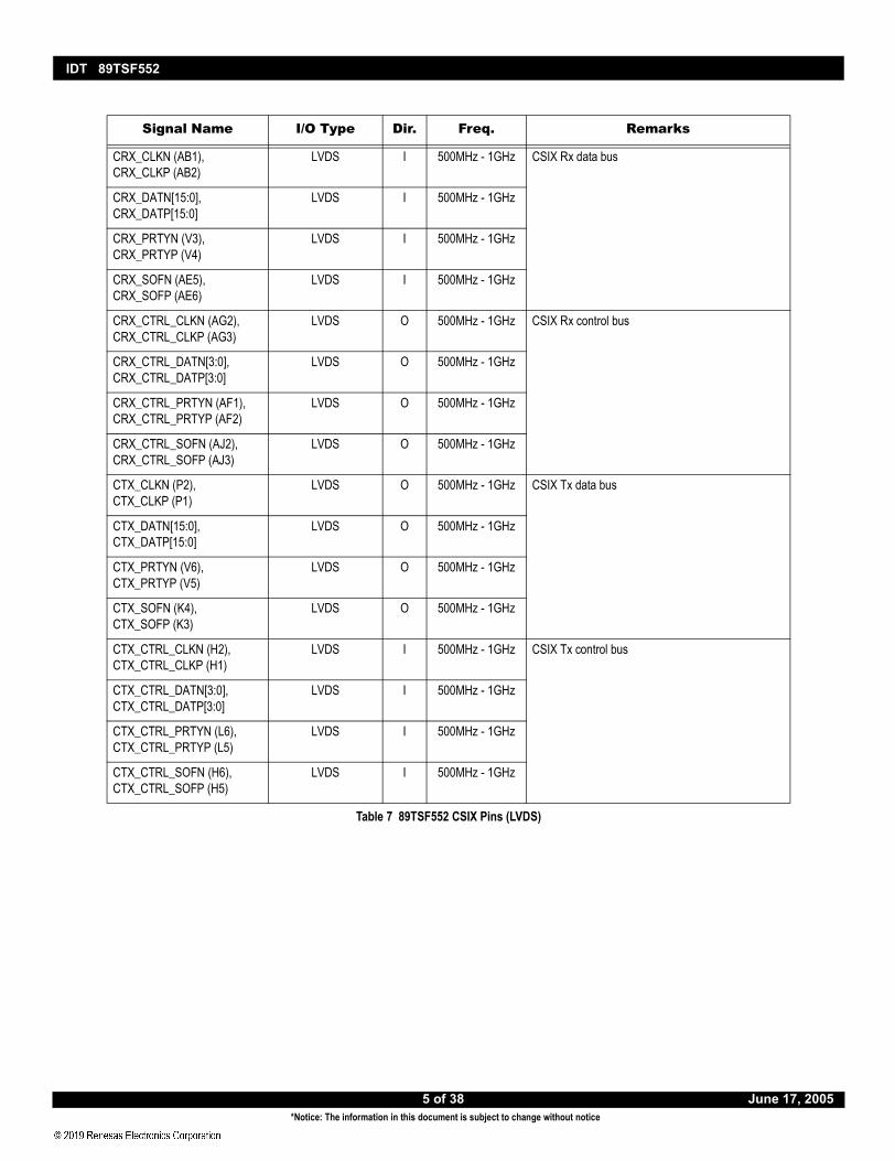
Signal Name I/O Type Dir. Freq. Remarks
CRX_CLKN (AB1), CRX_CLKP (AB2)
LVDS I 500MHz - 1GHz CSIX Rx data bus
CRX_DATN[15:0], CRX_DATP[15:0]
LVDS I 500MHz - 1GHz
CRX_PRTYN (V3), CRX_PRTYP (V4)
LVDS I 500MHz - 1GHz
CRX_SOFN (AE5), CRX_SOFP (AE6)
LVDS I 500MHz - 1GHz
CRX_CTRL_CLKN (AG2), CRX_CTRL_CLKP (AG3)
LVDS O 500MHz - 1GHz CSIX Rx control bus
CRX_CTRL_DATN[3:0], CRX_CTRL_DATP[3:0]
LVDS O 500MHz - 1GHz
CRX_CTRL_PRTYN (AF1), CRX_CTRL_PRTYP (AF2)
LVDS O 500MHz - 1GHz
CRX_CTRL_SOFN (AJ2), CRX_CTRL_SOFP (AJ3)
LVDS O 500MHz - 1GHz
CTX_CLKN (P2), CTX_CLKP (P1)
LVDS O 500MHz - 1GHz CSIX Tx data bus
CTX_DATN[15:0], CTX_DATP[15:0]
LVDS O 500MHz - 1GHz
CTX_PRTYN (V6), CTX_PRTYP (V5)
LVDS O 500MHz - 1GHz
CTX_SOFN (K4), CTX_SOFP (K3)
LVDS O 500MHz - 1GHz
CTX_CTRL_CLKN (H2), CTX_CTRL_CLKP (H1)
LVDS I 500MHz - 1GHz CSIX Tx control bus
CTX_CTRL_DATN[3:0], CTX_CTRL_DATP[3:0]
LVDS I 500MHz - 1GHz
CTX_CTRL_PRTYN (L6), CTX_CTRL_PRTYP (L5)
LVDS I 500MHz - 1GHz
CTX_CTRL_SOFN (H6), CTX_CTRL_SOFP (H5)
LVDS I 500MHz - 1GHz
Table 7 89TSF552 CSIX Pins (LVDS)
5 of 38 June 17, 2005*Notice: The information in this document is subject to change without notice

IDT 89TSF552
89TSF552 Electrical and Timing CharacteristicsSome data are TBD and will be published as they become available. The specifications are subject to change without notice.
89TSF552 Absolute Maximum RatingsThe absolute maximum ratings are the maximum conditions that the device can withstand without sustaining permanent damage. Exceeding any
of these conditions could result in permanent damage to the device. Normal operation should not be expected at these conditions. In addition, expo-sure to absolute maximum rated conditions (or near absolute maximum rated conditions) for extended periods may affect device reliability.
Operation of the device is not guaranteed at the absolute maximum ratings, but rather at the operating conditions outlined in “89TSF552 DC Char-acteristics” on page 8 and “89TSF552 AC Characteristics” on page 9.
Signal Name I/O Type Dir. Freq. Remarks
RESET_N (pin AR12) 3.3V LVTTL I — Resets the entire chip. Must be asserted for at least 16 125MHz clock cycles after the PLL power-up initialization sequence is complete. Both assertion and deassertion are asynchronous to all clocks.
CHN_DET_MODE (pin AP21)
3.3V LVTTL I — Channel determination method 2 enable:0 → system of mixed family devices, ZSF200 and 89TSF5xx.1 → system has only 89TSF5xx devices.
SD8_MODE (pin AR22) 3.3V LVTTL I — SerDes 8-link mode:0 → 24 SerDes links are enabled1 → 8 SerDes links are enabled (links 8 through 15 are active)
TURBO_CLK (pin AW13) 3.3V LVTTL I 87.5MHz Turbo interface
TURBO_SOF (pin AV13) 3.3V LVTTL I
TURBO_DAT[2:0](pins AU13, AV13, AT13)
3.3V LVTTL I
VDD VDD18 P — Core VDD, 1.8V
VDD_IO VDD33 P — I/O VDD, 3.3V
VDDP33 VDDP33 P — VDDP for LVDS input buffers, 3.3V
VDD25 VDD25 P — VDDO for LVDS outputs, 2.5V
VDD12 VDD12 P — VREF for LVDS outputs, 1.25V
VSS VSS P — Ground
Table 8 89TSF552 Misc. Pins
6 of 38 June 17, 2005*Notice: The information in this document is subject to change without notice

IDT 89TSF552
89TSF552 Operating Ranges
Symbol Parameter Min Max Units Conditions
TJMAX Junction temperature under bias — 105 °C
TSTORAGE Storage temperature — 150 °C
Storage temperature range –40 85 °C Long term storage
TSOLDER Soldering temperature — 215 °C
TREWORK Rework temperature — 204 °C
TGP_SOLDER Soldering temperature for green package — 245 °C
TGP_REWORK Rework temperature for green package — 245 °C
VIO I/O terminal voltage –0.6 VDD+0.6 V longer than 1 ns
–1.0 VDD+1.0 V pulse ≤ 1 ns
Table 9 89TSF552 Absolute Maximum Ratings
Symbol Parameter Min Typical Max Units Conditions
TJ Operating junction temperature range 0 — 85 °C
VVDD Core digital 1.8V power supply 1.71 1.8 1.89 V ±5%
VPLL_SYS_VDD PLL digital 1.8V power supply 1.71 1.8 1.89 V ±5%
VPLL_SYS_VDDA PLL analog 3.3V power supply 3.135 3.3 3.465 V ±5%
VPLL_CRX_VDDA CRX PLL analog 3.3V power supply 3.135 3.3 3.465 V ±5%
VPLL_CTX_VDDA CTX PLL analog 3.3V power supply 3.135 3.3 3.465 V ±5%
VVDD_IO LVTTL 3.3V I/O power supply 3.135 3.3 3.465 V ±5%
VVDDP33 3.3V LVDS supply 3.135 3.3 3.465 V ±5%
VVDD25 2.5V LVDS supply 2.375 2.5 2.625 V ±5%
VVDD12 1.25V LVDS reference voltage 1.188 1.25 1.313 V ±5%
VVDD_SD SerDes core 1.8V power supply 1.71 1.8 1.89 V ±5%
VVDD_SD_PLL SerDes PLL 1.8V power supply 1.71 1.8 1.89 V ±5%
VVDD_TX SerDes transmit 2.5V power supply 2.375 2.5 2.625 V ±5%
VVDD_REFCLK SerDes reference clock 3.3V power supply 3.135 3.3 3.465 V ±5%
— SerDes power supply voltage noise(all power supplies)
— — TBD mV Peak-to-peak (50 kHz to 100 MHz
Power Dissipation — 15.23 18.40 W Max. values use the maximum voltages and current listed in this table and typical values use the typical voltages and current.
Table 10 89TSF552 Operating Ranges
7 of 38 June 17, 2005*Notice: The information in this document is subject to change without notice

IDT 89TSF552
89TSF552 DC CharacteristicsUnless otherwise stated, the following parameters are provided given the conditions outlined in Table 10.
Symbol Parameter Min Typical Max Units Conditions
IVDD Input current for core digital 1.8V core 1.8V power supply
— 4139 4821 mA
IPLL_SYS_VDD Input current for PLL digital 1.8V power supply
— 1.79 2.11 mA
IPLL_SYS_VDDA Input current for PLL analog 3.3V power supply
— 0.62 0.71 mA
IPLL_CRX_VDDA Input current for CRX PLL analog 3.3V power supply
— 0.62 0.71 mA
IPLL_CTX_VDDA Input current for CTX PLL analog 3.3V power supply
— 0.62 0.71 mA
IVDD_IO Input current for LVTTL 3.3V I/O power supply
— 170 195 mA
IVDDP33 Input current for 3.3V LVDS power supply
— 10 11 mA
IVDD25 Input current for 2.5V LVDS power supply
— 254 279 mA
IVDD12 Input current for 1.25V LVDS refer-ence voltage
— 391 44.91 mA
IVDD_SD Input current for SerDes core 1.8V power supply
— 2270 2695 mA
IVDD_SD_PLL Input current for SerDes PLL 1.8V power supply
— 210 270 mA
IVDD_TX Input current for SerDes transmitters 2.5V power supply
— 813 825 mA
IVDD_REFCLK Input current for SerDes reference clock buffer 3.3V power supply
— 1 3.3 mA
IIL33 Input leakage low current for 3.3V I/O
–5 — 5 µA
IIH33 Input leakage high current for 3.3V I/O
–5 — 5 µA
IIL33PU Input leakage low current for 3.3V I/O with internal pullup
–80 — 5 µA
IIH33PU Input leakage high current for 3.3V I/O with internal pullup
–5 — 5 µA
IIL33PD Input leakage low current for 3.3V I/O with internal pulldown
–5 — 5 µA
IIH33PD Input leakage high current for 3.3V I/O with internal pulldown
+5 — 200 µA
Table 11 89TSF552 DC Characteristics (except LVDS) (Part 1 of 2)
8 of 38 June 17, 2005*Notice: The information in this document is subject to change without notice

IDT 89TSF552
89TSF552 AC CharacteristicsUnless otherwise stated, the following parameters are provided given the conditions outlined in Table 10.
VIL33 Input low voltage for 3.3V I/O –0.3 — 0.8 V
VIH33 Input high voltage for 3.3V I/O 2.0 — VDDLVTTL33+0.5 V
VOL33 Output low voltage for 3.3V I/O — 0.5 V I = 12 mA for 12 mA drivers and 16 mA for 16 mA drivers
VOH33 Output high voltage for 3.3V I/O 2.4 — — V I = 12 mA for 12 mA drivers and 16 mA for 16 mA drivers
1. 1.25V LVDS reference should be capable of sourcing and sinking this current.
Symbol Parameter Min Typical Max Units Conditions
VI Input voltage range, VIA or VIB 0 — 2400 mV |VGPD| < 925 mV 1
1. VGPD is the ground potential difference between the transmitter and the receiver
VIDTH Input differential threshold –100 — +100 mV |VGPD| < 925 mV
VHYST Input differential hysteresis 25 — — mV
RIN Receiver differential input impedance 80 98 120 Ω
VOH Output voltage high, VOA or VOB — — 1475 mV RLOAD = 100 Ω ±1%
VOL Output voltage low, VOA or VOB 925 — mV RLOAD = 100 Ω ±1%
|VOD| Output differential voltage 250 — 400 mV RLOAD = 100 Ω ±1%
VOS Output offset voltage 1125 — 1275 mV RLOAD = 100 Ω ±1%
|DVOD| Change in |VOD| between ‘0’ and ‘1’ — — 25 mV RLOAD = 100 Ω ±1%
DVOS Change in VOS between ‘0’ and ‘1’ — — 25 mV RLOAD = 100 Ω ±1%
ISA, ISB Output current — — 40 mA Driver shorted to ground
ISAB Output current — — 12 mA Drivers shorted together
Table 12 89TSF552 LVDS DC Parameters
Symbol Parameter Min Typical Max Units
fSYS System clock frequency (125 MHz ±0.1 MHz) 124.9 125 125.1 MHz
TJSYS Jitter requirements (peak to peak) for system clock. Peak to peak jitter require-ments apply to entire range of allowed system clock frequencies.
— — 100 ps
DSYS Percentage duty cycle for system clock 45 50 55 %
TRSYSCI System clock input rise time (10% to 90%) — — TBD ns
TFSYSCI System clock input fall time (90% to 10%) — — TBD ns
Table 13 89TSF552 System Clock Timing
Symbol Parameter Min Typical Max Units Conditions
Table 11 89TSF552 DC Characteristics (except LVDS) (Part 2 of 2)
9 of 38 June 17, 2005*Notice: The information in this document is subject to change without notice
IDT 89TSF552
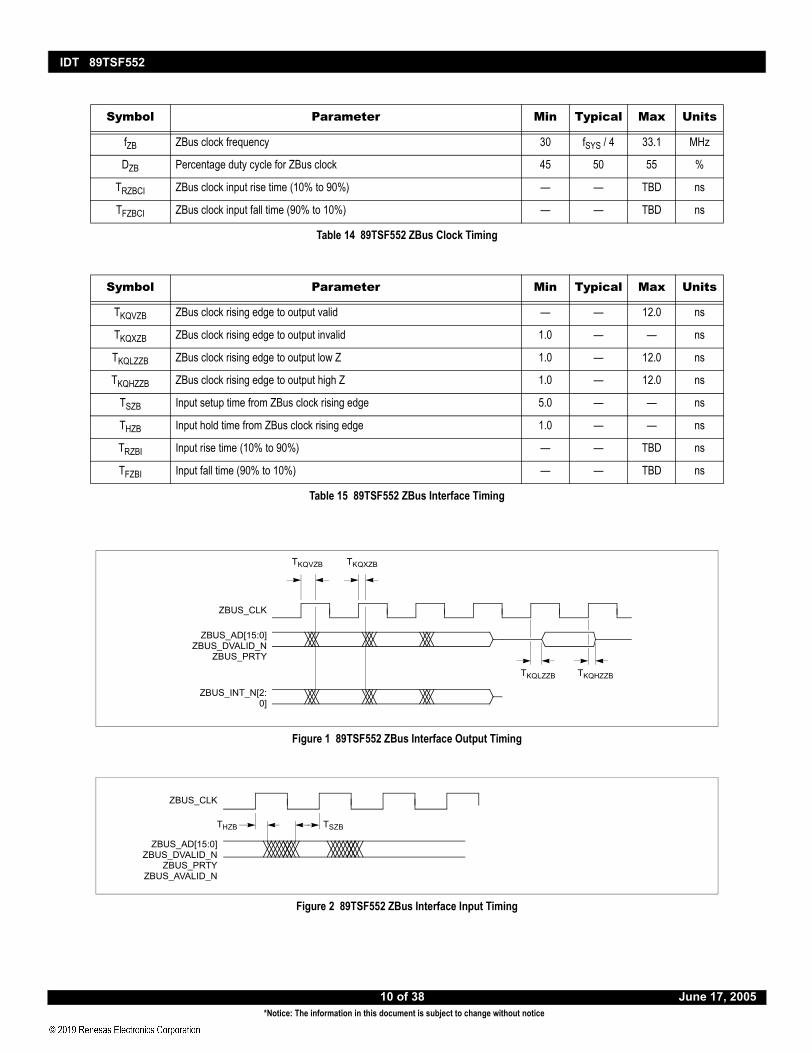
Figure 1 89TSF552 ZBus Interface Output Timing
Figure 2 89TSF552 ZBus Interface Input Timing
Symbol Parameter Min Typical Max Units
fZB ZBus clock frequency 30 fSYS / 4 33.1 MHz
DZB Percentage duty cycle for ZBus clock 45 50 55 %
TRZBCI ZBus clock input rise time (10% to 90%) — — TBD ns
TFZBCI ZBus clock input fall time (90% to 10%) — — TBD ns
Table 14 89TSF552 ZBus Clock Timing
Symbol Parameter Min Typical Max Units
TKQVZB ZBus clock rising edge to output valid — — 12.0 ns
TKQXZB ZBus clock rising edge to output invalid 1.0 — — ns
TKQLZZB ZBus clock rising edge to output low Z 1.0 — 12.0 ns
TKQHZZB ZBus clock rising edge to output high Z 1.0 — 12.0 ns
TSZB Input setup time from ZBus clock rising edge 5.0 — — ns
THZB Input hold time from ZBus clock rising edge 1.0 — — ns
TRZBI Input rise time (10% to 90%) — — TBD ns
TFZBI Input fall time (90% to 10%) — — TBD ns
Table 15 89TSF552 ZBus Interface Timing
ZBUS_CLK
TKQVZB TKQXZB
ZBUS_AD[15:0]ZBUS_DVALID_N
ZBUS_PRTY
TKQLZZB TKQHZZB
ZBUS_INT_N[2:0]
ZBUS_CLK
THZB TSZB
ZBUS_AD[15:0]ZBUS_DVALID_N
ZBUS_PRTYZBUS_AVALID_N
10 of 38 June 17, 2005*Notice: The information in this document is subject to change without notice
IDT 89TSF552
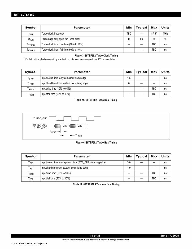
Figure 4 89TSF552 Turbo Bus Timing
Symbol Parameter Min Typical Max Units
fTUR Turbo clock frequency TBD — 87.51
1. For help with applications requiring a faster turbo interface, please contact your IDT representative.
MHz
DTUR Percentage duty cycle for Turbo clock 45 50 55 %
TRTURCI Turbo clock input rise time (10% to 90%) — — TBD ns
TFTURCI Turbo clock input fall time (90% to 10%) — — TBD ns
Figure 3 89TSF552 Turbo Clock Timing
Symbol Parameter Min Typical Max Units
TSTUR Input setup time to system clock rising edge 1.5 — — ns
THTUR Input hold time from system clock rising edge 0 — — ns
TRTURI Input rise time (10% to 90%) — — TBD ns
TFTURI Input fall time (90% to 10%) — — TBD ns
Table 16 89TSF552 Turbo Bus Timing
Symbol Parameter Min Typical Max Units
TSZT Input setup time from system clock (SYS_CLK pin) rising edge 3.0 — — ns
THZT Input hold time from system clock rising edge 1.0 — — ns
TRZTI Input rise time (10% to 90%) — — TBD ns
TFZTI Input fall time (90% to 10%) — — TBD ns
Table 17 89TSF552 ZTick Interface Timing
TURBO_CLK
TSTUR
THTUR
validvalidTURBO_SOF,TURBO_DAT
11 of 38 June 17, 2005*Notice: The information in this document is subject to change without notice
IDT 89TSF552
Symbol Parameter Min Typical Max Units Conditions
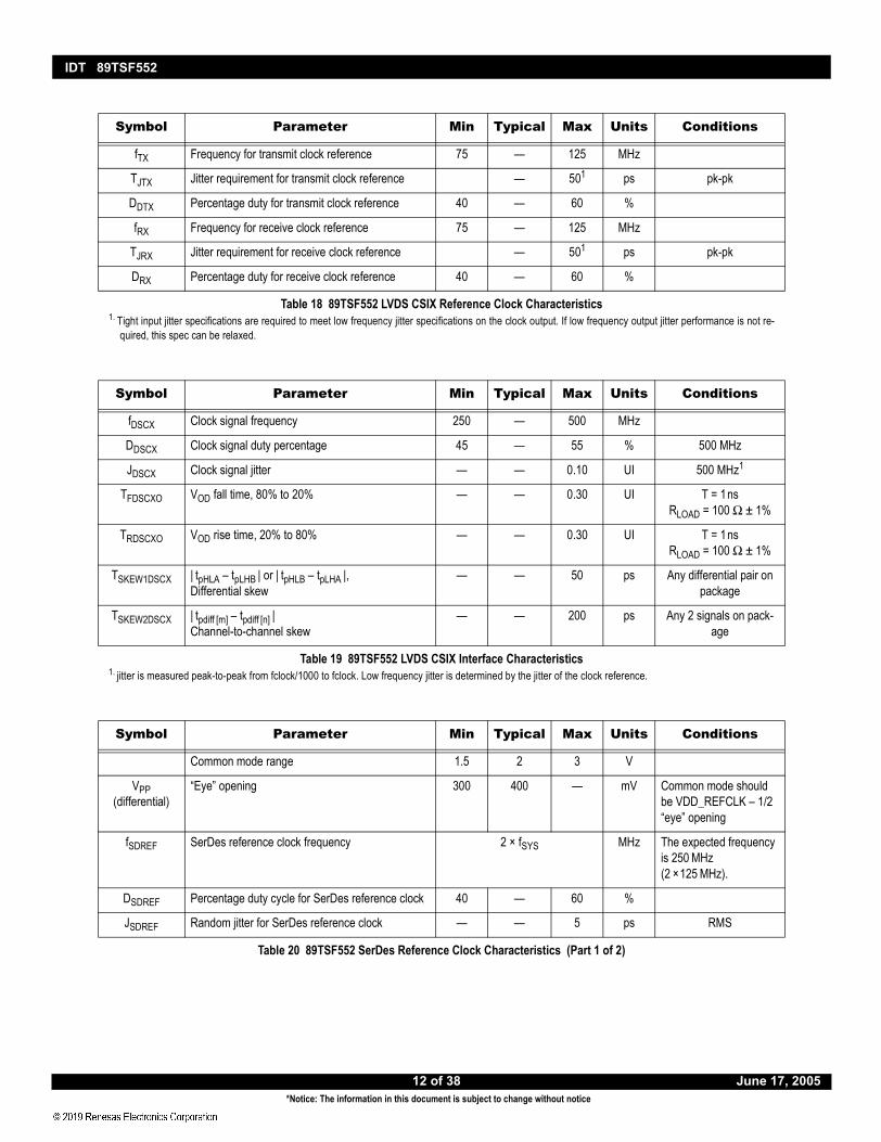
fTX Frequency for transmit clock reference 75 — 125 MHz
TJTX Jitter requirement for transmit clock reference — 501
1. Tight input jitter specifications are required to meet low frequency jitter specifications on the clock output. If low frequency output jitter performance is not re-quired, this spec can be relaxed.
ps pk-pk
DDTX Percentage duty for transmit clock reference 40 — 60 %
fRX Frequency for receive clock reference 75 — 125 MHz
TJRX Jitter requirement for receive clock reference — 501 ps pk-pk
DRX Percentage duty for receive clock reference 40 — 60 %
Table 18 89TSF552 LVDS CSIX Reference Clock Characteristics
Symbol Parameter Min Typical Max Units Conditions
fDSCX Clock signal frequency 250 — 500 MHz
DDSCX Clock signal duty percentage 45 — 55 % 500 MHz
JDSCX Clock signal jitter — — 0.10 UI 500 MHz1
1. jitter is measured peak-to-peak from fclock/1000 to fclock. Low frequency jitter is determined by the jitter of the clock reference.
TFDSCXO VOD fall time, 80% to 20% — — 0.30 UI T = 1nsRLOAD = 100 Ω ± 1%
TRDSCXO VOD rise time, 20% to 80% — — 0.30 UI T = 1nsRLOAD = 100 Ω ± 1%
TSKEW1DSCX | tpHLA – tpLHB | or | tpHLB – tpLHA |,Differential skew
— — 50 ps Any differential pair on package
TSKEW2DSCX | tpdiff [m] – tpdiff [n] |Channel-to-channel skew
— — 200 ps Any 2 signals on pack-age
Table 19 89TSF552 LVDS CSIX Interface Characteristics
Symbol Parameter Min Typical Max Units Conditions
Common mode range 1.5 2 3 V
VPP (differential)
“Eye” opening 300 400 — mV Common mode should be VDD_REFCLK – 1/2 “eye” opening
fSDREF SerDes reference clock frequency 2 × fSYS MHz The expected frequency is 250 MHz (2 ×125 MHz).
DSDREF Percentage duty cycle for SerDes reference clock 40 — 60 %
JSDREF Random jitter for SerDes reference clock — — 5 ps RMS
Table 20 89TSF552 SerDes Reference Clock Characteristics (Part 1 of 2)
12 of 38 June 17, 2005*Notice: The information in this document is subject to change without notice

IDT 89TSF552
foSDREF Frequency offset between source and target SerDes reference clocks
–100 — +100 ppm
TRSDREFCI SerDes reference clock input rise time (10% to 90%)
— — TBD ns TRZBCI
TFSDREFCI SerDes reference clock input fall time (90% to 10%)
— — TBD ns TFZBCI
Symbol Parameter Min Typical Max Units Notes
JDR Deterministic jitter at receiver — — 0.37 UI
JTR Total jitter at receiver — — 0.52 UI at 10–12 BER
ZRTERM Single-ended termination of differential inputs 45 — 55 Ω
LDR Rx return loss TBD — — dB 100 MHz to 1.875 GHz
— Rx common mode return loss TBD — — dB 100 MHz to 1.875 GHz
VRSense Input sensitivity 200 — — mV Differential peak-peak
VMAX Maximum input voltage — — 2000 mV Differential peak-peak
Treye “Eye” opening 190 — — ps
Iroff Off current –50 — 50 mA Maximum current into a pin with power off
Table 21 89TSF552 SerDes Interface Receiver Characteristics
Symbol Parameter Min Typical1
1. The typical amplitude values are obtained when VDD_TX=2.5V, and VDD_SD=1.8V
Max Units Notes
VDIFF1 Differential output (without pre-emphasis)(amplitude setting 1)
430 680 — mV Refer to Table 23.
VDIFF2 Differential output (without pre-emphasis)(amplitude setting 2)
660 1100 — mV Refer to Table 24.
VDIFF3 Differential output (without pre-emphasis)(amplitude setting 3)
700 1200 — mV Refer to Table 25.
tdrf Driver rise/fall time
Amplitude Setting 1 — — 240 ps Measured at 20–80%
Amplitude Setting 3 — — 270 ps Measured at 20–80%
ZD Differential output impedance — 100 — Ω 100 MHz to 1.875 GHz
ZSE Single-ended output impedance — 50 — Ω 100 MHz to 1.875 GHz
ZMSE Single-ended output impedance matching 3 — 8 % 100 MHz to 1.875 GHz
JD Deterministic jitter — — 0.14 UI Without pre-emphasis
JT Total jitter — — 0.38 UI At ±7 sigma
Table 22 89TSF552 SerDes Interface Transmitter Characteristics
Symbol Parameter Min Typical Max Units Conditions
Table 20 89TSF552 SerDes Reference Clock Characteristics (Part 2 of 2)
13 of 38 June 17, 2005*Notice: The information in this document is subject to change without notice

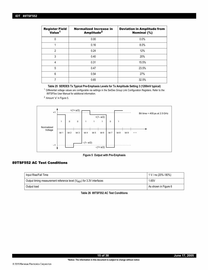
IDT 89TSF552
Register Field Value1
1. Differential voltage values are configurable via settings in the SerDes Group Link Configuration Registers. Refer to the89TSF5xx User Manual for additional information.
Normalized Increase in Amplitude2
2. Amount “a” in Figure 5.
Deviation in Amplitude from Nominal (%)
0 0.00 0.0%
1 0.31 15.5%
2 0.46 23%
3 0.77 38.5%
4 0.61 30.5%
5 0.91 45.5%
6 1.05 52.5%
7 1.29 64.5%
Table 23 SERDES Tx Typical Pre-Emphasis Levels for Tx Amplitude Setting 1 (625mV typical)
Register Field Value1
1. Differential voltage values are configurable via settings in the SerDes Group Link Configuration Registers. Refer to the89TSF5xx User Manual for additional information.
Normalized Increase in Amplitude2
2. Amount “a” in Figure 5.
Deviation in Amplitude from Nominal (%)
0 0.00 0.0%
1 0.17 8.5%
2 0.26 13%
3 0.44 22%
4 0.35 17.5%
5 0.52 26%
6 0.60 30%
7 0.73 36.5%
Table 24 SERDES Tx Typical Pre-Emphasis Levels for Tx Amplitude Setting 2 (1100mV typical)
14 of 38 June 17, 2005*Notice: The information in this document is subject to change without notice
IDT 89TSF552
Figure 5 Output with Pre-Emphasis
89TSF552 AC Test Conditions
Register Field Value1
1. Differential voltage values are configurable via settings in the SerDes Group Link Configuration Registers. Refer to the89TSF5xx User Manual for additional information.
Normalized Increase in Amplitude2
2. Amount “a” in Figure 5.
Deviation in Amplitude from Nominal (%)
0 0.00 0.0%
1 0.16 8.0%
2 0.24 12%
3 0.40 20%
4 0.31 15.5%
5 0.47 23.5%
6 0.54 27%
7 0.65 32.5%
Table 25 SERDES Tx Typical Pre-Emphasis Levels for Tx Amplitude Setting 3 (1200mV typical)
Input Rise/Fall Time 1 V / ns (20% / 80%)
Output timing measurement reference level (VREF) for 3.3V interfaces 1.65V
Output load As shown in Figure 6
Table 26 89TSF552 AC Test Conditions
bit 1 bit 2 bit 3 bit 4 bit 5 bit 6 bit 7 bit 8 bit 9 • • •
+(1+ a/2)
+(1– a/2)
–(1+ a/2)
–(1– a/2)
+1
–1
NormalizedVoltage
Bit time = 400 ps at 2.5 GHz
1 0 0 1 1 1 0 1
15 of 38 June 17, 2005*Notice: The information in this document is subject to change without notice

IDT 89TSF552
Figure 6 89TSF552 AC Test Load
89TSF552 Thermal ConsiderationsThis section describes the temperature and heat sink calculations for flip-chip BGA devices.
The thermal circuit is shown below.
Figure 7 89TSF552 Thermal Circuit
For flip-chip BGA devices, there are two paths for heat dissipation: one through the package balls to the board and other through the package caseto air. The device specifications provide ØJB and ØJC numbers. The ØCA number comes from the heat sink manufacturer and depends on type of heatsink (area, height, fin type, etc.) and the airflow across the heat sink. The device specifications also provide the maximum operating junction tempera-ture (TJ) that will not degrade the device reliability. The system designer should ensure that the device maximum junction temperature is not exceededunder any operating condition. One method of accomplishing this is to calculate the maximum ambient temperature (TA) that can be tolerated basedon the above device parameters. The formula is shown below.
ØJB x (ØJC + ØCA) TA = TJ - W x --------------------------- ØJB + ØJC + ØCA
Symbol Parameter Value Units Conditions
ØJA Thermal resistance, junction to ambient (no heat sink) 9.0 °C / W Still air
5.5 °C / W 200 FPM
4.5 °C / W 500 FPM
ØJB Estimated thermal resistance, junction to board 2.2 °C / W
ØJC Thermal resistance, junction to case 0.19 °C / W
Table 27 89TSF552 Thermal Characteristics
Z0 = 50Ω
50Ω
5 pFVREF100Ω
100Ω
VDD
20 pF
For enable/disable spec
For output timing
ØJB TA W2 (dissipated through board) TJ Total Power = W TA W1 ØJC ØCA
Device
16 of 38 June 17, 2005*Notice: The information in this document is subject to change without notice

IDT 89TSF552
The following graph depicts the ambient temperature (TA) versus ØCA.
Figure 8 89TSF552 Ambient Temperature Curve
For system designers, specification of the maximum device junction temperature (operating) is critical, since it allows them to select a heat sinkthat meets the maximum ambient temperature requirements of their system.
The other parameter that is device package-specific is ØJA, without a heat sink, and is specified for various air-flow conditions. This is the intrinsicthermal resistance of the package (junction to case + case to ambient) and is mainly specified as a reference parameter. (This is when a heat sink isnot present and the top surface of the package is essentially acting as the heat sink). However, in devices that have high power dissipation, heat sinkusage is highly desirable. Consequently, system designers may have limited use for this parameter.
89TSF552 Power, Reset, and Initialization Sequencing Requirements
Power Supply Power-Up SequenceThere is a power supply power-up sequence requirement that addresses potential latchup issues with some I/O buffers. All 3.3V I/O power must
ramp up before all other power supply pins:– 3.3V I/O (VDD_IO, VDDP33, VDD_REFCLKn)– all other power supply pins
Further, IDT recommends that the designer use current limiting resistors on the bidirectional ZBus pins to limit potential high transient current fromshort-circuit current or bus contention during the power-up period. Such events can occur because of an unknown state of output enable of the bidirec-tional buffers. After core power ramps up (with RESET_N asserted), the bidirectional I/O lines enter normal operating mode.
Power Supply Power-Down Sequence Because the power supply power-off state clears any latchup condition, the power-down sequence is not dictated by latchup.However, potential high transient current from short-circuit current or bus contention can also occur during the power-down period. We recommend
appropriate sequencing. All 3.3V I/O power should ramp down before the 1.8V core (VDD) power:– 3.3V I/O (VDD_IO)– 1.8V core (VDD)
Ambient Temp. vs ØCA
70.8
64.861.0
58.556.6 55.1 54.0 53.1
30.0
40.0
50.0
60.0
70.0
80.0
1.0 2.0 3.0 4.0 5.0 6.0 7.0 8.0
ØCA oC/W
T A
o C
17 of 38 June 17, 2005*Notice: The information in this document is subject to change without notice

IDT 89TSF552
However, if appropriate current limiting techniques (e.g., series resistors) are employed and the 2.5V and 1.5V power supplies ramp down soonafter the 1.8V core power supply (within about 50 ms), the system designer can safely ignore this recommendation.
PLL Power-Up Initialization PLL inputs into the 89TSF552, from an external device such as the ZBus bridge in IDT’s reference system, require a special initialization
sequence. Figure 9 shows the initialization sequence.PLL initialization is necessary only at power-up. If the PLLs fail to lock, repeatedly assert PLL_RST until they do.
Note: The 89TSF552 must be reset after PLL initialization. Hold RESET_N low for at least 16 clocks (SYS_CLK) after PLL initialization completes.
Figure 9 PLL Power-Up Initialization for the 89TSF552
Device Reset It is possible to reset the entire 89TSF552 device except for the PLL. To reset the device without being required to re-initialize the PLL, assert the
RESET_N pin (low) for at least 16 clocks (SYS_CLK) and then deassert it.
Pin List I/O DescriptionThe 89TSF552 Pin List on page 19 uses the following I/O notations:
I Input
O Output
B Bidirectional
P Power
DNC Do not connect
RPD Reserved, pulldwn. Pin must be connected to VSS through a 300 - 1K Ω resistor.
RPU Reserved, pullup. Pin is connected to VDD_IO (3.3V) through a 1K - 10K Ω resistor.
PLL_DIV_RST_N
1 µs min
TACQUIRE, 15 µs min
PLL_SYS_LCK
10 ns min
PLL_RST
Repeat if necessary until lock is achieved.
RESET_N
TRESET, 16 clocks min
Power Supplies
Clockclock present and stable
···
18 of 38 June 17, 2005*Notice: The information in this document is subject to change without notice

IDT 89TSF552
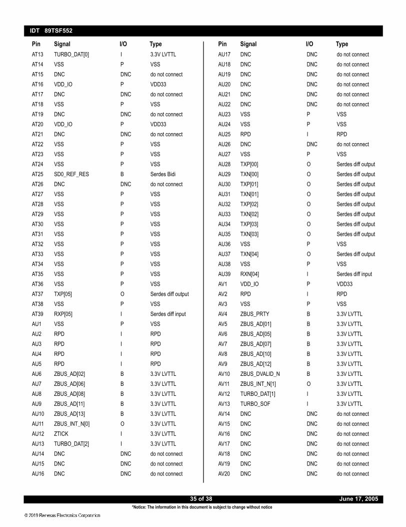
89TSF552 Pin ListPin Signal I/O TypeA2 DNC DNC do not connectA3 RPD I RPDA4 VDD_IO P VDD33A5 DNC DNC do not connectA6 VSS P VSSA7 DNC DNC do not connectA8 VDD_IO P VDD33A9 DNC DNC do not connectA10 VSS P VSSA11 DNC DNC do not connectA12 DNC DNC do not connectA13 DNC DNC do not connectA14 VSS P VSSA15 DNC DNC do not connectA16 VDD_IO P VDD33A17 DNC DNC do not connectA18 VSS P VSSA19 DNC DNC do not connectA20 VSS P VSSA21 SYS_CLK I 3.3V LVTTLA22 VSS P VSSA23 RPD I RPDA24 VSS P VSSA25 SD2_REFCLKN I Serdes diff clockA26 SD2_REFCLKP I Serdes diff clockA27 VSS P VSSA28 RXN[23] I Serdes diff inputA29 RXP[23] I Serdes diff inputA30 RXN[22] I Serdes diff inputA31 RXP[22] I Serdes diff inputA32 RXN[21] I Serdes diff inputA33 RXP[21] I Serdes diff inputA34 RXN[20] I Serdes diff inputA35 RXP[20] I Serdes diff inputA36 VSS P VSSA37 VSS P VSSA38 VSS P VSSB1 VSS P VSSB2 DNC DNC do not connectB3 DNC DNC do not connectB4 DNC DNC do not connectB5 DNC DNC do not connect
19 of *Notice: The information in this documen
Pin Signal I/O TypeB6 DNC DNC do not connectB7 DNC DNC do not connectB8 DNC DNC do not connectB9 DNC DNC do not connectB10 DNC DNC do not connectB11 DNC DNC do not connectB12 DNC DNC do not connectB13 DNC DNC do not connectB14 DNC DNC do not connectB15 DNC DNC do not connectB16 DNC DNC do not connectB17 DNC DNC do not connectB18 VDD_IO P VDD33B19 PLL_SYS_LCK O 3.3V LVTTLB20 VSS P VSSB21 VSS P VSSB22 VSS P VSSB23 RPD I RPDB24 VSS P VSSB25 VSS P VSSB26 VSS P VSSB27 VSS P VSSB28 VSS P VSSB29 VSS P VSSB30 VSS P VSSB31 VSS P VSSB32 VSS P VSSB33 VSS P VSSB34 VSS P VSSB35 VSS P VSSB36 VSS P VSSB37 VSS P VSSB38 VSS P VSSB39 VSS P VSSC1 VDD_IO P VDD33C2 DNC DNC do not connectC3 DNC DNC do not connectC4 DNC DNC do not connectC5 DNC DNC do not connectC6 DNC DNC do not connectC7 DNC DNC do not connectC8 DNC DNC do not connectC9 DNC DNC do not connect
38 June 17, 2005t is subject to change without notice

IDT 89TSF552
Pin Signal I/O TypeC10 DNC DNC do not connectC11 DNC DNC do not connectC12 DNC DNC do not connectC13 DNC DNC do not connectC14 DNC DNC do not connectC15 DNC DNC do not connectC16 DNC DNC do not connectC17 DNC DNC do not connectC18 TDO I 3.3V LVTTLC19 TRST_N I 3.3V LVTTLC20 RPU I RPUC21 DNC DNC do not connectC22 PLL_RST I 3.3V LVTTLC23 RPD I RPDC24 VSS P VSSC25 DNC DNC do not connectC26 RPD I RPDC27 VSS P VSSC28 TXN[23] O Serdes diff outputC29 TXP[23] O Serdes diff outputC30 TXN[22] O Serdes diff outputC31 TXP[22] O Serdes diff outputC32 TXN[21] O Serdes diff outputC33 TXP[21] O Serdes diff outputC34 TXN[20] O Serdes diff outputC35 TXP[20] O Serdes diff outputC36 VSS P VSSC37 TXN[19] O Serdes diff outputC38 VSS P VSSC39 RXN[19] I Serdes diff inputD1 DNC DNC do not connectD2 DNC DNC do not connectD3 DNC DNC do not connectD4 VSS P VSSD5 DNC DNC do not connectD6 VDD_IO P VDD33D7 DNC DNC do not connectD8 DNC DNC do not connectD9 VSS P VSSD10 VDD_IO P VDD33D11 DNC DNC do not connectD12 VSS P VSSD13 DNC DNC do not connect
20 of *Notice: The information in this documen
Pin Signal I/O TypeD14 DNC DNC do not connectD15 DNC DNC do not connectD16 VSS P VSSD17 DNC DNC do not connectD18 VDD_IO P VDD33D19 TMS I 3.3V LVTTLD20 VSS P VSSD21 DNC DNC do not connectD22 PLL_DIV_RST_N I 3.3V LVTTLD23 RPD I RPDD24 VSS P VSSD25 DNC DNC do not connectD26 SD2_REF_RES B Serdes BidiD27 VSS P VSSD28 VSS P VSSD29 VSS P VSSD30 VSS P VSSD31 VSS P VSSD32 VSS P VSSD33 VSS P VSSD34 VSS P VSSD35 VSS P VSSD36 VSS P VSSD37 TXP[19] O Serdes diff outputD38 VSS P VSSD39 RXP[19] I Serdes diff inputE1 VSS P VSSE2 DNC DNC do not connectE3 DNC DNC do not connectE4 VDD_IO P VDD33E5 RPD I RPDE6 RPD I RPDE7 VSS P VSSE8 VDD_IO P VDD33E9 DNC DNC do not connectE10 DNC DNC do not connectE11 DNC DNC do not connectE12 DNC DNC do not connectE13 DNC DNC do not connectE14 DNC DNC do not connectE15 DNC DNC do not connectE16 DNC DNC do not connectE17 DNC DNC do not connect
38 June 17, 2005t is subject to change without notice

IDT 89TSF552
Pin Signal I/O TypeE18 RPD I RPDE19 TCK I 3.3V LVTTLE20 RPU I RPUE21 DNC DNC do not connectE22 DNC DNC do not connectE23 DNC DNC do not connectE24 DNC DNC do not connectE25 DNC DNC do not connectE26 VSS P VSSE27 DNC DNC do not connectE28 DNC DNC do not connectE29 DNC DNC do not connectE30 DNC DNC do not connectE31 DNC DNC do not connectE32 DNC DNC do not connectE33 DNC DNC do not connectE34 DNC DNC do not connectE35 DNC DNC do not connectE36 VSS P VSSE37 TXN[18] O Serdes diff outputE38 VSS P VSSE39 RXN[18] I Serdes diff inputF1 CTX_REFCLK I 3.3V LVTTLF2 VSS P VSSF3 DNC DNC do not connectF4 DNC DNC do not connectF5 RPD I RPDF6 RPD I RPDF7 RPD I RPDF8 DNC DNC do not connectF9 DNC DNC do not connectF10 DNC DNC do not connectF11 DNC DNC do not connectF12 DNC DNC do not connectF13 DNC DNC do not connectF14 DNC DNC do not connectF15 DNC DNC do not connectF16 DNC DNC do not connectF17 DNC DNC do not connectF18 DNC DNC do not connectF19 TDI I 3.3V LVTTLF20 DNC DNC do not connectF21 DNC DNC do not connect
21 of *Notice: The information in this documen
Pin Signal I/O TypeF22 DNC DNC do not connectF23 DNC DNC do not connectF24 DNC DNC do not connectF25 DNC DNC do not connectF26 DNC DNC do not connectF27 DNC DNC do not connectF28 DNC DNC do not connectF29 DNC DNC do not connectF30 DNC DNC do not connectF31 DNC DNC do not connectF32 DNC DNC do not connectF33 DNC DNC do not connectF34 DNC DNC do not connectF35 DNC DNC do not connectF36 VSS P VSSF37 TXP[18] O Serdes diff outputF38 VSS P VSSF39 RXP[18] I Serdes diff inputG1 VDD25 P VDD25G2 VSS P VSSG3 PLL_CTX_RST I 3.3V LVTTLG4 PLL_CTX_LCK O 3.3V LVTTLG5 VSS P VSSG6 RPD I RPDG7 DNC DNC do not connectG8 DNC DNC do not connectG9 DNC DNC do not connectG10 DNC DNC do not connectG11 DNC DNC do not connectG12 DNC DNC do not connectG13 DNC DNC do not connectG14 DNC DNC do not connectG15 DNC DNC do not connectG16 DNC DNC do not connectG17 DNC DNC do not connectG18 DNC DNC do not connectG19 DNC DNC do not connectG20 DNC DNC do not connectG21 DNC DNC do not connectG22 DNC DNC do not connectG23 DNC DNC do not connectG24 DNC DNC do not connectG25 DNC DNC do not connect
38 June 17, 2005t is subject to change without notice

IDT 89TSF552
Pin Signal I/O TypeG26 DNC DNC do not connectG27 DNC DNC do not connectG28 DNC DNC do not connectG29 DNC DNC do not connectG30 DNC DNC do not connectG31 DNC DNC do not connectG32 DNC DNC do not connectG33 DNC DNC do not connectG34 DNC DNC do not connectG35 DNC DNC do not connectG36 VSS P VSSG37 TXN[17] O Serdes diff outputG38 VSS P VSSG39 RXN[17] I Serdes diff inputH1 CTX_CTRL_CLKP I LVDSH2 CTX_CTRL_CLKN I LVDSH3 CTX_CTRL_DATP[2] I LVDSH4 CTX_CTRL_DATN[2] I LVDSH5 CTX_CTRL_SOFP I LVDSH6 CTX_CTRL_SOFN I LVDSH7 DNC DNC do not connectH8 DNC DNC do not connectH9 DNC DNC do not connectH10 DNC DNC do not connectH11 DNC DNC do not connectH12 DNC DNC do not connectH13 DNC DNC do not connectH14 DNC DNC do not connectH15 DNC DNC do not connectH16 DNC DNC do not connectH17 DNC DNC do not connectH18 DNC DNC do not connectH19 DNC DNC do not connectH20 DNC DNC do not connectH21 PLL_SYS_VDD P 1.8V VDDH22 DNC DNC do not connectH23 DNC DNC do not connectH24 DNC DNC do not connectH25 DNC DNC do not connectH26 DNC DNC do not connectH27 DNC DNC do not connectH28 DNC DNC do not connectH29 DNC DNC do not connect
22 of *Notice: The information in this documen
Pin Signal I/O TypeH30 DNC DNC do not connectH31 DNC DNC do not connectH32 DNC DNC do not connectH33 DNC DNC do not connectH34 DNC DNC do not connectH35 DNC DNC do not connectH36 VSS P VSSH37 TXP[17] O Serdes diff outputH38 VSS P VSSH39 RXP[17] I Serdes diff inputJ1 VSS P VSSJ2 CTX_CTRL_DATP[0] I LVDSJ3 CTX_CTRL_DATN[0] I LVDSJ4 VDD25 P VDD25J5 CTX_CTRL_DATP[3] I LVDSJ6 CTX_CTRL_DATN[3] I LVDSJ7 VDD25 P VDD25J8 DNC DNC do not connectJ9 DNC DNC do not connectJ10 DNC DNC do not connectJ11 DNC DNC do not connectJ12 DNC DNC do not connectJ13 DNC DNC do not connectJ14 DNC DNC do not connectJ15 DNC DNC do not connectJ16 DNC DNC do not connectJ17 DNC DNC do not connectJ18 DNC DNC do not connectJ19 DNC DNC do not connectJ20 PLL_SYS_VSSA P AVSSJ21 PLL_SYS_VSS P VSSJ22 DNC DNC do not connectJ23 VDD_SD2_PLL P VAA18J24 VDD_REFCLK2 P VAA33J25 DNC DNC do not connectJ26 DNC DNC do not connectJ27 VSS P VSSJ28 DNC DNC do not connectJ29 DNC DNC do not connectJ30 DNC DNC do not connectJ31 DNC DNC do not connectJ32 DNC DNC do not connectJ33 DNC DNC do not connect
38 June 17, 2005t is subject to change without notice

IDT 89TSF552
Pin Signal I/O TypeJ34 DNC DNC do not connectJ35 DNC DNC do not connectJ36 VSS P VSSJ37 TXN[16] O Serdes diff outputJ38 VSS P VSSJ39 RXN[16] I Serdes diff inputK1 CTX_DATP[15] O LVDSK2 CTX_DATN[15] O LVDSK3 CTX_SOFP O LVDSK4 CTX_SOFN O LVDSK5 CTX_CTRL_DATP[1] I LVDSK6 CTX_CTRL_DATN[1] I LVDSK7 VDD25 P VDD25K8 DNC DNC do not connectK9 DNC DNC do not connectK10 DNC DNC do not connectK11 DNC DNC do not connectK12 DNC DNC do not connectK13 DNC DNC do not connectK14 DNC DNC do not connectK15 DNC DNC do not connectK16 DNC DNC do not connectK17 DNC DNC do not connectK18 DNC DNC do not connectK19 DNC DNC do not connectK20 PLL_SYS_VDDA P 3.3V AVDDK21 DNC DNC do not connectK22 VSS_SD2_PLL P VSSK23 VSS P VSSK24 VSS P VSSK25 VSS P VSSK26 VSS P VSSK27 VSS P VSSK28 VSS P VSSK29 VSS P VSSK30 VSS P VSSK31 DNC DNC do not connectK32 DNC DNC do not connectK33 DNC DNC do not connectK34 DNC DNC do not connectK35 DNC DNC do not connectK36 VSS P VSSK37 TXP[16] O Serdes diff output
23 of *Notice: The information in this documen
Pin Signal I/O TypeK38 VSS P VSSK39 RXP[16] I Serdes diff inputL1 VDD25 P VDD25L2 CTX_DATP[13] O LVDSL3 CTX_DATN[13] O LVDSL4 VSS P VSSL5 CTX_CTRL_PRTYP I LVDSL6 CTX_CTRL_PRTYN I LVDSL7 VSS P VSSL8 DNC DNC do not connectL9 DNC DNC do not connectL10 DNC DNC do not connectL11 VSS P VSSL12 VSS P VSSL13 VSS P VSSL14 VSS P VSSL15 VSS P VSSL16 VSS P VSSL17 VSS P VSSL18 VSS P VSSL19 VSS P VSSL20 VSS P VSSL21 VSS P VSSL22 DNC DNC do not connectL23 VSS P VSSL24 VSS P VSSL25 VSS P VSSL26 VSS P VSSL27 VSS P VSSL28 VSS P VSSL29 VSS P VSSL30 VSS P VSSL31 DNC DNC do not connectL32 DNC DNC do not connectL33 DNC DNC do not connectL34 DNC DNC do not connectL35 DNC DNC do not connectL36 VSS P VSSL37 TXN[15] O Serdes diff outputL38 VSS P VSSL39 RXN[15] I Serdes diff inputM1 CTX_DATP[10] O LVDSM2 CTX_DATN[10] O LVDS
38 June 17, 2005t is subject to change without notice

IDT 89TSF552
Pin Signal I/O TypeM3 CTX_DATP[12] O LVDSM4 CTX_DATN[12] O LVDSM5 CTX_DATP[14] O LVDSM6 CTX_DATN[14] O LVDSM7 VSS P VSSM8 DNC DNC do not connectM9 DNC DNC do not connectM10 DNC DNC do not connectM11 VSS P VSSM12 VSS P VSSM13 VSS P VSSM14 VSS P VSSM15 VSS P VSSM16 VSS P VSSM17 VSS P VSSM18 VSS P VSSM19 VSS P VSSM20 VSS P VSSM21 VSS P VSSM22 DNC DNC do not connectM23 VDD_TX P VAA25M24 VDD_TX P VAA25M25 VDD_TX P VAA25M26 VDD_TX P VAA25M27 VDD_TX P VAA25M28 VDD_TX P VAA25M29 VSS P VSSM30 VSS P VSSM31 DNC DNC do not connectM32 DNC DNC do not connectM33 DNC DNC do not connectM34 DNC DNC do not connectM35 DNC DNC do not connectM36 VSS P VSSM37 TXP[15] O Serdes diff outputM38 VSS P VSSM39 RXP[15] I Serdes diff inputN1 VSS P VSSN2 CTX_DATP[8] O LVDSN3 CTX_DATN[8] O LVDSN4 VDD25 P VDD25N5 CTX_DATP[11] O LVDSN6 CTX_DATN[11] O LVDS
24 of *Notice: The information in this documen
Pin Signal I/O TypeN7 VDD25 P VDD25N8 DNC DNC do not connectN9 DNC DNC do not connectN10 DNC DNC do not connectN11 VSS P VSSN12 VSS P VSSN13 VDD_IO P VDD33N14 VDD_IO P VDD33N15 VDD_IO P VDD33N16 VDD_IO P VDD33N17 VDD_IO P VDD33N18 VDD_IO P VDD33N19 VDD_IO P VDD33N20 VDD_IO P VDD33N21 VDD_IO P VDD33N22 DNC DNC do not connectN23 VDD_SD P VAA18N24 VDD_SD P VAA18N25 VDD_SD P VAA18N26 VDD_SD P VAA18N27 VDD_SD P VAA18N28 VDD_TX P VAA25N29 VSS P VSSN30 VSS P VSSN31 DNC DNC do not connectN32 DNC DNC do not connectN33 DNC DNC do not connectN34 DNC DNC do not connectN35 DNC DNC do not connectN36 VSS P VSSN37 TXN[14] O Serdes diff outputN38 VSS P VSSN39 RXN[14] I Serdes diff inputP1 CTX_CLKP O LVDSP2 CTX_CLKN O LVDSP3 CTX_DATP[7] O LVDSP4 CTX_DATN[7] O LVDSP5 CTX_DATP[9] O LVDSP6 CTX_DATN[9] O LVDSP7 VDD25 P VDD25P8 DNC DNC do not connectP9 DNC DNC do not connectP10 DNC DNC do not connect
38 June 17, 2005t is subject to change without notice

IDT 89TSF552
Pin Signal I/O TypeP11 VSS P VSSP12 VSS P VSSP13 VDD_IO P VDD33P14 VSS P VSSP15 VDD P VDD18P16 VDD P VDD18P17 VSS P VSSP18 VSS P VSSP19 VDD P VDD18P20 VDD P VDD18P21 VSS P VSSP22 VSS P VSSP23 VSS P VSSP24 VSS P VSSP25 VSS P VSSP26 VSS P VSSP27 VDD_SD P VAA18P28 VDD_TX P VAA25P29 VSS P VSSP30 VSS P VSSP31 DNC DNC do not connectP32 DNC DNC do not connectP33 DNC DNC do not connectP34 DNC DNC do not connectP35 DNC DNC do not connectP36 VSS P VSSP37 TXP[14] O Serdes diff outputP38 VSS P VSSP39 RXP[14] I Serdes diff inputR1 VDD25 P VDD25R2 CTX_DATP[6] O LVDSR3 CTX_DATN[6] O LVDSR4 VSS P VSSR5 CTX_DATP[4] O LVDSR6 CTX_DATN[4] O LVDSR7 VSS P VSSR8 DNC DNC do not connectR9 DNC DNC do not connectR10 DNC DNC do not connectR11 VSS P VSSR12 VSS P VSSR13 VDDP33 P VDDP33R14 VSS P VSS
25 of *Notice: The information in this documen
Pin Signal I/O TypeR15 VDD P VDD18R16 VDD P VDD18R17 VSS P VSSR18 VSS P VSSR19 VDD P VDD18R20 VDD P VDD18R21 VSS P VSSR22 VSS P VSSR23 VSS P VSSR24 VSS P VSSR25 VSS P VSSR26 VSS P VSSR27 VDD_SD P VAA18R28 VDD_TX P VAA25R29 VSS P VSSR30 VSS P VSSR31 DNC DNC do not connectR32 DNC DNC do not connectR33 DNC DNC do not connectR34 DNC DNC do not connectR35 DNC DNC do not connectR36 VSS P VSSR37 TXN[13] O Serdes diff outputR38 VSS P VSSR39 RXN[13] I Serdes diff inputT1 CTX_DATP[2] O LVDST2 CTX_DATN[2] O LVDST3 CTX_DATP[3] O LVDST4 CTX_DATN[3] O LVDST5 CTX_DATP[5] O LVDST6 CTX_DATN[5] O LVDST7 VSS P VSST8 DNC DNC do not connectT9 PLL_CTX_VDDA P 3.3V AVDDT10 PLL_CTX_VSSA P AVSST11 VSS P VSST12 VSS P VSST13 VDDP33 P VDDP33T14 VSS P VSST15 VDD P VDD18T16 VDD P VDD18T17 VSS P VSST18 VSS P VSS
38 June 17, 2005t is subject to change without notice

IDT 89TSF552
Pin Signal I/O TypeT19 VDD P VDD18T20 VDD P VDD18T21 VSS P VSST22 VSS P VSST23 VDD P VDD18T24 VDD P VDD18T25 VSS P VSST26 VSS P VSST27 VDD_SD P VAA18T28 VDD_TX P VAA25T29 VSS P VSST30 VSS P VSST31 DNC DNC do not connectT32 DNC DNC do not connectT33 DNC DNC do not connectT34 DNC DNC do not connectT35 DNC DNC do not connectT36 VSS P VSST37 TXP[13] O Serdes diff outputT38 VSS P VSST39 RXP[13] I Serdes diff inputU1 VSS P VSSU2 CTX_DATP[0] O LVDSU3 CTX_DATN[0] O LVDSU4 VDD25 P VDD25U5 CTX_DATP[1] O LVDSU6 CTX_DATN[1] O LVDSU7 VDD25 P VDD25U8 DNC DNC do not connectU9 PLL_CTX_VDD P 1.8V AVDDU10 PLL_CTX_VSS P VSSU11 VSS P VSSU12 VSS P VSSU13 VDD25 P VDD25U14 VSS P VSSU15 VDD P VDD18U16 VDD P VDD18U17 VSS P VSSU18 VSS P VSSU19 VDD P VDD18U20 VDD P VDD18U21 VSS P VSSU22 VSS P VSS
26 of *Notice: The information in this documen
Pin Signal I/O TypeU23 VDD P VDD18U24 VDD P VDD18U25 VSS P VSSU26 VSS P VSSU27 VDD_SD P VAA18U28 VDD_TX P VAA25U29 VSS P VSSU30 VSS P VSSU31 DNC DNC do not connectU32 DNC DNC do not connectU33 DNC DNC do not connectU34 DNC DNC do not connectU35 DNC DNC do not connectU36 VSS P VSSU37 TXN[12] O Serdes diff outputU38 VSS P VSSU39 RXN[12] I Serdes diff inputV1 CRX_DATN[0] I LVDSV2 CRX_DATP[0] I LVDSV3 CRX_PRTYN I LVDSV4 CRX_PRTYP I LVDSV5 CTX_PRTYP O LVDSV6 CTX_PRTYN O LVDSV7 VDD25 P VDD25V8 DNC DNC do not connectV9 DNC DNC do not connectV10 DNC DNC do not connectV11 VSS P VSSV12 VSS P VSSV13 VDD25 P VDD25V14 VSS P VSSV15 VDD P VDD18V16 VDD P VDD18V17 VSS P VSSV18 VSS P VSSV19 VDD P VDD18V20 VDD P VDD18V21 VSS P VSSV22 VSS P VSSV23 VDD P VDD18V24 VDD P VDD18V25 VSS P VSSV26 VSS P VSS
38 June 17, 2005t is subject to change without notice
IDT 89TSF552
Pin Signal I/O TypeV27 VDD_SD P VAA18V28 VDD_TX P VAA25V29 VSS P VSSV30 VSS P VSSV31 DNC DNC do not connectV32 DNC DNC do not connectV33 DNC DNC do not connectV34 DNC DNC do not connectV35 DNC DNC do not connectV36 VSS P VSSV37 TXP[12] O Serdes diff outputV38 VSS P VSSV39 RXP[12] I Serdes diff inputW1 VDD25 P VDD25W2 CRX_DATN[2] I LVDSW3 CRX_DATP[2] I LVDSW4 VSS P VSSW5 CRX_DATN[1] I LVDSW6 CRX_DATP[1] I LVDSW7 VSS P VSSW8 DNC DNC do not connectW9 DNC DNC do not connectW10 VDD12 P VDD12W11 VSS P VSSW12 VSS P VSSW13 VDD25 P VDD25W14 VSS P VSSW15 VDD P VDD18W16 VDD P VDD18W17 VSS P VSSW18 VSS P VSSW19 VDD P VDD18W20 VDD P VDD18W21 VSS P VSSW22 VSS P VSSW23 VDD P VDD18W24 VDD P VDD18W25 VSS P VSSW26 VSS P VSSW27 VDD_SD P VAA18W28 VDD_TX P VAA25W29 VSS P VSSW30 VSS P VSS
27 of *Notice: The information in this documen
Pin Signal I/O TypeW31 VSS_SD1_PLL P VSSW32 DNC DNC do not connectW33 DNC DNC do not connectW34 DNC DNC do not connectW35 DNC DNC do not connectW36 VSS P VSSW37 VSS P VSSW38 VSS P VSSW39 VSS P VSSY1 CRX_DATN[5] I LVDSY2 CRX_DATP[5] I LVDSY3 CRX_DATN[4] I LVDSY4 CRX_DATP[4] I LVDSY5 CRX_DATN[3] I LVDSY6 CRX_DATP[3] I LVDSY7 VSS P VSSY8 DNC DNC do not connectY9 DNC DNC do not connectY10 DNC DNC do not connectY11 VSS P VSSY12 VSS P VSSY13 VDDP33 P VDDP33Y14 VSS P VSSY15 VDD P VDD18Y16 VDD P VDD18Y17 VSS P VSSY18 VSS P VSSY19 VDD P VDD18Y20 VDD P VDD18Y21 VSS P VSSY22 VSS P VSSY23 VDD P VDD18Y24 VDD P VDD18Y25 VSS P VSSY26 VSS P VSSY27 VDD_SD P VAA18Y28 VDD_TX P VAA25Y29 VSS P VSSY30 VSS P VSSY31 VDD_SD1_PLL P VAA18Y32 DNC DNC do not connectY33 DNC DNC do not connectY34 DNC DNC do not connect
38 June 17, 2005t is subject to change without notice
IDT 89TSF552
Pin Signal I/O TypeY35 DNC DNC do not connectY36 DNC DNC do not connectY37 DNC DNC do not connectY38 VSS P VSSY39 SD1_REFCLKN I Serdes diff clockAA1 VSS P VSSAA2 CRX_DATN[7] I LVDSAA3 CRX_DATP[7] I LVDSAA4 VDD25 P VDD25AA5 CRX_DATN[6] I LVDSAA6 CRX_DATP[6] I LVDSAA7 VDD25 P VDD25AA8 DNC DNC do not connectAA9 DNC DNC do not connectAA10 VDD12 P VDD12AA11 VSS P VSSAA12 VSS P VSSAA13 VDDP33 P VDDP33AA14 VSS P VSSAA15 VDD P VDD18AA16 VDD P VDD18AA17 VSS P VSSAA18 VSS P VSSAA19 VDD P VDD18AA20 VDD P VDD18AA21 VSS P VSSAA22 VSS P VSSAA23 VDD P VDD18AA24 VDD P VDD18AA25 VSS P VSSAA26 VSS P VSSAA27 VDD_SD P VAA18AA28 VDD_TX P VAA25AA29 VSS P VSSAA30 VSS P VSSAA31 VDD_REFCLK1 P VAA33AA32 DNC DNC do not connectAA33 DNC DNC do not connectAA34 VSS P VSSAA35 VSS P VSSAA36 SD1_REF_RES B Serdes BidiAA37 RPD I RPDAA38 VSS P VSS
28 of *Notice: The information in this documen
Pin Signal I/O TypeAA39 SD1_REFCLKP I Serdes diff clockAB1 CRX_CLKN I LVDSAB2 CRX_CLKP I LVDSAB3 CRX_DATN[8] I LVDSAB4 CRX_DATP[8] I LVDSAB5 CRX_DATN[9] I LVDSAB6 CRX_DATP[9] I LVDSAB7 VDD25 P VDD25AB8 DNC DNC do not connectAB9 DNC DNC do not connectAB10 DNC DNC do not connectAB11 VSS P VSSAB12 VSS P VSSAB13 VDDP33 P VDDP33AB14 VSS P VSSAB15 VDD P VDD18AB16 VDD P VDD18AB17 VSS P VSSAB18 VSS P VSSAB19 VDD P VDD18AB20 VDD P VDD18AB21 VSS P VSSAB22 VSS P VSSAB23 VDD P VDD18AB24 VDD P VDD18AB25 VSS P VSSAB26 VSS P VSSAB27 VDD_SD P VAA18AB28 VDD_TX P VAA25AB29 VSS P VSSAB30 VSS P VSSAB31 DNC DNC do not connectAB32 DNC DNC do not connectAB33 DNC DNC do not connectAB34 DNC DNC do not connectAB35 DNC DNC do not connectAB36 VSS P VSSAB37 VSS P VSSAB38 VSS P VSSAB39 VSS P VSSAC1 VDD25 P VDD25AC2 CRX_DATN[10] I LVDSAC3 CRX_DATP[10] I LVDS
38 June 17, 2005t is subject to change without notice
IDT 89TSF552
Pin Signal I/O TypeAC4 VSS P VSSAC5 CRX_DATN[11] I LVDSAC6 CRX_DATP[11] I LVDSAC7 VSS P VSSAC8 DNC DNC do not connectAC9 PLL_CRX_VDDA P 3.3V AVDDAC10 PLL_CRX_VSSA P AVSSAC11 VSS P VSSAC12 VSS P VSSAC13 VDD25 P VDD25AC14 VSS P VSSAC15 VDD P VDD18AC16 VDD P VDD18AC17 VSS P VSSAC18 VSS P VSSAC19 VDD P VDD18AC20 VDD P VDD18AC21 VSS P VSSAC22 VSS P VSSAC23 VDD P VDD18AC24 VDD P VDD18AC25 VSS P VSSAC26 VSS P VSSAC27 VDD_SD P VAA18AC28 VDD_TX P VAA25AC29 VSS P VSSAC30 VSS P VSSAC31 DNC DNC do not connectAC32 DNC DNC do not connectAC33 DNC DNC do not connectAC34 DNC DNC do not connectAC35 DNC DNC do not connectAC36 VSS P VSSAC37 TXN[11] O Serdes diff outputAC38 VSS P VSSAC39 RXN[11] I Serdes diff inputAD1 CRX_DATN[12] I LVDSAD2 CRX_DATP[12] I LVDSAD3 CRX_DATN[13] I LVDSAD4 CRX_DATP[13] I LVDSAD5 CRX_DATN[14] I LVDSAD6 CRX_DATP[14] I LVDSAD7 VSS P VSS
29 of *Notice: The information in this documen
Pin Signal I/O TypeAD8 DNC DNC do not connectAD9 PLL_CRX_VDD P 1.8V AVDDAD10 PLL_CRX_VSS P VSSAD11 VSS P VSSAD12 VSS P VSSAD13 VDD25 P VDD25AD14 VSS P VSSAD15 VDD P VDD18AD16 VDD P VDD18AD17 VSS P VSSAD18 VSS P VSSAD19 VDD P VDD18AD20 VDD P VDD18AD21 VSS P VSSAD22 VSS P VSSAD23 VDD P VDD18AD24 VDD P VDD18AD25 VSS P VSSAD26 VSS P VSSAD27 VDD_SD P VAA18AD28 VDD_TX P VAA25AD29 VSS P VSSAD30 VSS P VSSAD31 DNC DNC do not connectAD32 DNC DNC do not connectAD33 DNC DNC do not connectAD34 DNC DNC do not connectAD35 DNC DNC do not connectAD36 VSS P VSSAD37 TXP[11] O Serdes diff outputAD38 VSS P VSSAD39 RXP[11] I Serdes diff inputAE1 VSS P VSSAE2 CRX_DATN[15] I LVDSAE3 CRX_DATP[15] I LVDSAE4 VDD25 P VDD25AE5 CRX_SOFN I LVDSAE6 CRX_SOFP I LVDSAE7 VDD25 P VDD25AE8 DNC DNC do not connectAE9 DNC DNC do not connectAE10 DNC DNC do not connectAE11 VSS P VSS
38 June 17, 2005t is subject to change without notice

IDT 89TSF552
Pin Signal I/O TypeAE12 VSS P VSSAE13 VDD_IO P VDD33AE14 VSS P VSSAE15 VDD P VDD18AE16 VDD P VDD18AE17 VSS P VSSAE18 VSS P VSSAE19 VDD P VDD18AE20 VDD P VDD18AE21 VSS P VSSAE22 VSS P VSSAE23 VSS P VSSAE24 VSS P VSSAE25 VSS P VSSAE26 VSS P VSSAE27 VDD_SD P VAA18AE28 VDD_TX P VAA25AE29 VSS P VSSAE30 VSS P VSSAE31 DNC DNC do not connectAE32 DNC DNC do not connectAE33 DNC DNC do not connectAE34 DNC DNC do not connectAE35 DNC DNC do not connectAE36 VSS P VSSAE37 TXN[10] O Serdes diff outputAE38 VSS P VSSAE39 RXN[10] I Serdes diff inputAF1 CRX_CTRL_PRTYN O LVDSAF2 CRX_CTRL_PRTYP O LVDSAF3 CRX_CTRL_DATN[0] O LVDSAF4 CRX_CTRL_DATP[0] O LVDSAF5 CRX_CTRL_DATN[1] O LVDSAF6 CRX_CTRL_DATP[1] O LVDSAF7 VDD25 P VDD25AF8 DNC DNC do not connectAF9 DNC DNC do not connectAF10 DNC DNC do not connectAF11 VSS P VSSAF12 VSS P VSSAF13 VDD_IO P VDD33AF14 VSS P VSSAF15 VDD P VDD18
30 of *Notice: The information in this documen
Pin Signal I/O TypeAF16 VDD P VDD18AF17 VSS P VSSAF18 VSS P VSSAF19 VDD P VDD18AF20 VDD P VDD18AF21 VSS P VSSAF22 VSS P VSSAF23 VSS P VSSAF24 VSS P VSSAF25 VSS P VSSAF26 VSS P VSSAF27 VDD_SD P VAA18AF28 VDD_TX P VAA25AF29 VSS P VSSAF30 VSS P VSSAF31 DNC DNC do not connectAF32 DNC DNC do not connectAF33 DNC DNC do not connectAF34 DNC DNC do not connectAF35 DNC DNC do not connectAF36 VSS P VSSAF37 TXP[10] O Serdes diff outputAF38 VSS P VSSAF39 RXP[10] I Serdes diff inputAG1 VDD25 P VDD25AG2 CRX_CTRL_CLKN O LVDSAG3 CRX_CTRL_CLKP O LVDSAG4 VSS P VSSAG5 CRX_CTRL_DATN[2] O LVDSAG6 CRX_CTRL_DATP[2] O LVDSAG7 VSS P VSSAG8 DNC DNC do not connectAG9 DNC DNC do not connectAG10 DNC DNC do not connectAG11 VSS P VSSAG12 VSS P VSSAG13 VDD_IO P VDD33AG14 VDD_IO P VDD33AG15 VDD_IO P VDD33AG16 VDD_IO P VDD33AG17 VDD_IO P VDD33AG18 VDD_IO P VDD33AG19 VDD_IO P VDD33
38 June 17, 2005t is subject to change without notice

IDT 89TSF552
Pin Signal I/O TypeAG20 VDD_IO P VDD33AG21 VDD_IO P VDD33AG22 DNC DNC do not connectAG23 VDD_SD P VAA18AG24 VDD_SD P VAA18AG25 VDD_SD P VAA18AG26 VDD_SD P VAA18AG27 VDD_SD P VAA18AG28 VDD_TX P VAA25AG29 VSS P VSSAG30 VSS P VSSAG31 DNC DNC do not connectAG32 DNC DNC do not connectAG33 DNC DNC do not connectAG34 DNC DNC do not connectAG35 DNC DNC do not connectAG36 VSS P VSSAG37 TXN[09] O Serdes diff outputAG38 VSS P VSSAG39 RXN[09] I Serdes diff inputAH1 CRX_REFCLK I 3.3V LVTTLAH2 VSS P VSSAH3 CRX_CTRL_DATN[3] O LVDSAH4 CRX_CTRL_DATP[3] O LVDSAH5 PLL_CRX_RST I 3.3V LVTTLAH6 PLL_CRX_LCK O 3.3V LVTTLAH7 VSS P VSSAH8 DNC DNC do not connectAH9 DNC DNC do not connectAH10 DNC DNC do not connectAH11 VSS P VSSAH12 VSS P VSSAH13 VSS P VSSAH14 VSS P VSSAH15 VSS P VSSAH16 VSS P VSSAH17 VSS P VSSAH18 VSS P VSSAH19 VSS P VSSAH20 VSS P VSSAH21 VSS P VSSAH22 DNC DNC do not connectAH23 VDD_TX P VAA25
31 of *Notice: The information in this documen
Pin Signal I/O TypeAH24 VDD_TX P VAA25AH25 VDD_TX P VAA25AH26 VDD_TX P VAA25AH27 VDD_TX P VAA25AH28 VDD_TX P VAA25AH29 VSS P VSSAH30 VSS P VSSAH31 DNC DNC do not connectAH32 DNC DNC do not connectAH33 DNC DNC do not connectAH34 DNC DNC do not connectAH35 DNC DNC do not connectAH36 VSS P VSSAH37 TXP[09] O Serdes diff outputAH38 VSS P VSSAH39 RXP[09] I Serdes diff inputAJ1 VSS P VSSAJ2 CRX_CTRL_SOFN O LVDSAJ3 CRX_CTRL_SOFP O LVDSAJ4 VDD_IO P VDD33AJ5 RPD I RPDAJ6 VSS P VSSAJ7 RPD I RPDAJ8 DNC DNC do not connectAJ9 DNC DNC do not connectAJ10 DNC DNC do not connectAJ11 VSS P VSSAJ12 VSS P VSSAJ13 VSS P VSSAJ14 VSS P VSSAJ15 VSS P VSSAJ16 VSS P VSSAJ17 VSS P VSSAJ18 VSS P VSSAJ19 VSS P VSSAJ20 VSS P VSSAJ21 VSS P VSSAJ22 DNC DNC do not connectAJ23 VSS P VSSAJ24 VSS P VSSAJ25 VSS P VSSAJ26 VSS P VSSAJ27 VSS P VSS
38 June 17, 2005t is subject to change without notice

IDT 89TSF552
Pin Signal I/O TypeAJ28 VSS P VSSAJ29 VSS P VSSAJ30 VSS P VSSAJ31 DNC DNC do not connectAJ32 DNC DNC do not connectAJ33 DNC DNC do not connectAJ34 DNC DNC do not connectAJ35 DNC DNC do not connectAJ36 VSS P VSSAJ37 TXN[08] O Serdes diff outputAJ38 VSS P VSSAJ39 RXN[08] I Serdes diff inputAK1 DNC DNC do not connectAK2 DNC DNC do not connectAK3 RPD I RPDAK4 RPD I RPDAK5 RPD I RPDAK6 RPD I RPDAK7 RPD I RPDAK8 DNC DNC do not connectAK9 DNC DNC do not connectAK10 DNC DNC do not connectAK11 DNC DNC do not connectAK12 DNC DNC do not connectAK13 DNC DNC do not connectAK14 DNC DNC do not connectAK15 DNC DNC do not connectAK16 DNC DNC do not connectAK17 DNC DNC do not connectAK18 DNC DNC do not connectAK19 VSS P VSSAK20 DNC DNC do not connectAK21 DNC DNC do not connectAK22 VDD_REFCLK0 P VAA33AK23 VSS P VSSAK24 VSS P VSSAK25 VSS P VSSAK26 VSS P VSSAK27 VSS P VSSAK28 VSS P VSSAK29 VSS P VSSAK30 VSS P VSSAK31 DNC DNC do not connect
32 of *Notice: The information in this documen
Pin Signal I/O TypeAK32 DNC DNC do not connectAK33 DNC DNC do not connectAK34 DNC DNC do not connectAK35 DNC DNC do not connectAK36 VSS P VSSAK37 TXP[08] O Serdes diff outputAK38 VSS P VSSAK39 RXP[08] I Serdes diff inputAL1 VDD_IO P VDD33AL2 DNC DNC do not connectAL3 RPD I RPDAL4 VSS P VSSAL5 RPD I RPDAL6 VSS P VSSAL7 RPD I RPDAL8 DNC DNC do not connectAL9 DNC DNC do not connectAL10 DNC DNC do not connectAL11 DNC DNC do not connectAL12 DNC DNC do not connectAL13 DNC DNC do not connectAL14 DNC DNC do not connectAL15 DNC DNC do not connectAL16 DNC DNC do not connectAL17 DNC DNC do not connectAL18 DNC DNC do not connectAL19 DNC DNC do not connectAL20 DNC DNC do not connectAL21 DNC DNC do not connectAL22 DNC DNC do not connectAL23 VSS_SD0_PLL P VSSAL24 VDD_SD0_PLL P VAA18AL25 DNC DNC do not connectAL26 DNC DNC do not connectAL27 DNC DNC do not connectAL28 DNC DNC do not connectAL29 DNC DNC do not connectAL30 DNC DNC do not connectAL31 DNC DNC do not connectAL32 DNC DNC do not connectAL33 DNC DNC do not connectAL34 DNC DNC do not connectAL35 DNC DNC do not connect
38 June 17, 2005t is subject to change without notice

IDT 89TSF552
Pin Signal I/O TypeAL36 VSS P VSSAL37 TXN[07] O Serdes diff outputAL38 VSS P VSSAL39 RXN[07] I Serdes diff inputAM1 DNC DNC do not connectAM2 DNC DNC do not connectAM3 RPD I RPDAM4 RPD I RPDAM5 RPD I RPDAM6 RPD I RPDAM7 RPD I RPDAM8 DNC DNC do not connectAM9 DNC DNC do not connectAM10 DNC DNC do not connectAM11 DNC DNC do not connectAM12 DNC DNC do not connectAM13 DNC DNC do not connectAM14 DNC DNC do not connectAM15 DNC DNC do not connectAM16 DNC DNC do not connectAM17 DNC DNC do not connectAM18 DNC DNC do not connectAM19 DNC DNC do not connectAM20 DNC DNC do not connectAM21 DNC DNC do not connectAM22 DNC DNC do not connectAM23 DNC DNC do not connectAM24 DNC DNC do not connectAM25 DNC DNC do not connectAM26 DNC DNC do not connectAM27 DNC DNC do not connectAM28 DNC DNC do not connectAM29 DNC DNC do not connectAM30 DNC DNC do not connectAM31 DNC DNC do not connectAM32 DNC DNC do not connectAM33 DNC DNC do not connectAM34 DNC DNC do not connectAM35 DNC DNC do not connectAM36 VSS P VSSAM37 TXP[07] O Serdes diff outputAM38 VSS P VSSAM39 RXP[07] I Serdes diff input
33 of *Notice: The information in this documen
Pin Signal I/O TypeAN1 VSS P VSSAN2 DNC DNC do not connectAN3 RPD I RPDAN4 VDD_IO P VDD33AN5 RPD I RPDAN6 VSS P VSSAN7 RPD I RPDAN8 VSS P VSSAN9 DNC DNC do not connectAN10 DNC DNC do not connectAN11 DNC DNC do not connectAN12 DNC DNC do not connectAN13 DNC DNC do not connectAN14 DNC DNC do not connectAN15 DNC DNC do not connectAN16 VSS P VSSAN17 DNC DNC do not connectAN18 VSS P VSSAN19 DNC DNC do not connectAN20 VSS P VSSAN21 DNC DNC do not connectAN22 DNC DNC do not connectAN23 DNC DNC do not connectAN24 DNC DNC do not connectAN25 DNC DNC do not connectAN26 DNC DNC do not connectAN27 DNC DNC do not connectAN28 DNC DNC do not connectAN29 DNC DNC do not connectAN30 DNC DNC do not connectAN31 DNC DNC do not connectAN32 DNC DNC do not connectAN33 DNC DNC do not connectAN34 DNC DNC do not connectAN35 DNC DNC do not connectAN36 VSS P VSSAN37 TXN[06] O Serdes diff outputAN38 VSS P VSSAN39 RXN[06] I Serdes diff inputAP1 DNC DNC do not connectAP2 DNC DNC do not connectAP3 RPD I RPDAP4 RPD I RPD
38 June 17, 2005t is subject to change without notice

IDT 89TSF552
Pin Signal I/O TypeAP5 RPD I RPDAP6 RPD I RPDAP7 RPD I RPDAP8 RPD I RPDAP9 ZBUS_DEVID[1] I 3.3V LVTTLAP10 ZBUS_DEVID[3] I 3.3V LVTTLAP11 VSS P VSSAP12 DNC DNC do not connectAP13 DNC DNC do not connectAP14 DNC DNC do not connectAP15 VSS P VSSAP16 ZTICK_MODE I 3.3V LVTTLAP17 RPD I RPDAP18 RPU I RPUAP19 RPU I RPUAP20 RPU I RPUAP21 CHN_DET_MODE I 3.3V LVTTLAP22 RPD I RPDAP23 DNC DNC do not connectAP24 DNC DNC do not connectAP25 DNC DNC do not connectAP26 DNC DNC do not connectAP27 DNC DNC do not connectAP28 DNC DNC do not connectAP29 DNC DNC do not connectAP30 DNC DNC do not connectAP31 DNC DNC do not connectAP32 DNC DNC do not connectAP33 DNC DNC do not connectAP34 DNC DNC do not connectAP35 DNC DNC do not connectAP36 VSS P VSSAP37 TXP[06] O Serdes diff outputAP38 VSS P VSSAP39 RXP[06] I Serdes diff inputAR1 VDD_IO P VDD33AR2 DNC DNC do not connectAR3 RPD I RPDAR4 VSS P VSSAR5 RPD I RPDAR6 VSS P VSSAR7 RPD I RPDAR8 ZBUS_DEVID[0] I 3.3V LVTTL
34 of *Notice: The information in this documen
Pin Signal I/O TypeAR9 ZBUS_DEVID[2] I 3.3V LVTTLAR10 ZBUS_DEVID[4] I 3.3V LVTTLAR11 ZBUS_AVALID_N I 3.3V LVTTLAR12 RESET_N I 3.3V LVTTLAR13 DNC DNC do not connectAR14 DNC DNC do not connectAR15 DNC DNC do not connectAR16 DNC DNC do not connectAR17 DNC DNC do not connectAR18 DNC DNC do not connectAR19 RPD I RPDAR20 DNC DNC do not connectAR21 RPU I RPUAR22 SD8_MODE I 3.3V LVTTLAR23 DNC DNC do not connectAR24 DNC DNC do not connectAR25 VSS P VSSAR26 DNC DNC do not connectAR27 DNC DNC do not connectAR28 DNC DNC do not connectAR29 DNC DNC do not connectAR30 DNC DNC do not connectAR31 DNC DNC do not connectAR32 DNC DNC do not connectAR33 DNC DNC do not connectAR34 DNC DNC do not connectAR35 DNC DNC do not connectAR36 VSS P VSSAR37 TXN[05] O Serdes diff outputAR38 VSS P VSSAR39 RXN[05] I Serdes diff inputAT1 RPD I RPDAT2 DNC DNC do not connectAT3 RPD I RPDAT4 VDD_IO P VDD33AT5 RPD I RPDAT6 VSS P VSSAT7 ZBUS_AD[03] B 3.3V LVTTLAT8 VDD_IO P VDD33AT9 ZBUS_AD[09] B 3.3V LVTTLAT10 VSS P VSSAT11 ZBUS_AD[15] B 3.3V LVTTLAT12 VDD_IO P VDD33
38 June 17, 2005t is subject to change without notice
IDT 89TSF552
Pin Signal I/O TypeAT13 TURBO_DAT[0] I 3.3V LVTTLAT14 VSS P VSSAT15 DNC DNC do not connectAT16 VDD_IO P VDD33AT17 DNC DNC do not connectAT18 VSS P VSSAT19 DNC DNC do not connectAT20 VDD_IO P VDD33AT21 DNC DNC do not connectAT22 VSS P VSSAT23 VSS P VSSAT24 VSS P VSSAT25 SD0_REF_RES B Serdes BidiAT26 DNC DNC do not connectAT27 VSS P VSSAT28 VSS P VSSAT29 VSS P VSSAT30 VSS P VSSAT31 VSS P VSSAT32 VSS P VSSAT33 VSS P VSSAT34 VSS P VSSAT35 VSS P VSSAT36 VSS P VSSAT37 TXP[05] O Serdes diff outputAT38 VSS P VSSAT39 RXP[05] I Serdes diff inputAU1 VSS P VSSAU2 RPD I RPDAU3 RPD I RPDAU4 RPD I RPDAU5 RPD I RPDAU6 ZBUS_AD[02] B 3.3V LVTTLAU7 ZBUS_AD[06] B 3.3V LVTTLAU8 ZBUS_AD[08] B 3.3V LVTTLAU9 ZBUS_AD[11] B 3.3V LVTTLAU10 ZBUS_AD[13] B 3.3V LVTTLAU11 ZBUS_INT_N[0] O 3.3V LVTTLAU12 ZTICK I 3.3V LVTTLAU13 TURBO_DAT[2] I 3.3V LVTTLAU14 DNC DNC do not connectAU15 DNC DNC do not connectAU16 DNC DNC do not connect
35 of *Notice: The information in this documen
Pin Signal I/O TypeAU17 DNC DNC do not connectAU18 DNC DNC do not connectAU19 DNC DNC do not connectAU20 DNC DNC do not connectAU21 DNC DNC do not connectAU22 DNC DNC do not connectAU23 VSS P VSSAU24 VSS P VSSAU25 RPD I RPDAU26 DNC DNC do not connectAU27 VSS P VSSAU28 TXP[00] O Serdes diff outputAU29 TXN[00] O Serdes diff outputAU30 TXP[01] O Serdes diff outputAU31 TXN[01] O Serdes diff outputAU32 TXP[02] O Serdes diff outputAU33 TXN[02] O Serdes diff outputAU34 TXP[03] O Serdes diff outputAU35 TXN[03] O Serdes diff outputAU36 VSS P VSSAU37 TXN[04] O Serdes diff outputAU38 VSS P VSSAU39 RXN[04] I Serdes diff inputAV1 VDD_IO P VDD33AV2 RPD I RPDAV3 VSS P VSSAV4 ZBUS_PRTY B 3.3V LVTTLAV5 ZBUS_AD[01] B 3.3V LVTTLAV6 ZBUS_AD[05] B 3.3V LVTTLAV7 ZBUS_AD[07] B 3.3V LVTTLAV8 ZBUS_AD[10] B 3.3V LVTTLAV9 ZBUS_AD[12] B 3.3V LVTTLAV10 ZBUS_DVALID_N B 3.3V LVTTLAV11 ZBUS_INT_N[1] O 3.3V LVTTLAV12 TURBO_DAT[1] I 3.3V LVTTLAV13 TURBO_SOF I 3.3V LVTTLAV14 DNC DNC do not connectAV15 DNC DNC do not connectAV16 DNC DNC do not connectAV17 DNC DNC do not connectAV18 DNC DNC do not connectAV19 DNC DNC do not connectAV20 DNC DNC do not connect
38 June 17, 2005t is subject to change without notice

IDT 89TSF552
Pin Signal I/O TypeAV21 DNC DNC do not connectAV22 DNC DNC do not connectAV23 VSS P VSSAV24 VSS P VSSAV25 VSS P VSSAV26 VSS P VSSAV27 VSS P VSSAV28 VSS P VSSAV29 VSS P VSSAV30 VSS P VSSAV31 VSS P VSSAV32 VSS P VSSAV33 VSS P VSSAV34 VSS P VSSAV35 VSS P VSSAV36 VSS P VSSAV37 TXP[04] O Serdes diff outputAV38 VSS P VSSAV39 RXP[04] I Serdes diff inputAW2 VDD_IO P VDD33AW3 ZBUS_AD[00] B 3.3V LVTTLAW4 VSS P VSSAW5 ZBUS_AD[04] B 3.3V LVTTLAW6 VDD_IO P VDD33AW7 ZBUS_CLK I 3.3V LVTTLAW8 VSS P VSSAW9 ZBUS_AD[14] B 3.3V LVTTLAW10 VDD_IO P VDD33AW11 ZBUS_INT_N[2] O 3.3V LVTTLAW12 VSS P VSSAW13 TURBO_CLK I 3.3V LVTTLAW14 VDD_IO P VDD33AW15 DNC DNC do not connectAW16 VSS P VSSAW17 DNC DNC do not connectAW18 VDD_IO P VDD33AW19 DNC DNC do not connectAW20 VSS P VSSAW21 DNC DNC do not connectAW22 VDD_IO P VDD33AW23 VSS P VSSAW24 VSS P VSSAW25 SD0_REFCLKP I Serdes diff clock
36 of *Notice: The information in this documen
Pin Signal I/O TypeAW26 SD0_REFCLKN I Serdes diff clockAW27 VSS P VSSAW28 RXP[00] I Serdes diff inputAW29 RXN[00] I Serdes diff inputAW30 RXP[01] I Serdes diff inputAW31 RXN[01] I Serdes diff inputAW32 RXP[02] I Serdes diff inputAW33 RXN[02] I Serdes diff inputAW34 RXP[03] I Serdes diff inputAW35 RXN[03] I Serdes diff inputAW36 VSS P VSSAW37 VSS P VSSAW38 VSS P VSS
38 June 17, 2005t is subject to change without notice
IDT 89TSF552
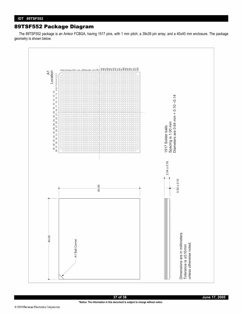
89TSF552 Package DiagramThe 89TSF552 package is an Amkor FCBGA, having 1517 pins, with 1 mm pitch; a 39x39 pin array; and a 40x40 mm enclosure. The package
geometry is shown below.
!
!
"#
# $%
&'%
()
'&*(
$&*
"%'
(& )
(##()
'+'%
*
$#'%
"&,'
(* !
))
-&#'
** $
+.'%
/(*
' &$
+'0
$,"
+($&
1$#
0'%
2"##*
13"
,(&4
(*
))
("
)'+
'%*
"%'
))
5
6
37 of 38 June 17, 2005*Notice: The information in this document is subject to change without notice

IDT 89TSF552
Ordering Information
Valid Combinations
Revision HistoryNovember 24, 2004: Initial publication by IDT.June 17, 2005: Made changes to Tables 21 through 25.
89TSF552BL 1517-pin FCBGA package, Commercial Temperature
NN A AA 5xx AA A
Operating Voltage
DeviceFamily
Product Package Temp range
T
Blank Commercial Temperature(See Thermal Considerations
Traffic Manager
ProductFamily
89 Serial Switching Product
1517-pin FCBGABL
500 Crossbar and scheduler
TM
1.8V ±5% Core Voltage
Detail
552 Queue engine
Switch FabricSF
LegendA = Alpha CharacterN = Numeric Character
section)
38 of 38 June 17, 2005
CORPORATE HEADQUARTERS6024 Silver Creek Valley RoadSan Jose, CA 95138
for SALES:800-345-7015 or 408-284-8200fax: 408-284-2775www.idt.com
for Tech Support:email: [email protected]: 408-284-8208
*Notice: The information in this document is subject to change without notice

Corporate HeadquartersTOYOSU FORESIA, 3-2-24 Toyosu,Koto-ku, Tokyo 135-0061, Japanwww.renesas.com
Contact InformationFor further information on a product, technology, the most up-to-date version of a document, or your nearest sales office, please visit:www.renesas.com/contact/
TrademarksRenesas and the Renesas logo are trademarks of Renesas Electronics Corporation. All trademarks and registered trademarks are the property of their respective owners.
IMPORTANT NOTICE AND DISCLAIMER
RENESAS ELECTRONICS CORPORATION AND ITS SUBSIDIARIES (“RENESAS”) PROVIDES TECHNICAL SPECIFICATIONS AND RELIABILITY DATA (INCLUDING DATASHEETS), DESIGN RESOURCES (INCLUDING REFERENCE DESIGNS), APPLICATION OR OTHER DESIGN ADVICE, WEB TOOLS, SAFETY INFORMATION, AND OTHER RESOURCES “AS IS” AND WITH ALL FAULTS, AND DISCLAIMS ALL WARRANTIES, EXPRESS OR IMPLIED, INCLUDING, WITHOUT LIMITATION, ANY IMPLIED WARRANTIES OF MERCHANTABILITY, FITNESS FOR A PARTICULAR PURPOSE, OR NON-INFRINGEMENT OF THIRD PARTY INTELLECTUAL PROPERTY RIGHTS.
These resources are intended for developers skilled in the art designing with Renesas products. You are solely responsible for (1) selecting the appropriate products for your application, (2) designing, validating, and testing your application, and (3) ensuring your application meets applicable standards, and any other safety, security, or other requirements. These resources are subject to change without notice. Renesas grants you permission to use these resources only for development of an application that uses Renesas products. Other reproduction or use of these resources is strictly prohibited. No license is granted to any other Renesas intellectual property or to any third party intellectual property. Renesas disclaims responsibility for, and you will fully indemnify Renesas and its representatives against, any claims, damages, costs, losses, or liabilities arising out of your use of these resources. Renesas' products are provided only subject to Renesas' Terms and Conditions of Sale or other applicable terms agreed to in writing. No use of any Renesas resources expands or otherwise alters any applicable warranties or warranty disclaimers for these products.
(Rev.1.0 Mar 2020)
© 2020 Renesas Electronics Corporation. All rights reserved.