Embed Size (px)
Citation preview

Dept. of Computers Science and
Engineering, MMU
Microprocessor & its Applications
Prepared by-
Nancy Bindal
Dept. of CSE,
mmu,mullana

Module Contents
The curriculum consists of 5
modules with 8085 as the main
microprocessor
Introduction
8085 pins and their applications
8085 Architecture & Programming
8085 Interfacing Techniques
Introduction to other 8-bit
microprocessors Z80, MC6800
Module I- Introduction
A microprocessor is the main component of a microcomputer system and is also called as CPU (Central Processing Unit). This module is designed to give introduction to some elementary terms related to a microcomputer system. The topics covered are:
Microprocessor as CPU
Hardware and Software
Input & Output Devices
Memories

Module II- 8085 Pins
For complete understanding of the interfacing circuits of memory, I/O devices etc. to the 8085 CPU it is required to learn about the functions of all the pins of 8085. The pins of 8085 are classified in following groups:
Address and Data pins
Control & status pins
Interrupt pins
Serial I/O pins
Clock pins
Reset pins
DMA pins
Power supply pins

Module III- 8085 Architecture
To develop programs for 8085, it is required to completely understand the internal functional blocks of 8085. 8085 architecture includes following functional blocks:
8085 Registers
Timing and control unit
ALU
Interrupt control unit
Serial I/O control unit
Instruction decoder & encoder unit

Module III- Programming the 8085
Programming of 8085 requires
complete knowledge of the
instruction set and its structure. This
requires study of-
8085 Instruction set
8085 addressing modes
One, two & three bytes instruction
Programming examples

Module IV- Interfacing Techniques
A microcomputer system consist of a minimum of
memory & I/O devices. To connect these devices
properly with 8085 is referred to as interfacing. This
module provides interfacing techniques for-
RAM & ROM
I/O devices
Special purpose programmable
devices such as 8255, 8253/8254,
8257, 8259

Module V-Introduction to other 8-bit
microprocessors
This module is designed to develop an introductory knowledge about some other 8-bit microprocessors used in embedded technology. The microprocessors covered in this module are:
Z80 of Zilog
MC6800 of Motorola Corporation

Module I
Introduction: Microcomputer & Microprocessor
A microcomputer is a programmable machine. Modern computers are electronic and digital. The two principal characteristics of a computer are:
It responds to a specific set of instructions in a well-defined manner.
It can execute a prerecorded list of instructions (a program)
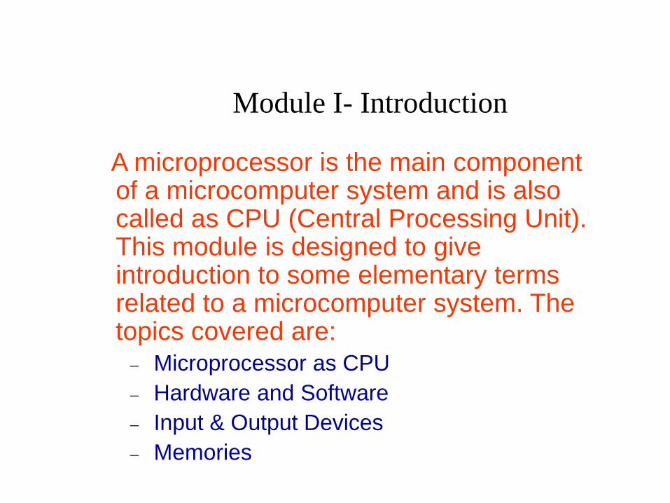
Its main components are CPU
Input & Output devices
memory
A microprocessor is a programmable VLSI chip which controls and performs all operations in a microcomputer. Its main units are-
ALU
Registers
Control Unit
Block diagrams
(Microcomputer & Microprocessor)

Hardware
All general-purpose computers require the following hardware components: Memory: Enables a computer to store data and programs.
Mass storage device: Allows a computer to permanently retain large amounts of data. Common mass storage devices include disk drives and tape drives.
Input device: Usually a keyboard and mouse are the input device through which data and instructions enter a computer.
Output device: A display screen, printer, or other device that lets you see what the computer has accomplished.
Central processing unit (CPU): The heart of the computer, this is the component that actually executes instructions.
Software
The programs and data stored in a microcomputer is called as software.
Programs can be written in low level languages or high level languages.
A low level language can be binary language or assembly language. A CPU recognizes only binary language which is called as
machine language.
Assembly language instructions contain alphabets and/or numeric characters. To run assembly language programs a converter called as assembler is required.
High level languages are more user friendly and contain simple words of English language. To run high level programs, converters such as compilers or interpreters are required.

Input & Output Devices
Input devices are used to input electrical or physical information in a microcomputer system in digital form.
In embedded applications, commonly used input devices are simple switches and sensors.
In general purpose microcomputers, input devices can be keyboards, scanners, mouse etc.
Output devices are used to display or perform required operation.
In embedded applications commonly used output devices are LED display units, LCD display units, stepper motors etc.
In general purpose computers output devices are mainly CRTs, LCD screens, LED screens, Printers etc.

Memories
Memory in a microcomputer system is used to store data and programs temporarily or permanently.
The memories of primary concern for the CPU are only RAM & ROM which are called as primary memory or main memory. The CPU, at any time, only communicates with RAM & ROM.
Other than primary memories, there are also secondary memories which are used for mass storage of data and programs and are transferred to the primary memory when required to be executed by the CPU. Examples of secondary memories are Hard Disks, Floppy Disks, DVDs, flash drives etc.

Memory Classification

Module II-
8085 pins

Pin description
Higher Order Address pins- A15 –A8
Lower Order Address/ Data Pins- AD7-AD0
These are time multiplexed pins and are de-multiplexed using the pin ALE
Control Pins – RD, WR
These are active low Read & Write pins
Status Pins –ALE, IO/M (active low), S1, S0
ALE (Address Latch Enable)-Used to de-multiplex AD7-AD0
IO/M – Used to select I/O or Memory operation
S1,S0 – Denote the status of data on data bus
Interrupt Pins – TRAP, RST7.5, RST 6.5, RST 5.5, INTR, INTA
These are hardware interrupts used to initiate an interrupt service routine stored at predefined locations of the system memory.
Serial I/O pins – SID (Serial Input Data), SOD (Serial Output Data)
These pins are used to interface 8085 with a serial device.

Pin Description Contd.
Clock Pins- X1, X2, CLK(OUT) X1, X2- These are clock input pins. A crystal is connected between
these pins such that fcrystal= 2f8085 where fcrystal= crystal frequency & f8085 = operating frequency of 8085
CLK(OUT) – This is an auxiliary clock output source
Reset Pins – Reset In (active low), Reset Out Reset In is used to reset 8085 whereas Reset Out can be used to
reset other devices in the system
DMA (Direct Memory Access) pins – HOLD, HLDA These pins are used when data transfer is to be performed directly
between an external device and the main memory of the system.
Power Supply Pins - +VCC, VSS

Module III –
8085 Architecture

8085 Architecture Contd..
The Registers are of 8-bit & 16-bit size used for different purposes
A- Accumulator – This is an special purpose register. All the ALU operations are performed with reference to the
contents of Accumulator.
B,C,D,E,H,L – General purpose registers. These registers can also be used for 16-bit operations in pairs. The default
pairs are BC, DE & HL.
F – Flag register – This register indicates the status of the ALU operation.
PC – Program Counter – This is a 16-bit register used to address the memory location from where an
instruction is going to be executed.
SP – Stack pointer - This is a 16-bit register used to address the top of the stack memory location.
Temporary register, W & Z – These registers are only used by 8085 and are not available for the
programmer.

8085 Architecture Contd..
ALU –Arithmetic & Logic Unit
ALU of 8085 performs 8-bit arithmetic & logical operations. The operations are generally performed with Accumulator as one of the operands. The result is saved in accumulator register.
Timing & Control Unit
This unit works as the brain of the CPU and generates all the timing and control signals to perform all the internal & external operations of the CPU.
Instruction Decoder & Machine Cycle Encoder Unit This unit decodes the op-code stored in the Instruction Register (IR) and
encodes it for the timing & control unit to perform the execution of the instruction.
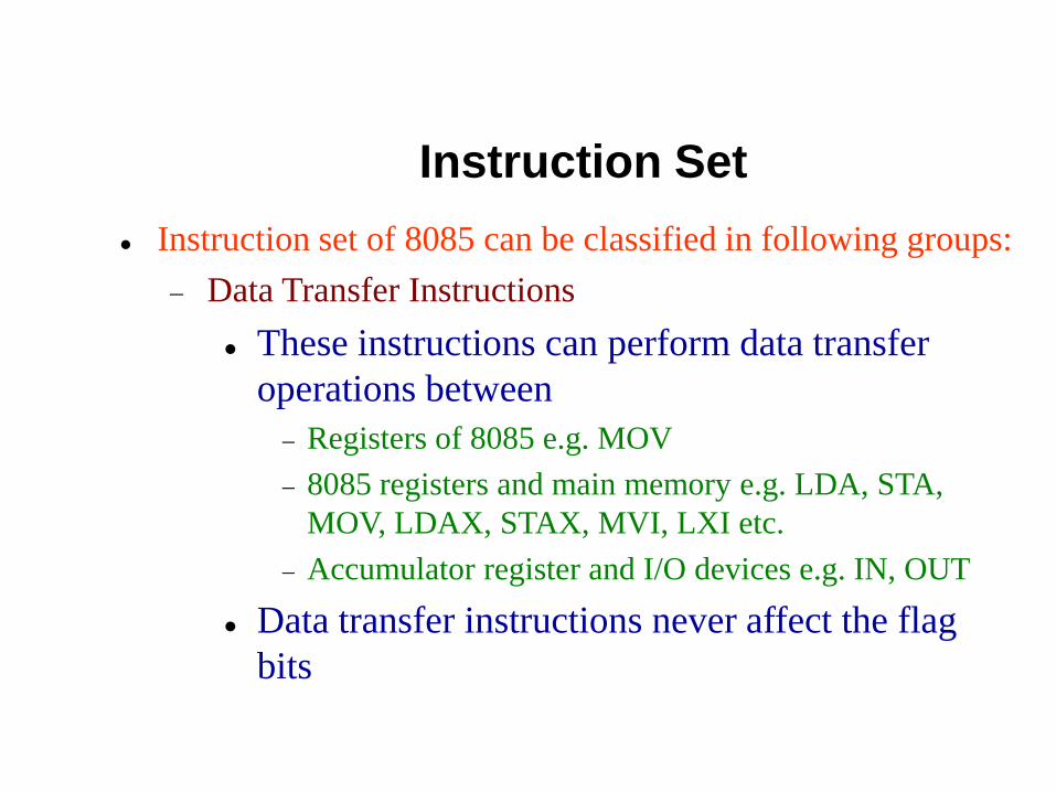
Instruction Set
Instruction set of 8085 can be classified in following groups:
Data Transfer Instructions
These instructions can perform data transfer
operations between
Registers of 8085 e.g. MOV
8085 registers and main memory e.g. LDA, STA,
MOV, LDAX, STAX, MVI, LXI etc.
Accumulator register and I/O devices e.g. IN, OUT
Data transfer instructions never affect the flag
bits

Instruction Set Contd..
Arithmetic Instructions
8085 can perform only 8-bit addition, subtraction and compare operations. These operations are always performed with accumulator as one of the operands. The status of the result can be verified by the contents of the flag register.
Op-codes for arithmetic instructions include ADD, ADI, ADC, ACI, SUB, SUI, SBB, SBI, CMP, CPI
Logical Instructions
8085 can perform 8-bit basic logical operations -AND, OR, XOR, NOT with some special operations such as rotate and shift operations
Logical instructions also modify the flag bits.
Op-codes for logical instructions include ANA, ANI, ORA, ORI, XRA, XRI, CMA, RAL, RLC, RAR, RRC etc.

Instruction Set Contd..
Program Control Instructions These instructions are used to transfer the program
control: to jump from one memory location to any other memory
location within a program
from one program to another program called as a subroutine
8085 Instruction set consists of following program control instructions:
Jump Instructions
Call & Return Instructions
Restart instructions

Instruction Set Contd..
Program control instructions
Unconditional or Conditional
Unconditional program control instructions perform
branching operation unconditionally
Conditional program control instructions perform
branching operation with reference to the condition
of flag bits.

Instruction Set Contd..
Unconditional Program control instructions are
JMP
Call & RET
RST n (n=0-7)
Conditional Program control instructions are JNC, JC, JNZ, JZ, JP, JM, JPE, JPO
CNC, CC, CNZ, CZ, CP, CM, CPE, CPO
RNC, RC, RNZ, RZ, RP, RM, RPE, RPO
Instruction Set Contd..
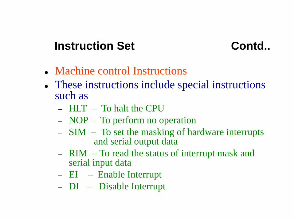
Machine control Instructions
These instructions include special instructions such as HLT – To halt the CPU
NOP – To perform no operation
SIM – To set the masking of hardware interrupts and serial output data
RIM – To read the status of interrupt mask and serial input data
EI – Enable Interrupt
DI – Disable Interrupt
Programming of 8085
The following link can be used to access different type of programs.
Lab Manual
The programs can be loaded and verified in the 8085 based microcomputer system available in the microprocessor lab

Addressing Modes
8085 instructions can be classified in following addressing modes Register Addressing mode
Instructions which have their operands in registers only e.g. MOV, ADD, SUB, ANA, ORA, XRA etc.
Immediate Addressing mode Instructions in which operand immediately follows the
op-code e.g. MVI, LXI, ADI, SUI, ANI, ORI etc.
Direct Addressing mode Instructions have their operands in memory and the
16-bit memory address is specified in the instruction e.g. LDA, STA, LHLD, SHLD etc.
Addressing Modes Contd..
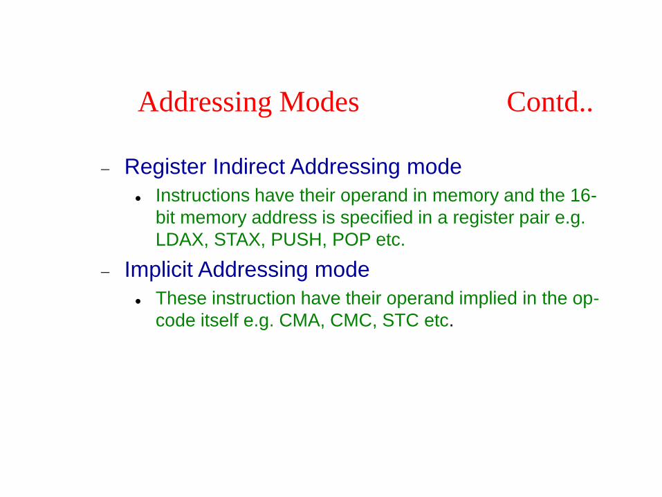
Register Indirect Addressing mode
Instructions have their operand in memory and the 16-
bit memory address is specified in a register pair e.g.
LDAX, STAX, PUSH, POP etc.
Implicit Addressing mode
These instruction have their operand implied in the op-
code itself e.g. CMA, CMC, STC etc.

Instruction size
An instruction is assembled in the memory of a microcomputer system in binary form. The size of an instruction signifies how much memory space is required to load an instruction in the memory. 8085 instructions are of following sizes:
One-byte Instructions
e.g. MOV, ADD, ANA, SUB, ORA etc.
Two-byte instructions
e.g. MVI, ADI, ANI, ORI, XRI etc.
Three-byte instructions
e.g. LXI, LDA, STA, LHLD, SHLD etc.

Module IV:Interfacing Techniques
Memory Interfacing
8085 uses 16-bit memory addressing system allowing
a maximum of 64 KB size of memory
The logical memory address range is 0000h-FFFFh
These 64k addresses can be allotted separately to
RAMs & ROMs
Some interfacing circuit examples can be found in the
following link
Interfacing Examples

Interfacing Contd..
I/O Interfacing
To interface Input Devices Octal buffers are used. These octal buffers are called as input ports
Octal buffers contain a set of eight buffers for an 8-bit system data bus
A buffer is basically a current amplifier which amplifies the smaller magnitude currents of input devices before being supplied to the CPU
The tri-state logic also provides the addressing and control logic for the CPU

Interfacing Contd..
To interface output devices Octal Latches are used.
A latch is basically a D Flip-Flop
Latches are used to hold the output data because information on system data bus is available for a very small duration of time.
I/O interfacing techniques

I/O structure of 8085

Interfacing Contd..
There are three major types of data transfer between the microcomputer and art I/O device. They are- Programmed I/O : In programmed I/O the data
transfer is accomplished through an I/O port and controlled by software.
Interrupt driven I/O : In interrupt driven I/O, the I/O device will interrupt the processor, and initiate data transfer.
Direct memory access (DMA) : In DMA, the data transfer between memory and I/O can be performed by bypassing the microprocessor.

Interfacing Contd..
Some special purpose programmable
devices used with 8085 are listed in the
table of next slide.
These devices are used in the system
according to the requirement.

Interfacing Contd..

Interfacing Contd..