Embed Size (px)
Citation preview
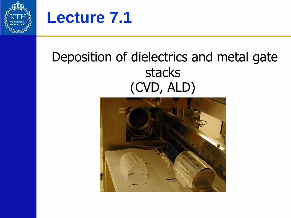
Deposition of dielectrics and metal gate stacks
(CVD, ALD)
Lecture 7.1
IH2655 Spring 2010
Mikael Östling 2
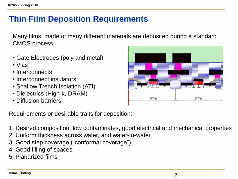
Thin Film Deposition Requirements
Requirements or desirable traits for deposition:
1. Desired composition, low contaminates, good electrical and mechanical properties
2. Uniform thickness across wafer, and wafer-to-wafer
3. Good step coverage (“conformal coverage”)
4. Good filling of spaces
5. Planarized films
Many films, made of many different materials are deposited during a standard
CMOS process.
• Gate Electrodes (poly and metal)
• Vias
• Interconnects
• Interconnect insulators
• Shallow Trench Isolation (ATI)
• Dielectrics (High-k, DRAM)
• Diffusion barriers
IH2655 Spring 2010
Mikael Östling
Many films, made of many different materials are deposited during a standard
CMOS process.
• Gate Electrodes (poly and metal)
• Vias
• Interconnects
• Interconnect insulators
• Shallow Trench Isolation (ATI)
• Dielectrics (High-k, DRAM)
• Diffusion barriers
3
Thin Film Deposition Requirements
Requirements or desirable traits for deposition:
1. Desired composition, low contaminates, good electrical and mechanical properties
2. Uniform thickness across wafer, and wafer-to-wafer
3. Good step coverage (“conformal coverage”)
4. Good filling of spaces
5. Planarized films
IH2655 Spring 2010
Mikael Östling 4
• Chemical Vapor Deposition (CVD) • Basic definitions
• Reactor designs
• Examples • Polysilicon CVD
• Silicon Dioxide CVD
• Silicon Nitride CVD
• Modeling
• Atomic Layer Deposition (ALD) • Basic Definitions
• Reactor Designs
• Example • Aluminum Oxide ALD
CVD and ALD of polysilicon and dielectric thin films
IH2655 Spring 2010
Mikael Östling
Chemical vapor deposition (CVD) - Definition
Constituents of the films are delivered through the gas phase. For CVD
reactant gases are introduced into the deposition chamber and chemical
reactions are used to deposit a thin film on the wafer surface.
Energy for this reaction can origin from heat, radiation or from a plasma.
Typical pressure range: 0.01 to 1 bar
Good film quality and step coverage.
IH2655 Spring 2010
Mikael Östling 6
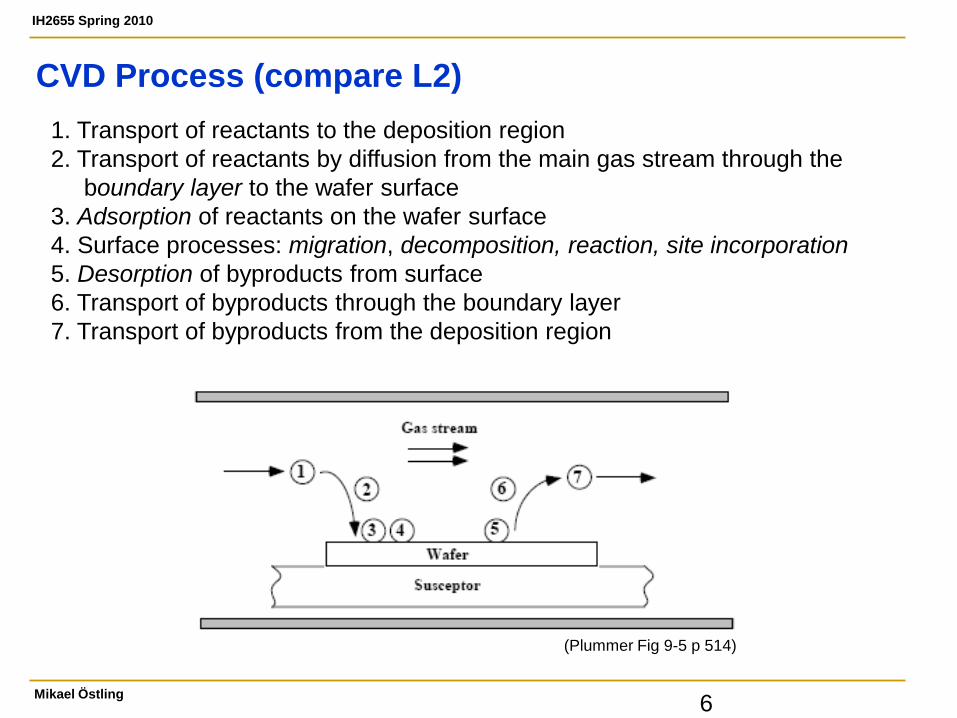
(Plummer Fig 9-5 p 514)
1. Transport of reactants to the deposition region
2. Transport of reactants by diffusion from the main gas stream through the
boundary layer to the wafer surface
3. Adsorption of reactants on the wafer surface
4. Surface processes: migration, decomposition, reaction, site incorporation
5. Desorption of byproducts from surface
6. Transport of byproducts through the boundary layer
7. Transport of byproducts from the deposition region
CVD Process (compare L2)
IH2655 Spring 2010
Mikael Östling 7
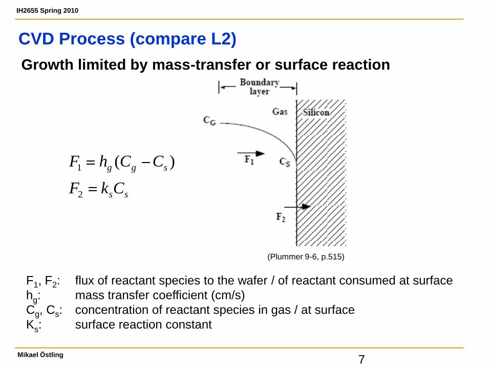
Growth limited by mass-transfer or surface reaction
(Plummer 9-6, p.515)
F1, F2: flux of reactant species to the wafer / of reactant consumed at surface
hg: mass transfer coefficient (cm/s)
Cg, Cs: concentration of reactant species in gas / at surface
Ks: surface reaction constant
ss
sgg
CkF
CChF
2
1 )(
CVD Process (compare L2)
IH2655 Spring 2010
Mikael Östling 8
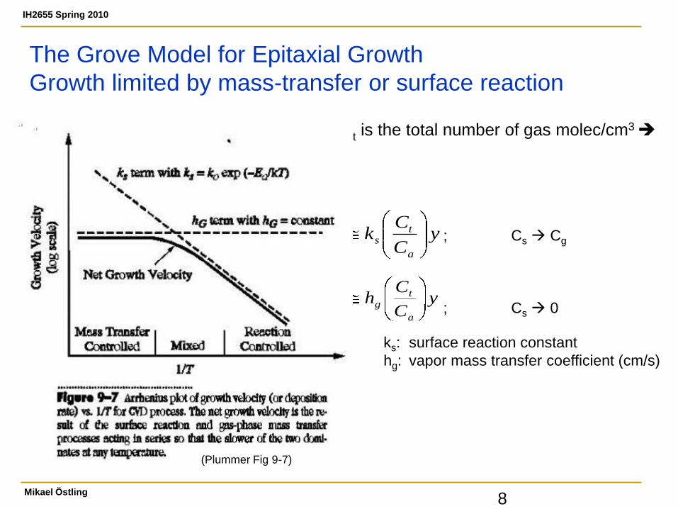
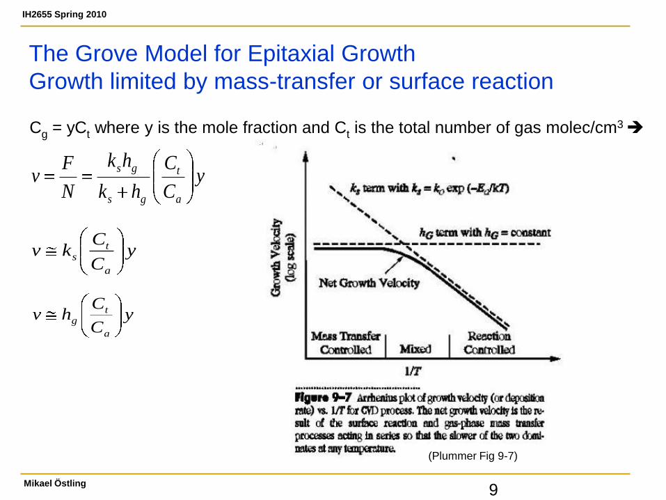
The Grove Model for Epitaxial Growth
Growth limited by mass-transfer or surface reaction
Cg = yCt where y is the mole fraction and Ct is the total number of gas molec/cm3
ks small Surface reaction controlled ; Cs Cg
hg small Mass-transport controlled ; Cs 0
yC
Ckv
a
ts
yC
Chv
a
tg
ks: surface reaction constant
hg: vapor mass transfer coefficient (cm/s)
yC
C
hk
hk
N
Fv
a
t
gs
gs
(Plummer Fig 9-7)
IH2655 Spring 2010
Mikael Östling 9
The Grove Model for Epitaxial Growth
Growth limited by mass-transfer or surface reaction
Cg = yCt where y is the mole fraction and Ct is the total number of gas molec/cm3
yC
Ckv
a
ts
yC
Chv
a
tg
yC
C
hk
hk
N
Fv
a
t
gs
gs
(Plummer Fig 9-7)
IH2655 Spring 2010
Mikael Östling
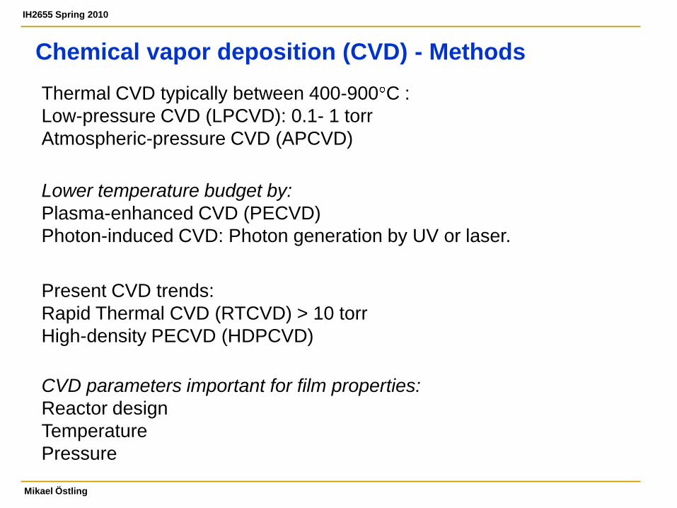
Chemical vapor deposition (CVD) - Methods
Thermal CVD typically between 400-900 C :
Low-pressure CVD (LPCVD): 0.1- 1 torr
Atmospheric-pressure CVD (APCVD)
Lower temperature budget by:
Plasma-enhanced CVD (PECVD)
Photon-induced CVD: Photon generation by UV or laser.
Present CVD trends:
Rapid Thermal CVD (RTCVD) > 10 torr
High-density PECVD (HDPCVD)
CVD parameters important for film properties:
Reactor design
Temperature
Pressure
IH2655 Spring 2010
Mikael Östling 11
Increased Increased
supersaturation temperature
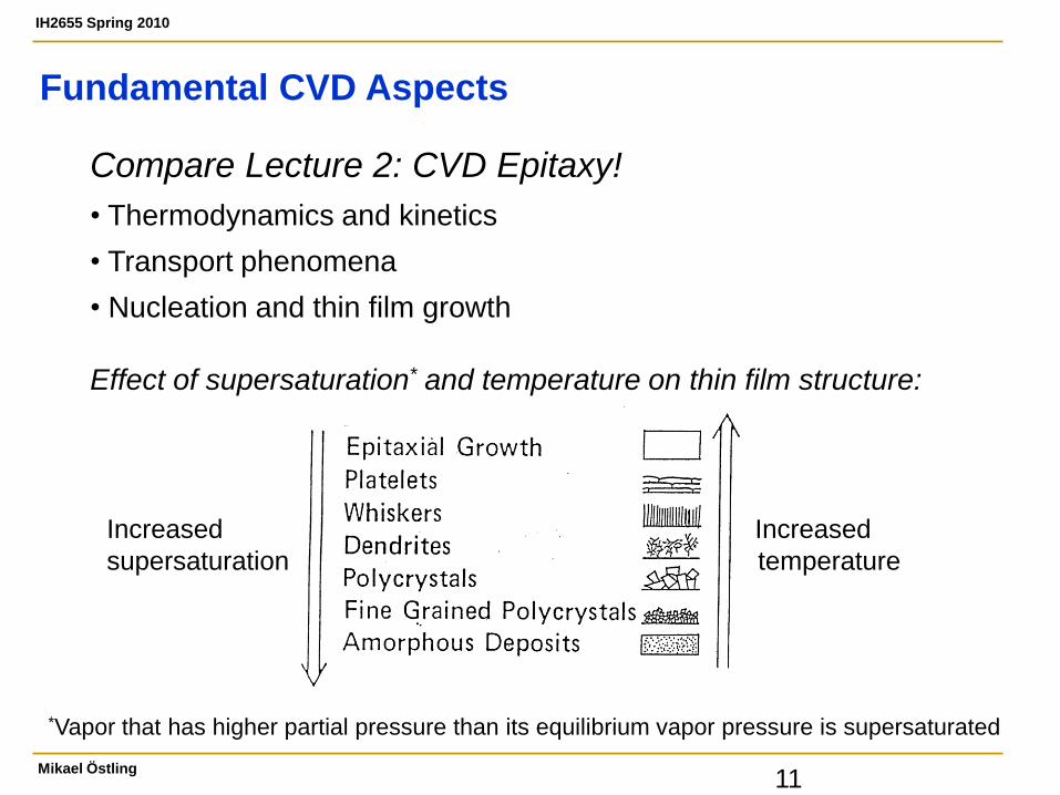
Fundamental CVD Aspects
Compare Lecture 2: CVD Epitaxy!
• Thermodynamics and kinetics
• Transport phenomena
• Nucleation and thin film growth
Effect of supersaturation* and temperature on thin film structure:
*Vapor that has higher partial pressure than its equilibrium vapor pressure is supersaturated
IH2655 Spring 2010
Mikael Östling 12
• Chemical Vapor Deposition (CVD) • Basic definitions
• Reactor designs
• Examples • Polysilicon CVD
• Silicon Dioxide CVD
• Silicon Nitride CVD
• Modeling
• Atomic Layer Deposition (ALD) • Basic Definitions
• Reactor Designs
• Example • Aluminum Oxide ALD
CVD and ALD of polysilicon and dielectric thin films
IH2655 Spring 2010
Mikael Östling
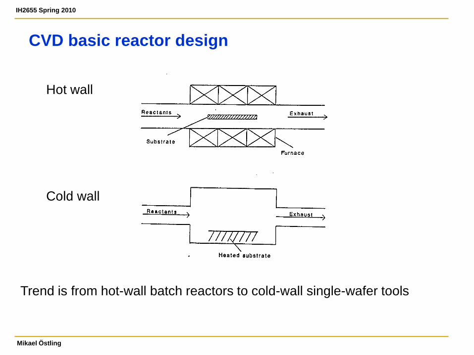
CVD basic reactor design
Hot wall
Cold wall
Trend is from hot-wall batch reactors to cold-wall single-wafer tools
IH2655 Spring 2010
Mikael Östling
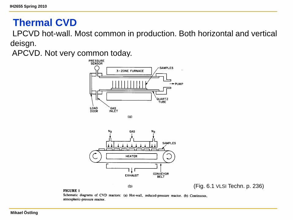
Thermal CVD LPCVD hot-wall. Most common in production. Both horizontal and vertical
deisgn.
APCVD. Not very common today.
(Fig. 6.1 VLSI Techn. p. 236)
IH2655 Spring 2010
Mikael Östling
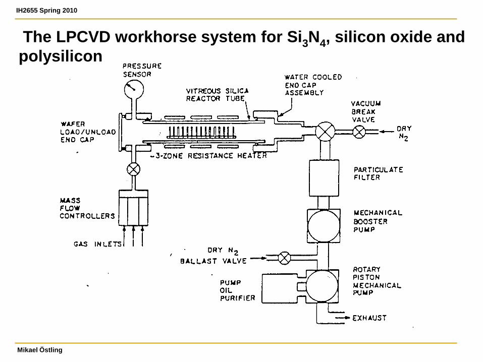
The LPCVD workhorse system for Si3N4, silicon oxide and
polysilicon
IH2655 Spring 2010
Mikael Östling 16
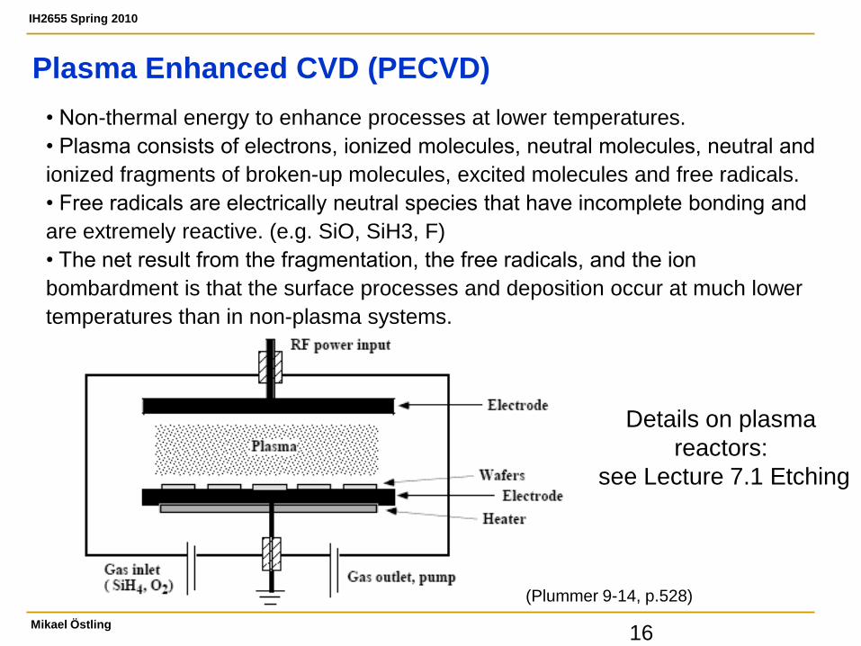
Plasma Enhanced CVD (PECVD)
(Plummer 9-14, p.528)
• Non-thermal energy to enhance processes at lower temperatures.
• Plasma consists of electrons, ionized molecules, neutral molecules, neutral and
ionized fragments of broken-up molecules, excited molecules and free radicals.
• Free radicals are electrically neutral species that have incomplete bonding and
are extremely reactive. (e.g. SiO, SiH3, F)
• The net result from the fragmentation, the free radicals, and the ion
bombardment is that the surface processes and deposition occur at much lower
temperatures than in non-plasma systems.
Details on plasma
reactors:
see Lecture 7.1 Etching
IH2655 SPRING 2009
Mikael Östling KTH 17
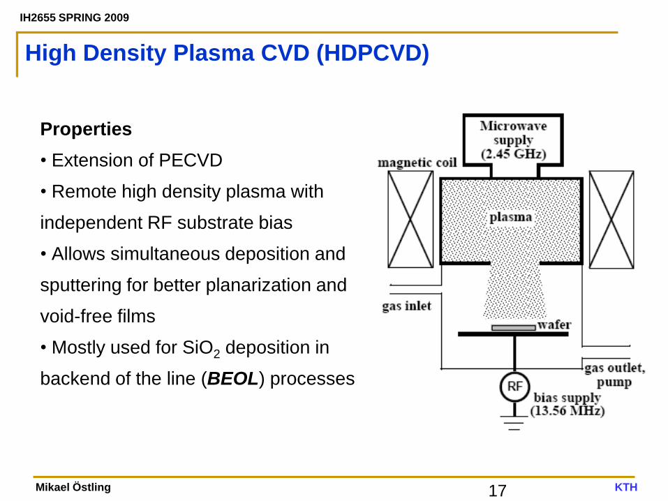
High Density Plasma CVD (HDPCVD)
Properties
• Extension of PECVD
• Remote high density plasma with
independent RF substrate bias
• Allows simultaneous deposition and
sputtering for better planarization and
void-free films
• Mostly used for SiO2 deposition in
backend of the line (BEOL) processes
IH2655 Spring 2010
Mikael Östling
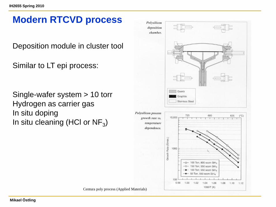
Centura poly process (Applied Materials)
Modern RTCVD process
Deposition module in cluster tool
Similar to LT epi process:
Single-wafer system > 10 torr
Hydrogen as carrier gas
In situ doping
In situ cleaning (HCl or NF3)
IH2655 Spring 2010
Mikael Östling
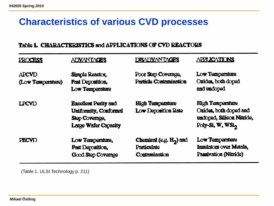
Characteristics of various CVD processes
(Table 1. ULSI Technology p. 211)
IH2655 Spring 2010
Mikael Östling 20
• Chemical Vapor Deposition (CVD) • Basic definitions
• Reactor designs
• Examples • Polysilicon CVD
• Silicon Dioxide CVD
• Silicon Nitride CVD
• Modeling
• Atomic Layer Deposition (ALD) • Basic Definitions
• Reactor Designs
• Example • Aluminum Oxide ALD
CVD and ALD of polysilicon and dielectric thin films
IH2655 Spring 2010
Mikael Östling
Polysilicon
Used in VLSI for:
n+ or p+ gate electrode material in CMOS (see below)
n+ emitter contact in BIP (see below), so-called polysilicon emitter technology
Diffusion source (double-poly bipolar process for formation of E and B)
(see below)
Local interconnects
Deep-trench filling (see below)
Resistances
Also poly-SiGe of interest as common p+-gate electrode in CMOS
(so-called mid bandgap material)
IH2655 Spring 2010
Mikael Östling 22
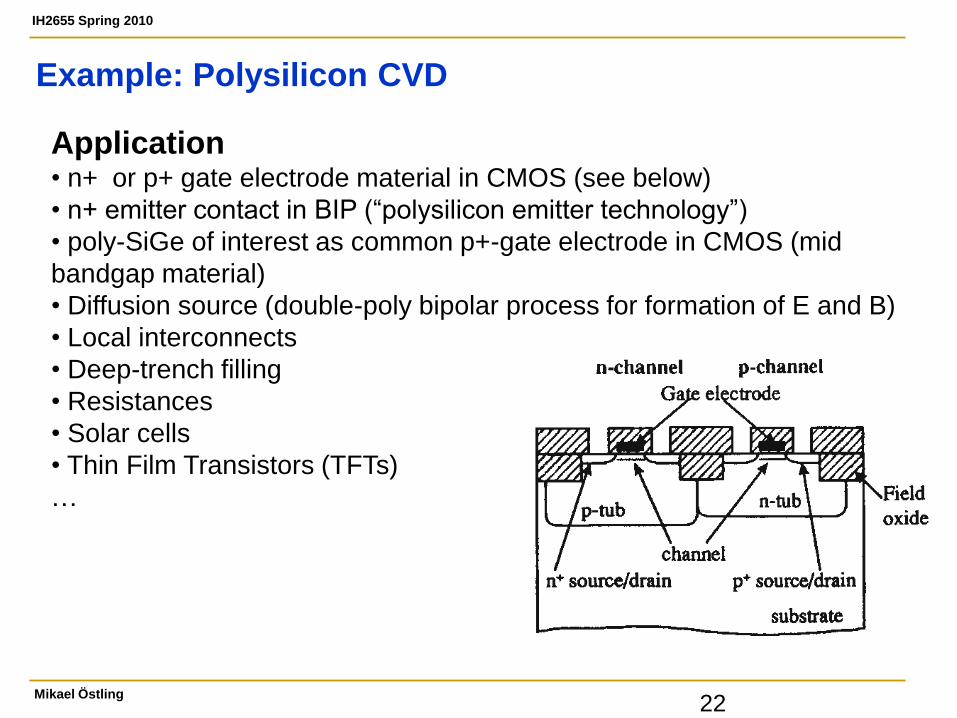
Example: Polysilicon CVD
Application • n+ or p+ gate electrode material in CMOS (see below)
• n+ emitter contact in BIP (“polysilicon emitter technology”)
• poly-SiGe of interest as common p+-gate electrode in CMOS (mid
bandgap material)
• Diffusion source (double-poly bipolar process for formation of E and B)
• Local interconnects
• Deep-trench filling
• Resistances
• Solar cells
• Thin Film Transistors (TFTs)
…
IH2655 Spring 2010
Mikael Östling
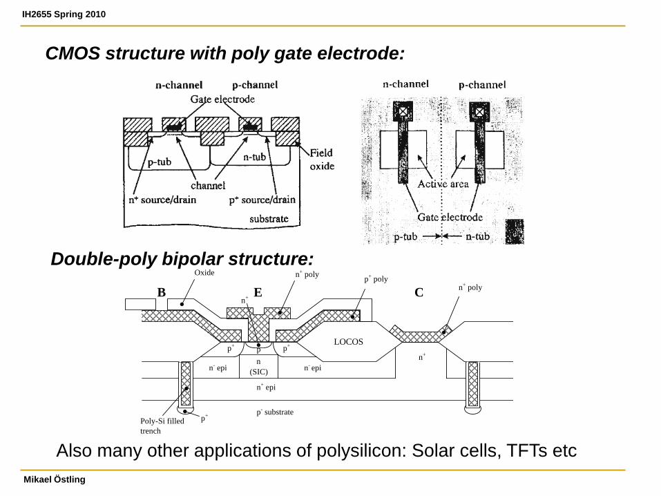
p- substrate
p
p+
n
n+ epi
p+
n+
LOCOS
E B C
n+ poly
n+ poly p+ poly
Oxide
Poly-Si filled
trench
n+
p+
n- epi
n- epi
(SIC)
Double-poly bipolar structure:
Also many other applications of polysilicon: Solar cells, TFTs etc
CMOS structure with poly gate electrode:
IH2655 Spring 2010
Mikael Östling
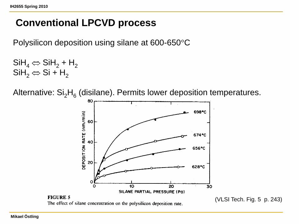
Conventional LPCVD process
Polysilicon deposition using silane at 600-650 C
SiH4 SiH2 + H2
SiH2 Si + H2
Alternative: Si2H6 (disilane). Permits lower deposition temperatures.
(VLSI Tech. Fig. 5 p. 243)
IH2655 Spring 2010
Mikael Östling
Arrhenius plot of SiH4 deposition at different partial
pressures of SiH4
Activation energy of 1.7 eV
(VLSI Tech. Fig. 5 p. 240)
IH2655 Spring 2010
Mikael Östling
Exact microstructure depends on a
number of factors:
Pressure, dopants, temperature,
thickness, recrystallization etc
Grain growth important for final
electrical properties
Microstructure of polysilicon
T > 625 C Columnar growth.
Preferential (110) orient.
T < 575 C Amorphous
T ~ 600 C Microcrystalline
polysilicon
Growth and Physical Properties of I.PCVD Polycrystalline Silicon
Films, G. Harbeke, SOLID-STATE SCIENCE AND TECHNOLOGY 1984
Preferably crystallize
in (111) orientation
IH2655 SPRING 2009
Mikael Östling KTH 27
Temperature and Pressure Dependence
- grain size >> functional structure
- surface roughness complicates etch stop
Poly-Silicon:
620 °C
160 mTorr
-Silicon:
580 °C
400 mTorr
+ smooth surface
- gas phase nucleation
- recrystalization after annealing
Example: Polysilicon CVD
IH2655 Spring 2010
Mikael Östling
Exact microstructure depends on a
number of factors:
Pressure, dopants, temperature,
thickness, recrystallization etc
Grain growth important for final
electrical properties
(Plummer Fig 9-32 p.
560)
Microstructure of polysilicon
T > 625 C Columnar growth.
Preferential (110) orient.
T < 575 C Amorphous
T ~ 600 C Microcrystalline
polysilicon
IH2655 Spring 2010
Mikael Östling
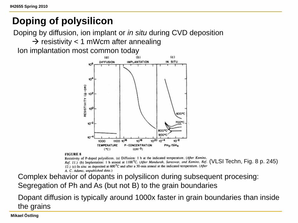
Doping by diffusion, ion implant or in situ during CVD deposition
resistivity < 1 mWcm after annealing
Ion implantation most common today
(VLSI Techn, Fig. 8 p. 245)
Dopant diffusion is typically around 1000x faster in grain boundaries than inside
the grains
Doping of polysilicon
Complex behavior of dopants in polysilicon during subsequent procesing:
Segregation of Ph and As (but not B) to the grain boundaries
IH2655 Spring 2010
Mikael Östling
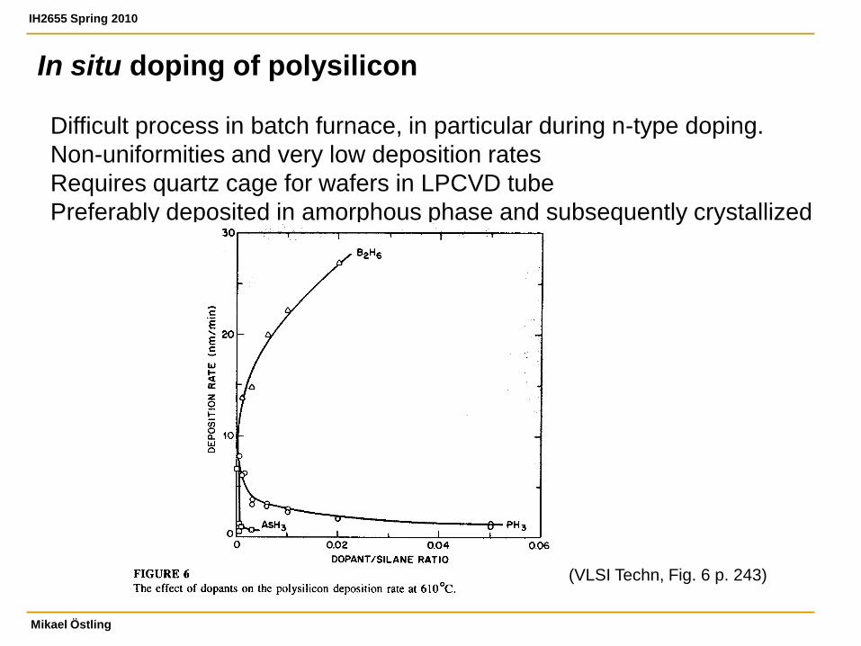
In situ doping of polysilicon
Difficult process in batch furnace, in particular during n-type doping.
Non-uniformities and very low deposition rates
Requires quartz cage for wafers in LPCVD tube
Preferably deposited in amorphous phase and subsequently crystallized
(VLSI Techn, Fig. 6 p. 243)
IH2655 Spring 2010
Mikael Östling 31
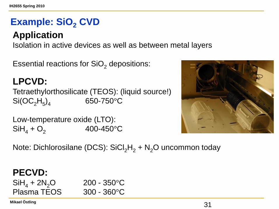
Application Isolation in active devices as well as between metal layers
Essential reactions for SiO2 depositions:
LPCVD: Tetraethylorthosilicate (TEOS): (liquid source!)
Si(OC2H5)4 650-750 C
Low-temperature oxide (LTO):
SiH4 + O2 400-450 C
Note: Dichlorosilane (DCS): SiCl2H2 + N2O uncommon today
PECVD:
SiH4 + 2N2O 200 - 350 C
Plasma TEOS 300 - 360 C
Example: SiO2 CVD
IH2655 Spring 2010
Mikael Östling
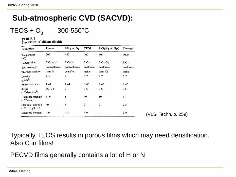
Sub-atmospheric CVD (SACVD):
TEOS + O3 300-550 C
Typically TEOS results in porous films which may need densification.
Also C in films!
PECVD films generally contains a lot of H or N
(VLSI Techn. p. 259)
IH2655 Spring 2010
Mikael Östling
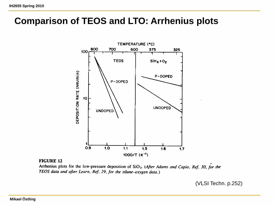
Comparison of TEOS and LTO: Arrhenius plots
(VLSI Techn. p.252)
IH2655 Spring 2010
Mikael Östling 34
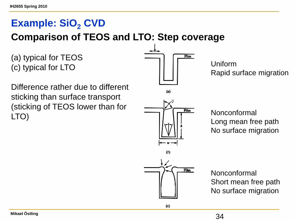
Comparison of TEOS and LTO: Step coverage
(a) typical for TEOS
(c) typical for LTO
Difference rather due to different
sticking than surface transport
(sticking of TEOS lower than for
LTO)
Example: SiO2 CVD
Uniform
Rapid surface migration
Nonconformal
Long mean free path
No surface migration
Nonconformal
Short mean free path
No surface migration
IH2655 Spring 2010
Mikael Östling 35
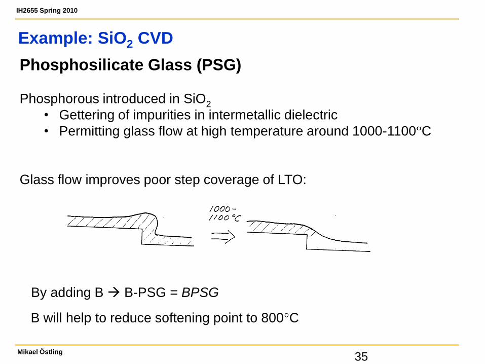
Phosphosilicate Glass (PSG)
Phosphorous introduced in SiO2
• Gettering of impurities in intermetallic dielectric
• Permitting glass flow at high temperature around 1000-1100 C
Glass flow improves poor step coverage of LTO:
By adding B B-PSG = BPSG
B will help to reduce softening point to 800 C
Example: SiO2 CVD
IH2655 Spring 2010
Mikael Östling
Silicon nitride Applications:
For mask in LOCOS process (barrier against oxygen diffusion)
Passivation layer: (barrier against H2O, sodium)
LPCVD 3SiH2Cl2 + 4NH3 Si3N4 + 6 HCl + 6H2 650-800 C
(most common)
3SiH4 + 4NH3 Si3N4 + 12H2 700-900 C
Excess of NH3 used in reaction!
PECVD Si3N4 used for passivation using silane and NH3 at 200-400 C
Contains much H! Usually non-stoichiometric!
Stress can be tuned by plasma parameters
New trend: High-density plasma systems
IH2655 Spring 2010
Mikael Östling
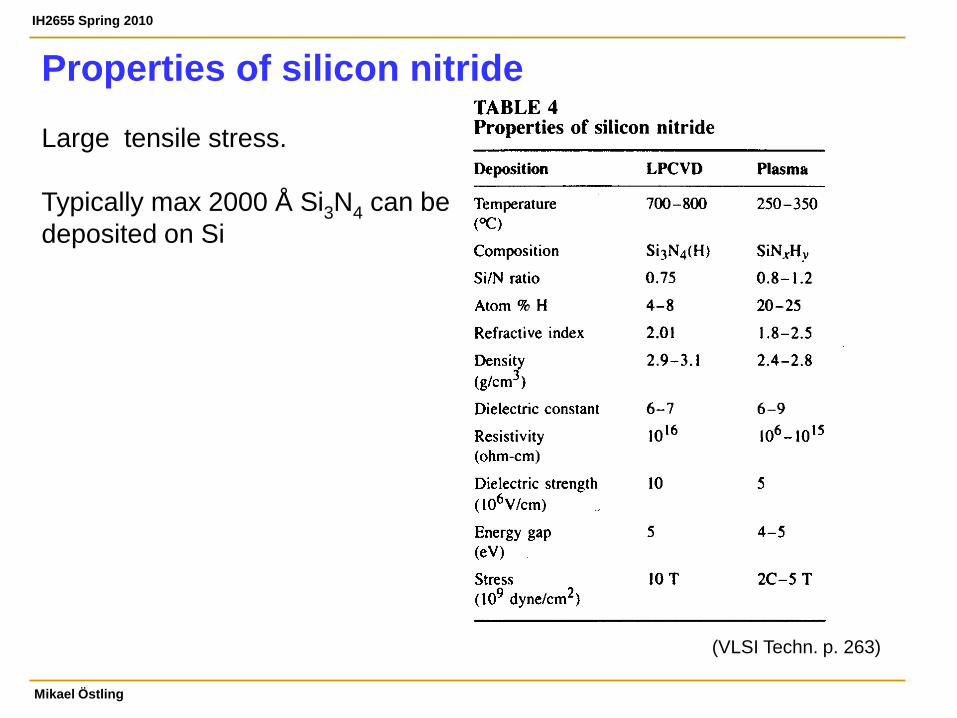
Properties of silicon nitride
Large tensile stress.
Typically max 2000 Å Si3N4 can be
deposited on Si
(VLSI Techn. p. 263)
IH2655 Spring 2010
Mikael Östling 38
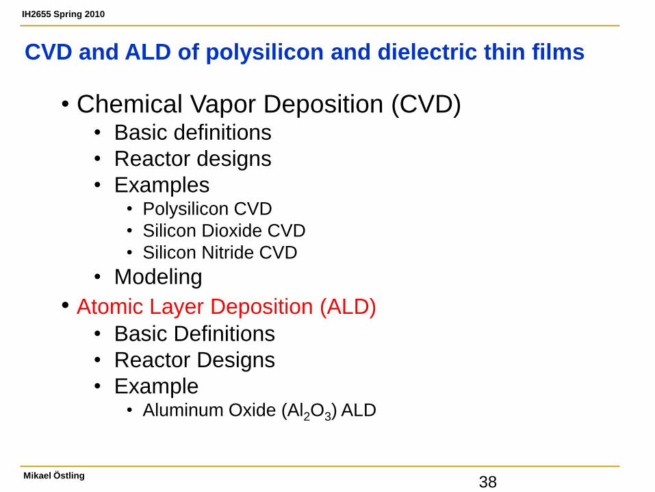
• Chemical Vapor Deposition (CVD) • Basic definitions
• Reactor designs
• Examples • Polysilicon CVD
• Silicon Dioxide CVD
• Silicon Nitride CVD
• Modeling
• Atomic Layer Deposition (ALD)
• Basic Definitions
• Reactor Designs
• Example • Aluminum Oxide (Al2O3) ALD
CVD and ALD of polysilicon and dielectric thin films
IH2655 SPRING 2009
Mikael Östling KTH 39
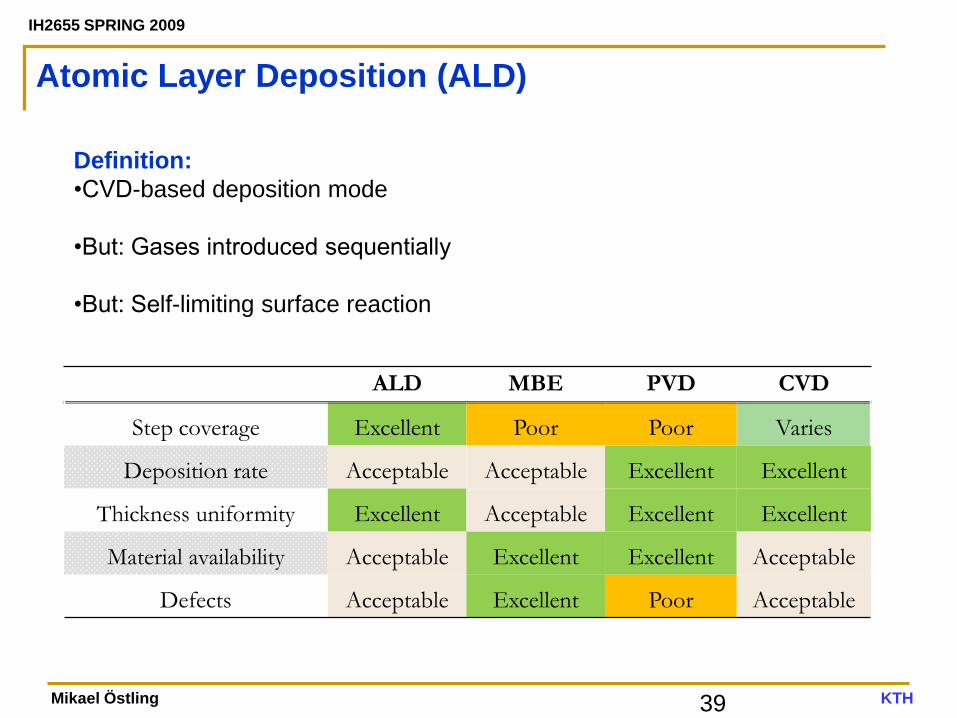
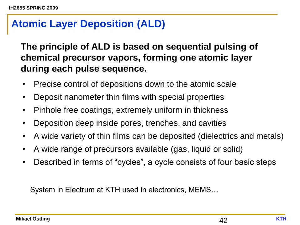
Atomic Layer Deposition (ALD)
Definition:
•CVD-based deposition mode
•But: Gases introduced sequentially
•But: Self-limiting surface reaction
ALD MBE PVD CVD
Step coverage Excellent Poor Poor Varies
Deposition rate Acceptable Acceptable Excellent Excellent
Thickness uniformity Excellent Acceptable Excellent Excellent
Material availability Acceptable Excellent Excellent Acceptable
Defects Acceptable Excellent Poor Acceptable
IH2655 SPRING 2009
Mikael Östling KTH 40
Atomic Layer Deposition (ALD)
Definition:
•CVD-based deposition mode
•But: Gases introduced sequentially
•But: Self-limiting surface reaction
Application:
•Thin films from 1-500 nm
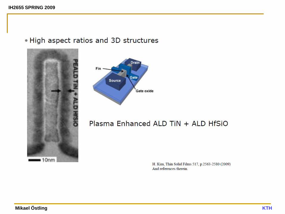
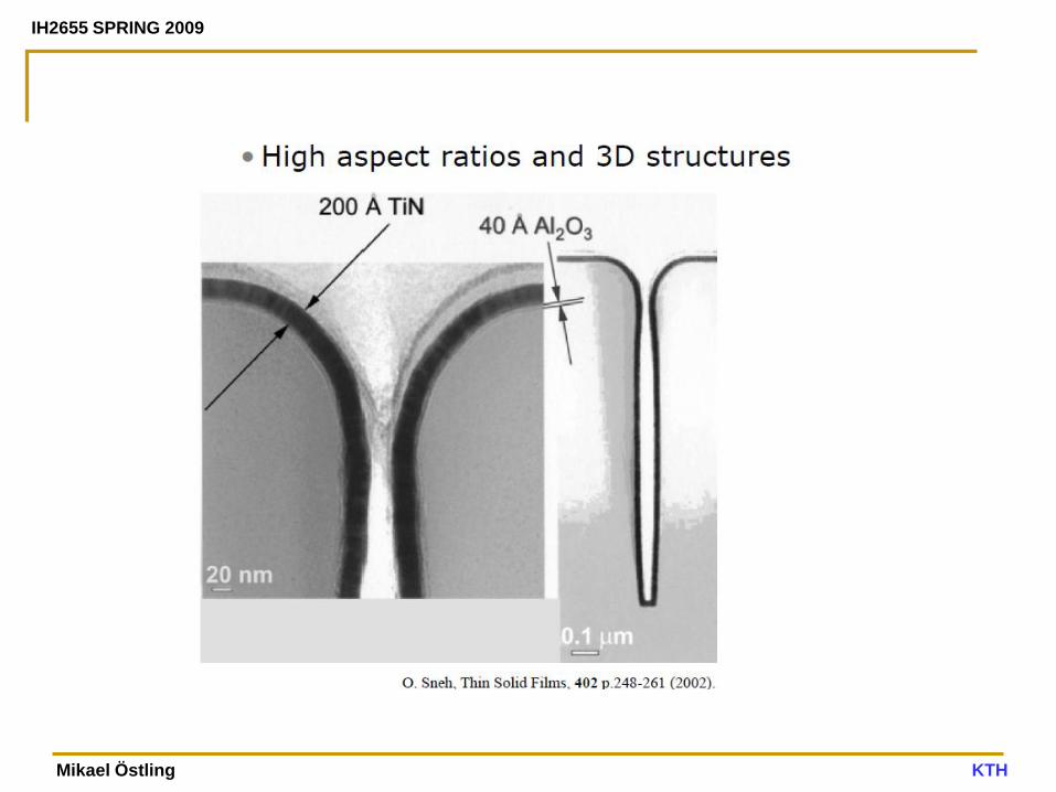
•High aspect / 3D structures
•Good film quality
•Most viable sub-5 nm deposition technique
IH2655 SPRING 2009
Mikael Östling KTH
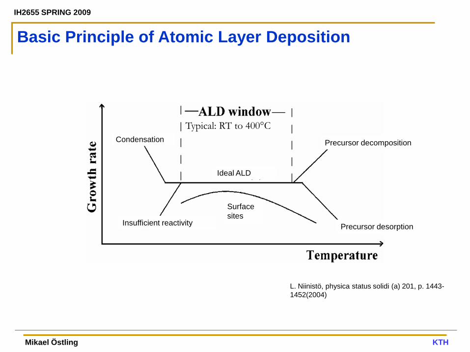
L. Niinistö, physica status solidi (a) 201, p. 1443-
1452(2004)
Precursor desorption
Precursor decomposition
Typical: RT to 400°C
Ideal ALD
Surface
sites
Condensation
Insufficient reactivity
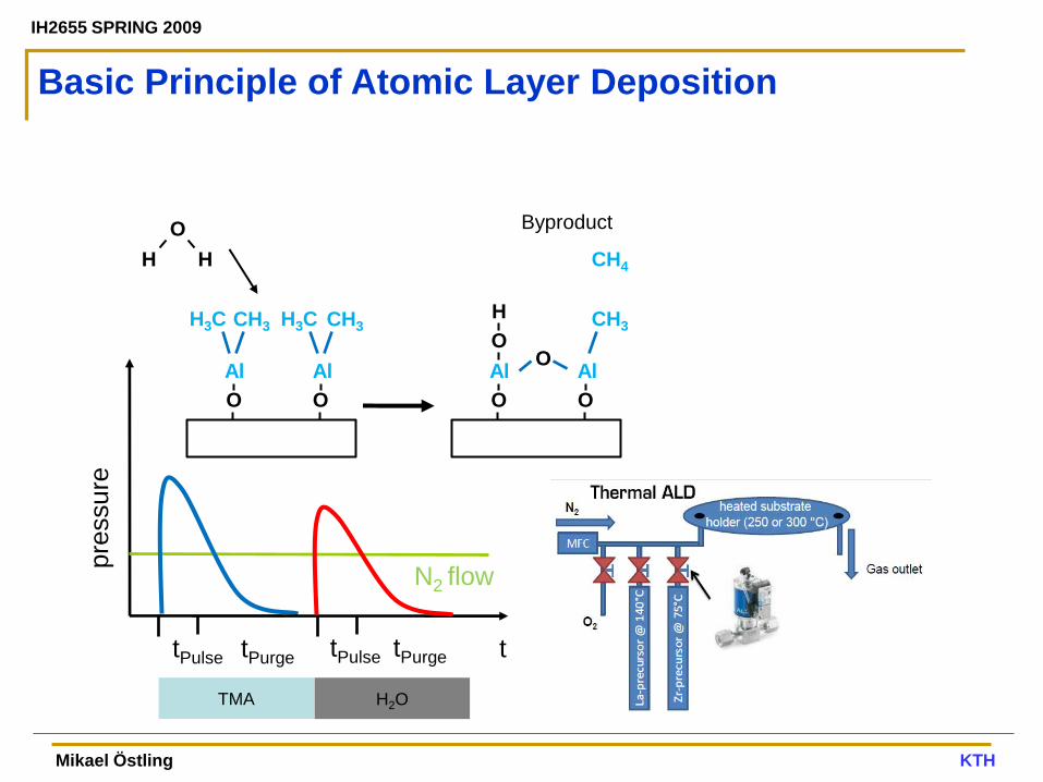
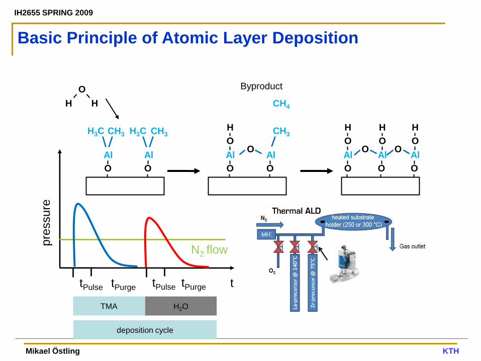
Basic Principle of Atomic Layer Deposition
IH2655 SPRING 2009
Mikael Östling KTH 42
Atomic Layer Deposition (ALD)
• Precise control of depositions down to the atomic scale
• Deposit nanometer thin films with special properties
• Pinhole free coatings, extremely uniform in thickness
• Deposition deep inside pores, trenches, and cavities
• A wide variety of thin films can be deposited (dielectrics and metals)
• A wide range of precursors available (gas, liquid or solid)
• Described in terms of “cycles”, a cycle consists of four basic steps
The principle of ALD is based on sequential pulsing of
chemical precursor vapors, forming one atomic layer
during each pulse sequence.
System in Electrum at KTH used in electronics, MEMS…
IH2655 SPRING 2009
Mikael Östling KTH 43
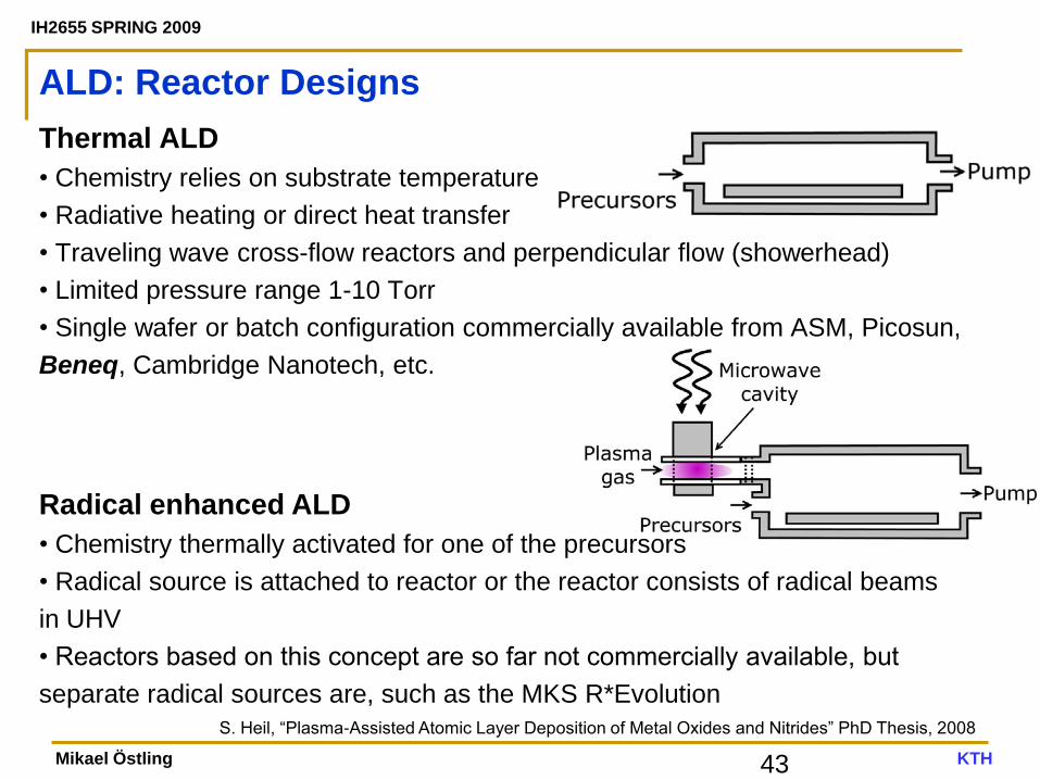
ALD: Reactor Designs
Thermal ALD
• Chemistry relies on substrate temperature
• Radiative heating or direct heat transfer
• Traveling wave cross-flow reactors and perpendicular flow (showerhead)
• Limited pressure range 1-10 Torr
• Single wafer or batch configuration commercially available from ASM, Picosun,
Beneq, Cambridge Nanotech, etc.
Radical enhanced ALD
• Chemistry thermally activated for one of the precursors
• Radical source is attached to reactor or the reactor consists of radical beams
in UHV
• Reactors based on this concept are so far not commercially available, but
separate radical sources are, such as the MKS R*Evolution
S. Heil, “Plasma-Assisted Atomic Layer Deposition of Metal Oxides and Nitrides” PhD Thesis, 2008
IH2655 SPRING 2009
Mikael Östling KTH 44
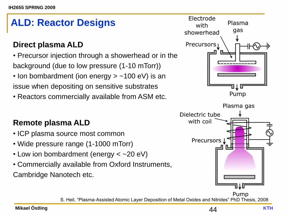
ALD: Reactor Designs
Direct plasma ALD
• Precursor injection through a showerhead or in the
background (due to low pressure (1-10 mTorr))
• Ion bombardment (ion energy > ~100 eV) is an
issue when depositing on sensitive substrates
• Reactors commercially available from ASM etc.
Remote plasma ALD
• ICP plasma source most common
• Wide pressure range (1-1000 mTorr)
• Low ion bombardment (energy < ~20 eV)
• Commercially available from Oxford Instruments,
Cambridge Nanotech etc.
S. Heil, “Plasma-Assisted Atomic Layer Deposition of Metal Oxides and Nitrides” PhD Thesis, 2008
IH2655 SPRING 2009
Mikael Östling KTH
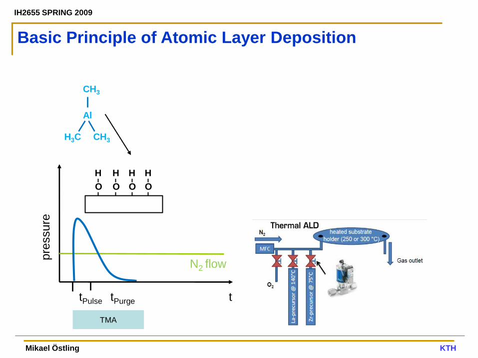
tPulse tPurge
TMA
t
N2 flow
pre
ssure
Basic Principle of Atomic Layer Deposition
O
H
O
H
O
H
O
H
Al
H3C
CH3
CH3
IH2655 SPRING 2009
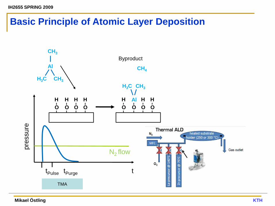
Mikael Östling KTH
tPulse tPurge
TMA
t
pre
ssure
O
H
O
H
O
H
O
H
Al
H3C
CH3
CH3
O
H
O O
H
O
H Al
H3C
CH4
CH3
Byproduct
N2 flow
Basic Principle of Atomic Layer Deposition
IH2655 SPRING 2009
Mikael Östling KTH
tPulse tPurge
TMA
t
pre
ssure
O
H
O
H
O
H
O
H
Al
H3C
CH3
CH3
O
H
O O
H
O
H Al
H3C
CH4
CH3
Byproduct
O O
Al
H3C CH3
Al
H3C CH3
Al
H3C
CH3
CH3
Excess of precursor
N2 flow
Basic Principle of Atomic Layer Deposition
IH2655 SPRING 2009
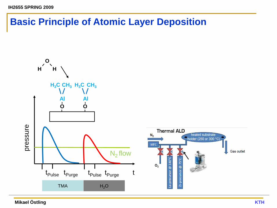
Mikael Östling KTH
O O
Al
H3C CH3
Al
H3C CH3
tPulse tPurge
TMA
t
pre
ssure
H2O
O
H H
tPulse tPurge
N2 flow
Basic Principle of Atomic Layer Deposition
IH2655 SPRING 2009
Mikael Östling KTH
O O
Al
H3C CH3
Al
H3C CH3
tPulse tPurge
TMA
t
pre
ssure
H2O
O
H H
O O
Al Al O
O
H CH3
CH4
Byproduct
tPulse tPurge
N2 flow
Basic Principle of Atomic Layer Deposition
IH2655 SPRING 2009
Mikael Östling KTH
O O
Al
H3C CH3
Al
H3C CH3
tPulse tPurge
TMA
t
pre
ssure
H2O
deposition cycle
O
H H
O O
Al Al O
O
H CH3
CH4
Byproduct
O O
Al Al O
O
H
O
H
O
Al O
O
H
tPulse tPurge
N2 flow
Basic Principle of Atomic Layer Deposition
IH2655 SPRING 2009
Mikael Östling KTH
N2 flow
tPulse tPurge
TMA
t
N2 flow
pre
ssure
H2O
deposition cycle
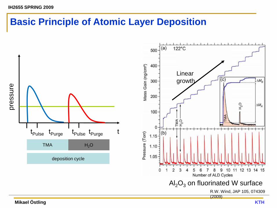
Al2O3 on fluorinated W surface R.W. Wind, JAP 105, 074309
(2009)
Linear
growth
tPulse tPurge
Basic Principle of Atomic Layer Deposition
IH2655 SPRING 2009
Mikael Östling KTH
tPulse tPurge
TMA
t
pre
ssure
H2O
deposition cycle
tPulse tPurge
0
50
100
150
0 500 1000 1500 2000 L
aye
r T
hic
kn
es
s (
nm
) Cycle Number (#)
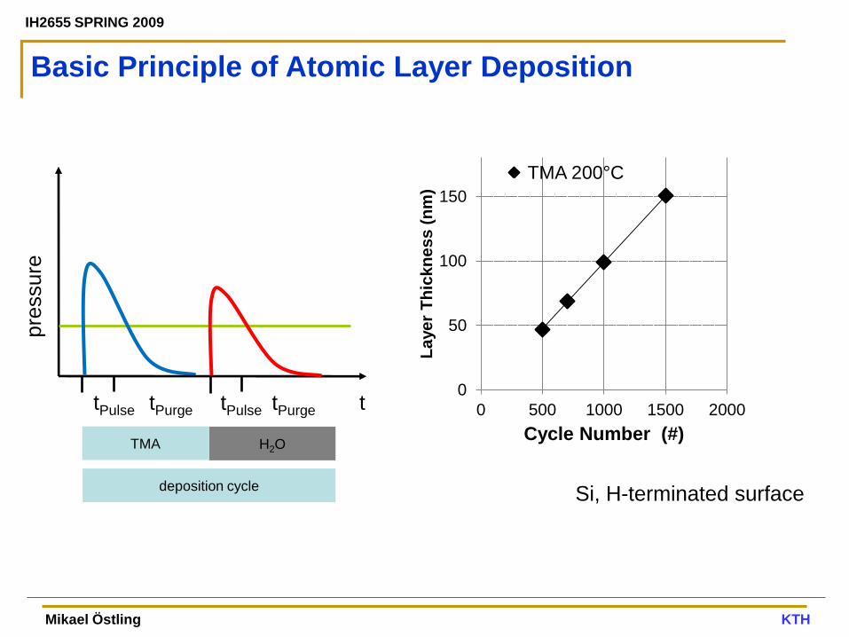
TMA 200°C
Si, H-terminated surface
Basic Principle of Atomic Layer Deposition
IH2655 SPRING 2009
Mikael Östling KTH 53
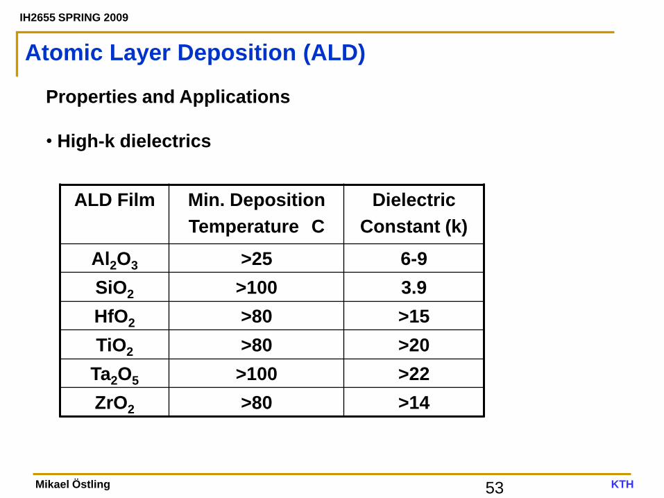
ALD Film Min. Deposition
Temperature C
Dielectric
Constant (k)
Al2O3 >25 6-9
SiO2 >100 3.9
HfO2 >80 >15
TiO2 >80 >20
Ta2O5 >100 >22
ZrO2 >80 >14
Properties and Applications
• High-k dielectrics
Atomic Layer Deposition (ALD)
IH2655 SPRING 2009
Mikael Östling KTH
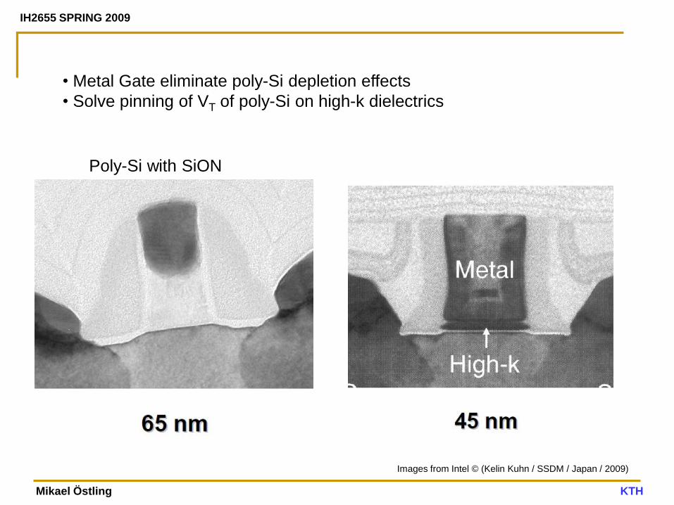
Images from Intel © (Kelin Kuhn / SSDM / Japan / 2009)
• Metal Gate eliminate poly-Si depletion effects
• Solve pinning of VT of poly-Si on high-k dielectrics
Poly-Si with SiON
IH2655 SPRING 2009
Mikael Östling KTH
IH2655 SPRING 2009
Mikael Östling KTH
IH2655 SPRING 2009
Mikael Östling KTH 57
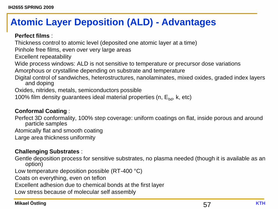
Atomic Layer Deposition (ALD) - Advantages
Perfect films :
Thickness control to atomic level (deposited one atomic layer at a time)
Pinhole free films, even over very large areas
Excellent repeatability
Wide process windows: ALD is not sensitive to temperature or precursor dose variations
Amorphous or crystalline depending on substrate and temperature
Digital control of sandwiches, heterostructures, nanolaminates, mixed oxides, graded index layers and doping
Oxides, nitrides, metals, semiconductors possible
100% film density guarantees ideal material properties (n, Ebd, k, etc)
Conformal Coating :
Perfect 3D conformality, 100% step coverage: uniform coatings on flat, inside porous and around particle samples
Atomically flat and smooth coating
Large area thickness uniformity
Challenging Substrates :
Gentle deposition process for sensitive substrates, no plasma needed (though it is available as an option)
Low temperature deposition possible (RT-400 °C)
Coats on everything, even on teflon
Excellent adhesion due to chemical bonds at the first layer
Low stress because of molecular self assembly