Embed Size (px)
Citation preview

NH – 67, Karur – Trichy Highways, Puliyur C.F, 639 114 Karur District
DEPARTMENT OF ELETRONICS AND COMMUNICATION ENGINEERING
COURSE NOTES
SUBJECT: DIGITAL ELECTRONICS SUBJECT CODE: EC2203
CLASS: II YEAR ECE
UNIT- V
SYNCHRONOUS AND ASYNCHRONOUS SEQUENTIAL CIRCUITS
Synchronous Sequential Circuits: General Model – Classification – Design – Use of
Algorithmic State Machine – Analysis of Synchronous Sequential Circuits
Asynchronous Sequential Circuits: Design of fundamental mode and pulse mode
circuits – Incompletely specified State Machines – Problems in Asynchronous Circuits –
Design of Hazard Free Switching circuits. Design of Combinational and Sequential
circuits using VERILOG
SYNCHRONOUS SEQUENTIAL CIRCUITS
SYNCHRONOUS CIRCUIT
A synchronous circuit is a digital circuit in which the parts are synchronized by a
clock signal.
In an ideal synchronous circuit, every change in the logical levels of its storage
components is simultaneous.
These transitions follow the level change of a special signal called the clock.
Ideally, the input to each storage element has reached its final value before the
next clock occurs, so the behaviour of the whole circuit can be predicted exactly.
Practically, some delay is required for each logical operation, resulting in a
maximum speed at which each synchronous system can run.
ANALYSIS PROCEDURES

This consists of obtaining a table or a diagram for the time sequence of inputs, outputs
and internal states. Boolean expressions can also be written.
STATE EQUATIONS
A state equation specifies the next state as a function of the present state and inputs.
Consider the following sequential circuit:
Since the D input of a flip-flop determines the value of the next state, the equations for
the next state are:
A(t+1) = A(t) x(t) + B(t) x(t)
B(t+1) = A’(t) x(t)

The left-side of each equation denotes the next state of the flip-flop and the right-side
specifies the present state and the conditions that make the next state equal to 1. These
can be expressed in a more compact form by omitting the (t):
A(t+1) = Ax + Bx
B(t+1) = A’x
The present state value of the output can be expressed as:
y(t) =[A(t) + B(t)]x’(t)
The above output equation can be expressed in a more compact form as:
y = (A + B)x’
STATE TABLE
The time sequence of inputs, outputs, and flip-flop states can be enumerated in a state
table. This can be generated from the logic diagram or the state equations. Two
alternative forms for the sequential circuit shown previously are as follows:
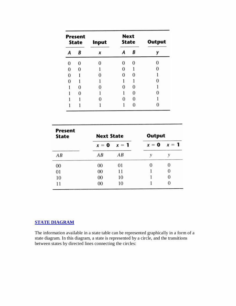
STATE DIAGRAM
The information available in a state table can be represented graphically in a form of a
state diagram. In this diagram, a state is represented by a circle, and the transitions
between states by directed lines connecting the circles:
Each directed lines are labelled with two binary numbers separated by a slash. The input
value during the present state is labelled first, and the number after the slash gives the
output during the present state with the given input. A directed line connecting a circle
with itself indicates that no change of state occurs.
FLIP-FLOP INPUT EQUATIONS
These fully specify the combinational logic that drives the flip-flops and they imply the
type of flipflop from the letter symbol. The input equations for the circuit analysed before
and shown below are:
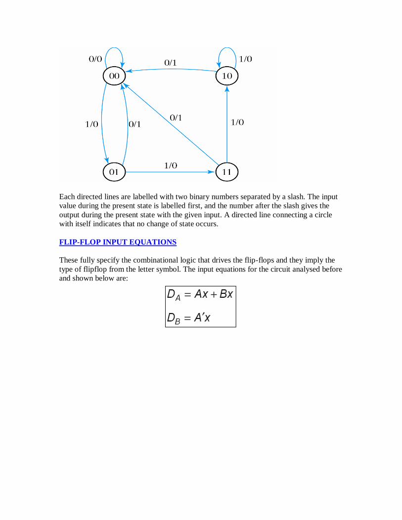
For a D flip-flop, the state equation is the same as the input equation. Input equations are
sometimes called excitation equations.

ANALYSIS WITH D FLIP-FLOPS
Example: Analyze the clocked sequential circuit described by the input equation:
DA = A x y
Solution:
The DA symbol implies a D flip-flop with output A. The x and y variables are the inputs
to the circuit. Since no output equations are given, the output is implied to come from the
output of the flip-flop.The next state values are obtained from the state equation:
A(t+1) = A x y
ANALYSIS WITH JK FLIP-FLOPS
The next state values of a sequential circuit that uses JK or T flip-flops can be derived
from:
A) the characteristic table, or
B) the characteristic equation.
Procedure:
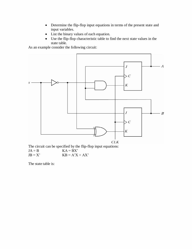
Determine the flip-flop input equations in terms of the present state and
input variables.
List the binary values of each equation.
Use the flip-flop characteristic table to find the next state values in the
state table.
As an example consider the following circuit:
The circuit can be specified by the flip-flop input equations:
JA = B KA = BX’
JB = X’ KB = A’X + AX’
The state table is:

The next state of each flip-flop is determined from the corresponding J and K inputs and
the characteristic table of the JK flip-flop listed below:
ANALYSIS WITH T FLIP-FLOPS
As with JK flip-flops, the next state values can be obtained either by using the
characteristic table:
or by the characteristic equation: Q(t+1) = T Q

Consider the following sequential circuit:
It can be described algebraically by two input equations and an output equation:
TA = BX TB = X y = AB
The state table for this circuit is listed below:

The values for y are obtained from the output equation. The values for the next state can
be derived from the state equations by substituting TA and TB in the characteristic
equations, yielding:
A(t+1) = (BX)’A + (BX)A’ = AB’ + AX’ + A’BX
B(t+1) = X B
The state diagram for the circuit is shown below:
As long as input x is equal to 1, the circuit behaves as a binary counter with a sequence of
states 00, 01, 10, 11, and back to 00.
When x = 0, the circuit remains in the same state. Output y is equal to 1 when the present
state is 11. The output depends on the present state only and is independent of the input.
The two values inside each circle separated by a slash are for the present state and output.
ASYNCHRONOUS SEQUENTIAL CIRCUITS
INTRODUCTION
Do not use clock pulses. The change of internal state occurs when there is a
change in the input variable.
Their memory elements are either unclocked flip-flops or time-delay elements.
They often resemble combinational circuits with feedback.
Their synthesis is much more difficult than the synthesis of clocked synchronous
sequential circuits.
They are used when speed of operation is important.
The communication of two units, with each unit having its own independent clock, must
be done with asynchronous circuits. The general structure of an asynchronous sequential
circuit is as follows:
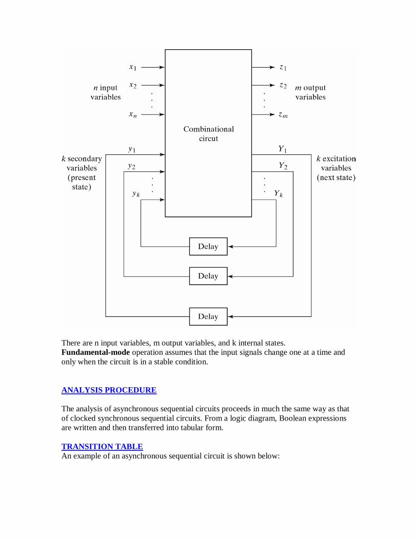
There are n input variables, m output variables, and k internal states.
Fundamental-mode operation assumes that the input signals change one at a time and
only when the circuit is in a stable condition.
ANALYSIS PROCEDURE
The analysis of asynchronous sequential circuits proceeds in much the same way as that
of clocked synchronous sequential circuits. From a logic diagram, Boolean expressions
are written and then transferred into tabular form.
TRANSITION TABLE
An example of an asynchronous sequential circuit is shown below:

The analysis of the circuit starts by considering the excitation variables (Y1 and Y2) as
outputs and the secondary variables (y1 and y2) as inputs.
The next step is to plot the Y1 and Y2 functions in a map:
Combining the binary values in corresponding squares the following transition table is
obtained:

The transition table shows the value of Y = Y1Y2 inside each square. Those entries
where Y = y are circled to indicate a stable condition.
The circuit has four stable total states – y1y2x = 000, 011, 110, and 101 – and four
unstable total states – 001, 010, 111, and 100.
FLOW TABLE
In a flow table the states are named by letter symbols. Examples of flow tables are as
follows:
In order to obtain the circuit described by a flow table, it is necessary to assign to each
state a distinct value. This assignment converts the flow table into a transition table. This
is shown below:

The resulting logic diagram is shown below:
RACE CONDITIONS
A race condition exists in an asynchronous circuit when two or more binary state
variables change value in response to a change in an input variable.
When unequal delays are encountered, a race condition may cause the state
variable to change in an unpredictable manner.
If the final stable state that the circuit reaches does not depend on the order in
which the state variables change, the race is called a non critical race.
Examples of non critical races are illustrated in the transition tables below:
The transition tables below illustrate critical races:

Races can be avoided by directing the circuit through a unique sequence of intermediate
unstable states. When a circuit does that, it is said to have a cycle. Examples of cycles
are:
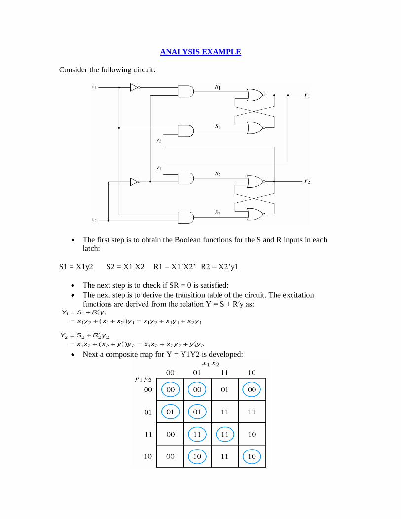
ANALYSIS EXAMPLE
Consider the following circuit:
The first step is to obtain the Boolean functions for the S and R inputs in each
latch:
S1 = X1y2 S2 = X1 X2 R1 = X1’X2’ R2 = X2’y1
The next step is to check if SR = 0 is satisfied:
The next step is to derive the transition table of the circuit. The excitation
functions are derived from the relation Y = S + R′y as:
Next a composite map for Y = Y1Y2 is developed:
Investigation of the transition table reveals that the circuit is stable. There is a critical race
condition when the circuit is initially in total state y1y2x1x2 = 1101 and x2 changes from
1 to 0. If Y1 changes to 0 before Y2, the circuit goes to total state 0100 instead of 0000.
DESIGN PROCEDURE
There are a number of steps that must be carried out in order to minimize the circuit
complexity and to produce a stable circuit without critical races. Briefly, the design steps
are as follows:
1. Obtain a primitive flow table from the given specification.
2. Reduce the flow table by merging rows in the primitive flow table.
3. Assign binary states variables to each row of the reduced flow table to obtain the
transition table.
4. Assign output values to the dashes associated with the unstable states to obtain the
output maps.
5. Simplify the Boolean functions of the excitation and output variables and draw the
logic diagram.
The design process will be demonstrated by going through a specific example:
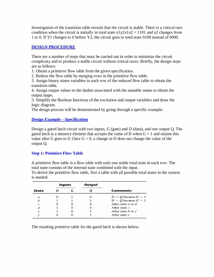
Design Example – Specification
Design a gated latch circuit with two inputs, G (gate) and D (data), and one output Q. The
gated latch is a memory element that accepts the value of D when G = 1 and retains this
value after G goes to 0. Once G = 0, a change in D does not change the value of the
output Q.
Step 1: Primitive Flow Table
A primitive flow table is a flow table with only one stable total state in each row. The
total state consists of the internal state combined with the input.
To derive the primitive flow table, first a table with all possible total states in the system
is needed:
The resulting primitive table for the gated latch is shown below:

First, we fill in one square in each row belonging to the stable state in that row.
Next recalling that both inputs are not allowed to change at the same time, we enter dash
marks in each row that differs in two or more variables from the input variables
associated with the stable state.
Next we find values for two more squares in each row. The comments listed in the
previous table may help in deriving the necessary information. A dash indicates don’t
care conditions.
Step 2: Reduction of the Primitive Flow Table
The primitive flow table can be reduced to a smaller number of rows if two or more
stable states are placed in the same row of the flow table. The simplified merging rules
are as follows:
1. Two or more rows in the primitive flow table can be merged into one if there are
nonconflicting states and outputs in each of the columns.
2. Whenever, one state symbol and don’t care entries are encountered in the same
column, the state is listed in the merged row.
3. If the state is circled in one of the rows, it is also circled in the merged row.
4. The output state is included with each stable state in the merged row.
Now apply these rules to the primitive flow table shown previously.
To see how this is done the primitive flow table is separated into two parts of three rows
each:

Each part shows three stable states that can be merged because there no conflicting
entries in each of the four columns. Since a dash represents a don’t care condition it can
be associated with any state or output. The first column of can be merged into a stable
state c with output 0, the second into a stable state a with output 0, etc.
The resulting reduced flow table is as follows:
Step 3: Transition Table and Logic Diagram
To obtain the circuit described by the reduced flow table, a binary value must be assigned
to each state. This converts the flow table to a transition table.
In assigning binary states, care must be taken to ensure that the circuit will be free of
critical races. No critical races can occur in a two-row flow table.
Assigning 0 to state a and 1 to state b in the reduced flow table, the following transition
table is obtained:
The transition table is, in effect, a map for the excitation variable Y. The simplified
Boolean function for Y as obtained from the map is:
Y = DG +G′’y

There are two don’t care outputs in the final reduced flow table. By assigning values to
the output as shown below:
It is possible to make output Q equal to Y. If the other possible values are assigned to the
don’t care outputs, output Q is made equal to y. In either case, the logic diagram of the
gated latch is as follows:
REDUCTION OF STATE AND FLOW TABLES
The procedure for reducing the number of internal states in an asynchronous sequential
circuit resembles the procedure that is used for synchronous circuits.
IMPLICATION TABLE
The state-reduction procedure for completely specified state tables is based on the
algorithm that two states in a state table can be combined into one if they can be shown to
be equivalent.
There are occasions when a pair of states do not have the same next states, but,
nonetheless, go to equivalent next states. Consider the following state table:

(a, b) imply (c, d) and (c, d) imply (a, b). Both pairs of states are equivalent; i.e., a and b
are equivalent as well as c and d.
The checking of each pair of states for possible equivalence in a table with a large
number of states can be done systematically by means of an implication table. This a
chart that consists of squares, one for every possible pair of states, that provide spaces for
listing any possible implied states. Consider the following state table:
The implication table is:
On the left side along the vertical are listed all the states defined in the state table except
the last, and across the bottom horizontally are listed all the states except the last.
The states that are not equivalent are marked with a ‘x’ in the corresponding square,
whereas their equivalence is recorded with a ‘√’.

Some of the squares have entries of implied states that must be further investigated to
determine whether they are equivalent or not.
The step-by-step procedure of filling in the squares is as follows:
1. Place a cross in any square corresponding to a pair of states whose outputs are not
equal for every input.
2. Enter in the remaining squares the pairs of states that are implied by the pair of states
representing the squares. We do that by starting from the top square in the left column
and going down and then proceeding with the next column to the right.
3. Make successive passes through the table to determine whether any additional squares
should be marked with a ‘x’. A square in the table is crossed out if it contains at least one
implied pair that is not equivalent.
4. Finally, all the squares that have no crosses are recorded with check marks. The
equivalent states are: (a, b), (d, e), (d, g), (e, g).
We now combine pairs of states into larger groups of equivalent states. The last three
pairs can be combined into a set of three equivalent states (d, e, g) because each one of
the states in the group is equivalent to the other two. The final partition of these states
consists of the equivalent states found from the implication table, together with all the
remaining states in the state table that are not equivalent to any other state:
(a, b) (c) (d, e, g) (f)
The reduced state table is:
Merging of the Flow Table
There are occasions when the state table for a sequential circuit is incompletely specified.
Incompletely specified states can be combined to reduce the number of
states in the flow table. Such states cannot be called equivalent, but, instead they are said
to be compatible.
The process that must be applied in order to find a suitable group of compatibles for the
purpose of merging a flow table is divided into three steps:
1. Determine all compatible pairs by using the implication table.
2. Find the maximal compatibles using a merger diagram.
3. Find a minimal collection of compatibles that covers all the states and is closed.
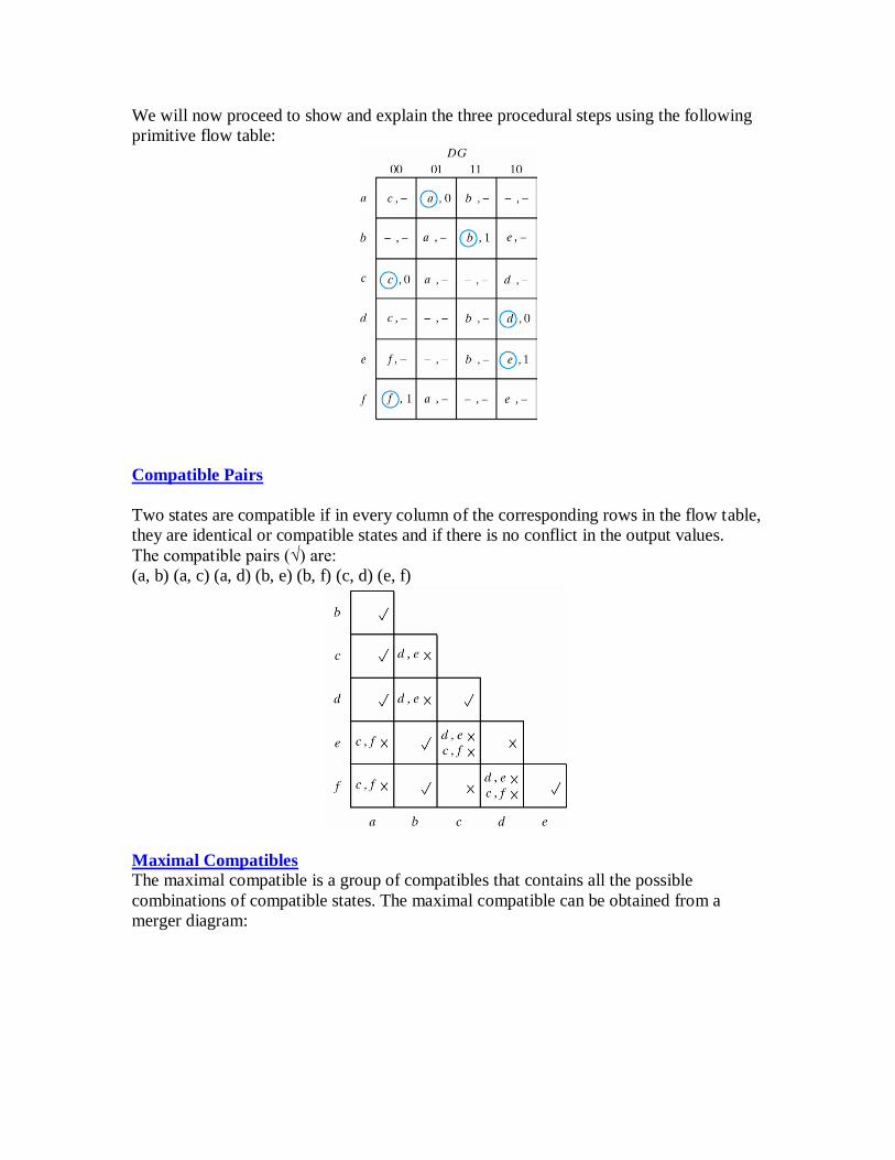
We will now proceed to show and explain the three procedural steps using the following
primitive flow table:
Compatible Pairs
Two states are compatible if in every column of the corresponding rows in the flow table,
they are identical or compatible states and if there is no conflict in the output values.
The compatible pairs (√) are:
(a, b) (a, c) (a, d) (b, e) (b, f) (c, d) (e, f)
Maximal Compatibles
The maximal compatible is a group of compatibles that contains all the possible
combinations of compatible states. The maximal compatible can be obtained from a
merger diagram:

The above merger diagram is obtained from the list of compatible pairs derived from the
previous implication table. A line represents a compatible pair. A triangle constitutes a
compatible with three states. The maximal compatibles are:
(a, b) (a, c, d) (b, e, f)
In the case where a state is not compatible to any other state, an isolated dot represents
this state.
RACE-FREE STATE ASSIGNMENT
The main objective in choosing a proper binary state assignment is the prevention of
critical races.
Critical races are avoided when states between which transitions occur in a flow table are
given adjacent assignments. (e.g., 010 and 111 are adjacent).
No critical races can occur in a two-row flow table.
Three-Row Flow Table Example
Consider the following reduced flow-table. For simplicity the outputs have been omitted:
In row a there is a transition from state a to state c and from state a to state c. This
information is transferred into a transition diagram:
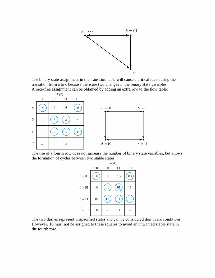
The binary state assignment in the transition table will cause a critical race during the
transition from a to c because there are two changes in the binary state variables.
A race-free assignment can be obtained by adding an extra row to the flow table:
The use of a fourth row does not increase the number of binary state variables, but allows
the formation of cycles between two stable states.
The two dashes represent unspecified states and can be considered don’t care conditions.
However, 10 must not be assigned to these squares to avoid an unwanted stable state in
the fourth row.

Four-Row Flow Table Example
A flow table with four rows requires a minimum of two state variables. Consider the
following flow table and its corresponding transition diagram:
A state assignment map that is suitable for any four-row flow table is shown below:
States a, b, c, and d are the original states, and e, f, and g are extra states. The assignment
ensures that a cycle is produced so that only one binary variable changes at a time.
By using the assignment given by the map, the four-row table can be expanded to a
seven-row table that is free of critical races:
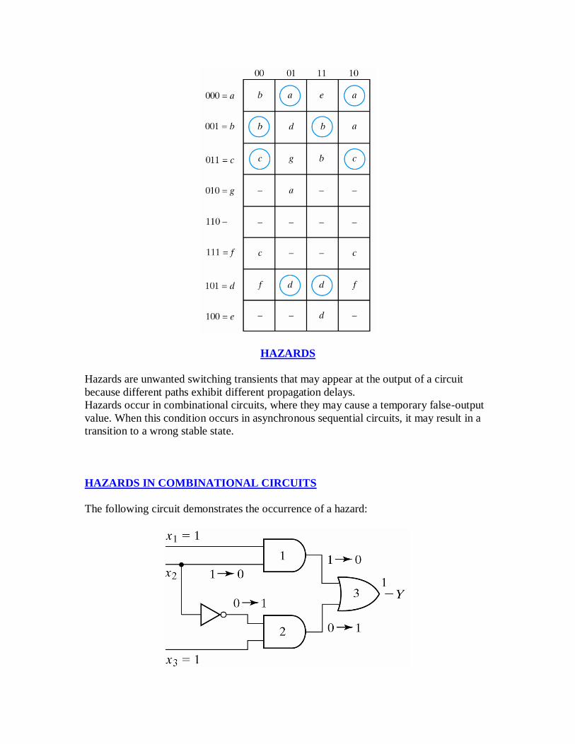
HAZARDS
Hazards are unwanted switching transients that may appear at the output of a circuit
because different paths exhibit different propagation delays.
Hazards occur in combinational circuits, where they may cause a temporary false-output
value. When this condition occurs in asynchronous sequential circuits, it may result in a
transition to a wrong stable state.
HAZARDS IN COMBINATIONAL CIRCUITS
The following circuit demonstrates the occurrence of a hazard:

Assume that all three inputs are initially equal to 1. Then consider a change of x2 from 1
to 0. The output momentarily may go to 0 if the propagation through the inverter is taken
into account.
The circuit implements the Boolean function in sum-of-products
Y = x1x2 + x2’ x3
This type of implementation may cause the output to go to 0 when it should remain a 1.
This is known as a static 1-hazard:
If the circuit was implemented in product-of-sums, namely:
Y = (x1 + x2’ )(x2 + x3 )
Then the output may momentarily go to 1 when it should remain 0. This is referred to as
a static 0-hazard:
A third type of hazard, known as dynamic hazard causes the output to change 2 or 3
time when it should be change from 1 to 0 or 0 to 1:
The occurrence of the hazard can be detected by inspecting the map of the particular
circuit:
Y = x1x2 + x2’x3
The remedy for eliminating a hazard is to enclose the two minterms in question with
another product term that overlaps both groupings:

Y = x1x2 + x2’x3 + x1x3
The hazard-free circuit is:
HAZARDS IN SEQUENTIAL CIRCUITS
Consider the following asynchronous sequential circuit:
If the circuit is in total state yx1x2 = 111 and input x2 changes from 1 to 0, the next total
state should be 110. However, because of the hazard, output Y may go 0 momentarily.
If this false signal feeds back into gate 2 before the output of the inverter goes to 1, the
output of gate 2 will remain at 0 and the circuit will switch to the incorrect total state 010.
This can be eliminated by adding an extra gate.

ESSENTIAL HAZARDS
An essential hazard is the result of the effects of a single input variable change reaching
one feedback path before another feedback path.
Essential hazards cannot be corrected by adding redundant gates as in static hazards.
They can always be eliminated in a realization by the insertion of sufficient delays in the
feedback paths. Facility in doing this comes only with experience.
ASM CHART
Sooner or later you will discover that state diagrams can become very messy. In many
cases just drawing a state diagram includes certain assumptions that are not true in
general. Perhaps certain cases of inputs will never happen, hence the corresponding arcs
are simply not drawn. Certain cases of outputs are not significant and sometimes are left
out. An algorithmic state machine (ASM) diagram offers several advantages over state
diagrams:
For larger state diagrams, often are easier to intpret
conditions for a proper state diagram are automatically satisfied
may be easily coverted to other forms
A key point to remember about ASM charts is that given a state, they do not enumerate
all the possible inputs and outputs. Only the inputs that matter and the outputs that are
asserted are indicated. It must be known whether a signal is positive or negative logic:
Positive logic signals that are high are said to be asserted
Negative logic singals that are low are said to be asserted
In this document, a _n suffix is added to indicate negative logic signals.
THE ASM BLOCK DIAGRAM
An ASM chart has an entry point and is constructed with blocks. A block is constucted
with the following type of symbols.
One state box. The state box has a name and lists
outputs that are asserted when the system is in that
state. These outputs are called synchronous or
Moore type outputs.
Optional decision box(es). A decision box may be
conditioned on a signal or a test of some kind.
Optional conditional output box(es). Such an ouput
box indicates outputs that are conditionally
asserted. These outputs are called asynchrous or
Mealy outputs.

There is no rule saying that outputs are exclusively inside an a conditional output box or
in a state box. An output written inside a state box is simply independent of the input,
while in that state.
The idea is that flow passes from ASM block to ASM block, the decisision boxes decide
the next state and conditional output. Consider the following example of an ASM
diagram block. When state S0 is entered, output Z5 is always asserted. Z1_n however is
asserted only if X2 is also high. Otherwise Z2 is asserted.
An ASM block
CERTAIN RULES
The drawing of ASM charts must follow certain necessary rules:
The entrance paths to an ASM block lead to only one state box Of 'N' possible exit paths,
for each possible valid input combination, only one exit path can be followed, that is
there is only one valid next state.
No feedback internal to a state box is allowed. The following diagram indicates valid and
invalid cases.
Incorrect Correct
PARALLEL VS. SERIAL
We can bend the rules, several internal paths can be active, provided that they lead to a
single exit path. Regardless of parallel or serial form, all tests are performed
concurrently. Usually we have a preference for the serial form. The following two
examples are equivalent.

Parallel Form
Serial Form
SEQUENCE DETECTOR EXAMPLE
The use of ASM charts is a trade-off. While the mechanics of ASM charts do reduce
clutter in significant designs, its better to use an ordinary state diagrams for simple state
machines. Here is an example Moore type state machine with input X and output Z.
Once the flag sequence is received, the output is asserted for one clock cycle.
The corresponding ASM chart is to the right. Note that unlike the state diagram which
illustrates the output value for each arc, the ASM chart indicates when the output Z only
when it is asserted.
State diagram for sequence detector
The following timing diagram illustrates the detection of the desired sequence. Here it is
assumed that the state is updated with a rising clock edge. The key concept to observe is
that regardless of the input, the output can only be asserted for one entire clock cycle.
Timing diagram

EVENT TABLES
Simply stated, timing diagrams are prone to a particular problem for the reader, in that
there can be too much to see. Timing diagrams clearly expresses time relationships and
delay. However, in synchonous sequential logic, all registers are updated at the rising
edge of the system clock. The clock period is just set to an arbitrarily value. Provided
that the input setup-and-hold requirements are satisfied, the details of the timing diagram
are distracting.
The goal of an event table is that given a scenario, to neatly summarize the resultant
behavior of synchronous sequential logic. In writing an event table, capitol T refers to
the system clock period and nT means n times the system clock period. For
asynchronous input changes, the time is given, assuming that the system output reacts
instantaneously. For synchronous signals, the + symbol means a moment suitably after
the given time, for the system to become settled. The - symbol however, means a
moment suitably before the given time, satisfying the necessary setup time.
To reduce the clutter, be sure to fill in those signals that change state or are updated. The
following event table summarizes the behavior in the above timing diagram. An empty
entry will be interpreted to mean no-change to the corresponding signal during the
corresponding clock cycle.
Event Table
Time Reset X State Z
0T 1 0 M0 0
0.4T 0
1T+ M1
1.3T 1
2T+ M2
2.6T 0
3T+ M3 1
3.6T 1
4T+ M2 0
4.4T 0
ASYNCHRONOUS AND SYNCHRONOUS OUTPUT EXAMPLE
The following is an example of an ASM chart with inputs X1 and X2, and outputs Z1 and
Z2. In state S0 the outputs are immediately dependent on the input. In state S1, output
Z1 is always asserted. In state S2, output Z1 is dependent on input X1 but Z2 is not
asserted.

Example ASM chart
The following is the corresponding state diagram. The legend indicates how the input
and output are associated with each arc. The 'd' symbol, which refers here to the don't-
care condition helps to reduce the clutter. While the state diagram and ASM chart here
are similar in complexity, state diagrams quickly become messy.
Corresponding state diagram
CLOCK ENABLE
Simply stated, a clock enable indicates when a state machine must pay attention to the
system clock. The figure below has a clock signal and a clock enable, note that this clock
enable is asserted for one clock period at a time. The clock enable concept is powerful as
it allows a device to effectively be clocked at a rate slower than the system clock, while
remaining entirely synchronous with the rest of the system. In this case the effective
clock rate is one-third that of the system clock.
Clock and enable
In the spirit of reducing clutter, a clock enable can be written next to a state box. When
not asserted, the device remains in its current state. The following figues are equivalent.

Further, it is assumed that devices controlled by such a state, as directly or indirectly
enabled by the clock enable as well.
Equivalent enables
DESIGN OF COMBINATIONAL CIRCUITS USING VERILOG
Eg: Mux : Using assign Statement
//-----------------------------------------------------
// Design Name : mux_using_assign
// File Name : mux_using_assign.v
// Coder : Shabnam
//-----------------------------------------------------
module mux_using_assign(
din_0 , // Mux first input
din_1 , // Mux Second input
sel , // Select input
mux_out // Mux output
);
//-----------Input Ports---------------
input din_0, din_1, sel ;
//-----------Output Ports---------------
output mux_out;
//------------Internal Variables--------
wire mux_out;
//-------------Code Start-----------------
assign mux_out = (sel) ? din_1 : din_0;
endmodule //End Of Module mux

DESIGN OF SEQUENTIAL CIRCUITS USING VERILOG
Eg: 8-Bit Simple Up Counter
//-----------------------------------------------------
// Design Name : up_counter
// File Name : up_counter.v
// Function : Up counter
// Coder : Deepak
//-----------------------------------------------------
module up_counter (
out , // Output of the counter
enable , // enable for counter
clk , // clock Input
reset // reset Input
);
//----------Output Ports--------------
output [7:0] out;
//------------Input Ports--------------
input enable, clk, reset;
//------------Internal Variables--------
reg [7:0] out;
//-------------Code Starts Here-------
always @(posedge clk)
if (reset) begin
out <= 8'b0 ;
end else if (enable) begin
out <= out + 1;
end
endmodule
Summary
Thus this unit provides a brief knowledge about design of synchronous and asynchronous
sequential circuits. It also provides a sound knowledge over design of combinational and
sequential circuits using VERILOG.


![NERCTranslate this page Highlights and Minutes DL/sc...%PDF-1.6 %âãÏÓ 2079 0 obj > endobj 2210 0 obj >/Filter/FlateDecode/ID[6C972F2D19D13C43AD26D8E0E520CE78>1CDB5C06316D994BAD8C608F7002035A>]/Index[2079](https://img.pdfslide.us/doc/110x75/5abe30c77f8b9aa3088c90cc/nerctranslate-this-highlights-and-minutes-dlscpdf-16-2079-0-obj-endobj-2210.jpg)