Embed Size (px)
Citation preview
DEPARTAMENT DE FÍSICA APLICADA i ÒPTICA
Av. Diagonal 647, 08028 Barcelona
THIN FILM NANOCRYSTALLINE SILICON
SOLAR CELLS OBTAINED BY HOT-WIRE CVD
Cristóbal Voz Sánchez
Programa de doctorat: Física i Tecnologia de Materials
Bienni: 1995-1997
Tutor: Manuel Varela Fernández
Director: Jordi Andreu Batallé i José Miguel Asensi López
Memòria presentada per optar al grau de Doctor
Barcelona, Gener 2001

a la família
i els amics
This work has been carried out in the
Department of Applied Physics and Optics of
the University of Barcelona, directed by Dr.
Jordi Andreu and Dr. José Miguel Asensi, in the
framework of the project Crystalline silicon
solar cells on low temperature substrates
(JOR3-CT97-0126) in the JOULE programme
of the European Commission, and also with the
aid of the projects MAT94-262, MAT97-1714-
CE and MAT98-1305-CE of the CICYT of the
Spanish Government.
Thin film nanocrystalline silicon solar cells obtained by Hot-Wire CVD 1
Thin film nanocrystalline silicon solar cells obtained by Hot-Wire CVD Acknowledgments..........................................................................................................
3
Outline of this thesis......................................................................................................
5
1. Introduction................................................................................................................ 7 1.1. The need for renewable energy sources............................................................. 7 1.2. The option for Solar Energy............................................................................... 8 1.3. Thin film technologies for reducing costs.......................................................... 10 1.4. Thin film crystalline silicon solar cells.............................................................. 13 1.5. The brief history of Hot-Wire CVD...................................................................
17
2. The HWCVD set-up. Electrical and optical characterisations................................... 21 2.1. The HWCVD set-up........................................................................................... 21 2.2. Characterisation of samples............................................................................... 26
2.2.1. Dark conductivity..................................................................................... 26 2.2.2. Steady state photoconductivity................................................................ 28 2.2.3. Photothermal deflection spectrometry..................................................... 31
2.3. Characterisation of devices................................................................................ 36 2.3.1. Current density-voltage characteristic..................................................... 36 2.3.2. Spectral response and quantum efficiencies............................................ 38 2.3.3. Depletion capacitance of rectifying contacts...........................................
42
3. Nanocrystalline silicon by HWCVD. Optical and electrical properties.................... 47 3.1. Optical properties............................................................................................... 47
3.1.1. Optical absorption coefficient.................................................................. 47 3.1.2. Enhanced optical absorption.................................................................... 50 3.1.3. Benefits from enhanced optical absorption.............................................. 54 3.1.4. Light scattering........................................................................................ 58 3.1.5. Surface roughness.................................................................................... 59
3.2. Electrical properties........................................................................................... 65 3.2.1. Dark conductivity of undoped nanocrystalline silicon............................ 65 3.2.2. Evidences of contaminants incorporation................................................ 70 3.2.3. Dependence on the deposition rate.......................................................... 72 3.2.4. Effective density of localised states......................................................... 73 3.2.5. Anticorrelation between photoconductivity and layer quality................. 76 3.2.6. Chemical stability....................................................................................
82
4. Physical aspects in thin film p-i-n solar cells............................................................. 85 4.1. Motivation of p-i-n structures............................................................................ 85 4.2. Equivalent circuit of low mobility thin film solar cells..................................... 86
4.2.1. The recombination term........................................................................... 86 4.2.2. Analytical model...................................................................................... 87 4.2.3. The VIM method...................................................................................... 88 4.2.4. The VIM method applied to nc-Si:H p-i-n structures.............................. 92
2 Index
4.3. Collection in p-i-n solar cells............................................................................. 94 4.3.1. The complexity of the problem................................................................ 94 4.3.2. Non uniform internal electric field........................................................... 95 4.3.3. Short circuit recombination losses........................................................... 98 4.3.4. Predictions of the model.......................................................................... 102 4.3.5. The link with the voltage collection........................................................ 104 4.3.6. Contaminated devices..............................................................................
106
5. Nanocrystalline silicon solar cells by HWCVD. Technological aspects................... 111 5.1. Previous technological aspects........................................................................... 111
5.1.1. Selection of the TCO................................................................................ 111 5.1.2. Leakage currents...................................................................................... 116 5.1.3. Doped layers............................................................................................ 118
5.2. The role of the active layer in the device performance...................................... 120 5.2.1. The microdoping approach...................................................................... 120 5.2.2. Influence of the filament temperature...................................................... 125 5.2.3. Cleaner deposition conditions.................................................................. 127 5.2.4. Influence of the substrate temperature..................................................... 130
5.3. Stability of devices.............................................................................................
132
Conclusions....................................................................................................................
135
References......... ............................................................. ..............................................
139
Acronym list............................................................. .....................................................
147
Figure list............................................................. .........................................................
149
Table list............................................................. ...........................................................
155
Resumen en castellano............................................................. .....................................
157
Thin film nanocrystalline silicon solar cells obtained by Hot-Wire CVD 3
Acknowledgements
This Ph. D. Thesis is the result of more than four years of research. Though cooperation
is always necessary to carry out so much work, now I feel that I had not succeeded without
the help of many people:
First of all, I am grateful to Dr. J.L. Morenza, Head of the Department of Applied
Physics and Optics at the University of Barcelona, for accepting me as a Ph. D. student to
participate in this interesting work and for his kindness.
I thoroughly acknowledge Dr. J. Andreu and Dr. J.M. Asensi, codirectors of this thesis,
and also Dr. J. Bertomeu, Dr. J. Puigdollers and Dr. J. Merten, for their wise hints and
sincere friendship.
I am specially grateful to Dr. D. Peiró, who designed the deposition set-up and carried
out all the structural characterisations of the samples. His previous studies have been
essential to the development of this work.
I also acknowledge A. Muñoz, who shared many sometimes boring measurement tasks.
I am also grateful to D. Soler and M. Fonrodona. Though latterly incorporated into the
group, they have greatly cooperated in this thesis with a lot of technological work and
additional points of view.
I am specially grateful to C. Guerrero, F. Benítez and J. Roldán, for their encouraging
support and honest friendship, for the nice time we spent together.
I thank all the other fellows at the laboratory for their help and friendship.
I acknowledge the members of the Thesis Jury, for accepting our invitation and reading
this manuscript.

4 Acknowledgments
Thin film nanocrystalline silicon solar cells obtained by Hot-Wire CVD 5
OUTLINE OF THIS THESIS
The Hot-Wire Chemical Vapor Deposition (HWCVD) allows both low substrate
temperatures and fast deposition rates for obtaining small-grain crystalline silicon films.
These features, along with the low implementation and upkeep costs, make the HWCVD
technique a very attractive technology for a future industrial application. Hence, the
development of this technique was included as one of the main tasks involved in the
project Crystalline silicon solar cells on low temperature substrates CRYSTAL (JOR3-
CT97-0126) in the JOULE programme of the European Commission. This project, led by
BP Solar, was focused on the research of a suitable technology for the mass production of
thin film crystalline silicon solar cells on inexpensive substrates. This thesis started in 1996
and has been developed in the framework of this project. An excellent collateral
work[Peiró, 1999] deals with the design of the new HWCVD set-up in the laboratory and
studies the influence of the deposition parameters on the microstructural properties of the
samples. The present work concerns the optical and electrical properties of these
nanocrystalline silicon layers obtained by HWCVD. Special attention is paid to those
properties which would influence the photovoltaic performance of devices. Besides,
technological and physical aspects about this thin film solar cell technology are considered.
Finally, a comprehensive study of the solar cells obtained by HWCVD during the period of
research within the CRYSTAL project is presented. A brief description of the contents of
each chapter is presented below:
Chapter 1. Introduction
In this chapter we evidence the need for renewable energy sources and we justify our
option for photovoltaics. The thin film option as an alternative for lowering costs is
presented and we review the state of the art in thin film crystalline silicon solar cells.
Finally, we introduce the Hot-Wire Chemical Vapour Deposition as a promising technique
to obtain nanocrystalline silicon inexpensively at high deposition rates.
6 Outline of this thesis
Chapter 2. The HWCVD set-up. Optical and electrical characterisations
This chapter briefly describes the HWCVD set-up at University of Barcelona and the
experimental characterisation techniques used to study the optical and electrical properties
of our layers. An extensive description of the deposition set-up and the structural
characterisation of the samples are part of a previous work[Peiró, 1999]. The specific
characterisations carried out to the obtained devices will also be indicated in this chapter.
Chapter 3. Nanocrystalline silicon by HWCVD. Optical and electrical properties
In this chapter we will study the optical and electrical properties of nanocrystalline silicon
obtained by HWCVD. Special attention will be paid to those properties which clearly
influence the photovoltaic performance of devices. The influence of the deposition
conditions on the photovoltaic suitability of the material is also discussed.
Chapter 4. Physical aspects in thin film p-i-n solar cells
The fundamental understanding of the device performance will be discussed in this
chapter. An extended equivalent circuit and analytical model used in the literature to study
thin film p-i-n structures is briefly described. An improved model which treats analytically
the more general case including a non constant electric field is presented. Chapter 5. Nanocrystalline silicon solar cells by HWCVD. Technological aspects
In this chapter we will consider some subjects which must be taken into account to
fabricate thin film solar cells. Technological aspects such as the selection of a suitable
front electrode or a method to reduce lateral leakage currents are considered. Besides, a
comprehensive study of the p-i-n devices obtained by HWCVD during the period of
research within the CRYSTAL project (JOR3-CT97-0126) is presented.
Thin film nanocrystalline silicon solar cells obtained by Hot-Wire CVD 7
Chapter 1 Introduction
In this chapter we evidence the need for renewable energy sources and we justify our
option for photovoltaics. The thin film option as an alternative for lowering costs is
presented and we review the state of the art in thin film crystalline silicon solar cells.
Finally, we introduce the Hot-Wire Chemical Vapour Deposition as a promising technique
to obtain nanocrystalline silicon inexpensively at high deposition rates.
1.1. The need for renewable energy sources
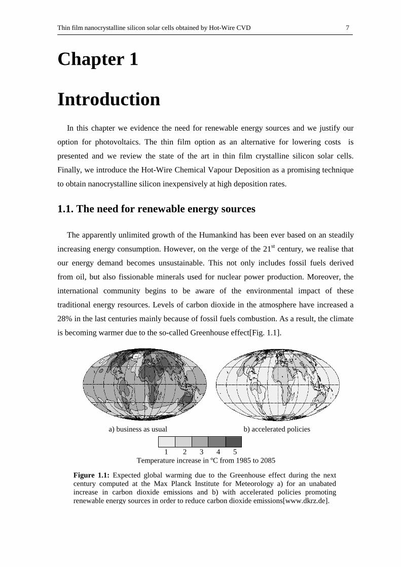
The apparently unlimited growth of the Humankind has been ever based on an steadily
increasing energy consumption. However, on the verge of the 21st century, we realise that
our energy demand becomes unsustainable. This not only includes fossil fuels derived
from oil, but also fissionable minerals used for nuclear power production. Moreover, the
international community begins to be aware of the environmental impact of these
traditional energy resources. Levels of carbon dioxide in the atmosphere have increased a
28% in the last centuries mainly because of fossil fuels combustion. As a result, the climate
is becoming warmer due to the so-called Greenhouse effect[Fig. 1.1].
a) business as usual b) accelerated policies
1 2 3 4 5 Temperature increase in ºC from 1985 to 2085
Figure 1.1: Expected global warming due to the Greenhouse effect during the next century computed at the Max Planck Institute for Meteorology a) for an unabated increase in carbon dioxide emissions and b) with accelerated policies promoting renewable energy sources in order to reduce carbon dioxide emissions[www.dkrz.de].
8 Introduction
This problem could be even exacerbated in the near future by the accompanied
deforestation. On the other hand, the production of nuclear power involves unaffordable
harmful radioactive wastes. By contrast, renewable energy sources will never run out. It is
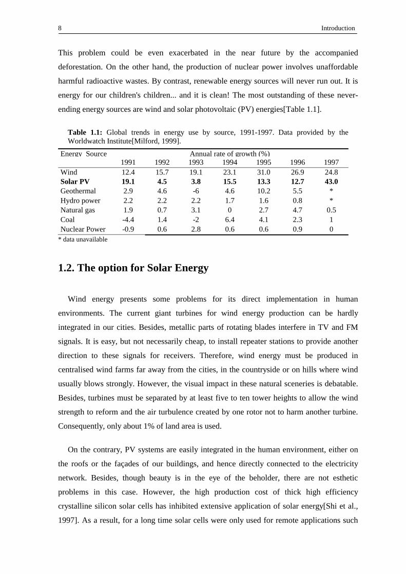
energy for our children's children... and it is clean! The most outstanding of these never-
ending energy sources are wind and solar photovoltaic (PV) energies[Table 1.1].
Table 1.1: Global trends in energy use by source, 1991-1997. Data provided by the Worldwatch Institute[Milford, 1999].
Energy Source Annual rate of growth (%) 1991 1992 1993 1994 1995 1996 1997 Wind 12.4 15.7 19.1 23.1 31.0 26.9 24.8 Solar PV 19.1 4.5 3.8 15.5 13.3 12.7 43.0 Geothermal 2.9 4.6 -6 4.6 10.2 5.5 * Hydro power 2.2 2.2 2.2 1.7 1.6 0.8 * Natural gas 1.9 0.7 3.1 0 2.7 4.7 0.5 Coal -4.4 1.4 -2 6.4 4.1 2.3 1 Nuclear Power -0.9 0.6 2.8 0.6 0.6 0.9 0
* data unavailable
1.2. The option for Solar Energy
Wind energy presents some problems for its direct implementation in human
environments. The current giant turbines for wind energy production can be hardly
integrated in our cities. Besides, metallic parts of rotating blades interfere in TV and FM
signals. It is easy, but not necessarily cheap, to install repeater stations to provide another
direction to these signals for receivers. Therefore, wind energy must be produced in
centralised wind farms far away from the cities, in the countryside or on hills where wind
usually blows strongly. However, the visual impact in these natural sceneries is debatable.
Besides, turbines must be separated by at least five to ten tower heights to allow the wind
strength to reform and the air turbulence created by one rotor not to harm another turbine.
Consequently, only about 1% of land area is used.
On the contrary, PV systems are easily integrated in the human environment, either on
the roofs or the façades of our buildings, and hence directly connected to the electricity
network. Besides, though beauty is in the eye of the beholder, there are not esthetic
problems in this case. However, the high production cost of thick high efficiency
crystalline silicon solar cells has inhibited extensive application of solar energy[Shi et al.,
1997]. As a result, for a long time solar cells were only used for remote applications such
Thin film nanocrystalline silicon solar cells obtained by Hot-Wire CVD 9
as telecommunications and marine navigation systems, where low maintenance and high
reliability are required. Hence, much solar cell research has concentrated on reducing
costs, thus making solar cells commercially viable to generate the energy that we actually
need every day for industry, transportation or space heating.
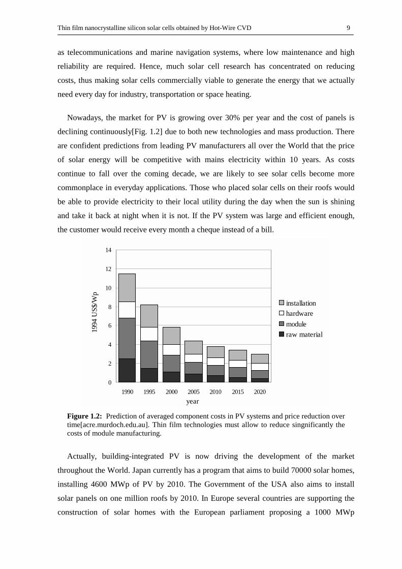
Nowadays, the market for PV is growing over 30% per year and the cost of panels is
declining continuously[Fig. 1.2] due to both new technologies and mass production. There
are confident predictions from leading PV manufacturers all over the World that the price
of solar energy will be competitive with mains electricity within 10 years. As costs
continue to fall over the coming decade, we are likely to see solar cells become more
commonplace in everyday applications. Those who placed solar cells on their roofs would
be able to provide electricity to their local utility during the day when the sun is shining
and take it back at night when it is not. If the PV system was large and efficient enough,
the customer would receive every month a cheque instead of a bill.
0
2
4
6
8
10
12
14
1990 1995 2000 2005 2010 2015 2020
installationhardwaremoduleraw material
year
1994
US$
/Wp
Figure 1.2: Prediction of averaged component costs in PV systems and price reduction over time[acre.murdoch.edu.au]. Thin film technologies must allow to reduce singnificantly the costs of module manufacturing.
Actually, building-integrated PV is now driving the development of the market
throughout the World. Japan currently has a program that aims to build 70000 solar homes,
installing 4600 MWp of PV by 2010. The Government of the USA also aims to install
solar panels on one million roofs by 2010. In Europe several countries are supporting the
construction of solar homes with the European parliament proposing a 1000 MWp
10 Introduction
scheme[Palz, 2000]. In these projects solar cells are incorporated into roofing materials,
cladding and windows. In this way, system costs are reduced by considering the price that
standard building materials would suppose. The Pompeu Fabra public library in the city
center of Mataro (53 kWp) or the PV roof in the City Hall of Barcelona (100 kWp) are our
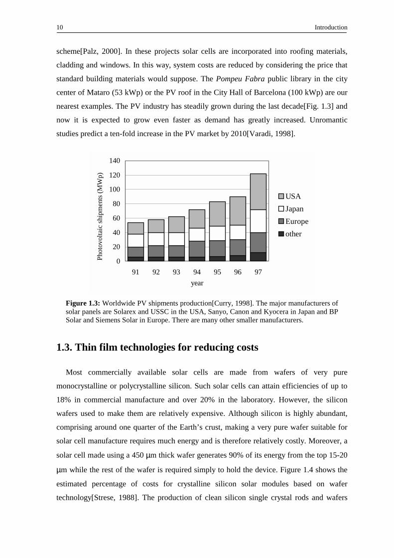
nearest examples. The PV industry has steadily grown during the last decade[Fig. 1.3] and
now it is expected to grow even faster as demand has greatly increased. Unromantic
studies predict a ten-fold increase in the PV market by 2010[Varadi, 1998].
0
20
40
60
80
100
120
140
91 92 93 94 95 96 97
USAJapanEuropeother
year
Phot
ovol
taic
ship
men
ts (M
Wp)
Figure 1.3: Worldwide PV shipments production[Curry, 1998]. The major manufacturers of solar panels are Solarex and USSC in the USA, Sanyo, Canon and Kyocera in Japan and BP Solar and Siemens Solar in Europe. There are many other smaller manufacturers.
1.3. Thin film technologies for reducing costs Most commercially available solar cells are made from wafers of very pure
monocrystalline or polycrystalline silicon. Such solar cells can attain efficiencies of up to
18% in commercial manufacture and over 20% in the laboratory. However, the silicon
wafers used to make them are relatively expensive. Although silicon is highly abundant,
comprising around one quarter of the Earth’s crust, making a very pure wafer suitable for
solar cell manufacture requires much energy and is therefore relatively costly. Moreover, a
solar cell made using a 450 µm thick wafer generates 90% of its energy from the top 15-20
µm while the rest of the wafer is required simply to hold the device. Figure 1.4 shows the
estimated percentage of costs for crystalline silicon solar modules based on wafer
technology[Strese, 1988]. The production of clean silicon single crystal rods and wafers
Thin film nanocrystalline silicon solar cells obtained by Hot-Wire CVD 11
11%
36%
26%
27%
production of pure Si single crystal rodsproduction of Si wafersproduction of cellsproduction of modules
represent the 38% of the total cost, which is certainly a very high percentage for the raw
material only. Besides, in this study pure silicon was assumed to be available as waste
from the semiconductor industry with a very low price[Strese, 1988]. When scaling up the
production, this point could change drastically when such waste feedstock became
insufficient.
Figure 1.4: Percentage of costs for the production of crystalline-Si photovoltaic modules based on wafer technology (450 µm).
Figure 1.5: Typical thin film solar cell structure. Glass is used as a carrier for the front electrode and the active device, in this case a p-i-n structure. Contacts are usually thin metallic films thermally evaporated in high vacuum.
Undoubtedly, one possibility for significantly reducing costs is the development of thin
film solar cell technologies. There are many advantages in thin film solar cells, such as the
ability to be deposited over large areas on inexpensive substrates or building materials, the
ease of mass production and the high suitability to large applications. In the long term, thin
film silicon technology should indeed replace bulk crystalline silicon devices for most
applications which demand inexpensive large area solar panels[Green, 1994]. These
photovoltaic devices usually consists in semiconductor p-i-n structures deposited at
light
contact
contact
TCO glass
n
i
p
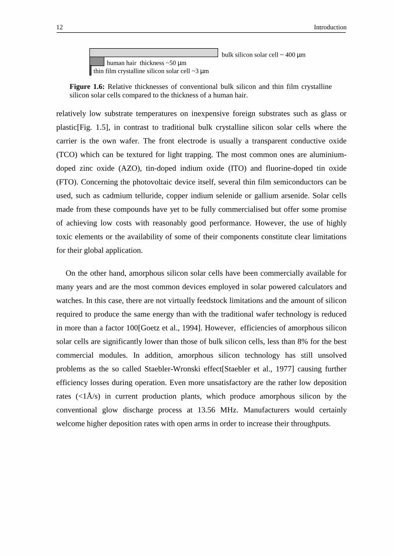
12 Introduction
relatively low substrate temperatures on inexpensive foreign substrates such as glass or
plastic[Fig. 1.5], in contrast to traditional bulk crystalline silicon solar cells where the
carrier is the own wafer. The front electrode is usually a transparent conductive oxide
(TCO) which can be textured for light trapping. The most common ones are aluminium-
doped zinc oxide (AZO), tin-doped indium oxide (ITO) and fluorine-doped tin oxide
(FTO). Concerning the photovoltaic device itself, several thin film semiconductors can be
used, such as cadmium telluride, copper indium selenide or gallium arsenide. Solar cells
made from these compounds have yet to be fully commercialised but offer some promise
of achieving low costs with reasonably good performance. However, the use of highly
toxic elements or the availability of some of their components constitute clear limitations
for their global application.
On the other hand, amorphous silicon solar cells have been commercially available for
many years and are the most common devices employed in solar powered calculators and
watches. In this case, there are not virtually feedstock limitations and the amount of silicon
required to produce the same energy than with the traditional wafer technology is reduced
in more than a factor 100[Goetz et al., 1994]. However, efficiencies of amorphous silicon
solar cells are significantly lower than those of bulk silicon cells, less than 8% for the best
commercial modules. In addition, amorphous silicon technology has still unsolved
problems as the so called Staebler-Wronski effect[Staebler et al., 1977] causing further
efficiency losses during operation. Even more unsatisfactory are the rather low deposition
rates (<1Å/s) in current production plants, which produce amorphous silicon by the
conventional glow discharge process at 13.56 MHz. Manufacturers would certainly
welcome higher deposition rates with open arms in order to increase their throughputs.
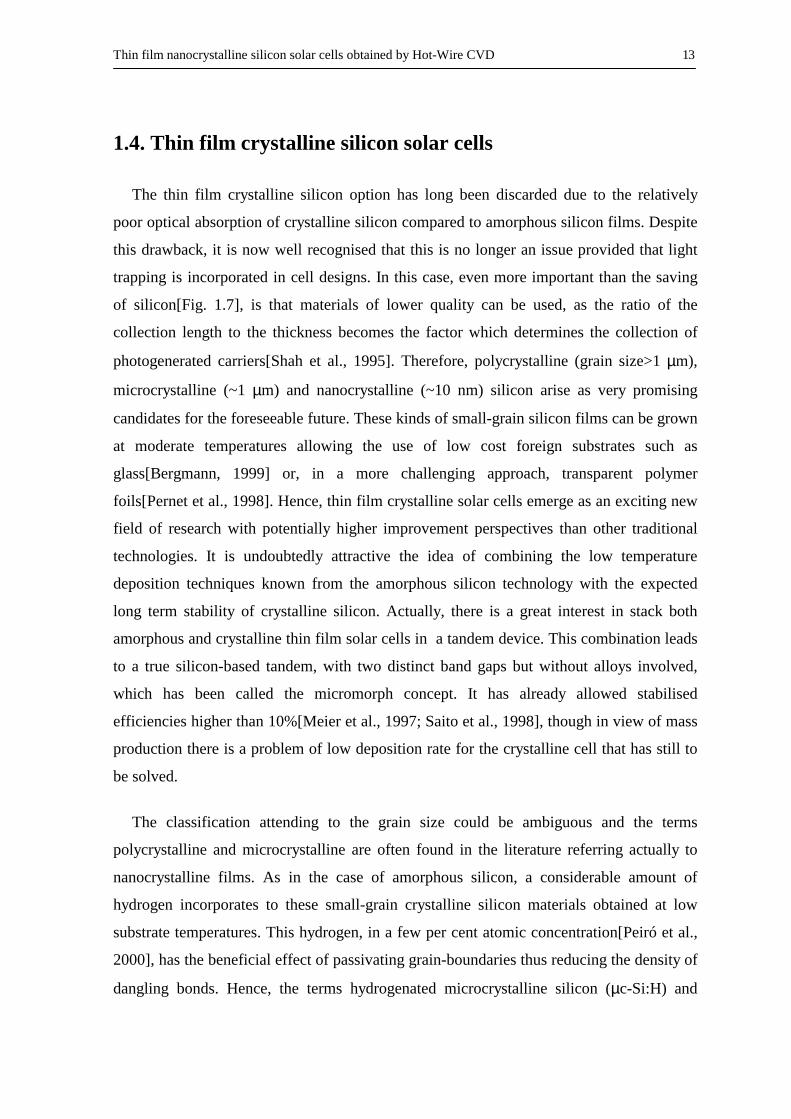
bulk silicon solar cell ~ 400 µm human hair thickness ~50 µm thin film crystalline silicon solar cell ~3 µm
Figure 1.6: Relative thicknesses of conventional bulk silicon and thin film crystalline silicon solar cells compared to the thickness of a human hair.
Thin film nanocrystalline silicon solar cells obtained by Hot-Wire CVD 13
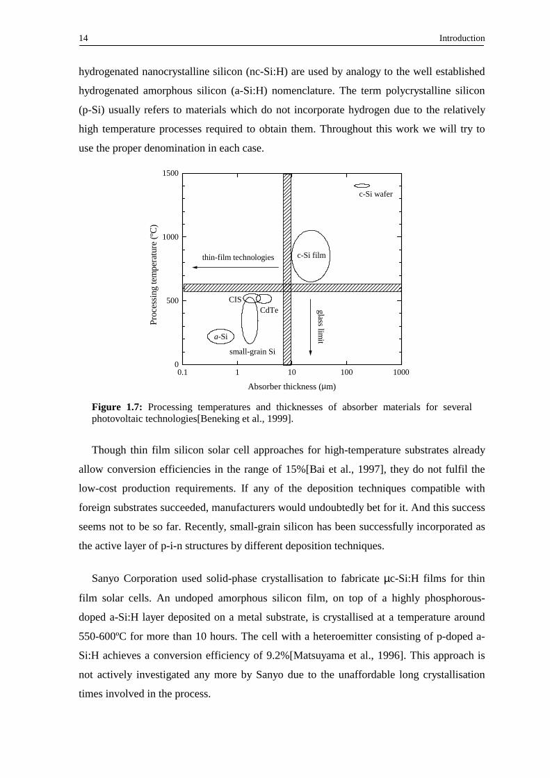
1.4. Thin film crystalline silicon solar cells
The thin film crystalline silicon option has long been discarded due to the relatively
poor optical absorption of crystalline silicon compared to amorphous silicon films. Despite
this drawback, it is now well recognised that this is no longer an issue provided that light
trapping is incorporated in cell designs. In this case, even more important than the saving
of silicon[Fig. 1.7], is that materials of lower quality can be used, as the ratio of the
collection length to the thickness becomes the factor which determines the collection of
photogenerated carriers[Shah et al., 1995]. Therefore, polycrystalline (grain size>1 µm),
microcrystalline (~1 µm) and nanocrystalline (~10 nm) silicon arise as very promising
candidates for the foreseeable future. These kinds of small-grain silicon films can be grown
at moderate temperatures allowing the use of low cost foreign substrates such as
glass[Bergmann, 1999] or, in a more challenging approach, transparent polymer
foils[Pernet et al., 1998]. Hence, thin film crystalline solar cells emerge as an exciting new
field of research with potentially higher improvement perspectives than other traditional
technologies. It is undoubtedly attractive the idea of combining the low temperature
deposition techniques known from the amorphous silicon technology with the expected
long term stability of crystalline silicon. Actually, there is a great interest in stack both
amorphous and crystalline thin film solar cells in a tandem device. This combination leads
to a true silicon-based tandem, with two distinct band gaps but without alloys involved,
which has been called the micromorph concept. It has already allowed stabilised
efficiencies higher than 10%[Meier et al., 1997; Saito et al., 1998], though in view of mass
production there is a problem of low deposition rate for the crystalline cell that has still to
be solved.
The classification attending to the grain size could be ambiguous and the terms
polycrystalline and microcrystalline are often found in the literature referring actually to
nanocrystalline films. As in the case of amorphous silicon, a considerable amount of
hydrogen incorporates to these small-grain crystalline silicon materials obtained at low
substrate temperatures. This hydrogen, in a few per cent atomic concentration[Peiró et al.,
2000], has the beneficial effect of passivating grain-boundaries thus reducing the density of
dangling bonds. Hence, the terms hydrogenated microcrystalline silicon (µc-Si:H) and
14 Introduction
hydrogenated nanocrystalline silicon (nc-Si:H) are used by analogy to the well established
hydrogenated amorphous silicon (a-Si:H) nomenclature. The term polycrystalline silicon
(p-Si) usually refers to materials which do not incorporate hydrogen due to the relatively
high temperature processes required to obtain them. Throughout this work we will try to
use the proper denomination in each case.
0.1 1 10 100 10000
500
1000
1500
thin-film technologies
glass limit
CISCdTe
c-Si wafer
c-Si film
small-grain Si
a-Si
Absorber thickness (µm)
Proc
essin
g te
mpe
ratu
re (º
C)
Figure 1.7: Processing temperatures and thicknesses of absorber materials for several photovoltaic technologies[Beneking et al., 1999].
Though thin film silicon solar cell approaches for high-temperature substrates already
allow conversion efficiencies in the range of 15%[Bai et al., 1997], they do not fulfil the
low-cost production requirements. If any of the deposition techniques compatible with
foreign substrates succeeded, manufacturers would undoubtedly bet for it. And this success
seems not to be so far. Recently, small-grain silicon has been successfully incorporated as
the active layer of p-i-n structures by different deposition techniques.
Sanyo Corporation used solid-phase crystallisation to fabricate µc-Si:H films for thin
film solar cells. An undoped amorphous silicon film, on top of a highly phosphorous-
doped a-Si:H layer deposited on a metal substrate, is crystallised at a temperature around
550-600ºC for more than 10 hours. The cell with a heteroemitter consisting of p-doped a-
Si:H achieves a conversion efficiency of 9.2%[Matsuyama et al., 1996]. This approach is
not actively investigated any more by Sanyo due to the unaffordable long crystallisation
times involved in the process.
Thin film nanocrystalline silicon solar cells obtained by Hot-Wire CVD 15
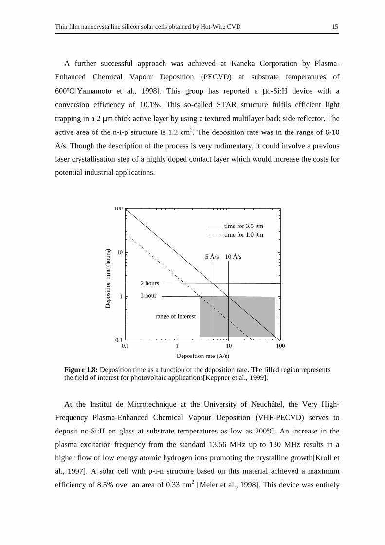
A further successful approach was achieved at Kaneka Corporation by Plasma-
Enhanced Chemical Vapour Deposition (PECVD) at substrate temperatures of
600ºC[Yamamoto et al., 1998]. This group has reported a µc-Si:H device with a
conversion efficiency of 10.1%. This so-called STAR structure fulfils efficient light
trapping in a 2 µm thick active layer by using a textured multilayer back side reflector. The
active area of the n-i-p structure is 1.2 cm2. The deposition rate was in the range of 6-10
Å/s. Though the description of the process is very rudimentary, it could involve a previous
laser crystallisation step of a highly doped contact layer which would increase the costs for
potential industrial applications.
0.1 1 10 1000.1
1
10
100
range of interest
5 Å/s 10 Å/s
2 hours
1 hour
time for 3.5 µmtime for 1.0 µm
Deposition rate (Å/s)
Dep
ositi
on ti
me
(hou
rs)
Figure 1.8: Deposition time as a function of the deposition rate. The filled region represents the field of interest for photovoltaic applications[Keppner et al., 1999].
At the Institut de Microtechnique at the University of Neuchâtel, the Very High-
Frequency Plasma-Enhanced Chemical Vapour Deposition (VHF-PECVD) serves to
deposit nc-Si:H on glass at substrate temperatures as low as 200ºC. An increase in the
plasma excitation frequency from the standard 13.56 MHz up to 130 MHz results in a
higher flow of low energy atomic hydrogen ions promoting the crystalline growth[Kroll et
al., 1997]. A solar cell with p-i-n structure based on this material achieved a maximum
efficiency of 8.5% over an area of 0.33 cm2 [Meier et al., 1998]. This device was entirely
16 Introduction
grown by VHF-PECVD on FTO(Asahi-U ) without any previous solid-phase or laser-
crystallisation step. Neither sophisticated light-trapping strategies were used apart from a
relatively simple back reflector consisting of an AZO/Ag bilayer. The main problem with
this device was the indeed low deposition rate only around 2 Å/s[Fig. 1.8]. Hence, almost 5
hours were required to grow the 3.5 µm thick undoped nc-Si:H active layer. Nevertheless,
the enhancement of the deposition rate up to 10 Å/s (<1 hour) still resulted in a 5.2 %
efficiency solar cell[Torres, 1998]. Though these results are extremely encouraging, set-
ups and components designed to operate at these very high frequencies are at very early
commercialisation stage. This would suppose a drawback for an easy industrialisation of
the VHF-PECVD technique. Similar results were recently obtained by this technique at the
Research Center Jülich in Germany which has reported a 7.5% p-i-n nc-Si:H solar cell with
an active area of 0.7 cm2[Vetterl et al., 1999].
The different approach that we have chosen at University of Barcelona is the Hot-Wire
Chemical Vapour Deposition (HWCVD) technique. To date, HWCVD has allowed the
highest deposition rates of thin film nanocrystalline silicon layers ever reported. Several
tens of Å/s can be easily achieved maintaining reasonably good microstructural
properties[Cifre et al., 1994]. Furthermore, a HWCVD set-up is easier to handle and the
implementation and upkeep costs are much lower than in a PECVD one. Very hopeful
results have been obtained by this technique at the Debye Institute of University of Utrecht
which has reported a 4.4% efficiency nc-Si:H solar cell on stainless steel obtained at a
substrate temperature lower than 500 ºC[Schropp et al., 1999]. The area of the device was
0.16 cm2 and its thickness only 1.2 µm. Both doped layers of the n-i-p structure were
obtained by PECVD in separate chambers whereas the active layer of the device was
grown by HWCVD in less than 40 minutes. Considering that this device is grown on plain
stainless steel and that the n-layer is rather thick to avoid metal diffusion into the active
layer, it does not benefit much from back reflection. Hence, it would compare favourably
with other a priori more efficient devices.
In the framework of the project which has allowed this work (JOR3-CT97-0126), our
research focused on obtaining thin film crystalline silicon solar cells suitable for low cost
applications. Therefore, high temperature processes must be avoided to allow the use of
inexpensive substrates as glass. Besides, high deposition rates should be achieved in order
to increase the productivity. These requirements discard the use of polycrystalline silicon
Thin film nanocrystalline silicon solar cells obtained by Hot-Wire CVD 17
with a large grain size which either requires expensive substrates compatible with high
temperature processes or is very time consuming in crystallisation techniques. Our choice
was HWCVD on account of its suitability to obtain nc-Si:H inexpensively over large areas
at low substrate temperatures with indeed high deposition rates.
1.5. The brief history of Hot-Wire CVD
In 1979, Wiesmann reported that a-Si:H thin films could be formed by cracking
molecules of silane gas with a carbon or tungsten foil heated to 1400-1600ºC[Wiesmann et
al., 1979]. One year later, he patented this method as thermal CVD[Wiesmann, 1980].
However, his attempt was not successful because the electronic quality of their films was
much worse than the obtained by PECVD at that time. Contrary to Wiesmann’s results,
Matsumura at the Japan Advance Institute of Science at Technology (JAIST) succeeded
some years later in obtaining high quality a-Si:H by decomposing a silane-hydrogen gas
mixture with a tungsten wire[Matsumura, 1986]. He called the method Catalytic CVD
(Cat-CVD) and has always sustained the catalytic character of the reactions that take place
on the surface of the hot wire[Matsumura, 1988]. In 1988, Doyle at University of Colorado
also obtained high quality a-Si:H films by the same method which he called Evaporative
Surface Decomposition (ESD). Mahan and coworkers at the National Renewable Energy
Laboratory (NREL) continued Doyle’s work. They extensively studied the properties of a-
Si:H obtained by this technique and contributed to increase the research in this field. They
first called the method Hot-Wire Chemical Vapour Deposition[Mahan et al., 1991] which
seems to be the denomination most commonly found in the literature. Hence, this is the
name that we have used in this work. Matsumura, who had continued developing this
technique in parallel, demonstrated in 1991 the possibility of obtaining nc-Si:H films by
this method at substrate temperatures only around 300ºC[Matsumura, 1991]. Other groups
achieved later similar results[Dusane et al., 1993] until our group at University of
Barcelona reported the first nc-Si:H films obtained by this method in Europe[Cifre et al.,
1994] with deposition rates over 30 Å/s. Besides, our group showed that doped nc-Si:H
films could be easily obtained by adding controlled amounts of doping gases to the base
silage-hydrogen gas mixture[Puigdollers et al., 1995]. By that time, a-Si:H by HWCVD
had already been incorporated in thin film solar cells with promising results[Papadopoulos
et al., 1993; Nelson et al., 1994]. By contrast, nc-Si:H obtained by this technique was not
incorporated as the active layer of thin film solar cells until recently[Rath et al., 1996].
18 Introduction
Research on HWCVD has gone on and a-Si:H solar cells with initial efficiencies of 9.8%
have been obtained by this technique at deposition rates of 16 Å/s[Mahan et al., 1998],
more than one order of magnitude higher than by the conventional PECVD. To our
knowledge, the best nc-Si:H cell ever obtained by HWCVD is the previously depicted
4.4% efficiency n-i-p structure obtained by the group at the Debye Institute[Schropp et al.,
1999]. Very recently, the group at LPICM in the Ecole Polytechnique of Paris has reported
a 3.6% efficiency n-i-p structure on FTO (Asahi-U ) coated glass[Niikura et al., 2000].
However, the thickness and deposition rate of the active layer is not indicated. Similarly to
the group at the Debye Institute, they only grew the active layer by HWCVD while both
doped layers were obtained by PECVD. Furthermore, both groups profiled the active layer
by varying the deposition conditions (hydrogen dilution) during its growth. These results
seem to indicate that the doped/active layer interface plays an important role in the device
performance and amorphous incubation layers there should be avoided. Apart from PV
applications, a-Si:H[Meiling et al., 1997] and nc-Si:H[Rath et al., 1998; Puigdollers et al.,
2000] by HWCVD have also been successfully incorporated as the active channel of thin
film transistors (TFT).
As far as our laboratory is concerned, the development of the HWCVD technique
started in July 1993 with a very elementary set-up. It was only a monochamber made of
glass which shared the pumping system and gas lines of an existing PECVD installation.
The vacuum specifications and the performance of the pumping system were honestly
quite poor. In spite of that, it allowed us to gain invaluable knowledge about the method.
Moreover, preliminary p-i-n structures which obviously showed very low efficiencies
(<1%) could be obtained in this set-up[Peiró et al., 1997]. It was not until January 1998
that the currently operative new ultra-high vacuum multichamber set-up was available.
This system, extensively described in a previous work[Peiró, 1999], was built at University
of Barcelona during the first two years of research within the CRYSTAL project (JOR3-
CT97-0126) in the JOULE programme of the European Commission. The first device was
obtained in May 1998 after a lot of work to optimise not only the deposition conditions but
also the HWCVD set-up itself. To date, our best solar cell showed a 2.5% conversion
efficiency. It was a p-i-n structure entirely obtained by HWCVD on AZO-coated glass at
an indeed low substrate temperature of 150ºC. The undoped active layer 2.4 µm thick was
obtained at a high deposition rate of 15 Å/s, thus the process time was less than 30
minutes. Neither textured TCO nor back reflector were used and the p-layer was certainly
Thin film nanocrystalline silicon solar cells obtained by Hot-Wire CVD 19
too thick (~500 Å). Hence, just optical losses severely limited the maximum expected
efficiency. Moreover, an n-i-p inverted structure illuminated from the top side would
undoubtedly benefit from the enhanced quality of the material with respect to the initial
stages of growth. This is the case for the 4.4% efficiency device obtained at the Debye
Institute[Schropp et al., 1999]. However, we could not test this structure because the
required low temperature top TCO has still to be optimised. We must say that even now we
are at a early stage of our research and we honestly think that our results are very
encouraging.

20 Introduction
Thin film nanocrystalline silicon solar cells obtained by Hot-Wire CVD 21
Chapter 2 The HWCVD set-up. Electrical and optical characterisations
This chapter briefly describes the HWCVD set-up at University of Barcelona and the
experimental characterisation techniques used to study the optical and electrical properties
of our layers. An extensive description of the deposition set-up and the structural
characterisation of the samples are part of a previous work[Peiró, 1999]. The specific
characterisations carried out to the obtained devices will also be indicated in this chapter.
2.1. The HWCVD set-up
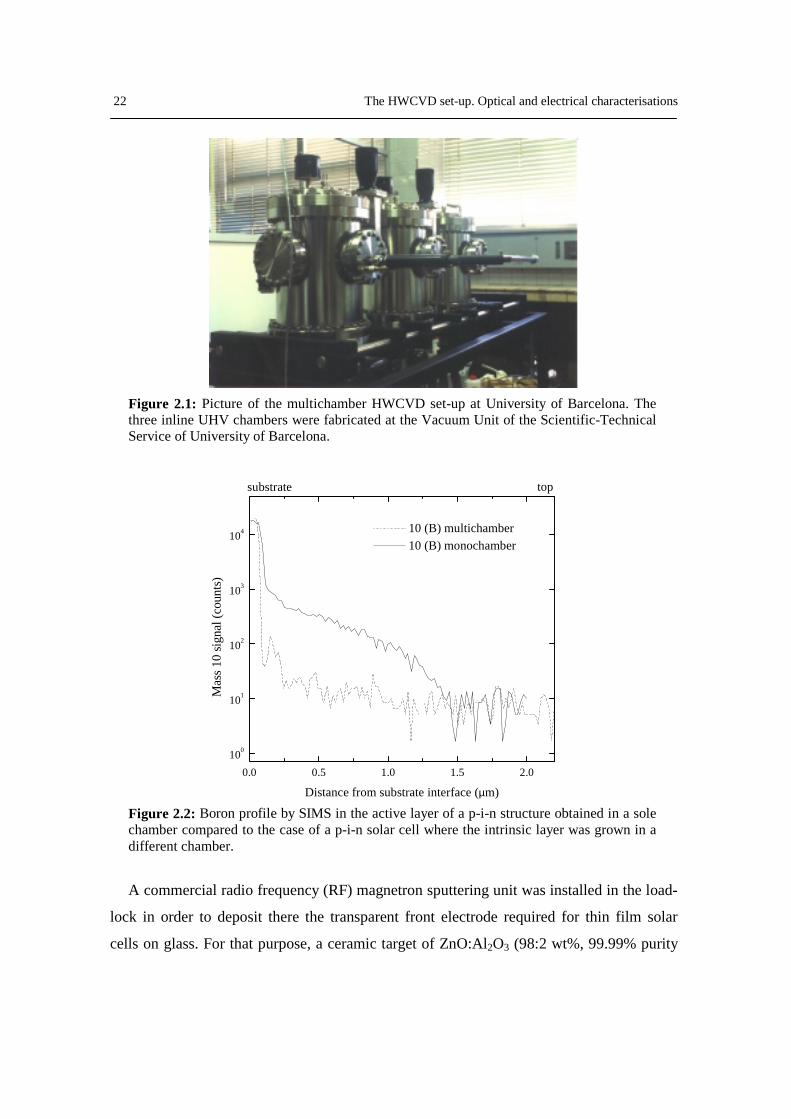
A new HWCVD set-up[Fig. 2.1] was built at University of Barcelona during the first
two years of research within the CRYSTAL project (JOR3-CT97-0126) in the JOULE
programme of the European Commission. This set-up consists of three different ultra-high
vacuum (UHV) chambers isolated between them by gate valves. Only two of the
deposition chambers are intended for HWCVD processes whereas the other one is a load-
lock. A magnetic transfer system is used to locate the substrate in the desired chamber.
Separate chambers are used to grow the doped and intrinsic nc-Si:H layers of devices in
order to avoid undesired cross contamination in the active layer[Voz et al., 2000].
Processes involving doping gases are performed in the HWCVD chamber-2 whereas
chamber-1 is preserved to obtain the undoped active layers of p-i-n solar cells. Figure 2.2
compares the boron profile by Secondary Ion Mass Spectroscopy (SIMS) in the intrinsic
layer of a monochamber p-i-n solar cell to the case of a p-i-n structure whose active layer
was grown in a different chamber. Such contaminated active layer turned out to be
unsuitable for photovoltaic devices due to the screening of the internal electric field within
the active layer. Hence, the multichamber requirement results justified.
22 The HWCVD set-up. Optical and electrical characterisations
Figure 2.1: Picture of the multichamber HWCVD set-up at University of Barcelona. The three inline UHV chambers were fabricated at the Vacuum Unit of the Scientific-Technical Service of University of Barcelona.
0.0 0.5 1.0 1.5 2.0100
101
102
103
104 10 (B) multichamber 10 (B) monochamber
topsubstrate
Distance from substrate interface (µm)
Mas
s 10
signa
l (co
unts)
Figure 2.2: Boron profile by SIMS in the active layer of a p-i-n structure obtained in a sole chamber compared to the case of a p-i-n solar cell where the intrinsic layer was grown in a different chamber.
A commercial radio frequency (RF) magnetron sputtering unit was installed in the load-
lock in order to deposit there the transparent front electrode required for thin film solar
cells on glass. For that purpose, a ceramic target of ZnO:Al2O3 (98:2 wt%, 99.99% purity
Thin film nanocrystalline silicon solar cells obtained by Hot-Wire CVD 23
and 2’’ diameter) was mounted in the sputtering unit to grow aluminium-doped zinc oxide
layers. Therefore, a whole TCO/p-i-n structure can be grown on glass without exposing
any interface to the atmosphere.
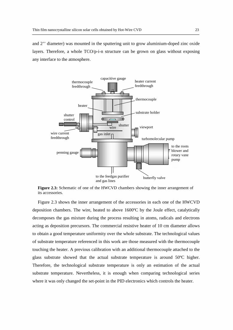
Figure 2.3: Schematic of one of the HWCVD chambers showing the inner arrangement of its accessories.
Figure 2.3 shows the inner arrangement of the accessories in each one of the HWCVD
deposition chambers. The wire, heated to above 1600ºC by the Joule effect, catalytically
decomposes the gas mixture during the process resulting in atoms, radicals and electrons
acting as deposition precursors. The commercial resistive heater of 10 cm diameter allows
to obtain a good temperature uniformity over the whole substrate. The technological values
of substrate temperature referenced in this work are those measured with the thermocouple
touching the heater. A previous calibration with an additional thermocouple attached to the
glass substrate showed that the actual substrate temperature is around 50ºC higher.
Therefore, the technological substrate temperature is only an estimation of the actual
substrate temperature. Nevertheless, it is enough when comparing technological series
where it was only changed the set-point in the PID electronics which controls the heater.
capacitive gauge heater current feedthrough
thermocouple feedthrough
thermocouple substrate holder
heater
wire
gas inlet
shutter control
wire current feedthrough
penning gauge to the roots blower and rotary vane pump
butterfly valve
turbomolecular pump
shutter viewport
to the feedgas purifier and gas lines
24 The HWCVD set-up. Optical and electrical characterisations
pneumaticvalve
manualvalve
manual valve
manualvalve
manualvalve
manual valve
pirani
pirani
pirani
penningcompactpirani-penning
capacitivecapacitive
gas inlets(from gas panels)
common line(from gas panels)
butterflyvalve
turbomolecularpump
rotary vane pump
roots blower
rotary vane pump
exhaust
exhaust
turbomolecularpump
butterflyvalve
manual valve
penning
capacitive
butterflyvalve
turbomolecularpump
HWCVDchamber 2
load-lockand
magnetronsputtering unit
HWCVDchamber 1transfer
system
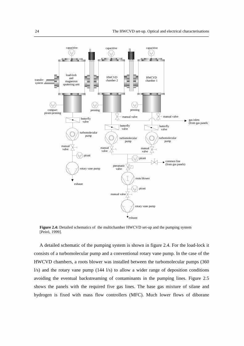
Figure 2.4: Detailed schematics of the multichamber HWCVD set-up and the pumping system [Peiró, 1999].
A detailed schematic of the pumping system is shown in figure 2.4. For the load-lock it
consists of a turbomolecular pump and a conventional rotary vane pump. In the case of the
HWCVD chambers, a roots blower was installed between the turbomolecular pumps (360
l/s) and the rotary vane pump (144 l/s) to allow a wider range of deposition conditions
avoiding the eventual backstreaming of contaminants in the pumping lines. Figure 2.5
shows the panels with the required five gas lines. The base gas mixture of silane and
hydrogen is fixed with mass flow controllers (MFC). Much lower flows of diborane
Thin film nanocrystalline silicon solar cells obtained by Hot-Wire CVD 25
(diluted at 1% into hydrogen) and phosphine (diluted at 5% into silane) are added to obtain
doped layers. Ultrapure gas bottles are used with the following specifications: 4.7
(99.997%) for silane and 6.0 (99.9999%) for hydrogen. Nitrogen is the purging gas. Note
the zeolite feedgas purifier (SAES Getters MonoTorr ) to reduce contaminants (oxygen,
carbon...) in the feedgas lines under ppb levels.
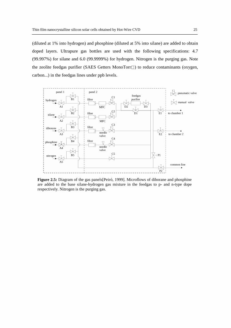
silane
phosphine
hydrogen
diborane
nitrogen
feedgaspurifier
MFC
MFC
common line
to chamber 2
to chamber 1
pneumatic valve
manual valve
panel 1 panel 2
filter
needlevalve
A1
C1
C2
C4E2
P2
P1
E1
C5
C3
B1
B2 D1
D3D2
B3
B4
B5
A2
A4
A3
A5
needlevalve
filter
filter
filter
Figure 2.5: Diagram of the gas panels[Peiró, 1999]. Microflows of diborane and phosphine are added to the base silane-hydrogen gas mixture in the feedgas to p- and n-type dope respectively. Nitrogen is the purging gas.
26 The HWCVD set-up. Optical and electrical characterisations
2.2. Characterisation of samples
In the following sections we describe the different electrical and optical
characterisations performed to the obtained nc-Si:H samples. Here we just briefly describe
the experimental set-ups while specific details on the interpretation of these measurements
are included in the next chapter.
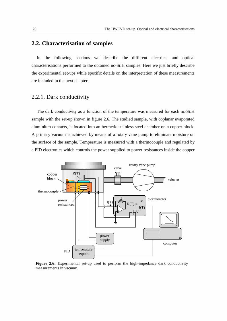
2.2.1. Dark conductivity
The dark conductivity as a function of the temperature was measured for each nc-Si:H
sample with the set-up shown in figure 2.6. The studied sample, with coplanar evaporated
aluminium contacts, is located into an hermetic stainless steel chamber on a copper block.
A primary vacuum is achieved by means of a rotary vane pump to eliminate moisture on
the surface of the sample. Temperature is measured with a thermocouple and regulated by
a PID electronics which controls the power supplied to power resistances inside the copper
power supply
power resistances
copper block exhaust
rotary vane pump
thermocouple
valve
ℜ
V
I(T) electrometer
computer
I(T)
VR(T) =
R(T)
temperature setpoint
PID
Figure 2.6: Experimental set-up used to perform the high-impedance dark conductivity measurements in vacuum.
Thin film nanocrystalline silicon solar cells obtained by Hot-Wire CVD 27
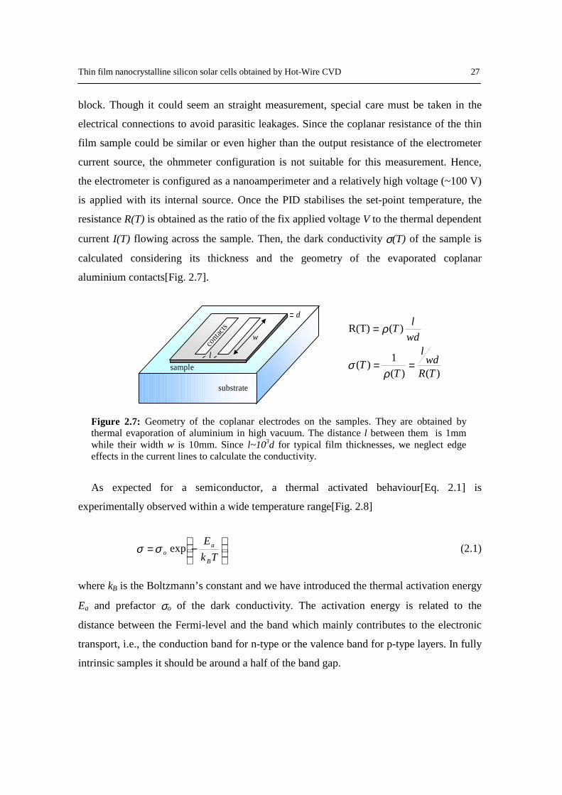
block. Though it could seem an straight measurement, special care must be taken in the
electrical connections to avoid parasitic leakages. Since the coplanar resistance of the thin
film sample could be similar or even higher than the output resistance of the electrometer
current source, the ohmmeter configuration is not suitable for this measurement. Hence,
the electrometer is configured as a nanoamperimeter and a relatively high voltage (~100 V)
is applied with its internal source. Once the PID stabilises the set-point temperature, the
resistance R(T) is obtained as the ratio of the fix applied voltage V to the thermal dependent
current I(T) flowing across the sample. Then, the dark conductivity σ(T) of the sample is
calculated considering its thickness and the geometry of the evaporated coplanar
aluminium contacts[Fig. 2.7].
Figure 2.7: Geometry of the coplanar electrodes on the samples. They are obtained by thermal evaporation of aluminium in high vacuum. The distance l between them is 1mm while their width w is 10mm. Since l~103d for typical film thicknesses, we neglect edge effects in the current lines to calculate the conductivity.
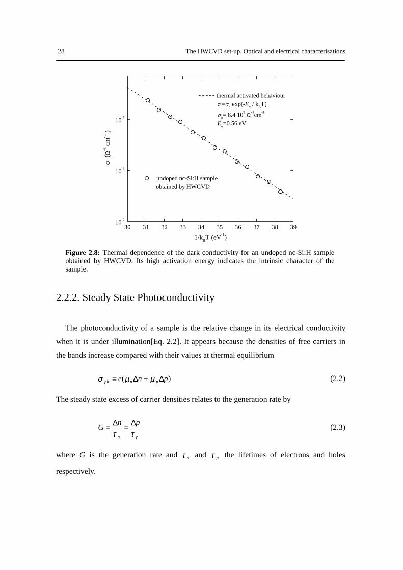
As expected for a semiconductor, a thermal activated behaviour[Eq. 2.1] is
experimentally observed within a wide temperature range[Fig. 2.8]
−=
TkE
B
ao expσσ (2.1)
where kB is the Boltzmann’s constant and we have introduced the thermal activation energy
Ea and prefactor σo of the dark conductivity. The activation energy is related to the
distance between the Fermi-level and the band which mainly contributes to the electronic
transport, i.e., the conduction band for n-type or the valence band for p-type layers. In fully
intrinsic samples it should be around a half of the band gap.
)()(1)(
)(R(T)
TRwd
l
TT
wdlT
==
=
ρσ
ρ
l
w
d
substrate
sample
conta
cts
28 The HWCVD set-up. Optical and electrical characterisations
30 31 32 33 34 35 36 37 38 3910-7
10-6
10-5
thermal activated behaviour σ =σo exp(-Ea / kBT)
σo= 8.4 103 Ω -1cm-1
Ea=0.56 eV
undoped nc-Si:H sample obtained by HWCVD
1/kBT (eV-1)
σ ( Ω
-1 c
m-1 )
Figure 2.8: Thermal dependence of the dark conductivity for an undoped nc-Si:H sample obtained by HWCVD. Its high activation energy indicates the intrinsic character of the sample.
2.2.2. Steady State Photoconductivity
The photoconductivity of a sample is the relative change in its electrical conductivity
when it is under illumination[Eq. 2.2]. It appears because the densities of free carriers in
the bands increase compared with their values at thermal equilibrium
)( pne pnph ∆+∆= µµσ (2.2)
The steady state excess of carrier densities relates to the generation rate by
pn
pnGττ∆=∆= (2.3)
where G is the generation rate and nτ and pτ the lifetimes of electrons and holes
respectively.
Thin film nanocrystalline silicon solar cells obtained by Hot-Wire CVD 29
Therefore, by introducing equation 2.3 in 2.2 we define the steady state
photoconductivity µτ-product as
ppnnph
ph eGτµτµ
σµτ +== (2.4)
Though the µτ-products of both carriers seem to contribute to µτ ph , it is actually
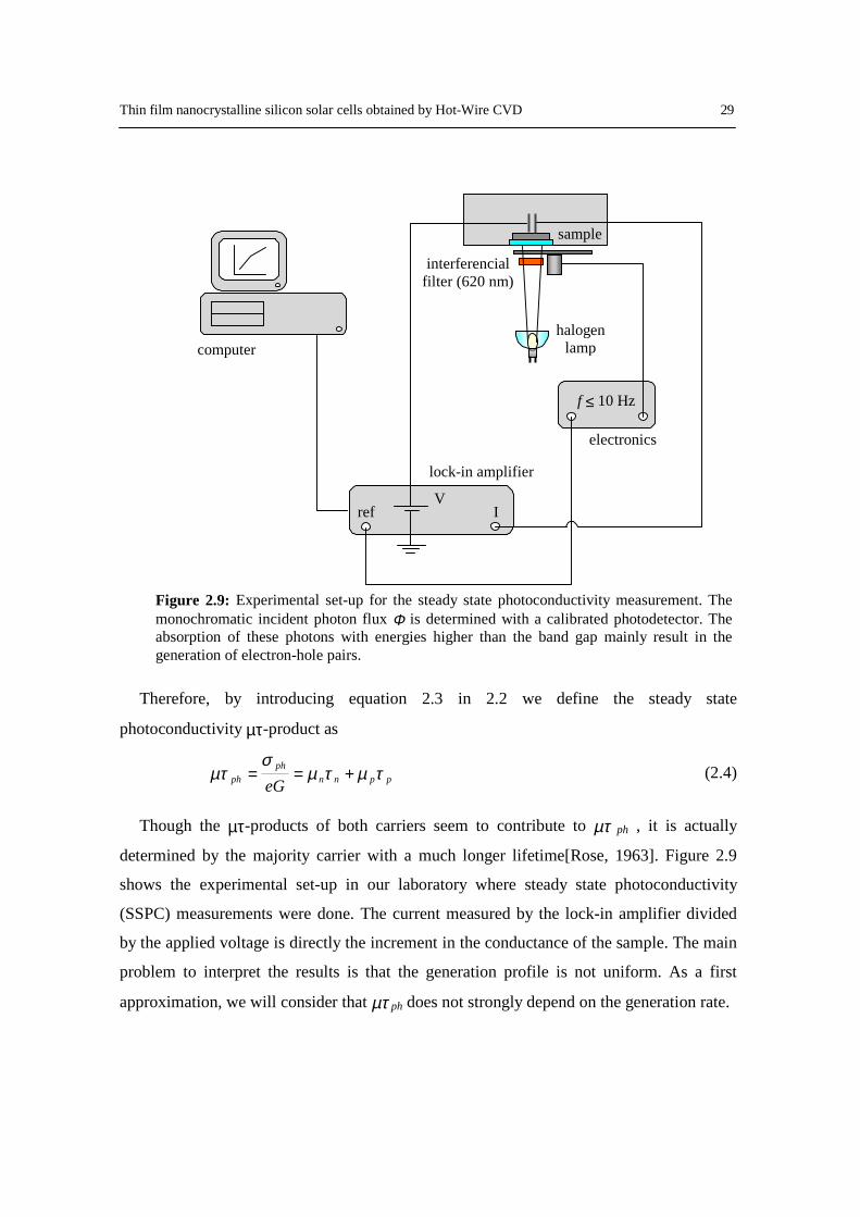
determined by the majority carrier with a much longer lifetime[Rose, 1963]. Figure 2.9
shows the experimental set-up in our laboratory where steady state photoconductivity
(SSPC) measurements were done. The current measured by the lock-in amplifier divided
by the applied voltage is directly the increment in the conductance of the sample. The main
problem to interpret the results is that the generation profile is not uniform. As a first
approximation, we will consider that µτ ph does not strongly depend on the generation rate.
sample
halogen lamp
f ≤ 10 Hz
electronics
computer
lock-in amplifier
I ref V
interferencial filter (620 nm)
Figure 2.9: Experimental set-up for the steady state photoconductivity measurement. The monochromatic incident photon flux Φ is determined with a calibrated photodetector. The absorption of these photons with energies higher than the band gap mainly result in the generation of electron-hole pairs.
30 The HWCVD set-up. Optical and electrical characterisations
Then, if the sample is divided into infinitesimal slides dz and for the same geometry
shown in figure 2.7, we obtain
[ ]lwdedz
lwze
dzlwzGedz
lwz
VI
d
o phph
d
ph
d
ph
∫
∫∫−−=−=
===
)exp(1)exp(
)()(00
αΦµτααΦµτ
µτσ (2.5)
where α is the optical absorption coefficient at the given wavelength. If we define the
mean generation rate according to
[ ]
ddG )exp(1 αΦ −−>=< (2.6)
and the mean photoconductivity as
lwd
VI
ph >=<σ (2.7)
from equations 2.5-2.7 we arrive at
><>=< Ge phph µτσ (2.8)
In practice, it is observed a power-law behaviour <σ ph>~<G>γ in most nc-Si:H samples
with γ<1 [Goerlitzer et al., 1996] because µτ ph actually depends on the generation
rate[Fig. 2.10]. Thus, reported SSPC µτ-products of different samples can not be compared
as long as the experimental conditions for the measurement are not indicated. Furthermore,
active layers with higher values of µτ ph do not necessary imply an enhanced photovoltaic
performance but an undesired Fermi-level shift due to the incorporation
contaminants[Section 3.2.5]. Nevertheless, it is a useful an easy technique to compare
samples measured under similar generation profiles.
Thin film nanocrystalline silicon solar cells obtained by Hot-Wire CVD 31
1017 1018 1019
10-8
10-7
10-6
mean photoconductivity
<σ ph > ~ <G>γ with γ =1-λ= 0.85
µτ ph (cm
2 /V)
<G> (cm-3 s-1 )
< σ ph
> (
Ω-1
cm-1
)
10-7
10-6
10-5
photoconductivity µτ -product
µτ ph ~ <G>−λ with λ=0.15
Figure 2.10: Mean steady state photoconductivity and SSPC µτ-product as a function of the mean generation rate for a typical undoped nc-Si:H sample obtained by HWCVD. A sublinear behaviour <σ ph>~<G>γ with γ =0.85 is observed because µτ ph significantly depends on the generation rate.
2.2.3. Photothermal Deflection Spectrometry
The Photothermal Deflection Spectrometry (PDS) technique allows confident
measurements of very low optical absorptions in the range of αd<10-5. For comparison,
conventional absorption measurements with combined transmittance-reflectance spectra
present a detection limit only around 10-2. By PDS, the energy fraction absorbed within the
sample is directly measured instead of analysing very slight variations (comparable to the
experimental error) in high transmittance-reflectance data. Figure 2.11 shows an schematic
of the PDS set-up in our laboratory. The sample under study, on a non absorbing substrate,
is sinked into Fluorinert FC72 by 3M Company. This transparent liquid presents an
strong thermal dependence in its refractive index. The fraction of incident power optically
absorbed within the sample is converted into heat by non radiative recombination. Then,
32 The HWCVD set-up. Optical and electrical characterisations
by thermal contact, a temperature gradient appears in the surrounding FC72 enhanced by
the low thermal conductivity and specific heat of this liquid[Table 2.1]. The thermal
dependence of the refractive index of FC72 leads to a gradient in the refractive index
which causes the deflection of the probe beam by the mirage effect[Fig. 2.12].
Figure 2.11: The transverse PDS set-up in our laboratory. The experiment is automatised with a personal computer. The deflection detector consists of two adjacent reverse biased photodetectors.
deflection detector
halogen lamp
He-Ne laser
mechanical chopper
electronics
lock-in amplifier
f ≤ 10 Hz
A B ref
probe beam
monochromatic incident beam
sample into Fluorinert FC72
white light
grating monochromator
computer
Thin film nanocrystalline silicon solar cells obtained by Hot-Wire CVD 33
Table 2.1: Thermal and optical properties of different materials at 25ºC. k is the thermal conductivity, ρ the density and C the specific heat. L is the thermal diffusion length calculated at the typical modulation frequency of 10 Hz. Though carbon tetrachloride (CCl4) even presents better specific properties than Fluorinert FC72 for the PDS experiment, we discarded the use because of its health hazards by inhalation.
k (W/cmK) ρ (g/cm3) C (J/gK) L (µm) 1/n ∂n/∂T air 2.5 10-4 1.29 10-3 1 785 -
water 5.92 10-3 1 4.18 67 0.78 10-4 CCl4 1.05 10-3 1.59 0.87 49 3.9 10-4
FC72 5.7 10-4 1.68 1.03 32 3.12 10-4 Corning 0.1 2.76 0.7 405 -
c-Si 0.84 2.33 0.69 1286 -
Figure 2.12: Deflection of the probe beam by the mirage effect. The thickness of the He-Ne laser probe beam is considered infinitesimal (dz).
According to figure 2.12 the infinitesimal deflection dϕ in the length element dy is given by
dyzT
Tn
ndy
dzdn
ndzsdd
∂∂
∂∂===
112
ϕ (2.9)
z
glass
d sample
monochromatic incident beam
He-Ne laser probe beam
ϕ
dϕ
dz
dy d2s
dy
T +dT→→→→ n+dn
T →→→→ n
dyn
dnvdy
ndnvdvdtsd
ndnvdvndvvdnnvc
===
=⇒=+⇒=
2
0
s
FC72
0 1 2
y
z
34 The HWCVD set-up. Optical and electrical characterisations
Hence, in the whole length s the angle of deflection ϕ will be
szT
Tn
ndy
zT
Tn
ns∫ ∂
∂∂∂≈
∂∂
∂∂=
11ϕ (2.10)
where in the integral the refractive index and thermal gradients are considered constants on
account of the very slight deviation. By solving the heat transport equations in a typical
system FC72 /silicon/glass we obtain that the thermal gradient ∂T/∂z is given by
( )tiiLzI A
kLL
kzT
oo
oωexp)1(exp1
22
+−
+−=
∂∂ (2.11)
with ω=2πf and f the modulation frequency, I the incident power density (irradiance), A
the optical absorptance, k the thermal conductivity and L the thermal diffusion length in the
corresponding medium given by
CkL
ωρ2= (2.12)
where ρ is the density and C the specific heat. Therefore, if ξ is the sensitivity of the
deflection detector, the complex amplitude of the signal which arrives to the lock-in
amplifier will be
( )ϕξ iViLzI A
kLL
kTn
ns V
oo
oexpˆ)1(exp11ˆ
22
=
+−
+∂∂−= (2.13)
whose modulus results directly proportional to the irradiance fraction absorbed within the
sample
I A I ALz
kLL
kTn
ns V
oo
oΚ=
−
+∂∂= exp11ˆ
22
ξ (2.14)
Thin film nanocrystalline silicon solar cells obtained by Hot-Wire CVD 35
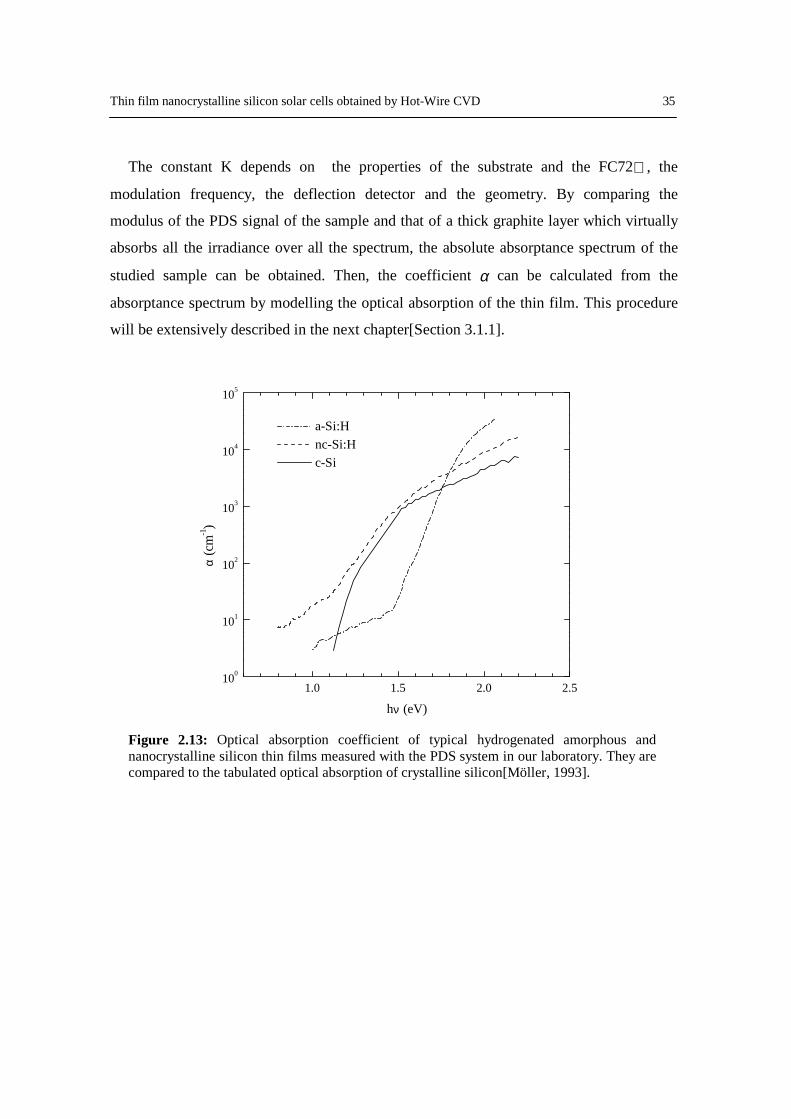
The constant K depends on the properties of the substrate and the FC72 , the
modulation frequency, the deflection detector and the geometry. By comparing the
modulus of the PDS signal of the sample and that of a thick graphite layer which virtually
absorbs all the irradiance over all the spectrum, the absolute absorptance spectrum of the
studied sample can be obtained. Then, the coefficient α can be calculated from the
absorptance spectrum by modelling the optical absorption of the thin film. This procedure
will be extensively described in the next chapter[Section 3.1.1].
1.0 1.5 2.0 2.5100
101
102
103
104
105
a-Si:H nc-Si:H c-Si
hν (eV)
α (c
m-1)
Figure 2.13: Optical absorption coefficient of typical hydrogenated amorphous and nanocrystalline silicon thin films measured with the PDS system in our laboratory. They are compared to the tabulated optical absorption of crystalline silicon[Möller, 1993].
36 The HWCVD set-up. Optical and electrical characterisations
2.3. Characterisation of devices
2.3.1. Current density - voltage characteristics
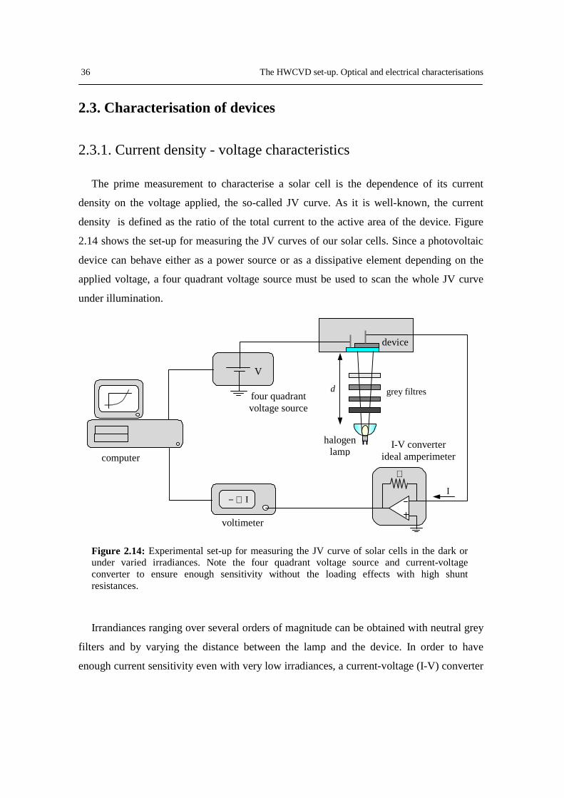
The prime measurement to characterise a solar cell is the dependence of its current
density on the voltage applied, the so-called JV curve. As it is well-known, the current
density is defined as the ratio of the total current to the active area of the device. Figure
2.14 shows the set-up for measuring the JV curves of our solar cells. Since a photovoltaic
device can behave either as a power source or as a dissipative element depending on the
applied voltage, a four quadrant voltage source must be used to scan the whole JV curve
under illumination.
Figure 2.14: Experimental set-up for measuring the JV curve of solar cells in the dark or under varied irradiances. Note the four quadrant voltage source and current-voltage converter to ensure enough sensitivity without the loading effects with high shunt resistances.
Irrandiances ranging over several orders of magnitude can be obtained with neutral grey
filters and by varying the distance between the lamp and the device. In order to have
enough current sensitivity even with very low irradiances, a current-voltage (I-V) converter
device
halogen lamp
four quadrant voltage source
V
voltimeter
ℜ
d
− ℜ I I
computer
grey filtres
I-V converter ideal amperimeter
Thin film nanocrystalline silicon solar cells obtained by Hot-Wire CVD 37
acting as an ideal amperimeter was used. In this way, loading effects related to shunt
resistances are avoided.
JV curve
Power density
Vmp
jmp
Voc
jsc
Voltage
Cur
rent
den
sity
P = V× J
FF =Voc jsc
Vmp jmp
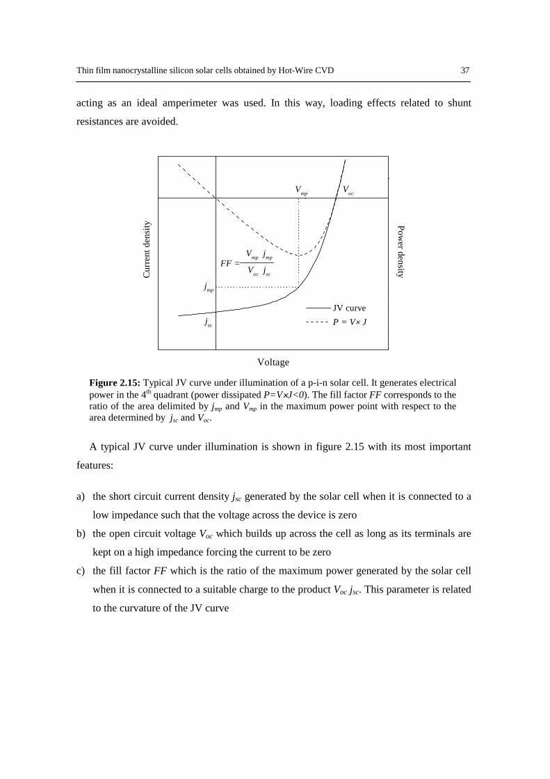
Figure 2.15: Typical JV curve under illumination of a p-i-n solar cell. It generates electrical power in the 4th quadrant (power dissipated P=V×J<0). The fill factor FF corresponds to the ratio of the area delimited by jmp and Vmp in the maximum power point with respect to the area determined by jsc and Voc.
A typical JV curve under illumination is shown in figure 2.15 with its most important
features:
a) the short circuit current density jsc generated by the solar cell when it is connected to a
low impedance such that the voltage across the device is zero
b) the open circuit voltage Voc which builds up across the cell as long as its terminals are
kept on a high impedance forcing the current to be zero
c) the fill factor FF which is the ratio of the maximum power generated by the solar cell
when it is connected to a suitable charge to the product Voc jsc. This parameter is related
to the curvature of the JV curve
38 The HWCVD set-up. Optical and electrical characterisations
The ratio of the electrical power density at the maximum power point to the incident
power density due to illumination is the conversion efficiency of the solar cell η
light
scoc
light
mpmp
light
max
PjV FF
PjV
PP
===η (2.15)
From equation 2.15 it is obvious that in order to get the highest conversion efficiency
from a solar cell the three basic parameters of its JV curve have all to be maximised.
2.3.2. Spectral response and quantum efficiencies
The spectral response of a solar cell SR(V,λ) is given by the ratio of the photogenerated
current jph(V,λ) to the incident power P(λ) spectral densities (magnitudes per unit area and
unit wavelength)[Eq. 2.16]. It indicates, for an external voltage applied V, how much
current in ampers is collected from the device per incident watt of light with wavelength λ
)(),(
),(λ
λλ
PVj
VSR ph= (2.16)
With a more physical meaning it is often used the external quantum efficiency
QEext(V,λ), which is the fraction of incident photons of a given wavelength φo(λ) which
results in an electron-hole pair collected at the contacts of the cell. The external quantum
efficiency is influenced not only by the collection efficiency but also by the optical
optimisation of the device. The spectral response is related to the external quantum
efficiency by equation 2.17, where if SR is in A/W and λ in nm we obtain QEext in e/ph
λλ
λφλ
λ1241),(
)(),(
),( VSRe
VjVQE
o
phext == (2.17)
Figure 2.16 shows the experimental set-up used for the measurements. For accurate
absolute spectral measurements it was necessary to determine the spectral power density
P(λ) incident to the solar cell under test. This was done by placing in the sample holder a
Thin film nanocrystalline silicon solar cells obtained by Hot-Wire CVD 39
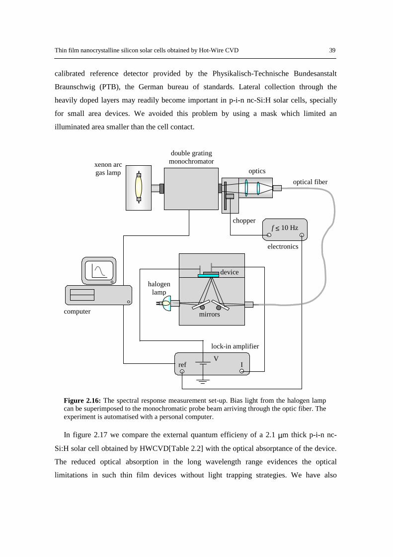
calibrated reference detector provided by the Physikalisch-Technische Bundesanstalt
Braunschwig (PTB), the German bureau of standards. Lateral collection through the
heavily doped layers may readily become important in p-i-n nc-Si:H solar cells, specially
for small area devices. We avoided this problem by using a mask which limited an
illuminated area smaller than the cell contact.
Figure 2.16: The spectral response measurement set-up. Bias light from the halogen lamp can be superimposed to the monochromatic probe beam arriving through the optic fiber. The experiment is automatised with a personal computer.
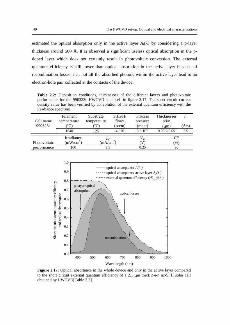
In figure 2.17 we compare the external quantum efficieny of a 2.1 µm thick p-i-n nc-
Si:H solar cell obtained by HWCVD[Table 2.2] with the optical absorptance of the device.
The reduced optical absorption in the long wavelength range evidences the optical
limitations in such thin film devices without light trapping strategies. We have also
computer
lock-in amplifier
I ref
chopper f ≤ 10 Hz
double grating monochromator
electronics
xenon arc gas lamp
optical fiber
mirrors
optics
device
halogen lamp
V
40 The HWCVD set-up. Optical and electrical characterisations
estimated the optical absorption only in the active layer Ai(λ) by considering a p-layer
thickness around 500 Å. It is observed a significant useless optical absorption in the p-
doped layer which does not certainly result in photovoltaic conversion. The external
quantum efficiency is still lower than optical absorption in the active layer because of
recombination losses, i.e., not all the absorbed photons within the active layer lead to an
electron-hole pair collected at the contacts of the device.
Table 2.2: Deposition conditions, thicknesses of the different layers and photovoltaic performance for the 990323c HWCVD solar cell in figure 2.17. The short circuit current density value has been verified by convolution of the external quantum efficiency with the irradiance spectrum.
Filament temperature
(ºC)
Substrate temperature
(ºC)
SiH4/H2 flows
(sccm)
Process pressure (mbar)
Thicknesses p/i/n (µm)
rd
(Å/s)
Cell name 990323c
1640 125 4 / 76 3.5 10-2 0.05/2/0.05 2.5
Irradiance (mW/cm2)
jsc (mA/cm2)
Voc (V)
FF (%)
Photovoltaic performance 100 9.5 0.25 36
400 500 600 700 800 900 10000.0
0.1
0.2
0.3
0.4
0.5
0.6
0.7
0.8
0.9
1.0 optical absorptance A(λ ) optical absorptance active layer Ai (λ ) external quantum efficiency QEext (0,λ )
p-layer optical absorption
recombination
optical losses
Wavelength (nm)
Shor
t circ
uit e
xter
nal q
uant
um e
ffici
ncy
and
optic
al a
bsor
ptan
ce
Figure 2.17: Optical absortance in the whole device and only in the active layer compared to the short circuit external quantum efficiency of a 2.1 µm thick p-i-n nc-Si:H solar cell obtained by HWCVD[Table 2.2].
Thin film nanocrystalline silicon solar cells obtained by Hot-Wire CVD 41
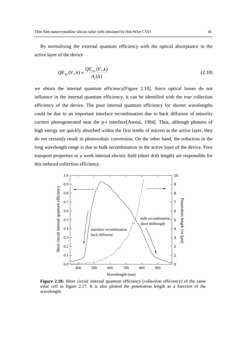
By normalising the external quantum efficiency with the optical absorptance in the
active layer of the device
)(),(
),( extint λ
λλ
iAVQE
VQE = (2.18)
we obtain the internal quantum efficiency[Figure 2.18]. Since optical losses do not
influence in the internal quantum efficiency, it can be identified with the true collection
efficiency of the device. The poor internal quantum efficiency for shorter wavelengths
could be due to an important interface recombination due to back diffusion of minority
carriers photogenerated near the p-i interface[Asensi, 1994]. Thus, although photons of
high energy are quickly absorbed within the first tenths of micron in the active layer, they
do not certainly result in photovoltaic conversion. On the other hand, the reduction in the
long wavelength range is due to bulk recombination in the active layer of the device. Poor
transport properties or a week internal electric field (short drift length) are responsible for
this reduced collection efficiency.
400 500 600 700 800 9000.0
0.1
0.2
0.3
0.4
0.5
0.6
0.7
0.8
0.9
1.0
Wavelength (nm)
Shor
t circ
uit i
nter
nal q
uant
um e
ffici
ency
0
1
2
3
4
5
6
7
8
9
10
interface recombinationback diffusion
bulk recombinationshort driftlength
Penetration length 1/α (µ m)
Figure 2.18: Short circuit internal quantum efficiency (collection efficiency) of the same solar cell in figure 2.17. It is also plotted the penetration length as a function of the wavelength.
42 The HWCVD set-up. Optical and electrical characterisations
2.3.3. Depletion capacitance of rectifying contacts
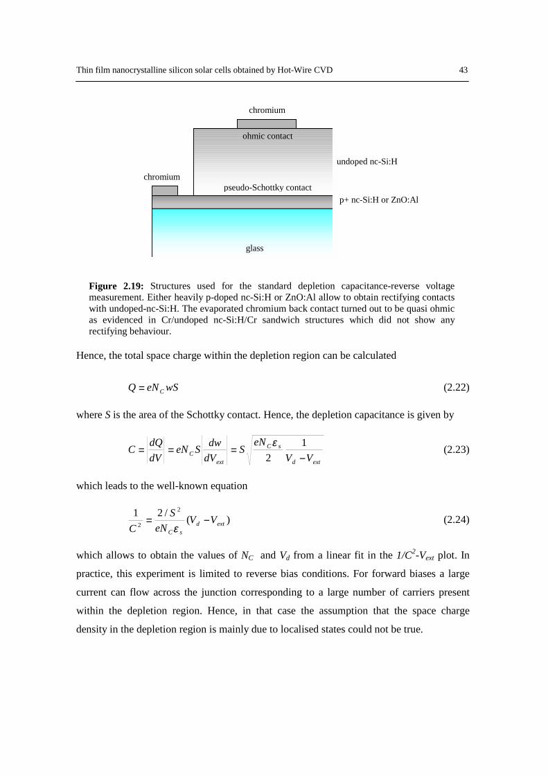
The space charge density in the intrinsic layer of a p-i-n structure screens the internal
electric field of the device thus degrading the drift-assisted collection. Considering the
simplest case of an uniform density of charged centres NC, the Poisson’s equation allows to
calculate the screening length Lscreen of the electric field at the interface Eo arriving at
oC
sscreen E
eNL ε
= (2.19)
where e is the elementary charge and εs the dielectric permitivity of silicon. Then, a
reduction in the densitiy of charged centres would lead to a proportionally longer screening
length and an enhanced drift-assisted collection.
The reverse voltage dependence of the depletion capacitance of Schottky contacts has
been traditionally used to study impurity profiles in crystalline silicon[Rhoderick, 1978].
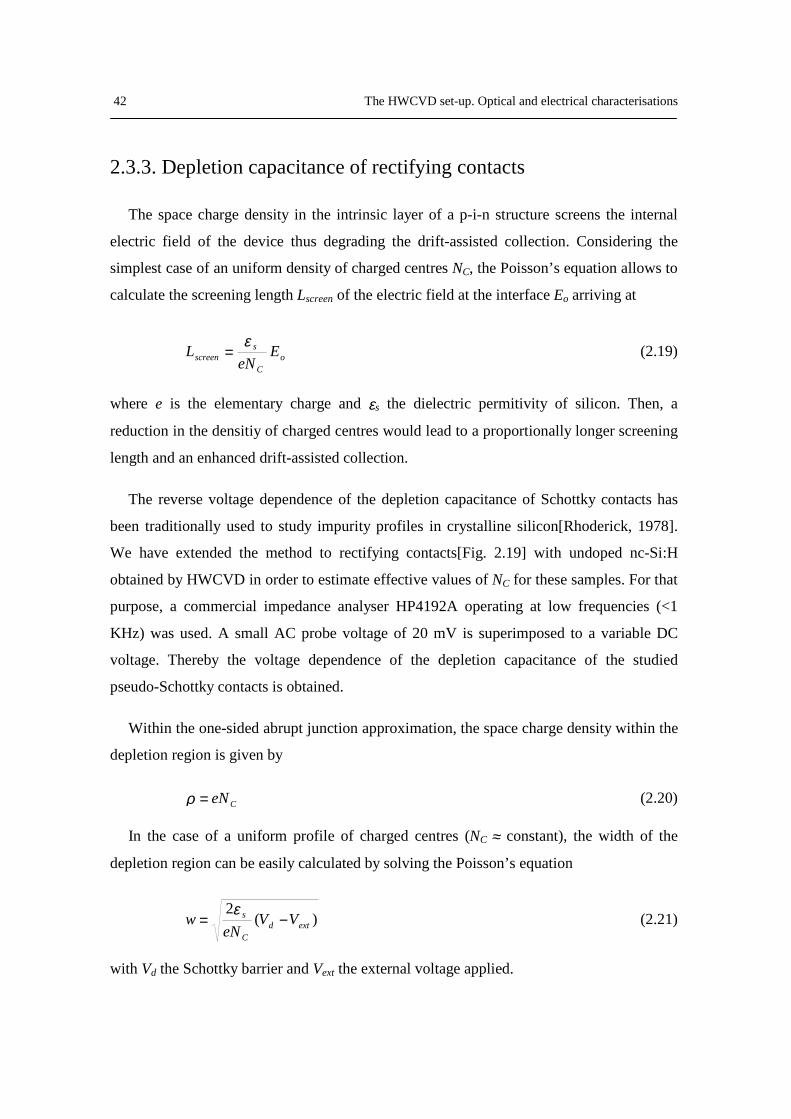
We have extended the method to rectifying contacts[Fig. 2.19] with undoped nc-Si:H
obtained by HWCVD in order to estimate effective values of NC for these samples. For that
purpose, a commercial impedance analyser HP4192A operating at low frequencies (<1
KHz) was used. A small AC probe voltage of 20 mV is superimposed to a variable DC
voltage. Thereby the voltage dependence of the depletion capacitance of the studied
pseudo-Schottky contacts is obtained. Within the one-sided abrupt junction approximation, the space charge density within the
depletion region is given by
CeN=ρ (2.20)
In the case of a uniform profile of charged centres (NC ≈ constant), the width of the
depletion region can be easily calculated by solving the Poisson’s equation
)(2
extdC
s VVeN
w −=ε (2.21)
with Vd the Schottky barrier and Vext the external voltage applied.
Thin film nanocrystalline silicon solar cells obtained by Hot-Wire CVD 43
Figure 2.19: Structures used for the standard depletion capacitance-reverse voltage measurement. Either heavily p-doped nc-Si:H or ZnO:Al allow to obtain rectifying contacts with undoped-nc-Si:H. The evaporated chromium back contact turned out to be quasi ohmic as evidenced in Cr/undoped nc-Si:H/Cr sandwich structures which did not show any rectifying behaviour.
Hence, the total space charge within the depletion region can be calculated
wSeNQ C= (2.22)
where S is the area of the Schottky contact. Hence, the depletion capacitance is given by
extd
sC
extC VV
eNS
dVdwSeN
dVdQC
−===
12
ε (2.23)
which leads to the well-known equation
)(/21 2
2 extdsC
VVeN
SC
−=ε
(2.24)
which allows to obtain the values of NC and Vd from a linear fit in the 1/C2-Vext plot. In
practice, this experiment is limited to reverse bias conditions. For forward biases a large
current can flow across the junction corresponding to a large number of carriers present
within the depletion region. Hence, in that case the assumption that the space charge
density in the depletion region is mainly due to localised states could not be true.
chromium
chromium
undoped nc-Si:H
p+ nc-Si:H or ZnO:Al
glass
ohmic contact
pseudo-Schottky contact
44 The HWCVD set-up. Optical and electrical characterisations
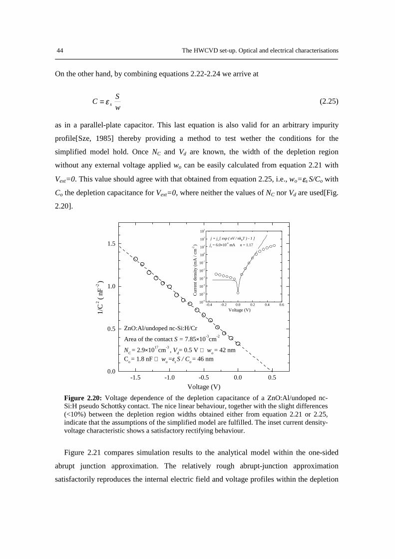
On the other hand, by combining equations 2.22-2.24 we arrive at
wSC sε= (2.25)
as in a parallel-plate capacitor. This last equation is also valid for an arbitrary impurity
profile[Sze, 1985] thereby providing a method to test wether the conditions for the
simplified model hold. Once NC and Vd are known, the width of the depletion region
without any external voltage applied wo can be easily calculated from equation 2.21 with
Vext=0. This value should agree with that obtained from equation 2.25, i.e., wo=εs S/Co with
Co the depletion capacitance for Vext=0, where neither the values of NC nor Vd are used[Fig.
2.20].
-1.5 -1.0 -0.5 0.0 0.50.0
0.5
1.0
1.5
ZnO:Al/undoped nc-Si:H/Cr
Area of the contact S = 7.85×10⁻³cm-2
NC = 2.9×1017cm-3 , Vd= 0.5 V ⇒ wo = 42 nmCo = 1.8 nF ⇒ wo =εs S / Co = 46 nm
Voltage (V)
1/C 2
( nF
-2 )
-0.4 -0.2 0.0 0.2 0.4 0.610-6
10-5
10-4
10-3
10-2
10-1
100
101
102
103
j = jo [ exp ( eV / nkBT ) - 1 ]
jo = 6.0×10⁻⁴ mA n = 1.17
Voltage (V)
Cur
rent
den
sity
(mA
/ cm
-2 )
Figure 2.20: Voltage dependence of the depletion capacitance of a ZnO:Al/undoped nc-Si:H pseudo Schottky contact. The nice linear behaviour, together with the slight differences (<10%) between the depletion region widths obtained either from equation 2.21 or 2.25, indicate that the assumptions of the simplified model are fulfilled. The inset current density-voltage characteristic shows a satisfactory rectifying behaviour.
Figure 2.21 compares simulation results to the analytical model within the one-sided
abrupt junction approximation. The relatively rough abrupt-junction approximation
satisfactorily reproduces the internal electric field and voltage profiles within the depletion
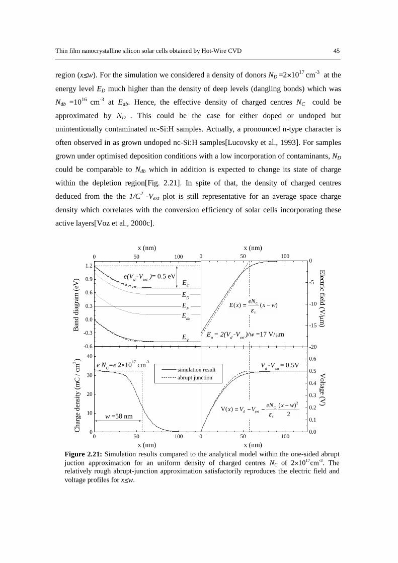
Thin film nanocrystalline silicon solar cells obtained by Hot-Wire CVD 45
region (x≤w). For the simulation we considered a density of donors ND =2×1017 cm-3 at the
energy level ED much higher than the density of deep levels (dangling bonds) which was
Ndb =1016 cm-3 at Edb. Hence, the effective density of charged centres NC could be
approximated by ND . This could be the case for either doped or undoped but
unintentionally contaminated nc-Si:H samples. Actually, a pronounced n-type character is
often observed in as grown undoped nc-Si:H samples[Lucovsky et al., 1993]. For samples
grown under optimised deposition conditions with a low incorporation of contaminants, ND
could be comparable to Ndb which in addition is expected to change its state of charge
within the depletion region[Fig. 2.21]. In spite of that, the density of charged centres
deduced from the the 1/C2 -Vext plot is still representative for an average space charge
density which correlates with the conversion efficiency of solar cells incorporating these
active layers[Voz et al., 2000c].
Figure 2.21: Simulation results compared to the analytical model within the one-sided abrupt juction approximation for an uniform density of charged centres NC of 2×1017cm-3. The relatively rough abrupt-junction approximation satisfactorily reproduces the electric field and voltage profiles for x≤w.
-0.6
-0.3
0.0
0.3
0.6
0.9
1.20 50 100
Vd -Vext = 0.5V
e(Vd -Vext )= 0.5 eV
Edb
x (nm)
x (nm)x (nm)
x (nm)
Char
ge d
ensit
y (m
C / c
m3 )
Voltage (V
)Electric field (V
/µ m)
Ba
nd d
iagr
am (e
V)
0 50 1000
10
20
30
40
e NC=e 2×1017 cm-3
w =58 nm
0 50 100
-20
-15
-10
-5
0
EF
ED
EV
EC
Eo = 2(Vd -Vext )/w =17 V/µm
0 50 1000.0
0.1
0.2
0.3
0.4
0.5
0.6
simulation result abrupt junction
)()( wxeNxEs
C −=ε
2)()(V
2wxeNVVxs
Cextd
−−−=ε

46 The HWCVD set-up. Optical and electrical characterisations
Thin film nanocrystalline silicon solar cells obtained by Hot-Wire CVD 47
Chapter 3 Nanocrystalline silicon by HWCVD: optical and electrical properties
In this chapter we will study the optical and electrical properties of nanocrystalline
silicon obtained by HWCVD. Special attention will be paid to those properties which
clearly influence the photovoltaic performance of devices. The influence of the deposition
conditions on the photovoltaic suitability of the material is also discussed.
3.1. Optical properties
3.1.1. Optical absorption coefficient
A semiconductor suitable for photovoltaic applications should absorb most of the
incident power due to illumination. Not only the optical absorption coefficient α and
optical gap Eg matter, but also the refractive index n, which determines reflection losses.
Figure 3.1 shows an absorbing thin film on its substrate. From the incident power density I
(irradiance), a fraction R (reflectance) is reflected whereas T (transmittance) is transmitted.
Hence, the irradiance fraction A absorbed within the film (absorptance) is
RTA −−=1 (3.1)
Reflection and transmission can be easily measured with a standard spectrophotometer.
However, confident values of the optical absorption coefficient can only be obtained for
high optical absorption (αd >>1) from the transmittance and reflectance spectra only. For
medium or low optical absorption it is necessary to directly measure the optical absorption
within the film which is not so easy. The Photothermal Deflection Spectroscopy (PDS)
[Section 2.2.3][Jackson et al., 1981] or the Constant Photocurrent Method (CPM)[Vanecek
et al., 1983] are well-known techniques with high sensitivity for this purpose.
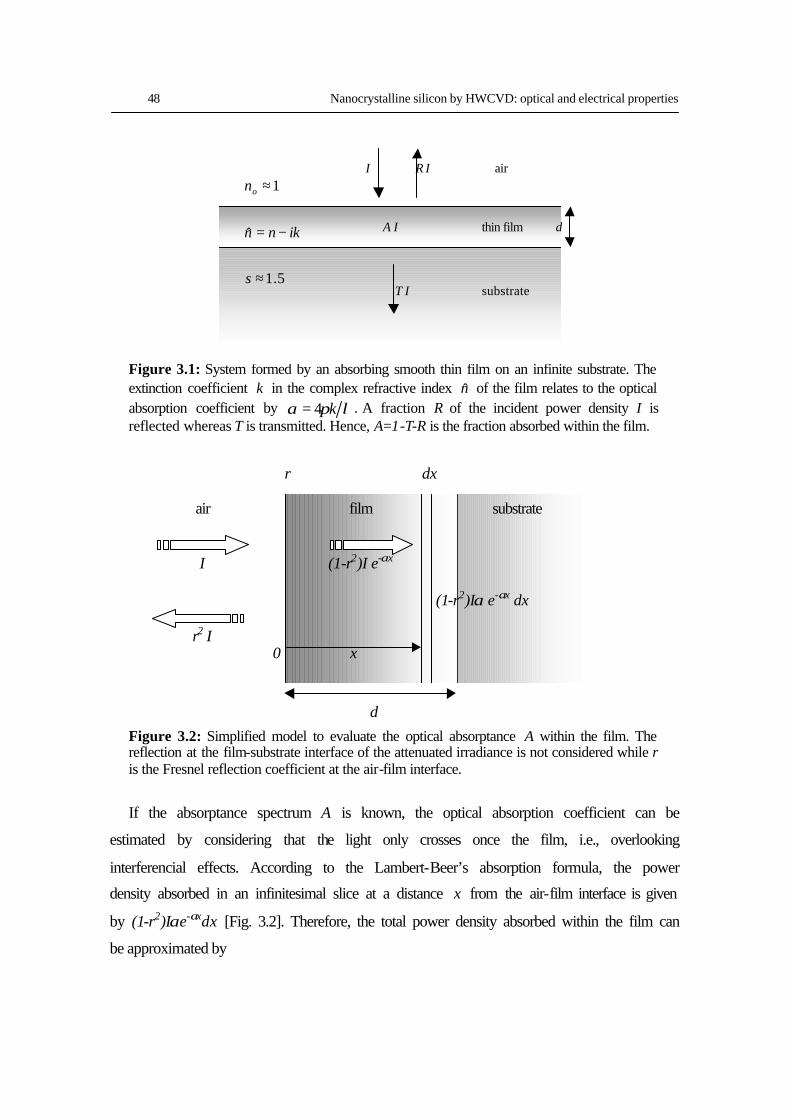
48 Nanocrystalline silicon by HWCVD: optical and electrical properties
Figure 3.1: System formed by an absorbing smooth thin film on an infinite substrate. The extinction coefficient k in the complex refractive index n of the film relates to the optical absorption coefficient by λπα k4= . A fraction R of the incident power density I is reflected whereas T is transmitted. Hence, A=1-T-R is the fraction absorbed within the film.
Figure 3.2: Simplified model to evaluate the optical absorptance A within the film. The reflection at the film-substrate interface of the attenuated irradiance is not considered while r is the Fresnel reflection coefficient at the air-film interface.
If the absorptance spectrum A is known, the optical absorption coefficient can be
estimated by considering that the light only crosses once the film, i.e., overlooking
interferencial effects. According to the Lambert-Beer’s absorption formula, the power
density absorbed in an infinitesimal slice at a distance x from the air-film interface is given
by (1-r2)Iαe-αxdx [Fig. 3.2]. Therefore, the total power density absorbed within the film can
be approximated by
r dx air film substrate I (1-r2)I e-αx (1-r2)Iα e-αx dx r2 I 0 x d
I R I air A I thin film d T I substrate
5.1
ˆ
1
≈
−=
≈
s
iknn
no
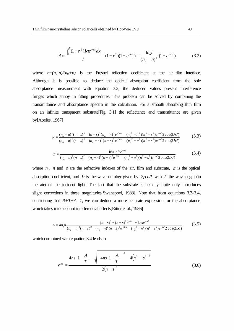
Thin film nanocrystalline silicon solar cells obtained by Hot-Wire CVD 49
)1()(
4)1)(1(
)1(2
20
2
d
o
od
d x
ennnn
erI
dxeIrA αα
αα−−
−
−+
=−−=−
≈ ∫ (3.2)
where r=(no-n)/(no+n) is the Fresnel reflection coefficient at the air -film interface.
Although it is possible to deduce the optical absorption coefficient from the sole
absorptance measurement with equation 3.2, the deduced values present interference
fringes which annoy in fitting procedures. This problem can be solved by combining the
transmittance and absorptance spectra in the calculation. For a smooth absorbing thin film
on an infinite transparent substrate[Fig. 3.1] the reflectance and transmittance are given
by[Abelès, 1967]
)2cos(2))(()()()()(
)2cos(2))(()()()()(222222222
222222222
desnnnesnnnsnnn
desnnnennsnsnnnR
do
doo
do
doo
ββ
αα
αα
−−
−−
−−+−−+++−−++−++−= (3.3)
)2cos(2))(()()()()(
16222222222
2
desnnnesnnnsnnnsenn
Td
od
oo
do
βαα
α
−−
−
−−+−−+++= (3.4)
where no, n and s are the refractive indexes of the air, film and substrate, α is the optical
absorption coefficient, and β is the wave number given by 2π n/λ with λ the wavelength (in
the air) of the incident light. The fact that the substrate is actually finite only introduces
slight corrections in these magnitudes[Swanepoel, 1983]. Note that from equations 3.3-3.4,
considering that R+T+A=1, we can deduce a more accurate expression for the absorptance
which takes into account interferencial effects[Ritter et al., 1986]
)2cos(2))(()()()()(
4)()(4
222222222
222
desnnnesnnnsnnnnseesnsn
nnAd
od
oo
dd
o βαα
αα
−−
−−
−−+−−+++−−−+= (3.5)
which combined with equation 3.4 leads to
( )( )2
222
2
2
414 14
sn
snTA
nsTA
ns
e d
+
−+
++
+
=α (3.6)
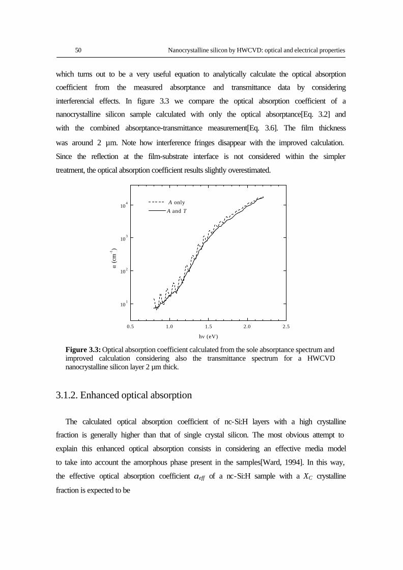
50 Nanocrystalline silicon by HWCVD: optical and electrical properties
which turns out to be a very useful equation to analytically calculate the optical absorption
coefficient from the measured absorptance and transmittance data by considering
interferencial effects. In figure 3.3 we compare the optical absorption coefficient of a
nanocrystalline silicon sample calculated with only the optical absorptance[Eq. 3.2] and
with the combined absorptance-transmittance measurement[Eq. 3.6]. The film thickness
was around 2 µm. Note how interference fringes disappear with the improved calculation.
Since the reflection at the film-substrate interface is not considered within the simpler
treatment, the optical absorption coefficient results slightly overestimated.
0.5 1.0 1.5 2.0 2.5
101
102
103
104 A only
A and T
hν (eV)
α (c
m-1)
Figure 3.3: Optical absorption coefficient calculated from the sole absorptance spectrum and improved calculation considering also the transmittance spectrum for a HWCVD nanocrystalline silicon layer 2 µm thick.
3.1.2. Enhanced optical absorption
The calculated optical absorption coefficient of nc-Si:H layers with a high crystalline
fraction is generally higher than that of single crystal silicon. The most obvious attempt to
explain this enhanced optical absorption consists in considering an effective media model
to take into account the amorphous phase present in the samples[Ward, 1994]. In this way,
the effective optical absorption coefficient αeff of a nc-Si:H sample with a XC crystalline
fraction is expected to be
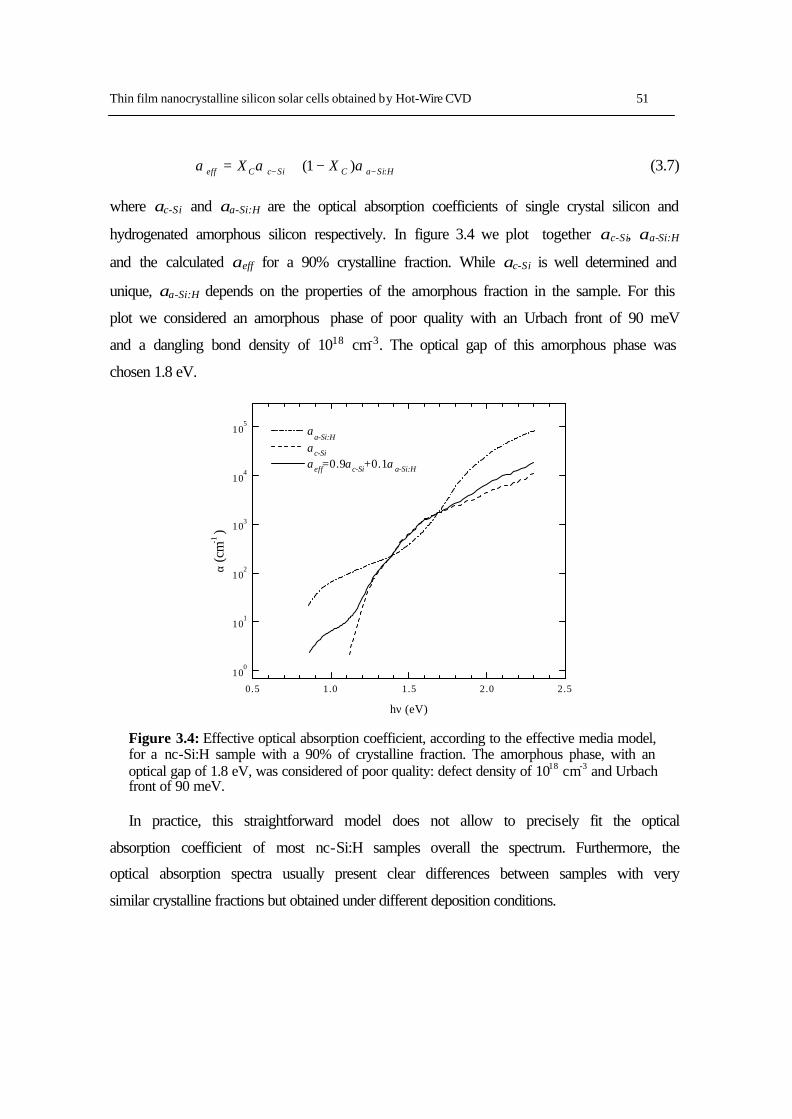
Thin film nanocrystalline silicon solar cells obtained by Hot-Wire CVD 51
HSiaCSicCeff XX :)1( −− −+= ααα (3.7)
where αc-Si and αa-Si:H are the optical absorption coefficients of single crystal silicon and
hydrogenated amorphous silicon respectively. In figure 3.4 we plot together αc-Si, αa-Si:H
and the calculated αeff for a 90% crystalline fraction. While αc-Si is well determined and
unique, αa-Si:H depends on the properties of the amorphous fraction in the sample. For this
plot we considered an amorphous phase of poor quality with an Urbach front of 90 meV
and a dangling bond density of 1018 cm-3. The optical gap of this amorphous phase was
chosen 1.8 eV.
0.5 1.0 1.5 2.0 2.5
100
101
102
103
104
105
αa-Si:H
αc-Si
αeff=0.9αc-Si+0.1αa-Si:H
hν (eV)
α (c
m-1 )
Figure 3.4: Effective optical absorption coefficient, according to the effective media model, for a nc-Si:H sample with a 90% of crystalline fraction. The amorphous phase, with an optical gap of 1.8 eV, was considered of poor quality: defect density of 1018 cm-3 and Urbach front of 90 meV. In practice, this straightforward model does not allow to precisely fit the optical
absorption coefficient of most nc-Si:H samples overall the spectrum. Furthermore, the
optical absorption spectra usually present clear differences between samples with very
similar crystalline fractions but obtained under different deposition conditions.
52 Nanocrystalline silicon by HWCVD: optical and electrical properties
Table 3.1: HWCVD nc-Si:H samples obtained at different process pressures. Both were obtained with a substrate temperature of 150ºC and a 95% hydrogen dilution (4 sccm of SiH4 mixed with 76 sccm of H2). The wire was heated to 1700ºC.
Sample Process pressure (mbar)
Thickness (µm)
rd (Å/s)
Eg (eV)
α(1.5 eV) (cm-1)
LP 7 10-3 1.8 2.4 1.16 611 HP 3.5 10-2 2.1 8.7 1.12 1066
0.5 1.0 1.5 2.0 2.5
1
10
100
1000
10000
mechanical strain?
quantum effects?
surface light
scattering
bulk and surface
light scattering
2
αHP
αL P
αeff
αHP
/αeff
αL P/αeff
hν (eV)
α (c
m-1 )
Figure 3.5: Optical absorption coefficients measured by PDS for the HWCVD nc-Si:H samples in table 3.1. It is also shown the effective optical absorption coefficient expected for a 90% crystalline fraction. The corresponding ratios are also plotted as a measure of the optical absorption enhancement.
In figure 3.5 we show the optical absorption coefficient spectra of two HWCVD nc-Si:H
samples. They were obtained at clearly different process pressures while the rest of
deposition conditions remained unchanged[Table 3.1]. Both samples presented very similar
crystalline fractions around 90% deduced from their Raman spectra[Peiró, 1999]. Hence, an
effective optical absorption αeff was calculated with XC=0.9 in equation 3.7 and plotted
together with the optical absorption coefficients αLP and αHP of the studied samples for
Thin film nanocrystalline silicon solar cells obtained by Hot-Wire CVD 53
comparison. The ratios αLP/αeff and αHP/αeff (≥1) are a direct measurement of the enhanced
optical absorption. Three different regions can be easily distinguished:
a) hν<1.2 eV (λ>1000 nm): It is generally accepted that the subgap optical absorption is
due to deep states in the gap. Hence, the density of dangling bonds could be determined
by deconvoluting this part of the absorption coefficient spectrum[Jackson et al., 1982].
Though this is true in the case of smooth and homogeneous a-Si:H layers, for nc-Si:H
layers the absorption coefficient is greatly influenced by light scattering either at the
surface or in the bulk of the layer [Beck et al., 1998]. Therefore, though this part could
be certainly fitted by properly choosing the defect density in the amorphous phase, the
obtained densities of deep states in the gap could result highly overestimated.
b) 1.2 eV<hν<1.8 eV (1000 nm<λ<700 nm):In this region the optical absorption
coefficient of the HP sample is clearly higher than that of the LP sample. It is observed
that αLP≈αeff whereas αHP≈1.75αeff. A careful optical study with VHF-PECVD nc-Si:H
samples [Poruba et al., 1998] shows that enhanced optical absorption in this part of the
spectrum is undoubtedly due to light scattering at the surface of the films. It was
observed that after chemomechanically polishing the samples up to a mirror-like surface,
the enhanced optical absorption disappeared in this region. We deduce that the HP
sample presented a much rougher surface than the LP sample, which was optically
smooth for this wavelength interval.
c) hν>1.8 eV (λ<700 nm): In the visible region the optical absorption coefficients of
both samples coincide in a value higher than expected according to their measured
crystalline fractions (αHP≈αLP≈1.5αeff). The amorphous phase, which was taken into
account with the effective media approximation[Eq. 3.7], does not allow to explain the
enhanced optical absorption in the visible region. Neither light scattering can explain
this enhanced optical absorption because rough and smooth samples behave here in the
same way. It has been proposed that either strong mechanical strain causing a relaxation
in the kr
selection rule[Schroop et al., 1998] or quantum effects related to the grain
54 Nanocrystalline silicon by HWCVD: optical and electrical properties
size[Kalkan et al.,1997] could be responsible for the enhanced optical absorption in this
part of the spectrum. Furthermore, correlations with the hydrogen content have been also
detected by stepwise annealing the samples[Beck et al., 1996].
3.1.3. Benefits from enhanced optical absorption
While optical absorption in the subgap region is not interesting for photovoltaic
applications, absorbed photons of energy over the band gap certainly photogenerate useful
electron-hole pairs. Then, however it is caused, enhanced optical absorption for photon
energies higher than the band gap is advantageous for photovoltaic applications. In figure
3.6 we compare the optical absorptances AHP and ALP expected for 2 µm thick films with
the optical absorption coefficient spectra αHP and αLP in figure 3.5, respectively. A
thickness of 2 µm was choosen for the calculation because it is in the order of the thickness
of the active layer in a p-i-n nc-Si:H solar cell. We observe that 2 µm thick films are
already optically dense in the visible part of the spectrum. Therefore, though there is some
optical absorption enhancement there, it would not supose a great improvement in the solar
cell performance. By contrast, enhanced absorption in the near infrared certainly results in
an advantageos gain of photogeneration. Under AM1.5 irradiance conditions, the maximum
current density generated in such layers can be calculated as
λλλλλ∫<
=o
dAJj AMmax )()(5.1 (3.8)
where A(λ) is the absorptance spectrum related to the optical absorption coefficient
spectrum α(λ) by equation 3.2. The integral extends over the wavelength interval λ<λo
where λo=hc/Eg, i.e., for photon energies higher than the band gap. For simplicity, in
equation 3.8 the AM1.5 spectrum JAM1.5(λ) is in current density units (mA cm-2 nm-1)
assuming one electron-hole pair generated per absorbed photon. That is
)(1241
)( 5.15.1 λλ
λ AMAM PJ = (3.9)
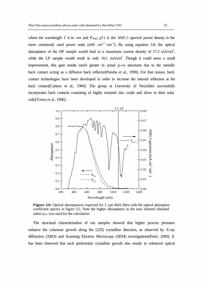
Thin film nanocrystalline silicon solar cells obtained by Hot-Wire CVD 55
where the wavelenght λ is in nm and PAM1.5(λ) is the AM1.5 spectral power density in the
more commonly used power units (mW cm-2 nm-1). By using equation 3.8, the optical
absorptance of the HP sample would lead to a maximum current density of 17.2 mA/cm2,
while the LP sample would result in only 16.1 mA/cm2. Though it could seem a small
improvement, this gain results much greater in actual p-i-n structures due to the metallic
back contact acting as a diffusive back reflector[Poruba et al., 1998]. For that reason, back
contact technologies have been developed in order to increase the internal reflection at the
back contact[Carlson et al., 1984]. The group at University of Neuchâtel successfully
incorporates back contacts consisting of highly textured zinc oxide and silver in their solar
cells[Torres et al., 1996].
200 400 600 800 1000 1200 14000.0
0.1
0.2
0.3
0.4
0.5
0.6
0.7
0.8
0.9
1.01.1 eV
AH P A
L P
Wavelength (nm)
Abs
orpt
ance
0.00
0.01
0.02
0.03
0.04
0.05
0.06
0.07
0.08
JAM1.5
AM
1.5 spectrum (m
A cm
-2 nm-1 )
Figure 3.6: Optical absorptances expected for 2 µm thick films with the optical absorption coefficient spectra in figure 3.5. Note the higher absorptance in the near infrared obtained when αHP was used for the calculation.
The structural characterisation of our samples showed that higher process pressures
enhance the columnar growth along the [220] crystalline direction, as observed by X-ray
diffraction (XRD) and Scanning Electron Microscopy (SEM) investigations[Peiró, 2000]. It
has been observed that such preferential crystalline growth also results in enhanced optical
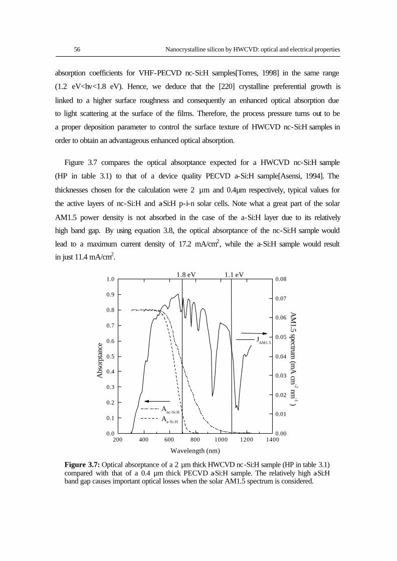
56 Nanocrystalline silicon by HWCVD: optical and electrical properties
absorption coefficients for VHF-PECVD nc-Si:H samples[Torres, 1998] in the same range
(1.2 eV<hν<1.8 eV). Hence, we deduce that the [220] crystalline preferential growth is
linked to a higher surface roughness and consequently an enhanced optical absorption due
to light scattering at the surface of the films. Therefore, the process pressure turns out to be
a proper deposition parameter to control the surface texture of HWCVD nc-Si:H samples in
order to obtain an advantageous enhanced optical absorption.
Figure 3.7 compares the optical absorptance expected for a HWCVD nc-Si:H sample
(HP in table 3.1) to that of a device quality PECVD a-Si:H sample[Asensi, 1994]. The
thicknesses chosen for the calculation were 2 µm and 0.4µm respectively, typical values for
the active layers of nc-Si:H and a-Si:H p-i-n solar cells. Note what a great part of the solar
AM1.5 power density is not absorbed in the case of the a-Si:H layer due to its relatively
high band gap. By using equation 3.8, the optical absorptance of the nc-Si:H sample would
lead to a maximum current density of 17.2 mA/cm2, while the a-Si:H sample would result
in just 11.4 mA/cm2.
200 400 600 800 1000 1200 14000.0
0.1
0.2
0.3
0.4
0.5
0.6
0.7
0.8
0.9
1.0
AM
1.5 spectrum (m
A cm
-2 nm-1 )
1.8 eV 1.1 eV
Anc-Si:H
Aa-Si:H
Wavelength (nm)
Abs
orpt
ance
0.00
0.01
0.02
0.03
0.04
0.05
0.06
0.07
0.08
JAM1.5
Figure 3.7: Optical absorptance of a 2 µm thick HWCVD nc-Si:H sample (HP in table 3.1) compared with that of a 0.4 µm thick PECVD a-Si:H sample. The relatively high a-Si:H band gap causes important optical losses when the solar AM1.5 spectrum is considered.
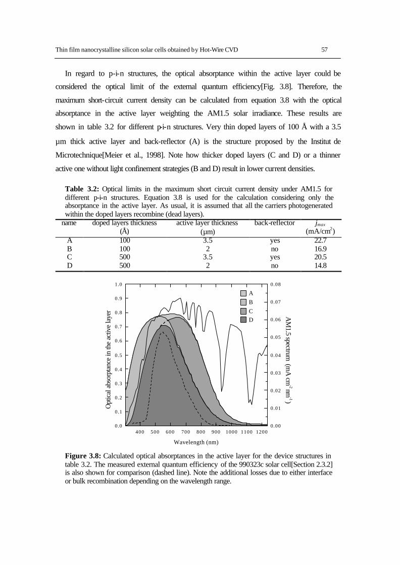
Thin film nanocrystalline silicon solar cells obtained by Hot-Wire CVD 57
In regard to p-i-n structures, the optical absorptance within the active layer could be
considered the optical limit of the external quantum efficiency[Fig. 3.8]. Therefore, the
maximum short-circuit current density can be calculated from equation 3.8 with the optical
absorptance in the active layer weighting the AM1.5 solar irradiance. These results are
shown in table 3.2 for different p-i-n structures. Very thin doped layers of 100 Å with a 3.5
µm thick active layer and back-reflector (A) is the structure proposed by the Institut de
Microtechnique[Meier et al., 1998]. Note how thicker doped layers (C and D) or a thinner
active one without light confinement strategies (B and D) result in lower current densities.
Table 3.2: Optical limits in the maximum short circuit current density under AM1.5 for different p-i-n structures. Equation 3.8 is used for the calculation considering only the absorptance in the active layer. As usual, it is assumed that all the carriers photogenerated within the doped layers recombine (dead layers).
name doped layers thickness (Å)
active layer thickness (µm)
back-reflector jmax (mA/cm2)
A 100 3.5 yes 22.7 B 100 2 no 16.9 C 500 3.5 yes 20.5 D 500 2 no 14.8
400 500 600 700 800 900 1000 1100 12000.0
0.1
0.2
0.3
0.4
0.5
0.6
0.7
0.8
0.9
1.0
A
B
CD
Wavelength (nm)
Opt
ical
abs
orpt
ance
in th
e ac
tive
laye
r
0.00
0.01
0.02
0.03
0.04
0.05
0.06
0.07
0.08
AM
1.5 spectrum (m
A cm
-2 nm-1 )
Figure 3.8: Calculated optical absorptances in the active layer for the device structures in table 3.2. The measured external quantum efficiency of the 990323c solar cell[Section 2.3.2] is also shown for comparison (dashed line). Note the additional losses due to either interface or bulk recombination depending on the wavelength range.
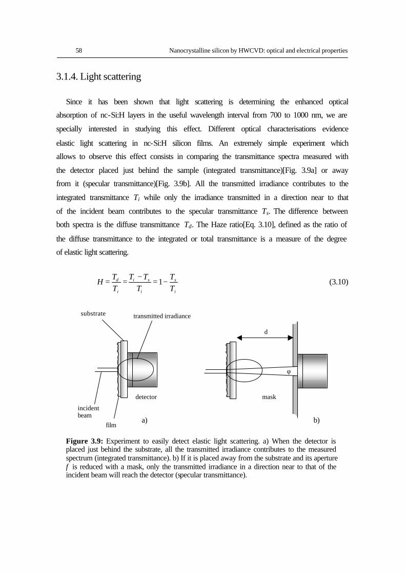
58 Nanocrystalline silicon by HWCVD: optical and electrical properties
3.1.4. Light scattering
Since it has been shown that light scattering is determining the enhanced optical
absorption of nc-Si:H layers in the useful wavelength interval from 700 to 1000 nm, we are
specially interested in studying this effect. Different optical characterisations evidence
elastic light scattering in nc-Si:H silicon films. An extremely simple experiment which
allows to observe this effect consists in comparing the transmittance spectra measured with
the detector placed just behind the sample (integrated transmittance)[Fig. 3.9a] or away
from it (specular transmittance)[Fig. 3.9b]. All the transmitted irradiance contributes to the
integrated transmittance Ti while only the irradiance transmitted in a direction near to that
of the incident beam contributes to the specular transmittance Ts. The difference between
both spectra is the diffuse transmittance Td. The Haze ratio[Eq. 3.10], defined as the ratio of
the diffuse transmittance to the integrated or total transmittance is a measure of the degree
of elastic light scattering.
i
s
i
si
i
d
TT
TTT
TT
H −=−== 1 (3.10)
Figure 3.9: Experiment to easily detect elastic light scattering. a) When the detector is placed just behind the substrate, all the transmitted irradiance contributes to the measured spectrum (integrated transmittance). b) If it is placed away from the substrate and its aperture φ is reduced with a mask, only the transmitted irradiance in a direction near to that of the incident beam will reach the detector (specular transmittance).
substrate
incident beam
film
transmitted irradiance
detector mask
d φ
a) b)
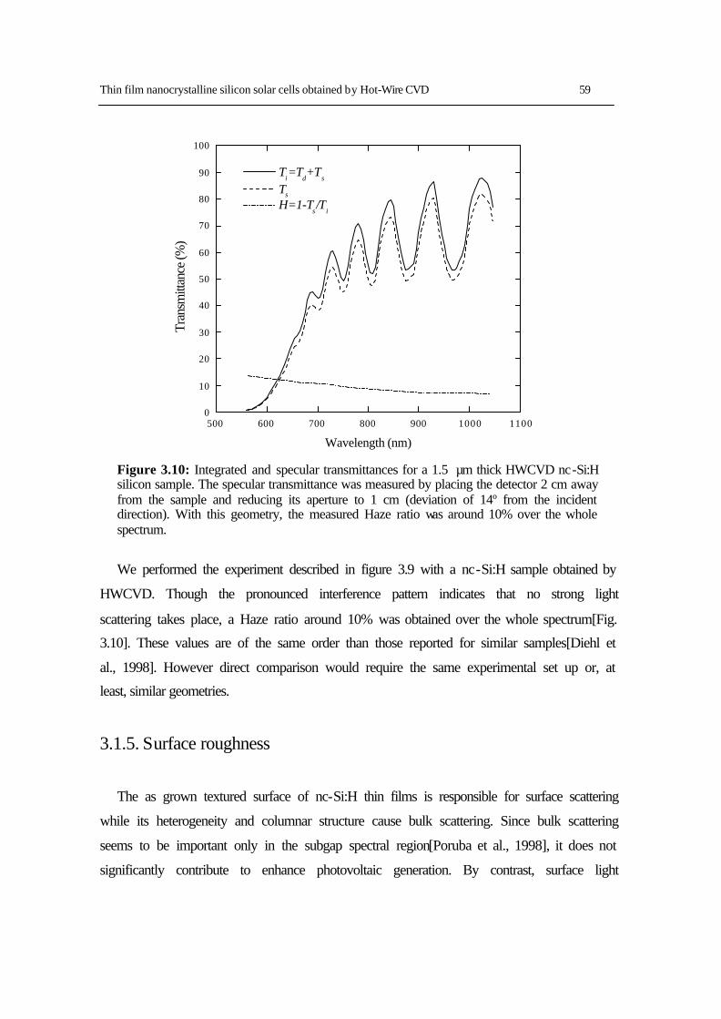
Thin film nanocrystalline silicon solar cells obtained by Hot-Wire CVD 59
500 600 700 800 900 1000 11000
10
20
30
40
50
60
70
80
90
100
Ti=T
d+T
s
Ts
H=1-Ts/T
i
Wavelength (nm)
Tran
smitt
ance
(%)
Figure 3.10: Integrated and specular transmittances for a 1.5 µm thick HWCVD nc-Si:H silicon sample. The specular transmittance was measured by placing the detector 2 cm away from the sample and reducing its aperture to 1 cm (deviation of 14º from the incident direction). With this geometry, the measured Haze ratio was around 10% over the whole spectrum.
We performed the experiment described in figure 3.9 with a nc-Si:H sample obtained by
HWCVD. Though the pronounced interference pattern indicates that no strong light
scattering takes place, a Haze ratio around 10% was obtained over the whole spectrum[Fig.
3.10]. These values are of the same order than those reported for similar samples[Diehl et
al., 1998]. However direct comparison would require the same experimental set up or, at
least, similar geometries.
3.1.5. Surface roughness
The as grown textured surface of nc-Si:H thin films is responsible for surface scattering
while its heterogeneity and columnar structure cause bulk scattering. Since bulk scattering
seems to be important only in the subgap spectral region[Poruba et al., 1998], it does not
significantly contribute to enhance photovoltaic generation. By contrast, surface light
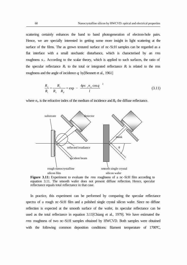
60 Nanocrystalline silicon by HWCVD: optical and electrical properties
scattering certainly enhances the band to band photogeneration of electron-hole pairs.
Hence, we are specially interested in getting some more insight in light scattering at the
surface of the films. The as grown textured surface of nc-Si:H samples can be regarded as a
flat interface with a small stochastic disturbance, which is characterised by an rms
roughness σr. According to the scalar theory, which is applied to such surfaces, the ratio of
the specular reflectance Rs to the total or integrated reflectance Ri is related to the rms
roughness and the angle of incidence θ by[Bennett et al., 1961]
−=
+=
2cos4
expλ
θπσ or
ds
s
i
s n
RR
R
R
R (3.11)
where no is the refractive index of the medium of incidence and Rd the diffuse reflectance.
Figure 3.11: Experiment to evaluate the rms roughness of a nc-Si:H film according to equation 3.11. The smooth wafer does not present diffuse reflection. Hence, specular reflectance equals total reflectance in that case.
In practice, this experiment can be performed by comparing the specular reflectance
spectra of a rough nc-Si:H film and a polished single crystal silicon wafer. Since no diffuse
reflection is expected at the smooth surface of the wafer, its specular reflectance can be
used as the total reflectance in equation 3.11[Chiang et al., 1979]. We have estimated the
rms roughness of two nc-Si:H samples obtained by HWCVD. Both samples were obtained
with the following common deposition conditions: filament temperature of 1700ºC,
substrate detector mask reflected irradiance θ incident beam rough nanocrystalline smooth single crystal
silicon film silicon wafer
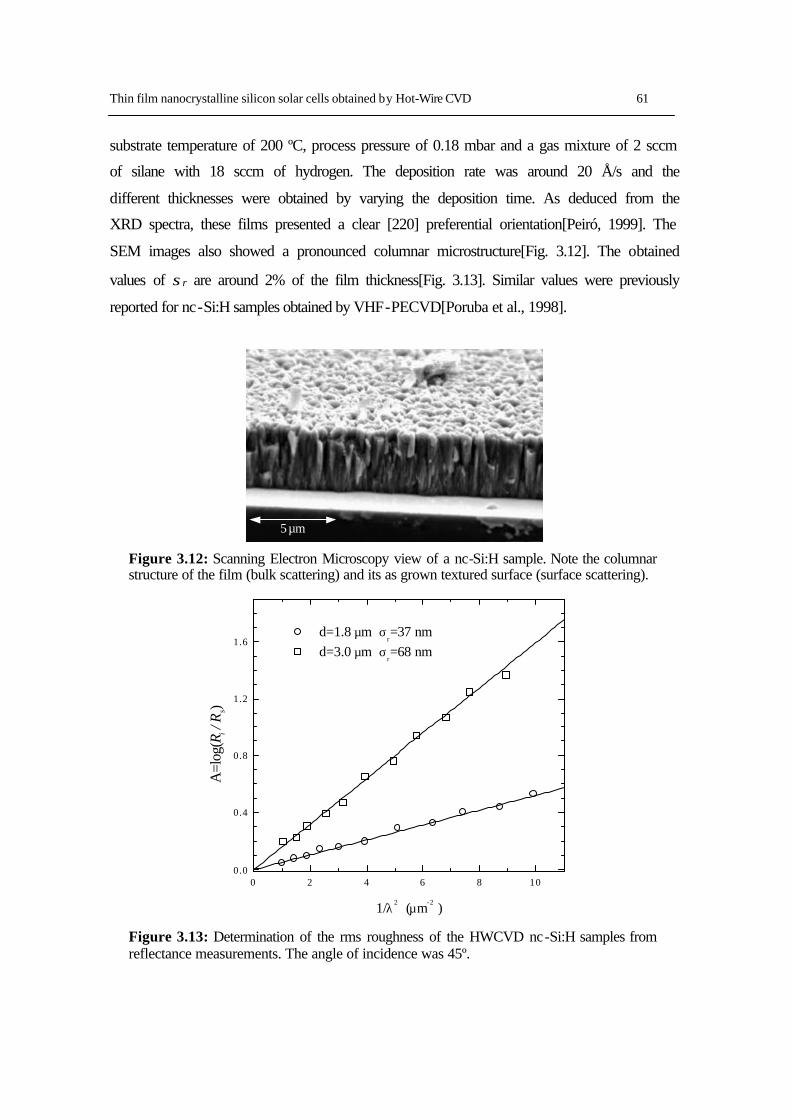
Thin film nanocrystalline silicon solar cells obtained by Hot-Wire CVD 61
substrate temperature of 200 ºC, process pressure of 0.18 mbar and a gas mixture of 2 sccm
of silane with 18 sccm of hydrogen. The deposition rate was around 20 Å/s and the
different thicknesses were obtained by varying the deposition time. As deduced from the
XRD spectra, these films presented a clear [220] preferential orientation[Peiró, 1999]. The
SEM images also showed a pronounced columnar microstructure[Fig. 3.12]. The obtained
values of σr are around 2% of the film thickness[Fig. 3.13]. Similar values were previously
reported for nc-Si:H samples obtained by VHF-PECVD[Poruba et al., 1998].
Figure 3.12: Scanning Electron Microscopy view of a nc-Si:H sample. Note the columnar structure of the film (bulk scattering) and its as grown textured surface (surface scattering).
0 2 4 6 8 100.0
0.4
0.8
1.2
1.6 d=1.8 µm σ
r=37 nm
d=3.0 µm σr=68 nm
1/λ2 (µm-2 )
A=l
og(R
i / R
s)
Figure 3.13: Determination of the rms roughness of the HWCVD nc-Si:H samples from reflectance measurements. The angle of incidence was 45º.
5 µm
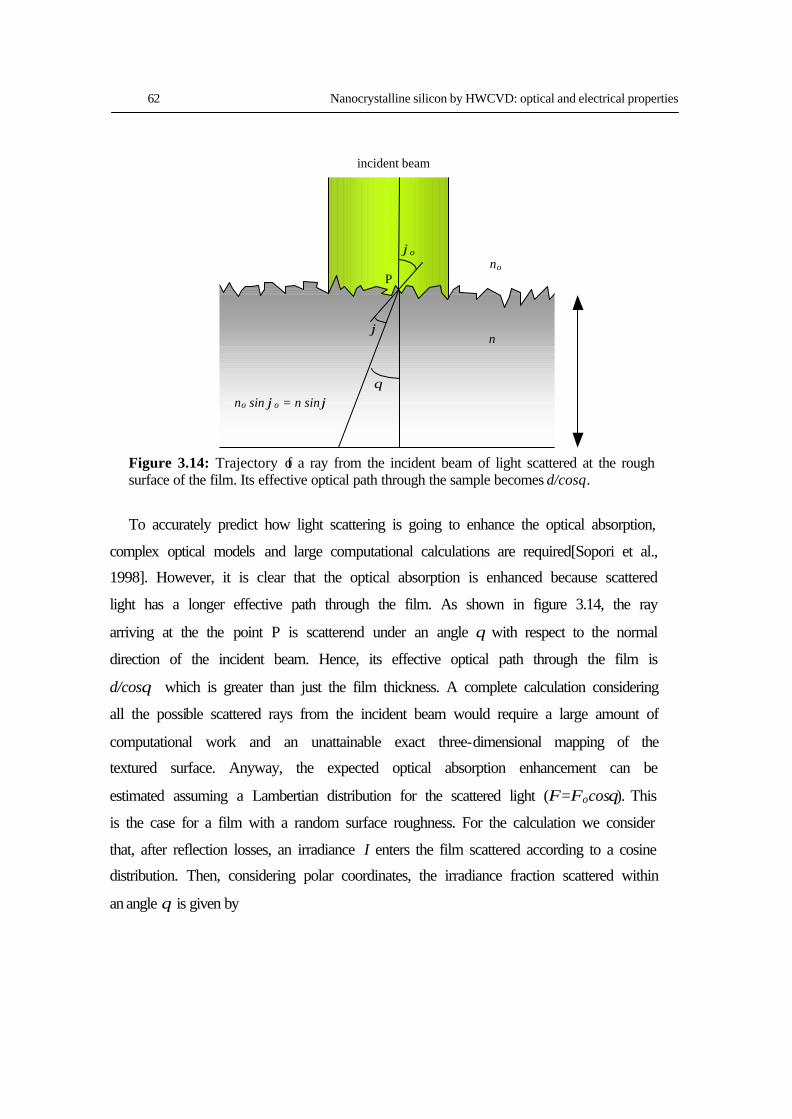
62 Nanocrystalline silicon by HWCVD: optical and electrical properties
Figure 3.14: Trajectory of a ray from the incident beam of light scattered at the rough surface of the film. Its effective optical path through the sample becomes d/cosθ.
To accurately predict how light scattering is going to enhance the optical absorption,
complex optical models and large computational calculations are required[Sopori et al.,
1998]. However, it is clear that the optical absorption is enhanced because scattered
light has a longer effective path through the film. As shown in figure 3.14, the ray
arriving at the the point P is scatterend under an angle θ with respect to the normal
direction of the incident beam. Hence, its effective optical path through the film is
d/cosθ which is greater than just the film thickness. A complete calculation considering
all the possible scattered rays from the incident beam would require a large amount of
computational work and an unattainable exact three-dimensional mapping of the
textured surface. Anyway, the expected optical absorption enhancement can be
estimated assuming a Lambertian distribution for the scattered light (Φ=Φocosθ). This
is the case for a film with a random surface roughness. For the calculation we consider
that, after reflection losses, an irradiance I enters the film scattered according to a cosine
distribution. Then, considering polar coordinates, the irradiance fraction scattered within
an angle θ is given by
ϕo no P n d θ
incident beam
no sin ϕo = n sin ϕ
ϕ
Thin film nanocrystalline silicon solar cells obtained by Hot-Wire CVD 63
θθθθ
dsinI
dI cos 2
)(= (3.12)
and the expected enhanced absorptance can be calculated as
∫ −−= 2
0
cos/ cos 2 )1(π
θα θθθ dsineA denh (3.13)
For weakly absorbed light, which is certainly the case in the near infrared for typical
film thicknesses, the above integral can be solved arriving at
ddenh
enheeddsinA ααπ
αθθθθ
α −− −=−≈=≈ ∫ 112 cos 2 cos
d 22
0 (3.14)
Therefore, within this model, a factor 2 in the enhanced optical absorption coefficient
would be expected with respect to the true optical absorption coefficient of the material. If
additional scattering in the bulk of the sample takes place, it results in still longer effective
paths and enhanced optical absorption coefficients with factors greater than 2. But bulk
scattering seems to be only important in the subgap spectral region of some samples[Poruba
et al., 1998]. We have obtained factors near 2 for our HWCVD nc-Si:H samples which
presented enhanced optical absorption. In section 3.1.2 we calculated a factor 1.75 for the
rough film grown at a high process pressure. In fact, values lower than 2 point to a not
complete diffuse scattering. Such effect can be introduced by modifying the cosine angular
distribution with an exponent n (Φ=Φocosnθ). Then the enhanced optical absorptance is
∫ −−= 2
0
cos/ cosn )1(π
θα θθθ dsineCA ndenh (3.15)
where n≥1 and C is a normalising factor given by
∫=
2
0 cosn
1π
θθθ dsin
Cn
(3.16)
We have calculated that the measured optical absorption enhancement αenh/α=1.75
would correspond to an exponent n=1.4[Fig. 3.15]. Very similar angle resolved
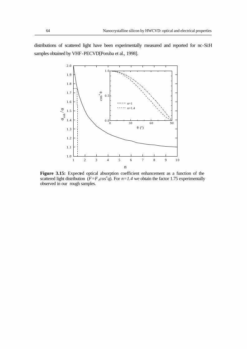
64 Nanocrystalline silicon by HWCVD: optical and electrical properties
distributions of scattered light have been experimentally measured and reported for nc-Si:H
samples obtained by VHF-PECVD[Poruba et al., 1998].
1 2 3 4 5 6 7 8 9 1 01.0
1.1
1.2
1.3
1.4
1.5
1.6
1.7
1.8
1.9
2.0
n
α enh /
α
0 30 60 900.0
0.5
1.0
n=1
n=1.4
cos n
θ
θ (º)
Figure 3.15: Expected optical absorption coefficient enhancement as a function of the scattered light distribution (Φ=Φocosnθ). For n=1.4 we obtain the factor 1.75 experimentally observed in our rough samples.
Thin film nanocrystalline silicon solar cells obtained by Hot-Wire CVD 65
3.2. Electrical properties 3.2.1. Dark conductivity of undoped nanocrystalline silicon
Though dark conductivity is possibly the most simple electrical characterisation of a
semiconductor, it allows to extract valuable information if the obtained data are accurately
analysed. The dark conductivity σ of any semiconductor can be calculated as
( )pne pn µµσ += (3.17)
where e is the elementary charge, n and p the electron and hole densities and µ n and µ p
their mobilities in the conduction and valence bands respectively. To take into account the
effect of the temperature we must consider that
−−=
Tk
EENn
B
FCC exp
−−=
Tk
EENp
B
VFV exp (3.18)
with EC and EV the energy levels of the conduction and valence band edges, EF the Fermi-
level, NC and NV the conduction and valence band effective densities of states respectively
and kB the Boltzmann’s constant. In an ideally intrinsic semiconductor, electrons in the
conduction band can be only those thermally activated from previously occupied states in
the valence band, i.e., n=p=ni where ni is the intrinsic carrier density given by
−==
Tk
ENNnpn
B
gVCi
2/exp (3.19)
Hence, the dark conductivity of an intrinsic semiconductor is
( )
−=
−+=
TkE
Tk
ENNe
B
ao
B
gVCpn exp
2/exp σµµσ (3.20)
where we have introduced the thermal activation energy Ea and prefactor σo of the dark
conductivity. In the same way, for n- and p-type semiconductors we obtain a similar
behaviour but with different expressions for Ea and σo
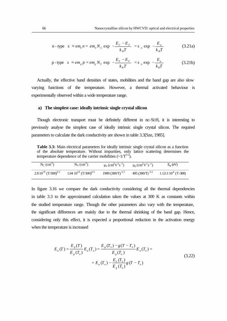
66 Nanocrystalline silicon by HWCVD: optical and electrical properties
−=
−−=≈
Tk
E
Tk
EENene
B
ao
B
FCCnn expexp type-n σµµσ (3.21a)
−=
−−=≈
Tk
E
Tk
EENepe
B
ao
B
VFVpp expexp type-p σµµσ (3.21b)
Actually, the effective band densities of states, mobilities and the band gap are also slow
varying functions of the temperature. However, a thermal activated behaviour is
experimentally observed within a wide temperature range.
a) The simplest case: ideally intrinsic single crystal silicon
Though electronic transport must be definitely different in nc-Si:H, it is interesting to
previously analyse the simplest case of ideally intrinsic single crystal silicon. The required
parameters to calculate the dark conductivity are shown in table 3.3[Sze, 1985].
Table 3.3: Main electrical parameters for ideally intrinsic single crystal silicon as a function of the absolute temperature. Without impurities, only lattice scattering determines the temperature dependence of the carrier mobilities (~1/T3/2).
NC (cm-3) NV (cm-3) µn (cm2V-1s -1) µp (cm2V-1s -1) Eg (eV)
2.8 1019 (T/300)3/2 1.04 1019 (T/300)3/2 1900 (300/T) 3/2 495 (300/T) 3/2 1.12-3 10-4 (T-300)
In figure 3.16 we compare the dark conductivity considering all the thermal dependencies
in table 3.3 to the approximated calculation taken the values at 300 K as constants within
the studied temperature range. Though the other parameters also vary with the temperature,
the significant differences are mainly due to the thermal shrinking of the band gap. Hence,
considering only this effect, it is expected a proportional reduction in the activation energy
when the temperature is increased
)()(
)()(
)()(
)()()(
)(
)()(
oog
oaoa
oaog
oogoa
og
ga
TTTETE
TE
TETE
TTTETE
TE
TETE
−−=
=−−
==
γ
γ
(3.22)
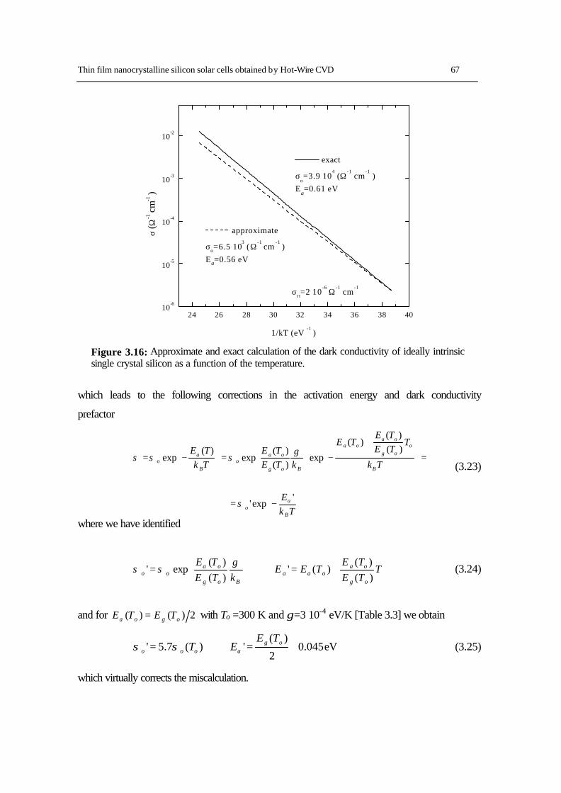
Thin film nanocrystalline silicon solar cells obtained by Hot-Wire CVD 67
24 26 28 30 32 34 36 38 4010
-6
10-5
10-4
10-3
10-2
σr t=2 10-6 Ω
-1 cm
-1
approximate
σo=6.5 103 (Ω
-1 cm
-1 )
Ea=0.56 eV
exact
σo=3.9 10
4 (Ω
-1 cm
-1 )
Ea=0.61 eV
1/kT (eV -1
)
σ (Ω
-1 c
m-1 )
Figure 3.16: Approximate and exact calculation of the dark conductivity of ideally intrinsic single crystal silicon as a function of the temperature.
which leads to the following corrections in the activation energy and dark conductivity
prefactor
−=
=
+
−
=
−=
TkE
Tk
TTETE
TE
kTETE
TkTE
B
ao
B
oog
oaoa
Bog
oao
B
ao
'exp'
)()(
)(
exp)()(
exp)(
exp
σ
γσσσ
(3.23)
where we have identified
TTETE
TEEkTE
TE
og
oaoaa
Bog
oaoo )(
)()('
)(
)(exp' +=
=
γσσ (3.24)
and for 2)()( ogoa TETE = with To =300 K and γ =3 10-4 eV/K [Table 3.3] we obtain
eV 045.02
)(' )(7.5' +== og
aooo
TEETσσ (3.25)
which virtually corrects the miscalculation.
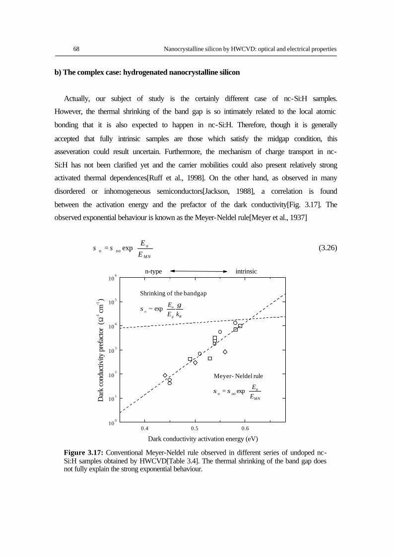
68 Nanocrystalline silicon by HWCVD: optical and electrical properties
b) The complex case: hydrogenated nanocrystalline silicon
Actually, our subject of study is the certainly different case of nc-Si:H samples.
However, the thermal shrinking of the band gap is so intimately related to the local atomic
bonding that it is also expected to happen in nc-Si:H. Therefore, though it is generally
accepted that fully intrinsic samples are those which satisfy the midgap condition, this
asseveration could result uncertain. Furthermore, the mechanism of charge transport in nc-
Si:H has not been clarified yet and the carrier mobilities could also present relatively strong
activated thermal dependences[Ruff et al., 1998]. On the other hand, as observed in many
disordered or inhomogeneous semiconductors[Jackson, 1988], a correlation is found
between the activation energy and the prefactor of the dark conductivity[Fig. 3.17]. The
observed exponential behaviour is known as the Meyer-Neldel rule[Meyer et al., 1937]
=
MN
aooo
E
Eexpσσ (3.26)
0.4 0.5 0.610
0
101
102
103
104
105
106
n-type intrinsic
Dark conductivity activation energy (eV)
Dar
k co
nduc
tivity
pre
fact
or (
Ω-1
cm-1
)
Figure 3.17: Conventional Meyer-Neldel rule observed in different series of undoped nc-Si:H samples obtained by HWCVD[Table 3.4]. The thermal shrinking of the band gap does not fully explain the strong exponential behaviour.
Bg
ao kE
E γσ exp~
bandgap theof Shrinking
=
MN
aooo E
Eexp
rule Neldel-Meyer
σσ
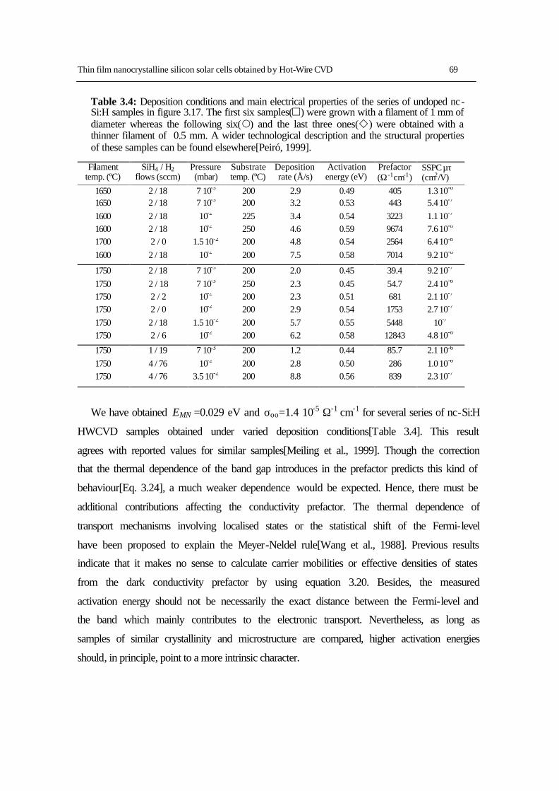
Thin film nanocrystalline silicon solar cells obtained by Hot-Wire CVD 69
Table 3.4: Deposition conditions and main electrical properties of the series of undoped nc-Si:H samples in figure 3.17. The first six samples(£) were grown with a filament of 1 mm of diameter whereas the following six() and the last three ones(¯) were obtained with a thinner filament of 0.5 mm. A wider technological description and the structural properties of these samples can be found elsewhere[Peiró, 1999].
Filament temp. (ºC)
SiH4 / H2 flows (sccm)
Pressure (mbar)
Substrate temp. (ºC)
Deposition rate (Å/s)
Activation energy (eV)
Prefactor (Ω -1cm-1)
SSPC µτ (cm2/V)
1650 2 / 18 7 10-3 200 2.9 0.49 405 1.3 10-6 1650 2 / 18 7 10-3 200 3.2 0.53 443 5.4 10-7
1600 2 / 18 10-2 225 3.4 0.54 3223 1.1 10-7 1600 2 / 18 10-2 250 4.6 0.59 9674 7.6 10-8 1700 2 / 0 1.5 10-2 200 4.8 0.54 2564 6.4 10-8
1600 2 / 18 10-2 200 7.5 0.58 7014 9.2 10-8
1750 2 / 18 7 10-3 200 2.0 0.45 39.4 9.2 10-7
1750 2 / 18 7 10-3 250 2.3 0.45 54.7 2.4 10-6 1750 2 / 2 10-2 200 2.3 0.51 681 2.1 10-7 1750 2 / 0 10-2 200 2.9 0.54 1753 2.7 10-7
1750 2 / 18 1.5 10-2 200 5.7 0.55 5448 10-7 1750 2 / 6 10-2 200 6.2 0.58 12843 4.8 10-8
1750 1 / 19 7 10-3 200 1.2 0.44 85.7 2.1 10-6
1750 4 / 76 10-2 200 2.8 0.50 286 1.0 10-6 1750 4 / 76 3.5 10-2 200 8.8 0.56 839 2.3 10-7
We have obtained EMN =0.029 eV and σoo=1.4 10-5 Ω-1 cm-1 for several series of nc-Si:H
HWCVD samples obtained under varied deposition conditions[Table 3.4]. This result
agrees with reported values for similar samples[Meiling et al., 1999]. Though the correction
that the thermal dependence of the band gap introduces in the prefactor predicts this kind of
behaviour[Eq. 3.24], a much weaker dependence would be expected. Hence, there must be
additional contributions affecting the conductivity prefactor. The thermal dependence of
transport mechanisms involving localised states or the statistical shift of the Fermi-level
have been proposed to explain the Meyer-Neldel rule[Wang et al., 1988]. Previous results
indicate that it makes no sense to calculate carrier mobilities or effective densities of states
from the dark conductivity prefactor by using equation 3.20. Besides, the measured
activation energy should not be necessarily the exact distance between the Fermi-level and
the band which mainly contributes to the electronic transport. Nevertheless, as long as
samples of similar crystallinity and microstructure are compared, higher activation energies
should, in principle, point to a more intrinsic character.
70 Nanocrystalline silicon by HWCVD: optical and electrical properties
3.2.2. Evidences of contaminants incorporation
A problem often encountered with as grown undoped nc-Si:H is its generally
pronounced n-type character. It has been suggested that either a large content of oxygen
impurities or native defects within the layers could be responsible for this unwanted Fermi-
level shift[Lucovsky et al., 1993]. The group at University of Neuchâtel showed that the n-
type behaviour of their VHF-PECVD layers was mainly linked to oxygen impurities acting
as unwanted donor levels in the gap[Torres et al., 1996]. Depending on the deposition
conditions, our undoped nc-Si:H samples obtained by HWCVD also present activation
energies far from the midgap condition[Voz et al., 2000]. Besides, the thermopower of
these samples evidences a certain as grown n-type character. In addition, several shallow
donor levels (EC-ED≤0.14eV) which could be attributed to oxygen were resolved by Deep
Level Transient Spectroscopy (DLTS) in our samples[Stöger et al., 1999]. Low p-type
doping levels (solid phase B/Si ratio ~10-4 ) lead to higher activation energies as well as
lower room temperature dark conductivities[Fig. 3.18]. This result could be explained by
the compensation of donor levels related to the incorporation of contaminants[Voz et al.,
2000]. Similar results have been reported for similar boron concentrations in HWCVD
samples[Wanka et al., 1995]. By contrast, in the case of nc-Si:H obtained by VHF-PECVD,
compensation was achieved at much lower concentrations (B/Si~10-6 )[Flückiger, 1995].
Actually, several studies point to a higher incorporation of contaminants in HWCVD nc-
Si:H samples when they are compared to VHF-PECVD material[Schubert et al., 1998].
Though the eventual incorporation of metallic components from the wire could explain this
result, a higher incorporation of residual gas phase contaminants (oxygen, carbon...) was
also detected. This difference was found even with the same ultra-high vacuum
specifications and feedgas purity. There are some differences between HWCVD and
PECVD related processes which could explain this result. Much more atomic hydrogen is
generated at the hot wire than in a glow discharge. Thus, chemical reduction of the highly
oxidised silicon on the walls of the chamber could increase the outgassing rate. This would
lead to a higher incorporation of contaminants. Actually, we have certainly observed a
clearly increased outgassing rate from the walls of the chamber after any HWCVD process.
Furthermore, we have observed that nc-Si:H samples by HWCVD oxidise much faster
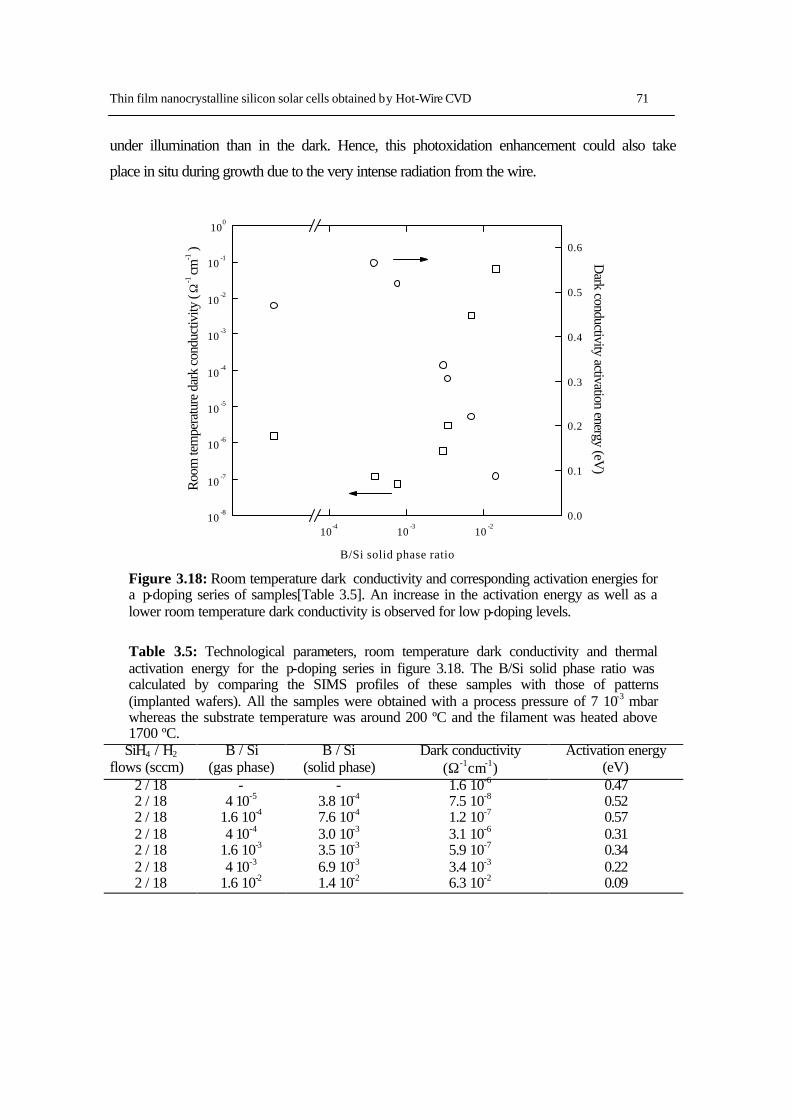
Thin film nanocrystalline silicon solar cells obtained by Hot-Wire CVD 71
under illumination than in the dark. Hence, this photoxidation enhancement could also take
place in situ during growth due to the very intense radiation from the wire.
Figure 3.18: Room temperature dark conductivity and corresponding activation energies for a p-doping series of samples[Table 3.5]. An increase in the activation energy as well as a lower room temperature dark conductivity is observed for low p-doping levels.
Table 3.5: Technological parameters, room temperature dark conductivity and thermal activation energy for the p-doping series in figure 3.18. The B/Si solid phase ratio was calculated by comparing the SIMS profiles of these samples with those of patterns (implanted wafers). All the samples were obtained with a process pressure of 7 10-3 mbar whereas the substrate temperature was around 200 ºC and the filament was heated above 1700 ºC.
SiH4 / H2 flows (sccm)
B / Si (gas phase)
B / Si (solid phase)
Dark conductivity (Ω-1cm-1)
Activation energy (eV)
2 / 18 - - 1.6 10-6 0.47 2 / 18 4 10-5 3.8 10-4 7.5 10-8 0.52 2 / 18 1.6 10-4 7.6 10-4 1.2 10-7 0.57 2 / 18 4 10-4 3.0 10-3 3.1 10-6 0.31 2 / 18 1.6 10-3 3.5 10-3 5.9 10-7 0.34 2 / 18 4 10-3 6.9 10-3 3.4 10-3 0.22 2 / 18 1.6 10-2 1.4 10-2 6.3 10-2 0.09
10-4
10-3
10-2
10-8
10-7
10-6
10-5
10-4
10-3
10-2
10-1
100
Dark conductivity activation energy (eV
)
B/Si solid phase ratio
Roo
m te
mpe
ratu
re d
ark
cond
uctiv
ity (
Ω-1
cm-1
)
0.0
0.1
0.2
0.3
0.4
0.5
0.6
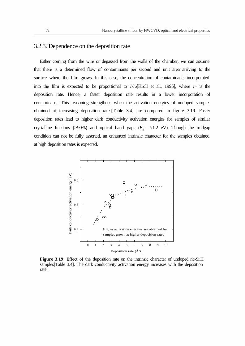
72 Nanocrystalline silicon by HWCVD: optical and electrical properties
3.2.3. Dependence on the deposition rate
Either coming from the wire or degassed from the walls of the chamber, we can assume
that there is a determined flow of contaminants per second and unit area arriving to the
surface where the film grows. In this case, the concentration of contaminants incorporated
into the film is expected to be proportional to 1/rd[Kroll et al., 1995], where rd is the
deposition rate. Hence, a faster deposition rate results in a lower incorporation of
contaminants. This reasoning strengthens when the activation energies of undoped samples
obtained at increasing deposition rates[Table 3.4] are compared in figure 3.19. Faster
deposition rates lead to higher dark conductivity activation energies for samples of similar
crystalline fractions (≥90%) and optical band gaps (Eg ≈1.2 eV). Though the midgap
condition can not be fully asserted, an enhanced intrinsic character for the samples obtained
at high deposition rates is expected.
0 1 2 3 4 5 6 7 8 9 10
0.4
0.5
0.6
Higher activation energies are obtained for
samples grown at higher deposition rates
Deposition rate (Å/s)
Dar
k co
nduc
tivity
act
ivat
ion
ener
gy (
eV)
Figure 3.19: Effect of the deposition rate on the intrinsic character of undoped nc-Si:H samples[Table 3.4]. The dark conductivity activation energy increases with the deposition rate.
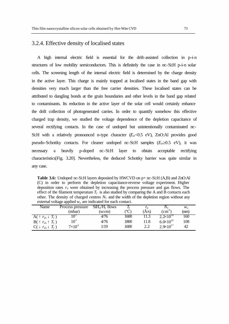
Thin film nanocrystalline silicon solar cells obtained by Hot-Wire CVD 73
3.2.4. Effective density of localised states
A high internal electric field is essential for the drift-assisted collection in p-i-n
structures of low mobility semiconductors. This is definitely the case in nc-Si:H p-i-n solar
cells. The screening length of the internal electric field is determined by the charge density
in the active layer. This charge is mainly trapped at localised states in the band gap with
densities very much larger than the free carrier densities. These localised states can be
attributed to dangling bonds at the grain boundaries and other levels in the band gap related
to contaminants. Its reduction in the active layer of the solar cell would certainly enhance
the drift collection of photogenerated carries. In order to quantify somehow this effective
charged trap density, we studied the voltage dependence of the depletion capacitance of
several rectifying contacts. In the case of undoped but unintentionally contaminated nc-
Si:H with a relatively pronounced n-type character (Ea<0.5 eV), ZnO:Al provides good
pseudo-Schottky contacts. For cleaner undoped nc-Si:H samples (Ea≥0.5 eV), it was
necessary a heavily p-doped nc-Si:H layer to obtain acceptable rectifying
characteristics[Fig. 3.20]. Nevertheless, the deduced Schottky barrier was quite similar in
any case.
Table 3.6: Undoped nc-Si:H layers deposited by HWCVD on p+ nc-Si:H (A,B) and ZnO:Al (C) in order to perform the depletion capacitance-reverse voltage experiment. Higher deposition rates rd were obtained by increasing the process pressure and gas flows. The effect of the filament temperature Tf is also studied by comparing the A and B contacts each other. The density of charged centres NC and the width of the depletion region without any external voltage applied wo are indicated for each contact.
Name Process pressure (mbar)
SiH4/H2 flows (sccm)
Tf (ºC)
rd (Å/s)
NC
(cm-3) wo
(nm) A( ↑ rd, ↓ Tf ) 10-1 4/76 1600 11.3 2.2×10¹⁶ 160 B( ↑ rd, ↑ Tf ) 10-1 4/76 1800 11.8 6.0×10¹⁶ 108 C( ↓ rd, ↓ Tf ) 7×10⁻³ 1/19 1600 2.2 2.9×10¹⁷ 42
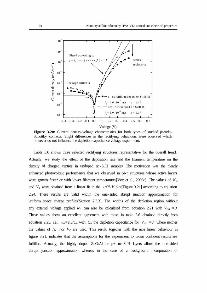
74 Nanocrystalline silicon by HWCVD: optical and electrical properties
-0.4 -0.3 -0.2 -0.1 0.0 0.1 0.2 0.3 0.4 0.5 0.6 0.7
10-5
10-4
10-3
10-2
10-1
100
101
102
Fitted according to
j = jo [ exp ( eV / nk BT ) - 1 ]
leakage currents
series
resistance
p+ nc-Si:H/undoped nc-Si:H (A)
jo = 4.6 ×10⁻⁴
mA n = 1.46
ZnO:Al/undoped nc-Si:H (C)
jo = 6.0 ×10⁻⁴
mA n = 1.17
Voltage (V)
Cur
rent
den
sity
(mA
/cm
2 )
Figure 3.20: Current density-voltage characteristics for both types of studied pseudo-Schottky contacts. Slight differences in the rectifying behaviours were observed which however do not influence the depletion capacitance-voltage experiment.
Table 3.6 shows three selected rectifying structures representative for the overall trend.
Actually, we study the effect of the deposition rate and the filament temperature on the
density of charged centres in undoped nc-Si:H samples. The motivation was the clearly
enhanced photovoltaic performance that we observed in p-i-n structures whose active layers
were grown faster or with lower filament temperatures[Voz et al., 2000c]. The values of NC
and Vd were obtained from a linear fit in the 1/C2-V plot[Figure 3.21] according to equation
2.24. These results are valid within the one-sided abrupt junction approximation for
uniform space charge profiles[Section 2.3.3]. The widths of the depletion region without
any external voltage applied wo can also be calculated from equation 2.21 with Vext =0.
These values show an excellent agreement with those in table 3.6 obtained directly from
equation 2.25, i.e., wo=εsS/Co with Co the depletion capacitance for Vext =0 where neither
the values of NC nor Vd are used. This result, together with the nice linear behaviour in
figure 3.21, indicates that the assumptions for the experiment to obtain confident results are
fulfilled. Actually, the highly doped ZnO:Al or p+ nc-Si:H layers allow the one-sided
abrupt junction approximation whereas in the case of a background incorporation of
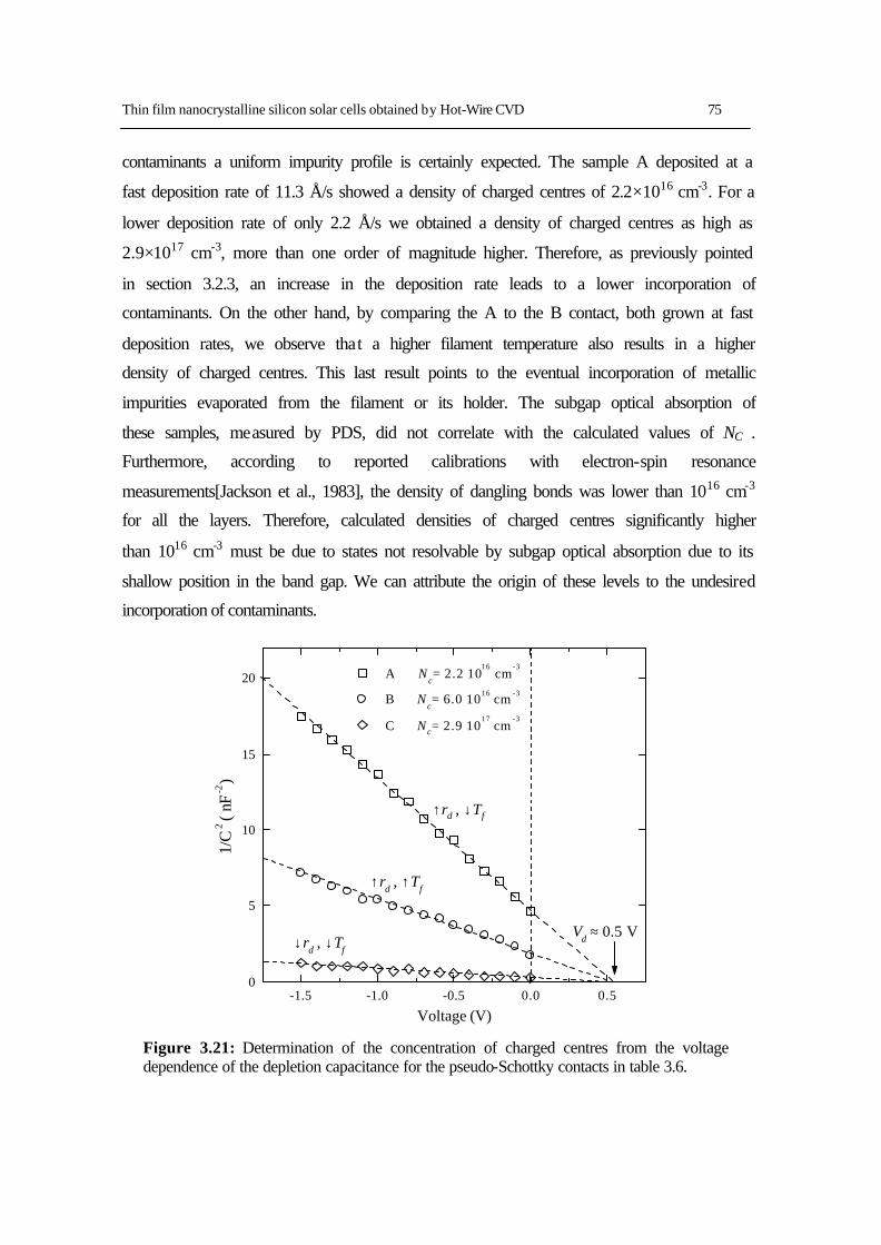
Thin film nanocrystalline silicon solar cells obtained by Hot-Wire CVD 75
contaminants a uniform impurity profile is certainly expected. The sample A deposited at a
fast deposition rate of 11.3 Å/s showed a density of charged centres of 2.2×1016 cm-3. For a
lower deposition rate of only 2.2 Å/s we obtained a density of charged centres as high as
2.9×1017 cm-3, more than one order of magnitude higher. Therefore, as previously pointed
in section 3.2.3, an increase in the deposition rate leads to a lower incorporation of
contaminants. On the other hand, by comparing the A to the B contact, both grown at fast
deposition rates, we observe that a higher filament temperature also results in a higher
density of charged centres. This last result points to the eventual incorporation of metallic
impurities evaporated from the filament or its holder. The subgap optical absorption of
these samples, measured by PDS, did not correlate with the calculated values of NC .
Furthermore, according to reported calibrations with electron-spin resonance
measurements[Jackson et al., 1983], the density of dangling bonds was lower than 1016 cm-3
for all the layers. Therefore, calculated densities of charged centres significantly higher
than 1016 cm-3 must be due to states not resolvable by subgap optical absorption due to its
shallow position in the band gap. We can attribute the origin of these levels to the undesired
incorporation of contaminants.
-1.5 -1.0 -0.5 0.0 0.50
5
10
15
20
↑rd , ↓Tf
↑rd , ↑Tf
↓rd , ↓Tf
Vd ≈ 0.5 V
A Nc= 2.2 10
16 cm
-3
B Nc= 6.0 10
16 cm
-3
C Nc= 2.9 1017
cm-3
Voltage (V)
1/C
2 ( nF
-2 )
Figure 3.21: Determination of the concentration of charged centres from the voltage dependence of the depletion capacitance for the pseudo-Schottky contacts in table 3.6.
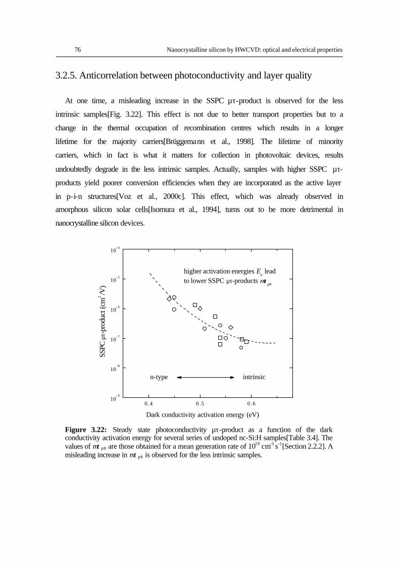
76 Nanocrystalline silicon by HWCVD: optical and electrical properties
3.2.5. Anticorrelation between photoconductivity and layer quality
At one time, a misleading increase in the SSPC µτ-product is observed for the less
intrinsic samples[Fig. 3.22]. This effect is not due to better transport properties but to a
change in the thermal occupation of recombination centres which results in a longer
lifetime for the majority carriers[Brüggemann et al., 1998]. The lifetime of minority
carriers, which in fact is what it matters for collection in photovoltaic devices, results
undoubtedly degrade in the less intrinsic samples. Actually, samples with higher SSPC µτ-
products yield poorer conversion efficiencies when they are incorporated as the active layer
in p-i-n structures[Voz et al., 2000c]. This effect, which was already observed in
amorphous silicon solar cells[Isomura et al., 1994], turns out to be more detrimental in
nanocrystalline silicon devices.
0.4 0.5 0.610
-9
10-8
10-7
10-6
10-5
10-4
n-type intrinsic
higher activation energies Ea lead
to lower SSPC µτ-products µτ ph
Dark conductivity activation energy (eV)
SSPC
µτ-
prod
uct (
cm2 /V
)
Figure 3.22: Steady state photoconductivity µτ-product as a function of the dark conductivity activation energy for several series of undoped nc-Si:H samples[Table 3.4]. The values of µτ ph are those obtained for a mean generation rate of 1019 cm-3 s-1[Section 2.2.2]. A misleading increase in µτ ph is observed for the less intrinsic samples.
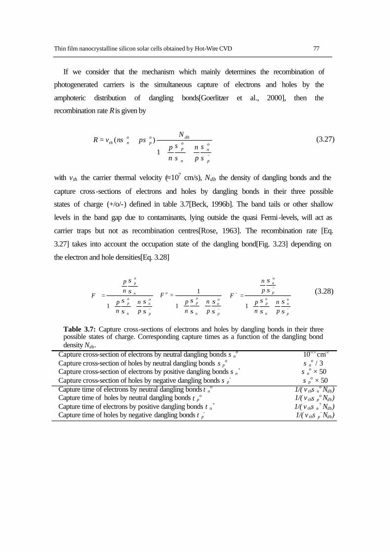
Thin film nanocrystalline silicon solar cells obtained by Hot-Wire CVD 77
If we consider that the mechanism which mainly determines the recombination of
photogenerated carriers is the simultaneous capture of electrons and holes by the
amphoteric distribution of dangling bonds[Goerlitzer et al., 2000], then the
recombination rate R is given by
−+ ++
+=
p
on
n
op
dbop
onth
pn
np
NpnvR
σσ
σ
σσσ
1
)( (3.27)
with vth the carrier thermal velocity (≈107 cm/s), Ndb the density of dangling bonds and the
capture cross-sections of electrons and holes by dangling bonds in their three possible
states of charge (+/o/-) defined in table 3.7[Beck, 1996b]. The band tails or other shallow
levels in the band gap due to contaminants, lying outside the quasi Fermi-levels, will act as
carrier traps but not as recombination centres[Rose, 1963]. The recombination rate [Eq.
3.27] takes into account the occupation state of the dangling bond[Fig. 3.23] depending on
the electron and hole densities[Eq. 3.28]
−+
++
++
=
p
on
n
op
n
op
pn
np
np
F
σσ
σ
σσ
σ
1
−+ ++
=
p
on
n
op
o
pn
np
F
σσ
σ
σ1
1
−+
−−
++
=
p
on
n
op
p
on
pn
np
pn
F
σσ
σ
σ
σσ
1
(3.28)
Table 3.7: Capture cross-sections of electrons and holes by dangling bonds in their three possible states of charge. Corresponding capture times as a function of the dangling bond density Ndb.
Capture cross-section of electrons by neutral dangling bonds σ no 10-15 cm-2
Capture cross-section of holes by neutral dangling bonds σ po σ n
o / 3 Capture cross-section of electrons by positive dangling bonds σ n
+ σ no × 50
Capture cross-section of holes by negative dangling bonds σ p- σ p
o × 50 Capture time of electrons by neutral dangling bonds τ n
o 1/( v thσ no Ndb)
Capture time of holes by neutral dangling bonds τ po 1/( v thσ p
o Ndb) Capture time of electrons by positive dangling bonds τ n
+ 1/( v thσ n+ Ndb)
Capture time of holes by negative dangling bonds τ p- 1/( v thσ p
- Ndb)
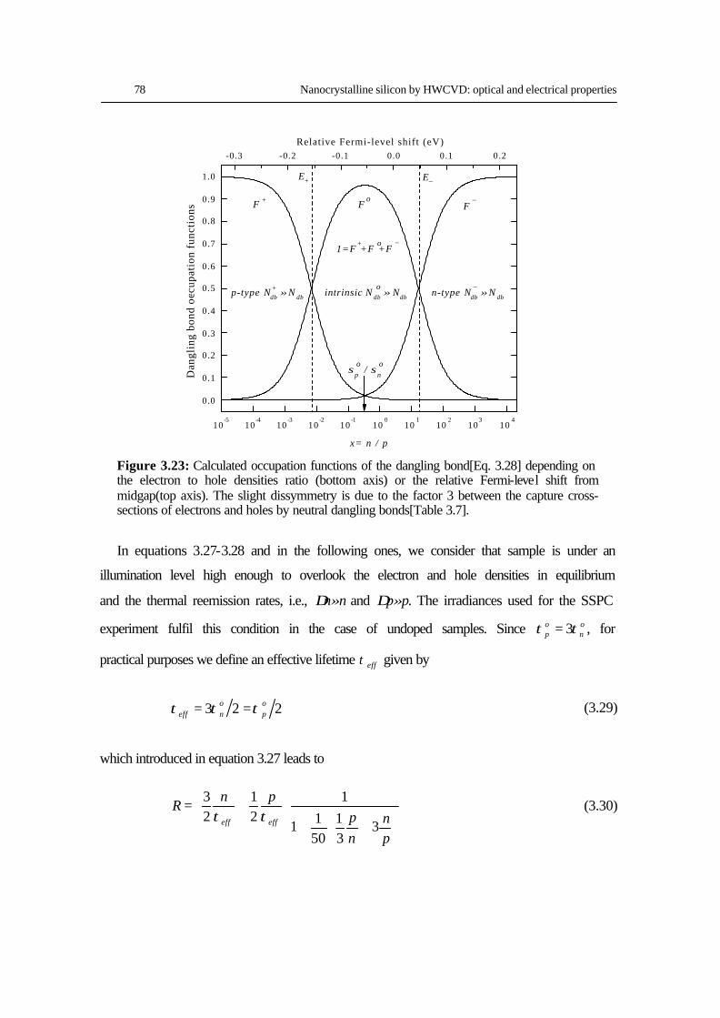
78 Nanocrystalline silicon by HWCVD: optical and electrical properties
10-5
10-4
10-3
10-2
10-1
100
101
102
103
104
0.0
0.1
0.2
0.3
0.4
0.5
0.6
0.7
0.8
0.9
1.0 _E+E
Relative Fermi-level shift (eV)
_o+1=F +F +F
ointrinsic N db ≈ Ndb
_n-type Ndb ≈ N db
+p-type Ndb ≈ N db+
x= n / p
Dan
glin
g bo
nd o
ccup
atio
n fu
ncti
ons
+F
ooσ
p / σ
n
_F
oF
-0.3 -0.2 -0.1 0.0 0.1 0.2
Figure 3.23: Calculated occupation functions of the dangling bond[Eq. 3.28] depending on the electron to hole densities ratio (bottom axis) or the relative Fermi-level shift from midgap(top axis). The slight dissymmetry is due to the factor 3 between the capture cross-sections of electrons and holes by neutral dangling bonds[Table 3.7].
In equations 3.27-3.28 and in the following ones, we consider that sample is under an
illumination level high enough to overlook the electron and hole densities in equilibrium
and the thermal reemission rates, i.e., ∆n≈n and ∆p≈p. The irradiances used for the SSPC
experiment fulfil this condition in the case of undoped samples. Since on
op ττ 3= , for
practical purposes we define an effective lifetime effτ given by
223 op
oneff τττ == (3.29)
which introduced in equation 3.27 leads to
++
+=
pn
np
pnR
effeff 331
5011
121
23
ττ (3.30)
Thin film nanocrystalline silicon solar cells obtained by Hot-Wire CVD 79
Since recombination equals the generation rate in steady state conditions, the lifetimes of
electrons and holes can be calculated from R = G = n /τ n = p /τ p arriving at
++
+= x
xxx
effn 331
501
113
2ττ (3.31a)
++
+= x
xxeffp 331
501
113
2ττ (3.31b)
where x=n/p is the ratio of the electron to hole densities. Depending on the character of the
samples, equation 3.31 can be further simplified.
a) n-type samples, x>>1
−==≈ p
opeff
n xxx τττ
τ5050
2 −==≈ p
opeff
p τττ
τ5050
2 (3.32a)
−≈
p
pR
τ (3.32b)
b) p-type samples, x<<1
+==≈ n
oneff
n τττ
τ5050
3/2
xxxn
oneff
p
+
==≈τττ
τ5050
3/2 (3.33a)
+≈n
nR
τ (3.33b)
c) midgap samples, x≈1
2eff
pn
τττ ≈≈ (3.34a)
op
on
pnR
ττ+≈ (3.34b)
As expected, in n-type and p-type samples the recombination rate is determined by the
very much shorter capture time of the minority carrier by the charged dangling bonds. In
the case of midgap samples, the recombination rate is simultaneously given by the capture
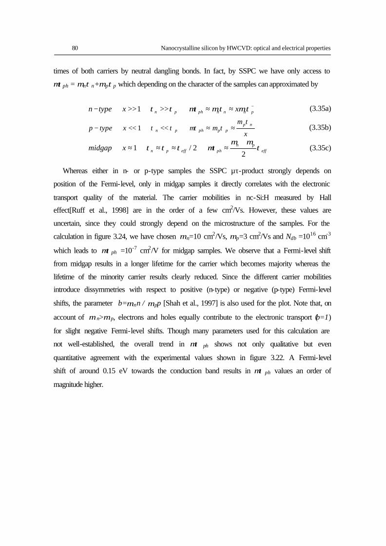
80 Nanocrystalline silicon by HWCVD: optical and electrical properties
times of both carriers by neutral dangling bonds. In fact, by SSPC we have only access to
µτ ph = µ nτ n+µ pτ p which depending on the character of the samples can approximated by
−≈≈⇒>>⇒>>⇒− pnnnphpn xxtypen τµτµµτττ1 (3.35a)
xxtypep
npppphpn
+
≈≈⇒<<⇒<<⇒−τµ
τµµτττ1 (3.35b)
effpn
pheffpnxmidgap τµµ
µττττ2
2/1+
≈⇒≈≈⇒≈⇒ (3.35c)
Whereas either in n- or p-type samples the SSPC µτ-product strongly depends on
position of the Fermi-level, only in midgap samples it directly correlates with the electronic
transport quality of the material. The carrier mobilities in nc-Si:H measured by Hall
effect[Ruff et al., 1998] are in the order of a few cm2/Vs. However, these values are
uncertain, since they could strongly depend on the microstructure of the samples. For the
calculation in figure 3.24, we have chosen µ n=10 cm2/Vs, µ p=3 cm2/Vs and Ndb =1016 cm-3
which leads to µτ ph =10-7 cm2/V for midgap samples. We observe that a Fermi-level shift
from midgap results in a longer lifetime for the carrier which becomes majority whereas the
lifetime of the minority carrier results clearly reduced. Since the different carrier mobilities
introduce dissymmetries with respect to positive (n-type) or negative (p-type) Fermi-level
shifts, the parameter b=µ nn / µ pp [Shah et al., 1997] is also used for the plot. Note that, on
account of µ n>µ p, electrons and holes equally contribute to the electronic transport (b=1)
for slight negative Fermi-level shifts. Though many parameters used for this calculation are
not well-established, the overall trend in µτ ph shows not only qualitative but even
quantitative agreement with the experimental values shown in figure 3.22. A Fermi-level
shift of around 0.15 eV towards the conduction band results in µτ ph values an order of
magnitude higher.
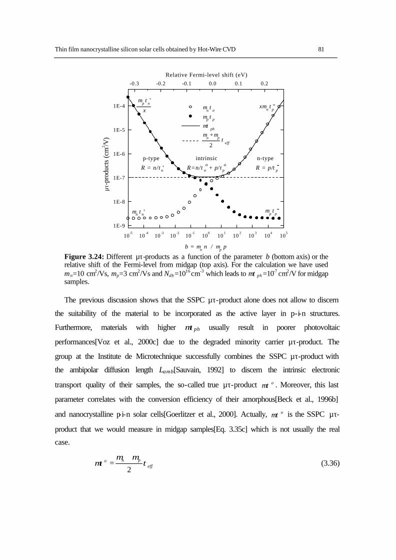
Thin film nanocrystalline silicon solar cells obtained by Hot-Wire CVD 81
10-5
10-4
10-3
10-2
10-1
100
101
102
103
104
105
1E-9
1E-8
1E-7
1E-6
1E-5
1E-4
oo -+
x
+µp τ
n -xµn τ
p
p-type intrinsic n-type
R = n/τn R=n/τn + p/τp R = p/τp
Relative Fermi-level shift (eV)
b = µn
n / µp
p
µτ-p
rodu
cts
(cm
2 /V)
µn τ
n
µp τp
µτ ph
τ eff2
µn +µ
p
+µn τn-µ
p τ
p
-0.3 -0.2 -0.1 0.0 0.1 0.2
Figure 3.24: Different µτ-products as a function of the parameter b (bottom axis) or the relative shift of the Fermi-level from midgap (top axis). For the calculation we have used µ n=10 cm2/Vs, µ p=3 cm2/Vs and Ndb =1016 cm-3 which leads to µτ ph =10-7 cm2/V for midgap samples.
The previous discussion shows that the SSPC µτ-product alone does not allow to discern
the suitability of the material to be incorporated as the active layer in p-i-n structures.
Furthermore, materials with higher µτ ph usually result in poorer photovoltaic
performances[Voz et al., 2000c] due to the degraded minority carrier µτ-product. The
group at the Institute de Microtechnique successfully combines the SSPC µτ-product with
the ambipolar diffusion length Lamb[Sauvain, 1992] to discern the intrinsic electronic
transport quality of their samples, the so-called true µτ-product oµτ . Moreover, this last
parameter correlates with the conversion efficiency of their amorphous[Beck et al., 1996b]
and nanocrystalline p-i-n solar cells[Goerlitzer et al., 2000]. Actually, oµτ is the SSPC µτ-
product that we would measure in midgap samples[Eq. 3.35c] which is not usually the real
case.
effpno τ
µµµτ
2
+= (3.36)
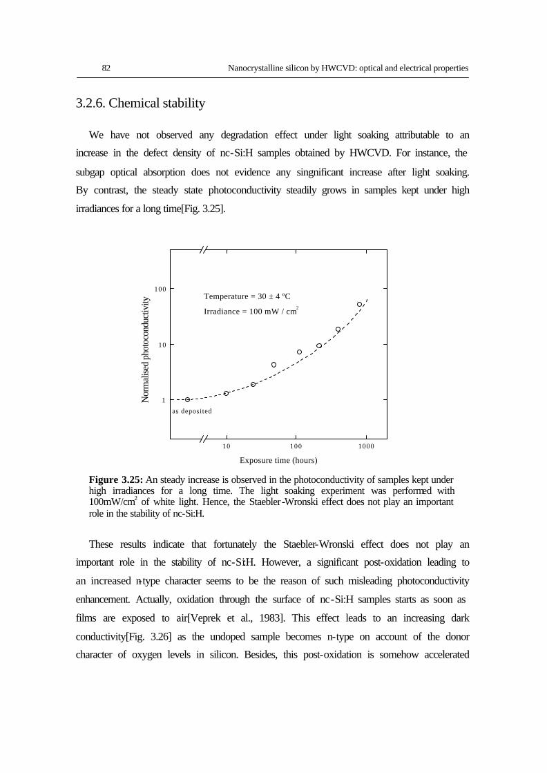
82 Nanocrystalline silicon by HWCVD: optical and electrical properties
3.2.6. Chemical stability
We have not observed any degradation effect under light soaking attributable to an
increase in the defect density of nc-Si:H samples obtained by HWCVD. For instance, the
subgap optical absorption does not evidence any singnificant increase after light soaking.
By contrast, the steady state photoconductivity steadily grows in samples kept under high
irradiances for a long time[Fig. 3.25].
10 100 1000
1
10
100
as deposited
Temperature = 30 ± 4 ºC
Irradiance = 100 mW / cm2
Exposure time (hours)
Nor
mal
ised
pho
toco
nduc
tivity
Figure 3.25: An steady increase is observed in the photoconductivity of samples kept under high irradiances for a long time. The light soaking experiment was performed with 100mW/cm2 of white light. Hence, the Staebler-Wronski effect does not play an important role in the stability of nc-Si:H.
These results indicate that fortunately the Staebler-Wronski effect does not play an
important role in the stability of nc-Si:H. However, a significant post-oxidation leading to
an increased n-type character seems to be the reason of such misleading photoconductivity
enhancement. Actually, oxidation through the surface of nc-Si:H samples starts as soon as
films are exposed to air[Veprek et al., 1983]. This effect leads to an increasing dark
conductivity[Fig. 3.26] as the undoped sample becomes n-type on account of the donor
character of oxygen levels in silicon. Besides, this post-oxidation is somehow accelerated
Thin film nanocrystalline silicon solar cells obtained by Hot-Wire CVD 83
under high irradiances when photons are able to break weak bonds thus favouring
oxidation[Fig. 3.27]. This relative chemical instability is a general feature of most (if not
all) nc-Si:H samples independently of the deposition technique[Goerlitzer et al., 1998].
26 28 30 32 34 36 38 4010
-7
10-6
10-5
10-4
10-3
10-2
10-1
after 45 days
σo = 40 Ω-1 cm
-1
Ea = 0.33 eV
as deposited
σo = 4×10³ Ω-1
cm-1
Ea = 0.58 eV
σ = σo exp (-Ea / kBT)
1 / kBT (eV
-1 )
Dar
k co
nduc
tivity
(Ω
-1 cm
-1 )
Figure 3.26: Change in the dark conductivity and activation energy of a nc-Si:H sample obtained by HWCVD due to post-oxidation in air. A pronounced n-type character is observed after 45 days.
We will show in the next chapter that the intrinsic character of the undoped active layer
in p-i-n structures is fundamental for successful photovoltaic conversion. Hence, the fearful
question which arises after evidencing this chemical instability is whether it bears the risk
of complete deterioration of nc-Si:H solar cells. Actually, this post-oxidation effect which
causes a serious problem for the characterisation of layers, could not be so dramatic in
devices where the active layer is sealed off by the doped and contact layers. Long-term
stable nc-Si:H p-i-n solar cells have been reported by VHF-PECVD[Meier et al., 1998b].
These devices incorporated a TCO/Ag back contact that could act as a capping layer apart
from enhancing light trapping.
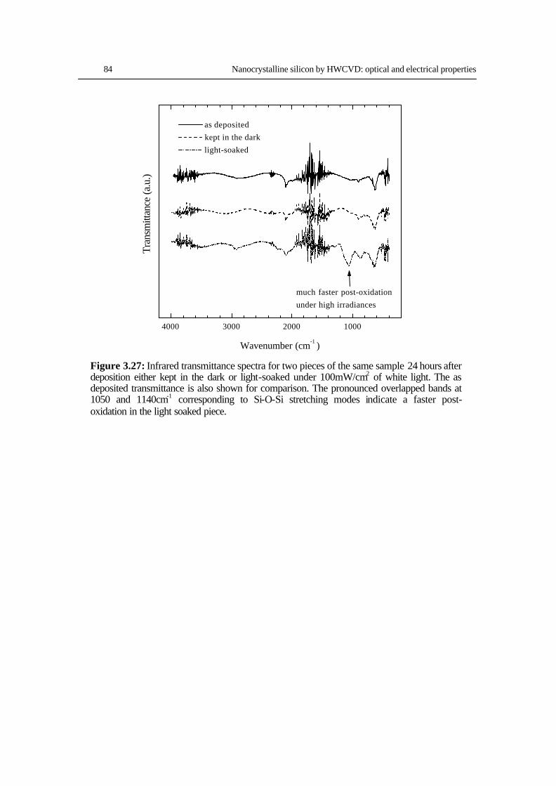
84 Nanocrystalline silicon by HWCVD: optical and electrical properties
4000 3000 2000 1000
much faster post-oxidation
under high irradiances
Wavenumber (cm-1 )
Tra
nsm
ittan
ce (a
.u.)
as deposited
kept in the dark
light-soaked
Figure 3.27: Infrared transmittance spectra for two pieces of the same sample 24 hours after deposition either kept in the dark or light-soaked under 100mW/cm2 of white light. The as deposited transmittance is also shown for comparison. The pronounced overlapped bands at 1050 and 1140cm-1 corresponding to Si-O-Si stretching modes indicate a faster post-oxidation in the light soaked piece.
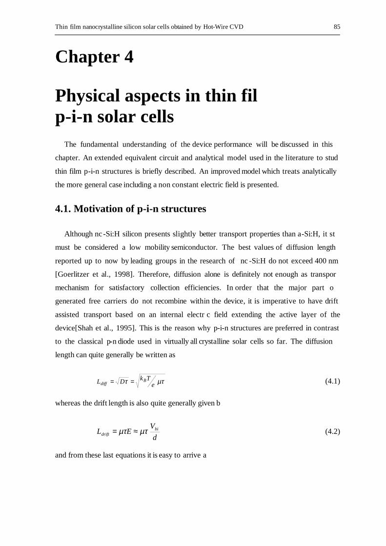
Thin film nanocrystalline silicon solar cells obtained by Hot-Wire CVD 85
Chapter 4 Physical aspects in thin fil p-i-n solar cells
The fundamental understanding of the device performance will be discussed in this
chapter. An extended equivalent circuit and analytical model used in the literature to stud
thin film p-i-n structures is briefly described. An improved model which treats analytically
the more general case including a non constant electric field is presented.
4.1. Motivation of p-i-n structures
Although nc -Si:H silicon presents slightly better transport properties than a-Si:H, it st
must be considered a low mobility semiconductor. The best values of diffusion length
reported up to now by leading groups in the research of nc -Si:H do not exceed 400 nm
[Goerlitzer et al., 1998]. Therefore, diffusion alone is definitely not enough as transpor
mechanism for satisfactory collection efficiencies. In order that the major part o
generated free carriers do not recombine within the device, it is imperative to have drift
assisted transport based on an internal electr c field extending the active layer of the
device[Shah et al., 1995]. This is the reason why p-i-n structures are preferred in contrast
to the classical p-n diode used in virtually all crystalline solar cells so far. The diffusion
length can quite generally be written as
µττ eTkDL B
diff == (4.1)
whereas the drift length is also quite generally given b
d
VEL bi
drift µτµτ ≈= (4.2)
and from these last equations it is easy to arrive a
86 Physical aspects in thin film p-i-n solar cells
d
L
d
L
eTk
V
L
L diffdiff
B
bi
diff
drift40≈
= (4.3)
This expression means that, for example, if the diffusion length is only a half of the
active layer thickness, the drift length would be ten times greater than it. Thus, a materia
whose properties hardly allow collection by diffusion can perfectly be suitable for drift
assisted devices. Actually, the internal electric field is partially screened by trapped charge
in the active layer. Hence, in order to enhance the photovoltaic conversion, it is essential to
minimise the density of dangling bonds and the incorporation of contaminants in the active
layer.
4.2. Equivalent circuit for low mobility thin film solar cells
4.2.1. The recombination term
Equivalent circuits are often used to describe the electrical behaviour of electronic
devices[Sze, 1985]. A simplistic view of a solar cell would be a diode plus a current source
connected in parallel which represents the photogenerated current. A parasitic parallel
resistance should also be included to correctly describe the device, especially in thin film
structures where shunting paths are easily formed. An additional series resistance takes
into account the voltage drop in the electrodes and the contact resistance. In most thin film
solar cells the series resistance is mainly determined by the sheet resistance of the TCO.
Generally speaking, recombination is relatively intense within low mobility a -Si:H and nc-
Si:H p-i-n solar cells because of the relatively high density of recombination centres
(dangling bonds) in the active layer. It is therefore intuitively reasonable to de scribe low
mobility -i-n silicon solar cells by introducing an additional recombination loss term jrec
into the equivalent circuit[Merten, 1996], a term which is symbolised by the curren
density sink (dashed lines) in figure 4.1.
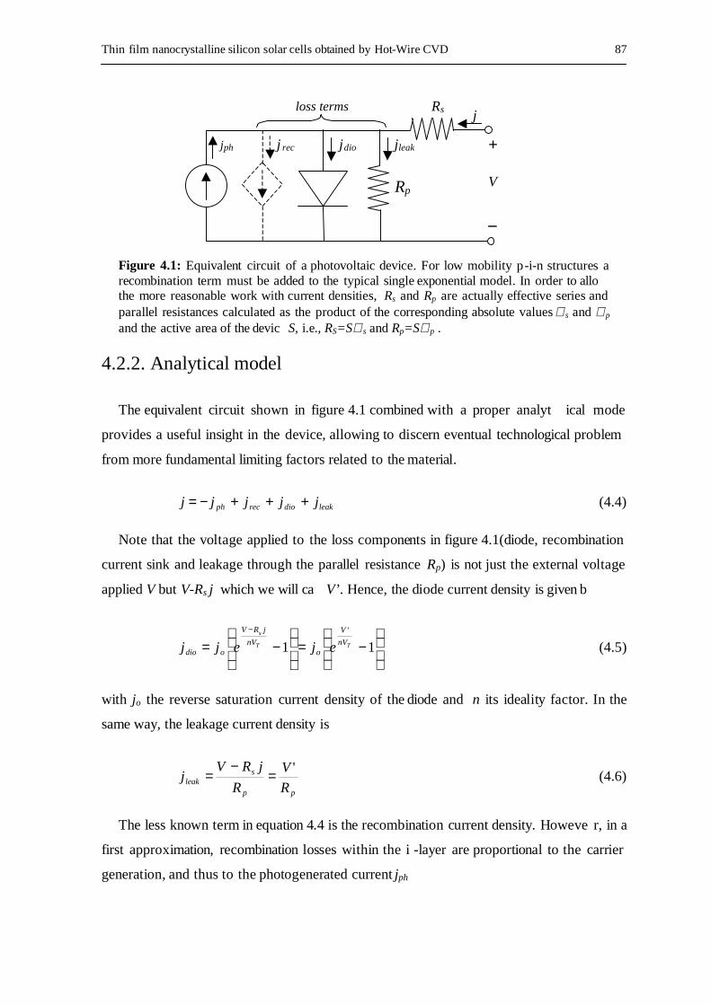
Thin film nanocrystalline silicon solar cells obtained by Hot-Wire CVD 87
Figure 4.1: Equivalent circuit of a photovoltaic device. For low mobility p-i-n structures a recombination term must be added to the typical single exponential model. In order to allothe more reasonable work with current densities, Rs and Rp are actually effective series and parallel resistances calculated as the product of the corresponding absolute values ℜ s and ℜ p and the active area of the devic S, i.e., RS=Sℜ s and Rp=Sℜ p .
4.2.2. Analytical model
The equivalent circuit shown in figure 4.1 combined with a proper analyt ical mode
provides a useful insight in the device, allowing to discern eventual technological problem
from more fundamental limiting factors related to the material.
leakdiorecph jjjjj +++−= (4.4)
Note that the voltage applied to the loss components in figure 4.1(diode, recombination
current sink and leakage through the parallel resistance Rp) is not just the external voltage
applied V but V-Rs j which we will ca V’. Hence, the diode current density is given b
11'
−=
−=
−
TT
s
nV
V
onV
jRV
odio ejejj (4.5)
with jo the reverse saturation current density of the diode and n its ideality factor. In the
same way, the leakage current density is
'
pp
sleak
R
V
R
jRVj =
−= (4.6)
The less known term in equation 4.4 is the recombination current density. Howeve r, in a
first approximation, recombination losses within the i -layer are proportional to the carrier
generation, and thus to the photogenerated current jph
jph j rec jdio jleak + V _
j loss terms Rs
Rp
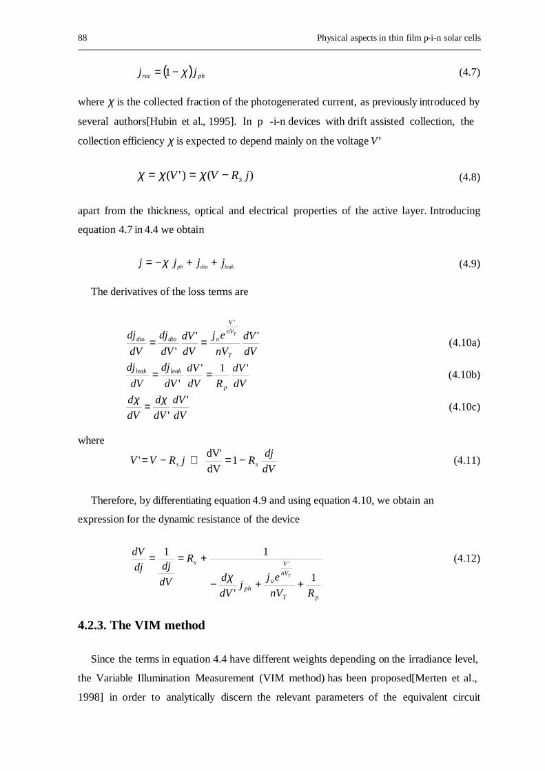
88 Physical aspects in thin film p-i-n solar cells
( ) phrec jj χ−= 1 (4.7)
where χ is the collected fraction of the photogenerated current, as previously introduced by
several authors[Hubin et al., 1995]. In p -i-n devices with drift assisted collection, the
collection efficiency χ is expected to depend mainly on the voltage V’
)()'( jRVV S−== χχχ (4.8)
apart from the thickness, optical and electrical properties of the active layer. Introducing
equation 4.7 in 4.4 we obtain
leakdioph jjjj ++−= χ (4.9)
The derivatives of the loss terms are
dV
dV
nV
ej
dV
dV
dV
dj
dV
dj
T
nV
V
odiodioT ''
'
'
== (4.10a)
dV
dV
RdV
dV
dV
dj
dV
dj
p
leakleak '1'
' == (4.10b)
dV
dV
dV
d
dV
d '
'
χχ = (4.10c)
where
dV
djRjRVV ss −=⇒−= 1
dV
dV' ' (4.11)
Therefore, by differentiating equation 4.9 and using equation 4.10, we obtain an
expression for the dynamic resistance of the device
pT
nV
V
oph
s
RnV
ejj
dV
d
R
dV
djdj
dV
T 1
'
11'
++−
+==
χ
(4.12)
4.2.3. The VIM method
Since the terms in equation 4.4 have different weights depending on the irradiance level,
the Variable Illumination Measurement (VIM method) has been proposed[Merten et al.,
1998] in order to analytically discern the relevant parameters of the equivalent circuit
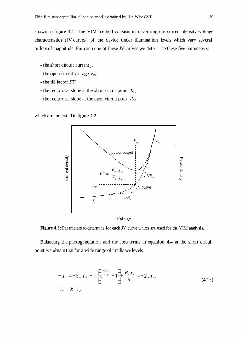
Thin film nanocrystalline silicon solar cells obtained by Hot-Wire CVD 89
shown in figure 4.1. The VIM method consists in measuring the current density -voltage
characteristics (JV curves) of the device under illumination levels which vary several
orders of magnitude. For each one of these JV curves we deter ne these five parameters:
- the short circuit current jsc
- the open circuit voltage Voc
- the fill factor FF
- the reciprocal slope at the short circuit poin Rsc
- the reciprocal slope at the open circuit poin Roc
which are indicated in figure 4.2.
Power density
power output
JV curve
Vmp
jmp
Voc
jsc
1/Roc
1/Rsc
Voltage
Cur
rent
den
sity
FF =V
oc j
sc
Vmp
jmp
Figure 4.2: Parameters to determine for each JV curve which are used for the VIM analysis.
Balancing the photogeneration and the loss terms in equation 4.4 at the short circui
point we obtain that for a wide range of irradiance levels
phscsc
phsc
p
scsnV
jR
ophscsc
jj
jR
jRejjj T
scs
χ
χχ
=
−≈+
−+−=−
1 (4.13)
90 Physical aspects in thin film p-i-n solar cells
whereas at the open circuit poin
=
=⇒=
+−≈+
−+−=
o
sc
sc
ocT
o
ph
ocTocnV
V
ophoc
nV
V
ophoc
p
ocnV
V
ophoc
j
jnV
j
jnVVejj
ejjR
Vejj
T
oc
T
oc
T
oc
χχ
χχ
χχ
lnln
10
(4.14)
which is basically the well known logarithmic dependence of the open circuit voltage as a
function of the short circuit current density[Möller,1993], but corrected wit h the ratio o
the collection efficiencies at the open and short circuit points. Within the model, according
to equation 4.12, the short circuit dynamic resistance is given by
pT
nV
IR
oph
sc
s
sc
sc
scsscss
RnV
ejj
dV
d
Rdj
dVR
jRjRVjRVV
T
scs
1
'
1
0'circuit short in '
++−
+=
=
−=−=⇒−=
−
χ (4.15)
This expression can be simplified depending on the irradiance:
a) for darkness and low illumination levels ( jph ≈ 0 and jsc ≈ 0 )
po
T
pT
osc R
j
nV
RnV
jR ||
11 =+
≈ (4.16)
b) whereas for medium and high illumination levels
sc
scscscC
sc
C
sc
sc
sc
ph
sc
sc
dV
djRV
j
V
j
dV
dj
dV
dR
−
==
=−
=−
≈
'
'
1
'
1
χχ
χχχ
(4.17)
where we have defined the collection volta ge VC as previously introduced by other
authors[Hof, 1999], a parameter intimately related to the collection mechanisms in the
active layer of the device.
Thin film nanocrystalline silicon solar cells obtained by Hot-Wire CVD 91
0 1 2 3 4 5-15
-10
-5
0
j = jsc
- V / Rsc
Voltage (V)
Cur
rent
den
sity
(mA
/cm
2 )
VC = R
sc × j
sc
Figure 4.3: Determination of the voltage collection from linear fits to the JV curves around the short circuit point.
c) and finally, for very high illumination it is only the series resistance which determines
the short circuit slope of the JV curve, i.e., ssc RR ≈
On the other hand, the open circuit dynamic resistance is
pT
nV
V
oph
oc
s
oc
oc
ocs
RnV
ejj
dV
d
Rdj
dVR
VVjRVV
T
oc
1
'
1
'circuit open in '
++−
+=
=
=⇒−=
χ (4.18)
which again takes simplified forms depending on the irradiance:
a) for darkness and very low illumination levels ( jph ≈ 0 and Voc ≈ 0 )
po
T
pT
ooc R
j
nV
RnV
jR ||
11 =+
≈ (4.19)
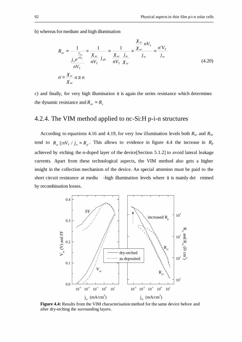
92 Physical aspects in thin film p-i-n solar cells
b) whereas for medium and high illumination
nnn
j
Vn
j
nV
j
nVj
nVnV
ej
R
oc
sc
sc
T
sc
Toc
sc
sc
sc
T
ocph
T
oc
T
nV
V
o
oc
T
oc
≥=
====≈
χχ
χχ
χχχ
'
'111
(4.20)
c) and finally, for very high illumination it is again the series resistance which determines
the dynamic resistance and soc RR ≈
4.2.4. The VIM method applied to nc-Si:H p-i-n structures
According to equations 4.16 and 4.19, for very low illumination levels both Rsc and Roc
tend to poTp RjnVR ≈/ || . This allows to evidence in figure 4.4 the increase in Rp
achieved by etching the n-doped layer of the device[Section 5.1.2] to avoid lateral leakage
currents. Apart from these technological aspects, the VIM method also gets a higher
insight in the collection mechanism of the device. An special attention must be paid to the
short circuit resistance at mediu -high illumination levels where it is mainly det rmined
by recombination losses.
10-3
10-2
10-1
100
101
0.0
0.1
0.2
0.3
0.4
Rsc
Roc
Voc
FF
jsc (mA/cm2)
Voc
(V
) and
FF
10-3
10-2
10-1
100
101
101
102
103
104
dry-etched as deposited
increased Rp
Rsc and R
oc ( Ω cm
2)
jsc (mA/cm2)
Figure 4.4: Results from the VIM characterisation method for the same device before and after dry-etching the surrounding layers.
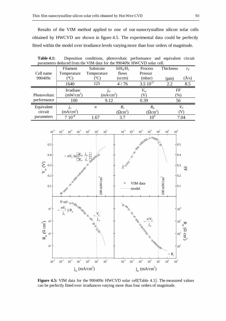
Thin film nanocrystalline silicon solar cells obtained by Hot-Wire CVD 93
Results of the VIM method applied to one of our nanocrystalline silicon solar cells
obtained by HWCVD are shown in figure 4.5. The experimental data could be perfectly
fitted within the model over irradiance levels varying more than four orders of magnitude.
Table 4.1: Deposition conditions, photovoltaic performance and equivalent circuit parameters deduced from the VIM data for the 990409c HWCVD solar cell.
Filament Temperature
(ºC)
Substrate Temperature
(ºC)
SiH4/H2 flows
(sccm)
Process Pressur (mbar)
Thickness
(µm)
rd
(Å/s)
Cell name 990409c
1640 125 4 / 76 3.5 10-2 2.2 8.5
Irradianc(mW/cm2)
jsc (mA/cm2)
Voc (V)
FF (%)
Photovoltaic performance 100 9.12 0.39 56
1
jo (mA/cm2)
n Rs (Ωcm2)
Rp (Ωcm2)
VC (V)
Equivalent circuit
parameters 7 10-4 1.67 3.7 105 7.04
Figure 4.5: VIM data for the 990409c HWCVD solar cell[Table 4.1]. The measured values can be perfectly fitted over irradiances varying more than four orders of magnitude.
0.1
0.2
0.3
0.4
0.5
10-4
10-3
10-2
10-1
100
101
102
100
mW
/cm
2
100
mW
/cm
2
Voc
(V
)
10-4
10-3
10-2
10-1
100
101
102
101
102
103
104
Rsc (Ω
cm
2 )
jsc (mA/cm2)
10-3
10-2
10-1
100
101
102
103
0.1
0.2
0.3
0.4
0.5
VIM data model
FF
10-3
10-2
10-1
100
101
102
103
101
102
103
104
jsc (mA/cm2)
Roc ( Ω
cm2)
o
sc
sc
ocT j
jnV
χχ
ln~
po
T Rj
nV||~
sc
C
j
V~
sc
T
j
Vn'~
sR~
94 Physical aspects in thin film p-i-n solar cells
According to equation 4.17, the short circuit resistance is inversely pr oportional to the
short circut current density for high enough illumination levels. In that case, the
recombination current density is the dominant loss term at the short circuit point whereas
the diode and leakage currents densities can be overlooked. In this situation, the short
circuit resistance arises as a parameter of capital interest in order to evaluate the electronic
quality of the active layer. Besides, in short circuit the electric field profile within the
active layer is not alterated by any external voltage. At this stage we can only say that the
better the collection mechanism throughout the active layer is, the greater the collection
voltage Vc will be in equation 4.17. In order to analytically relate the collection voltage
with the electronic properties of the device, it is necessary to obtain, at least near the shor
circuit point, a proper expression for the collection efficiency χ. But this is not an easy
subject at all.
4.3. Collection in p-i-n solar cells
4.3.1. The complexity of the problem
The collection mechanism in low mobility p-i-n solar cells has been studied by means
of numerical[Hack et al., 1985] and analytical models[Crandall, 1983]. E ither numerically
or analytically, the whole set of equations which describe the photovoltaic behaviour of the
device are:
- the Poisson’s equation
[ ]),()( npQnpe
dx
dE
s
+−=ε
(4.21)
where Q(p,n) is the density of charged localised states,
- the electron and hole current density equations considering drift and diffusion
transport mechanisms
dx
xdpTkxExpexj pBpp
)()()()( µµ −= (4.22a)
dx
xdnTkxExnexj nBnn
)()()()( µµ += (4.22b)
Thin film nanocrystalline silicon solar cells obtained by Hot-Wire CVD 95
- and two additional continuity equations
[ ]),()(
npRGedx
xdj p −= (4.23a)
[ ]),()(
npRGedx
xdjn −−= (4.23b)
where G and R(p,n) are the generation and recombination rates respectively.
On account of the undoubtful complexity of the problem, there have been very few
attempts to obtain analytical descriptions. Most of these models assume an unifor
electric field throughout the active layer[Hubin et al., 1995]. The unifor m field hypothesis
could be a reasonably good approximation to thin a-Si:H solar cells but it is definitely not
for the relatively thick nc-Si:H silicon solar cells. Some authors have introduced an electric
field distortion which lead to reduced effective driftlengths to correct somehow the
deviation from the uniform field approximation[Hof, 1994]. Furthermore, the lifetimes of
electrons and holes are strongly varying within the active layer depending on the p/n
ratio[Fig. 3.24]. Therefore, models based on constant driftlengths could also lead to
important miscalculations. Therefore, even if an uniform electric field profile can be
considered, a regional approach is required to correctly calculate recombination losses
throughout the whole active layer[Asens et al., 1999].
4.3.2. Non uniform internal electric field
In this section we will consider a clean active layer without any other level in the band
gap that an standard deep distribution of dangling bonds. This situation would describe our
p-i-n structures obtained under optimised deposition conditions where the incorporation of
contaminants was minimised. In this situation, three different regions within the active
layer can be distinguished[Fig. 4.6] depending on the position of the Fermi -level with
respect to the dangling bond transition energy levels E+ and E- pointed in figure 3.23.
96 Physical aspects in thin film p-i-n solar cells
-1.0
-0.5
0.0
0.5
1.0
0 1 2
-Eo
EF
E+
E-
EV
EC
x (µm)
x (µm)x (µm)
x (µm)
Cha
rge
dens
ity (m
C /
c3 )
Voltage (V
)E
lectric field (V/ µm
)
B
and
diag
ram
(eV
)
0 1 2-3
-2
-1
0
1
2
3
d=wp+wi+wn
wp wi n
-eNdb
+eNdb
0 1 2
-3
-2
-1
0
-Ei
-Ed
0 1 2
0.0
0.5
1.0
1.5
Vbi=Vp+Vi+Vn
Vi
Vn
Vp
n-layer n-layer
n-layer n-layerp-la
yer
p
-lay
er
p-la
yer
p
-lay
er
Figure 4.6: Results from the analytical description for an active layer thickness d of 2 µm and a a dangling bond density Ndb of 1016 cm-3. The built-in potential Vbi is 1 V which considering a band gap of 1.2 eV corresponds to doped layers with the typically obtained dark conductivity activation energies around 0.1 eV. We have considered a dangling bond correlation energy Ueff =Vi of 0.3 eV and Vp=Vn=0.35 V. Note that Vbi=Vp+Vi+Vn.
a) PI region (0≤x<wp): The voltage drop Vp across this region is determined by the
difference between the E+ level of the dangling bond and the Fermi -level position i
the p-doped layer. Since throughout this region, EF<E+, the dangling bond s are
positively charged. Hence, the internal electric field strength reduces due to the
screening of the space charge density +eNdb as
xeN
ExEs
dbo ε+−=)( (4.24)
b) I region (wp≤x≤d-wn): The voltage drop across this region is given by the differe nce
between the dangling bond transition energy levels, i.e., Vi=(E+-E-)/e. In equilibrium,
without any external voltage applied and in the dark, it must equal the correlati
energy Ueff of the dangling bond distribution[Street, 1991]. Since here the dang ling
bonds are neutral, the electric field strength remains constant at Ei.
Thin film nanocrystalline silicon solar cells obtained by Hot-Wire CVD 97
c) IN region (d-wn<x≤d): Similarly to the PI region, the voltage drop Vn is determined by
the difference between the Fer -level position in the n-doped layer and the E- level of
the dangling bond. The space charge density is -eNdb because o EF>E- and the internal
electric field strength increases as
)()( xdeN
ExEs
dbd −+−=
ε (4.25)
Thus, the electric field profile can be expressed in terms of five parameters: Eo, Ei, Ed,
wp and wn. These parameters can be obtained as a function of the active layer thickness, the
density of dangling bonds and the potentials Vp, Vn and Vi by solving the following set of
coupled equations
ppio VwEE 2)( =+ (4.26a)
nnid VwEE 2)( =+ (4.26b)
inpi VwwdE =−− )( (4.26c)
ps
dbio w
eNEE
ε=− (4.26d)
ns
dbid w
eNEE
ε=− (4.26e)
which are obtained by integrating the electric field profile across the different regions and
imposing its continuity. No te that the potential Vp, Vn and Vi depend only on the positi
of the Fermi-level in the doped layers and the transition energy levels of the dangling bond
distribution in the intrinsic layer. The sum of these potentials equals the built -in potential
Vbi of the device. As shown in figure 4.7, a significant deviation from the uniform field
approximation is expected for typical values describing the active layer of nc -Si:H p-i-n
structures. The usual dangling bond densities ( ≥1016 cm-3) and active layer th cknesses (≥2
µm) result in field strengths in the neutral I region more than one order of magnitude
weaker than those at the interfaces (Ei<<Eo,Ed).
98 Physical aspects in thin film p-i-n solar cells
0.0 1.0 2.0 3.00.0
0.5
1.0
1.5
2.0
2.5
3.0
3.5
wi = d - wp - wn
wp ≈ wn
Ei
Eo ≈ Ed
Electric field strengths (V
/ µm)
Active layer thickness (µm)
Reg
ion
wid
ths
(µm
)
0.1
1.0
(a)
1015
1016
1017
0.0
0.5
1.0
1.5
2.0
Ei
Eo ≈ Ed
wp ≈ wn
wi = d - wp - wn
Electric field strengths (V
/ µm)
Density of dangling bonds (cm-3
)
Reg
ion
wid
ths
(µm
)
0.1
1
10
(b)
Figure 4.7: (a) Set of parameters determining the electric field profile as a function of thactive layer thickness considering a dangling bond density of 1016 cm-3. (b) As a function of the dangling bond density considering an active layer thickness of 2 µm.
4.3.3. Short circuit recombination losses
Under illumination, an increase in the free electron and hole densities will appear in the
respective bands. Nevertheless, it can be considered that, even for mediu -high
illumination levels, the space charge density is still determined by the very much higher
Thin film nanocrystalline silicon solar cells obtained by Hot-Wire CVD 99
densities of localised states. Hence, he electric field profile will not be greatly perturbed
and, in any case, we could consider that under illumination it is quite similar to that i
equilibrium with slight corrections in the set of parameters Eo, Ei, Ed, wp and wn. Now, as a
first approxim tion, we neglect recombination and we assume that field assisted drift is the
dominant transport mechanism in the neutral region. Then, considering an uniform
generation rate due to illumination with weakly absorbed light
ip
p
ipp
E
xdGxp
eGdx
djExpej
µ
µ)(
)())(( −≈⇒
≈
−≈ wp≤x≤d-wn (4.27a)
in
n
inn
E
Gxxn
eGdx
djExnej
µ
µ≈⇒
−=
−≈)(
))(( wp≤x≤d-wn (4.27b)
where the boundary conditions p(d)≈0 and n(0)≈0 have been used. The exact profiles
obtained by numerical calculation have shown that this crude approximation is also vali
for minority carriers n the interface regions[Asensi et al., 1999]
−−
−≈)(
)()(
xdeN
E
xdGxp
s
dbdp ε
µ d-wn<x≤d (4.28a)
−
≈x
eNE
Gxxn
s
dbon ε
µ)( 0≤x<wp (4.28b)
At this point, recombination losses can be calculated. In the PI region, where dangling
bonds are positively charged and electrons are minority carriers, the recombination rate is
obtained according to equations 3.33b and 4.28b
−
==+
+
xeN
E
GxxnR
s
dbonn
n
PI
ετµ
τ)(
0≤x<wp (4.29)
and its contribution to the recombination current density can be calculated as
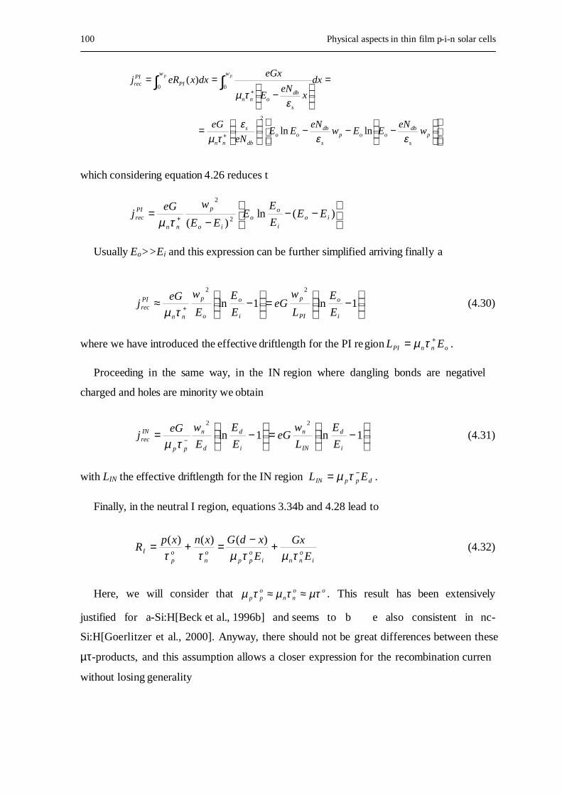
100 Physical aspects in thin film p-i-n solar cells
−−−
=
=
−
==
+
+∫∫
p
s
dboop
s
dboo
db
s
nn
w
s
dbonn
w
PIPIrec
weN
EEweN
EEeN
eG
dx
xeN
E
eGxdxxeRj
pp
εεε
τµ
ετµ
lnln
)(
2
00
which considering equation 4.26 reduces t
−−
−= + )(ln
)( 2
2
ioi
oo
io
p
nn
PIrec EE
E
EE
EE
weGj
τµ
Usually Eo>>Ei and this expression can be further simplified arriving finally a
−=
−≈ + 1ln1ln
22
i
o
PI
p
i
o
o
p
nn
PIrec
E
E
L
weG
E
E
E
weGj
τµ (4.30)
where we have introduced the effective driftlength for the PI region onnPI EL += τµ .
Proceeding in the same way, in the IN region where dangling bonds are negativel
charged and holes are minority we obtain
−=
−= − 1ln1ln
22
i
d
IN
n
i
d
d
n
pp
INrec
E
E
L
weG
E
E
E
weGj
τµ (4.31)
with LIN the effective driftlength for the IN region dppIN EL −= τµ .
Finally, in the neutral I region, equations 3.34b and 4.28 lead to
ionni
opp
on
op
IE
Gx
E
xdGxnxpR
τµτµττ+−=+= )()()(
(4.32)
Here, we will consider that oonn
opp µττµτµ ≈≈ . This result has been extensively
justified for a-Si:H[Beck et al., 1996b] and seems to b e also consistent in nc-
Si:H[Goerlitzer et al., 2000]. Anyway, there should not be great differences between these
µτ-products, and this assumption allows a closer expression for the recombination curren
without losing generality
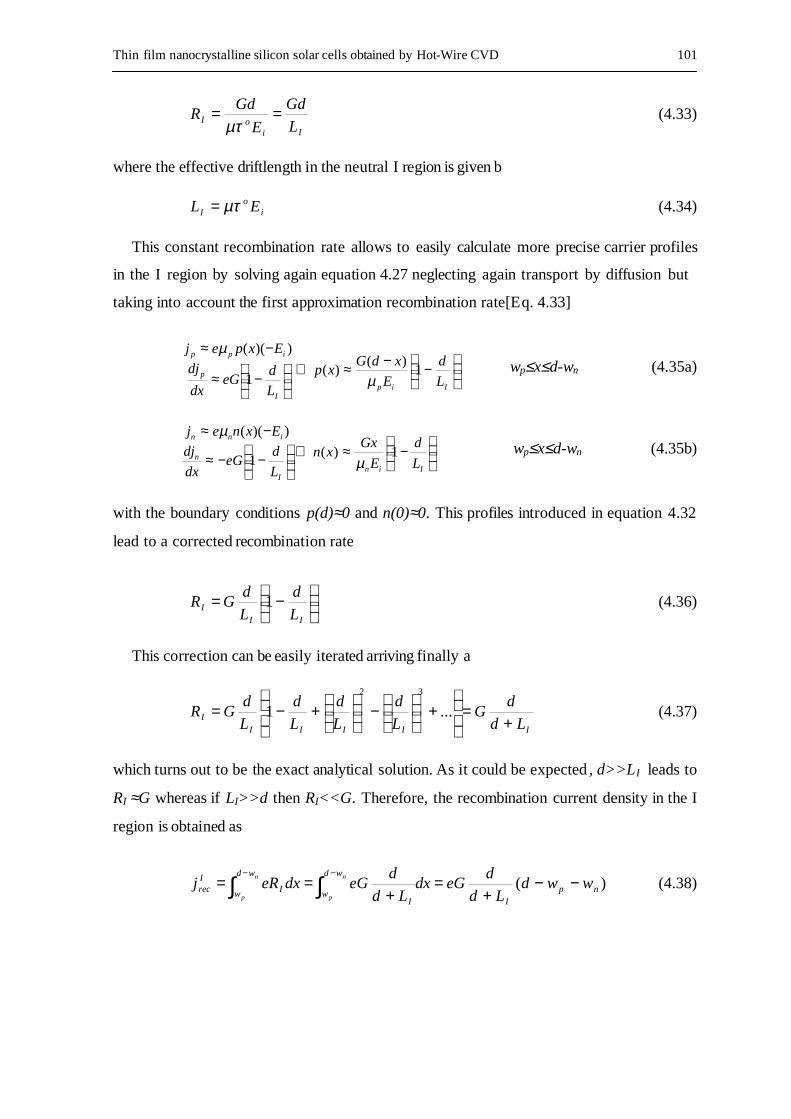
Thin film nanocrystalline silicon solar cells obtained by Hot-Wire CVD 101
IioI
L
Gd
E
GdR ==
µτ (4.33)
where the effective driftlength in the neutral I region is given b
io
I EL µτ= (4.34)
This constant recombination rate allows to easily calculate more precise carrier profiles
in the I region by solving again equation 4.27 neglecting again transport by diffusion but
taking into account the first approximation recombination rate[Eq. 4.33]
−−≈⇒
−≈
−≈
IipI
p
ipp
L
d
E
xdGxp
L
deG
dx
dj
Expej
1)(
)(1
))((
µ
µ wp≤x≤d-wn (4.35a)
−≈⇒
−−≈
−≈
IinI
n
inn
L
d
E
Gxxn
L
deG
dx
dj
Exnej
1)(1
))((
µ
µ wp≤x≤d-wn (4.35b)
with the boundary conditions p(d)≈0 and n(0)≈0. This profiles introduced in equation 4.32
lead to a corrected recombination rate
−=
III
L
d
L
dGR 1 (4.36)
This correction can be easily iterated arriving finally a
IIIII
ILd
dG
L
d
L
d
L
d
L
dGR
+=
+
−
+−= ...1
32
(4.37)
which turns out to be the exact analytical solution. As it could be expected , d>>LI leads to
RI ≈G whereas if LI>>d then RI<<G. Therefore, the recombination current density in the I
region is obtained as
)( npI
wd
wI
wd
w IIrec wwd
Ld
deGdx
Ld
deGdxeRj
n
p
n
p
−−+
=+
== ∫∫−−
(4.38)
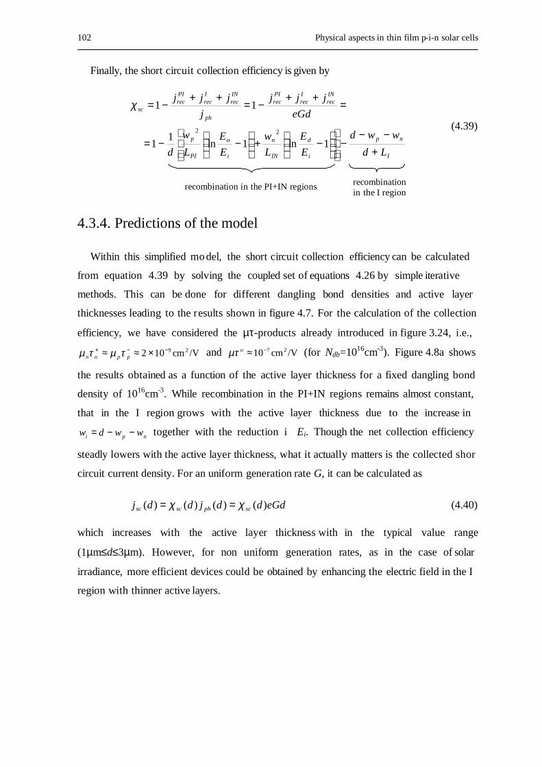
102 Physical aspects in thin film p-i-n solar cells
Finally, the short circuit collection efficiency is given by
I
np
i
d
IN
n
i
o
PI
p
INrec
Irec
PIrec
ph
INrec
Irec
PIrec
sc
Ld
wwd
E
E
L
w
E
E
L
w
d
eGd
jjj
j
jjj
+−−
−
−+
−−=
=++
−=++
−=
1ln1ln1
1
11
22
χ
(4.39)
4.3.4. Predictions of the model
Within this simplified mo del, the short circuit collection efficiency can be calculated
from equation 4.39 by solving the coupled set of equations 4.26 by simple iterative
methods. This can be done for different dangling bond densities and active layer
thicknesses leading to the results shown in figure 4.7. For the calculation of the collection
efficiency, we have considered the µτ-products already introduced in figure 3.24, i.e.,
/Vcm102 29−−+ ×≈≈ ppnn τµτµ and /Vcm10 27−≈oµτ (for Ndb=1016cm-3). Figure 4.8a shows
the results obtained as a function of the active layer thickness for a fixed dangling bond
density of 1016cm-3. While recombination in the PI+IN regions remains almost constant,
that in the I region grows with the active layer thickness due to the increase in
npi wwdw −−= together with the reduction i Ei. Though the net collection efficiency
steadly lowers with the active layer thickness, what it actually matters is the collected shor
circuit current density. For an uniform generation rate G, it can be calculated as
eGdddjddj scphscsc )()()()( χχ == (4.40)
which increases with the active layer thickness with in the typical value range
(1µm≤d≤3µm). However, for non uniform generation rates, as in the case of solar
irradiance, more efficient devices could be obtained by enhancing the electric field in the I
region with thinner active layers.
recombination in the PI+IN regions recombination in the I region
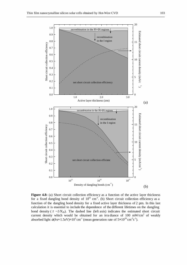
Thin film nanocrystalline silicon solar cells obtained by Hot-Wire CVD 103
1.0 2.0 3.00.0
0.1
0.2
0.3
0.4
0.5
0.6
0.7
0.8
0.9
1.0
net short circuit collection efficiency
recombination in the I region
recombination in the PI+IN regions Estim
ated short circuit current density (mA
/c2 )
Active layer thickness (µm)
Sho
rt c
ircu
it co
llect
ion
effi
cien
cy
0
5
10
15
20
(a)
1015 1016 10170.0
0.1
0.2
0.3
0.4
0.5
0.6
0.7
0.8
0.9
1.0
net short circuit collection efficienc
recombination in the I region
recombination in the PI+IN regions
Estim
ated short circuit current density (mA
/cm2 )
Density of dangling bonds (cm-3
)
Shor
t cir
cuit
colle
ctio
n ef
fici
ency
0
5
10
15
20
(b)
Figure 4.8: (a) Short circuit collection efficiency as a function of the active layer thickness for a fixed dangling bond density of 1016 cm-3. (b) Short circuit collection efficiency as a function of the dangling bond density for a fixed active layer thickness of 2 µm. In this last calculation it is essential to include the dependence of the different lifetimes on the dangling bond density ( τ ~1/Ndb). The dashed line (left axis) indicates the estimated short circuit current density which would be obtained for an irra diance of 100 mW/cm2 of weakly absorbed light α(hν=1.5eV)≈103 cm-1 (mean generation rate of 5×1020 cm-3s-1).
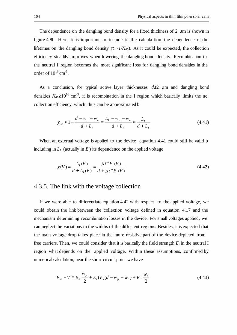
104 Physical aspects in thin film p-i-n solar cells
The dependence on the dangling bond density for a fixed thickness of 2 µm is shown in
figure 4.8b. Here, it is important to include in the calcula tion the dependence of the
lifetimes on the dangling bond density (τ ~1/Ndb). As it could be expected, the collection
efficiency steadily improves when lowering the dangling bond density. Recombination in
the neutral I region becomes the most significant loss for dangling bond densities in the
order of 1016 cm-3.
As a conclusion, for typical active layer thicknesses d≥2 µm and dangling bond
densities Ndb≥1016 cm-3, it is recombination in the I region which basically limits the ne
collection efficiency, which thus can be approximated b
I
I
I
npI
I
np
scLd
L
Ld
wwL
Ld
wwd
+≈
+−−
=+−−
−≈1χ (4.41)
When an external voltage is applied to the device, equation 4.41 could still be valid b
including in LI (actually in Ei) its dependence on the applied voltage
)(
)(
)(
)()(
VEd
VE
VLd
VLV
io
io
I
I
µτµτ
χ+
=+
= (4.42)
4.3.5. The link with the voltage collection
If we were able to differentiate equation 4.42 with respect to the applied voltage, we
could obtain the link between the collection voltage defined in equation 4.17 and the
mechanism determining recombination losses in the device. For small voltages applied, we
can neglect the variations in the widths of the differ ent regions. Besides, it is expected that
the main voltage drop takes place in the more resistive part of the device depleted from
free carriers. Then, we could consider that it is basically the field strength Ei in the neutral I
region what depends on the applied voltage. Within these assumptions, confirmed by
numerical calculation, near the short circuit point we have
2))((
2n
dnpi
p
obi
wEwwdVE
wEVV +−−+=− (4.43)
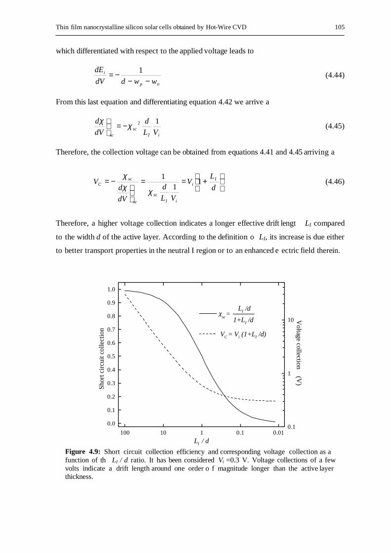
Thin film nanocrystalline silicon solar cells obtained by Hot-Wire CVD 105
which differentiated with respect to the applied voltage leads to
np
i
wwddV
dE
−−−= 1
(4.44)
From this last equation and differentiating equation 4.42 we arrive a
iIsc
sc VL
d
dV
d 12χχ−=
(4.45)
Therefore, the collection voltage can be obtained from equations 4.41 and 4.45 arriving a
+==
−=d
LV
VL
d
dV
dV I
i
iI
sc
sc
scC 1
11
χχχ
(4.46)
Therefore, a higher voltage collection indicates a longer effective drift lengt LI compared
to the width d of the active layer. According to the definition o LI, its increase is due either
to better transport properties in the neutral I region or to an enhanced e ectric field therein.
100 10 1 0.1 0.01
0.0
0.1
0.2
0.3
0.4
0.5
0.6
0.7
0.8
0.9
1.0
LI /d
1+LI /d χ
sc =
Voltage collection (V
)
LI / d
Shor
t cir
cuit
colle
ctio
n
0.1
1
10
VC = Vi (1+LI /d)
Figure 4.9: Short circuit collection efficiency and corresponding voltage collection as a function of th LI / d ratio. It has been considered Vi =0.3 V. Voltage collections of a few volts indicate a drift length around one order o f magnitude longer than the active layer thickness.
106 Physical aspects in thin film p-i-n solar cells
4.3.6. Contaminated devices
In the case of contaminated devices, we should take into account the non fully intrinsic
character of the active layer. Anyway, the Fer -level has to move across the band gap
throughout the active layer from the p- to the n-type doping levels. Hence, dangling bonds
will also change their state of charge depending on the position of the Fermi -level with
respect to the transition energy levels E+ and E-. However, a comparable or higher densit
of contaminants greatly perturbs the space charge density and thus the electric field profile.
The band diagram in the most usual case of n-type contaminants incorporated to the active
layer is shown in figure 4.10. For the calculation it was considered a deep distribution of
1016 cm-3 dangling bonds and a shallow distribution of 8×1015 cm-3 donors related t
contaminants 0.2 eV below the conduction band. This situation leads to EC-EF≈0.4 eV in
equilibrium which is similar to the dark conductivity activation energy measured in non
optimised undoped samples showing a pronounced n -type character. As in section 4.3.2,
three different regions can be distinguished depending on the sign of the space charge
density therein. However, now the space charge density is not due to just dangling bonds
which makes an analytical description much more complex.
a) PI region: The voltage drop Vp across this region is determined by the difference
between the equilibrium Fer -level positions in the p-doped and the undoped bu
contaminated active layer. Throughout this region the space charge density is positive
and screens the internal electric field strength until it completely vanishes. The
distribution of dangling bonds is positively charged only in the firs t tenth of micron
while in the rest of this region the space charge density is given by the concentration o
positively charged donors.
b) I region: Between the PI and IN regions extends a quasineutral region where the
positively charged donors are compensated by the fraction F- of negative dangling
bonds. By contrast to the case of an ideally intrinsic active layer, here the flat bands
indicate there is no voltage drop across this quasineutral region and thus the field
strength is null.
Thin film nanocrystalline silicon solar cells obtained by Hot-Wire CVD 107
c) IN region: Similarly to the PI region, the voltage drop Vn across this region is
determined by the difference between the equilibrium Fer -level positions in the n-
doped and the contaminated active layer. The space charge density throughout this
region is negative due to t he difference between the densities of negative dangling
bonds and positive donors. The density of free electrons in the conduction band can not
be neglected near the interface with the n -layer.
In this situation, the built-in voltage is given by the sum of the voltage drops in the
charged PI and IN regions whereas the voltage drop in the quasineutral I region can be
neglected. Besides, the main contribution is due to the PI region since Vp is significantly
higher than Vn. Actually, simulation shows that these devices behave as p -n junctions (i
fact p+-n-n+) instead of p-i-n structures.
0.0 0.2 0.4 0.6 0.8 1.0 1.2 1.4 1.6 1.8 2.0-1.0
-0.5
0.0
0.5
1.0
wn
wp
Vbi ≈ Vp+Vn
EV
EC
ED
EF
E-
E+
eVn
eVp
I region quasineutral
IN regionnegative
PI regionpositive
Position (µm)
Ban
d di
agra
m (
eV)
Figure 4.10: Calculated band diagram within the active layer of a contaminated (n -type) active layer. There is not a significant voltage drop across the quasineutral region (flat bands) where the field strength is null. The voltage drop in the PI region is significantly higher than that in the IN region. The device actually behaves as a p+-n-n+ structure.
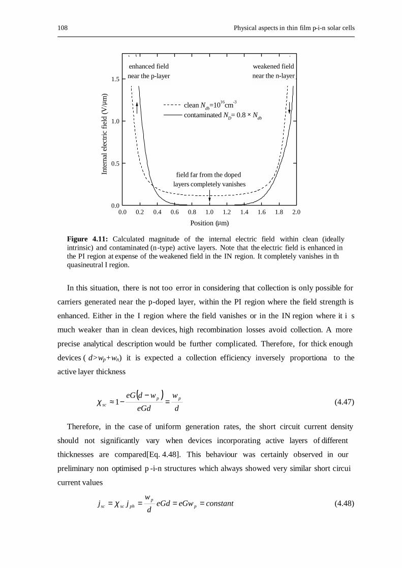
108 Physical aspects in thin film p-i-n solar cells
0.0 0.2 0.4 0.6 0.8 1.0 1.2 1.4 1.6 1.8 2.00.0
0.5
1.0
1.5
field far from the doped layers completely vanishes
weakened fieldnear the n-layer
enhanced fieldnear the p-layer
Position (µm)
Inte
rnal
ele
ctri
c fi
eld
(V/µ
m)
clean Ndb=1016
cm-3
contaminated ND= 0.8 × Ndb
Figure 4.11: Calculated magnitude of the internal electric field within clean (ideally intrinsic) and contaminated (n-type) active layers. Note that the electric field is enhanced in the PI region at expense of the weakened field in the IN region. It completely vanishes in thquasineutral I region.
In this situation, there is not too error in considering that collection is only possible for
carriers generated near the p-doped layer, within the PI region where the field strength is
enhanced. Either in the I region where the field vanishes or in the IN region where it i s
much weaker than in clean devices, high recombination losses avoid collection. A more
precise analytical description would be further complicated. Therefore, for thick enough
devices ( d>wp+wn) it is expected a collection efficiency inversely proportiona to the
active layer thickness
( )
d
w
eGd
wdeG pp
sc =−
−≈1χ (4.47)
Therefore, in the case of uniform generation rates, the short circuit current density
should not significantly vary when devices incorporating active layers of different
thicknesses are compared[Eq. 4.48]. This behaviour was certainly observed in our
preliminary non optimised p -i-n structures which always showed very similar short circui
current values
constanteGweGdd
wjj p
p
phscsc ==== χ (4.48)
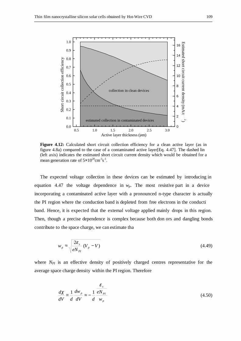
Thin film nanocrystalline silicon solar cells obtained by Hot-Wire CVD 109
0.5 1.0 1.5 2.0 2.5 3.00.0
0.1
0.2
0.3
0.4
0.5
0.6
0.7
0.8
0.9
1.0
collection in clean devices
estimated collection in contaminated devices
Estim
ated short circuit current density (mA
/c2 )
Active layer thickness (µm)
Shor
t cir
cuit
colle
ctio
n ef
fici
ency
0
2
4
6
8
10
12
14
16
Figure 4.12: Calculated short circuit collection efficiency for a clean active layer (as in figure 4.8a) compared to the case of a contaminated active layer[Eq. 4.47]. The dashed lin(left axis) indicates the estimated short circuit current density which would be obtained for a mean generation rate of 5×1020cm-3s-1.
The expected voltage collection in these devices can be estimated by introducing in
equation 4.47 the voltage dependence in wp. The most resistive part in a device
incorporating a contaminated active layer with a pronounced n-type character is actually
the PI region where the conduction band is depleted from free electrons in the conducti
band. Hence, it is expected that the external voltage applied mainly drops in this region.
Then, though a precise dependence is complex because both don ors and dangling bonds
contribute to the space charge, we can estimate tha
)(2
VVeN
w pPI
sp −≈
ε (4.49)
where NPI is an effective density of positively charged centres representative for the
average space charge density within the PI region. Therefore
p
PI
s
p
w
eN
ddV
dw
ddV
d
εχ 11 −≈= (4.50)
110 Physical aspects in thin film p-i-n solar cells
) pscps
PI
sc
scC Vw
eN
dV
dV 22 ==
−=εχ
χ (4.51)
Typical voltage drops around 0.5 V are expected in the PI region of devices
incorporating contaminated active layers[Fig. 4.10]. This would lead to voltage collections
slightly higher than 1 V in full agreement with our VIM measurements for solar cells
grown under non optimised deposition conditions.
Thin film nanocrystalline silicon solar cells obtained by Hot-Wire CVD 111
Chapter 5 Nanocrystalline silicon solar cells by HWCVD. Technological aspects
In this chapter we will consider some subjects which must be taken into account to
fabricate thin film solar cells. Technological aspects such as the selection of a suitable
front electrode or a method to reduce lateral leakage currents are considered. Besides, a
comprehensive study of the p-i-n devices obtained by HWCVD during the period of
research within the project Crystalline Silicon Solar Cells on Low Temperature Substrates
CRYSTAL (JOR3-CT97-0126) is presented.
5.1. Previous technological aspects 5.1.1. Selection of the TCO
In most thin film solar cells, the carrier on which the various thin film materials are
deposited, usually glass, also serves as a window to the cell. The front electrode usually
consists in a transparent conductive oxide (TCO) layer directly deposited onto the
carrier[Fig. 5.1]. The most common ones are aluminium-doped zinc oxide or AZO
(ZnO:Al), tin-doped indium oxide or ITO (In2O3:Sn) and fluorine-doped tin oxide or FTO
(SnO2:F). The requirements for the electrode material are[Schropp et al., 1998]: a) high transmission (preferably>85%) in the entire wavelength region where the
photovoltaic absorber layers are active b) low sheet resistance (preferably<10Ω/!) to minimise series resistance losses c) low contact resistance with the p-type layer of the p-i-n structure d) rough surface to increase the optical path of the light by scattering, while the
morphology should be such that shunting paths or pinholes are avoided e) chemical resistance against the strongly reducing hydrogen ambient during chemical
vapour deposition f) high thermal stability to avoid diffusion of elements into the growing layer
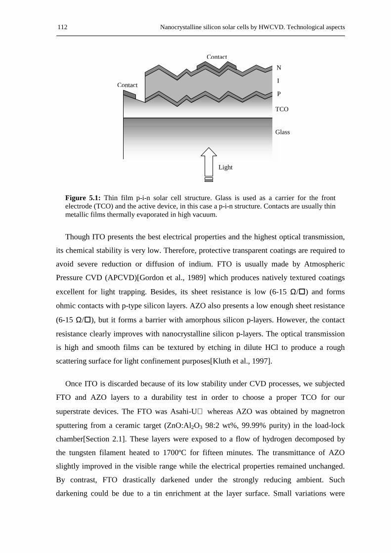
112 Nanocrystalline silicon solar cells by HWCVD. Technological aspects
Figure 5.1: Thin film p-i-n solar cell structure. Glass is used as a carrier for the front electrode (TCO) and the active device, in this case a p-i-n structure. Contacts are usually thin metallic films thermally evaporated in high vacuum.
Though ITO presents the best electrical properties and the highest optical transmission,
its chemical stability is very low. Therefore, protective transparent coatings are required to
avoid severe reduction or diffusion of indium. FTO is usually made by Atmospheric
Pressure CVD (APCVD)[Gordon et al., 1989] which produces natively textured coatings
excellent for light trapping. Besides, its sheet resistance is low (6-15 Ω/!) and forms
ohmic contacts with p-type silicon layers. AZO also presents a low enough sheet resistance
(6-15 Ω/!), but it forms a barrier with amorphous silicon p-layers. However, the contact
resistance clearly improves with nanocrystalline silicon p-layers. The optical transmission
is high and smooth films can be textured by etching in dilute HCl to produce a rough
scattering surface for light confinement purposes[Kluth et al., 1997].
Once ITO is discarded because of its low stability under CVD processes, we subjected
FTO and AZO layers to a durability test in order to choose a proper TCO for our
superstrate devices. The FTO was Asahi-U whereas AZO was obtained by magnetron
sputtering from a ceramic target (ZnO:Al2O3 98:2 wt%, 99.99% purity) in the load-lock
chamber[Section 2.1]. These layers were exposed to a flow of hydrogen decomposed by
the tungsten filament heated to 1700ºC for fifteen minutes. The transmittance of AZO
slightly improved in the visible range while the electrical properties remained unchanged.
By contrast, FTO drastically darkened under the strongly reducing ambient. Such
darkening could be due to a tin enrichment at the layer surface. Small variations were
Light
Contact
Contact
TCO Glass
N
I
P
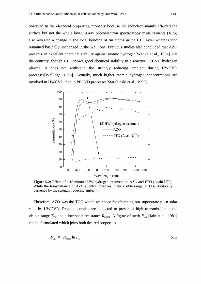
Thin film nanocrystalline silicon solar cells obtained by Hot-Wire CVD 113
observed in the electrical properties, probably because the reduction mainly affected the
surface but not the whole layer. X-ray photoelectron spectroscopy measurements (XPS)
also revealed a change in the local bonding of tin atoms in the FTO layer whereas zinc
remained basically unchanged in the AZO one. Previous studies also concluded that AZO
presents an excellent chemical stability against atomic hydrogen[Wanka et al., 1994]. On
the contrary, though FTO shows good chemical stability in a reactive PECVD hydrogen
plasma, it does not withstand the strongly reducing ambient during HWCVD
processes[Wallinga, 1998]. Actually, much higher atomic hydrogen concentrations are
involved in HWCVD than in PECVD processes[Starobinski et al., 1995].
300 400 500 600 700 800 900 1000 11000
10
20
30
40
50
60
70
80
90
100
15' HW hydrogen treatment
AZO
FTO (Asahi-UTM)
Wavelength (nm)
Tran
smitt
ance
(%)
Figure 5.2: Effect of a 15 minutes HW hydrogen treatment on AZO and FTO (Asahi-U ). While the transmittance of AZO slightly improves in the visible range, FTO is drastically darkened by the strongly reducing ambient.
Therefore, AZO was the TCO which we chose for obtaining our superstrate p-i-n solar
cells by HWCVD. Front electrodes are expected to present a high transmission in the
visible range Tvis and a low sheet resistance Rsheet. A figure of merit FJK [Jain et al., 1981]
can be formulated which joins both desired properties
vissheetJK TRF ln−= (5.1)
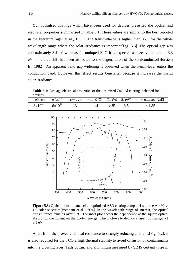
114 Nanocrystalline silicon solar cells by HWCVD. Technological aspects
Our optimised coatings which have been used for devices presented the optical and
electrical properties summarised in table 5.1. These values are similar to the best reported
in the literature[Jäger et al., 1998]. The transmittance is higher than 85% for the whole
wavelength range where the solar irradiance is important[Fig. 5.3]. The optical gap was
approximately 3.5 eV whereas for undoped ZnO it is expected a lower value around 3.3
eV. This blue shift has been attributed to the degeneration of the semiconductor[Burstein
E., 1982]. An apparent band gap widening is observed when the Fermi-level enters the
conduction band. However, this effect results beneficial because it increases the useful
solar irradiance.
Table 5.1: Average electrical properties of the optimised ZnO:Al coatings selected for devices. ρ (Ω cm) n (cm-3) µ (cm2/Vs) Rsheet (Ω/!) Tvis (%) Eg (eV) FJK=-Rsheet lnT (Ω/!)
8x10⁻⁴ 6x10²⁰ 13 11.4 >85 3.5 <1.85
300 400 500 600 700 800 900 1000
0
10
20
30
40
50
60
70
80
90
100
Wavelength (nm)
Tran
smitt
ance
(%)
0.00
0.01
0.02
0.03
0.04
0.05
0.06
0.07
0.08
Air M
ass 1.5 (mA
cm-2 nm
-1)
3.1 3.3 3.5 3.70
1
2
3
hν (eV)
α2 (×10
9 ) (c
m-2)
Figure 5.3: Optical transmittance of an optimised AZO coating compared with the Air Mass 1.5 solar spectrum[Wenham et al., 1994]. In the wavelength range of interest, the optical transmittance remains over 85%. The inset plot shows the dependence of the square optical absorption coefficient on the photon energy, which allows to deduce a direct optical gap of 3.5 eV.
Apart from the proved chemical resistance to strongly reducing ambients[Fig. 5.2], it
is also required for the TCO a high thermal stability to avoid diffusion of contaminants
into the growing layer. Tails of zinc and aluminium measured by SIMS certainly rise in
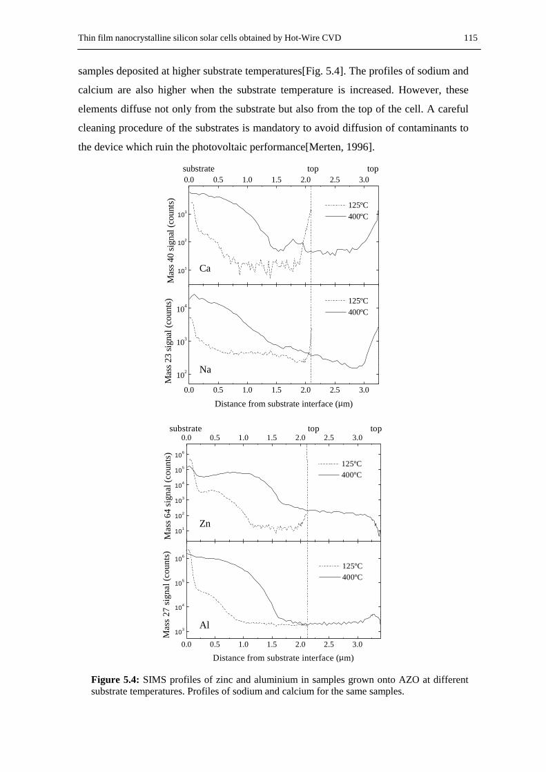
Thin film nanocrystalline silicon solar cells obtained by Hot-Wire CVD 115
samples deposited at higher substrate temperatures[Fig. 5.4]. The profiles of sodium and
calcium are also higher when the substrate temperature is increased. However, these
elements diffuse not only from the substrate but also from the top of the cell. A careful
cleaning procedure of the substrates is mandatory to avoid diffusion of contaminants to
the device which ruin the photovoltaic performance[Merten, 1996].
101
102
103
0.0 0.5 1.0 1.5 2.0 2.5 3.0
125ºC 400ºC
125ºC 400ºC
Mas
s 40
signa
l (co
unts)
0.0 0.5 1.0 1.5 2.0 2.5 3.0
102
103
104
top topsubstrate
Distance from substrate interface (µm)
Mas
s 23
signa
l (co
unts)
0.0 0.5 1.0 1.5 2.0 2.5 3.0103
104
105
106
top topsubstrate
Distance from substrate interface (µm)
Mas
s 27
sign
al (c
ount
s)
101
102
103
104
105
106
0.0 0.5 1.0 1.5 2.0 2.5 3.0
125ºC 400ºC
125ºC 400ºC
Mas
s 64
sign
al (c
ount
s)
Figure 5.4: SIMS profiles of zinc and aluminium in samples grown onto AZO at different substrate temperatures. Profiles of sodium and calcium for the same samples.
Ca Na Zn Al
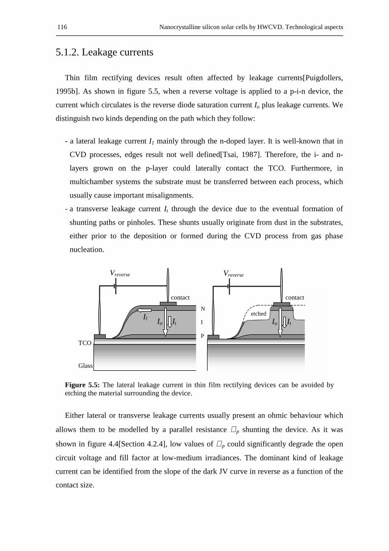
116 Nanocrystalline silicon solar cells by HWCVD. Technological aspects
5.1.2. Leakage currents
Thin film rectifying devices result often affected by leakage currents[Puigdollers,
1995b]. As shown in figure 5.5, when a reverse voltage is applied to a p-i-n device, the
current which circulates is the reverse diode saturation current Io plus leakage currents. We
distinguish two kinds depending on the path which they follow:
- a lateral leakage current I1 mainly through the n-doped layer. It is well-known that in
CVD processes, edges result not well defined[Tsai, 1987]. Therefore, the i- and n-
layers grown on the p-layer could laterally contact the TCO. Furthermore, in
multichamber systems the substrate must be transferred between each process, which
usually cause important misalignments.
- a transverse leakage current It through the device due to the eventual formation of
shunting paths or pinholes. These shunts usually originate from dust in the substrates,
either prior to the deposition or formed during the CVD process from gas phase
nucleation.
Figure 5.5: The lateral leakage current in thin film rectifying devices can be avoided by etching the material surrounding the device.
Either lateral or transverse leakage currents usually present an ohmic behaviour which
allows them to be modelled by a parallel resistance ℜ p shunting the device. As it was
shown in figure 4.4[Section 4.2.4], low values of ℜ p could significantly degrade the open
circuit voltage and fill factor at low-medium irradiances. The dominant kind of leakage
current can be identified from the slope of the dark JV curve in reverse as a function of the
contact size.
TCO Glass
Io It Il
Vreverse
N I P
Vreverse
Io It
contact contact
etched
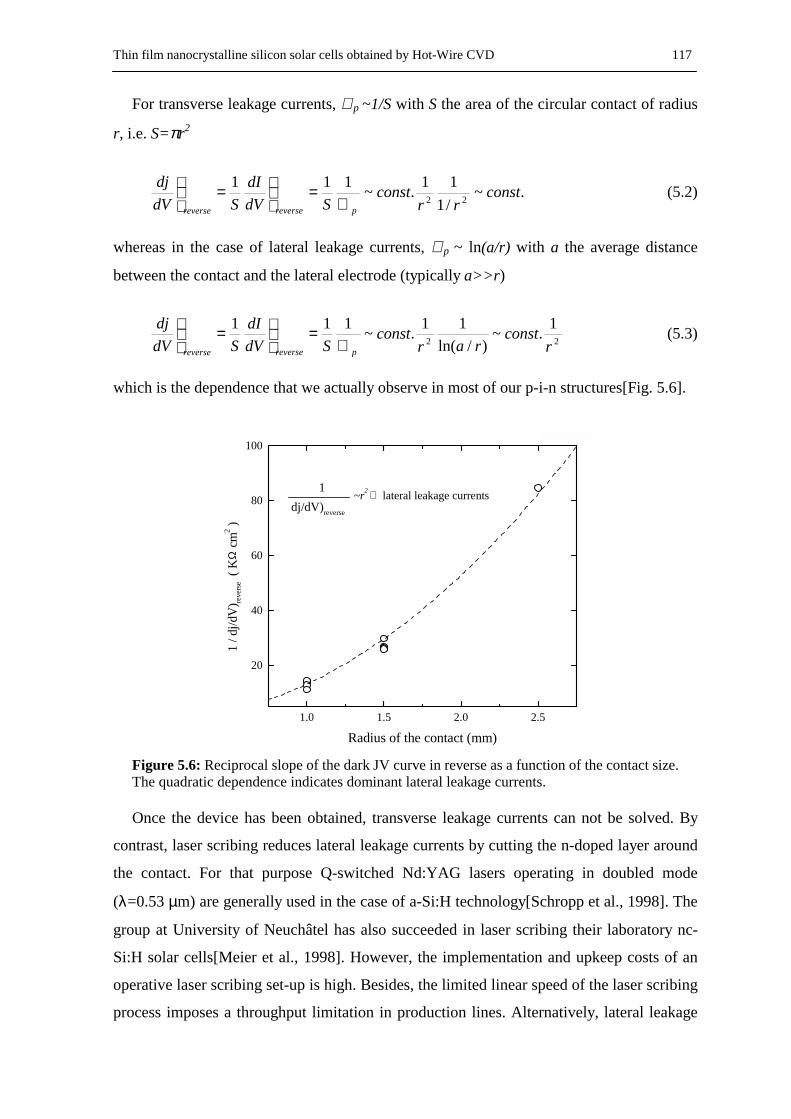
Thin film nanocrystalline silicon solar cells obtained by Hot-Wire CVD 117
For transverse leakage currents, ℜ p ~1/S with S the area of the circular contact of radius
r, i.e. S=πr2
.~/111.~111
22 constrr
constSdV
dISdV
dj
preversereverse ℜ=
=
(5.2)
whereas in the case of lateral leakage currents, ℜ p ~ ln(a/r) with a the average distance
between the contact and the lateral electrode (typically a>>r)
22
1.~)/ln(
11.~111r
constrar
constSdV
dISdV
dj
preversereverse ℜ=
=
(5.3)
which is the dependence that we actually observe in most of our p-i-n structures[Fig. 5.6].
1.0 1.5 2.0 2.5
20
40
60
80
100
1dj/dV)reverse
~r2 ⇒ lateral leakage currents
Radius of the contact (mm)
1 / d
j/dV
) reve
rse
( KΩ
cm
2 )
Figure 5.6: Reciprocal slope of the dark JV curve in reverse as a function of the contact size. The quadratic dependence indicates dominant lateral leakage currents.
Once the device has been obtained, transverse leakage currents can not be solved. By
contrast, laser scribing reduces lateral leakage currents by cutting the n-doped layer around
the contact. For that purpose Q-switched Nd:YAG lasers operating in doubled mode
(λ=0.53 µm) are generally used in the case of a-Si:H technology[Schropp et al., 1998]. The
group at University of Neuchâtel has also succeeded in laser scribing their laboratory nc-
Si:H solar cells[Meier et al., 1998]. However, the implementation and upkeep costs of an
operative laser scribing set-up is high. Besides, the limited linear speed of the laser scribing
process imposes a throughput limitation in production lines. Alternatively, lateral leakage
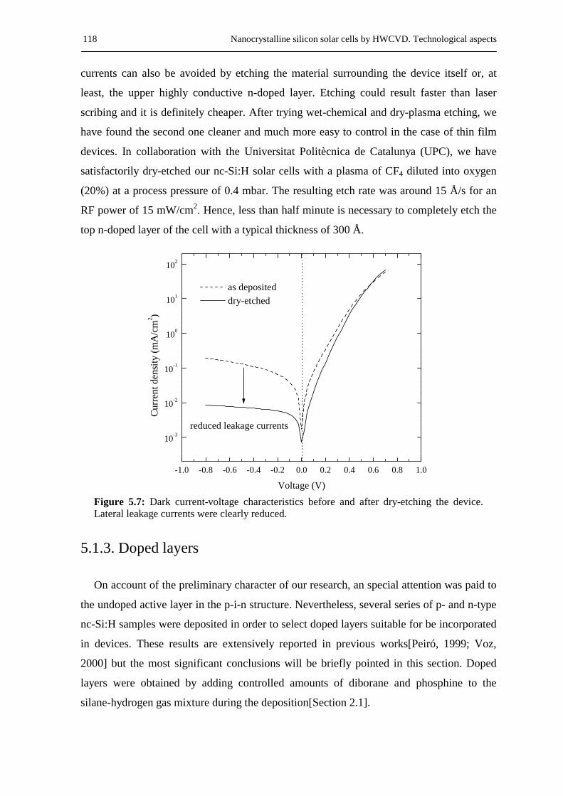
118 Nanocrystalline silicon solar cells by HWCVD. Technological aspects
currents can also be avoided by etching the material surrounding the device itself or, at
least, the upper highly conductive n-doped layer. Etching could result faster than laser
scribing and it is definitely cheaper. After trying wet-chemical and dry-plasma etching, we
have found the second one cleaner and much more easy to control in the case of thin film
devices. In collaboration with the Universitat Politècnica de Catalunya (UPC), we have
satisfactorily dry-etched our nc-Si:H solar cells with a plasma of CF4 diluted into oxygen
(20%) at a process pressure of 0.4 mbar. The resulting etch rate was around 15 Å/s for an
RF power of 15 mW/cm2. Hence, less than half minute is necessary to completely etch the
top n-doped layer of the cell with a typical thickness of 300 Å.
-1.0 -0.8 -0.6 -0.4 -0.2 0.0 0.2 0.4 0.6 0.8 1.0
10-3
10-2
10-1
100
101
102
reduced leakage currents
as deposited dry-etched
Voltage (V)
Curre
nt d
ensit
y (m
A/c
m2 )
Figure 5.7: Dark current-voltage characteristics before and after dry-etching the device. Lateral leakage currents were clearly reduced.
5.1.3. Doped layers
On account of the preliminary character of our research, an special attention was paid to
the undoped active layer in the p-i-n structure. Nevertheless, several series of p- and n-type
nc-Si:H samples were deposited in order to select doped layers suitable for be incorporated
in devices. These results are extensively reported in previous works[Peiró, 1999; Voz,
2000] but the most significant conclusions will be briefly pointed in this section. Doped
layers were obtained by adding controlled amounts of diborane and phosphine to the
silane-hydrogen gas mixture during the deposition[Section 2.1].
Thin film nanocrystalline silicon solar cells obtained by Hot-Wire CVD 119
N-type layers suitable for device applications were obtained with phosphorous to silicon
gas phase ratios in the order of 2%. The corresponding phosphorous to silicon solid phase
ratios estimated by SIMS were around 0.1% which results in a gas to solid phase
phosphorous incorporation efficiency of 5%. These layers presented room temperature
dark conductivities ranging from 1 to 10 Ω-1cm-1 and activation energies well below 0.1eV.
Any significant dependence was not observed within the typical substrate temperature
range (150-300ºC) or when the hydrogen dilution was increased from 90 to 95%. The
process pressure was around 10-2 mbar.
On the other hand, in the case of p-doped layers, boron to silicon solid phase ratios as
high as 1% were required to obtain room temperature dark conductivities ranging from 0.5
to 5 Ω-1cm-1 and activation energies below 0.1eV. These heavily p-doped layers could be
achieved for gas phase boron to silicon ratios in the order of 1%. Hence, the gas to solid
phase boron incorporation efficiency approached 100%. This result could be explained by
the well-known thermal dissociation of diborane[Tarui et al., 1989]. Whereas silane,
hydrogen or phosphine are only dissociated by the hot filament, diborane is additionally
dissociated at the hot surfaces inside the deposition chamber. Amorphisation at such high
p-type doping levels could be prevented by lowering the substrate temperature to 150ºC
and increasing the hydrogen dilution to 95%. The crystallinity enhancement for decreasing
substrate temperatures could seem surprising, since higher crystallinity is usually expected
when increasing the substrate temperature. However, this effect could be explained by
structural changes when less hydrogen is incorporated due to a higher substrate
temperature. Actually, it is well stablished that atomic hydrogen favours the crystalline
growth either by etching stressed bonds[Tsai et al., 1988] or increasing the diffusion length
of the growth precursors[Matsuda, 1983]. The process pressure remained unchanged
around 10-2 mbar.
The optimised doped layers could be scaled to thicknesses proper for devices
maintaining good structural and electrical properties. Our preliminar p-i-n structures
incorporate doped layers with typical thicknesses around 500 Å. This relatively high value
ensures good rectifying characteristics and prevents from shunting paths. However,
significant optical losses due to the absorption within the p-layer limit the maximum
expected efficiency of such devices[Section 3.1.3].
120 Nanocrystalline silicon solar cells by HWCVD. Technological aspects
5.2. The role of the active layer in the device performance 5.2.1. The microdoping approach
The incorporation of contaminants during the growth of the intrinsic layer of the p-i-n
structure not only increases the concentration of recombination centres, but also results in
the screening of the internal electric field. Both effects directly worsen the drift length[Eq.
4.2] and consequently the collection of photogenerated carriers. Therefore, the reduction of
contaminant sources is a major problem to be solve, specially in low pressure deposition
techniques such as PECVD or HWCVD. Many aspects can cause an undesired
contamination:
a) the cleanness of the chamber and the gas lines. The outgassing rate has to be
minimised as much as possible. Accessories inside the chamber must be specific for
high vacuum applications and an special care of the heater design must be taken
b) the cleanness of the substrates and its stability. Substrates must be degreased and
carefully cleaned. They must resist the deposition conditions without diffusing species
into the growing layer and they should not suffer chemical reactions which alter their
properties
c) the purity of the gas bottles. Often it is necessary to use additional gas purifiers or
selective gas getters to enhance the purity of the mixture which enters the deposition
chamber
d) the pumping system. A good base pressure is certainly necessary for electronic
applications and backstreaming has to be avoided
But sometimes contamination is intimately related to the deposition process. For
instance, the filament used in HWCVD is a potential source of tungsten contamination. In
such cases the only possibility is to try to minimise or, if possible, compensate its effects.
Conceptually, p-type microdoping could counterbalance the as grown n-type character of
nc-Si:H usually associated to oxygen contamination[Torres et al., 1996]. Actually, several
shallow donor levels (EC-ED≤0.14 eV) which could be attributed to oxygen were resolved
by DLTS in our samples[Stöger et al., 1999]. We have certainly found that low p-type
doping levels (~1019 cm-3) yield activation energies near midgap and lower room
temperature dark conductivities[Voz et al., 2000]. When this compensated samples are
Thin film nanocrystalline silicon solar cells obtained by Hot-Wire CVD 121
incorporated as active layers in p-i-n structures, the negatively charged acceptors due to the
boron incorporation compensate the positively charged donors due to contaminants. As a
result, there is a reduction in the charged trap density and consequently, the internal
electric field within the active layer is enhanced. This approach was first successfully
implemented in a nanocrystalline photovoltaic devices by the group at University of
Newchâtel[Meier et al., 1994]. We have also tried to obtain compensated p-i-n solar cells
by depositing the intrinsic layer with controlled low flows of diborane[Table 5.2].
Figure 5.8 compares the JV curves of a compensated and non compensated cell under
an irradiance of 100 mW/cm2. The short circuit current density is clearly raised in the
compensated cell whereas both fill factor and open circuit voltage are slightly better for the
non compensated device. Since diffusion is expected to play a more important role in the
non compensated device, it can be halfway between a p-i-n and a p-n (actually p+-n-n+)
structure, which would explain the improved open circuit voltage and fill factor.
Table 5.2: Compensated p-i-n structures compared with non compensated ones for different silane flows. The short circuit current and open circuit voltage were measured under an irradiance of 100 mW/cm2. They are grouped in low flow-non compensated, low flow- compensated, high flow-non compensated, high flow-overcompensated and high flow- compensated.
Cell name SiH4/H2 flows (sccm)
B/Si ratio (gas phase)
Thickness (µm)
jsc (mA/cm2)
Voc (V)
rd (Å/s)
981127c 1 / 19 0 2.4 5.5 0.26 1.6 990113c 1 / 19 0 1.4 5.6 0.28 1.7 990119c 1 / 19 10-4 0.96 9.1 0.25 0.8 990115c 1 / 19 10-4 1.06 7.8 0.23 0.9 990319c 4 / 76 0 2.15 6.42 0.27 3.6 990311c 4 / 76 10-4 2.5 1.51 0.16 2.4 990323c 4 / 76 10-5 2.1 9.5 0.25 2.5
In figure 5.9 we compare the spectral responses of compensated and non compensated
structures obtained with low gas flows. The compensated cell was not too far from the
optical limit for long wavelenghts while the non compensated one showed a much poorer
collection. Losses in the short wavelength range are mainly due to the optical absorption of
the p-doped layer and to interface recombination.
122 Nanocrystalline silicon solar cells by HWCVD. Technological aspects
0.0 0.1 0.2 0.3
-9
-8
-7
-6
-5
-4
-3
-2
-1
0
Irradiance of 100 mW/cm2
Power density (m
W/cm
2)
990113c non compensated 990119c compensated
Curre
nt d
ensit
y (m
A/c
m2 )
Voltage (V)
-2
-1
0
power outputs
JV curves
Figure 5.8: JV curves and power outputs for the compensated 990119c and non compensated 990113c p-i-n structures.
300 400 500 600 700 800 900 10000.0
0.1
0.2
0.3
0.4
0.5
0.6
0.7
0.8
0.9
1.0
bulk recombination due to short drift-length
optical losses
p-la
yer o
ptic
al a
bsor
ptio
nan
d in
terfa
ce re
com
bina
tion 990113c non compensated
990119c compensated
Ex
tern
al q
uant
um e
ffici
ency
Wavelength (nm) Figure 5.9: External quantum efficiency for the compensated 990119c and non compensated 990113c p-i-n structures. The estimated optical absorptances of these devices are also plotted.
Thin film nanocrystalline silicon solar cells obtained by Hot-Wire CVD 123
0.0 0.2 0.4 0.6 0.8 1.0 1.2 1.4 1.6 1.8 2.010-5
10-4
10-3
10-2
10-1
100
101
enhancement by compensation
screening due to thespace charge density
Position (µm)
Inte
rnal
ele
ctric
fiel
d (V
/µm
)
clean Ndb=1016cm-3
contaminated ND= 0.8 × Ndb 95% compensated ND= 0.8 × Ndb + NA= 0.95 × ND
Figure 5.10: Simulated internal field profile in equilibrium for a clean (not contaminated), contaminated (8×1015 cm-3 donors) and 95% compensated (7.6×1015 cm-3 acceptors) p-i-n structures.
Some calculations were done to get a further understanding of the results. Figure 5.10
shows the internal field profile in equilibrium obtained by numerical simulation for an
ideally clean, contaminated and compensated p-i-n structures. The density of dangling
bonds, estimated from PDS, was fixed to 1016cm-3 in any case whereas the concentration of
donors in the contaminated cell was chosen 8×1015 cm-3. The 95% compensated device was
simulated by adding an acceptor density of 7.6×1015 cm-3. Note the drastically screened
field of the non compensated cell. Though the field is more intense near the p-i (actually
p+-n) interface, in the middle of the active layer it is almost four orders of magnitude
weaker than in either the clean or the compensated cell. Therefore, electron-hole pairs
generated far from the interfaces are hardly separated by drift and only diffusion can help
to collect them. The low mobility of nanocrystalline silicon does not allow diffusion alone
to be enough to efficiently collect the photogenerated carriers[Section 4.1]. This fact
explains the low response for long wavelengths of non compensated p-i-n structures which
mainly collect those pairs generated near the p-i interface.
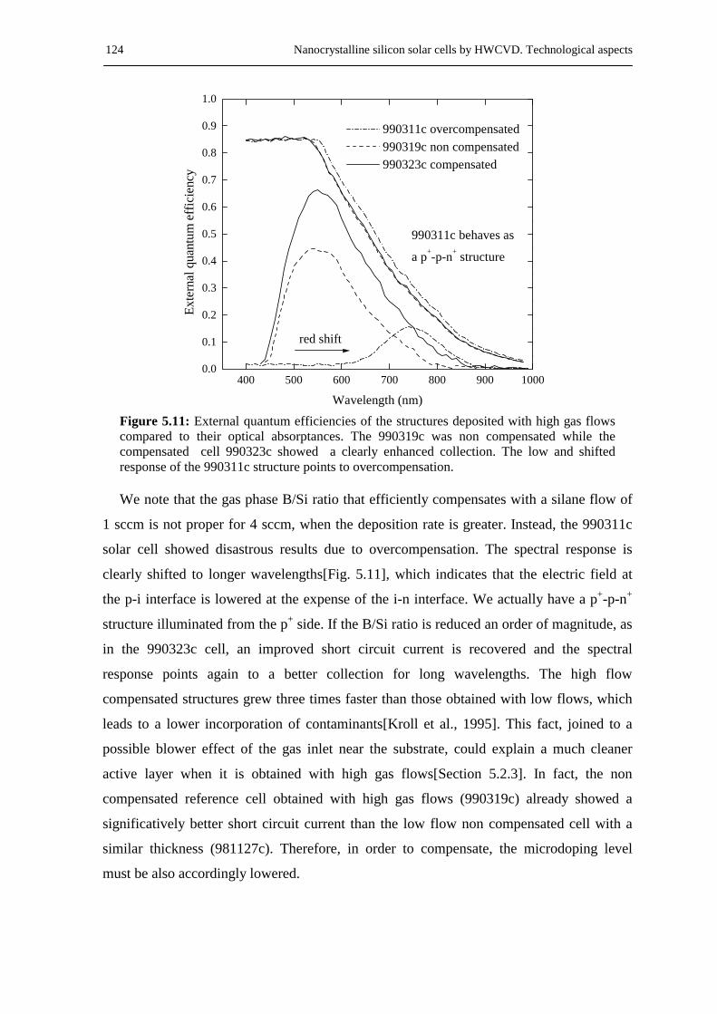
124 Nanocrystalline silicon solar cells by HWCVD. Technological aspects
400 500 600 700 800 900 10000.0
0.1
0.2
0.3
0.4
0.5
0.6
0.7
0.8
0.9
1.0
red shift
990311c behaves as
a p+-p-n+ structure
990311c overcompensated 990319c non compensated 990323c compensated
Wavelength (nm)
Exte
rnal
qua
ntum
effi
cien
cy
Figure 5.11: External quantum efficiencies of the structures deposited with high gas flows compared to their optical absorptances. The 990319c was non compensated while the compensated cell 990323c showed a clearly enhanced collection. The low and shifted response of the 990311c structure points to overcompensation.
We note that the gas phase B/Si ratio that efficiently compensates with a silane flow of
1 sccm is not proper for 4 sccm, when the deposition rate is greater. Instead, the 990311c
solar cell showed disastrous results due to overcompensation. The spectral response is
clearly shifted to longer wavelengths[Fig. 5.11], which indicates that the electric field at
the p-i interface is lowered at the expense of the i-n interface. We actually have a p+-p-n+
structure illuminated from the p+ side. If the B/Si ratio is reduced an order of magnitude, as
in the 990323c cell, an improved short circuit current is recovered and the spectral
response points again to a better collection for long wavelengths. The high flow
compensated structures grew three times faster than those obtained with low flows, which
leads to a lower incorporation of contaminants[Kroll et al., 1995]. This fact, joined to a
possible blower effect of the gas inlet near the substrate, could explain a much cleaner
active layer when it is obtained with high gas flows[Section 5.2.3]. In fact, the non
compensated reference cell obtained with high gas flows (990319c) already showed a
significatively better short circuit current than the low flow non compensated cell with a
similar thickness (981127c). Therefore, in order to compensate, the microdoping level
must be also accordingly lowered.
Thin film nanocrystalline silicon solar cells obtained by Hot-Wire CVD 125
5.2.2. Influence of the filament temperature
One of the main unsolved questions related to the HWCVD technique is the possibility
of tungsten incorporation into the growing layer. If it is present, tungsten contamination
should depend on the filament temperature. Concentrations of tungsten with clear
detrimental electronic effects are hardly detectable by compositional analysis, even for
most SIMS systems[Delgado et al., 1990]. By contrast, as it was pointed in section 3.2.4, a
higher density of charged centres is deduced from the depletion capacitance of pseudo-
Schottky contacts grown with higher filament temperatures. Besides, two donor levels
were resolved by DLTS which could be attributed to contamination with tungsten (EC-
ED=0.336eV) and interstitial cooper (EC-ED=0.185eV)[Stöger et al., 1999]. This last
element could come from impurities in the filament or more probably, from cooper parts of
the filament holder. Moreover, cooper could be also detected by SIMS in samples grown at
high filament temperatures. Therefore, several cells were obtained with exactly the same
technological parameters except for the temperature of the filament when the active layer
was grown[Table 5.3].
These cells were obtained paying special attention to the cleanness of the substrates and
the outgassing rate of the chamber in order to avoid any additional difference than the
filament temperature. Moreover, they were obtained consecutively, without any process
between them, in order to discard any evolution of the wire. Though devices obtained at
higher filament temperatures resulted slightly thicker due to a higher dissociation of the
gases, this very small difference should not be representative when comparing the
characteristics of the cells. By contrast, clear differences were observed in the photovoltaic
performance, which worsens when the filament temperature is increased. We observe a
more drastic effect at higher process pressures[Table 5.3], probably because these
conditions are more aggressive for the filament. We must consider that the tungsten
incorporation into the growing layer could be not only due to just evaporation from the
filament but also to chemical reactions with the growing precursors. X-ray diffraction of
filaments used in deposition processes evidenced the eventual formation of tungsten
silicides which certainly have a higher vapour pressure than clean tungsten.
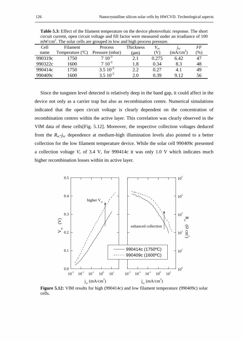
126 Nanocrystalline silicon solar cells by HWCVD. Technological aspects
Table 5.3: Effect of the filament temperature on the device photovoltaic response. The short circuit current, open circuit voltage and fill factor were measured under an irradiance of 100 mW/cm2. The solar cells are grouped in low and high process pressure. Cell name
Filament Temperature (ºC)
Process Pressure (mbar)
Thickness (µm)
Voc (V)
jsc (mA/cm2)
FF (%)
990319c 1750 7 10-3 2.1 0.275 6.42 47 990322c 1600 7 10-3 1.8 0.34 8.3 48 990414c 1750 3.5 10-2 2.2 0.27 4.1 49 990409c 1600 3.5 10-2 2.0 0.39 9.12 56
Since the tungsten level detected is relatively deep in the band gap, it could affect in the
device not only as a carrier trap but also as recombination centre. Numerical simulations
indicated that the open circuit voltage is clearly dependent on the concentration of
recombination centres within the active layer. This correlation was clearly observed in the
VIM data of these cells[Fig. 5.12]. Moreover, the respective collection voltages deduced
from the Rsc-jsc dependence at medium-high illumination levels also pointed to a better
collection for the low filament temperature device. While the solar cell 990409c presented
a collection voltage Vc of 3.4 V, for 990414c it was only 1.0 V which indicates much
higher recombination losses within its active layer.
10-3 10-2 10-1 100 1010.0
0.1
0.2
0.3
0.4
0.5
higher Voc
enhanced collection
Voc
(V
)
jsc (mA/cm2)
10-3 10-2 10-1 100 101100
101
102
103
104
105
990414c (1750ºC) 990409c (1600ºC)
jsc (mA/cm2)
Rsc ( Ω
cm2)
Figure 5.12: VIM results for high (990414c) and low filament temperature (990409c) solar cells.
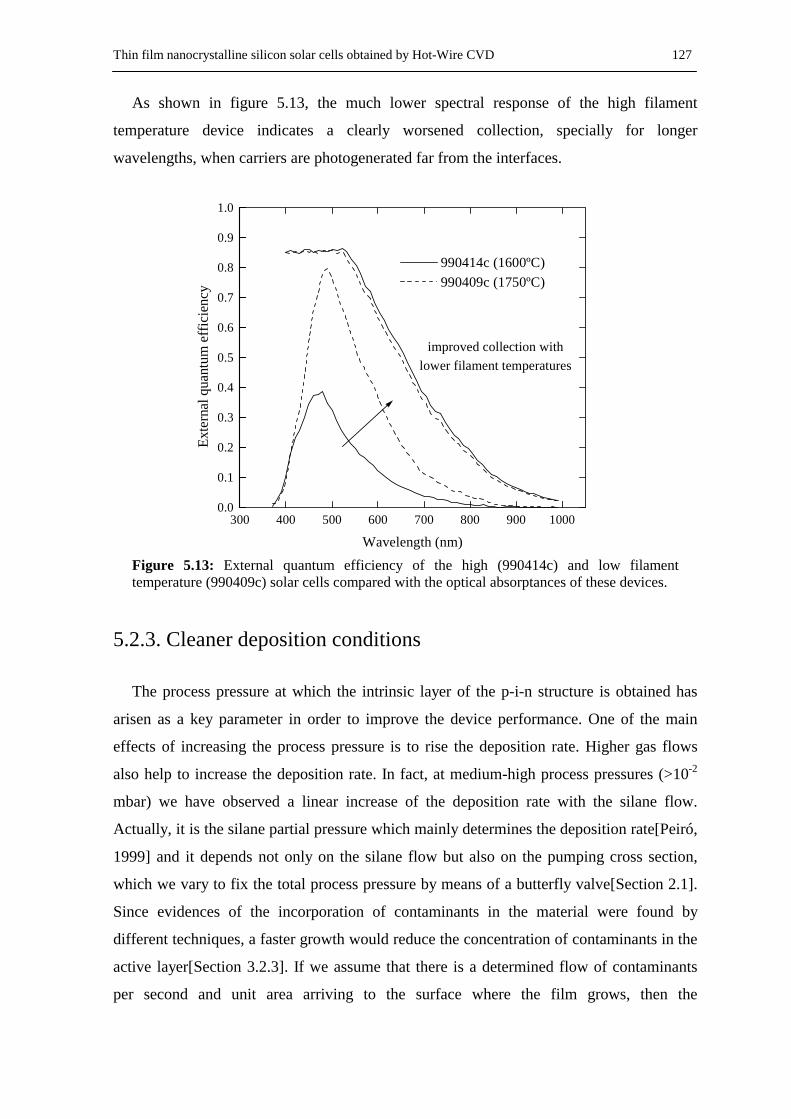
Thin film nanocrystalline silicon solar cells obtained by Hot-Wire CVD 127
As shown in figure 5.13, the much lower spectral response of the high filament
temperature device indicates a clearly worsened collection, specially for longer
wavelengths, when carriers are photogenerated far from the interfaces.
300 400 500 600 700 800 900 10000.0
0.1
0.2
0.3
0.4
0.5
0.6
0.7
0.8
0.9
1.0
improved collection withlower filament temperatures
990414c (1600ºC) 990409c (1750ºC)
Wavelength (nm)
Exte
rnal
qua
ntum
effi
cien
cy
Figure 5.13: External quantum efficiency of the high (990414c) and low filament temperature (990409c) solar cells compared with the optical absorptances of these devices.
5.2.3. Cleaner deposition conditions
The process pressure at which the intrinsic layer of the p-i-n structure is obtained has
arisen as a key parameter in order to improve the device performance. One of the main
effects of increasing the process pressure is to rise the deposition rate. Higher gas flows
also help to increase the deposition rate. In fact, at medium-high process pressures (>10-2
mbar) we have observed a linear increase of the deposition rate with the silane flow.
Actually, it is the silane partial pressure which mainly determines the deposition rate[Peiró,
1999] and it depends not only on the silane flow but also on the pumping cross section,
which we vary to fix the total process pressure by means of a butterfly valve[Section 2.1].
Since evidences of the incorporation of contaminants in the material were found by
different techniques, a faster growth would reduce the concentration of contaminants in the
active layer[Section 3.2.3]. If we assume that there is a determined flow of contaminants
per second and unit area arriving to the surface where the film grows, then the
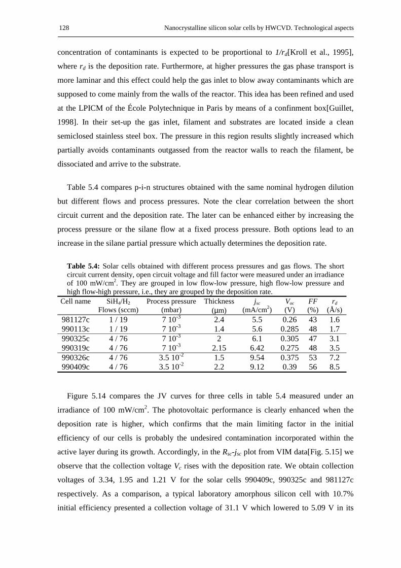
128 Nanocrystalline silicon solar cells by HWCVD. Technological aspects
concentration of contaminants is expected to be proportional to 1/rd[Kroll et al., 1995],
where rd is the deposition rate. Furthermore, at higher pressures the gas phase transport is
more laminar and this effect could help the gas inlet to blow away contaminants which are
supposed to come mainly from the walls of the reactor. This idea has been refined and used
at the LPICM of the École Polytechnique in Paris by means of a confinment box[Guillet,
1998]. In their set-up the gas inlet, filament and substrates are located inside a clean
semiclosed stainless steel box. The pressure in this region results slightly increased which
partially avoids contaminants outgassed from the reactor walls to reach the filament, be
dissociated and arrive to the substrate.
Table 5.4 compares p-i-n structures obtained with the same nominal hydrogen dilution
but different flows and process pressures. Note the clear correlation between the short
circuit current and the deposition rate. The later can be enhanced either by increasing the
process pressure or the silane flow at a fixed process pressure. Both options lead to an
increase in the silane partial pressure which actually determines the deposition rate.
Table 5.4: Solar cells obtained with different process pressures and gas flows. The short circuit current density, open circuit voltage and fill factor were measured under an irradiance of 100 mW/cm2. They are grouped in low flow-low pressure, high flow-low pressure and high flow-high pressure, i.e., they are grouped by the deposition rate.
Cell name SiH4/H2 Flows (sccm)
Process pressure (mbar)
Thickness (µm)
jsc (mA/cm2)
Voc (V)
FF (%)
rd (Å/s)
981127c 1 / 19 7 10-3 2.4 5.5 0.26 43 1.6 990113c 1 / 19 7 10-3 1.4 5.6 0.285 48 1.7 990325c 4 / 76 7 10-3 2 6.1 0.305 47 3.1 990319c 4 / 76 7 10-3 2.15 6.42 0.275 48 3.5 990326c 4 / 76 3.5 10-2 1.5 9.54 0.375 53 7.2 990409c 4 / 76 3.5 10-2 2.2 9.12 0.39 56 8.5
Figure 5.14 compares the JV curves for three cells in table 5.4 measured under an
irradiance of 100 mW/cm2. The photovoltaic performance is clearly enhanced when the
deposition rate is higher, which confirms that the main limiting factor in the initial
efficiency of our cells is probably the undesired contamination incorporated within the
active layer during its growth. Accordingly, in the Rsc-jsc plot from VIM data[Fig. 5.15] we
observe that the collection voltage Vc rises with the deposition rate. We obtain collection
voltages of 3.34, 1.95 and 1.21 V for the solar cells 990409c, 990325c and 981127c
respectively. As a comparison, a typical laboratory amorphous silicon cell with 10.7%
initial efficiency presented a collection voltage of 31.1 V which lowered to 5.09 V in its
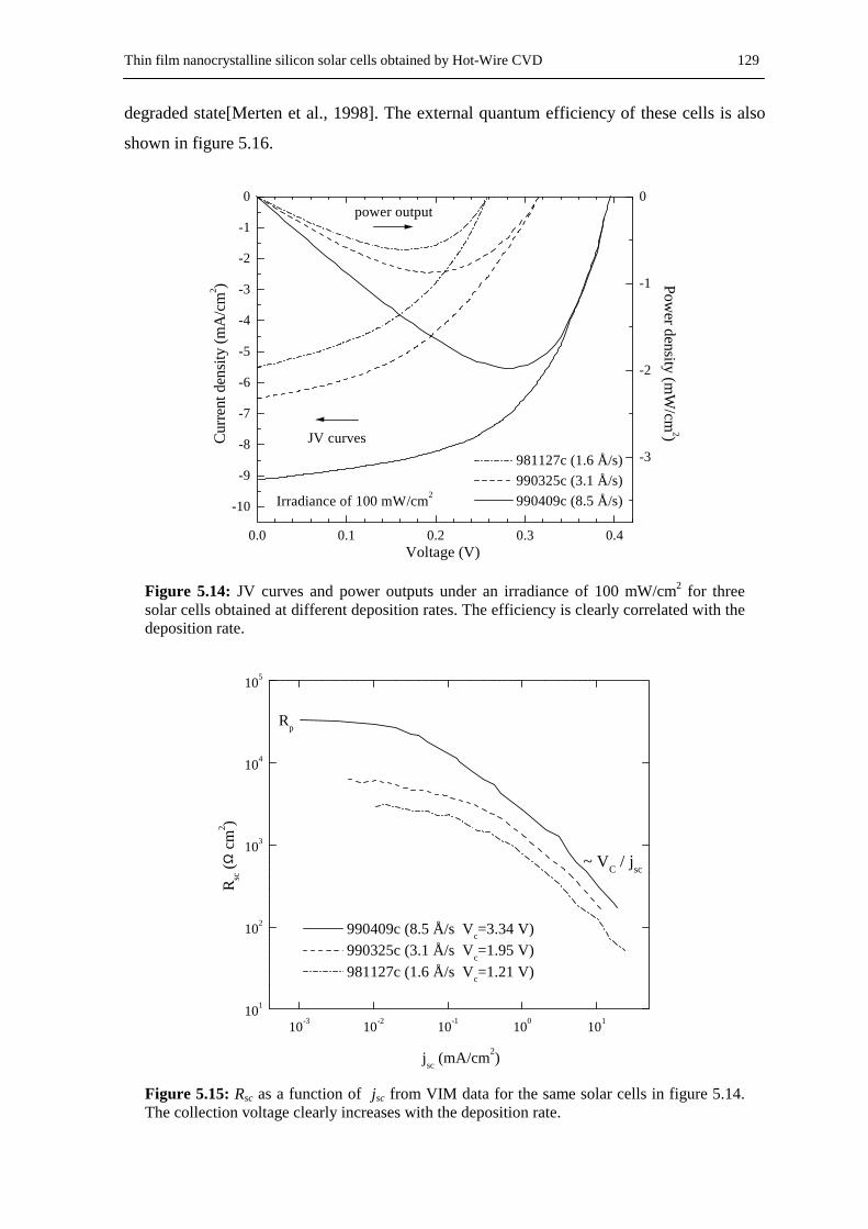
Thin film nanocrystalline silicon solar cells obtained by Hot-Wire CVD 129
degraded state[Merten et al., 1998]. The external quantum efficiency of these cells is also
shown in figure 5.16.
0.0 0.1 0.2 0.3 0.4
-10
-9
-8
-7
-6
-5
-4
-3
-2
-1
0
Irradiance of 100 mW/cm2
JV curves
power outputPow
er density (mW
/cm2)
981127c (1.6 Å/s) 990325c (3.1 Å/s) 990409c (8.5 Å/s)
Curre
nt d
ensit
y (m
A/c
m2 )
Voltage (V)
-3
-2
-1
0
Figure 5.14: JV curves and power outputs under an irradiance of 100 mW/cm2 for three solar cells obtained at different deposition rates. The efficiency is clearly correlated with the deposition rate.
10-3 10-2 10-1 100 101101
102
103
104
105
990409c (8.5 Å/s Vc=3.34 V) 990325c (3.1 Å/s Vc=1.95 V) 981127c (1.6 Å/s Vc=1.21 V)
Rp
~ VC / jsc
jsc (mA/cm2)
Rsc (Ω
cm
2 )
Figure 5.15: Rsc as a function of jsc from VIM data for the same solar cells in figure 5.14. The collection voltage clearly increases with the deposition rate.
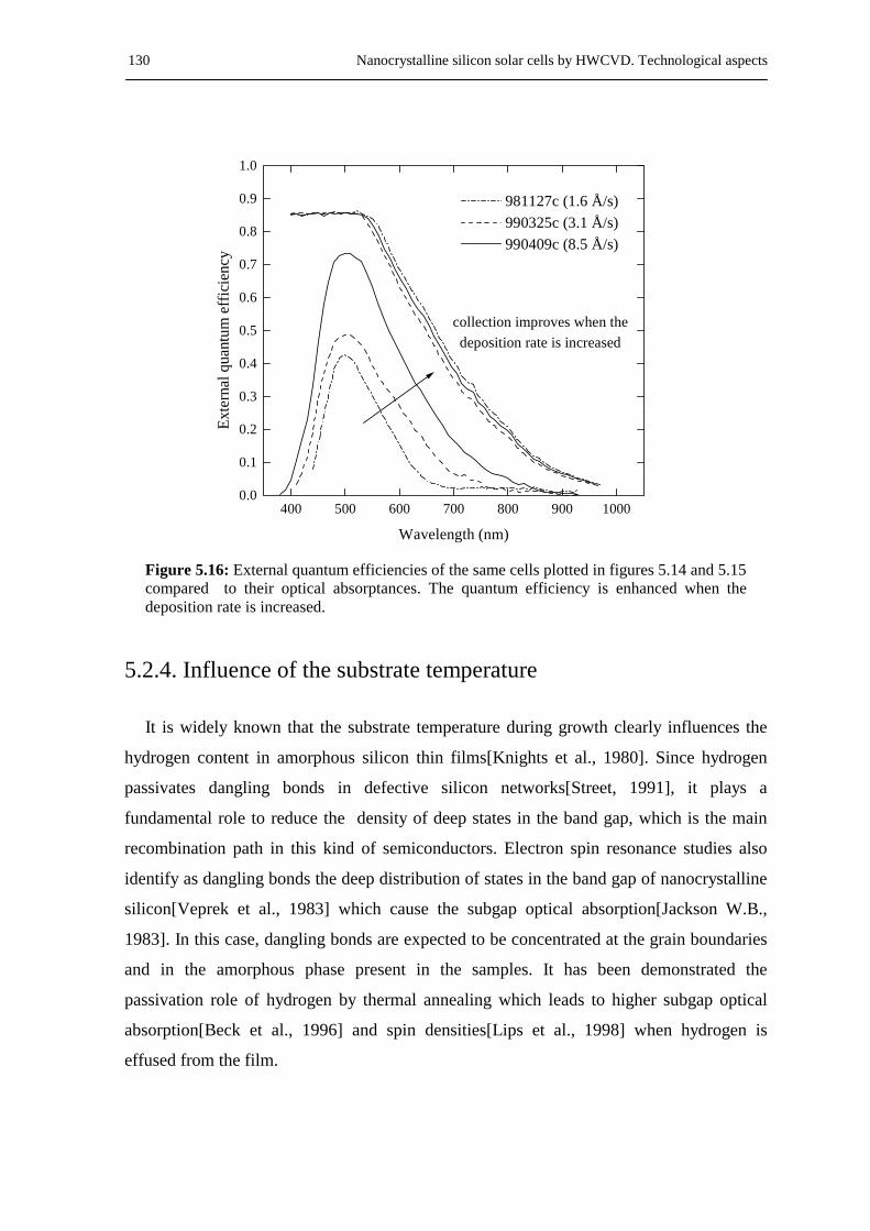
130 Nanocrystalline silicon solar cells by HWCVD. Technological aspects
400 500 600 700 800 900 10000.0
0.1
0.2
0.3
0.4
0.5
0.6
0.7
0.8
0.9
1.0
collection improves when thedeposition rate is increased
981127c (1.6 Å/s) 990325c (3.1 Å/s) 990409c (8.5 Å/s)
Wavelength (nm)
Exte
rnal
qua
ntum
effi
cien
cy
Figure 5.16: External quantum efficiencies of the same cells plotted in figures 5.14 and 5.15 compared to their optical absorptances. The quantum efficiency is enhanced when the deposition rate is increased.
5.2.4. Influence of the substrate temperature
It is widely known that the substrate temperature during growth clearly influences the
hydrogen content in amorphous silicon thin films[Knights et al., 1980]. Since hydrogen
passivates dangling bonds in defective silicon networks[Street, 1991], it plays a
fundamental role to reduce the density of deep states in the band gap, which is the main
recombination path in this kind of semiconductors. Electron spin resonance studies also
identify as dangling bonds the deep distribution of states in the band gap of nanocrystalline
silicon[Veprek et al., 1983] which cause the subgap optical absorption[Jackson W.B.,
1983]. In this case, dangling bonds are expected to be concentrated at the grain boundaries
and in the amorphous phase present in the samples. It has been demonstrated the
passivation role of hydrogen by thermal annealing which leads to higher subgap optical
absorption[Beck et al., 1996] and spin densities[Lips et al., 1998] when hydrogen is
effused from the film.
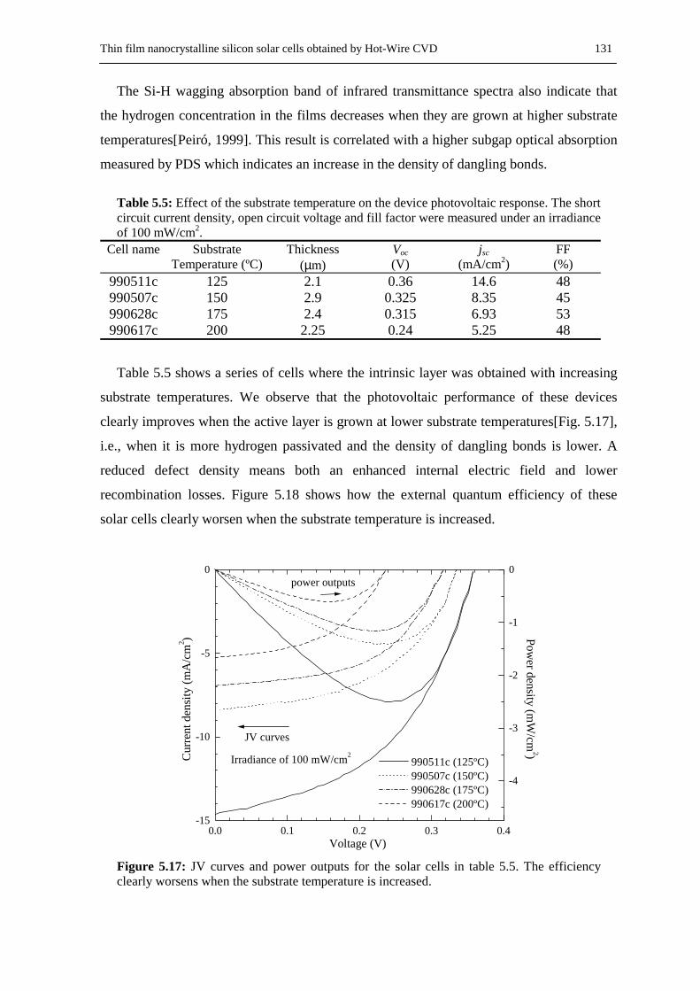
Thin film nanocrystalline silicon solar cells obtained by Hot-Wire CVD 131
The Si-H wagging absorption band of infrared transmittance spectra also indicate that
the hydrogen concentration in the films decreases when they are grown at higher substrate
temperatures[Peiró, 1999]. This result is correlated with a higher subgap optical absorption
measured by PDS which indicates an increase in the density of dangling bonds.
Table 5.5: Effect of the substrate temperature on the device photovoltaic response. The short circuit current density, open circuit voltage and fill factor were measured under an irradiance of 100 mW/cm2.
Cell name Substrate Temperature (ºC)
Thickness (µm)
Voc (V)
jsc (mA/cm2)
FF (%)
990511c 125 2.1 0.36 14.6 48 990507c 150 2.9 0.325 8.35 45 990628c 175 2.4 0.315 6.93 53 990617c 200 2.25 0.24 5.25 48
Table 5.5 shows a series of cells where the intrinsic layer was obtained with increasing
substrate temperatures. We observe that the photovoltaic performance of these devices
clearly improves when the active layer is grown at lower substrate temperatures[Fig. 5.17],
i.e., when it is more hydrogen passivated and the density of dangling bonds is lower. A
reduced defect density means both an enhanced internal electric field and lower
recombination losses. Figure 5.18 shows how the external quantum efficiency of these
solar cells clearly worsen when the substrate temperature is increased.
0.0 0.1 0.2 0.3 0.4-15
-10
-5
0
Power density (m
W/cm
2)Cur
rent
den
sity
(mA
/cm
2 )
Voltage (V)
-4
-3
-2
-1
0
Irradiance of 100 mW/cm2 990511c (125ºC) 990507c (150ºC) 990628c (175ºC) 990617c (200ºC)
power outputs
JV curves
Figure 5.17: JV curves and power outputs for the solar cells in table 5.5. The efficiency clearly worsens when the substrate temperature is increased.
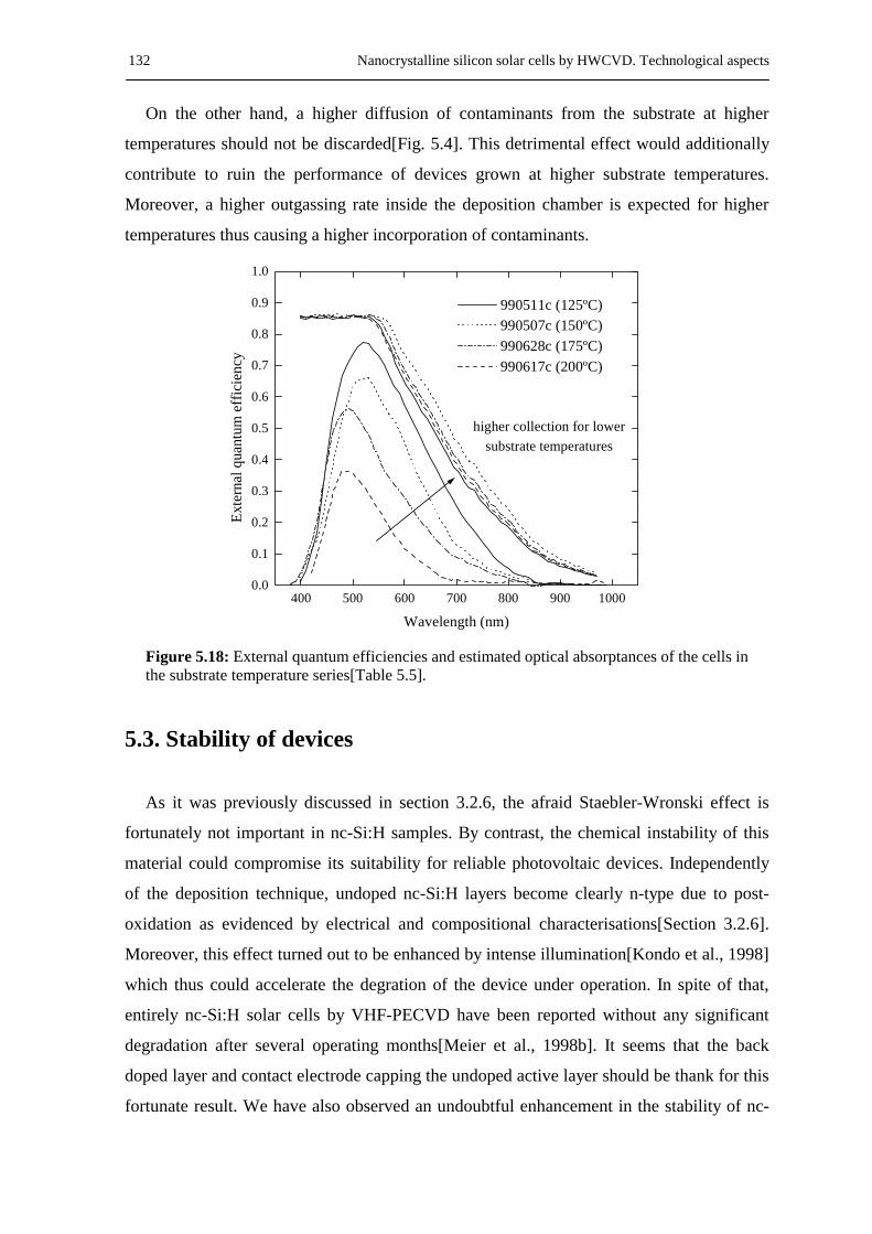
132 Nanocrystalline silicon solar cells by HWCVD. Technological aspects
On the other hand, a higher diffusion of contaminants from the substrate at higher
temperatures should not be discarded[Fig. 5.4]. This detrimental effect would additionally
contribute to ruin the performance of devices grown at higher substrate temperatures.
Moreover, a higher outgassing rate inside the deposition chamber is expected for higher
temperatures thus causing a higher incorporation of contaminants.
400 500 600 700 800 900 10000.0
0.1
0.2
0.3
0.4
0.5
0.6
0.7
0.8
0.9
1.0
higher collection for lowersubstrate temperatures
990511c (125ºC) 990507c (150ºC) 990628c (175ºC) 990617c (200ºC)
Wavelength (nm)
Exte
rnal
qua
ntum
eff
icie
ncy
Figure 5.18: External quantum efficiencies and estimated optical absorptances of the cells in the substrate temperature series[Table 5.5].
5.3. Stability of devices
As it was previously discussed in section 3.2.6, the afraid Staebler-Wronski effect is
fortunately not important in nc-Si:H samples. By contrast, the chemical instability of this
material could compromise its suitability for reliable photovoltaic devices. Independently
of the deposition technique, undoped nc-Si:H layers become clearly n-type due to post-
oxidation as evidenced by electrical and compositional characterisations[Section 3.2.6].
Moreover, this effect turned out to be enhanced by intense illumination[Kondo et al., 1998]
which thus could accelerate the degration of the device under operation. In spite of that,
entirely nc-Si:H solar cells by VHF-PECVD have been reported without any significant
degradation after several operating months[Meier et al., 1998b]. It seems that the back
doped layer and contact electrode capping the undoped active layer should be thank for this
fortunate result. We have also observed an undoubtful enhancement in the stability of nc-
Thin film nanocrystalline silicon solar cells obtained by Hot-Wire CVD 133
Si:H p-i-n solar cells by HWCVD by increasing the thickness of the n-doped layer[Fig.
5.19]. However, to date we can not ensure reliable long-term stabilities without
encapsulating the device. Besides, too thick doped layers could lead to a high parasitic
series resistance. Nevertheless, this problem could be not so dramatic as it seemed at first
sight. Several studies point to indeed thin (~10 nm) a-Si:H layers by PECVD as efficient
capping layers to prevent post-oxidation[Kondo et al., 1998]. However, a-Si:H by
HWCVD seems to be less efficient as a barrier to oxygen diffusion[Brühne et al., 2000].
Actually, the much lower ion bombardment in HWCVD processes compared to PECVD
ones, could lead to lower density materials which are thus more permeable to
contaminants. Probably this is one of the reasons why the group at the Debye Institute
grows both doped layers in their nc-Si:H p-i-n solar cells by PECVD instead of
HWCVD[Schropp et al., 1999]. Anyway, the deposition of a thin n-doped a-Si:H layer by
PECVD to encapsulate the entirely nc-Si:H solar cell obtained by HWCVD would not be a
dramatic drawback.
0.01 0.1 1 100.0
0.1
0.2
0.3
0.4
0.5
0.6
0.7
0.8
0.9
1.0
n-do
ped
laye
r thi
ckne
ss
991026c (200 nm) 990511c (100 nm) 990518c ( 30 nm)
Temperature = 30 ± 4 ºC
Irradiance = 100 mW / cm2
Exposure time (hours)
Nor
mal
ised
effic
ienc
y
Figure 5.19: Normalised efficiency of devices under light soaking. Steadily increasing stabilities are achieved by increasing the thickness of the n-doped layer which seems to cap the undoped active layer.

134 Nanocrystalline silicon solar cells by HWCVD. Technological aspects
Thin film nanocrystalline silicon solar cells obtained by Hot-Wire CVD 135
Conclusions 1. Thin film crystalline silicon solar cells have recently arisen as a very promising
alternative to the worn out amorphous silicon or the save but costly wafer technologies.
As the ratio of the drift length to the active layer thickness becomes the factor
determining the collection efficiency in thin film p-i-n structures, materials of lower
quality could be used. Therefore, microcrystalline and nanocrystalline silicon emerge as
exciting new materials with potentially higher improvement perspectives than other
traditional photovoltaic materials. In addition, this kind of small-grain silicon films can
be grown at moderate temperatures allowing the use of low cost foreign substrates such
as glass or even transparent polymer foils.
2. Among the different deposition techniques to obtain thin film hydrogenated
nanocrystalline silicon, the Hot-Wire Chemical Vapour Deposition has allowed the
highest deposition rates ever reported to date. Deposition rates in the range of several
tens of Å/s could be easily achieved maintaining reasonably good microstructural
properties over large areas. Furthermore, a HWCVD set-up is much easier to handle
and the implementation and upkeep costs are much lower than in a PECVD one.
However, multichamber set-ups are required in order to grow the undoped active layer
of p-i-n structures in a separate chamber to avoid cross-contamination.
3. The optimised hydrogenated nanocrystalline silicon layers by Hot-Wire CVD with high
crystalline fractions (>90%) showed an optical absorption coefficient significantly
higher than that of single crystal silicon. This enhanced optical absorption could not be
fully explained by the amorphous phase in the samples but elastic light scattering
mechanisms should be considered. Higher process pressures (>10-2 mbar) enhance the
columnar growth along the [220] crystalline direction, as observed by X-ray diffraction
and Scanning Electron Microscopy. This microstructure leads to highly textured film
surfaces with root mean square roughness in the range of a few per cent (~2%) of the
136 Conclusions
film thickness. The optical absorption enhancement in the near infrared could be
quantified in around a factor 2 for typical samples, which certainly causes an
advantageous increase in photogeneration.
4. Several electrical characterisations evidence an undesired as grown n-type character in
undoped nanocrystalline silicon samples obtained at low deposition rates (~2 Å/s). The
dark conductivity activation energy is far from midgap and the sign of the thermopower
indicates that the electronic transport is certainly due to free electrons in the conduction
band. In addition, very low p-type doping levels (solid phase B/Si ratio ~10-4 ) lead to
higher activation energies as well as lower room temperature dark conductivities. A
misleading increase in the Steady State Photoconductivity µτ-product is observed for
the less intrinsic samples. This effect is definitely not due to better transport properties
but to a change in the thermal occupation of recombination centres which results in a
longer lifetime for the majority carriers. The lifetime of minority carriers, which
actually limits the collection efficiency in photovoltaic devices, results undoubtedly
degrade in the less intrinsic samples.
5. By increasing the deposition rate over 5 Å/s, dark conductivity activation energies
around midgap were obtained. At one time, the density of charged centres in the gap
could be lowered from 1017 to 1016 cm-3, as determined from the voltage dependence of
the depletion capacitance of Schottky structures. These results could be explained by
the undesired incorporation of contaminants which could be attributed either to gas
phase impurities or to metallic components evaporated from the wire. Actually, several
shallow donor levels which could be attributed to oxygen (EC-ED≤0.14 eV) and cooper
(EC-ED≤0.185 eV) were resolved by Deep Level Transient Spectroscopy in our
samples. In any case, the concentration of contaminants incorporated into the film
would be inversely proportional to the deposition rate.
Thin film nanocrystalline silicon solar cells obtained by Hot-Wire CVD 137
6. Fortunately, the Staebler-Wronski effect does not play an important role in the stability
of nanocrystalline silicon by Hot-Wire CVD. However, a relative chemical instability
leading to an increased n-type character is observed for samples exposed to air for a
long time. A significant post-oxidation through the surface of the nanocrystalline
silicon films seems to be the reason of such instability. Besides, this post-oxidation is
somehow accelerated under high irradiances when photons are able to break weak
bonds thus favouring oxidation.
7. The front electrode selected for our superstrate solar cells was aluminium-doped zinc
oxide (AZO) on account of its excellent chemical stability against atomic hydrogen. On
the contrary, fluorine-doped tin oxide or tin-doped indium oxide do not withstand the
strongly reducing ambient during Hot-Wire processes. The AZO coatings were
obtained by magnetron sputtering from a ceramic target in the load-lock chamber. The
optimised front electrodes presented sheet resistances around 10 Ω/! and optical
transmittances over 85% in the wavelength range of interest. These values are similar to
the best reported in the literature. However, the relatively high substrate temperatures
required to obtain these optimised films (>300ºC) prevent them from being
incorporated as top TCO on low temperature nc-Si:H solar cells.
8. Our preliminary solar cells with p-i-n structure point to the screening of the internal
electric field within the active layer as the main limiting factor in the photovoltaic
conversion. Lower filament temperatures and faster deposition rates allowed a very
significant improvement in the performance of the solar cells. This result fully agrees
with the enhanced intrinsic character of the samples obtained under these cleaner
deposition conditions. To date, our best solar cell showed a 2.5% photovoltaic
conversion efficiency. It was entirely obtained by Hot-Wire CVD on AZO-coated glass
at an indeed low substrate temperature of 150ºC. The undoped active layer 2.4 µm thick
was grown at a high deposition rate of 15 Å/s, thus the process time was less than 30
minutes. On account of the preliminary character of the work, neither textured front
electrodes nor back reflectors were incorporated in the solar cell design. Besides, since
138 Conclusions
the p-layer was certainly too thick (~500 Å), just optical losses severely limited the
maximum expected efficiency. 9. From optical calculations, we estimate that our current devices would present short
circuit currents around 20 mA/cm2 if they incorporated light confinement strategies.
Considering the open circuit voltage and fill factor already obtained, this would result in
conversion efficiencies over 4%. In the future, the optimisation of a low temperature
top TCO, most probably ITO, will allow to incorporate back reflectors in our structures.
Besides, inverted n-i-p solar cells illuminated from the top side will be also tested.
These structures would benefit from the enhanced quality of the material at the top
interface with respect to the initial stages of growth.
Thin film nanocrystalline silicon solar cells obtained by Hot-Wire CVD 139
References Abelès F., Advanced optical techniques, A.C.S. van Heel, Amsterdam, 145 (1967). Asensi J.M., Ph.D.Thesis, University of Barcelona (1994). Asensi J.M., Merten J., Voz C., Andreu J., Journal of Applied Physics, 85, 5, 2939-2951 (1999). Bai Y., Ford D.H., Rand J.A., Proc. 14th European Photovoltaic Solar Energy Conference, 999 (1997). Beck N., Meier J., Fric J., Remes Z., Poruba A. Flückiger R., Pohl J., Shah A., Vanecek M., Journal of Non-Crystalline Solids, 198-200, 903-906 (1996). Beck N., Wyrsch N., Hof C., Shah A., J. Appl. Phys., 79, 9361-9367 (1996b). Beneking C., Rech B., Wieder S., Kluth O., Wagner H., Frammelsberger W., Geyer R., Lechner P., Rübel H., Schade H., Thin Solid Films, 351, 241-246 (1999). Bennet H.E., Porteus J.O., J. Opt. Soc. Am. A, 51, 1234 (1961). Bergmann, R.B., Applied Physics A, 69, 187-194 (1999). Brüggemann R., Main C., Physical Review B, Volume 57, Number 24, R15 080-083 (1998). Brühne K., Klein S., Schubert M.B., 16th European Photovoltaic Solar Energy Conference, Glasgow, in press (2000). Burstein E., Physical Review B, 25, 7826 (1982). Carlson D.E., Williams B.F., U.S. Patent No. 4442310, April 10, 1984. Chiang K.L., Dell’Oca C.J., Schwettmann, J. Electrochem. Soc., 126, 2267-2269 (1979). Cifre J., Bertomeu J., Puigdollers J., Polo M.C., Andreu J., Applied Physics A, 59, 645 (1994). Crandall R.S., J. Appl. Phys., 54, 7176 (1983). Curry R., Photovoltaic Insiders’ Report, 17, 1 (1998). Curtins H., Favre M., Amorphous Silicon and Related Materials, World Scientific Publishing Company, 329-363 (1988).
140 References
Delgado J.C., Andreu J., Sardin G., Morenza J.L., Thin Solid Films, 191, 283-295 (1990). Diehl F., Schröder B., Oechsner H., Journal of Applied Physics, 84, 6, 3416-3418 (1998). Dusane R.O., Dusane S.R., Bhide V.G., Kshirsagar S.T., Appl. Phys. Lett., 63, 2201-2203 (1993). Flückiger R.S., Ph.D.Thesis, University of Neuchâtel (1995). Goerlitzer M., Beck N., Torres P., Meier J., Wyrsch N., Shah A., J. Appl. Phys. 80 (9), 5111-5115 (1996). Goerlitzer M., Torres P., Beck N., Wyrsch N., Keppner H., Pohl J., Shah A., Journal of Non-Crystalline Solids, 227-230, 996-1000 (1998). Goerlitzer M., Torres P., Droz C., Shah A., Solar Energy Materials and Solar Cells, 60, 195-200 (2000). Goetz M., Vaucher S., Tscharner R., Shah A., Proc. 12th EC Photovoltaic Science Engineering Conf., Amsterdam, 1229-1232 (1994). Gordon R., Proscia J., Ellis F.B., Delahoy A.E., Solar Energy Mater., 18, 263-281 (1989). Green M.A., Prog. Photovolt. Res. Appl., 2, 87-94 (1994). Guillet J., Ph.D.Thesis, INPG Grenoble (1998). Hack M., Shur M., J. Appl. Phys. 58, 997 (1985). Hagedorn G., Kumulierter Energieaufwand von Photovoltaik- und Winddraftanlagen, IFE Schriftenreiche Heft 25, Ed. Lehrstuhl f. Energiewirtschaft und Kraftwerkstechnik, TU München (1992). Hof C., Ph.D. Thesis, Institut de Microtechnique, Université de Neuchâtel (1999). Hubin J., Shah A.V., Philos. Mag. B, 72(6), 589-599 (1995). Isomura M., Kinoshita T., Hishikawa Y., Tsuda S., Appl. Phys. Lett., 65(18), 2329-2331 (1994). Jackson W.B., Amer N.M., Boccara A.C., Fournier D., Appl. Optics, 20, 1333 (1981). Jackson W.B., Amer N.M., Phys. Rev. B, 25, 5559 (1982). Jackson W.B., Johnson N.M., Biegelsen D.K., Appl. Phys. Lett., 43(2), 195-197 (1983). Jackson W.B., Phys. Rev. B, 38, 3595 (1988).
Thin film nanocrystalline silicon solar cells obtained by Hot-Wire CVD 141
Jäger S., Szyszka B., Szczyrbowski J., Bräuer G., Surface and Coatings Technology, 98, 1304-1314 (1998). Jain V.K., Kulshreshtha A.P., Solar Energy Mater., 4, 151 (1981). Kalkan K., Fonash S.J., Materials Research Socienty Symp. Proc., 467, 319-324 (1997). Kamins T., Polycrystalline silicon for integrated circuit applications, Kluwer Academic Publishers, Norwell (1988). Keppner H., Meier J., Torres P., Fischer D. Shah A., Appl. Phys. A, 69, 169-177 (1999). Kim K.H., Park K.C., Ma D. Y., J. Appl. Phys., 81(12), 7764-7772 (1997). Kluth O., Löffl A., Wieder S., Beneking C., Appenzeller W., Houben L., Rech B., Wagner H., Hoffmann S., Waser R., Anna Selvan J.A., Keppner H., Proc. of the 26th IEEE Photovoltaics Specialists Conference, Anaheim CA (USA), 715-718 (1997). Knights J.C., Lucovsky G., CRC Critical Reviews in Solid State Materials Sciences, 21, 211 (1980). Kondo M., Nishimiya T., Saito K., Matsuda A., Journal of Non-Crystalline Solids, 227-230, 1031-1035 (1998). Kroll U., Meir J., Keppner H., Shah A., Littlewood S.D., Kelly I.E., Giannoulès P., J. Vac. Sci. Technol. A, 13, 2742-2746 (1995). Kroll U., Shah A., Keppner H., Meier J., Torres P., Fischer D., Solar Energy Materials and Solar Cells, 48, 343-350 (1997). Lips K., Kanschat P., Will D., Lerner C., Fuhs W., Journal of Non-Crystalline Solids, 227-230, 1021-1025 (1998). Lucovsky G., Wang C., Williams M.J., Chen Y.L., Maher D.M., Mater. Res. Soc. Symp., Proc. 283, 443 (1993). Mahan H., Reedy R.C., Iwaniczko E., Wang Q., Nelson B.P., Xu Y., Gallagher A.C., Branz H.M., Crandall R.S., Yang J., Guha S., Materials Research Society Symp. Proc., 507 (1998). Masuda A., J. Non-Cryst. Solids, 59-60, 767 (1983). Matsumura H., Jpn. J. Appl. Phys., 25, L949 (1986). Matsumura H., Materials Research Society Symp. Proc., 118, 43-48 (1988). Matsumura H., Jpn. J. Appl. Phys., 30, L1522 (1991).
142 References
Matsuyama T., Baba T., Takahama T., Tsuda S., Nishiwaki H., 13th European Photovoltaic Solar Energy Conference and Exhibition, Nice (1995). Matsuyama T., Terada N., Baba T., Sawada T., Tsuge S., Wakisaka K., Tsuda T., J. Non-Cryst. Solids, 198-200, 940 (1996). Meier J., Flückiger R., Keppner H., Shah A., Appl. Phys. Lett., Volume 65, 860 (1994). Meier J., Dubail S., Platz R., Torres P., Kroll U., Anna Selvan J.A., Vaucher N.P., Hof C., Fischer D., Keppner H., Flückiger R., Shah A., Shklover V., Ufert K.D., Solar Energy Materials and Solar Cells 49, 35-44 (1997). Meier J., Keppner H., Dubail S., Ziegler Y., Feitknecht L., Torres P., Hof Ch., Kroll U., Fischer D., Cuperus J., Anna Selvan J.A., Shah A., 2nd World Conf. on Photovoltaic Solar Energy Conversion, Vienna, Volume I, 375-379 (1998). Meier J., Dubail S., Cuperus J., Kroll U., Platz R., Torres P., Anna Selvan J.A., Pernet P., Beck N., Pellaton Vaucher N., Hof Ch., Fischer D., Keppner H., Shah A., Journal of Non-Crystalline Solids, 227-230, 1250-1256 (1998b). Meiling H., Schropp R.E.I., Appl. Phys. Lett., 70, 2681-2683 (1997). Meiling H., Schropp R.E.I., Appl. Phys. Lett., Vol. 74, No. 7, 1012-1014 (1999). Merten J., Ph.D.Thesis, University of Barcelona (1996). Merten J., Asensi J.M., Voz C., Shah A.V., Platz R., Andreu J., IEEE Transactions on Electron Devices, Vol. 45, No. 2, 423-429 (1998). Meyer W., Neldel H., Z. Tech. Phys. (Leipzig) 18, 588 (1937). Milford E., Renewable Energy World, Vol. 2, Nº 1, 80 (1999). Möller H.J., Semiconductors for Solar Cells, Artech House, Norwood (1993). Nelson B.P., Iwaniczko E., Schropp R.E.I., Mahan H., Molenbroek E., Salamon S., Crandall R.S., 12th International EC Photovoltaic Solar Energy Conference, 679-682 (1994). Niikura C., Brenot R., Vanderhaghen R., Poisant Y., Roca P., Bourée J.E., Kleider J.P., Longeaud C., 16th European Photovoltaic Solar Energy Conference and Exhibition, Glasgow, in press (2000). Palz W., Renewable Energy World, Vol. 3, Nº 2, 24-37 (2000). Pauli M., Doscher M., Salentiny G., Homberg F., Muller J., 11th EC Photovoltaic Solar Energy Conference, Montreux, 525 (1992).
Thin film nanocrystalline silicon solar cells obtained by Hot-Wire CVD 143
Papadopoulos P., Scholz S., Bauer S., Schröder B., Öchsner H., J. Non-Cryst. Solids, 164-166, 87-90 (1993). Peiró D., Bertomeu J., Voz C., Asensi J.M., Puigdollers J., Andreu J., 14th European Photovoltaic Solar Energy Conference, Barcelona, 1428 (1997). Peiró D., Ph.D.Thesis, University of Barcelona (1999). Peiró D., Bertomeu J., Voz C., Fonrodona M., Soler D., Andreu J., Materials Science and Engineering B, 60-70, 536-541 (2000). Pernet P., Goetz M., Niquille X., Fischer D., Shah A., Althaus H., Haller A., 2nd World Conf. on Photovoltaic Solar Energy Conversion, Vienna, Volume I, 976-979 (1998). Poruba A., Remes Z., Springer J., Vanecek M., Fejfar A., Kocka J., Meier J., Torres P., Shah P., 2nd World Conf. on Photovoltaic Solar Energy Conversion, Vienna, Volume I, 781-785 (1998). Puigdollers J., Cifre J., Polo M.C., Asensi J.M., Bertomeu J., Andreu J., Lloret A., Appl. Surf. Sci., 86, 600 (1995). Puigdollers J., Ph.D.Thesis, University of Barcelona (1995b). Puigdollers J., Dosev D., Orpella A., Voz C., Peiró D., Bertomeu J., Marsal L.F., Pallarés J., Andreu J., Alcubilla R., Materials Science and Engineering B, 69-70, 526-529 (2000). Rath J.K., Galetto M., Van der Werf C.H.M., Feenstra K., Meiling H., Van Cleef M.W.M., Schropp R.E.I., Technical Digest of the 9th International Photovoltaic Science and Engineering Conference, Miyazaki, 227 (1996) Rath J.K., Meiling H., Schropp R.E.I., Jpn. J. Appl. Phys., 36, 5436 (1997). Rath J.K., Meiling H., Schropp R.E.I., Solar Energy Materials and Solar Cells, 48, 269-277 (1998). Rath J.K., Schropp R.E.I., Materials Research Society Symp. Proc., 557, in press (1999). Rhoderick E.H., Metal-Semiconductor Contacts, Clarendon Oxford (1978). Ritter D., Weiser K., Optics Communications, Volume 57, 336-338 (1986). Rose A., Concepts in photoconductivity and allied problems, John Wiley & Sons, New York (1963). Ruff D., Mell H., Tóth L., Sieber I., Fuhs W., Journal of Non-Crystalline Solids, 227-230, 1011-1015 (1998).
144 References
Saito K., Sano M., Matuda K., Kondo T., Nishimoto T., Ogawa K., Kajita I., 2nd World Conf. on Photovoltaic Solar Energy Conversion, Vienna, Volume I, 351-354 (1998). Sauvain E., Ph.D. Thesis, Institut de Microtechnique, Université de Neuchâtel (1992). Shah A.V., Platz R., Keppner H., Solar Energy Materials and Solar Cells, 38, 501-520 (1995). Shah A., Sauvain E., Hubin J., Pipoz P., Hof C., Philosophical Magazine B, 75(6), 925-936 (1997). Shi Z., Green M.A., Prog. Photovolt. Res. Appl., 6, 247-257 (1998). Schropp R.E.I., Zeman M., Amorphous and microcrystalline silicon solar cells, Kluwer Academic Publishers, Dordrecht (1998). Schropp R.E.I., Rath J.K., IEEE Transactions on Electron Devices, Vol. 46, No. 10, 2069-2071 (1999). Schubert M.B., Brüggemann R., Bilger G., Hierzenberger A., 2nd World Conf. On Photovoltaic Solar Energy Conversion, Vienna, Volume I, 834-837 (1998). Sopori B.L., Madjdpour J., Chen W., 2nd World Conf. on Photovoltaic Solar Energy Conversion, Vienna, Volume I, 156-159 (1998). Staebler D.L., Wronski C.R., Appl. Phys. Lett., Volume 31, 292 (1977). Starobinski L., Dus R., Vacuum, 46, 433 (1995). Stöger M., Breymesser A., Schlosser V., Ramadori M., Plunger V., Peiró D., Voz C., Bertomeu J., Nelhiebel M., Schattschneider P., Andreu J., Physica B, 273-274, 540-543 (1999). Street R.A., Hydrogenated Amorphous Silicon, Cambridge University Press, Cambridge (1991). Strese D., Die Ludwig-Bölkow-Studie: Solarstrom wird retabel in: Bild der Wissenschaft 7, 49-56 (1998). Swanepoel R., J. Phys. E:Sci. Instrum., Volume 16, 1214-1222 (1983). Sze S.M., Physics of semiconductor devices, Wiley & Sons, New York (1985). Tarui H., Matsuyama T., Okamoto S., Dohjoh H., Hishikawa Y., Nakamura N., Tsuda S., Nakano S., Ohnishi M., Kuwano Y., Jpn. J. Appl. Phys., 28, 2436 (1989).
Thin film nanocrystalline silicon solar cells obtained by Hot-Wire CVD 145
Tsai C.C., Thompson R., Doland C., Ponce F.A., Anderson G.B., Wacker B., Materials Research Society Symp. Proc. 118, 49-54 (1988). Torres P., Meier J., Flückiger, Kroll U., Anna Selvan J.A., Keppner H., Shah A., Appl. Phys. Lett., 69, 1373-1375 (1996). Torres P., Ph.D. Thesis, Institut de Microtechnique, Université de Neuchâtel (1998). Tsai C.C., Proc. of the Int. Workshop on Amorphous Semiconductors, World Scientific Publishing Co., 113 (1987). Twidell J., Renewable Energy World, Vol. 2, Nº 1, 45-49 (1999). Vanecek M., Kocka J., Stuchlik J., Kozisek Z., Stika O., Triska A., Solar Energy Materials, 8, 411 (1983). Varadi P., Renewable Energy World, Vol. 1, Nº 3, 12-19 (1998). Veprek S., Iqbal Z., Kühne R.O., Capezzuto P., Sarott F.A., Gimzewski J.K., J. Phys. C Solid State Phys., 16, 6241 (1983). Vetterl O., Hapke P., Kluth O., Lambertz A., Wieder S., Rech B., Finger F., Wagner H., Solid State Phenom., 67-68, 101 (1999). Voz C., Peiró D., Bertomeu J., Soler D., Fonrodona M., Andreu J., Materials Science and Engineering B, 69-70, 278-283 (2000). Voz C., Peiró D., Fonrodona M., Soler D., Bertomeu J., Andreu J., Solar Energy Materials & Solar Cells, 63, 237-246 (2000b). Voz C., Fonrodona M., Soler D., Peiró D., Asensi J.M., Bertomeu J., Andreu J., 16th European Photovoltaic Solar Energy Conference, Glasgow, in press (2000c). Wallinga J., Arnoldbik W.M., Vredenberg A.M., Schropp R.E.I., van der Weg W.F., J. Phys. Chem. B, 102, 6219-6224 (1998). Wang X., Bar-Yam Y., Adler D., Joannopoulos J.D., Phys. Rev. B, 38, 1601 (1988). Wanka H.N., Lotter E., Schubert M.B., Materials Research Society. Symp. Proc., 336, 657-662 (1994). Wanka H.N., Zedlitz R., Heintze M., Schubert M.B., 13th European Photovoltaic Solar Energy Conference, Nice, Volume II, 1753-1756 (1995). Ward L., The optical constants of bulk materials and films, IOP Publishers 2nd Edition, Bristol, 246 (1994).
146 References
Wenham S.R., Green M.A., Watt M.E., Applied Photovoltaics, Bridge Printery, Sydney (1994). Wiesmann H., Ghosh A.K., McMahon T., Strongin M., J. Appl. Phys., 50, 3752 (1979). Wiesmann H., Method of producing hydrogenated amorphous silicon film, U.S. Patent 4237150, (1980). Yamamoto K., Yoshimi M., Suzuki T., Tawada Y., Okamoto T., Nakajima A., 2nd World Conf. on Photovoltaic Solar Energy Conversion, Vienna, Volume II, 1284-1289 (1998).

Thin film nanocrystalline silicon solar cells obtained by Hot-Wire CVD 147
Acronym list A absorptance α optical absorption coefficient AM1.5 Air Mass 1.5 a-Si:H hydrogenated amorphous silicon AZO aluminium-doped zinc oxide χ collection efficiency C depletion capacitance Cat-CVD Catalytic CVD c-Si monocrystalline silicon CVD Chemical Vapour Deposition d layer thickness E electric field strength, energy level e elementary charge Ea dark conductivity activation energy Eg optical band gap EMN Meyer-Neldel rule activation energy εs dielectric permitivity of silicon FF fill factor FTO fluorine-doped tin oxide G generation rate γ SSPC gamma exponent, linear coefficient of the band gap thermal dependence η conversion efficiency H Haze ratio HWCVD Hot-Wire CVD I irradiance ITO tin-doped indium oxide j current density kB Boltzmann’s constant λ wavelength Ldiff diffusion length Ldrift drift length Lscreen screening length µc-Si:H hydrogenated microcrystalline silicon MFC mass flow controller µn electron mobility µp hole mobility µτph steady state photoconductivity µτ-product n density of electrons, refractive index, diode ideality factor NC effective density of charged centres, conduction band effective density of states
148 Acronym list
nc-Si:H hydrogenated nanoocrystalline silicon ND density of donor states Ndb density of dangling bonds NV valence band effective density of states p density of holes P power density, pressure PDS Photothermal Deflection Spectroscopy PECVD Plasma-Enhanced CVD PID proportional-integral-derivative temperature control p-Si polycrystalline silicon PV photovoltaic QE quantum efficiency R reflectance, resistance, recombination rate ρ space charge density, resistivity rd deposition rate RF radio frequency σ dark conductivity, capture cross-section SEM Scanning Electron Microscopy SIMS Secondary Ion Mass Spectroscopy σo dark conductivity prefactor σoo Meyer-Neldel rule prefactor σph steady state photoconductivity σr root mean square surface roughness sccm standard cubic centimetre SR spectral response SSPC Steady State Photoconductivity T transmittance, absolute temperature TCO transparent conductive oxide TFT thin film transistor UHV ultra-high vacuum Vbi built-in voltage VC voltage collection Vd Schottky barrier VHF-PECVD Very High Frequency PECVD w width of the depletion region XC crystalline fraction XPS X-ray photoelectron spectroscopy XRD X-ray diffraction
Thin film nanocrystalline silicon solar cells obtained by Hot-Wire CVD 149
Figure list Figure 1.1: Expected global warming due to the Greenhouse effect during the next century computed at the Max Planck Institute for Meteorology a) for an unabated increase in carbon dioxide emissions and b) with accelerated policies promoting renewable energy sources in order to reduce carbon dioxide emissions[www.dkrz.de]. Figure 1.2: Prediction of averaged component costs in PV systems and price reduction over time[acre.murdoch.edu.au]. Thin film technologies must allow to reduce singnificantly the costs of module manufacturing. Figure 1.3: Worldwide PV shipments production[Curry, 1998]. The major manufacturers of solar panels are Solarex and USSC in the USA, Sanyo, Canon and Kyocera in Japan and BP Solar and Siemens Solar in Europe. There are many other smaller manufacturers. Figure 1.4: Percentage of costs for the production of crystalline-Si photovoltaic modules based on wafer technology (450 µm). Figure 1.5: Typical thin film solar cell structure. Glass is used as a carrier for the front electrode and the active device, in this case a p-i-n structure. Contacts are usually thin metallic films thermally evaporated in high vacuum. Figure 1.6: Relative thicknesses of conventional bulk silicon and thin film crystalline silicon solar cells compared to the thickness of a human hair. Figure 1.7: Processing temperatures and thicknesses of absorber materials for several photovoltaic technologies[Beneking et al., 1999]. Figure 1.8: Deposition time as a function of the deposition rate. The filled region represents the field of interest for photovoltaic applications[Keppner et al., 1999]. Figure 2.1: Picture of the multichamber HWCVD set-up at University of Barcelona. The three inline UHV chambers were fabricated at the Vacuum Unit of the Scientific-Technical Service of University of Barcelona. Figure 2.2: Boron profile by SIMS in the active layer of a p-i-n structure obtained in a sole chamber compared to the case of a p-i-n solar cell where the intrinsic layer was grown in a different chamber. Figure 2.3: Schematic of one of the HWCVD chambers showing the inner arrangement of its accessories. Figure 2.4: Detailed schematics of the multichamber HWCVD set-up and the pumping system [Peiró, 1999]. Figure 2.5: Diagram of the gas panels[Peiró, 1999]. Microflows of diborane and phosphine are added to the base silane-hydrogen gas mixture in the feedgas to p- and n-type dope respectively. Nitrogen is the purging gas. Figure 2.6: Experimental set-up used to perform the high-impedance dark conductivity measurements in vacuum. Figure 2.7: Geometry of the coplanar electrodes on the samples. They are obtained by thermal evaporation of aluminium in high vacuum. The distance l between them is 1mm while their width w is 10mm. Since l~103d for typical film thickness’, we neglect edge effects in the current lines to calculate the conductivity. Figure 2.8: Thermal dependence of the dark conductivity for an undoped nc-Si:H sample obtained by HWCVD. Its high activation energy indicates the intrinsic character of the sample. Figure 2.9: Experimental set-up for the steady state photoconductivity measurement. The monochromatic incident photon flux Φ is determined with a calibrated photodetector. The absorption of these photons with energies higher than the band gap mainly result in the generation of electron-hole pairs.
150 Figure list
Figure 2.10: Mean steady state photoconductivity and SSPC µτ-product as a function of the mean generation rate for a typical undoped nc-Si:H sample obtained by HWCVD. A sublinear behaviour <σ ph>~<G>γ with γ =0.85 is observed because µτ ph significantly depends on the generation rate. Figure 2.11: The transverse PDS set-up in our laboratory. The experiment is automatised with a personal computer. The deflection detector consists of two adjacent reverse biased photodetectors. Figure 2.12: Deflection of the probe beam by the mirage effect. The thickness of the He-Ne laser probe beam is considered infinitesimal (dz). Figure 2.13: Optical absorption coefficient of typical hydrogenated amorphous and nanocrystalline silicon thin films measured with the PDS system in our laboratory. They are compared to the tabulated optical absorption of crystalline silicon[Möller, 1993]. Figure 2.14: Experimental set-up for measuring the JV curve of solar cells in the dark or under varied irradiances. Note the four quadrant voltage source and current-voltage converter to ensure enough sensitivity without the loading effects with high shunt resistances. Figure 2.15: Typical JV curve under illumination of a p-i-n solar cell. It generates electrical power in the 4th quadrant (power dissipated P=V×J<0). The fill factor FF corresponds to the ratio of the area delimited by jmp and Vmp in the maximum power point with respect to the area determined by jsc and Voc. Figure 2.16: The spectral response measurement set-up. Bias light from the halogen lamp can be superimposed to the monochromatic probe beam arriving through the optic fiber. The experiment is automatised with a personal computer. Figure 2.17: Optical absortance in the whole device and only in the active layer compared to the short circuit external quantum efficiency of a 2.1µm thick p-i-n nc-Si:H solar cell obtained by HWCVD[Table 2.2]. Figure 2.18: Short circuit internal quantum efficiency (collection efficiency) of the same solar cell in figure 2.17. It is also plotted the penetration length as a function of the wavelength. Figure 2.19: Structures used for the standard depletion capacitance-reverse voltage measurement. Either heavily p-doped nc-Si:H or ZnO:Al allow to obtain rectifying contacts with undoped-nc-Si:H. The evaporated chromium back contact turned out to be quasi ohmic as evidenced in Cr/undoped nc-Si:H/Cr sandwich structures which did not show any rectifying behaviour. Figure 2.20: Voltage dependence of the depletion capacitance of a ZnO:Al/undoped nc-Si:H pseudo Schottky contact. The nice linear behaviour, together with the slight differences (<10%) between the depletion region widths obtained either from equation 2.21 or 2.25, indicate that the assumptions of the simplified model are fulfilled. The inset current density-voltage characteristic shows a satisfactory rectifying behaviour. Figure 2.21: Simulation results compared to the analytical model within the one-sided abrupt juction approximation for an uniform density of charged centres NC of 2×1017cm-3. The relatively rough abrupt-junction approximation satisfactorily reproduces the electric field and voltage profiles for x≤w. Figure 3.1: System formed by an absorbing smooth thin film on an infinite substrate. The extinction coefficient k in the complex refractive index n of the film relates to the optical absorption coefficient by λπα k4= . A fraction R of the incident power density I is reflected whereas T is transmitted. Hence, A=1-T-R is the fraction absorbed within the film. Figure 3.2: Simplified model to evaluate the optical absorptance A within the film. The reflection at the film-substrate interface of the attenuated irradiance is not considered while r is the Fresnel reflection coefficient at the air-film interface. Figure 3.3: Optical absorption coefficient calculated from the sole absorptance spectrum and improved calculation considering also the transmittance spectrum for a HWCVD nanocrystalline silicon layer 2 µm thick.
Thin film nanocrystalline silicon solar cells obtained by Hot-Wire CVD 151
Figure 3.4: Effective optical absorption coefficient, according to the effective media model, for a nc-Si:H sample with a 90% of crystalline fraction. The amorphous phase, with an optical gap of 1.8 eV, was considered of poor quality: defect density of 1018 cm-3 and Urbach front of 90 meV. Figure 3.5: Optical absorption coefficients measured by PDS for the HWCVD nc-Si:H samples in table 3.1. It is also shown the effective optical absorption coefficient expected for a 90% crystalline fraction. The corresponding ratios are also plotted as a measure of the optical absorption enhancement. Figure 3.6: Optical absorptances expected for 2 µm thick films with the optical absorption coefficient spectra in figure 3.5. Note the higher absorptance in the near infrared obtained when αHP was used for the calculation. Figure 3.7: Optical absorptance of a 2 µm thick HWCVD nc-Si:H sample (HP in table 3.1) compared with that of a 0.4 µm thick PECVD a-Si:H sample. The relatively high a-Si:H band gap causes important optical losses when the solar AM1.5 spectrum is considered. Figure 3.8: Calculated optical absorptances in the active layer for the device structures in table 3.2. The measured external quantum efficiency of the 990323c solar cell[Section 2.3.2] is also shown for comparison (dashed line). Note the additional losses due to either interface or bulk recombination depending on the wavelength range. Figure 3.9: Experiment to easily detect elastic light scattering. a) When the detector is placed just behind the substrate, all the transmitted irradiance contributes to the measured spectrum (integrated transmittance). b) If it is placed away from the substrate and its aperture φ is reduced with a mask, only the transmitted irradiance in a direction near to that of the incident beam will reach the detector (specular transmittance). Figure 3.10: Integrated and specular transmittances for a 1.5 µm thick HWCVD nc-Si:H silicon sample. The specular transmittance was measured by placing the detector 2 cm away from the sample and reducing its aperture to 1 cm (deviation of 14º from the incident direction). With this geometry, the measured Haze ratio was around 10% over the whole spectrum. Figure 3.11: Experiment to evaluate the rms roughness of a nc-Si:H film according to equation 3.11. The smooth wafer does not present diffuse reflection. Hence, specular reflectance equals total reflectance in that case. Figure 3.12: Scanning Electron Microscopy view of a nc-Si:H sample. Note the columnar structure of the film (bulk scattering) and its as grown textured surface (surface scattering). Figure 3.13: Determination of the rms roughness of the HWCVD nc-Si:H samples from reflectance measurements. The angle of incidence was 45º. Figure 3.14: Trajectory of a ray from the incident beam of light scattered at the rough surface of the film. Its effective optical path through the sample becomes d/cosθ. Figure 3.15: Expected optical absorption coefficient enhancement as a function of the scattered light distribution (Φ=Φocosnθ). For n=1.4 we obtain the factor 1.75 experimentally observed in our rough samples. Figure 3.16: Approximate and exact calculation of the dark conductivity of ideally intrinsic single crystal silicon as a function of the temperature. Figure 3.17: Conventional Meyer-Neldel rule observed in different series of undoped nc-Si:H samples obtained by HWCVD[Table 3.4]. The thermal shrinking of the band gap does not fully explain the strong exponential behaviour. Figure 3.18: Room temperature dark conductivity and corresponding activation energies for a p-doping series of samples[Table 3.5]. An increase in the activation energy as well as a lower room temperature dark conductivity is observed for low p-doping levels. Figure 3.19: Effect of the deposition rate on the intrinsic character of undoped nc-Si:H samples[Table 3.4]. The dark conductivity activation energy increases with the deposition rate.
152 Figure list
Figure 3.20: Current density-voltage characteristics for both types of studied pseudo-Schottky contacts. Slight differences in the rectifying behaviours were observed which however do not influence the depletion capacitance-voltage experiment. Figure 3.21: Determination of the concentration of charged centres from the voltage dependence of the depletion capacitance for the pseudo-Schottky contacts in table 3.6. Figure 3.22: Steady state photoconductivity µτ-product as a function of the dark conductivity activation energy for several series of undoped nc-Si:H samples[Table 3.4]. The values of µτ ph are those obtained for a mean generation rate of 1019 cm-3 s-1[Section 2.2.2]. A misleading increase in µτ ph is observed for the less intrinsic samples. Figure 3.23: Calculated occupation functions of the dangling bond[Eq. 3.28] depending on the electron to hole densities ratio (bottom axis) or the relative Fermi-level shift from midgap(top axis). The slight dissymmetry is due to the factor 3 between the capture cross-sections of electrons and holes by neutral dangling bonds[Table 3.7]. Figure 3.24: Different µτ-products as a function of the parameter b (bottom axis) or the relative shift of the Fermi-level from midgap (top axis). For the calculation we have used µ n=10 cm2/Vs, µp=3 cm2/Vs and Ndb =1016 cm-3 which leads to µτ ph =10-7 cm2/V for midgap samples. Figure 3.25: An steady increase is observed in the photoconductivity of samples kept under high irradiances for a long time. The light soaking experiment was performed with 100mW/cm2 of white light. Hence, the Staebler-Wronski effect does not play an important role in the stability of nc-Si:H. Figure 3.26: Change in the dark conductivity and activation energy of a nc-Si:H sample obtained by HWCVD due to post-oxidation in air. A pronounced n-type character is observed after 45 days. Figure 3.27: Infrared transmittance spectra for two pieces of the same sample 24 hours after deposition either kept in the dark or light-soaked under 100mW/cm2 of white light. The as deposited transmittance is also shown for comparison. The pronounced overlapped bands at 1050 and 1140cm-1 corresponding to Si-O-Si stretching modes indicate a faster post-oxidation in the light soaked piece. Figure 4.1: Equivalent circuit of a photovoltaic device. For low mobility p-i-n structures a recombination term must be added to the typical single exponential model. In order to allow the more reasonable work with current densities, Rs and Rp are actually effective series and parallel resistances calculated as the product of the corresponding absolute values ℜ s and ℜ p and the active area of the device S, i.e., RS=Sℜ s and Rp=Sℜ p . Figure 4.2: Parameters to determine for each JV curve which are used for the VIM analysis. Figure 4.3: Determination of the voltage collection from linear fits to the JV curves around the short circuit point. Figure 4.4: Results from the VIM characterisation method for the same device before and after dry-etching the surrounding layers. Figure 4.5: VIM data for the 990409c HWCVD solar cell[Table 4.1]. The measured values can be perfectly fitted over irradiances varying more than four orders of magnitude. Figure 4.6: Results from the analytical description for an active layer thickness d of 2µm and a a dangling bond density Ndb of 1016cm-3. The built-in potential Vbi is 1V which considering a band gap of 1.2eV corresponds to doped layers with the typically obtained dark conductivity activation energies around 0.1eV. We have considered a dangling bond correlation energy Ueff =Vi of 0.3eV and Vp=Vn=0.35V. Note that Vbi=Vp+Vi+Vn. Figure 4.7: (a) Set of parameters determining the electric field profile as a function of the active layer thickness considering a dangling bond density of 1016 cm-3. (b) As a function of the dangling bond density considering an active layer thickness of 2 µm.
Thin film nanocrystalline silicon solar cells obtained by Hot-Wire CVD 153
Figure 4.8: (a) Short circuit collection efficiency as a function of the active layer thickness for a fixed dangling bond density of 1016 cm-3. (b) Short circuit collection efficiency as a function of the dangling bond density for a fixed active layer thickness of 2 µm. In this last calculation it is essential to include the dependence of the different lifetimes on the dangling bond density (τ~1/Ndb). The dashed line (left axis) indicates the estimated short circuit current density which would be obtained for an irradiance of 100mW/cm2 of weakly absorbed light α(hν=1.5eV)≈103cm-1 (mean generation rate of 5×1020cm-3s-1). Figure 4.9: Short-circuit collection efficiency and corresponding voltage collection as a function of the LI / d ratio. It has been considered Vi =0.3 V. Voltage collections of a few volts indicate a drift length around one order of magnitude longer than the active layer thickness. Figure 4.10: Calculated band diagram within the active layer of a contaminated (n-type) active layer. There is not significant voltage drop across the quasineutral region (flat bands) where the field strength is null. The voltage drop in the PI region is significantly higher than that in the IN region. The device actually behaves as a p+-n-n+ structure. Figure 4.11: Calculated magnitude of the internal electric field within clean (ideally intrinsic) and contaminated (n-type) active layers. Note that the electric field is enhanced in the PI region at expense of the weakened field in the IN region. It completely vanishes in the quasineutral I region. Figure 4.12: Calculated short circuit collection efficiency for a clean active layer (as in figure 4.8a) compared to the case of a contaminated active layer[Eq. 4.47]. The dashed line (left axis) indicates the estimated short circuit current density which would be obtained for a mean generation rate of 5×1020cm-3s-1. Figure 5.1: Thin film p-i-n solar cell structure. Glass is used as a carrier for the front electrode (TCO) and the active device, in this case a p-i-n structure. Contacts are usually thin metallic films thermally evaporated in high vacuum. Figure 5.2: Effect of a 15 minutes HWCVD hydrogen treatment on AZO and FTO (Asahi-U ). While the transmittance of AZO slightly improves in the visible range, FTO is drastically darkened by the strongly reducing ambient. Figure 5.3: Optical transmittance of an optimised AZO coating compared with the Air Mass 1.5 solar spectrum[Wenham et al., 1994]. In the wavelength range of interest, the optical transmittance remains over 85%. The inset plot shows the dependence of the square optical absorption coefficient on the photon energy which allows to deduce a direct optical gap of 3.5 eV. Figure 5.4: SIMS profiles of zinc and aluminium in samples grown onto AZO at different substrate temperatures. Profiles of sodium and calcium for the same samples. Figure 5.5: The lateral leakage current in thin film rectifying devices can be avoided by etching the material surrounding the device. Figure 5.6: Reciprocal slope of the dark JV curve in reverse as a function of the contact size. The quadratic dependence indicates dominant lateral leakage currents. Figure 5.7: Dark current-voltage characteristics before and after dry-etching the device. Lateral leakage currents were clearly reduced. Figure 5.8: JV curves and power outputs for the compensated 990119c and non compensated 990113c p-i-n structures. Figure 5.9: External quantum efficiency for the compensated 990119c and non compensated 990113c p-i-n structures. The estimated optical absorptances of these devices are also plotted. Figure 5.10: Simulated internal field profile in equilibrium for a clean (not contaminated), contaminated (8×1015 cm-3 donors) and 95% compensated (7.6×1015 cm-3 acceptors) p-i-n structures.
154 Figure list
Figure 5.11: External quantum efficiencies of the structures deposited with high gas flows compared to their optical absorptances. The 990319c was non compensated while the compensated cell 990323c showed a clearly enhanced collection. The low and shifted response of the 990311c structure points to overcompensation. Figure 5.12: VIM results for high (990414c) and low filament temperature (990409c) solar cells. Figure 5.13: External quantum efficiency of the high (990414c) and low filament temperature (990409c) solar cells compared with the optical absorptances of these devices. Figure 5.14: JV curves and power outputs under an irradiance of 100 mW/cm2 for three solar cells obtained at different deposition rates. The efficiency is clearly correlated with the deposition rate. Figure 5.15: Rsc as a function of jsc from VIM data for the same solar cells in figure 5.14. The collection voltage clearly increases with the deposition rate. Figure 5.16: External quantum efficiencies of the same cells plotted in figures 5.14 and 5.15 compared to their optical absorptances. The quantum efficiency is enhanced when the deposition rate is increased. Figure 5.17: JV curves and power outputs for the solar cells in table 5.5. The efficiency clearly worsens when the substrate temperature is increased. Figure 5.18: External quantum efficiencies and estimated optical absorptances of the cells in the substrate temperature series[Table 5.5]. Figure 5.19: Normalised efficiency of devices under light soaking. Steadily increasing stabilities are achieved by increasing the thickness of the n-doped layer which seems to cap the undoped active layer.
Thin film nanocrystalline silicon solar cells obtained by Hot-Wire CVD 155
Table list Table 1.1: Global trends in energy use by source, 1991-1997. Data provided by the Worldwatch Institute[Milford, 1999]. Table 2.1: Thermal and optical properties of different materials at 25ºC. k is the thermal conductivity, ρ the density and C the specific heat. L is the thermal diffusion length calculated at the typical modulation frequency of 10 Hz. Though carbon tetrachloride (CCl4) even presents better specific properties than Fluorinert FC72 for the PDS experiment, we discarded the use because of its health hazards by inhalation. Table 2.2: Deposition conditions, thicknesses of the different layers and photovoltaic performance for the 990323c HWCVD solar cell in figure 2.17. The short circuit current density value has been verified by convolution of the external quantum efficiency with the irradiance spectrum. Table 3.1: HWCVD nc-Si:H samples obtained at different process pressures. Both were obtained with a substrate temperature of 150ºC and a 95% hydrogen dilution (4 sccm of SiH4 mixed with 76 sccm of H2). The wire was heated to 1700ºC. Table 3.2: Optical limits in the maximum short circuit current density under AM1.5 for different p-i-n structures. Equation 3.8 is used for the calculation considering only the absorptance in the active layer. As usual, it is assumed that all the carriers photogenerated within the doped layers recombine (dead layers). Table 3.3: Main electrical parameters for ideally intrinsic single crystal silicon as a function of the absolute temperature. Without impurities, only lattice scattering determines the temperature dependence of the carrier mobilities (~1/T3/2). Table 3.4: Deposition conditions and main electrical properties of the series of undoped nc-Si:H samples in figure 3.17. The first six samples(!) were grown with a filament of 1 mm of diameter whereas the following six(") and the last three ones(#) were obtained with a thinner filament of 0.5 mm. A wider technological description and the structural properties of these samples can be found elsewhere[Peiró, 1999]. Table 3.5: Technological parameters, room temperature dark conductivity and thermal activation energy for the p-doping series in figure 3.18. The B/Si solid phase ratio was calculated by comparing the SIMS profiles of these samples with those of patterns (implanted wafers). All the samples were obtained with a process pressure of 7 10-3 mbar whereas the substrate temperature was around 200 ºC and the filament was heated above 1700 ºC. Table 3.6: Undoped nc-Si:H layers deposited by HWCVD on p+ nc-Si:H (A,B) and ZnO:Al (C) in order to perform the depletion capacitance-reverse voltage experiment. Higher deposition rates rd were obtained by increasing the process pressure and gas flows. The effect of the filament temperature Tf is also studied by comparing the A and B contacts each other. The density of charged centres NC and the width of the depletion region without any external voltage applied wo are indicated for each contact. Table 3.7: Capture cross-sections of electrons and holes by dangling bonds in their three possible states of charge. Corresponding capture times as a function of the dangling bond density Ndb. Table 4.1: Deposition conditions, photovoltaic performance and equivalent circuit parameters deduced from the VIM data for the 990409c HWCVD solar cell.
156 Table list
Table 5.1: Average electrical properties of the optimised ZnO:Al coatings selected for devices. Table 5.2: Compensated p-i-n structures compared with non compensated ones for different silane flows. The short circuit current and open circuit voltage were measured under an irradiance of 100 mW/cm2. They are grouped in low flow non compensated, low flow compensated, high flow non compensated, high flow overcompensated and high flow compensated. Table 5.3: Effect of the filament temperature on the device photovoltaic response. The short circuit current, open circuit voltage and fill factor were measured under an irradiance of 100 mW/cm2. The solar cells are grouped in low and high process pressure. Table 5.4: Solar cells obtained with different process pressures and gas flows. The short circuit current density, open circuit voltage and fill factor were measured under an irradiance of 100 mW/cm2. They are grouped in low flow-low pressure, high flow-low pressure and high flow-high pressure, i.e., they are grouped by the deposition rate. Table 5.5: Effect of the substrate temperature on the device photovoltaic response. The short circuit current density, open circuit voltage and fill factor were measured under an irradiance of 100 mW/cm2.
Thin film nanocrystalline silicon solar cells obtained by Hot-Wire CVD 157
Introducción Una vez comenzado el nuevo siglo debemos plantearnos sin más demora la necesidad
de desarrollar y explotar diferentes fuentes de energía renovable. No sólo por la escasez de
las fuentes tradicionales sino también por motivos ecológicos. Las energías solar y eólica
son con diferencia las más importantes de estas fuentes renovables. Aunque es indudable el
avance de la energía eólica, los paneles solares se pueden integrar mucho más fácilmente
en las ciudades que las gigantescas turbinas actuales de conversión eólica. Actualmente ya
podemos encontrar sistemas fotovoltaicos autónomos en los tejados y fachadas de nuestras
ciudades que pueden conectarse directamente a la red eléctrica. La biblioteca pública
Pompeu Fabra en el centro de Mataró (53 kWp) o el tejado fotovoltaico en el ayuntamiento
de Barcelona (100 kWp) son ejemplos muy cercanos.
Sin embargo, el elevado coste de producción de las tradicionales células solares en
oblea de silicio monocristalino ha impedido la aplicación extensiva de la energía solar. Por
tanto, diferentes tecnologías en capa fina se han investigado con el objetivo de reducir
costes. Las células solares en capa fina suelen ser estructuras p-i-n en que la colección de
los portadores fotogenerados es asistida por el campo eléctrico interno del dispositivo. Por
tanto, más que un ahorro de materia prima, se busca la posibilidad de utilizar materiales
menos restrictivos en cuanto a propiedades electrónicas tales como movilidad y tiempo de
vida. En este ámbito, las células solares de silicio amorfo se comercializan desde hace
muchos años y son las más comunes en calculadoras o relojes solares. En cambio, la
opción del silicio cristalino en capa fina no se ha considerado hasta hace poco debido a su
baja absorción óptica en comparación con el silicio amorfo. A pesar de ello, estrategias de
confinamiento óptico tales como electrodos texturados y reflectores posteriores permiten
solventar este problema. De este modo el silicio microcristalino (~1 µm) y nanocristalino
(~10 nm) ganan un gran interés de cara a una inmediata aplicación en el futuro. Además,
este tipo de materiales de grano pequeño pueden ser depositados a temperaturas de
substrato relativamente bajas sobre soportes económicos tales como plástico o vidrio. El
depósito químico en fase vapor asistido por plasma (PECVD) y por filamento caliente
(HWCVD) parecen ser las técnicas de depósito más prometedoras para la obtención de este
tipo de materiales. Aunque la primera en su variedad de alta frecuencia (VHF-PECVD) ha
permitido la obtención de dispositivos p-i-n de silicio nanocristalino hidrogenado (nc-Si:H)
158 Resumen en castellano
con eficiencias del 8.5%[Meier et al., 1998], el bajo ritmo de depósito (2 Å/s) requiere más
de cinco horas de proceso. En cambio, la técnica HWCVD permite obtener sin dificultad
ritmos de depósito por encima de los 10 Å/s aunque la eficiencia más alta referenciada
hasta hoy es del 4.4%[Schropp et al., 1999]. No obstante, la optimización óptica de esta
última estructura daría mucho margen para la mejora. Por otra parte, la implementación de
un sistema de depósito por HWCVD resulta significativamente más económica que en el
caso de un sistema de PECVD.
Por lo que se refiere a nuestro laboratorio, nuestro mejor dispositivo de silicio
nanocristalino hidrogenado obtenido enteramente mediante HWCVD presenta una
eficiencia de conversión del 2.5%. Se trata de una estructura p-i-n cuya capa activa de 2.4
µm de grosor se obtiene en menos de 30 minutos de proceso (15 Å/s) a una temperatura de
substrato realmente baja de 150ºC. Considerando la total ausencia de estrategias de
confinamiento óptico así como la escasa optimización de las capas dopadas, este resultado
puede considerarse muy prometedor.
Sistema experimental Equipo de depósito
En 1998 se puso en marcha un sistema de depósito multicámara sellado en ultra alto
vacío para la obtención de dispositivos fotovoltaicos mediante la técnica HWCVD. Este
sistema, ampliamente descrito en un trabajo previo[Peiró, 1999], fue construido en la
Universidad de Barcelona durante los dos primeros años de investigación dentro del
proyecto CRYSTAL (JOR3-CT97-0126) en el programa JOULE de la Comunidad
Europea. Este equipo consta de tres cámaras separadas mediante válvulas de guillotina.
Una de las cámaras se utiliza para la carga de substratos y para el depósito del electrodo
transparente mediante pulverización catódica magnetrón. Las otras dos cámaras se utilizan
para procesos HWCVD. Se utilizan cámaras diferentes para el crecimiento del material
intrínseco y dopado para evitar la indeseada contaminación cruzada en la capa activa del
dispositivo. Cada una de las cámaras dispone de los accesorios habituales para la medida
de la presión y el control de la temperatura del substrato. Un brazo acoplado
magnéticamente permite la transferencia del substrato de una cámara a otra sin romper en
ningún momento el vacío.
Thin film nanocrystalline silicon solar cells obtained by Hot-Wire CVD 159
El sistema de bombeo está formado por bombas turbomoleculares (360 l/s) en cada una
de las cámaras seguidas de un depresor Roots y una bomba rotatoria de paletas (144 l/s).
Permite una presión base del orden de 10-9 mbar y un amplio rango de presiones de
proceso que se fijan mediante válvulas de mariposa entre la cámara y la bomba
turbomolecular. El panel de gases consta de las cinco líneas requeridas para los diferentes
depósitos: silano, hidrógeno, diborano, fosfina y nitrógeno. La mezcla base de silano
diluido en hidrógeno se regula mediante controladores de flujo másico mientras que los
gases dopantes se añaden en muy bajas proporciones mediante válvulas de aguja. El
nitrógeno se utiliza como gas de purga. Cabe resaltar la incorporación de un purificador
SAES Getters MonoTorr para reducir la presencia de contaminantes (oxígeno,
carbono...) en la mezcla de gases que entra en la cámara por debajo de las partes por billón.
Técnicas de caracterización Dada la aplicación fotovoltaica que se busca estamos especialmente interesados en las
propiedades ópticas y electricas del silicio nanocristalino hidrogenado obtenido mediante
la técnica HWCVD. Para todas las muestras se ha medido sistemáticamente la
conductividad y fotoconductividad en geometría coplanar. Para ello se depositan contactos
de aluminio sobre las muestras por evaporación térmica en alto vacío. La energía de
activación de la conductividad en oscuridad en función de la temperatura permite, en
primera aproximación, estimar la posición del nivel de Fermi en la banda prohibida del
semiconductor. Por otro lado, el producto movilidad-tiempo de vida obtenido de la
fotoconductividad en estado estacionario puede considerarse, aunque con ciertas reservas,
indicativo de la calidad del material de cara a ser incorporado como zona activa en
dispositivos fotovoltaicos. La caracterización óptica de las muestras se ha realizado a partir
de medidas de transmisión, reflexión y absorción óptica. Para ello se ha utilizado un
espectrofotómetro así como un sistema de espectroscopía por deflexión fototérmica en
geometría transversal. El principal interés se tiene en el coeficiente de absorción óptica que
determina en buena medida el aprovechamiento de la energía luminosa incidiendo sobre el
dispositivo.
La caracterización de las células solares depositadas ha consistido en la medida de la
característica corriente-tensión para diferentes niveles de iluminación. Los datos obtenidos
se han analizado de acuerdo con un modelo analítico para el estudio de dispositivos
160 Resumen en castellano
fotovoltaicos en capa fina[Merten et al., 1998]. También se ha medida la eficiencia
cuántica externa de todos los dispositivos obtenidos en el rango de longitudes de onda de
interés. Por otra parte, se ha medido la capacidad de la unión en diferentes contactos p-i a
fin de determinar la densidad efectiva de estados cargados cerca de la interficie frontal de
la célula solar. Esta carga atrapada determina la longitud de apantallamiento del campo
eléctrico interno en la zona activa del dispositivo.
Silicio nanocristalino obtenido por Hot-Wire CVD Propiedades ópticas
La absorción óptica del silicio nanocristalino hidrogenado resulta mayor de lo que
cabría esperar atendiendo a las altas fracciones cristalinas obtenidas (>90%) y a un modelo
simple de medio efectivo que considere la contribución de las fases amorfa y cristalina.
Este efecto debe atribuirse principalmente a la rugosidad superficial de las muestras que
depende de las condiciones de depósito. Presiones de proceso más altas (>10-2 mbar)
favorecen la orientación cristalina [220] que da lugar a muestras de superficie texturada y
microestructura de tipo columnar. Diferentes medidas de reflectancia en incidencia oblicua
han permitido estimar el valor cuádratico medio de la rugosidad en capas crecidas a altas
presiones de proceso en aproximadamente un 2% del grosor de las capas. Estos pequeños
valores ya son suficientes para multiplicar en casi un factor 2 la absorción óptica en el
infrarrojo cercano y consecuentemente la fotogeneración en el dispositivo. Además, este
beneficioso efecto podría incrementarse sin duda alguna con la incorporación de
reflectores posteriores en el diseño de la célula solar.
Propiedades eléctricas La medida de la conductividad eléctrica en función de la temperatura ha evidenciado
que muestras no intencionadamente dopadas resultaron no totalmente intrínsecas. La
energía de activación obtenida indica un cierto desplazamiento del nivel de Fermi hacia
una de las bandas a la vez que el signo del efecto Seebek indica un indudable carácter n.
Este resultado queda corroborado al observar que niveles de microdopado tipo p dan lugar
a muestras compensadas en que el nivel de Fermi se sitúa en la mitad del gap. Se trata de
un problema frecuentemente observado y referenciado ampliamente por otros grupos que
Thin film nanocrystalline silicon solar cells obtained by Hot-Wire CVD 161
trabajan en este tipo de material. Este dopado no intencionado puede atribuirse a la
contaminación de la capa durante su crecimiento. Entre las fuentes de contaminantes a
considerar están las impurezas en fase gas así como evaporadas desde el filamento.
Medidas de espectroscopía de niveles profundos detectaron la presencia de niveles en la
banda prohibida que podrían atribuirse oxígeno, tungsteno y cobre, entre otros menos
reproducibles. En cualquier caso y como sería de esperar, la incorporación de
contaminantes es inversamente proporcional al ritmo de depósito. De este modo, la energía
de activación térmica de la conductividad eléctrica se aproxima a la mitad del gap para
muestras depositadas a más altos ritmos de depósito (>5 Å/s). Además, la densidad
efectiva de estados localizados en la banda prohibida calculada a partir de capacidades de
unión también disminuye al aumentar el ritmo de depósito. En cuanto a las medidas de
fotoconductividad en estado estacionario, se observa una evidente anticorrelación entre el
valor del producto movilidad-tiempo de vida y el carácter intrínseco de la muestra. Así,
una fotoconductividad mayor no necesariamente indica un material de mayor calidad sino
que puede ser debida sólo a un dopado no intencionado que alarga el tiempo de vida de los
portadores mayoritarios. El tiempo de vida de los portadores minoritarios resulta
indudablemente degradado en estas muestras contaminadas. Los productos movilidad-
tiempo de vida en muestras con el nivel de Fermi cercano al centro del gap sí pueden
considerarse indicativos de la calidad del material de cara a aplicaciones fotovoltaicas.
En cuanto a la estabilidad del silicio nanocristalino hidrogenado obtenido por HWCVD,
afortunadamente no se ha observado ninguna degradación atribuible al temido efecto
Staebler-Wronski. La absorción óptica para fotones de energía menor que el gap no
aumenta al exponer las muestras a fuertes iluminaciones durante largos periodos de
tiempo. Por el contrario, la fotoconductividad aumenta en muestras expuestas a fuertes
iluminaciones. Además, la conductividad en oscuridad aumenta espontáneamente con el
tiempo a la vez que se observa una evidente disminución en la energía de activación
térmica. Un evidente carácter n es observado en muestras inicialmente intrínsecas tras
haber sido expuestas a la atmósfera durante unos días. Estos resultados podrían indicar una
inevitable postoxidación del material que es corroborada por los espectros de transmisión
en el infrarrojo. En realidad, esta inestabilidad química ha sido ampliamente referenciada
para el silicio nanocristalino hidrogenado independientemente de la técnica de depósito y
dificulta en gran medida la caracterización de las muestras. Aún así, se trata de un
problema resoluble tecnológicamente mediante el encapsulado final del dispositivo.
162 Resumen en castellano
Colección en células solares p-i-n en capa fina
El estudio desde un punto de vista fundamental del funcionamiento de las estructuras de
célula solar ensayadas se basó en el análisis de las características corriente-tensión bajo
diferentes niveles de iluminación. Para una irradiancia media-alta la pendiente de la
característica alrededor de la condición de cortocircuito sólo depende de las pérdidas por
recombinación en el dispositivo. Para explicar este comportamiento se ha expuesto un
modelo semianalítico para describir la colección en estructuras p-i-n de silicio
nanocristalino hidrogenado. De acuerdo con este modelo, la recombinación en la región
neutra de la zona activa determina la eficiencia de colección. Las regiones cargadas de la
zona activa cercanas a las interficies con las capas dopadas en general no contribuyen
significativamente en la recombinación total. En cambio su efecto sí es determinante en el
apantallamiento del campo eléctrico en la región neutra, influyendo así indirecta, pero muy
significativamente, en la recombinación. Dado que en este tipo de estructuras la colección
de los portadores fotogenerados se realiza básicamente por arrastre, la eficiencia debe
mejorarse evitando el apantallamiento del campo eléctrico. Este efecto se consigue
optimizando el material, es decir, disminuyendo cuanto sea posible la densidad de carga
localizada en la banda prohibida, ya sea debida a contaminantes o a defectos estructurales.
La posibilidad de reducir el grosor de la zona activa también permite obtener un campo
eléctrico más intenso, pero sólo puede considerarse si se utilizan estrategias de
confinamiento óptico en la estructura.
Células solares de silicio nanocristalino obtenidas por HWCVD Aspectos tecnológicos previos
Los ensayos de célula solar se han realizado sobre estructuras p-i-n depositadas sobre
vidrio recubierto por un electrodo transparente. El dispositivo se ilumina a través del
propio substrato de vidrio mientras que los contactos posteriores se obtienen mediante la
evaporación sucesiva de cromo y aluminio en alto vacío. Un punto clave en el caso de la
técnica de depósito HWCVD es la elección de un electrodo frontal transparente entre las
opciones habituales, i.e.: óxido de indio dopado con estaño (ITO), óxido de estaño dopado
con flúor (FTO) y óxido de zinc dopado con aluminio (AZO). El último fue elegido por ser
Thin film nanocrystalline silicon solar cells obtained by Hot-Wire CVD 163
el único capaz de soportar el fuerte ambiente reductor debido a la alta concentración de
hidrógeno atómico durante procesos HWCVD. Así un blanco cerámico adecuado para la
obtención de AZO se instaló en el cabezal del equipo de pulverización catódica magnetron
en la cámara de carga. Los electrodos frontales optimizados presentaban transmitancias
ópticas por encima del 85% en el rango de longitudes de onda de interés y resistencias de
cuadro alrededor de 10 Ω. Estos valores son similares a los mejores referenciados en la
literatura. No obstante, no se ha desarrollado un método para la texturación de estos
electrodos frontales de manera que no contribuyen sensiblemente al confinamiento óptico
de la luz incidente sobre la célula.
Otro aspecto tecnológico de relativa importancia en el caso de este tipo de dispositivos
en capa fina es la indeseada pero frecuente presencia de corrientes de fuga.
Afortunadamente, las de tipo lateral pueden minimizarse a posteriori eliminando de algún
modo la capa dopada alrededor del área activa del dispositivo. De este modo se mejora la
tensión en circuito abierto así como el factor de forma para niveles de iluminación baja-
media. En nuestro caso se consiguió el efecto deseado mediante ataque con plasma RF
(13.56 MHz) de CF4 diluido en oxígeno al 20% a una presión de proceso de 0.4 mbar. El
ritmo de ataque resultante, alrededor de 15 Å/s, permite eliminar totalmente la capa dopada
alrededor del contacto metálico superior en poco más de medio minuto.
Resumen de los resultados en células solares
Se han ensayado más de 50 estructuras p-i-n de silicio nanocristalino hidrogenado
enteramente obtenidas mediante HWCVD. Estos dispositivos se han obtenido sobre
substratos de vidrio recubiertos de AZO depositado por pulverización catódica magnetrón
en la cámara de carga. Las capas dopadas utilizadas presentaban conductividades en
oscuridad a temperatura ambiente del orden de unos pocos Ω-1cm-1 y energías de
activación térmica menores de 100 meV. Los grosores de capa dopada en la mayoría de
estructuras son del orden de 500 Å obteniéndose características rectificadoras muy
satisfactorias. No obstante, la absorción óptica en la gruesa capa dopada p limita
severamente la máxima eficiencia alcanzable.
Los estudios más sistemáticos se han centrado en la optimización de la zona activa del
dispositivo, es decir, en la capa no dopada. Dado el ligero carácter n muy frecuentemente
observado en capas no intencionadamente dopadas, se ha ensayado la técnica del
164 Resumen en castellano
compensado mediante microdopado tipo p. Esta opción se ha mostrado relativamente
efectiva aunque parece difícil sistematizarla y se corre el dramático riesgo de
sobrecompensar la zona activa. Por tanto, es preferible optimizar las condiciones de
depósito para evitar la incómoda técnica del microdopado. Las medidas eléctricas en
muestras no dopadas evidenciaron que éstas resultaban más intrínsecas si crecían más
rápido. Este resultado parece indicar que la incorporación de contaminantes durante el
crecimiento del material es responsable de que éste no resulte intrínseco aun sin estar
intencionadamente dopado. Un mayor ritmo de depósito puede obtenerse aumentando el
flujo de silano o la presión de proceso durante el crecimiento. De esta manera, estructuras
de célula comparables muestran una muy clara correlación entre eficiencia y ritmo de
depósito que, además, es adecuada de cara a una posible producción industrial. Por otra
parte, zonas activas depositadas a temperaturas de filamento más bajas dieron lugar a
dispositivos significativamente más eficientes. Este resultado parece indicar que, además
de contaminantes en fase gas, deben tenerse en cuenta la eventual evaporación de
contaminantes metálicos del filamento o su soporte. En relación a la temperatura de
substrato también se observó una clara mejora en la eficiencia para zonas activas obtenidas
con temperaturas de consigna más bajas. Una mayor incorporación de hidrógeno podría
explicar este resultado al pasivar enlaces de silicio no saturados. Aunque tampoco deben
descartarse en este punto factores negativos como el degasado del calefactor o la difusión
de contaminantes desde el electrodo transparente que aumentarían con la temperatura de
consigna.
En relación a la estabilidad de los dispositivos, debemos confesar que no puede
asegurarse a largo plazo sin un encapsulamiento que evite la postoxidación. De acuerdo
con diferentes estudios referenciados en la literatura, el menor bombardeo iónico en
procesos de filamento caliente en comparación a los asistidos por plasma podría dar lugar a
materiales de menor densidad más permeables al oxígeno. En cualquier caso, la estructura
podría finalizarse con una capa n obtenida por plasma sin perder la ventaja (mayor ritmo
de depósito) del proceso HWCVD en la obtención de la zona activa. En realidad, el Debye
Institute que lidera el desarrollo de la técnica HWCVD a nivel mundial obtiene las capas
dopadas de sus dispositivos mediante PECVD.
Hasta la finalización del período de investigación recogido en esta memoria, el mejor
dispositivo de silicio nanocristalino hidrogenado obtenido en nuestro laboratorio ofreció
Thin film nanocrystalline silicon solar cells obtained by Hot-Wire CVD 165
una eficiencia de conversión del 2.5%. Como se avanzaba en la introducción, se trata de
una estructura p-i-n obtenida enteramente mediante HWCVD. La zona activa de 2.4 µm de
grosor se obtiene en menos de 30 minutos de proceso (15 Å/s) sin requerir compensación
mediante microdopado. La temperatura de substrato es cercana a 150 ºC mientras que el
filamento se sitúa alrededor de los 1600 ºC. La total ausencia de estrategias de
confinamiento óptico así como el excesivo grosor de la capa dopada p hacen que este
resultado pueda considerarse muy prometedor.
Conclusiones 1. Las células solares de silicio cristalino en capa fina son una prometedora alternativa a
la gastada tecnología del silicio amorfo o a la segura pero costosa opción del silicio
monocristalino en oblea. El factor determinante en la eficiencia de colección de
estructuras p-i-n en capa fina pasa a ser el cociente entre longitud de arrastre y grosor
de la zona activa. Así, materiales de menor calidad podrían aún ser válidos de manera
que el silicio nanocristalino hidrogenado aparece como una seria opción a tener en
cuenta. Este tipo de material de grano pequeño puede ser obtenido a bajas temperaturas
pudiéndose utilizar así substratos de bajo coste tales como vidrio o plástico.
2. Entre las diferentes técnicas que permiten la obtención de silicio nanocristalino
hidrogenado en capa fina, el depósito químico en fase vapor asistido por filamiento
caliente (HWCVD) permite los mayores ritmos de depósito referenciados hasta hoy. Se
alcanzan sin dificultad decenas de Å/s manteniéndose buenas propiedades
microestrucutales. Además, la implementación y el mantenimiento de un sistema
HWCVD es más simple y económica que la de un equipo de plasma. Sin embargo,
sistemas multicámara para la obtención de dispositivos p-i-n se hacen imperativos para
evitar la contaminación cruzada en la zona activa.
3. Nuestras muestras de silcio nanocristalino hidrogenado obtenidas por HWCVD
alcanzan sistemáticamente fracciones cristalinas por encima del 90%. En cambio, la
absorción óptica resulta mayor de lo que cabría esperar atendiendo a un modelo de
medio efectivo que considere el peso de las fases amorfa y cristalina. Este efecto puede
atribuirse a la dispersión elástica de la luz en la superficie de las muestras debido a su
166 Resumen en castellano
rugosidad nativa. Presiones de proceso más altas (>10-2 mbar) favorecen la orientación
cristalina [220] que resulta en microestructuras columnares más texturadas. Medidas de
reflectancia en incidencia oblicua permiten cuantificar el valor cuadrático medio de la
rugosidad superficial alrededor de un 2% del grosor de estas muestras. Estos valores
son suficientes para casi duplicar la absorción óptica en el infrarrojo cercano.
4. Diferentes caracterizaciones eléctricas indican un cierto carácter n en muestras no
intencionadamente dopadas, especialmente en las obtenidas a bajos ritmos de depósito
(~2 Å/s). La energía de activación térmica de la conductividad en oscuridad indica un
desplazamiento del nivel de Fermi hacia una de las bandas a la vez que el signo del
efecto Seebek revela el carácter n. Además, niveles de microdopado tipo p dan lugar a
muestras de mayor energía de activación al compensar los niveles responsables del
indeseado carácter n. Las muestras menos intrínsecas presentan una engañosa alta
fotoconductividad debido al aumento en el tiempo de vida de los portadores
mayoritarios. Para los portadores minoritarios, que en la práctica limitan la colección
en el dispositivo fotovoltaico, el tiempo de vida resulta indudablemente degradado.
5. Altos ritmos de depósito (>5 Å/s) permiten obtener muestras no dopadas con el nivel
de Fermi más cercano al centro del gap. A la vez, la capacidad de unión en contactos p-
i indica una disminución de 1017 a 1016 cm-3 en la densidad efectiva de carga localizada
en la zona intrínseca cercana a la interficie con la capa p. Este valor determina la
longitud de apantallamiento del campo eléctrico en la zona activa del dispositivo. Los
anteriores resultados apuntan a la incorporación de contaminantes como responsable
del indeseado caracter n de muestras no dopadas. En realidad, medidas de
espectroscopía de niveles profundos detectaron la presencia de niveles en la banda
prohibida que podrían atribuirse oxígeno, tungsteno y cobre, entre otros menos
reproducibles. Ya sean impurezas en fase gas o metales evaporados del filamento, su
incorporación a la muestra en crecimiento se prevé inversamente proporcional al ritmo
de depósito.
6. Afortunadamente, no se ha observado una degradación atribuible al efecto Staebler-
Wronski en el silicio nanocristalino hidrogenado obtenido por HWCVD. Sin embargo,
muestras expuestas al aire durante largos periodos de tiempo adoptan un significativo
carácter n. Este efecto es atribuible a la postoxidación del material tal y como han
Thin film nanocrystalline silicon solar cells obtained by Hot-Wire CVD 167
evidenciado medidas de transmisión en el infrarrojo. También se ha observado que esta
postoxidación se ve acelerada bajo altas iluminaciones, quizá porque los fotones son
capaces de romper enlaces débiles entre silicios favoreciendo así la posterior oxidación.
En cualquier caso, esta relativa inestabilidad química parece inevitable y se ha
referenciado para este tipo de material independientemente de la técnica de depósito.
7. El electrodo frontal transparente seleccionado para nuestros ensayos de célula solar fue
óxido de zinc dopado con aluminio (AZO) debido a su excelente estabilidad química
frente al hidrógeno atómico. Por el contrario, opciones como el óxido de estaño dopado
con flúor o el óxido de indio dopado con estaño fueron descartadas al no soportar el
ambiente fuertemente reductor en procesos de filamento caliente. Los recubrimientos
de AZO sobre vidrio se obtuvieron por pulverización catódica magnetrón de un blanco
cerámico en la cámara de carga. Los electrodos optimizados presentaban resistencias
de cuadro alrededor de 10 Ω y transmitancias ópticas superiores al 85% en el rango de
longitudes de onda de interés. Estos valores son comparables a los mejores
referenciados en la literatura. No obstante, la relativamente alta temperatura de
substrato requerida para obtener estas capas (>300 ºC) no permite utilizarlas como
electrodos superiores sobre estructuras de silicio nanocristalino obtenidas a baja
temperatura.
8. Los estudios sobre estructuras p-i-n apuntan al nivel de apantallamiento del campo
eléctrico interno en la zona activa del dispositivo como el factor que determina la
eficiencia de colección. Altos ritmos de depósito y bajas temperaturas de filamento son
las condiciones que permitieron obtener dispositivos más eficientes. Este resultado
coincide con el carácter más intrínseco del material crecido en estas condiciones de
depósito más limpias. Hasta la finalización del período de investigación recogido en
esta memoria, el mejor dispositivo de silicio nanocristalino hidrogenado obtenido en
nuestro laboratorio ofreció una eficiencia de conversión del 2.5%. La zona activa de
2.4 µm de grosor se obtiene en menos de 30 minutos de proceso (15 Å/s). La
temperatura de substrato es cercana a 150 ºC mientras que el filamento se sitúa
alrededor de los 1600 ºC. La total ausencia de estrategias de confinamiento óptico así
como el excesivo grosor de la capa dopada p hacen que este resultado pueda
considerarse muy prometedor.
168 Resumen en castellano
9. Simples cálculos ópticos indican que nuestros dispositivos actuales alcanzarían
corrientes de cortocircuito de 20 mA/cm2 si las estructuras de célula solar incorporasen
estrategias de confinamiento óptico. Entonces, los valores de factor de forma y tensión
en circuito abierto ya obtenidos permitirían eficiencias por encima del 4%. De cara al
futuro, se desea optimizar un electrodo transparente, muy probablemente ITO, que
pueda depositarse a baja temperatura sobre la estructura para incorporar así reflectores
posteriores. También se desean probar estructuras n-i-p invertidas iluminadas por la
cara superior. Estas estructuras se beneficiarían de la mayor calidad del material en la
interficie superior en relación a los estados iniciales de crecimiento.