Embed Size (px)
Citation preview

P1: GVG
Journal of Superconductivity: Incorporating Novel Magnetism (JOSC) pp378-josc-367300 January 22, 2002 8:17 Style file version Nov. 07, 2000
Journal of Superconductivity: Incorporating Novel Magnetism, Vol. 15, No. 1, February 2002 ( C© 2002)
Density Functional Calculations for III–V DilutedFerromagnetic Semiconductors: A Review
Stefano Sanvito,1 Gerhard Theurich,2 and Nicola A. Hill1
Received 1 November 2001
In this paper we review the latest achievements of density functional theory in understandingthe physics of diluted magnetic semiconductors. We focus on transition-metal-doped III–Vsemiconductors, which show spontaneous ferromagnetic order at relatively high temperatureand good structural compatibility with existing III–V devices. We show that density functionaltheory is a very powerful tool for (i) studying the effects of local doping defects and disorderon the magnetic properties of these materials, (ii) predicting properties of new materials, and(iii) providing parameters, often not accessible from experiments, for use in model Hamiltoniancalculations. Such studies are facilitated by recent advances in numerical implementations ofdensity functional theory, which make the study of systems with a very large number of atomspossible.
KEY WORDS: diluted magnetic semiconductor; density functional theory.
1. INTRODUCTION
The possibility of using the spin degree of free-dom as well as the electronic charge for electronic ap-plications (“spintronics”) has received great attentionin the last few years [1]. A prototypical application ofthis concept is the giant magnetoresistance (GMR) ef-fect [2], where the electrical resistance of a magneticmultilayer is changed by the application of a magneticfield. GMR sensors are already commercially avail-able for read heads in high density data storage de-vices, with performances increased by 1 order of mag-nitude with respect to conventional sensors. Howevercurrent GMR sensors do not exploit completely thepotential of spintronics. In existing electronic devices(for example, personal computers) there are two mainelements: the logic components and the data stor-age device. The former are transistors based on semi-conductor technology, while the latter is essentially ametallic magnetic film. Of course the ability to com-bine both logic elements and data storage in the same
1Materials Department, University of California, Santa Barbara,California 93106.
2Department of Chemistry, University of Pennsylvania,Philadelphia, Pennsylvania 19104.
device will open completely new possibilities, withhuge potential applications. Hybrid structures, wheremagnetic metals are used to inject spin electronsinto semiconductors have been shown to be prob-lematic [3–5]. This is due to the large mismatch be-tween the resistivities of semiconductors and metals,which seriously precludes effective spin injection [6].Although this fundamental obstacle can be overcome,for instance by large contact resistances [7], it is nat-ural to turn attention toward other directions and tryto create all-semiconductor devices. These, of course,need magnetic semiconductors.
At present several types of diluted magneticsemiconductors (DMSs) are available [8]. Amongthese, the DMSs based on III–V semiconductors areparticularly important because of their compatibilitywith existing III–V-based technology. III–V DMS areobtained by low-temperature molecular beam epitaxy(MBE) deposition of III–V semiconductors with atransition metal such as Mn. The nonequilibriumgrowth is necessary to prevent the formation of addi-tional phases, and in general, only low concentrationsof transition-metal ions can be incorporated in thenonmagnetic matrix. Nevertheless, despite the lowconcentrations, the systems develop long-rangeferromagnetic order with remarkably high Curie
85
0896-1107/02/0200-0085/0 C© 2002 Plenum Publishing Corporation

P1: GVG
Journal of Superconductivity: Incorporating Novel Magnetism (JOSC) pp378-josc-367300 January 22, 2002 8:17 Style file version Nov. 07, 2000
86 Sanvito, Theurich, and Hill
temperatures Tc. For the known III–V-based DMSthe highest Curie temperatures obtained are Tc ∼30 K for (In,Mn)As [8,9], Tc = 110 K for(Ga,Mn)As [8], and, very recently, a report ofTc = 940 K for (Ga,Mn)N [10]. Moreover, al-though this paper is focused only on the III–VDMS, it is worth mentioning that ferromagnetismwith Tc often above room temperature has beenfound in several other DMSs, including Ge1−xMnx
[11], Cd1−xMnxGeP2 [12], Ti1−xCoxO2 [13], andZn1−xCoxO [14].
(Ga,Mn)As, although it has a Tc far below roomtemperature, is the most widely studied DMS. This isdue to its structural compatibility with most epitaxi-ally grown III–V’s, which makes it ideal for buildingheterostructures and exploring new device concepts.Examples that have been already achieved includespin injection into heterostructures [15] and field-effect control of the ferromagnetism [16].
Three important features underlie the ferro-magnetic order of (Ga,Mn)As, and these are sharedby the other Mn-doped III–V DMSs: (i) Mn2+ ionssubstitute for Ga3+ cations in the zinc blende lattice,providing localized spins (S = 5/2 in Ga1−xMnxAsand In1−xMnxAs), (ii) there are free holes in the sys-tem although the actual concentration is much smallerthan the Mn concentration (despite the nominal va-lence suggests that the two concentrations should beidentical), and (iii) the hole spins couple antiferro-magnetically with the Mn spins, owing to a dynamicp–d coupling. Then the ferromagnetic behavior can bereasonably well described by the Zener model [17], inwhich antiferromagnetic exchange coupling partiallyspin polarizes the holes, which in turn cause an align-ment of the local Mn spins. Within the Zener model,the interaction Hamiltonian between the hole spin Esand the Mn spin ES is
H = −N0βEs · ES, (1)
where N0 is the concentration of the cation sites and βis the p–d exchange integral. N0β is usually called theexchange constant. If one simply uses the mean fieldapproximation [17,18], in which the magnetizationsof both carriers and Mn ions are considered to beuniform in space, we obtain an expression for Tc:
Tc = xN0S(S+ 1)β2χs
3kB(g∗µB)2, (2)
where χs is the magnetic susceptibility of the freecarriers (holes in this case), g∗ is their g-factor,kB is the Boltzmann constant, and µB is the Bohrmagneton.
The result of Eq. (2) can be greatly refined byincluding a detailed description of the band structureof the underlying nonmagnetic semiconductors or byincorporating correlation effects going beyond themean fieldt approximation. However, it is importantto stress that the use of these models always requiresparameters that are often difficult to extract from theexperiments. For example the experimental value ofthe exchange constant N0β vary in the range 1–3 eV[19–24].
In addition, models based on any kind of meanfield approximation naturally fail in describing lo-cal effects, which occur on the atomic scale. The fer-romagnetism of (Ga,Mn)As is very sensitive to thesample “history,” such as the growth conditions [8]and eventual after-growth processing [25,26]. Sincethe growth dynamics certainly affects the microscopicconfiguration of the samples, this suggests that knowl-edge of the local chemical environment is crucial forunderstanding and modeling the properties correctly.
These considerations show that it is essential tohave a microscopic theory providing information tothe simpler mean field-like models. Density functionaltheory (DFT) [27,28] is to date the most efficientand accurate microscopic theory for describing theelectronic, magnetic, and structural properties of theground state of electronic systems with a large numberof degrees of freedom. Recent advances in the numer-ical implementations, mainly concentrated in the useof improved pseudopotentials [29], of efficient basissets [30] and of N order approximations [31], makepossible the study of systems containing several hun-dreds of atoms. Such computational capabilities arerequired to study the DMSs in the low concentrationlimit. The main aim of this paper is to provide a reviewof the achievements of DFT in describing the prop-erties of the DMSs. In particular we will show thatDFT is an invaluable tool for (i) studying the effectsof local doping defects and disorder on the magneticproperties, (ii) predicting properties of new materi-als, and (iii) providing parameters, often not accessi-ble from experiments, for use in model Hamiltoniancalculations.
The remainder of the paper is organized as fol-lows. First, we will briefly overview the most recentdevelopments in density functional theory. In the fol-lowing section we will discuss the structural prop-erties of (Ga,Mn)As and explain why zinc blendeMnAs cannot be grown. Moreover we will also lookat spin–orbit effects and explain why this introducesonly minor quantitative changes in the exchange con-stant of (Ga,Mn)As. Then we will move to the low

P1: GVG
Journal of Superconductivity: Incorporating Novel Magnetism (JOSC) pp378-josc-367300 January 22, 2002 8:17 Style file version Nov. 07, 2000
Density Functional Calculations for III–V Semiconductors 87
dilution limit, calculating the exchange constants anddiscussing the limitations of mean field models. In theremaining sections we will consider the effects of thelocal microscopic configuration of the Mn ions andpossible intrinsic defects on the ferromagnetism of(Ga,Mn)As. In particular we will look at the role ofintrinsic defects and at the transport properties of dig-ital ferromagnetic heterostructures (DFH) [32]. Fi-nally we will overview theoretical predictions for newmaterials and then we will conclude.
2. DENSITY FUNCTIONAL THEORY
Since its introduction in the 1960s [27,28] densityfunctional theory has evolved into a powerful toolthat is widely used in condensed matter theory andcomputational materials for the calculation of elec-tronic, magnetic, and structural properties of solids.The method has been remarkably successful in pre-dicting, reproducing, and/or explaining a wide vari-ety of materials phenomena. Specific examples rangefrom early predictions of phase transitions in silicon asa function of pressure [33] to determination of stableand metastable adsorption geometries on metal sur-faces [34] as well as many successes in understandingthe behavior of magnetic materials, including thosedescribed in this work.
The density functional formalism is based on thetheorem that for an interacting inhomogeneous elec-tron gas in a static external potential v(r), there existsa universal functional of the density, F[ρ(r)], indepen-dent of v(r), such that the expression
E =∫
v(r)ρ(r) dr+ F[ρ(r)] (3)
has as its minimum value, the correct ground stateenergy associated with ν(r) [27].
The true density ρ(r) can in principle be exactlyobtained from the solution of an associated single-particle problem, whose effective single-particle po-tential veff[ρ(r)] is a unique functional of ρ(r) [28]. Asa consequence, the many-electron ground state re-duces to that of a one-electron Schrodinger equation:
[−1
2∇2 + v(r)+
∫ρ(r′)|r− r′| dr′ + δExc
δρ(r)
]φi (r)
= εiφi (r), (4)
where
ρ(r) =∑|φi |2 . (5)
The so-called Kohn–Sham wave functions φi aresingle-particle eigenfunctions that are strictly mean-ingful only for determining ρ(r), and the Kohn–Shameigenvalues εi are the derivatives of the total energywith respect to the occupation of state i . Note that theyare not strictly related to single-particle excitation en-ergies, although the Kohn–Sham band structure cansometimes be a useful tool in the interpretation ofphotoemission (or similar) data.
For an arbitrary density there is no simple exactexpression for the exchange-correlation energy Exc,and so to make progress, the so-called local density ap-proximation (LDA) is often made. Within the LDA,Exc is written as
Exc[ρ] =∫ρ(r)εxc(ρ(r)) dr (6)
where εxc is the exchange-correlation energy per elec-tron of a uniform interacting electron gas of thesame density ρ. The LDA is strictly valid only if ρ(r)is slowly varying, and many extensions exist whichgive improved accuracy for systems with localizedelectrons.
Density functional calculations for magnetic ma-terials became widespread in the late 1970s, with anumber of studies of third and fourth row transitionmetals [35–37]. These studies established that the localdensity approximation gives results that are in reason-able agreement with experiment for quantities suchas cohesive energy, bulk modulus, and magnetic mo-ments, provided that spin polarization is included ex-plicitly by extending the LDA to the local spin densityapproximation (LSDA). They also noted, however,that the calculated properties are very sensitive to de-tails of the structure and magnetic ordering, whichcan lead to discrepancies between the LSDA resultsand experiment. The most notorious of these is thewell-known prediction of the incorrect ground stateof iron (face-centered cubic and antiferromagnetic,rather than the correct body-centered cubic and fer-romagnetic) by the LSDA.
A number of technical developments have facil-itated the study of magnetic materials, perhaps themost important being the introduction of the fixedspin moment (FSM) method [38,39]. In the FSMmethod the ground state of a constrained systemwith a fixed magnetic moment is calculated. Not onlydoes this speed up the convergence, but the total en-ergy surface in magnetic moment/volume space canbe determined, giving additional information partic-ularly about metastable magnetic phases. Also, im-plementation of Gaussian smearing [40] and related

P1: GVG
Journal of Superconductivity: Incorporating Novel Magnetism (JOSC) pp378-josc-367300 January 22, 2002 8:17 Style file version Nov. 07, 2000
88 Sanvito, Theurich, and Hill
schemes have helped to speed up the convergence ofcalculations for magnetic metals with partially filled dbands and complex Fermi surfaces, in which it is dif-ficult to carry out integrals over the occupied part ofthe Brillouin Zone.
In parallel with these technical developments,extensions and improvements to the LSDA havealso been explored. The usual generalized gradient(GGA) and weighted density (WDA) approxima-tions that give improved results for nonmagnetic sys-tems do not tend to give systematic improvement formagnetic materials, although the GGA does at leastpredict the correct ground state for iron. For more in-formation about these approximations, see Ref. [41]and references therein. Methods such as the LDA+U[42,43], and self-interaction correction [44] are specif-ically tailored to treat strongly correlated systems, andtherefore are more appropriate for magnetic systemswith narrow d or f bands.
2.1. Codes Available
There are many excellent computer programsavailable today for performing density functionaltheory calculations. These use a range of differentmethodologies, have different specialties, and arewidely varying in cost (both in dollar amount and intheir computer requirements). In this section we de-scribe some of the most popular programs.
Many DFT programs are based on the so-calledplane-wave pseudopotential (PWPP) method [33],in which the wave functions are expanded in aplane-wave basis, and the electron–ion interactionis modeled by a pseudopotential. Plane-wave ba-sis sets offer many advantages in DFT calculationsfor solids, including completeness, an unbiased rep-resentation, and arbitrarily good convergence accu-racy. Publically available PWPP codes include DODPlane wave [45], which is a general-purpose scalableplane-wave basis density functional code that treatsinsulators, semiconductors, metals, and magnetic ma-terials; ABINIT [46], which allows both DFT and den-sity functional perturbation theory calculations; andSPINOR [47], which extends the usual LSDA formal-ism to include spin–orbit coupling and generalizednoncollinear magnetism. Both ABINIT and SPINOR
are PWPP codes and are available under the GNUGeneral Public License [48]. One of the most pop-ular “semicommercial” PWPP codes is the VASPpackage [49] developed at the University of Vienna,Austria. VASP allows DFT and molecular dynamics
calculations, and is quite fast because of its use ofultrasoft pseudopotentials. The developers charge anominal fee for the source code, and require author-ship on the first publication using the code. There arealso a number of fully commercialized density func-tional codes that are targeted in large part at chemicaland pharmaceutical companies. For example, Accel-rys [50] markets the PWPP CASTEP code [51].
For systems involving a large number of atoms inthe unit cell, plane-wave-based DFT algorithms arenot ideal because of the large computational over-heads involved. For this purpose it is convenient touse codes based on localized atomic orbital basis sets,although their numerical implementation is usuallyquite complicated. Most of the results of this paper areobtained with the code SIESTA [52,53], which combinespseudopotential techniques with a pseudoatomic or-bital basis set [30]. The code is highly optimized todeal with large systems, and both efficient order Nmethods and molecular dynamics tools are available.The developers require an initial collaboration andcoauthorship on works produced by SIESTA.
Traditionally, however, magnetic materials havebeen studied using all-electron methods with mixedbasis sets, such as the linear augmented plane wave(LAPW) [41], linear muffin tin orbital (LMTO) [54],or Korringa–Kohn–Rostoker (KKR) [55] approaches.Again many codes are available. For example, theVienna University of Technology produces a full-potential LAPW code called WIEN97 [56] which isa highly accurate, all-electron code that includes rel-ativistic effects. A small ($350 at press time) fee ischarged. The Stuttgart LMTO program [57] is a fastand efficient tool for calculation of charge- and spin-self-consistent band structures, partial densities ofstates, Fermi surfaces, total energies, and the partialpressures. In addition, the program delivers tools foranalyzing the electronic structure and chemical bond-ing such as orbital-projected band structures, crystalorbital Hamiltonian populations, and electron local-ization functions.
3. ZINC BLENDE MnAs
As we mentioned in the Introduction, so far Mnhas been incorporated in GaAs only at concentra-tions smaller than 7%. Considering that the Zenermodel predicts that Tc increases with x (see Eq. (2)),this poses a severe limit to the highest Curie tem-perature obtainable. It is therefore of great inter-est to investigate if there are some conditions, which

P1: GVG
Journal of Superconductivity: Incorporating Novel Magnetism (JOSC) pp378-josc-367300 January 22, 2002 8:17 Style file version Nov. 07, 2000
Density Functional Calculations for III–V Semiconductors 89
allow the growth of (Ga,Mn)As with higher Mn con-centration or even ultimately zinc blende MnAs. Inthis section we describe DFT calculations from theliterature that investigate both the stability andthe electronic and magnetic properties of the zincblende MnAs.
Several groups have calculated the electronicstructure of zinc blende MnAs by using both theLSDA [58–61] and the GGA [62] approximationsfor the exchange-correlation potential. The calculatedlattice constant a0 for zinc blende MnAs is found to bearound 5.6–5.7 A. This result, also confirmed by relax-ation calculation of (Ga,Mn)As [63], is quite appeal-ing since a hypothetical zinc blende MnAs appears tohave a lattice constant very close to that of GaAs (a0 =5.6533 A). These results seem to conflict with the ex-trapolation to x = 1 (assuming Vegard’s law) of thelattice constant of Ga1−xMnxAs and In1−xMnxAs [8],which give respectively a0 = 5.98 A and a0 = 6.01 A.However, it is worth noting that the lattice constanthas been measured only for x ¿ 1 and that a linearextrapolation to x = 1 may not be valid. Moreoverin real (Ga,Mn)As samples the presence of intrinsicdefects (mainly As antisites AsGa) can play an impor-tant role in determining the structural properties. Thisis clearly demonstrated in low-temperature anneal-ing experiments [25,26], where the lattice constantsof samples with the same Mn concentration change,depending on annealing conditions (temperatureand time).
It is also important to point out that generallythe LDA approximation underestimates the equilib-rium lattice constant, in particular if strong p–d hy-bridization is present. This is probably the situationfor zinc blende MnAs, although the good agreementwith experiments for a different MnAs lattice struc-ture (the NiAs-type structure) gives confidence in theLSDA results. Furthermore a recent LDA+U calcu-lation [64] (LDA+U usually corrects the tendency tooverbinding of the LDA) finds a lattice constant forMnAs very similar to that of GaAs [65]. This suggeststhat LDA provides a good description of, at least, thestructural properties. Finally we must point out thata much larger lattice constant (a0 = 5.9 A) has beenfound by Shirai et al. [58,61] within the LSDA. How-ever this is probably due to an artifact of the mini-mization procedure used.
Turning our attention to the electronic proper-ties, in Fig. 1 we present our calculated band struc-ture for MnAs at the LDA equilibrium lattice con-stant a0 = 5.7 A from Ref. [60]. The results are ob-tained with the code SPINOR [47]. Calculations by other
Fig. 1. Band structure for zinc blende MnAs at the LDA energyminimum (a0 = 5.7 A). The figure on the left corresponds to themajority spin and the one on the right to the minority spin. Thehorizontal line denotes the position of the Fermi energy, which hasbeen chosen to be 0 eV.
groups at similar lattice constants give similar bandstructures [62]. We first note that, excluding the pres-ence of the Mn d bands, the band structure closelyresembles that of the nonmagnetic III–V semicon-ductors. If we consider the majority band first, wecan easily identify the As p valence band (first 015
point above EF) and the first of the conduction bands(first 01 point above EF). However the strong inter-action with the Mn d states pushes the former towardhigher energies and they become half-filled. The Mnd bands which are split into the doubly degeneratee band (012) and the triply degenerate t2 band (015)are below the Fermi energy and entirely occupied. Incontrast, in the minority band there is a large split be-tween the t2 and the e states, which gives rise to a largegap in the band structure.
It is very important to note that at this latticeconstant the Fermi energy in the minority spin bandcuts through the edge of the Mn d (e) states. This sug-gests that a tiny expansion of the structure, reducingthe Mn d (e) bandwidth, will move the Fermi energyinto the minority spin gap. In fact we have predicted[60] that for a lattice constant larger than a0 = 5.8 Azinc blende MnAs will be a half-metal. This result,confirmed by other calculations [58,59,61], is very at-tractive since half-metallic systems are sources of fullyspin-polarized currents. We therefore investigate ifthere are conditions under which such a zinc blendephase of MnAs can be grown.

P1: GVG
Journal of Superconductivity: Incorporating Novel Magnetism (JOSC) pp378-josc-367300 January 22, 2002 8:17 Style file version Nov. 07, 2000
90 Sanvito, Theurich, and Hill
3.1. MnAs: Zinc Blende vs. NiAs-Type Structure
The main obstacle to the growth of zinc blendeMnAs is its instability with respect to the NiAs struc-ture. The NiAs-type structure is a hexagonal structure(space group P63/mmc) with six-coordinated Mn. Wehave studied the relative stability of the NiAs-typeand the zinc blende structures by comparing the to-tal energy per MnAs pair as function of the unit cellvolume [60]. The results are presented in Fig. 2. It isclear that the NiAs-type structure has a much lowertotal energy and also a denser lattice. Therefore it isthe stable structure at all thermodynamically acces-sible pressures. However we note that if the latticeis forced to expand there is a crossover between thetwo structures, with the zinc blende being favorablefor volumes larger than ∼47 A3 per MnAs pair. Thiscorresponds to a lattice constant for the zinc blendestructure of a0 = 5.8 A, the same at which the transi-tion to half-metal occurs. Therefore there is the hopethat zinc blende MnAs could be grown if “negativepressure” were applied, for example if it were grownon a substrate with large lattice mismatch. Unfortu-nately this is also very challenging.
In the inset of Fig. 2 we show the total energy as afunction of the ratio between the two lattice constantsof the NiAs-type structure (c/a ratio) at constant vol-ume (the experimental volume). The figure showsthat the NiAs-type structure can accommodate large
Fig. 2. Total energy as a function of the MnAs pair volume for theNiAs-type (squares) and the zinc blende (circles) structure. Notethe large stability of the NiAs-type structure over a very broadvolume range. In the inset we present the same quantity for theNiAs-type structure as a function of c/a.
structural distortions without corresponding large en-ergy costs (the total energy changes of only about20 meV when going from c/a = 1.7 to c/a = 1.4). Thismeans that at equilibrium it is energetically more fa-vorable for the system to distort the cell, instead ofincreasing the volume and inducing a NiAs-type tozinc blende transition. In conclusion DFT calculationshave shown that zinc blende MnAs would indeed havedesirable properties but that it is unstable and will al-ways tends to form the less attractive NiAs phase. Re-sults analogous to those presented here are obtainedfor MnBi [60], MnSb, and MnP [62], suggesting thatthe low solubility limit of Mn is a characteristic of allthe III–V’s.
3.2. The Effect of Spin–Orbit Coupling
The commonly used p–d interaction Hamiltonianfor dilute magnetic semiconductors is of the Kondoform given in Eq. 1. The strength of the interactionis governed by the exchange constant N0β. In thissection we will address the question of how N0β isaffected by the spin–orbit coupling.
Despite the formal similarity of Eq. (1) to aHeisenberg exchange interaction the p–d interac-tion in DMS materials does not originate from theCoulomb interaction but arises as a result of thehybridization between p and d derived bands inthe crystal. The appropriate Hamiltonian to describetransition-metal impurities in a host crystal is the well-known Anderson Hamiltonian. However, Schriefferand Wolff have shown that the Anderson Hamiltoniancan be transformed into a Kondo-like form [66], con-taining a term similar to that of Eq. (1). This trans-formation relates the effective exchange integral (β),which will be negative in general, to the matrix ele-ments of the interaction potential between the bandsof the crystal. We will discuss the results of this sec-tion using the following model Hamiltonian for thevalence band states:
H = H0 + H pdX + Hsoc. (7)
Here H0 is the crystal Hamiltonian without p–d andwithout spin–orbit interaction. H pd
X is the p–d inter-action given by Eq. (1) and Hsoc is the spin–orbitinteraction.
Naturally, if the potential changes, the hybridiza-tion between the bands will be affected and thusthe effective exchange integral will change accord-ingly. Note that if β were a “real” Coulomb exchangeintegral it would not be directly affected by a change

P1: GVG
Journal of Superconductivity: Incorporating Novel Magnetism (JOSC) pp378-josc-367300 January 22, 2002 8:17 Style file version Nov. 07, 2000
Density Functional Calculations for III–V Semiconductors 91
in the potential. Only a very small indirect effect dueto the change of the self-consistent charge distributionwould be expected in that case.
In the (Ga,Mn)As crystal the As anions intro-duce a substantial spin–orbit interaction which isabout 1 order of magnitude smaller than the exchangeconstants determined within scalar-relativistic calcu-lations. In state-of-the-art scalar-relativistic densityfunctional calculations, spin–orbit coupling is takeninto account only effectively by using averaged po-tentials, which conserve all nonrelativistic symmetryproperties of the electronic states in the crystal. How-ever in practice the symmetry relations change dras-tically when spin–orbit coupling is considered for aspin-polarized system.
There are two questions to be answered. First, is itstill possible to transform a hybridization interactioninto the Kondo form when the potential becomes spindependent, as is the case when spin–orbit coupling isincluded explicitly? Second, if the Kondo form stillholds, how much will the exchange constant changedue to the change in the potential? In order to answerthese questions we performed density functional cal-culations based on fully relativistic pseudopotentials[67] for GaAs and MnAs, using the code SPINOR.Naturally the obtained density functional results arefully self-consistent and do not lend themselves easilyto discuss individual terms of the model Hamiltonianintroduced in Eq. (7) separately. We therefore pro-ceed in the opposite direction and check whether thedensity functional results can be interpreted by themodel Hamiltonian.
We assume that H0 of Eq. (7) has been solved forthe valence band states at the Brillouin zone center.For scalar-relativistic band structures of zinc blendesemiconductors such as GaAs, the valence band top issix times degenerate. This is also the case for the mag-netic system MnAs as long as H pd
X is turned off. How-ever, when H pd
X is turned on, the p-like states at the topof the valence band will split according to their spinorientation into two groups of triply degenerate states,separated by the energy N0β〈Sz〉, following Eq. (1)(see also the discussion of Section 4.2). Here 〈Sz〉 isthe z-component of the spin polarization per unit cell.This is the result found by the scalar-relativistic ap-proach. Finally, treating Hsoc as a perturbation, all re-maining degeneracies are lifted by first-order energycorrections, as is shown in Fig. 3. Note that the second-order corrections are only of order 1 meV for typicalvalues of 1, the spin–orbit splitting of the valenceband at 0, and B= 1
6 N0β〈Sz〉.
Fig. 3. Exchange and spin–orbit splitting of the valence bandtop in MnAs. The split of the center of the band is 6B, whereB= 1
6 N0β〈Sz〉.
Now let us turn to the density functional results.Table I lists the the scalar and fully relativistic valenceband edge energies for MnAs. The DFT calculationsconfirm the model discussed above in that all scalar-relativistic degeneracies are lifted when spin–orbitcoupling is included explicitly. We also find that, inboth groups, one state lies approximately at the sameenergy as the scalar-relativistic degeneracy, as pre-dicted by the model. However, the energy differencebetween the three minority states is approximately50 meV, whereas the same number for the majoritystates is found to be approximately 100 meV. Accord-ing to Fig. 3 the model predicts a splitting of 2
91 forminority and majority states alike, which is approx-imately 80 meV, using the GaAs spin–orbit splittingfor1. Hence the model and density functional resultsshow significant discrepancies of about 30%, whichwould indicate that the model Hamiltonian of Eq. (7),and therefore the Kondo form of the p–d interaction,is questionable for MnAs when spin–orbit coupling istaken into account explicitly. However, the deviationsare about 2 orders of magnitude smaller than the split-ting between the majority and minority states. Hencethe corrections due to spin–orbit coupling affect theexchange constant N0β for MnAs only in the orderof 1%.
Table I. Top of the Valence Band Levels for MnAs at the BrillouinZone Center Determined by Density Functional Method with
and Without Spin–Orbit Coupling
Minority (eV) Majority (eV)
Without Hsoc −2.405 2.405With Hsoc −2.355 2.499With Hsoc −2.408 2.399With Hsoc −2.458 2.308

P1: GVG
Journal of Superconductivity: Incorporating Novel Magnetism (JOSC) pp378-josc-367300 January 22, 2002 8:17 Style file version Nov. 07, 2000
92 Sanvito, Theurich, and Hill
The model Hamiltonian given in Eq. (7) thus re-mains a good approximation for the high concentra-tion limit as was shown for MnAs. However, thereare two important issues when the Mn concentrationis lowered. First, as the splitting between the minor-ity and majority valence band top becomes smallerthe observed deviations between the model and thedensity functional results will become increasingly im-portant. There might be a point reached where theKondo form of the p–d interaction given in Eq. (1)breaks down. This argument, however, is based on amean field extrapolation into the low density regime.Results presented in Section 4 of this paper indicatethat a mean field approximation might be invalid forthe p–d interaction in dilute magnetic semiconductorsaltogether.
Second, as the Mn concentration decreases, theband structure, especially around the top of the va-lence band, becomes strongly dominated by spin–orbit effects. Hence, scalar-relativistic results in thelow density limit need to be interpreted very carefully,especially when spin dynamics is considered.
4. Ga1−xMnxAs IN THE DILUTED LIMIT
The first principal study of Ga1−xMnx in the lowdilution limit is a formidable theoretical challenge.This is due to the large number of atoms that oneshould include in the unit cell in order to reproducethe experimental Mn concentrations. However sev-eral numerical implementations of DFT capable ofdealing with a large number of atoms are now avail-able. These are generally based on the use of pseu-dopotentials [29] and on localized basis sets [30]. Mostof the results we will present in the following sectionsare obtained with the code SIESTA [31,52,53], whichcombines both of these features.
4.1. Electronic and Magnetic Properties
We start by analyzing the calculated density ofstates (DOS) of a 64-atom GaAs unit cell containingone MnGa substitution (Fig. 4) [68]. This correspondsto x = 0.03125, an experimentally accessible concen-tration. From the figure it is clear that Ga1−xMnxAshas the electronic structure of a half-metal. This resultis largely confirmed by all density functional calcula-tions to date both using the LDA [63,69,70] and theGGA [71] approximation. It is also the same structurefound for In1−xMnxAs [72]. If we project the density
Fig. 4. Partial density of states for Ga1−xMnxAs for x = 0.03125(one MnGa in a 64-atom GaAs cell): (a) majority spin and (b) minor-ity spin. The vertical line denotes the position of the Fermi energy.
of states onto the different orbital components (par-tial density of states, PDOS) some additional featuresare revealed. The majority band exhibits two broadpeaks between −4 and −1 eV below the Fermi en-ergy, with strong Mn d (e) and t2 components respec-tively. In addition there is a rather narrow t2 peakat the Fermi energy. In contrast, the minority bandhas almost no d character below EF but instead hastwo sharp e and t2 peaks around 1 eV above EF. Thedifferent peak widths reflect the different degrees ofhybridization of the Mn d subbands with the GaAsbands.
The magnetic moment of the unit cell is 4µB, andremains the same up to concentrations of the orderof x = 0.5 [71]. An integer number for the magneticmoment is consistent with the half-metallicity seen inthe DOS. At this point it is therefore very relevant todiscuss the atomic configuration of Mn in GaAs. Theband structure around the 0 point for x = 0.03125Ga1−xMnxAs (1 Mn ion in a cubic 64 atom GaAs cell)is presented in Fig. 5, along with the orbital resolvedDOS at the 0 point. We consider the band struc-ture only along the direction ( 1
8πc0
, 0, 0)→ (0, 0, 0)→( 1
8πc0
, 18πc0
, 18πc0
), with c0 being the unit vector of the cu-bic cell. We indicate these two directions respectivelyas X and M.
From the picture it is very clear that the Fermi en-ergy cuts through the top of the valence band for themajority spin. This, in addition to the fact that all the

P1: GVG
Journal of Superconductivity: Incorporating Novel Magnetism (JOSC) pp378-josc-367300 January 22, 2002 8:17 Style file version Nov. 07, 2000
Density Functional Calculations for III–V Semiconductors 93
Fig. 5. Band structure and orbital resolved DOS at the 0 point forGa1−xMnxAs with x = 0.03125 (1 Mn ion in a cubic 64-atom GaAscell): (a) majority band and (b) minority band. The horizontal linedenotes the position of the Fermi energy.
Mn d states in the majority spin band are occupied,suggests that Mn in GaAs is incorporated as Mn2+ andthat there is a polarized hole, which is antiferromag-netically coupled to the Mn. The presence of a holeis revealed by an accurate analysis of the integratedDOS [69], and a signature of the antiferromagneticcoupling is the fact that the induced magnetic mo-ment at the As sites is antiparallel to that of the Mnions [68,71].
It is important to stress that the results from DFTare not as ideal as the atomic-like picture discussedabove, which predicts S = 5/2 for the Mn. Mullikenpopulation analysis [68,73,74] shows that the popu-lation of the Mn d orbital is 4.7 and 0.7 electroniccharges respectively for the majority and minoritystates. Considering the fact that the overlap popu-lation is of the order of 0.7, the raw data are com-patible with both Mn d4 and d5. Moreover we muststress that at the top of the valence band there isa quite large hybridization between Mn d and As pstates. All these factors contribute to reduce the mag-netic moment from 5µB (S = 5/2) expected from theatomic-like picture to 4µB. A magnetic moment of4µB appears to be smaller than that found experi-mentally (∼4.4µB) [75], although the agreement canbe restored by considering partial hole compensationas we will show in the following sessions.
The behavior of Mn in GaAs seems to be sim-ilar to that of Mn substituting the cation sites inother III–V semiconductors, and in II–VI and groupIV semiconductors. Schulthess and Butler [69] have
calculated the electronic structure of Mn in GaAs, Ge,ZnSe, and ZnO. The main results are that (i) the num-ber of minority electrons is not changed by the Mn im-purity and (ii) each Mn impurity adds five additionalmajority states to the valence band. This leads to amagnetic moment of 3µB, 4µB, and 5µB respectivelyfor Mn in Ge, GaAs, and both ZnSe and ZnO.
It is difficult to extract the localization proper-ties of the holes introduced by the Mn ions from DFTcalculations. In particular we are not able to conclu-sively establish whether or not the holes are boundto Mn2+ forming a neutral (3d5 + h) complex [19].On the one hand plots of the charge density obtainedfrom states within 0.5 eV around the Fermi energyreveal that most of the charge is concentrated aroundthe Mn sites [68]. This seems to suggest localizationof the hole around the Mn ion. On the other handaccurate valence band fitting [63] reveals an effectivemass quite similar to that of GaAs. This is of coursean indication of delocalization. We believe that thispoint needs further investigation. A key element todetermining the localization properties of the holes isa knowledge of the exchange constant N0β, which wediscuss in the next section.
4.2. The Exchange Coupling
We calculate the exchange constant by evaluat-ing the spin splitting of the conduction and valencebands. This mimics a typical magneto-optical exper-iment [21]. The main idea is that in the mean fieldtheory based on the Hamiltonian of Eq. (1) the spinsplitting of the valence band depends linearly on boththe exchange constant N0β and the Mn concentrationx [68]. The same argument holds for the spin splittingof the conduction band, which is regulated by a simi-lar Hamiltonian with exchange constant N0α. There-fore the exchange constants can be directly computedfrom the conduction band-edge (valence band-edge)spin-splittings 1Ec = Ec
↓ − Ec↑ (1E v = E v
↓ − E v↑ ) as
follows:
N0α = 1Ec/x〈S〉, N0β = 1E v/x〈S〉, (8)
where 〈S〉 is half of the computed magnetization perMn ion.
Recalling the fact that (Ga,Mn)As has a directgap at the 0 point, we calculate the band structureof Ga1−xMnxAs supercells (see Fig. 5) around the0 point for different Mn concentrations, and extractthe exchange constants by using Eqs. (8). Our resultsare in Table II.

P1: GVG
Journal of Superconductivity: Incorporating Novel Magnetism (JOSC) pp378-josc-367300 January 22, 2002 8:17 Style file version Nov. 07, 2000
94 Sanvito, Theurich, and Hill
Table II. Conduction 1E c and Valence 1E v Band-Edge SpinSplitting, and Exchange Constants as a Function of the Mn Con-
centration x for Ga1−xMnxAs
x 1E c (eV) 1E v (eV) N0α (eV) N0β (eV)
0.06250 0.0339 −0.6839 0.272 −5.480.04166 0.0248 −0.5458 0.298 −6.540.03125 0.0105 −0.4472 0.168 −7.340.02084 0.0099 −0.3442 0.234 −8.16
The behaviors of the valence and conductionbands are remarkably different. For the conductionband, although the spin splitting shows large fluctua-tions with x, there is no systematic variation with theMn concentration. This indicates that the mean fieldapproximation that led to Eq. (8) is appropriate andone can conclude that the exchange coupling betweenelectrons in the conduction band and the Mn is fer-romagnetic with an exchange constant N0α ∼0.2 eV.This is expected since the coupling in this case is direct(Coulombic s–d coupling). Note also that the value ofthe exchange constant Nα is very close to that usuallyfound in II–VI semiconductors [76].
In contrast the valence band shows strong devia-tion from the mean field expression (8), since the va-lence band spin splitting does not vary linearly with x.Turning the argument around, N0β increases with de-creasing Mn concentration, a behavior already wellknown to occur in Cd1−xMnxS [77–79]. This sug-gests that the mean field approximation leading toEqs. (8) is not appropriate for the valence band of(Ga,Mn)As.
A breakdown of the mean field model occurswhen the potential introduced by the Mn ions is com-parable with the relevant bandwidth. We have cal-culated [68] the corrections to the mean field modelby using a free-electron model with magnetic impuri-ties described by square potentials. The calculationis based on the theory of Benoit a la Guillaume,Scalbert and Dietl, who computed the energy withinthe Wigner–Seitz approach [80].
The main result of the corrected theory is thatthe mean field approximation tends to underesti-mate the exchange coupling for low dilutions, as ob-served in our LSDA calculations. Our estimation ofthe exchange constant gives a value in the range of−4.9 eV < N0β < −4.4 eV, which is very large if com-pared with the values quoted by experiments. More-over it is very important to note that within this modelthe valence holes appear to be nearly bound to the Mnions. This adds a further indication of the existenceof the (3d5 + h) complex, at least in the low dilutionlimit.
Finally we want to point out the fact that boththe exchange constant and the valence band spinsplitting are much larger than that found in typicalexperiments. There may be several reasons for thisdisagreement. First, there is strong experimental evi-dence in the absence of saturation in the M–H curvesat large magnetic fields [81] and in recent X-ray mag-netic dichroism measurements [75], that not all Mnions contribute to the ferromagnetism. Of course anoverestimation of x leads to an underestimation ofN0β. Second, the well-known lack of accuracy of theLDA to describe strongly localized charges may resultin an overestimation of the p–d coupling [82]. Thisof course leads to a larger N0β constant. However,we have shown that LDA does not strongly overbindthe NiAs-type MnAs, and that the structural prop-erties of zinc blende MnAs are very similar if calcu-lated with LDA or LDA+U. This suggests that theerror in the determination of the p–d coupling is notdramatic within LDA. Therefore we do believe thatthe two main conclusions from our LDA calculations,namely that the exchange constant is large enoughfor the mean field approximation to breakdown andthat the holes are nearly bound, are indeed reliable.It is interesting to remark that in a recent paper [83]Chattopadhyay et al. found a Tc for (Ga,Mn)As invery good agreement with the experiments, by usingdynamical mean field theory and our value for the ex-change constant. Moreover the dynamical mean fieldtheory estimation of the critical exchange constantneeded for the formation of an impurity band agreesvery well with our value [68]. This confirms the reli-ability of our analysis in the experimentally relevantregime.
5. THE IMPORTANCE OFINTRINSIC DEFECTS
So far we have always considered the ideal casein which only Mn ions are introduced in GaAs. If weassume the nominal valences for Mn (Mn2+) and Ga(Ga3+), we conclude that Mn acts as single acceptor inGaAs. Therefore an equal concentration of Mn ionsand holes is expected. In contrast in the actual sam-ples the hole concentration is much smaller than thatof Mn [8] and some compensation mechanism occurs.As suggested in the first experimental works, the pres-ence of As antisites AsGa, usually quite abundant inlow-temperature GaAs [84], is likely responsible forthe compensation (AsGa in GaAs is a double donor).Here we summarize the effect of AsGa on the magnetic

P1: GVG
Journal of Superconductivity: Incorporating Novel Magnetism (JOSC) pp378-josc-367300 January 22, 2002 8:17 Style file version Nov. 07, 2000
Density Functional Calculations for III–V Semiconductors 95
properties of (Ga,Mn)As. The detailed results, ob-tained with SIESTA, can be found in Refs. [85–87].
5.1. Compensation Due to AsGa: Local Effects
We consider explicitly the effects of the inclusionof AsGa in (Ga,Mn)As at different dilutions, and studyhow the chemical environment modifies the mag-netic interaction between the Mn ions. We construct64-(cubic) and 32-(rectangular) atom GaAs cells inwhich we include two Mn ions (leading to Mn con-centrations of respectively x = 0.0625 and x = 0.125)and a variable number of AsGa antisites. The parame-ter which quantifies the strength of the exchange cou-pling is the energy difference 1FA between the totalenergies of the antiferromagnetic EAF and ferromag-netic EFM configurations of the supercell. These areobtained by fixing the spin direction at the beginningof the self-consistent calculation.
We further look at two possible spatial configu-rations of the Mn ions in the unit cell: (1) separated,when the Mn ions occupy positions as far apart as pos-sible (i.e. the corner and the middle of the cubic cell),and (2) close, when the Mn atoms occupy two cornersof a tetrahedron and are coordinated through a singleAs ion (see Fig. 7).
1FA and MMn (the magnetization per Mn ion) forthe separated arrangement are presented in Fig. 6 as afunction of the number of AsGa antisites. The magne-tization per Mn ion is defined to be half of the mag-netization of the cell, calculated in the FM-alignedphase. First we note that the ferromagnetic couplingis strongly weakened by AsGa antisite doping. This isexpected according to the picture of hole-mediatedferromagnetism: AsGa antisites contribute electronsinto the system and therefore compensate the holes.
Fig. 6. (a) Energy difference between AF and FM alignments,1FA,and (b) magnetization per Mn ion, MMn, as a function of the numberof AsGa antisites in the cell: separated configuration. The horizontalline denotes the division between FM and AF alignment.
We also note that in the case of no antisites, 1FA ismuch larger in the case of large Mn concentrations(we recall that according to Eq. (2) Tc scales linearlywith x). The figure also suggests that the compensa-tion mechanism does not follow the nominal atomicvalence, since a single AsGa antisite per cell is not suf-ficient to destroy the ferromagnetic coupling. Abovecompensation (more that one AsGa for two Mn ions)antiferromagnetic coupling is obtained for large Mnconcentration, while the system stays ferromagneticat low concentration, although in both cases 1FA
is rather small (|1FA| ≤ 20 meV). This is consistentwith the onset of antiferromagnetic superexchangecoupling [88], the mechanism which is believed to beresponsible for the magnetic order in the II–VI DMS[76], at compensation. Super exchange is a short rangeinteraction and therefore is less important in thelow concentration limit where the Mn ions are wellseparated.
These results agree qualitatively with those ob-tained by Akai [72] for (In,Mn)As, using a KKR-CPA-LDA (Korringa–Kohn–Rostoker Coherent PotentialApproximation and Local Density Approximation)method [89]. Akai interpreted his data as a compe-tition between ferromagnetic double exchange andantiferromagnetic superexchange.
In Fig. 6b we see that MMn increases with the AsGa
concentration and then saturates to a value around4.5µB. This can be easily explained by remember-ing that the top of the majority spin valence bandof (Ga,Mn)As has some Mn d component due to hy-bridization (see Fig. 5). AsGa doping moves the Fermienergy toward the conduction band, filling the valenceband completely. This enhances the magnetic momentof the unit cell. The saturation is due to the fact thatthe next Mn d states available above the valence bandare at the edge of the conduction band in the minor-ity spin band. However AsGa doping pins the Fermienergy at mid gap and these states cannot be filled.Note that a magnetic moment per Mn of 4.5µB is ingood agreement with X-ray circular magnetic dichro-ism measurements [75].
A better insight into the mechanism giving riseto the ferromagnetic order is given by the resultsfor the close configuration. In this case the local mi-croscopic configuration is crucial for the magneticproperties; therefore we consider three different sit-uations (see Fig. 7): (a) the antisites are far fromthe Ga2Mn2As1 complex, (b) one antisite occupiesa tetrahedral site (Ga1Mn2As2), and (c) two antisitesoccupy the tetrahedral sites (Mn2As3). The results forx = 0.0625 are presented in Fig. 7.
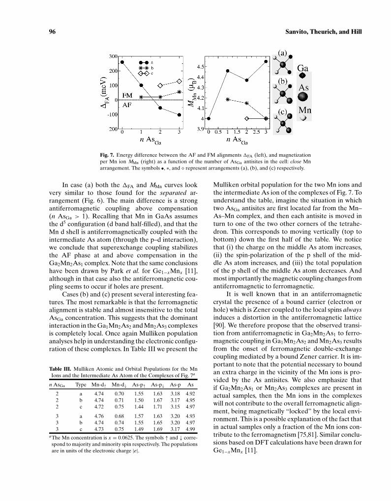
P1: GVG
Journal of Superconductivity: Incorporating Novel Magnetism (JOSC) pp378-josc-367300 January 22, 2002 8:17 Style file version Nov. 07, 2000
96 Sanvito, Theurich, and Hill
Fig. 7. Energy difference between the AF and FM alignments 1FA (left), and magnetizationper Mn ion MMn (right) as a function of the number of AsGa antisites in the cell: close Mnarrangement. The symbols •, ∗, and ¦ represent arrangements (a), (b), and (c) respectively.
In case (a) both the 1FA and MMn curves lookvery similar to those found for the separated ar-rangement (Fig. 6). The main difference is a strongantiferromagnetic coupling above compensation(n AsGa > 1). Recalling that Mn in GaAs assumesthe d5 configuration (d band half-filled), and that theMn d shell is antiferromagnetically coupled with theintermediate As atom (through the p–d interaction),we conclude that superexchange coupling stabilizesthe AF phase at and above compensation in theGa2Mn2As1 complex. Note that the same conclusionshave been drawn by Park et al. for Ge1−xMnx [11],although in that case also the antiferromagnetic cou-pling seems to occur if holes are present.
Cases (b) and (c) present several interesting fea-tures. The most remarkable is that the ferromagneticalignment is stable and almost insensitive to the totalAsGa concentration. This suggests that the dominantinteraction in the Ga1Mn2As2 and Mn2As3 complexesis completely local. Once again Mulliken populationanalyses help in understanding the electronic configu-ration of these complexes. In Table III we present the
Table III. Mulliken Atomic and Orbital Populations for the MnIons and the Intermediate As Atom of the Complexes of Fig. 7a
n AsGa Type Mn-d↑ Mn-d↓ As-p↑ As-p↓ As-p As
2 a 4.74 0.70 1.55 1.63 3.18 4.922 b 4.74 0.71 1.50 1.67 3.17 4.952 c 4.72 0.75 1.44 1.71 3.15 4.97
3 a 4.76 0.68 1.57 1.63 3.20 4.933 b 4.74 0.74 1.55 1.65 3.20 4.973 c 4.73 0.75 1.49 1.69 3.17 4.99
aThe Mn concentration is x = 0.0625. The symbols ↑ and ↓ corre-spond to majority and minority spin respectively. The populationsare in units of the electronic charge |e|.
Mulliken orbital population for the two Mn ions andthe intermediate As ion of the complexes of Fig. 7. Tounderstand the table, imagine the situation in whichtwo AsGa antisites are first located far from the Mn–As–Mn complex, and then each antisite is moved inturn to one of the two other corners of the tetrahe-dron. This corresponds to moving vertically (top tobottom) down the first half of the table. We noticethat (i) the charge on the middle As atom increases,(ii) the spin-polarization of the p shell of the mid-dle As atom increases, and (iii) the total populationof the p shell of the middle As atom decreases. Andmost importantly the magnetic coupling changes fromantiferromagnetic to ferromagnetic.
It is well known that in an antiferromagneticcrystal the presence of a bound carrier (electron orhole) which is Zener coupled to the local spins alwaysinduces a distortion in the antiferromagnetic lattice[90]. We therefore propose that the observed transi-tion from antiferromagnetic in Ga2Mn2As1 to ferro-magnetic coupling in Ga1Mn2As2 and Mn2As3 resultsfrom the onset of ferromagnetic double-exchangecoupling mediated by a bound Zener carrier. It is im-portant to note that the potential necessary to boundan extra charge in the vicinity of the Mn ions is pro-vided by the As antisites. We also emphasize thatif Ga2Mn2As1 or Mn2As3 complexes are present inactual samples, then the Mn ions in the complexeswill not contribute to the overall ferromagnetic align-ment, being magnetically “locked” by the local envi-ronment. This is a possible explanation of the fact thatin actual samples only a fraction of the Mn ions con-tribute to the ferromagnetism [75,81]. Similar conclu-sions based on DFT calculations have been drawn forGe1−xMnx [11].

P1: GVG
Journal of Superconductivity: Incorporating Novel Magnetism (JOSC) pp378-josc-367300 January 22, 2002 8:17 Style file version Nov. 07, 2000
Density Functional Calculations for III–V Semiconductors 97
Fig. 8. (a) AsGa and (b) Asi–VGa pair obtained by moving AsGaalong the 〈111〉 direction.
5.2. Defect Manipulation
In a recent paper [86] we have shown that intrin-sic defect manipulation can provide a valuable way oftuning the carrier concentration and hence enhancingthe Tc in (Ga,Mn)As, without changing the Mn con-centration nor the microscopic configuration of theMn ions. Here we summarize the basic ideas. We firstrecall that isolated AsGa in GaAs are responsible forthe photoquenchable EL2 defect [91]. In fact upon il-lumination, AsGa undergoes a structural transition toan As interstitial–Ga vacancy (Asi–VGa) pair, whichis obtained by moving AsGa along the 〈111〉 direction(see Fig. 8). This complex is metastable since AsGa canbe regenerated by heating. It is crucial to observe thatthe Asi–VGa pair is not electronically active in GaAs,since its only state in the band gap is completely filled.In what follows we show that this metastable complexis present, can be obtained by illumination, and is alsoelectronically inactive in (Ga,Mn)As.
In Fig. 9 we present the total energy and the mag-netization of a 64-atom unit cell containing one Mnion (x = 0.03125) and one AsGa (note that in this casethe system is n doped, with one excess electron perunit cell) as a function of the displacement l〈111〉 ofAsGa along 〈111〉. For comparison we also present the
Fig. 9. Total energy (left-hand-side scale) and magnetization (right-hand-side scale) for (a) (Ga,Mn)As and (b) GaAs as a function ofthe displacement of an AsGa antisite along 〈111〉. The energy ofl〈111〉 = 0 is set to 0 eV.
same curve for GaAs, which is in very good agreementwith previously published results [91]. It is clear thatin (Ga,Mn)As also the Asi–VGa defect is metastableand that the energy barrier for the thermal regen-eration is 0.45 eV. This, according to kinetic calcula-tions [91], gives a regeneration temperature of about100 K.
Having established that the Asi–VGa defect ismetastable let us now prove that it can also begenerated in (Ga,Mn)As. The mechanism has beenexplained by Scheffler et al. [91,92], and can be sum-marized as follows. It is known that the excited a1
1t12
electronic configuration of a tetrahedral substitu-tional double donor induces lattice distortion. Suchdistortion occurs in AsGa, which possesses a doublyoccupied donor level a at midgap and an empty res-onant state with t2 symmetry close to the conduc-tion band edge. The distortion is initiated because themany-electron wave function of the a1
1t12 configura-
tion is orbitally degenerate and therefore the systemis Jahn–Teller unstable. Jahn–Teller distortion splitsthe t2 state into a lower a state (half-filled) and ahigher e state (empty). Therefore an optical excita-tion of the a2
1t02 ground state to the a1
1t12 will initiate
a distortion. It has been demonstrated that in GaAsthe total-energy curve as a function of the displace-ment of AsGa along 〈111〉 for the a1
1t12 configuration
has a minimum for l〈111〉 ∼0.3 A [91]. Then the systemhas some probability of relaxing onto the Asi–VGa
side of the total-energy curve of Fig. 9, ending up con-siderably far from the antisite position, creating theAsi–VGa pair.
The same mechanism holds for (Ga,Mn)As sincethe only difference with respect to GaAs is the spinsplitting of the bands. This splitting, however, does notmove the a state of AsGa into the valence band nor thet2 state into the conduction band. With these consid-erations it is clear that the As antisite in (Ga,Mn)Aspresents the same features as that in GaAs and,therefore, the mechanism described above is stillapplicable.
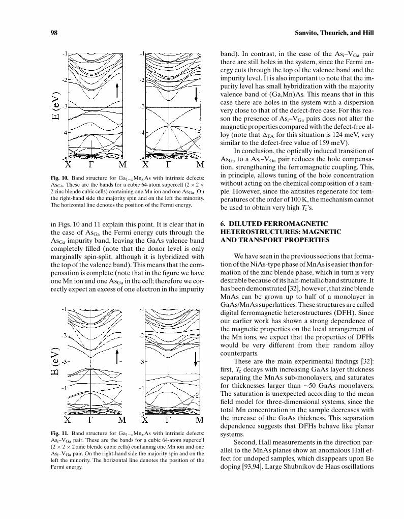
The effects of this transition on the ferromag-netic properties are quite dramatic. We calculate theenergy difference between the ferromagnetic and an-tiferromagnetic alignment,1FA, and we observe an in-crease from 53 to 124 meV when a single AsGa is trans-formed into a Asi–VGa pair. Hence the ferromagneticorder is strengthened. The reason for this enhance-ment of the ferromagnetic coupling is that most of thehole compensation introduced by AsGa is lifted by thecreation of the Asi–VGa pair. The band structures of(Ga,Mn)As containing AsGa and Asi–VGa pair shown
P1: GVG
Journal of Superconductivity: Incorporating Novel Magnetism (JOSC) pp378-josc-367300 January 22, 2002 8:17 Style file version Nov. 07, 2000
98 Sanvito, Theurich, and Hill
Fig. 10. Band structure for Ga1−xMnxAs with intrinsic defects:AsGa. These are the bands for a cubic 64-atom supercell (2× 2×2 zinc blende cubic cells) containing one Mn ion and one AsGa. Onthe right-hand side the majority spin and on the left the minority.The horizontal line denotes the position of the Fermi energy.
in Figs. 10 and 11 explain this point. It is clear that inthe case of AsGa the Fermi energy cuts through theAsGa impurity band, leaving the GaAs valence bandcompletely filled (note that the donor level is onlymarginally spin-split, although it is hybridized withthe top of the valence band). This means that the com-pensation is complete (note that in the figure we haveone Mn ion and one AsGa in the cell; therefore we cor-rectly expect an excess of one electron in the impurity
Fig. 11. Band structure for Ga1−xMnxAs with intrinsic defects:Asi–VGa pair. These are the bands for a cubic 64-atom supercell(2 × 2 × 2 zinc blende cubic cells) containing one Mn ion and oneAsi–VGa pair. On the right-hand side the majority spin and on theleft the minority. The horizontal line denotes the position of theFermi energy.
band). In contrast, in the case of the Asi–VGa pairthere are still holes in the system, since the Fermi en-ergy cuts through the top of the valence band and theimpurity level. It is also important to note that the im-purity level has small hybridization with the majorityvalence band of (Ga,Mn)As. This means that in thiscase there are holes in the system with a dispersionvery close to that of the defect-free case. For this rea-son the presence of Asi–VGa pairs does not alter themagnetic properties compared with the defect-free al-loy (note that 1FA for this situation is 124 meV, verysimilar to the defect-free value of 159 meV).
In conclusion, the optically induced transition ofAsGa to a Asi–VGa pair reduces the hole compensa-tion, strengthening the ferromagnetic coupling. This,in principle, allows tuning of the hole concentrationwithout acting on the chemical composition of a sam-ple. However, since the antisites regenerate for tem-peratures of the order of 100 K, the mechanism cannotbe used to obtain very high Tc’s.
6. DILUTED FERROMAGNETICHETEROSTRUCTURES: MAGNETICAND TRANSPORT PROPERTIES
We have seen in the previous sections that forma-tion of the NiAs-type phase of MnAs is easier than for-mation of the zinc blende phase, which in turn is verydesirable because of its half-metallic band structure. Ithas been demonstrated [32], however, that zinc blendeMnAs can be grown up to half of a monolayer inGaAs/MnAs superlattices. These structures are calleddigital ferromagnetic heterostructures (DFH). Sinceour earlier work has shown a strong dependence ofthe magnetic properties on the local arrangement ofthe Mn ions, we expect that the properties of DFHswould be very different from their random alloycounterparts.
These are the main experimental findings [32]:first, Tc decays with increasing GaAs layer thicknessseparating the MnAs sub-monolayers, and saturatesfor thicknesses larger than ∼50 GaAs monolayers.The saturation is unexpected according to the meanfield model for three-dimensional systems, since thetotal Mn concentration in the sample decreases withthe increase of the GaAs thickness. This separationdependence suggests that DFHs behave like planarsystems.
Second, Hall measurements in the direction par-allel to the MnAs planes show an anomalous Hall ef-fect for undoped samples, which disappears upon Bedoping [93,94]. Large Shubnikov de Haas oscillations

P1: GVG
Journal of Superconductivity: Incorporating Novel Magnetism (JOSC) pp378-josc-367300 January 22, 2002 8:17 Style file version Nov. 07, 2000
Density Functional Calculations for III–V Semiconductors 99
Fig. 12. Band structure for a MnAs1/GaAs15 superlattice: (a) ma-jority and (b) minority spins. X1 and X2 are in the MnAs planeand denote directions along respectively the edge and the diagonalof the cubic supercell. 0→ Z1 is the direction orthogonal to theMnAs plane. The horizontal line indicates the Fermi energy.
are found in doped samples, although surprisingly thecharge densities extracted from the Hall coefficientand from the Shubnikov de Haas oscillations are dif-ferent. This suggests that two different carrier typescould be present in the system.
Density functional theory has answered the fol-lowing questions regarding the physics of DFHs:(i) what is the real dimensionality of the system?(ii) are the carriers spin polarized? (iii) what is thecarrier distribution in the system?
We have used the code SIESTA [95] with a DFH su-perlattice constructed from N GaAs cubic cells (eightatoms in the cell) aligned along the z direction. OneGa plane (two atoms) is substituted with Mn and pe-riodic boundary conditions are applied. This leadsto an infinite MnAs1/GaAs2N−1 superlattice, whereMnAs zinc blende monolayers are separated by a5.65× N A thick GaAs layer. In Fig. 12 we presentthe calculated band structure for the case N = 8 (witha 45.2 A thick GaAs interlayer), for both the major-ity and minority spins. It shows clearly a very pecu-liar half-metallic structure. Although the band struc-ture has a gap for the minority spin and some bandcrossing at the Fermi energy for the majority, theband dispersion in the MnAs plane (X1 → 0→ X2) isquite broad while the one perpendicular to the MnAsplane (Z1 → 0) is very narrow (impurity-like band).Therefore MnAs/GaAs looks like a two-dimensionalhalf-metal with small hopping between the MnAsplanes.
We also look at the stability of the ferromag-netic phase as a function of the separation betweenMn planes, by calculating 1FA. Surprisingly 1FA isindependent of the GaAs thickness for the range ofthicknesses investigated here (531, 533, and 515 meVrespectively for N = 4, N = 6, and N = 8). This isconsistent with the experimental insensitivity of Tc tothe GaAs thickness. This first analysis shows that mostof the physics of DFH occurs in the MnAs planes.
In order to have a better understanding we havealso performed transport calculations in the ballisticlimit. One of the advantages of using a localized basisset for the DFT calculation is that at the end of theself-consistent procedure a tight-binding Hamiltonianis generated by direct numerical integration over areal space grid [53]. Then transport properties canbe calculated in the ballistic limit by using a well-established technique for tight-binding Hamiltonians,which is described in Ref. [96]. For this work, we havegeneralized the technique to the case of nonorthogo-nal tight-binding models with singular coupling ma-trices [95]. More details can be found in the citedliterature.
In Fig. 13 we present our calculated conductanceper unit area as a function of the position of the Fermienergy for an MnAs1/GaAs15 superlattice for boththe current in the MnAs plane (CIP) and the cur-rent perpendicular to the Mn plane (CPP) directions,and for both spins. We also project the conductanceonto the atomic orbital basis set in order to deter-mine the orbital character of the electrons carrying
Fig. 13. Total and partial conductance per unit area for aMnAs1/GaAs15 superlattice as a function of the position of theFermi energy for majority (↑) and minority (↓) spin bands. Thevertical line denotes the position of the Fermi energy for undopedsamples.

P1: GVG
Journal of Superconductivity: Incorporating Novel Magnetism (JOSC) pp378-josc-367300 January 22, 2002 8:17 Style file version Nov. 07, 2000
100 Sanvito, Theurich, and Hill
the current [96]. As expected from the band struc-ture, the ballistic current is 100% spin polarized, withno current for the minority spin band. In the major-ity spin band the behavior is very different for theCIP and CPP alignment. In the CIP case the con-ductance is quite large and independent of the en-ergy, with a significant contribution (roughly 20% ofthe total conductance) coming from the Mn d t2 or-bitals. In contrast, the conductance is very small inthe CPP direction, with orbital contribution almostentirely from the As p states. Moreover the conduc-tance at EF comes from just a few k-points around the0 point (in the direction orthogonal to the transport).These correspond to the states with the largest kineticenergy in the direction of the transport. This situationis similar to that occurring in tunneling junctions andso we describe the transport as tunneling-like, mean-ing that the transport in the CPP direction is throughhopping between the MnAs planes.
Finally we investigate the spatial distribution ofthe current. This is given by the charge density dis-tribution in real space, ρ(r), calculated only for thosestates contributing to the conductance (see Fig. 14)[95]. The figure confirms that the current in the CIPcase is distributed mainly in a narrow region aroundthe MnAs planes, with small spillage outside. In con-trast, the CPP current is mainly located at the Mnplane with small contributions from the GaAs layers.This means that carriers are strongly confined in the
Fig. 14. Charge density distribution in real space for MnAs1/GaAs15 (a) calculated only for those states contributing to the con-ductance and energy within 0.3 eV from EF: CIP (b) and CPP (c)configurations.
MnAs plane and the perpendicular transport is viahopping between the planes.
DFT has therefore answered all the questionsstated at the beginning of this section. The DFHsappear to be two-dimensional half-metals, with ametallic-like ballistic conductance in the MnAsplane and an hopping conductance perpendicular tothe MnAs planes. The ferromagnetism is thereforeinsensitive to the GaAs layer thickness, showing nodilution effect.
7. OTHER DILUTED MAGNETICSEMICONDUCTORS
So far we have concentrated primarily on theproperties of (Ga,Mn)As, which is the most well stud-ied of the DMSs. However, in the last year severalother DMSs have been synthesized, some of themshowing remarkably high Tc. At the same time sev-eral DFT calculations have been published both ex-plaining the properties of existing materials or makingpredictions for new ones. The prediction of materialproperties in advance of experiments is one of themost important aspects of density functional theory.Here we review the principal works in this area.
7.1. Ga1−xMxAs with M = V, Cr, Fe
Doping of GaAs with transition metals otherthan Mn has been investigated theoretically usingboth the full-potential linearized augmented planewave (FLAPW) method [61] and the atomic sphereapproximation [70]. Since the first method is compu-tationally more demanding the author concentrateson the electronic structure of hypothetical zinc blendeMAs with M=V, Cr, Mn, Fe, and on the high concen-tration limit of Ga1−xMxAs (x = 0.25 and x = 0.125).The main result is that while the ground state of FeAsis antiferromagnetic, VAs, CrAs, and MnAs at the re-spective equilibrium lattice constants appear to behalf-metallic ferromagnets with magnetic momentsrespectively of 2µB, 3µB, and 4µB per formula unit.
Turning attention to Ga1−xMxAs it is interest-ing to note that the calculated DOS for Ga1−xVxAsin the large concentration limit reveals very smallhybridization of the V 3d orbitals with the GaAsvalence band, suggesting that in this compound themagnetic coupling may be rather small. In con-trast, Ga1−xCrxAs shows a DOS very similar tothat of Ga1−xMnxAs. This suggests that Ga1−xCrxAs

P1: GVG
Journal of Superconductivity: Incorporating Novel Magnetism (JOSC) pp378-josc-367300 January 22, 2002 8:17 Style file version Nov. 07, 2000
Density Functional Calculations for III–V Semiconductors 101
may be a potential candidate for a high Tc DMS.In addition van Schilfgaarde and Mryasov fit theirDFT results with a pairwise Heisenberg-like en-ergy E = −∑i j Ji j Esi · Es j , and found that the val-ues of J for Ga1−xCrxAs are larger than those ofGa1−xMnxAs. This suggests stronger ferromagnetismfor Ga1−xCrxAs than for Ga1−xMnxAs. However thisprediction is strongly affected by the fact that theDFT results strongly deviate from the Heisenberg-like form.
Experimentally both Ga1−xFexAs [97] andGa1−xCrxAs [98] have been synthesized and there isa little evidence for ferromagnetic order. Howeververy recently zinc blende CrAs has been successfullygrown on GaAs at low temperature [99], showing a Tc
above room temperature. Moreover preliminary mea-surements show a magnetic moment per formula unitvery close to 3µB, in good agreement with the theo-retical predictions [61]. To our knowledge Ga1−xVxAshas never been grown.
7.2. Ga1−xMnxN
There has been a large effort in synthesizingGa1−xMnxN in the last two years, since Dietl et al. pre-dicted a Curie temperature higher than any other Mn-doped semiconductors for this compound [17]. Veryrecently this prediction has been confirmed experi-mentally [10], with Ga1−xMnxN at 10% Mn concen-tration showing a remarkably large Tc (940 K). Un-fortunately the mechanism for the ferromagnetism inGa1−xMnxN is not clearly understood because of thelack of experimental data. In particular the natureand the role of the free carriers (if present) are notyet clear.
Sato and Katayama-Yoshida performed DFTcalculations within the KKR-CPA method [100]. Theylooked at transition-metal doping of GaN and stud-ied the stability of the ferromagnetic configurationagainst the spin glass state. The ferromagnetic stateappears to be stable for (Ga,V)N and (Ga,Cr)N, whilefor (Ga,Fe)N, (Ga,Co)N, and (Ga,Ni)N the spin glassstate has lower total energy at every concentrationsstudied (x = 0.05, 0.1, 0.15, 0.20, 0.25). The case of(Ga,Mn)N is critical since the ferromagnetic state isstable only at low Mn concentration (x < 0.15). Thisis explained in terms of competition between doubleexchange and superexchange, with the latter beingdominant for small Mn–Mn separations.
The DOS of (Ga,Mn)N looks rather differentthan that of (Ga,Mn)As, showing a much stronger
d contribution at the Fermi energy and smaller p–dhybridization. This leads to the formation of an Mn dimpurity band in the band gap of GaN, as calculatedby Kronik et al. [101], who also calculated that the(Ga,Mn)N valence band is not spin split. The atomicconfiguration of Mn is calculated to be Mn3+ with thed orbitals arranging as d4 [100]. This contradicts theexperimental results for paramagnetic (Ga,Mn)As[102], which convincingly show a d5 (S = 5/2) config-uration. The reasons of this discrepancy are not clearat the moment.
7.3. Zn1−xMxO with M = V, Cr, Mn, Fe, Co, Ni
The mean field model of Dietl et al. also predictsa very large Tc for Mn-doped ZnO [17], provided thatthe sample is p doped. Sato and Katayama-Yoshidaalso investigated the stability of the ferromagneticphase with respect to the spin glass phase forZn1−xMxO (M = V, Cr, Mn, Fe, Co, Ni), again usinga KKR-CPA method [103–105]. They found a ferro-magnetic ground state for all the materials except Mn,for which the spin glass configuration has a lower en-ergy. However they also showed that in the case ofMn the ferromagnetic configuration can be obtainedby large p doping (they substitute N atoms at the Osites in their calculations).
Since in the II–VI semiconductors only verysmall hole concentrations can be obtained by doping,they also investigated the conditions to have strongferromagnetism in transition-metal-doped ZnO withadditional n doping (Ga at the Zn sites). The resultof this calculation is that the presence of electronsstabilizes the ferromagnetic order in ZnO dopedwith Fe, Co, and Ni [104]. It is important to notethat in all these cases the Mn d shell is more thanhalf-filled and that the Fermi energy is located withinan Mn d region of the minority spin density of states.These are the conditions for strong double-exchangecoupling between the transition-metal ions. The factthat n-doped (Zn,Co)O [14] and (Zn,Ni)O [106] havebeen grown, showing Tc’s above room temperature,is very encouraging.
Similar calculations have been carried outfor transition-metal-doped ZnS, ZnSe, and ZnTe[107,108] without any additional doping. These showthat only V- and Cr-doped materials have a fer-romagnetic ground state, which is due to double-exchange coupling. In this case the carriers mediat-ing the double exchange are holes at the top of thevalence band, which in turn are strongly hybridized

P1: GVG
Journal of Superconductivity: Incorporating Novel Magnetism (JOSC) pp378-josc-367300 January 22, 2002 8:17 Style file version Nov. 07, 2000
102 Sanvito, Theurich, and Hill
with the p states of the group VI element. It is worthmentioning that to date no ferromagnetic order hasbeen found experimentally in these materials. How-ever real samples present strong self-compensation,which suppresses the hole-mediated double-exchangemechanism.
7.4. M1−xMnxGeII2 with M = Cd, Znand II = P, As
Cd1−xMnxGeP2 was the first room temperaturediluted ferromagnetic semiconductors to be grown[12]. It has a body-centered tetragonal cell, and themain advantage of this structure is that Mn can sub-stitute for the II cations, adopting the Mn2+ state(“natural” for Mn). Accurate calculations with bothGGA and LDA have been performed [109,110],showing that indeed Mn assumes an Mn2+ state. Thecalculations demonstrate a very weak sensitivity ofthe magnetic and electronic structure on both the an-ion (As or P) and cation (Cd or Zn) elements.
Interestingly both the LDA and GGA resultsgive an antiferromagnetic ground state, contradictingthe experimental results. However two aspects mustbe pointed out. First, the samples in the experiments[12] are prepared with vacuum deposition on a sin-gle crystal surface, followed by solid-state reaction athigh temperature. This means that most of the Mn ionsare located close to the surface. The DFT calculationsare performed for perfect crystalline bulk systems,whose properties will certainly differ from those ofthe actual samples. Second, it has been demonstrated[110] that the ferromagnetic phase can become sta-ble against the antiferromagnetic one, if electrons areintroduced in the system (S substituting for P). Thisseems to suggest that the presence of free carriers isalso essential for ferromagnetic order in chalcopyritesemiconductors.
Finally, very recently Mahadevan and Zungercalculated the formation energies of several intrin-sic defects of CdGeP2, of Mn impurities in CdGeP2
either at the Cd or at the Ge site, and of complexesof these [111]. They found that under Cd-, Mn-, andP-rich growth conditions, MnGe impurities naturallyform in the crystal. These impurities, that in contrastto Mn in GaAs do not form clusters, are acceptorsin CdGeP2 and align ferromagnetically. In addition itis important to observe that the ferromagnetic cou-pling is also found between MnGe and MnCd impuri-ties. These predictions offer very good guidelines forgrowing room-temperature Mn-doped CdGeP2.
8. CONCLUSIONS ANDFUTURE DIRECTIONS
In this paper we have presented the re-cent DFT contributions to the physics of dilutedmagnetic semiconductors. Most of the results are for(Ga,Mn)As, have been obtained within either theLSDA or the GGA approximation, and capture mostof the relevant physics of (Ga,Mn)As. We have alsosummarize the latest results for other DMSs, whoseproperties are less well studied and understood.
During these studies several disagreements withexperiments have appeared, suggesting that in somecases the LSDA/GGA approximations may be notcompletely appropriate. It is therefore indispens-able to understand the limit of the reliability ofthe LSDA/GGA approximations and eventually tocorrect them. It is well known that the local den-sity approximation fails in describing systems whereelectron–electron interaction is strong. This gener-ally happens when we try to describe orbitals tightlybound to their nuclei. The d orbitals of transition met-als in transition-metal oxides are an example of this.
A typical signature of the inappropriateness ofthe LSDA/GGA is that the bands from tightly boundorbitals are pushed toward higher energies. This cancreate the following problems in DMSs: (1) underes-timation of the true band occupation, leading to anerroneous magnetic moment, (2) overestimation ofp–d interaction, due to artificially strong hybridiza-tion, (3) overbinding of the structure, (4) tendency tometallicity in otherwise semiconducting systems, and(5) prediction of the wrong magnetic state (i.e. fer-romagnetic instead of antiferromagnetic). All theseproblems can of course strongly affect the predictionsof DFT calculations, and they must be corrected.
Several schemes have been adopted to go beyondthe LSDA/GGA approximation, and here we brieflylist them. In 1981 Perdew and Zunger [44] showedthat most of the problems of the LDA approximationcome from its incorrect treatment of coulombic self-interaction. They demonstrated that self-interactioncorrections, namely the subtraction of spurious self-interaction from the density functional, greatly im-prove the description of localized states. Since thenseveral implementations have been made [112] in-cluding algorithms using pseudopotentials [113].
A quite different approach to this problem isrepresented by the LDA+U scheme [42,43]. Themain idea is to combine density functional theorywith an Hubbard description of those orbitals whichsuffer strong correlations. In this case an additional
P1: GVG
Journal of Superconductivity: Incorporating Novel Magnetism (JOSC) pp378-josc-367300 January 22, 2002 8:17 Style file version Nov. 07, 2000
Density Functional Calculations for III–V Semiconductors 103
Hubbard-like term is added to the energy functionaland the consequent single-particle equations are de-duced. The theory gain two extra parameters (theHubbard parameter U and the Hund’s rule exchangeJ ), which can be fixed from experimental values orcalculated self-consistently. The advantages of theLDA+U scheme are the relatively easy numerical im-plementation and the fact that the parameters can bedirectly compared with those coming from simplermodels.
In conclusion, we have shown that DFT can bea very powerful tool for describing structural, elec-tronic, magnetic, and transport properties of dilutedmagnetic semiconductors. In particular DFT is veryuseful for obtaining parameters not accessible fromexperiments, and for providing accurate descriptionsof properties occurring at the atomic scale. The predic-tion of new materials with novel properties is possible,although special care should be taken in order to keeperrors coming from the local density approximationunder control.
ACKNOWLEDGMENTS
We thank S. Picozzi, L. Kronik, S. Hellberg,P. Mahadevan, and B. I. Min for useful discussions,comments, and permission to discuss unpublished re-sults. This work made use of MRL Central Facilitiessupported by the National Science Foundation underaward No. DMR96-32716. This work is supported byONR Grant N00014-00-10557, by NSF-DMR underthe Grant 9973076, and by ACS PRF under the Grant33851-G5.
REFERENCES
1. G. Prinz, Science 282, 1660 (1998); G. Prinz, Phys. Today 48,58 (1995).
2. M. N. Baibich, J. M. Broto, A. Fert, F. Nguyen Van Dau,F. Petroff, P. Etienne, G. Creuzet, A. Friederich, andJ. Chazelas, Phys. Rev. Lett. 61, 2472 (1988); G. Binasch,P. Grunberg, F. Sauerbach, and W. Zinn, Phys. Rev. B 39, 4828(1989).
3. H. X. Tang, F. G. Monzon, R. Lifshitz, M. C. Cross, andM. L. Roukes, Phys. Rev. B 61, 4437 (2000), and referencestherein.
4. W. Y. Lee, S. Gardelis, B. C. Choi, Y. B. Xu, C. G. Schmidt,C. H. W. Barnes, D. A. Ritchie, E. H. Linfield, and J. A. C.Bland, Appl. Phys. Lett. 85, 6682 (1999).
5. P. R. Hammar, B. R. Bennet, M. J. Yang, and M. Johnson,Phys. Rev. Lett. 83, 203 (1999).
6. G. Schmidt, D. Ferrand, L. W. Molenkamp, A. T. Filip, andB. J. van Wees, Phys. Rev. B 62, R4790 (2000).
7. P. R. Hammar and M. Johnson, Appl. Phys. Lett. 79, 2591(2001).
8. H. Ohno, J. Magn. Magn. Mater 200, 110 (1999); H. Ohno,Science 281, 951 (1998).
9. H. Ohno, H. Munekata, T. Penney, S. von Molnar, andL. L. Chang, Phys. Rev. Lett. 68, 2664 (1992).
10. S. Sonoda, S. Shimizu, T. Sasaki, Y. Yamamoto, and H. Hori,cond-mat/0108159.
11. Y. D. Park, A. T. Hanbicki, S. C. Erwin, C. S. Hellberg, J. M.Sullivan, J. E. Mattson, T. F. Ambrose, A. Wilson, G. Spanos,and B. T. Jonker, preprint.
12. G. A. Medvedkin, T. Ishibashi, T. Nishi, K. Hayata,Y. Hasegawa, and K. Sato, Jpn. J. Appl. Phys. 39, L949(2000).
13. Y. Matsumoto, M. Murakami, T. Shono, T. Hasegawa,T. Fukumura, M. Kawasaki, P. Ahmet, T. Chikyow, S.-Ya.Koshihara, and H. Koinuma, Science 291, 854 (2001).
14. K. Ueda, H. Tabata, and T. Kawai, Appl. Phys. Lett. 79, 988(2001).
15. Y. Ohno, D. K. Young, B. Beschoten, F. Matsukura, H. Ohno,and D. D. Awschalom, Nature 402, 790 (1999).
16. H. Ohno, D. Chiba, F. Matsukura, T. Omiya, E. Abe, T. Dietl,Y. Ohno, and K. Ohtani, Nature 408, 944 (2000).
17. T. Dietl, H. Ohno, F. Matsukura, J. Cibert, and D. Ferrand,Science 287, 1019 (2000); T. Dietl, H. Ohno, and F. Matsukura,Phys. Rev. B 63, 195205 (2001).
18. T. Jungwirth, W. A. Atkinson, B. H. Lee, and A. H.MacDonald, Phys. Rev. B 59, 9818 (1999).
19. J. Szczytko, W. Mac, A. Stachow, A. Twardowski, P. Becla, andJ. Tworzydlo, Solid State Commun. 99, 927 (1996).
20. K. Ando, T. Hayashi, M. Tanaka, and A. Twardowski, J. Appl.Phys. 83, 6548 (1998).
21. J. Szczytko, W. Mac, A. Twardowski, F. Matsukura, andH. Ohno, Phys. Rev. B 59, 12935 (1999).
22. F. Matsukura, H. Ohno, A. Shen, and Y. Sugawara, Phys. Rev.B 57, R2037 (1998).
23. T. Omiya, F. Matsukura, T. Dietl, Y. Ohno, T. Sakon,M. Motokawa, and H. Ohno, Physica E 7, 976 (2000).
24. J. Okabayashi, A. Kimura, O. Rader, T. Mizokawa,A. Fujimori, T. Hayashi, and M. Tanaka, Phys. Rev. B 58,R4211 (1998).
25. T. Hayashi, Y. Hashimoto, S. Katsumoto, and Y. Iye, Appl.Phys. Lett. 78, 1691 (2001).
26. S. J. Potashnik, K. C. Ku, S. H. Chun, J. J. Berry, N. Samarth,and P. Schiffer, Appl. Phys. Lett. 79, 1495 (2001).
27. H. Hohenberg and W. Kohn, Phys. Rev. 136, B864 (1964).28. W. Kohn and L. J. Sham, Phys. Rev. 140, A1133 (1965).29. G. B. Bachelet, D. R. Hamann, and M. Schluter, Phys. Rev. B
26, 4199 (1982).30. O. F. Sankey and D. J. Niklewski, Phys. Rev. B 40, 3979 (1989).31. P. Ordejon, Phys. Stat. Sol. B 217, 335 (2000).32. R. K. Kawakami, E. Johnston-Halperin, L. F. Chen,
M. Hanson, N. Guebels, J. S. Speck, A. C. Gossard, andD. D. Awschalom, Appl. Phys. Lett. 77, 2379 (2000).
33. M. T. Yin and M. L. Cohen, Phys. Rev. B 26, 5668 (1982).34. J. Neugebauer and M. Scheffler, Phys. Rev. B 46, 16067 (1992).35. J. F. Janak and A. R. Williams, Phys. Rev. B 14, 4199 (1976).36. C. S. Wang and J. Callaway, Phys. Rev. B 15, 298 (1977).37. V. L. Moruzzi, A. R. Williams, and J. F. Janak, Phys. Rev. B 15,
2854 (1997).38. K. Schwarz and P. Mohn, J. Phys. F 14, L129 (1984).39. V. L. Moruzzi, P. M. Marcus, K. Schwarz, and P. Mohn, Phys.
Rev. B 34, 1784 (1986).40. C.-L. Fu and K.-M. Ho, Phys. Rev. B 28, 5480 (1983).41. D. Singh, Planewaves, Pseudopotentials and the LAPW
Method (Kluwer Academic, DO 1994), 115 pp.42. V. I. Anisimov, J. Zaanen, and O. K. Andersen, Phys. Rev. B
44, 943 (1991).43. V. I. Anisimov, F. Aryasetiawan, and A. I. Liechtenstein,
J. Phys.: Condens. Matter 9, 767 (1997).44. J. P. Perdew and A. Zunger, Phys. Rev. B 23, 5048 (1981).
P1: GVG
Journal of Superconductivity: Incorporating Novel Magnetism (JOSC) pp378-josc-367300 January 22, 2002 8:17 Style file version Nov. 07, 2000
104 Sanvito, Theurich, and Hill
45. DoD: Department of Defense-planewave; URL: http://cst-www.nrl.navy.mil/people/singh/planewave.
46. The ABINIT code is a common project of the UniversiteCatholique de Louvain, Corning Incorporated, and other con-tributors; URL: http://www.mapr.ucl.ac.be/ABINIT.
47. G. Theurich, B. Anson, N. A. Hill, and A. Hill, Computingin Science and Engineering, p. 22, Jan/Feb 2001. SPINOR ispublically available at http://spinor.sourceforge.net.
48. http://www.gnu.org/copyleft/gpl.txt.49. VASP: Vienna Ab initio Simulation Package; URL: http://
cms.mpi.univie.ac.at/vasp/.50. http://www.accelrys.com.51. M. C. Payne, X. Weng, B. Hammer, G. Francis, U. Bertram,
A. de Vita, J. S. Lin, V. Milman, and A. Qteish, unpublishedmanuscript.
52. P. Ordejon, D. Sanchez-Portal, E. Artacho, and J. M. Soler,SIESTA: Spanish Initiative for Electronic Simulations withThousands of Atoms; URL: http://www.uam.es/siesta/.
53. D. Sanchez-Portal, P. Ordejon, E. Artacho, and J. M. Soler,Internat. J. Quantum Chem. 65, 453 (1997), and referencestherein.
54. O. K. Anderson, Phys. Rev. B 12, 3060 (1975).55. J. Korringa, Physica 13, 392 (1947); W. Kohn and N. Rostocker,
Phys. Rev. 94, 1111 (1954).56. P. Blaha, K. Schwarz, and J. Luitz, WIEN97: A Full Poten-
tial Linearized Augmented Plane Wave Package for Calcu-lating Crystal Properties (Karlheinz Schwarz, Techn. Univ.Wien, Vienna, 1999). ISBN 3-9501031-0-4. See also URL:http://www.tuwien.ac.at/theochem/wien97.
57. http://www.mpi-stuttgart.mpg.de/andersen/.58. M. Shirai, T. Ogawa, I. Kitagawa, and N. Suzuki, J. Magn.
Magn. Mater. 177–181, 1383 (1998).59. T. Ogawa, M. Shirai, N. Suzuki, and I. Kitagawa, J. Magn.
Magn. Mater. 196/197, 428 (1999).60. S. Sanvito and N. A. Hill, Phys. Rev. B 62, 15553 (2000).61. M. Shirai, Physica E 10, 143 (2001).62. A. Continenza, S. Picozzi, W. T. Geng, and A. J. Freeman,
Phys. Rev. B 64, 085204 (2001).63. M. Jain, L. Kronik, J. R. Chelikowsky, and V. V. Godlevsky,
Phys. Rev. B 64, 245205 (2001).64. J. H. Park, S. K. Kwon, and B. I. Min, J. Magn. Magn. Mater.
281/282, 703 (2000).65. B. I. Min, private communication (2001).66. J. R. Schrieffer and P. A. Wolff, Phys. Rev. 149, 491 (1966).67. G. Theurich and N. A. Hill, Phys. Rev. B 64, 073106 (2001).68. S. Sanvito, P. Ordejon, and N. A. Hill, Phys. Rev. B 63, 165206
(2001).69. T. C. Schulthess and W. H. Butler, J. Appl. Phys. 89, 7021
(2001).70. M. van Schilfgaarde and O. N. Mryasov, Phys. Rev. B 63,
233205 (2001).71. Y.-J. Zhao, W. T. Geng, K. T. Park, and A. J. Freeman, Phys.
Rev. B 64, 035207 (2001).72. H. Akai, Phys. Rev. Lett. 81, 3002 (1998).73. R. S. Mulliken, J. Chem. Phys. 23, 1833 (1955).74. R. S. Mulliken, J. Chem. Phys. 23, 1841 (1955).75. H. Ohldag, V. Solinus, F. U. Hillebrecht, J. B. Goedkoop,
M. Finazzi, F. Matsukura, and H. Ohno, Appl. Phys. Lett. 76,2928 (2000).
76. J. K. Furdyna and J. Kossut, eds., Semiconductor andSemimetals, Vol. 25: Diluted Magnetic Semiconductors (Aca-demic, New York, 1988); M. Balkanski and M. Averous,eds., Diluted Magnetic Semiconductors (Plenum, New York,1991).
77. V. G. Abrammishvili, S. I. Gubarev, A. V. Komarov, andS. M. Ryabchenko, Fiz. Tverd. Tela 26, 1095 (1984) [Sov. Phys.Solid State 26, 666 (1984)].
78. S. I. Gubarev and M. G. Tyazhlov, Fiz. Tverd. Tela 32, 635(1990) [Sov. Phys. Solid State 32, 373 (1990)].
79. S. I. Gubarev and M. G. Tyazhlov, Pis’ma Zh. Eksp. Teor. Fiz.44, 385 (1986) [JEPT Lett. 44, 494 (1986)].
80. C. Benoit a la Guillaume, D. Scalbert, and T. Dietl, Phys. Rev.B 46, 9853 (1992).
81. A. Oiwa, S. Kutumoto, A. Endo, M. Hirasawa, Y. Iye, H. Ohno,F. Matsukura, A. Shen, and Y. Sugawara, Solid State Commun.103, 209 (1997).
82. S. B. Zhang, S.-H. Wei, and A. Zunger, Phys. Rev. B 52, 13975(1995).
83. A. Chattopadhyay, S. Das Sarma, and A. J. Millis, cond-mat/0106455.
84. P. Specht, R. C. Lutz, R. Zhao, E. R. Weber, W. K. Liu,K. Bacher, F. J. Towner, T. R. Stewart, and M. Luysberg,J. Vac. Sci. Technol. B 17, 1200 (1999).
85. S. Sanvito and N. A. Hill, Appl. Phys. Lett. 78, 3493 (2001).86. S. Sanvito and N. A. Hill, J. Mag. Mag. Mater. (submitted-a).87. S. Sanvito and N. A. Hill, J. Mag. Mag. Mater. (submitted-b).88. P. W. Anderson, Phys. Rev. 79, 350 (1950).89. H. Akai and P. H. Dederichs, Phys. Rev. B 47, 8739 (1993).90. P.-G. de Gennes, Phys. Rev. 118, 141 (1960).91. J. Dabrowski and M. Scheffler, Phys. Rev. B 40, 10391 (1989).92. M. Scheffler, F. Beeler, O. Jepsen, O. Gunnarsson, O. K.
Anderesen and G. B. Bachelet, in Proceedings of the 13th In-ternational Conference on Defects in Semiconductors, L. C.Kimerling and J. M. Parsey Jr., eds. (The Metallurgical Soci-ety of AIME, New York, 1984), p. 45.
93. G. Zanelatto, T. Kreutz, R. K. Kawakami, E. Johnston-Halperin, E. Gwinn, D. D. Awschalom, and A. C. Gossard,Bull. Am. Phys. Soc. 46, 509 (2001).
94. T. Kreutz, G. Zanelatto, R. K. Kawakami, E. Johnston-Halperin, E. Gwinn, D. D. Awschalom, and A. C. Gossard,Bull. Am. Phys. Soc. 46, 510 (2001).
95. S. Sanvito and N. A. Hill, cond-mat/0108406.96. S. Sanvito, C. J. Lambert, J. H. Jefferson, and A. M. Bratkovsky,
Phys. Rev. B 59, 11936 (1999).97. R. Moriya, Y. Katsumata, Y. Takatani, S. Haneda, T. Kondo,
and H. Munekata, Physica E 10, 224 (2001).98. H. Saito, W. Zaets, R. Akimoto, K. Ando, Y. Mishima, and
M. Tanaka, J. Appl. Phys. 89, 7392 (2001).99. H. Akinaga, T. Manago, and M. Shirai, Jpn. J. Appl. Phys. 39,
L1118 (2000).100. K. Sato and H. Katayama-Yoshida, Jpn. J. Appl. Phys. 40,
L485 (2001).101. L. Kronik, M. Jain, and J. R. Chelikowsky, preprint.102. M. Zajac, J. Gosk, M. Kaminska, A. Twardowski, T. Szyszko,
and S. Podsiadlo, Appl. Phys. Lett. 79, 2432 (2001).103. K. Sato and H. Katayama-Yoshida, Jpn. J. Appl. Phys. 39,
L555 (2000).104. K. Sato and H. Katayama-Yoshida, Jpn. J. Appl. Phys. 40,
L334 (2001).105. K. Sato and H. Katayama-Yoshida, Physica E 10, 251 (2001).106. T. Wakano, N. Fujimura, Y. Morinaga, N. Abe, A. Ashida, and
T. Ito, Physica E 10, 260 (2001).107. K. Sato and H. Katayama-Yoshida, Jpn. J. Appl. Phys. 40,
L651 (2001).108. H. Shoren, F. Ikemoto, K. Yoshida, N. Tanaka, and
K. Motizuki, Physica E 10, 242 (2001).109. Y. J. Zhao, W. T. Geng, A. J. Freeman, and T. Oguchi, Phys.
Rev. B 63, 201202 (2001).110. Y. J. Zhao, S. Picozzi, A. Continenza, W. T. Geng, and A. J.
Freeman, preprint.111. P. Mahadevan and A. Zunger, cond-mat/0111570.112. A. Svane and O. Gunnarsson, Phys. Rev. Lett. 65, 1148 (1990).113. D. Vogel, P. Kruger, and J. Pollmann, Phys. Rev. B 54, 5495
(1996).


![Cyclosporine oral solution [MODIFIED] diluted with orange](https://img.pdfslide.us/doc/110x75/61c6faa1af22391b7f5175cd/cyclosporine-oral-solution-modified-diluted-with-orange-.jpg)


