Embed Size (px)
Citation preview
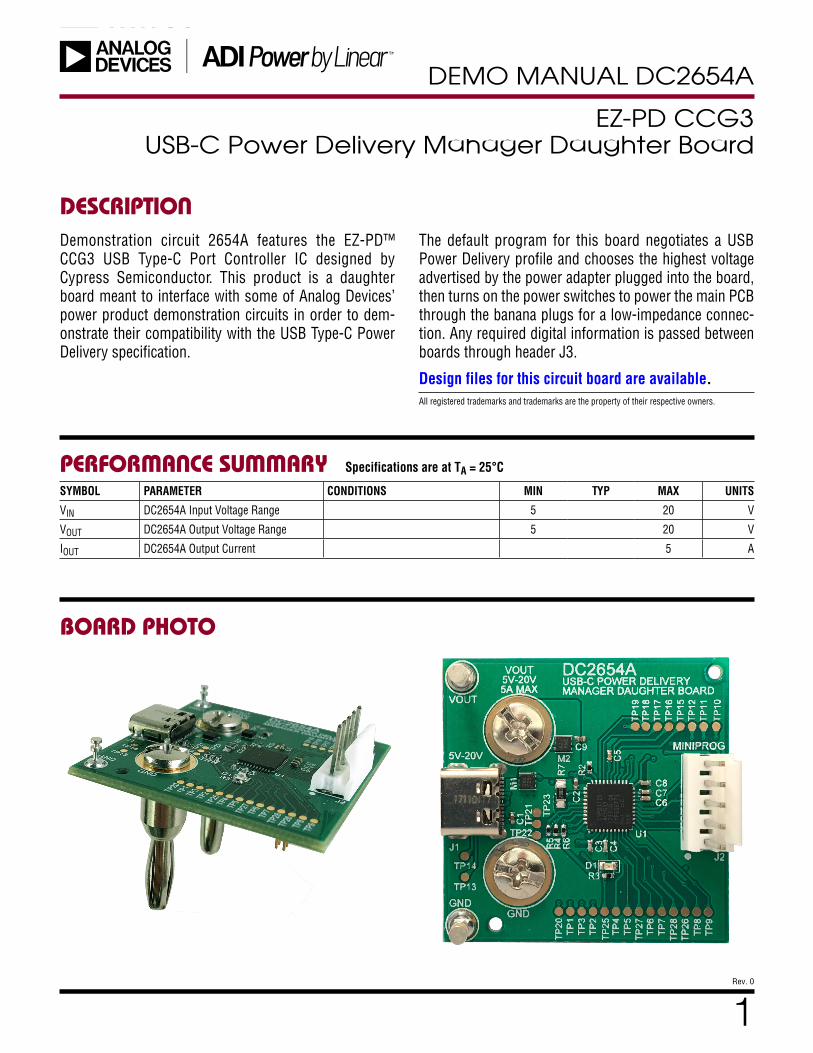
SYMBOL PARAMETER CONDITIONS MIN TYP MAX UNITS
VIN DC2654A Input Voltage Range 5 20 V
VOUT DC2654A Output Voltage Range 5 20 V
IOUT DC2654A Output Current 5 A
1
DEMO MANUAL DC2654A
Rev. 0
DESCRIPTION
EZ-PD CCG3 USB-C Power Delivery Manager Daughter Board
Demonstration circuit 2654A features the EZ-PD™ CCG3 USB Type-C Port Controller IC designed by Cypress Semiconductor. This product is a daughter board meant to interface with some of Analog Devices’ power product demonstration circuits in order to dem-onstrate their compatibility with the USB Type-C Power Delivery specification.
All registered trademarks and trademarks are the property of their respective owners.
PERFORMANCE SUMMARY
BOARD PHOTO
The default program for this board negotiates a USB Power Delivery profile and chooses the highest voltage advertised by the power adapter plugged into the board, then turns on the power switches to power the main PCB through the banana plugs for a low-impedance connec-tion. Any required digital information is passed between boards through header J3.
Design files for this circuit board are available.
Specifications are at TA = 25°C
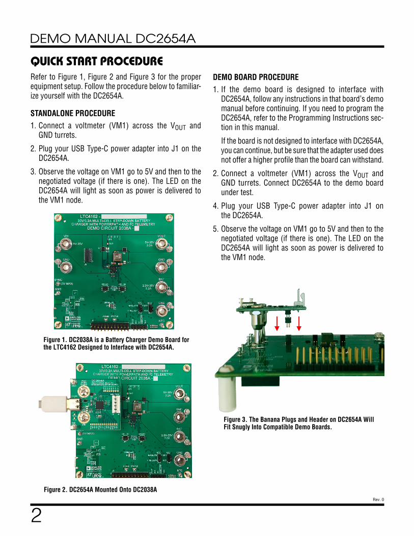
Refer to Figure 1, Figure 2 and Figure 3 for the proper equipment setup. Follow the procedure below to familiar-ize yourself with the DC2654A.
STANDALONE PROCEDURE1. Connect a voltmeter (VM1) across the VOUT and
GND turrets.
2. Plug your USB Type-C power adapter into J1 on the DC2654A.
3. Observe the voltage on VM1 go to 5V and then to the negotiated voltage (if there is one). The LED on the DC2654A will light as soon as power is delivered to the VM1 node.
DEMO BOARD PROCEDURE1. If the demo board is designed to interface with
DC2654A, follow any instructions in that board’s demo manual before continuing. If you need to program the DC2654A, refer to the Programming Instructions sec-tion in this manual.
If the board is not designed to interface with DC2654A, you can continue, but be sure that the adapter used does not offer a higher profile than the board can withstand.
2. Connect a voltmeter (VM1) across the VOUT and GND turrets. Connect DC2654A to the demo board under test.
4. Plug your USB Type-C power adapter into J1 on the DC2654A.
5. Observe the voltage on VM1 go to 5V and then to the negotiated voltage (if there is one). The LED on the DC2654A will light as soon as power is delivered to the VM1 node.
Figure 1. DC2038A is a Battery Charger Demo Board for the LTC4162 Designed to Interface with DC2654A.
Figure 2. DC2654A Mounted Onto DC2038A
Figure 3. The Banana Plugs and Header on DC2654A Will Fit Snugly Into Compatible Demo Boards.
2
DEMO MANUAL DC2654A
Rev. 0
QUICK START PROCEDURE

DEFAULT PROGRAMThe factory-default program on DC2654A is based on the CYPD3125-40LQXI_notebook example project that comes with the EZ-PD CCG3 SDK. The main differences are the addition of variable sink power profile and the operation of the on-board LED. The LED (D1) operates as shown in Table 1.Table 1. LED (D1) OperationLED STATE BOARD STATUS
Off Power Switches Off, Load Has No Power
On Power Switches On, Load Has at Least 5V
Blinking SMBAlert Is Asserted Low
SOURCE MOSFETsComponents M5, M6, R8, and R9 are left unpopulated by default, making DC2654A operate as a sink-only device. In order to operate as a source, these compo-nents can be purchased separately and installed to the
relevant footprints. Table 2 shows the part numbers for these components.Table 2. Part Number for Source Components
COMPONENT MANUFACTURER PART NUMBERM5, M6 Toshiba SSM6K513NU, LFR8, R9 Any 10MΩ 0402
Resistor
USE WITH CUSTOM DESIGNSWhile in the early design phase, it may be helpful to simply use DC2654A as a simple breakout board for the EZ-PD CCG3. The banana plug outputs have an industry-stan-dard spacing which can serve as an input to many boards with banana jacks. This may serve as a simple way to con-nect any board to a wall outlet using any USB-C adapter. This spacing as well as spacing for the header that mates with J3, can be copied from gerbers for any demo boards compatible with DC2654A (such as DC2038A).
Software to interface with specific demo boards can be found on the DC2654A product page. Follow any instruc-tions within those software downloads to program the DC2654A with application-specific firmware examples. The generic software, which just passes a USB-C adapt-er’s highest available voltage to a sink, is also available from the DC2654A product page.
MiniProg3 PROGRAMMER/DEBUGGERTo program DC2654A, you will need a MiniProg3 Pro-grammer/Debugger. This can be used for uploading a hex file as well as programming and debugging your
own project. The MiniProg3 can be purchased through Cypress Semiconductor’s website or third-party distribu-tors. The 5-pin header on the MiniProg3 connects to J2 on DC2654A as shown below. The CCG3 can be repro-grammed in-circuit with or without USB power applied.
EZ-PD SOFTWARE DEVELOPMENT KITAfter acquiring a MiniProg3 debugger, download the EZ-PD SDK for CCG3. Be sure to consult the instructions in the firmware download for the demo board that you will be interfacing with to determine the version of the SDK that should be used.
3
DEMO MANUAL DC2654A
Rev. 0Figure 4. MiniProg3 Connected to DC2654A for Programming and Debugging
BOARD OPERATION
PROGRAMMING INSTRUCTIONS
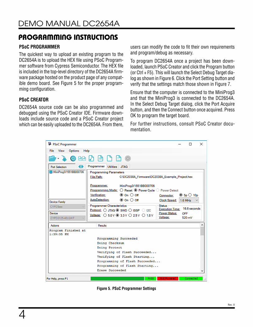
PSoC PROGRAMMER The quickest way to upload an existing program to the DC2654A is to upload the HEX file using PSoC Program-mer software from Cypress Semiconductor. The HEX file is included in the top-level directory of the DC2654A firm-ware package hosted on the product page of any compat-ible demo board. See Figure 5 for the proper program-ming configuration.
PSoC CREATORDC2654A source code can be also programmed and debugged using the PSoC Creator IDE. Firmware down-loads include source code and a PSoC Creator project which can be easily uploaded to the DC2654A. From there,
users can modify the code to fit their own requirements and program/debug as necessary.
To program DC2654A once a project has been down-loaded, launch PSoC Creator and click the Program button (or Ctrl + F5). This will launch the Select Debug Target dia-log as shown in Figure 6. Click the Port Setting button and verify that the settings match those shown in Figure 7.
Ensure that the computer is connected to the MiniProg3 and that the MiniProg3 is connected to the DC2654A. In the Select Debug Target dialog, click the Port Acquire button, and then the Connect button once acquired. Press OK to program the target board.
For further instructions, consult PSoC Creator docu-mentation.
Figure 5. PSoC Programmer Settings
4
DEMO MANUAL DC2654A
Rev. 0
PROGRAMMING INSTRUCTIONS
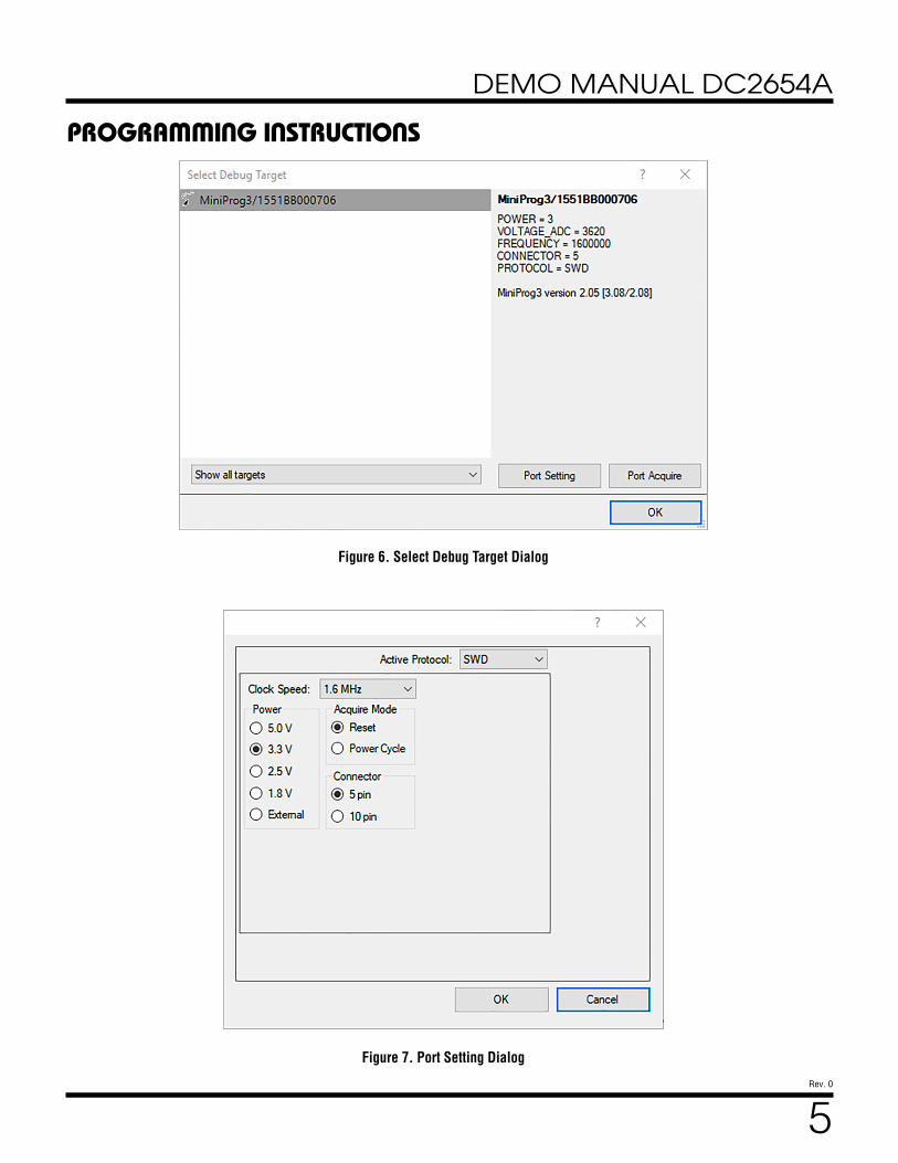
Figure 6. Select Debug Target Dialog
Figure 7. Port Setting Dialog
5
DEMO MANUAL DC2654A
Rev. 0
PROGRAMMING INSTRUCTIONS
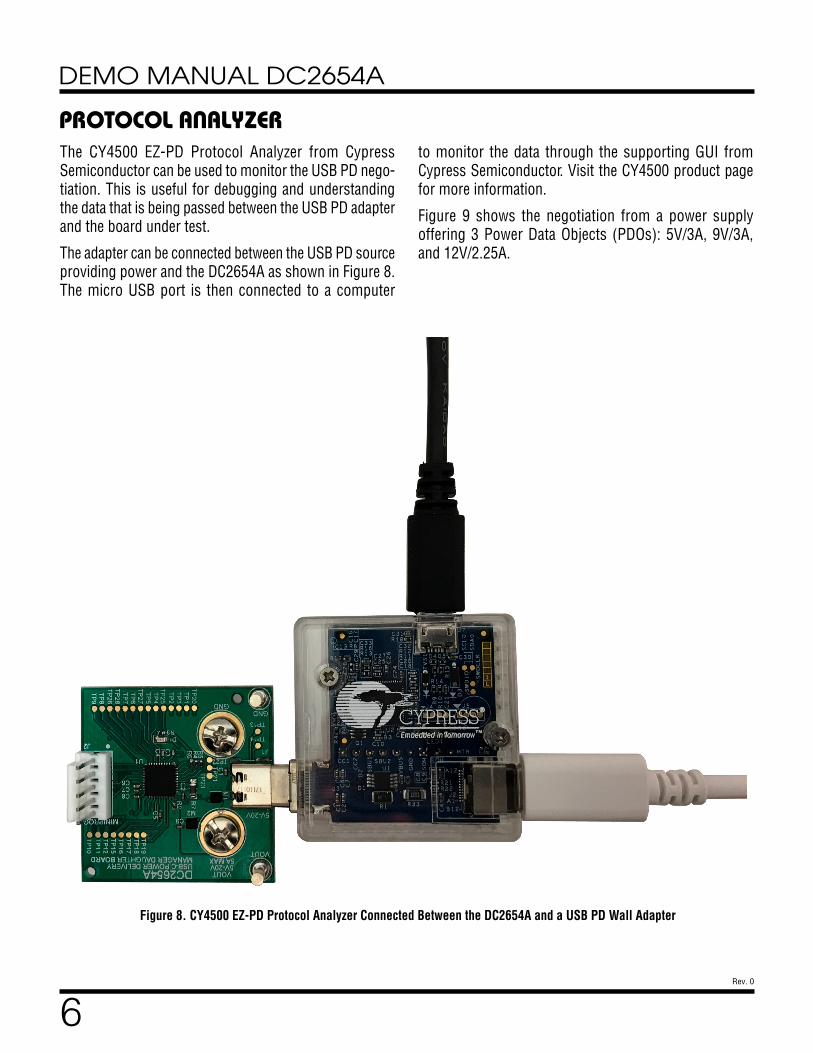
Figure 8. CY4500 EZ-PD Protocol Analyzer Connected Between the DC2654A and a USB PD Wall Adapter
6
DEMO MANUAL DC2654A
Rev. 0
PROTOCOL ANALYZERThe CY4500 EZ-PD Protocol Analyzer from Cypress Semiconductor can be used to monitor the USB PD nego-tiation. This is useful for debugging and understanding the data that is being passed between the USB PD adapter and the board under test.
The adapter can be connected between the USB PD source providing power and the DC2654A as shown in Figure 8. The micro USB port is then connected to a computer
to monitor the data through the supporting GUI from Cypress Semiconductor. Visit the CY4500 product page for more information.
Figure 9 shows the negotiation from a power supply offering 3 Power Data Objects (PDOs): 5V/3A, 9V/3A, and 12V/2.25A.
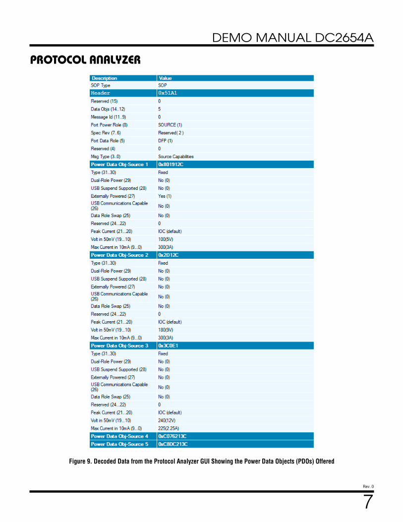
Figure 9. Decoded Data from the Protocol Analyzer GUI Showing the Power Data Objects (PDOs) Offered
7
DEMO MANUAL DC2654A
Rev. 0
PROTOCOL ANALYZER

8
DEMO MANUAL DC2654A
Rev. 0
PARTS LISTITEM QTY REFERENCE PART DESCRIPTION MANUFACTURER/PART NUMBER
Required Circuit Components
1 3 C1, C2, C9 CAP., 1µF, X5R, 35V, 10%, 0402 MURATA, GRM155R6YA105KE11D
2 2 C3, C4 CAP., 390pF, COG, 50V, 5%, 0402 AVX, 04025A391JAT2A
3 1 C5 CAP., 0.1µF, X7R, 25V, 10%, 0402 AVX, 04023C104KAT2A
4 3 C6-C8 CAP., 2.2µF, X5R, 6.3V, 10%, 0402 AVX, 04026D225KAT2A
5 1 D1 LED,GREEN, WATER CLEAR, 0603 LITE-ON, LTST-C190KGKT
6 2 M1, M2 XSTR., MOSFET N-CH, 30V, 15A, UDFN-B EP TOSHIBA, SSM6K513NU,LF
7 2 M3, M4 XSTR., MOSFET, DUAL N-CH, 0.28A, SOT-563 DIODES INC., 2N7002VAC-7
8 2 R1, R2 RES., 10MΩ, 5%, 1/16W ,0402 VISHAY, CRCW040210M0JNED
9 1 R3 RES., 1k, 1%, 1/16W, 0402, AEC-Q200 VISHAY, CRCW04021K00FKED
10 2 R4, R5 RES., 10k, 1%, 1/16W, 0402 SAMSUNG, RC1005F103CS
11 1 R6 RES., 100k, 1%, 1/10W, 0402, AEC-Q200 KOA SPEER, RK73H1ETTP1003F
12 1 R7 RES.,200Ω, 5%, 1/2W, 0805, AEC-Q200 PANASONIC, ERJP06J201V
13 1 U1 IC, USB TYPE-C PORT CONTROLLER, 40-PIN QFN CYPRESS, CYPD3125-40LQXIT
Hardware
1 2 E1, E2 TEST POINT, TURRET, 0.094" MTG. HOLE, PCB 0.062" THICK MILL-MAX, 2501-2-00-80-00-00-07-0
2 2 E3, E4 CONN., PLUG BANANA, MALE,INTERNAL THREAD KEYSTONE, 6072
3 1 J1 CONN., USB 3.1, RCPT, 24POS, 0.5mm, SMD RA MOLEX, 1054500101
4 1 J2 CONN., HEADER, MALE PIN, 5 POS, 2.54mm, ST THT TE CONNECTIVITY, 640456-5
5 1 J3 CONN., HEADER, MALE, 16 POS, 1.27mm, VERT TALL SAMTEC, FW-08-05-L-D-315-100

9
DEMO MANUAL DC2654A
Rev. 0
Information furnished by Analog Devices is believed to be accurate and reliable. However, no responsibility is assumed by Analog Devices for its use, nor for any infringements of patents or other rights of third parties that may result from its use. Specifications subject to change without notice. No license is granted by implication or otherwise under any patent or patent rights of Analog Devices.
SCHEMATIC DIAGRAM5 5
4 4
3 3
2 2
1 1
DD
CC
BB
AA
REVI
SION
HIS
TORY
ECO
REV
DESC
RIPT
ION
APPR
OVED
DATE
-03
PROD
UCTI
ONZP
06-0
4-19
USB-
C PO
WER
DEL
IVER
Y MA
NAGE
R DA
UGHT
ER B
OARD
GND
PCA
ADDI
TION
AL P
ARTS
5V-2
0V
MINI
PROG
5V-2
0V, 5
A MA
X
OPT
OPT
10M
10M
VOUT
V3P3
V3P3
V3P3
V3P3
V3P3
V3P3
VOUT
DATE
:
IC N
O.
SHEE
TOF
TITL
E: D
EMO
CIRC
UIT
SCHE
MAT
IC,
APPR
OVAL
SPC
B DE
S.
APP
ENG.
CUST
OMER
NOT
ICE
LINE
AR T
ECHN
OLOG
Y HA
S MA
DE A
BES
T EF
FORT
TO
DESI
GN A
CIRC
UIT
THAT
MEE
TS C
USTO
MER-
SUPP
LIED
SPE
CIFI
CATI
ONS;
HOW
EVER
, IT R
EMAI
NS T
HE C
USTO
MER'
S RE
SPON
SIBI
LITY
TO
VERI
FY P
ROPE
R AN
D RE
LIAB
LE O
PERA
TION
IN T
HE A
CTUA
LAP
PLIC
ATIO
N. C
OMPO
NENT
SUB
STIT
UTIO
N AN
D PR
INTE
DCI
RCUI
T BO
ARD
LAYO
UT M
AY S
IGNI
FICA
NTLY
AFF
ECT
CIRC
UIT
PERF
ORMA
NCE
OR R
ELIA
BILI
TY. C
ONTA
CT L
INEA
RTE
CHNO
LOGY
APP
LICA
TION
S EN
GINE
ERIN
G FO
R AS
SIST
ANCE
.
THIS
CIR
CUIT
IS P
ROPR
IETA
RY T
O LI
NEAR
TEC
HNOL
OGY
AND
SUPP
LIED
FOR
USE
WIT
H LI
NEAR
TEC
HNOL
OGY
PART
S.SC
ALE
= NON
ESI
ZE: N
/ASKU
NO.
SCHE
MAT
IC N
O. A
ND R
EVIS
ION:
PCA
BOM:
PCA
ASS'
Y:
www.
linea
r.com
Phon
e: (4
08)4
32-1
900
www.
analo
g.com
11
NC ZP
N/A
DC2654A
710-DC2654A_REV03
705-
DC26
54A_
REV0
3Tu
esda
y, Ju
ne 04
, 201
9
700-
DC26
54A_
REV0
3
C2 1uF
35V
C6 2.2uF
6.3V
TP23
TP7
E1
TP19
TP17
R3 1k
J21 32 4 5
TP9
M3A
2N70
02VA
C-7
TP29
R6 100k
U1
CYPD
3125
-40L
QXIT
VB
US
_P_C
TRL1
1
VB
US
_P_C
TRL0
2
CC
23
V5V
4
CC
15
VC
ON
N6
P1.
07
P1.
18
P1.
29
P1.
310
VBUS_P40
OC39
P3.638
P3.537
P3.436
P3.335
P3.234
VSS33
VBUS_DISCH32
VBUS31
41VSS
VB
US
_C_C
TRL0
30
VB
US
_C_C
TRL1
29
P0.
128
P0.
027
XR
ES
26
P2.
625
P2.
524
P2.
423
D-
22
D+
21
AUX_P / P1.611
SBU1 / P1.412
SBU2 / P1.513
AUX_N / P1.714
P2.015
P2.116
VDDD17
VDDIO18
VCCD19
VSYS20
TP1
LB1
LABE
L
M4B
2N70
02VA
C-7
R5 10k
E4
M2
SSM6
K513
NU
PCB1
PCB,
DC26
54A
REV0
3
C5 0.1uF
25V
TP18
M1
SSM6
K513
NU
TP11
R7 200 5%
1/2W
0805
TP22
TP5
E2
TP8
R2 10M
C339
0pF
TP2
TP26
C4 390p
F
C1 1uF
35V
M4A
2N70
02VA
C-7
D1 GREE
N
C8 2.2uF
6.3V
TP28
TP15
R8 OPT
M3B
2N70
02VA
C-7
TP13
R1 10M
C9 1uF
35V
TP25
M5
SSM6
K513
NU
TP24
J3
FW-0
8-05
-L-D
-315
-100
12
34
56
78
910
1112
1314
1516
TP21
STNC
L1TO
OL, S
TENC
IL, 7
00-D
C265
4ARE
V03
TP12
C7 2.2uF
6.3V
TP6
R9 OPT
J1 USB3
.1
GN
DB
12
RX
1+B
11
RX
1-B
10
VB
US
B9
SB
U2
B8
D-
B7
D+
B6
CC
2B
5
VB
US
B4
TX2-
B3
TX2+
B2
GN
DB
1
VB
US
A9
RX
2-A
10
RX
2+A
11
VB
US
A4
SB
U1
A8
D-
A7
D+
A6
CC
1A
5
GN
DA
12
TX1-
A3
TX1+
A2
GN
DA
1
GNDX1
GNDX2
GNDX3
GNDX4
E3
TP16
TP3
R4 10k
R10
OPT
0612
TP14
TP10
M6
SSM6
K513
NU
TP27
TP20
TP4
SCL
CC2
D- D+D+ D-
D+D-
CC1
RESE
T
V3P3SDA
RESE
T
CC1
P1.2
P1.0
P1.3
P1.1
P1.6
P1.5P1.7
P1.4
SMBA
LERT
SCL
P1.1
P1.0
P1.3
P1.2
P1.6
P1.4
P1.5
P1.7
SDA
CC2
SMBALERT
VOUT
10
DEMO MANUAL DC2654A
Rev. 0
ANALOG DEVICES, INC. 2020
12/20www.analog.com
ESD Caution ESD (electrostatic discharge) sensitive device. Charged devices and circuit boards can discharge without detection. Although this product features patented or proprietary protection circuitry, damage may occur on devices subjected to high energy ESD. Therefore, proper ESD precautions should be taken to avoid performance degradation or loss of functionality.
Legal Terms and Conditions By using the evaluation board discussed herein (together with any tools, components documentation or support materials, the “Evaluation Board”), you are agreeing to be bound by the terms and conditions set forth below (“Agreement”) unless you have purchased the Evaluation Board, in which case the Analog Devices Standard Terms and Conditions of Sale shall govern. Do not use the Evaluation Board until you have read and agreed to the Agreement. Your use of the Evaluation Board shall signify your acceptance of the Agreement. This Agreement is made by and between you (“Customer”) and Analog Devices, Inc. (“ADI”), with its principal place of business at One Technology Way, Norwood, MA 02062, USA. Subject to the terms and conditions of the Agreement, ADI hereby grants to Customer a free, limited, personal, temporary, non-exclusive, non-sublicensable, non-transferable license to use the Evaluation Board FOR EVALUATION PURPOSES ONLY. Customer understands and agrees that the Evaluation Board is provided for the sole and exclusive purpose referenced above, and agrees not to use the Evaluation Board for any other purpose. Furthermore, the license granted is expressly made subject to the following additional limitations: Customer shall not (i) rent, lease, display, sell, transfer, assign, sublicense, or distribute the Evaluation Board; and (ii) permit any Third Party to access the Evaluation Board. As used herein, the term “Third Party” includes any entity other than ADI, Customer, their employees, affiliates and in-house consultants. The Evaluation Board is NOT sold to Customer; all rights not expressly granted herein, including ownership of the Evaluation Board, are reserved by ADI. CONFIDENTIALITY. This Agreement and the Evaluation Board shall all be considered the confidential and proprietary information of ADI. Customer may not disclose or transfer any portion of the Evaluation Board to any other party for any reason. Upon discontinuation of use of the Evaluation Board or termination of this Agreement, Customer agrees to promptly return the Evaluation Board to ADI. ADDITIONAL RESTRICTIONS. Customer may not disassemble, decompile or reverse engineer chips on the Evaluation Board. Customer shall inform ADI of any occurred damages or any modifications or alterations it makes to the Evaluation Board, including but not limited to soldering or any other activity that affects the material content of the Evaluation Board. Modifications to the Evaluation Board must comply with applicable law, including but not limited to the RoHS Directive. TERMINATION. ADI may terminate this Agreement at any time upon giving written notice to Customer. Customer agrees to return to ADI the Evaluation Board at that time. LIMITATION OF LIABILITY. THE EVALUATION BOARD PROVIDED HEREUNDER IS PROVIDED “AS IS” AND ADI MAKES NO WARRANTIES OR REPRESENTATIONS OF ANY KIND WITH RESPECT TO IT. ADI SPECIFICALLY DISCLAIMS ANY REPRESENTATIONS, ENDORSEMENTS, GUARANTEES, OR WARRANTIES, EXPRESS OR IMPLIED, RELATED TO THE EVALUATION BOARD INCLUDING, BUT NOT LIMITED TO, THE IMPLIED WARRANTY OF MERCHANTABILITY, TITLE, FITNESS FOR A PARTICULAR PURPOSE OR NONINFRINGEMENT OF INTELLECTUAL PROPERTY RIGHTS. IN NO EVENT WILL ADI AND ITS LICENSORS BE LIABLE FOR ANY INCIDENTAL, SPECIAL, INDIRECT, OR CONSEQUENTIAL DAMAGES RESULTING FROM CUSTOMER’S POSSESSION OR USE OF THE EVALUATION BOARD, INCLUDING BUT NOT LIMITED TO LOST PROFITS, DELAY COSTS, LABOR COSTS OR LOSS OF GOODWILL. ADI’S TOTAL LIABILITY FROM ANY AND ALL CAUSES SHALL BE LIMITED TO THE AMOUNT OF ONE HUNDRED US DOLLARS ($100.00). EXPORT. Customer agrees that it will not directly or indirectly export the Evaluation Board to another country, and that it will comply with all applicable United States federal laws and regulations relating to exports. GOVERNING LAW. This Agreement shall be governed by and construed in accordance with the substantive laws of the Commonwealth of Massachusetts (excluding conflict of law rules). Any legal action regarding this Agreement will be heard in the state or federal courts having jurisdiction in Suffolk County, Massachusetts, and Customer hereby submits to the personal jurisdiction and venue of such courts. The United Nations Convention on Contracts for the International Sale of Goods shall not apply to this Agreement and is expressly disclaimed.