Embed Size (px)
Citation preview
Page 1 of 30
Delong's Fan Club: Designing a Cost-
Efficient Programmable Multi Effects
Pedal For Electric Guitar
Jack Galletta, Sunny Hwang, and Yaman Shrestha
12/10/2020
Capstone Design ECE 4440 / ECE4991 Technical Advisor: Harry Powell
Signatures
Page 2 of 30
Statement of work:
Jack Galletta:
The main contributions I made to the project consisted of the preliminary analysis done to
calculate specifications for our project, as well as some of the design decisions and calculations
done in regards to the effects themselves. First, in order to even decide on what microcontroller
to use, I created a spectral analysis of a typical guitar signal, in order to ensure that the specs for
our controller would be able to sample the signal at a rate high enough to retain the information
contained in the original signal. Understanding the frequency response of the guitar signal is a
key part of processing the signal and producing effects, so this was a crucial step required to
move our project along. In order to perform the spectral analysis, the electric guitar was plugged
into a USB Audio CODEC interface and Audacity was used to record and analyze the sound.
The same E minor pentatonic scale sample was recorded through 85/15 humbucker pickups on a
PRS guitar at two different sample rates, 44.1kHz and 8kHz.
The two plots gave us a lot of insight into the guitar’s sound signal, and allowed us to
draw some important conclusions for our design. Firstly, we saw from both plots that the
frequency of the signal was never exceeding about 8kHz, and even then, the magnitude of the
frequencies are too small to even be picked up by the amplifier, down to about 4kHz. From this
we can determine that a minimum sampling rate of 8kHz would be required, since it is twice the
max frequency, however the group decided that sampling at twice that rate, 16kHz, would be a
more ideal rate in order to preserve any additional harmonics and overtones that might occur. By
choosing a 16kHz sampling rate for our design, we needed to ensure that our selected embedded
controller would have a powerful enough ADC unit to sample at this frequency.
In addition to this work with sampling, I was responsible for the creation of the Ultiboard
final layout, the assembly of the physical pedal itself, and lastly, playing the guitar in order to
test our final project.
Sunny Hwang:
The work that I completed for the project consisted of the hardware design for the
system. The PCB design consisted of a power stage, an input stage, and an output stage. These
stages were created and tested using multisim and additional components that were created were
made with Ultiboard. Furthermore, the schematics that I created for the PCB were necessary to
filter out the signal before and after analog to digital and digital to analog conversions. This is
important for the project since there is a lot of noise that is introduced to the input signal that is
superfluous and may lead to undesirable results especially when doing ADC and DAC
conversions.
Given a calculated cutoff frequency, I made design decisions on components to create the
desired filter. With the audacity analysis, a design decision was made to create a second order
filter since the cutoff frequency and rolloff would match the spectrum nicely. Knowing that a
Page 3 of 30
second order filter was needed, calculations for the resistors and capacitors were done such that
the quality factor was 0.707 while also meeting the cutoff frequency.
Yaman Shrestha:
One of the contributions that I made to the project consists of ensuring that the design
choice of the microcontroller is sufficient to sample the guitar audio signal and also perform the
necessary algorithms to create the desired effects. Based on the requirements for the, I researched
and decided to pick the MSP432P401R launchpad microcontroller. The MSP432P401R has a
Arm® 32-bit Cortex® M4F CPU with floating-point unit and memory protection unit which has
a 48 MHz clock. More importantly, the SAR analog-to-digital converter (ADC) has 16-bit
precision and up to 1 Msps (Million samples per seconds). This means that the microcontroller has
the capability to sample at 1MHz per second, which was more than sufficient for the project.
Finally the SRAM capacity of this controller was 64 kB which is more than sufficient to store the
delay and perform extra storing operations.
Another important contribution I had for the project was developing the code for
microcontroller. I was responsible for initializing all the electronic components that were used
alongside with the MSP432P401R microcontroller, including the ADC and DAC. Once ensuring
these were initialized properly, I then ensured that signal data was transferred correctly and
properly from one stage to another using SPI. Afterward, I worked closely with Jack on
programming the effects.
Page 4 of 30
Table of Contents
Capstone Design ECE 4440 / ECE4991 1
Signatures 1
Statement of work 2
Table of Contents 4
Table of Figures 5
Abstract 6
Background 6
Design Constraints 7
External Standards 7
Tools Employed 7
Ethical, Social, and Economic Concerns 8
Intellectual Property Issues 10
Detailed Technical Description of Project 11
Electrical Design 12
Board Layouts 16
Coding 18
Project Timeline 19
Test Plan 21
Final Results 22
Costs 25
Future Work 26
References 27
Appendix 30

Page 5 of 30
Table of Figures Figure 1 General Block Diagram of the different stages of the device 11
Figure 2 The full Multisim system schematic 12
Figure 3 Power stage schematic 12
Figure 4 Input stage schematic 13
Figure 5 Audacity frequency spectrum from a guitar 14
Figure 6 Output stage schematic 15
Figure 7 First Board Layout 16
Figure 8 Second board layout 17
Figure 9 Initial Gantt Chart 19
Figure 10 Final Gantt Chart 19
Figure 11 PCB Test Plan 21
Figure 12 Final PCB with all components 23
Figure 13 Final Pedal Fully Wired 23
Figure 14 Setup Used for Testing 24
Figure 15 Spreadsheet of purchases and budget 30
Page 6 of 30
Abstract
The Multi-effect pedal is an electronic unit for an electric guitar that can be programmed to add a
multitude of different sounds and effects. The unit will take in an analog signal from a guitar,
pass it into an embedded board, and perform various digital signal processing (DSP) operations
to produce the desired effect. In order to process the signal from the guitar, we included an input
filtering stage to filter out frequencies above a calculated frequency. Once filtered, we pass the
filtered signal to an ADC to convert the analog guitar signal into a digital wave that can be
processed by the embedded chip in the microcontroller. The MSP432P401R chip we will use in
this project processes this digital signal and performs the required DSP operations to create the
desired effect. The modified digital signal will then go through an DAC to output the modified
analog signal, which will be played on an amp.
Background Guitar pedals are an essential component to a player’s sound and what kind of music they
produce. By being able to modify the input wave from an electric guitar, pedals can produce a
wide array of sounds and effects through the electrical components inside. While current pedals
are a great way to improve your sound, multiple limitations arise when chaining multiple effects
together, and is the reason behind the creation of this project [1]. Firstly, pedals are typically
engineered to produce a single effect. This is great for specific features, as the electronics are
typically simple and can produce a good result, but having to get a different pedal for every kind
of effect becomes not only expensive, but tedious to carry around and causes competition for
space on a guitar player’s pedalboard. A second drawback to single effect guitar pedals is the
chaining of effects that occurs. When a signal is run through multiple pedals, regardless of
whether they are on or off, the signal will have loss as it travels through the circuitry of some of
the pedals [2]. By eliminating the chaining of multiple pedals with our “all-in-one" effects unit,
we can eliminate the loss of input signal that occurs leading to a cleaner and more robust sound.
While multi-effects guitar pedal units do exist, one of the largest barriers to these units is cost.
The industry standard, the Line 6 Helix Multi Effects Board, runs around $1700 [3]. While this
unit includes some special features, such as the ability to save different pedal profiles and over
70 different effects, the core value of the product lies in the ability to use a single pedal to
produce a multitude of effects. The importance of our project is the ability to recreate a similar
unit at a much lower cost, while still being able to accomplish the same core features.
This project will lean heavily on previous coursework and experience from both the embedded
and FUN series of classes. Since the first stage of the project will involve designing and
prototyping our circuit, our design experience from FUN will prove valuable in calculating the
correct values for our electronic components. Additionally, Multisim and Ultiboard will be used
for the final header board design, skills we also have learned throughout the FUN series. In
order to create the actual effects for the guitar signal, our DSP and coding experience will be
used to program the effects onto the MSP432P401R board, drawing from our Embedded
Systems experience.
Page 7 of 30
Constraints
Design Constraints
There were constraints set by the microcontrollers limitations. The SRAM capacity of the MSP432
microcontroller is 64 kB so in order for a delay effect to work it has to use less memory than 64
kB. Also, the microcontroller can sample at 1MHz per second so the input signal sampling has to
be under those limitations.
Some other constraints came from the encouragement of buying parts at Digikey[4] distributed as
cut-tape packaging. Another constraint that comes from ordering through Digikey is the desired
part has to be in stock or else it won’t be shipped in time.
A manufacturing constraint that arose came from needing a precise machine to solder on small
parts that the hand is incapable of doing. Because of this, the board had to be sent to WWW
electronics [5] so the time needed to travel to WWW as well as the time for them to stuff the board
had to be taken into account.
A software availability constraint can come from not having a multisim, ultiboard, or LabView
license. UVA provides the license but if the license needed to be renewed and work had to be done
before a certain date, then there would be a problem if the software access code wasn’t readily
attainable.
Economic and Cost Constraints
This semester there was a budget of $250 which is half the usual budget of $500 that ECE/CPE
Capstone groups usually receive. Because of this, it was very important to make sure that all the
necessary components were obtainable within the $250 threshold. Furthermore, we planned to
create a cost effective alternative to premium multi-effects pedals so the components bought
were affordable and the creation of the system was well under the $1000 premium price range.
External Standards 1. The enclosure for the electrical components will meet NEMA type 1 standards [6]:
i. Protects against dust but NOT dust tight ii. Protects against indirect splashing and light
iii. Primarily used to protect against contact with live electrical components
iv. For use indoors and normal atmospheric conditions
2. The PCB board will follow IPC standards for it’s spacing and traces when being
manufactured [7]
Tools Employed ● Multisim [8]:
○ Multisim was used to design the PCB schematic and test out if each stage
functions correctly. This tool was very important in establishing the final
schematic design since there are only 2 chances to print the board throughout the
semester. Without Multisim and its tests, it would be hard to determine if a design

Page 8 of 30
would work properly thus printing out a functional board within 2 tries would
have been difficult. Prior skills learned from fundamentals of electrical
engineering I,II, and III had to be referenced in order to remember how to do
certain tests such as the transient analysis and ac sweep.
● Ultiboard [9]:
○ Ultiboard was used to create the PCB board blueprint as well as create additional
components that aren’t included in the Multisim library. This tool can also
interface with Multisim allowing seamless use when transfering the multisim
schematic to Ultiboard. Also, when creating the blueprint for the PCB, Ultiboard
allows the user to place the components in the desired spot as well as route the
wire as desired. This was important for when the 2 female 2x10 pins needed to be
placed a specific distance apart to ensure that the PCB can mount the MSP432.
The part wizard was another necessary contribution that Ultiboard had, but it had
to be learned since no prior coursework touched it. Using the part wizard, the
DAC was built and uploaded to the Multisim library.
● Virtual Bench [10]:
○ This tool was used after the printing and stuffing of the PCB to ensure that the
board functions properly. Various tests are done to see if the power supply is
supplying the correct power, if the input signal successfully reaches the
microcontroller, and other voltage and signal tests. This is important to help
ensure that the PCB performs its intended task before connecting it to the
microcontroller or guitar such that accidents are avoided.
● Code Composer (C/C++) [11]:
○ Code Composer Studio is an integrated development environment to develop
applications for Texas Instruments embedded processors. For our project we used
it to program the MSP432P401R microcontroller in C. This was the platform that
initialized all the components connected to the microcontroller, such as the DAC
and ADC through code. In order to communicate data between these components,
we coded the SPI protocol. Finally, the effects were coded in using this platform.
The debugger tool in Code Composer was extremely useful in debugging the code
and seeing the various states of the audio signal digitally.
Ethical, Social, and Economic Concerns
Environmental Impact
In terms of environmental impact, the power supply causes the main concern. The wall
plug-in power supply will use electricity produced by power plants which in most cases use
fossil fuels to supply the electricity. The 9V power supply, overtime, will contribute to carbon
emissions caused by using fossil fuels. Furthermore, if the power supply is not disposed of
properly it can lead to groundwater pollution if discarded into a landfill. The best way to avoid
adverse effects from improper disposal is to send the power supply to be recycled at a recycling
center.
Page 9 of 30
Sustainability
This project presents a design that is more sustainable than previous designs by
implementing a plug-in power supply such that the lifespan is longer. The lifetime of the plug-in
power supply will last longer than if there was a battery power supply since it wouldn’t need to
be replaced every so often. This project is relatively scalable since the coded effects can be
placed into an open library for other users to download and use at their leisure. Furthermore,
because the goal of this project is to make a multi-effects pedal, this will reduce the necessity of
buying multiple effects pedals.
Health and Safety
The system can be easily reproduced. The PCB is the only part that needs to be
manufactured. All the connectors and electrical components will be off-the-shelf as well as the 9-
volt power supply. All the parts will be readily available for mass assembly and
manufacturability in the future. There are no resistors, capacitors, power supplies, etc. that are
restricted for purchase in reproducing this multi-effect pedal.
Manufacturability
The system can be easily reproduced. The PCB is the only part that needs to be
manufactured. All the connectors and electrical components will be off-the-shelf as well as the 9-
volt power supply. All the parts will be readily available for mass assembly and
manufacturability in the future. There are no resistors, capacitors, power supplies, etc. that are
restricted for purchase in reproducing this multi-effect pedal.
Ethical Issues
The ethical issue that will arise when creating a multi-effects guitar pedal is that there is a
big library of guitar effects that can be easily taken and modified to be our own. Plagiarism of
effects can be easily done when any effect can be copied and coded onto a multi-effects pedal. In
addition to plagiarism, piracy is another ethical issue that may arise. Producers and artists that
utilize our device might come across their work distributed without their consent, which is often
true for most digitized music. In fact, piracy due to digitized music has led to economic losses
around 12.5 billion dollars every year according to the Recording Rights Association of
America.

Page 10 of 30
Intellectual Property Issues
This project is not patentable due to the following patents that have claims that cover the material
covering the full scope of our project.
Patent 1: US8957297B2 [12]
This patent covers the primary purpose and functionality of our projects with an independent
claim (claim 1) for “a programmable pedalboard for a musical instrument, the pedalboard
comprising: a docking station for receiving a removable portable computer that provides a
plurality of instrument effects, the docking station being configured to, receive an audio signal
from a musical instrument and modify the audio signal from the musical instrument based on at
least one instrument effect from the plurality of instrument effects.” In addition, this patent
covered additional features we didn't include such as the pedal board being able to wirelessly
transmit data of the modified signal to a portable computer.
Patent 2: US20060278068 [13]
This patent is the patent for the original electric guitar pedal. In general, this patent entirely
covers the pedal portion of our project. The dependent claim 8 which states “Sound controller
system according to claim 1, wherein at least one of said at least one distance representing signal
is an analogue signal and at least one of said at least one control signal is a digital signal,” is very
similar to how our system takes in the analog audio signal and later converts it digitally to apply
effects. Unlike this patent, we are programmatically adding effects.
Patent 3: GB2456307 [14]
This patent covers the digital effects creation aspect of our project with an independent claim
(claim 1) for “providing digital control for analogue effects devices”. This patent incorporates a
digital control aspect to an analog guitar pedal. This is slightly different from our project as it is
more aimed towards the control (on/off function) for an effects pedal but it still aims to provide
the digital aspect into a guitar pedal as we aimed to do.
Page 11 of 30
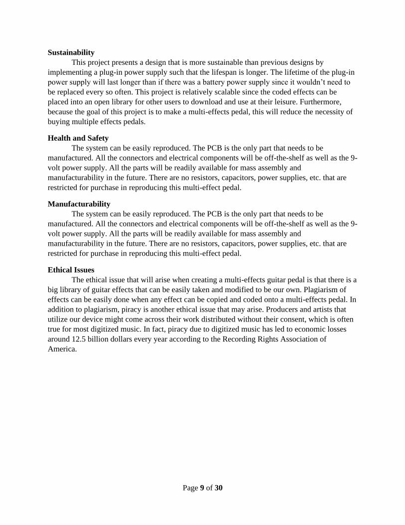
Detailed Technical Description of Project
The Multi-effect pedal is an attachable electronic unit that can be connected to an electric
guitar to add a variety of customizable and programmable effects. This device gives the user the
freedom to add a multitude of effects to their electric guitar signal chain for fast tone
customization. By placing the pedal in between the guitar and amplifier in the signal chain, the
user will be able to activate a footswitch on the pedal to turn the programmed effects on and off.
The pedal unit will also feature a potentiometer that controls input impedance to the pedal,
allowing for more accurate dialing of the desired tone. Additionally, a future vision for the
project is to attempt to create a small library of effects to choose from, so that the user is able to
load different effects on the pedal quickly. The device uses an MSP432P401R board for signal
processing in conjunction with a custom-built header board that handles the signal before and
after it passes through the embedded controller
Figure 1 General Block Diagram of the different stages of the device
Page 12 of 30
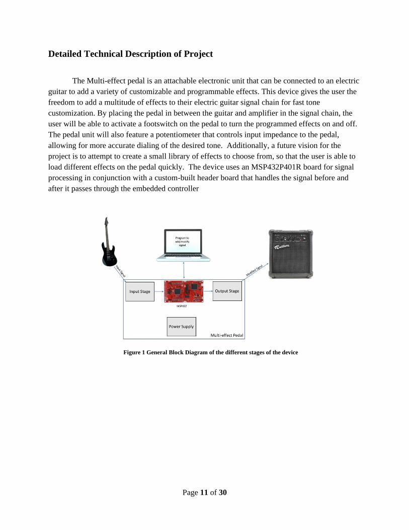
Electrical Design
Figure 2 The full Multisim system schematic
The Multi-effect pedal can be broken down into 4 distinct stages:the power stage, the input stage,
MSP432P401R board, and the output stage, as can be seen in the diagram above. The breakdown
of each stage and the design choices that were made are in the following sections below.
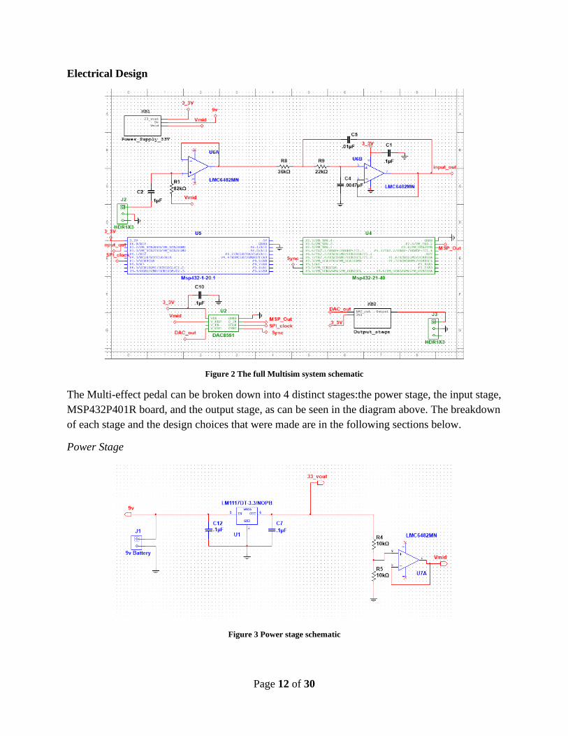
Power Stage
Figure 3 Power stage schematic
Page 13 of 30
The main purpose of the power stage is to power all the various components of the board with
their respective voltages. Within this stage, a 9-V power supply is used [15] for power, a 3.3 V
voltage regulator is used to step down the 9 V power to provide 3.3 V (necessary to power the
microcontroller), [16] 2 ceramic bypass capacitors [17] are used to remove AC voltage for the
voltage regulator, 2 resistors [18] are used to voltage divide the 3.3 V to create a V-mid voltage,
and a LMC6482 operational amplifier [19] is used to provide a unity gain buffer for V-mid.
Various design decisions were made when creating the power supply. First and foremost, it was
necessary to figure out which voltages we needed to power components that required power. It
was found that the microcontroller needed 3.3 V for power and the Op-Amps needed a voltage in
the range of 3V - 15.5V. Furthermore, a V-mid value was necessary to center the input signal
such that its voltage is centered at 1.65 V. Without this V-mid voltage, we run the risk of frying
the microcontroller since it can only take a max voltage input of 3.3 V. So with the two voltage
requirements of 3.3V and 1.65V, the power supply stage was built to achieve those voltages.
Lastly, the design decision we made regarding the power supply has its perks but also some
tradeoffs. Instead of opting for a 9V battery, we decided to use a 9V wall power source. The
power source won’t require as many replacements as a 9V battery would albeit the tradeoff was
the pedal would have to have a wall outlet available to use. The 9V battery on the other hand
would be more portable since it doesn’t require an outlet.
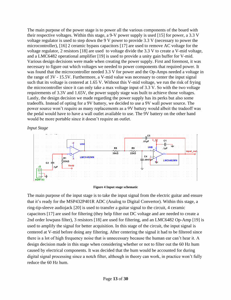
Input Stage
Figure 4 Input stage schematic
The main purpose of the input stage is to take the input signal from the electric guitar and ensure
that it’s ready for the MSP432P401R ADC (Analog to Digital Convertor). Within this stage, a
ring-tip-sleeve audiojack [20] is used to transfer a guitar signal to the circuit, 4 ceramic
capacitors [17] are used for filtering (they help filter out DC voltage and are needed to create a
2nd order lowpass filter), 3 resistors [18] are used for filtering, and an LMC6482 Op-Amp [19] is
used to amplify the signal for better acquisition. In this stage of the circuit, the input signal is
centered at V-mid before doing any filtering. After centering the signal it had to be filtered since
there is a lot of high frequency noise that is unnecessary because the human ear can’t hear it. A
design decision made in this stage when considering whether or not to filter out the 60 Hz hum
caused by electrical components. It was decided that the hum would be accounted for during
digital signal processing since a notch filter, although in theory can work, in practice won’t fully
reduce the 60 Hz hum.

Page 14 of 30
Figure 5 Audacity frequency spectrum from a guitar
Lastly, the main design decision that was made in this stage was deciding which filter and cut off
frequency to use. After analyzing the guitar audacity spectrum above, it is determined that the
cutoff frequency should be at 800 Hz since that is where the spectrum starts rolling off.
Furthermore, it was decided that the filter should be a second order low pass filter since the
spectrum above falls off at a rate of 40 dB/decade. The low pass filter was chosen since we want
to eliminate higher frequencies.
MSP432P401R
The MSP432P401R board [21] is one of the most important components to our device. This
portion of the device is heavily dependent on the effects that are coded(through Code Composer)
for the MSP432P401R board to apply. Specifically, the MSP432P401R board takes the digitized
waveform from the output of its own internal ADC and performs all necessary Digital Signal
Processing (DSP) to create a desired effect. The following MSP432P401R will also come with a
MAC unit (the ARM Cortex-M4F core processor has a single cycle MAC unit [22]), which will
assist with digital signal processing. This MSP launchpad was specifically chosen since it met
many requirements. This microcontroller has an ADC that runs on 14 bits with 16 bit precision
which is sufficient for our means of signal processing. It also has a sampling rate at 1MHz per
second which is more than enough to sample a guitar signal. Next, it has 16 kB SRAM storage
which is sufficient and necessary for running a delay effect.
Page 15 of 30
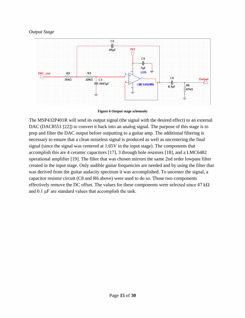
Output Stage
Figure 6 Output stage schematic
The MSP432P401R will send its output signal (the signal with the desired effect) to an external
DAC (DAC8551 [22]) to convert it back into an analog signal. The purpose of this stage is to
prep and filter the DAC output before outputting to a guitar amp. The additional filtering is
necessary to ensure that a clean noiseless signal is produced as well as uncentering the final
signal (since the signal was centered at 1.65V in the input stage). The components that
accomplish this are 4 ceramic capacitors [17], 3 through hole resistors [18], and a LMC6482
operational amplifier [19]. The filter that was chosen mirrors the same 2nd order lowpass filter
created in the input stage. Only audible guitar frequencies are needed and by using the filter that
was derived from the guitar audacity spectrum it was accomplished. To uncenter the signal, a
capacitor resistor circuit (C8 and R6 above) were used to do so. Those two components
effectively remove the DC offset. The values for these components were selected since 47 kΩ
and 0.1 μF are standard values that accomplish the task.
Page 16 of 30
Board Layouts
First Board Layout
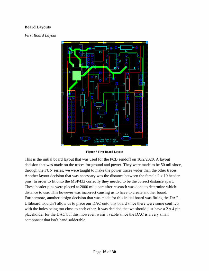
Figure 7 First Board Layout
This is the initial board layout that was used for the PCB sendoff on 10/2/2020. A layout
decision that was made on the traces for ground and power. They were made to be 50 mil since,
through the FUN series, we were taught to make the power traces wider than the other traces.
Another layout decision that was necessary was the distance between the female 2 x 10 header
pins. In order to fit onto the MSP432 correctly they needed to be the correct distance apart.
These header pins were placed at 2000 mil apart after research was done to determine which
distance to use. This however was incorrect causing us to have to create another board.
Furthermore, another design decision that was made for this initial board was fitting the DAC.
Ultiboard wouldn’t allow us to place our DAC onto this board since there were some conflicts
with the holes being too close to each other. It was decided that we should just have a 2 x 4 pin
placeholder for the DAC but this, however, wasn’t viable since the DAC is a very small
component that isn’t hand solderable.
Page 17 of 30
Second Board Layout
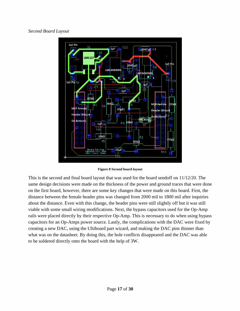
Figure 8 Second board layout
This is the second and final board layout that was used for the board sendoff on 11/12/20. The
same design decisions were made on the thickness of the power and ground traces that were done
on the first board, however, there are some key changes that were made on this board. First, the
distance between the female header pins was changed from 2000 mil to 1800 mil after inquiries
about the distance. Even with this change, the header pins were still slightly off but it was still
viable with some small wiring modifications. Next, the bypass capacitors used for the Op-Amp
rails were placed directly by their respective Op-Amp. This is necessary to do when using bypass
capacitors for an Op-Amps power source. Lastly, the complications with the DAC were fixed by
creating a new DAC, using the Ultiboard part wizard, and making the DAC pins thinner than
what was on the datasheet. By doing this, the hole conflicts disappeared and the DAC was able
to be soldered directly onto the board with the help of 3W.
Page 18 of 30
Coding
In order to program the MSP432P401, we utilized Code Composer for the IDE to simplify the
process of programming a TI product. In addition, the debugger was extremely helpful to test the
code and find bugs throughout the code. The language we used throughout the project was C.
One of the main initial tasks of the coding portion of this project was initializing all the
components of the project. This included the Timer, Clock, ADC, and DAC. This required
reading the MSP432 family documentation that went in great detail on configuring the Timer,
Clock and ADC to our specification. In order to send data from the MSP432P401R to the DAC,
we utilized the SPI protocol, which allowed us to synchronously send data.
The effects that we initially planned to complete were Distortion, Overdrive, Fuzz, and Delay.
To create the distortion effect, the circuit will have to saturate the input signal. Creating
overdrive will consist of providing a gain boost to the incoming wave, creating a dynamic
distortion-like effect [23]. In order to create the fuzz effect, the incoming wave will have to be
clipped at the top and bottom according to a predetermined threshold value, otherwise known as
square wave clipping [24]. In order to create the delay effect, we will store the current signal
value in the current location within a circular buffer and then retrieve the oldest value and
averaging it with the current signal [25]. In order to store and produce a good sounding delay
effect, the incoming guitar signal will be sampled at a minimum of 16kHz, which is more than
double the frequency of the highest frequency sound produced by the electric guitar.
Page 19 of 30
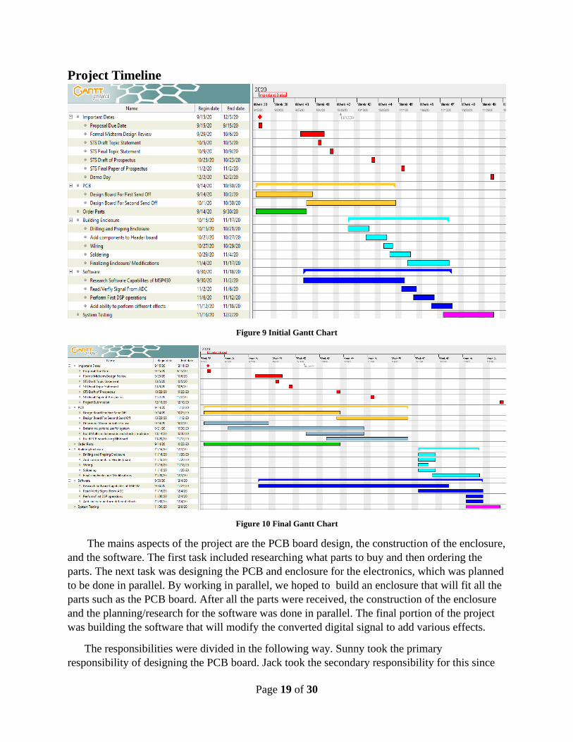
Project Timeline
Figure 9 Initial Gantt Chart
Figure 10 Final Gantt Chart
The mains aspects of the project are the PCB board design, the construction of the enclosure,
and the software. The first task included researching what parts to buy and then ordering the
parts. The next task was designing the PCB and enclosure for the electronics, which was planned
to be done in parallel. By working in parallel, we hoped to build an enclosure that will fit all the
parts such as the PCB board. After all the parts were received, the construction of the enclosure
and the planning/research for the software was done in parallel. The final portion of the project
was building the software that will modify the converted digital signal to add various effects.
The responsibilities were divided in the following way. Sunny took the primary
responsibility of designing the PCB board. Jack took the secondary responsibility for this since
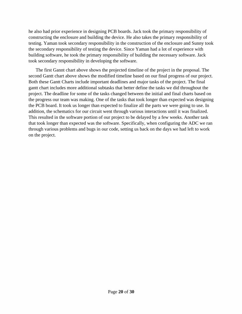
Page 20 of 30
he also had prior experience in designing PCB boards. Jack took the primary responsibility of
constructing the enclosure and building the device. He also takes the primary responsibility of
testing. Yaman took secondary responsibility in the construction of the enclosure and Sunny took
the secondary responsibility of testing the device. Since Yaman had a lot of experience with
building software, he took the primary responsibility of building the necessary software. Jack
took secondary responsibility in developing the software.
The first Gannt chart above shows the projected timeline of the project in the proposal. The
second Gantt chart above shows the modified timeline based on our final progress of our project.
Both these Gantt Charts include important deadlines and major tasks of the project. The final
gantt chart includes more additional subtasks that better define the tasks we did throughout the
project. The deadline for some of the tasks changed between the initial and final charts based on
the progress our team was making. One of the tasks that took longer than expected was designing
the PCB board. It took us longer than expected to finalize all the parts we were going to use. In
addition, the schematics for our circuit went through various interactions until it was finalized.
This resulted in the software portion of our project to be delayed by a few weeks. Another task
that took longer than expected was the software. Specifically, when configuring the ADC we ran
through various problems and bugs in our code, setting us back on the days we had left to work
on the project.

Page 21 of 30
Test Plan
Figure 11 PCB Test Plan
The initial test plan that we created for the PCB was very useful in ensuring the PCB board was
built correctly. This starts with a visual inspection of the PCB. When we obtained our first PCB,
we followed the test plan and found with a visual inspection that the header pins to connect the
PCB to the MSP were the wrong dimensions, resulting in us to rebuild the PCB board and reprint
it. After passing the visual inspection, we tested the power supply. This includes checking if the
regulator was the right orientation and had the right voltage output of 3.3 V. We came to a
problem with the output voltage of the regulator being less than 3.3 V, however by following the
test plan by checking the battery, we found that the batter was outputting less than 9V, which
was fixed with a simple replacement. After ensuring that the power supply was outputting the
proper voltage, we followed by testing the input filter. This required checking the orientation of
the om-amp and resistor values. After those checks, we tested it with a sample signal to verify
that frequencies higher than the cutoff frequency were filtered out. Once that was correct, we
then followed by testing the DAC and verifying an analog signal was outputted. Finally, we
followed the same procedure as the input stage and verified that the output filter was giving us
the desired clean signal.
Page 22 of 30
Final Results The final product met many of our design expectations that we laid out, namely the board design
and wiring diagrams, however the actual signal processing proved to be more challenging than
anticipated and we fell short on creating some of the effects.
In terms of hardware, our final circuit turned out to be very close to our initial design, with only
some slight modifications along the way to a couple resistor values and the addition of some
bypass capacitors. We also had some flaws in our initial Ultiboard design, namely with our
DAC footprint on the board being too small to solder by hand, thus resulting in an updated board
layout that accommodated the small DAC unit, which was sent to 3W to be soldered
professionally. In all, the final board was capable of taking in a sound signal, performing the
necessary filtering that took out the 60Hz buzz and the unnecessary signals above our designated
sampling rate, and sending the signal into the onboard ADC on the MSP432. One hardware
malfunction that did occur out of our control was that of our voltage converter, which resulted in
the device producing a 2.5V signal rather than the 3.3V needed to power the MSP432. To work
around this issue, the team had to hardwire the USB cable on the MSP432 to a separate power
source, in our case a laptop, in order to sufficiently power the MSP.
In our software implementation, longer than expected configuration of the MSP432
unfortunately led to the team having to cut out many of the effects that we had planned to
implement. The main time demanding task was the configuration of the ADC. According to our
Gannt chart, the initial plan was to configure the entire device in a week, but that soon became
less and less feasible as the type of signal processing that we were doing with the device had
been done very few times and was poorly documented on the internet. We had previously
researched multiple solutions to implementing the ADC for our use case prior to the project
being started, but many of the implementations we tried were unsuccessful. Eventually, the team
did get the MSP432 to process a sound signal and then pass it through to the DAC and output it
on the jack of the pedal, but the amount of time taken to implement this feature left little to no
time to work on some of our more complicated effects, such as our delay. The main effect we
were able to produce was being able to add a digital gain to the incoming signal, producing an
overdriven effect that was actually usable in guitar playing. Although not perfect, properly
dialing in the pedal as well as the amp settings resulted in the “crunchy” rock and roll sound that
we had initially planned to achieve.
This final output of the project was a fully enclosed pedal with a footswitch that was able to
process the incoming guitar signal, filter it, sample it at our desired rate, add a digital gain/drive
effect to the signal programmatically, and then output it to the amplifier. Although this did not
quite live up to our initial expectations of being able to create an entire library of effects, the
project was still extremely rewarding and served as a motivating experience from which we
could build upon in the future.
Page 23 of 30
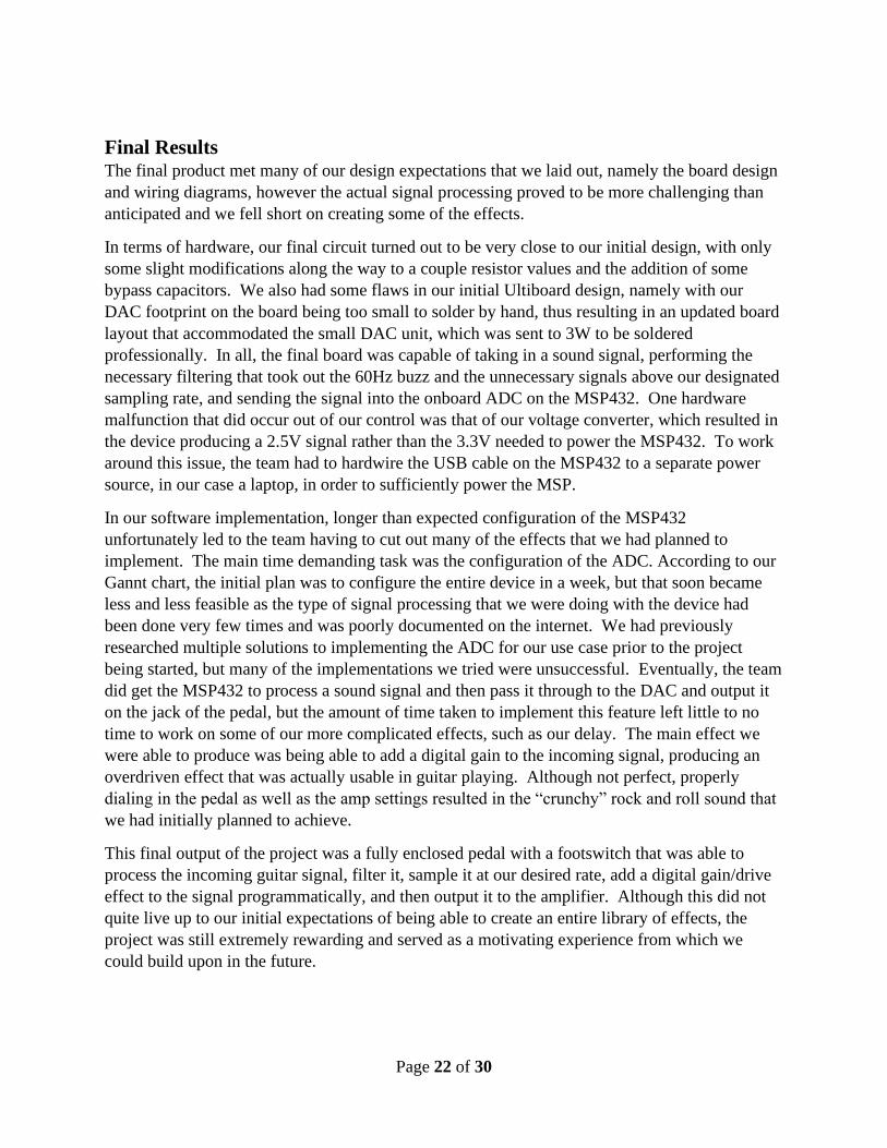
Figure 12 Final PCB with all components
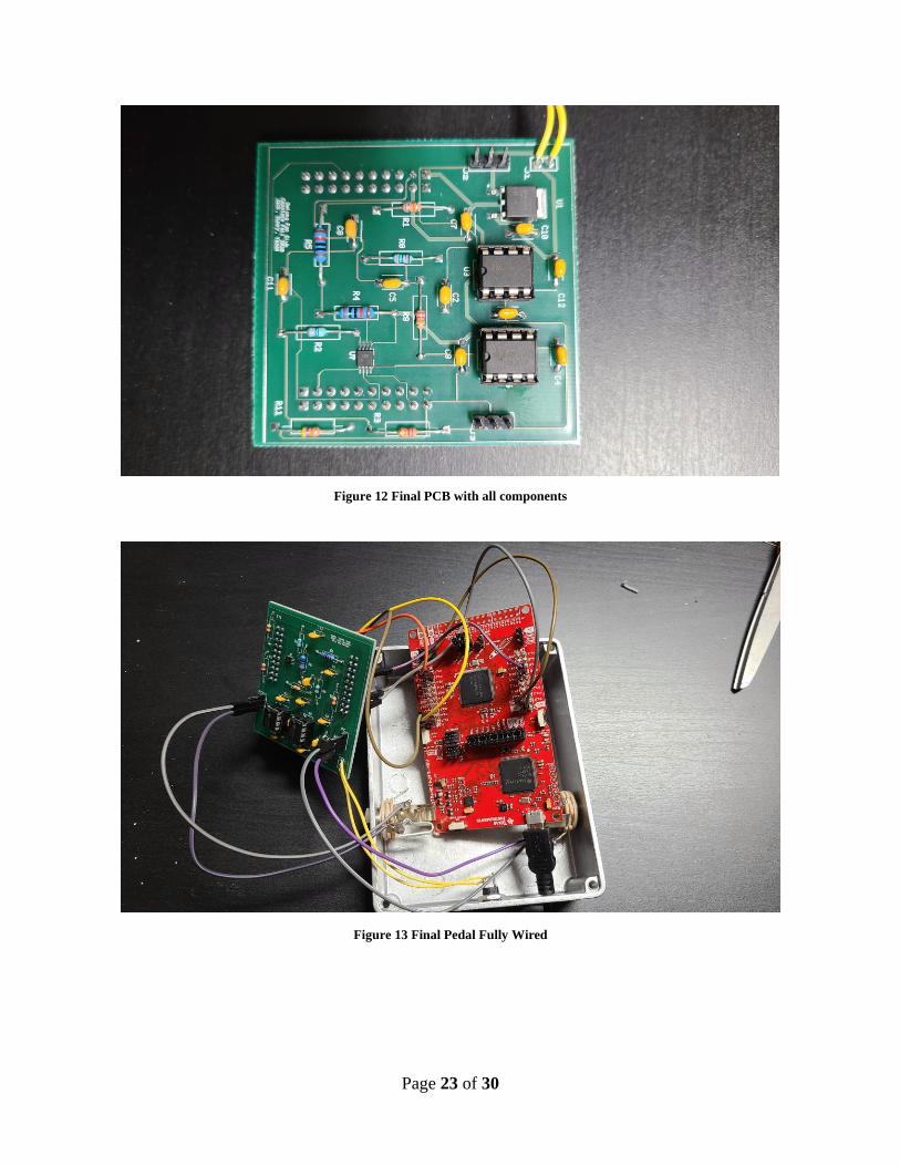
Figure 13 Final Pedal Fully Wired
Page 24 of 30
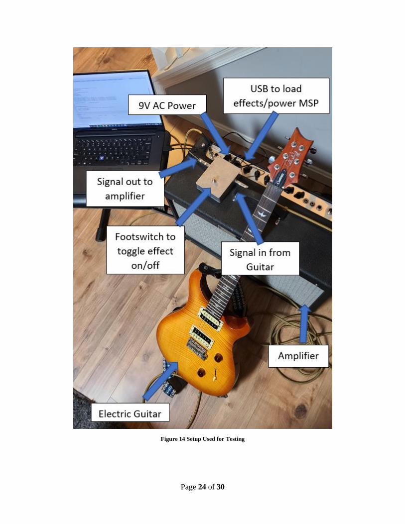
Figure 14 Setup Used for Testing
Page 25 of 30
Costs The total cost for this project was $120.96. A detailed spreadsheet of the costs can be found in
the appendix below but the cost breakdown is as follows:
● 2 PCB board sendouts: $66 ($33 per board)
● MSPEXP432P401R: $23.99
● Op amps: $1.68
● Voltage regulators: $2.88
● I/O Jacks: $4.92
● Resistors: $0.40
● Metal Enclosure: $13.96
● DAC8551: $6.09
● Pins: $ 0.36
When considering how manufacturing 10000 unit quantities effects the costs we see that the
price for each component bought in bulk is as follows:
● Op Amps: $0.19500 (originally $0.56)
● Voltage regulators: $0.52940 (originally $1.44)
● I/O Jacks: $1.52750 (originally $2.46)
● Resistors: $0.00653 (originally $0.1)
● Capacitors: $.045553 (originally $1.75)
● DAC8551: $3.06840 (originally $6.09)
● Pins: $0.06405 (originally $.18)
● Enclosure: $13.96
● MSP432P401R (chip only): $3.98766 (originally $7.72)
So given these prices, when creating these boards in bulk, the component costs go from $81.69
to $58.47 saving $23.22 per board made in bulk.
Automated equipment would be needed to assemble this board because of small parts such as the
DAC8551 and the MSP432P401R chip. Thus, the cost of manufacturing with this type of
equipment would need to be taken into account. Either contracting or hiring an established
company or renting/buying the equipment to do the board manufacturing will add more expense.
There are pros and cons to both of these options. For hiring an external company, machine
maintenance does not have to be taken into consideration and there will be experienced
personnel that will take care of the work. On the other hand, if the equipment was bought it
would be more expensive at the beginning than hiring a manufacturer but in the long run it may
be cheaper since a manufacturer has to continually be paid to do the work. Hiring another
established manufacturer is the better option since they have expertise and there will be less
stress about upgrading the equipment and hiring experienced workers. This however will be
costly and be thousands of dollars a year to maintain. Therefore, the sales price of the
manufactured guitar pedal will probably be around $100+ to pay for the components and
manufacturing but still make a profit.
Page 26 of 30
Future Work Had our team been given additional time to complete this project, we likely could have
implemented many of the guitar effects that we initially had planned for. The ability to be able
to load an effect onto the device at the end of the project was a major success for the project, and
provided a great platform for future effects to be created and uploaded to the device. The
creation of the effect “library” would have been extremely interesting to demonstrate, as the user
would be able to flip between multiple effects at the click of a button. Building on top of this,
the ability to make the effects library open-source would be an interesting idea, as guitar
players/coders from all over could contribute their code for different effects, providing end users
with many effects to choose from and load onto the device.
In hindsight the improvements that we would suggest to our initial plan are as follows: first and
foremost, the team should have planned to start the coding process in conjunction with the
hardware at the beginning of the project build period, rather than staggering the two processes
throughout the semester. This would have avoided the issue of running out of time after
finishing the DSP configuration on the MSP432 and not being able to code the effects we had
planned. Secondly, although our circuit design ended up working out and fitting inside the
enclosure, cleaner, more efficient wiring could be used in the future in order to tidy up the inside
of the pedal enclosure and thus make parts more modular and replaceable, should something
malfunction. The last improvement we would suggest is the addition of potentiometers that
could be programmed based on the effect. For this feature, we could map the ins and outs of the
potentiometer to pins on the MSP432 and use them to control other features of the signal, such as
equalization, addition of more or less gain, and duration of a delay effect.
Page 27 of 30
References
[1]C. Blasie, "Design of DSP Guitar Effects with FPGA Implementation", Scholarworks.rit.edu,
2020. [Online]. Available:
https://scholarworks.rit.edu/cgi/viewcontent.cgi?article=11514&context=theses.
[Accessed: 07- Sep- 2020].
[2]R. Nuzzaci, Mobile Guitar Effect Accessory & Application", Mil.ufl.edu, 2009. [Online].
Available: https://mil.ufl.edu/4924/docs/example_docs/Fujimaru_Nuzzaci_PDR.pdf.
[Accessed: 07- Sep- 2020].
[3]A. Lynham, "How to build guitar effects pedals", MusicRadar, 2020. [Online]. Available:
https://www.musicradar.com/tuition/guitars/how-to-build-guitar-effects-pedals-640441.
[Accessed: 07- Sep- 2020].
[4]Digikey.com. 2020. Digikey Electronics - Electronic Components Distributor.
[online] Available at: https://www.digikey.com [Accessed 10 December 2020].
[5] 3welec. 2020. [online] Available at: http://www.3welec.com [Accessed 10
December 2020].
[6]"Standardization Policies and Procedures of the National Electrical Manufacturers
Association", Nema.org, 2020. [Online]. Available:
https://www.nema.org/docs/default-source/standards-document-library/2020-edition-
of-spp74490ce679374b728d8d79ba3b077ca2.pdf?Status=Temp&sfvrsn=89d4df3d_13.
[Accessed: 08- Sep- 2020].
[7]"IPC Standards", Ipc.org, 2020. [Online]. Available:
https://www.ipc.org/CommitteePage.aspx. [Accessed: 08- Sep- 2020].
[8]NI Multisim Live. 2020. Multisim Live Online Circuit Simulator. [online] Available
at: https://www.multisim.com [Accessed 9 December 2020].
[9]Ni.com. 2020. Ultiboard. [online] Available at: https://www.ni.com/en-
us/shop/software/products/ultiboard.html [Accessed 9 December 2020].
[10]Ni.com. 2020. Virtualbench. [online] Available at: https://www.ni.com/en-
us/shop/electronic-test-instrumentation/virtualbench/what-is-virtualbench.html
[Accessed 10 December 2020].
[11]Ti.com. 2020. CCSTUDIO Code Composer Studio (CCS) Integrated Development
Environment (IDE) | TI.Com. [online] Available at:
https://www.ti.com/tool/CCSTUDIO [Accessed 9 December 2020].
[12] docking, m., signal, s., effect, v., process, r., materials, c., balsamita, C., Boogie,
M., application, c., process, c., reactions, c., substances, l. and materials, v., 2020.
Page 28 of 30
US8957297B2 - Programmable Musical Instrument Pedalboard - Google Patents.
[online] Patents.google.com. Available at:
https://patents.google.com/patent/US8957297?oq=programmable+multi+effects+pedal
[Accessed 11 December 2020].
[13] effects, c., materials, c., processes, e., signal, s., transmission, b., reactions, c., 1,
4., Values, N., reactions, e., biphenyls, p. and tapping, r., 2020. US20060278068A1 -
Guitar Pedal - Google Patents. [online] Patents.google.com. Available at:
https://patents.google.com/patent/US20060278068A1/en?q=%22guitar+pedal%22&oq
=%22guitar+pedal%22 [Accessed 11 December 2020].
[14] effects, c., signal, s., processes, e., effect, v. and transmission, b., 2020.
GB2456307A - Digital Control Of Analogue Music Effects Devices - Google Patents.
[online] Patents.google.com. Available at:
https://patents.google.com/patent/GB2456307A/en?q=%22guitar+pedal%22+effects&o
q=%22guitar+pedal%22+effects [Accessed 11 December 2020].
[15] Amazon.com. 2020. 9V Power Supply. [online] Available at:
https://www.amazon.com/Keyboard-DanElectro-DigiTech-Electronic-
LotFancy/dp/B07234PV7Q/ref=sr_1_2_sspa?crid=YEXRQB5CXGJC&dchild=1&key
words=9v+power+supply&qid=1607631340&sprefix=9v+power [Accessed 10
December 2020].
[16] 2020. 3.3V Voltage Regulator. [online] Available at:
https://www.digikey.com/en/products/detail/texas-instruments/LM1117DTX-3.3-
NOPB/3527434 [Accessed 10 December 2020].
[17] 2020. Ceramic Capacitors. [online] Available at:
https://www.digikey.com/en/products/filter/ceramic-
capacitors/60?s=N4IgTCBcDaIMYFMBOBDAtgSzgAjigDinBgC4D2SAziALoC%2B
QA [Accessed 10 December 2020].
[18] 2020. Through Hole Resistors. [online] Available at:
https://www.digikey.com/en/products/filter/through-hole-
resistors/53?s=N4IgTCBcDaIC4AsBOB7ArgcwQAgSgNgKbZKEDOAlmXCkmSALo
C%2BQA [Accessed 10 December 2020].
[19] 2020. NE5532 Operational Amplifier. [online] Available at:
https://www.digikey.com/en/products/detail/texas-instruments/NE5532P/277056
[Accessed 10 December 2020].
[20] 2020. Stereo Jack. [online] Available at:
https://www.digikey.com/en/products/detail/switchcraft-inc/12B/109541 [Accessed 10
December 2020].
Page 29 of 30
[21] 2020. MSP432P401R. [online] Available at:
https://www.digikey.com/en/products/detail/texas-instruments/MSP-
EXP432P401R/5170609 [Accessed 10 December 2020].
[22]"Signal Processing With a SimpleLinkTm Msp432TM Microcontroller and the
CMSIS-DSP Library", Ti.com, 2020. [Online]. Available:
https://www.ti.com/lit/an/slaa707a/slaa707a.pdf?ts=1600209470073&ref_url=https%25
3A%252F%252Fwww.google.com%252F. [Accessed: 08- Sep- 2020].
[22] 2020. DAC8551. [online] Available at:
https://www.digikey.com/en/products/detail/texas-
instruments/DAC8551IDGKR/5143029 [Accessed 10 December 2020].
[23] L. Glenn, "Differences between Overdrive, Distortion, and Fuzz ",
Web.pmtonline.co.uk, 2020. [Online]. Available:
https://www.pmtonline.co.uk/blog/2017/02/21/. [Accessed: 07- Sep- 2020].
[24]T. Schmitz, "Reshaping a Guitar Signal", ResearchGate, 2020. [Online]. Available:
https://www.researchgate.net/figure/Reshaping-a-guitar-signal-of-length-N-data-to-
have-N-data-N-1-instances-where-each_fig36_336945145. [Accessed: 07- Sep- 2020].
[25]D. Yeh, "DIGITAL IMPLEMENTATION OF MUSICAL DISTORTION
CIRCUITS BY ANALYSIS AND SIMULATION", Ccrma.stanford.edu, 2020.
[Online]. Available:
https://ccrma.stanford.edu/~dtyeh/papers/DavidYehThesissinglesided.pdf. [Accessed:
07- Sep- 2020].

Page 30 of 30
Appendix
Delong's Fan Club Items & Budget
Item Price Budget prepurchase Budget postpurchase
MSPEXP432P401R 23.99 250 226.01
OP AMP 1.12 226.01 224.89
3.3 V regulator 1.44 224.89 223.45
I/O jacks 4.92 223.45 218.53
36K Resistor 0.2 218.53 218.33
DAC8551 6.09 218.33 212.24
1X3 Pins 0.36 212.24 211.88
1x4 pins 0.68 211.88 211.2
Enclosure 13.96 211.2 197.24
36K Resistor 0.2 197.24 197.04
3.3 V regulator 1.44 197.04 195.6
OP AMP 0.56 195.6 195.04
PCB Board 33 195.04 162.04
PCB Board 33 162.04 129.04
Figure 15 Spreadsheet of purchases and budget
Github link to project code:
https://github.com/shresthayaman/CapstoneProject