Embed Size (px)
Citation preview

Project no.: IST-2005-034562
Project acronym: HIBISCUS
Project title: Hybrid integrated biophotonic sensors created by ultrafast laser systems Instrument: STREP Priority: [2] [Information Society Technologies]
Deliverable D3: Report on optical waveguide fabrication in glass substrates for biochips
Due date of deliverable: month 12 Actual submission date:
Start date of project: 01/09/2006 Duration: 36 months Organisation name of lead contractor for this deliverable: POLIMI Revision [draft]
Project co-funded by the European Commission within the Sixth Framework Programme (2002-2006) Dissemination Level
PU Public X PP Restricted to other programme participants (including the Commission Services) RE Restricted to a group specified by the consortium (including the Commission Services) CO Confidential, only for members of the consortium (including the Commission Services)
H I B I S C
U S
Project No. IST-2005-034562 (HIBISCUS) Deliverable D3
2
INDEX
1 – Introduction 3 2 – Femtosecond laser waveguide writing in different fused silica substrates 4 3 – Optical characterization of the fabricated waveguides 5 4 – Integration of optical waveguides with microfluidic channels
fabricated by femtosecond irradiation and chemical etching 8 5 – Integration of optical waveguides in commercial biochips 10
6 – Conclusions 15

Project No. IST-2005-034562 (HIBISCUS) Deliverable D3
3
1. Introduction
Deliverable D3 reports on the work performed within WP3 and addresses the key technological advance of this project, namely integration of optical waveguides, fabricated by femtosecond laser pulses, with microfluidic channels.
Figure 1 Optical waveguide writing by femtosecond lasers in biochips with microfluidic channels. Femtosecond waveguide manufacturing depends sensitively on the glass composition and the writing parameters. Microfluidic channel fabrication by standard techniques is performed on a limited number of glass types. In the first phase of the project we selected those glasses which are suitable for both microchannel and waveguide fabrication. In particular the investigation focused on fused silica which has the advantage of UV transparency enabling label-free molecule optical detection by targeting the polypeptide absorption. Waveguides have been optically characterized in terms of refractive index profiles and modal losses and the results have been sent to UTWENTE as the starting point for the simulations reported in Deliverable D4. After two suitable glass types have been selected, POLIMI and LIONIX prepared microfluidic channels on them. In particular, POLIMI used the innovative technique of femtosecond laser irradiation followed by chemical etching (subject of WP4) and LIONIX used conventional microfabrication technologies for commercial lab-on-chips (LOCs). Waveguides have been inscribed in the substrates with microfluidic channels. Simple geometries have been implemented such as straight waveguides crossing the channels perpendicularly in order to allow detection of biomolecules by absorption/fluorescence. Excitation of fluorescent molecules filling the microfluidic channels has been demonstrated.

Project No. IST-2005-034562 (HIBISCUS) Deliverable D3
4
2. Femtosecond laser waveguide writing in different fused silica substrates
The set-up for manufacturing optical waveguides inside glass samples by femtosecond laser pulses is very simple and is schematized in Fig. 2. A femtosecond laser is focused by a microscope objective inside the sample, which is in turn moved by motorized translation stages.
Figure 2 Femtosecond laser writing set-up.
Thanks to the nonlinear absorption mechanism very localized modifications can be induced in the volume. The unique features of this fabrication technique are: (i) it is a direct technique, since waveguides are fabricated in a single step, by simple translation of the sample; (ii) it is a three-dimensional technique, since waveguides can be placed at any depth from the sample surface between a few tens and several hundreds of microns. The initial experiments were performed with an amplified Ti:sapphire laser (800-nm wavelength, 150-fs pulsewidth) at 1 kHz repetition rate. In this case an astigmatic beam shaping technique (patented by POLIMI) is necessary in order to achieve a symmetric waveguide cross section1. The shaping is implemented by a cylindrical telescope, as shown in Fig. 2. Initially POLIMI fabricated straight optical waveguides on some commercial fused silica substrates. In particular, fused silica samples from SCHOTT (Lithosil), CORNING (HPFS) and FOCTEK have been tested. These choices are motivated by the fact that the former two are routinely used by LIONIX for microchip fabrication, while on the latter one, POLIMI has developed a procedure for microchannel fabrication by means of femtosecond irradiation followed by selective chemical etching2 (further developed in WP4). Fig. 3 shows some images of a typical waveguide, fabricated with a 20× objective (0.3 NA), 4 µJ pulse energy and a translation speed of 10 µm/s. The top-view clearly 1 R. Osellame, S. Taccheo, M. Marangoni, R. Ramponi, P. Laporta, D. Polli, S. De Silvestri, G. Cerullo, J. Opt. Soc. Am. B 20, 1559 (2003). 2 V. Maselli, R. Osellame, G. Cerullo, R. Ramponi, P. Laporta, L. Magagnin and P. L. Cavallotti, Appl. Phys. Lett. 88, 191107 (2006).
µscope objective
Femtosecond laser
Mirror
Translation stage
Glass substrate
Cylindrical telescope

Project No. IST-2005-034562 (HIBISCUS) Deliverable D3
5
evidences the waveguide uniformity, which is a key-point for achieving low propagation losses. The end-view shows that the waveguide has a perfectly circular cross-section with a diameter of about 10 µm. Such symmetric cross-section can be obtained thanks to the use of the astigmatic beam shaping technique. This is a very important feature if a fundamental circularly-shaped guided mode in the visible is required; this would in fact increase significantly the mode-matching, and thus the coupling efficiency, with optical fibers. It is worth noting that the material modification is strictly limited to the focal volume of the writing beam; this is quite important for optical sensing in LOCs where the position of the waveguides with respect to the microfluidic channels is very important, thus a fine control of the position and shape of the modified region is required.
Figure 3 Scheme and microscope images (top and end view) of a femtosecond laser written waveguide.
In addition, the astigmatic beam shaping technique has been employed also for the fabrication of waveguides with slightly elliptically-shaped cross-sections. This would help removing the degeneracy between quasi-TE and quasi-TM modes thus allowing single polarization operation which would be important for interferometric devices. Such waveguides are now under testing at UTWENTE and their use in the final devices will be evaluated.
3. Optical characterization of the fabricated waveguides The optical characteristics of the waveguides were investigated by coupling light at different wavelengths, from the red (632 nm) to the green (543 nm) to the UV (375 nm). Different results have been obtained for the different fused silica suppliers. The best results in terms of propagation losses, single mode operation and symmetry of the fabricated waveguides have been found on the SCHOTT sample, to whom all the below characterization measurements refer. As a consequence such substrate has been chosen as the one to be used for the microfluidic chip fabrication at LIONIX. However, results on the other substrates were only slightly worse, thus they have not been discarded but they
X
Y
100 µm
Experimental
10 µm
Experimental
Z
Y

Project No. IST-2005-034562 (HIBISCUS) Deliverable D3
6
are kept as a second choice, which could be re-evaluated in the future on the basis of commercial or economical reasons. The waveguides were found to be single-mode at all visible-UV wavelengths (see near-field mode profiles in Fig. 4). The maximum refractive index changes were retrieved using a mode solver software assuming a Gaussian refractive index profile, and were found to range from 3×10⁻⁴ to 7×10⁻⁴; such values are in good agreement with a direct measurement of the refractive index profile by a commercial Refractive Near-Field refractometer (RNF by Rinck Elektronik), giving ∆n=8.5×10⁻⁴ (see Fig.5).
Figure 4 Near-fields of the guides mode of a fs laser written waveguide in the UV-visible range. The
estimated maximum refractive index change is reported below each panel.
Figure 5 Refractive index profile of a fs-laser-written waveguide measured by a RNF refractometer.
The above results evidences a very peculiar behavior of femtosecond laser written waveguides. It is indeed very uncommon that a waveguide is single mode in the whole UV-visible range, keeping in addition almost the same mode dimensions. As presented above, this is made possible only thanks to an increase of the refractive index change with wavelength, which is the opposite of what is usually observed in waveguides fabricated with standard techniques. A first prediction of such peculiar behavior is reported in Fig. 6 showing the results of a theoretical ab initio calculation3. The dot-dashed line represent the modified refractive index of fused silica, with respect to the substrate one (solid line), after femtosecond laser irradiation. Notwithstanding the very different absolute values of the refractive indexes with respect to the experimental ones, a clear decrease of the refractive index change in the UV region is predicted. Our results 3 S. Sen and J.E. Dickinson, Phys. Rev. B 68, 214204 (2003)
5 µm
λ = 633 nmλ = 543 nm
(c)(a) (b)
λ = 375 nm
∆n = 3x10⁻⁴ ∆n = 6.3x10⁻⁴ ∆n = 7x10⁻⁴
1.4560
1.4565
1.4570
1.4560
1.4565
1.4570
0 5 10 15 20 25 30 350
5
10
15
20
25
30
35
x(µm)
y (µ
m)
refractive index wg 3
n
n

Project No. IST-2005-034562 (HIBISCUS) Deliverable D3
7
are the first experimental evidence of such behavior and further investigation will be performed in order to fully understand the physical mechanism.
Figure 6 Calculated wavelength dependence of the refractive indexes of the original fused silica (solid
line) and of the laser modified region (dashed-dot line). Apart from the wavelength dependence of the refractive index change, it is worth noting that the experimental value achieved is rather low (below 10-3). This, on one side allows single mode operation even for 10 µm diameter waveguides, but on the other side is a limitation for curved waveguides, due to significant bending losses for small curvature radii (see Deliverable D4). This could indeed be a problem for the project goals since splitters and interferometers need to be produced in order to implement a sophisticated on chip optical sensing. To overcome this limitation two actions will be taken: on one hand, a clever design of the microfluidic and optical devices will be performed in order to increase as much as possible the curvature radii of the optical waveguides; on the other hand, different femtosecond laser sources will be employed, i.e. the new laser sources developed in WP1, that due to a higher repetition rate should increase the refractive index change in fused silica as happened in other glass samples.
Figure 7 Propagation losses measured with the cut-back technique. Propagation losses at 543 nm were measured using the cut-back technique. The 1.8 cm long waveguides set was cut back to 1.1 and 0.6 cm, and insertion loss measurements
Sen et al., Phys. Rev. B, 2003
Theoretical

Project No. IST-2005-034562 (HIBISCUS) Deliverable D3
8
with microscope objectives coupling were repeatedly performed taking care to keep the same coupling conditions for each sample length. The results provided propagation losses of 0.9 dB/cm (see Fig. 7). This value is very promising as compared to those obtained at similar wavelengths on other kinds of waveguides that can be integrated on LOCs and fabricated with SU-8 polymer4 (2.5 dB/cm) and with SiON technology5 (1 dB/cm) (see Table 1). Since the main cause of propagation losses in femtosecond laser written waveguides is the scattering induced by microbendings due to mechanical vibrations in the writing process, even better values of propagation losses can be foreseen with improved air-bearing translation stages, now available at POLIMI.
Table 1 Propagation losses in the green measured in waveguides fabricated with different techniques than femtosecond laser writing.
In summary, the femtosecond laser written waveguides in fused silica display low losses and single-mode guidance in the visible range. Such results are very promising for the integration of straight waveguides into microfluidic LOCs.
4. Integration of optical waveguides with microfluidic channels fabricated by femtosecond irradiation and chemical etching
The key goal of the HIBISCUS project is the integration of optical waveguides with microfluidic channels in order to implement on-chip optical sensing. Given the very high quality of the previously reported optical waveguides, POLIMI started to investigate such integration by fabricating on the same chip both the optical waveguides and the microfluidic channel by femtosecond lasers. The femtosecond laser fabrication of microfluidic channels is the main objective of WP4 and a complete description is beyond the scope of this report, which is focused on the fabrication of optical waveguides. However, femtosecond laser irradiation followed by chemical etching in an HF water solution provides selective etching along the irradiated track and results in the formation of very high-aspect-ratio, directly-buried, void channels. Figure 8 reports the main features of such channels: (a) etching from just one side causes a conical shape; (b) etching from both sides of the samples provides a through channel of a few millimeters length with a 50 µm narrow passage in the middle; (c) with a smaller distance of the two etching sides an almost uniform through channel with 100 µm diameter and 2 mm length is obtained; (d) the cross-section of the channel is circular due to the employment of the
4 K. B. Mogensen, J. El-Ali, A. Wolff, and J. P. Kutter, Appl. Opt. 42, 4072 (2003). 5 K. B. Mogensen, P. Friis, J. Hubner, N. J. Petersen, A. M. Jorgensen, P. Telleman, and J. P. Kutter, Opt. Lett. 26, 716 (2001).
Opt. Lett. 26, 716 (2001) 1 dB/cm SiON
Appl. Opt. 42, 4072 (2003) 2.5 dB/cm Polymer SU-8
Reference Losses in the green
Waveguide Material

Project No. IST-2005-034562 (HIBISCUS) Deliverable D3
9
astigmatic beam shaping technique and three-dimensional packaging of the microfluidic channels is easily obtained.
Figure 8 Microscope images of some microfluidic channels fabricated by femtosecond laser irradiation followed by chemical etching.
In order to demonstrate the integration capabilities of femtosecond laser fabrication technology, three waveguides spaced by 200 µm have been inscribed crossing the central region of the 2.2 mm microchannel [Fig. 8(c)], according to the scheme depicted in Fig. 9(a). The waveguide writing extends until inside the microfluidic channel without any evident damage of the microchannel walls.
Figure 9 (a) Schematic of the waveguides crossing the microfluidic channel; (b) microscope image of the microfluidic channel with the fluorescence excited by the optical waveguides; (c) intensity profile
acquired in the middle of the microchannel (y axis in previous panel) across one of the fluorescent filaments.
The microfluidic channel is filled by immersion in a solution of rhodamine 6G and ethylene glycol. When coupling the 543 nm light in one waveguide by means of an optical fiber, yellow fluorescence is visible from the microfluidic channel [Fig. 9(b)] through a long-pass filter (OG550 from Schott), rejecting the excitation light. No stray
µfluidicchanneloptical
waveguidesin-couplingfiber
opticalwaveguides
µfluidicchannel
100 mµ
(a)
(b)
(c)
y axis [µm]
Inte
nsity
[dB]
0 120 20040 80 16010
20
30
20 dB
y

Project No. IST-2005-034562 (HIBISCUS) Deliverable D3
10
light coming from waveguide scattering reaches the microfluidic channel, thus the excitation is very selective in space. Figure 9(c) shows the intensity profile acquired by a CCD camera across the fluorescent filament in the middle of the microchannel. The full width at half maximum of the fluorescent signal is equal to the waveguide mode diameter of 11 µm, in agreement with a Rayleigh range exceeding 200 µm. On the other hand, the very good signal-to-noise ratio of the fluorescence (about 20 dB) is a demonstration of the high waveguide quality. Coupling each of the three waveguides provides a fluorescent signal at three different points of the microfluidic channel [see the three panels in Fig. 9(b)]. This demonstrates the possibility of parallel multiple sensing at different positions in the microchannel, that could be achieved employing an external fiber splitter or preferably by integrating a femtosecond laser written waveguide splitter on the same chip. In summary, we demonstrated the integration on a fused silica substrate of microfluidic channels and optical waveguides, both fabricated by femtosecond laser pulses. This result has a twofold implication: on one hand, it introduces a powerful method for the direct integration of optical waveguide sensing in LOCs; on the other hand, it indicates the possibility of using a single production tool for the fabrication of both the microfluidic channels and the optical waveguides required for biophotonic sensors. However, it should be noted that the microfluidic channels fabricated by femtosecond laser irradiation and chemical etching are at present too short for practical applications. Therefore, to reach the goals of the project it is important to demonstrate waveguide integration in LOCs fabricated with conventional techniques.
5. Integration of optical waveguides in commercial biochips The next challenge was the integration of the optical waveguides in commercial LOC devices, provided by LIONIX. Figure 10 presents a layout of the microfluidic chip designed and manufactured by LIONIX for microchip capillary electrophoresis (blue lines correspond to microfluidic channels and small blue circles to reservoirs). The basic idea would be to integrate the optical sensing by inscribing some waveguides at the end of the separation channel in order to detect separately the components of the sample by laser induced fluorescence (LIF).
Figure 10 Schematic layout of a commercial lab-on-chip for capillary electrophoresis. The femtosecond laser written waveguides are depicted in red.
fs-writing laser
In-coupling
Out-coupling

Project No. IST-2005-034562 (HIBISCUS) Deliverable D3
11
The microfluidic channels this time are smaller than those presented in the previous section, with a rectangular cross-section measuring 50×12 µm2. The alignment of the optical waveguide with respect to the microfluidic channel is thus quite challenging, in particular in the depth direction where the microfluidic channel dimension is smaller. The femtosecond laser direction is reported in Fig. 10. A specific alignment procedure was developed, which exploits the back-reflection of a He-Ne laser, superimposed to the femtosecond one, from the air-glass interface at the microfluidic channel walls. This allows a control of the waveguide position with respect to the microfluidic channel with a precision within 2 µm. Several waveguides have been fabricated, either tangent to the microfluidic channel, for evanescent sensing, or crossing it for direct excitation. Figure 11 shows some microscope images of the optical waveguides end-view together with the microfluidic channel. From left to right, the position control can be appreciated with a waveguide slightly above the microfluidic channel, one slightly below and three perfectly centred (in the third image the microfluidic channel is out of focus, otherwise it would have been impossible to see the centred optical waveguides).
Figure 11 Microscope end-view images of some optical waveguides, orthogonal lto and either tangent
or crossing the microfluidic channel. Damaging of the channel walls when the writing laser crosses them was observed. Figure 12 shows a top-view of a microfluidic channel with 5 optical waveguides crossing it. Due to the low refractive index change the waveguides are not visible, therefore their position is highlighted by an orange line. The first four waveguides (from left to right) are fabricated with decreasing pulse energy (from 5 to 2 µJ), but they all cause damaging of the channel wall at the crossing. This damaging is very detrimental to our application since it both spoils the flow in the channel and introduces scattering in the light transmitted from the waveguide to the channel. This problem was solved by interrupting the writing beam a few microns before the channel and restoring it just after. This was possible by synchronizing a beam shutter with the driver of the translation stages. Due to the low numerical aperture of the waveguides, the Rayleigh range of the light coming out of them exceeds 100 µm, therefore it remains quite confined across the channel even if the waveguide stops a few micron before. On the other hand, since the waveguide writing
fs-writing laserµ-fluidic channel
Waveguides

Project No. IST-2005-034562 (HIBISCUS) Deliverable D3
12
is performed very close to the bonding surface between the two glass slabs that seal the microfluidic channels, it is important to note that no detectable damage was induced in the bonding region, demonstrating that the two glasses behave as a bulk piece.
Figure 12 Top-view of a microfluidic channel. Optical waveguides crossing the channel are not visible due to the low refractive index change and are therefore indicated by artificial orange lines.
The waveguides displayed very good optical properties, with excess loss of 1 dB when crossing a microfluidic empty channel. Figure 13 shows some near-field images of the coupled waveguides. The coupling was intentionally not optimized in order to have enough light out of the waveguide to also visualize the microfluidic channel (dark horizontal line). The three panels in Fig.13 correspond to the three situations reported in the microscope images of Fig.11 and demonstrate that the light is well guided both for waveguides slightly above/below the microfluidic channel and for waveguides exactly centred.
Figure 13 Near –field of the waveguide output in different configurations with respect to the microfluidic channel.
By using an optical waveguide to excite the content of a microfluidic channel filled with a fluorescing dye (Rhodamine 6G), it was possible to observe fluorescence from a very small volume of sample (see Fig. 14), thus demonstrating the capability of waveguides to perform local excitation with high spatial selectivity.
fs-writing laser
µ-fluidic channel
Waveguide slightly above
Waveguide slightly below Waveguide centered
Microfluidic channel

Project No. IST-2005-034562 (HIBISCUS) Deliverable D3
13
Figure 14 Microscope image of the fluorescence in the microfluidic channel filled with a fluorescent dye excited by a femtosecond laser written optical waveguide .
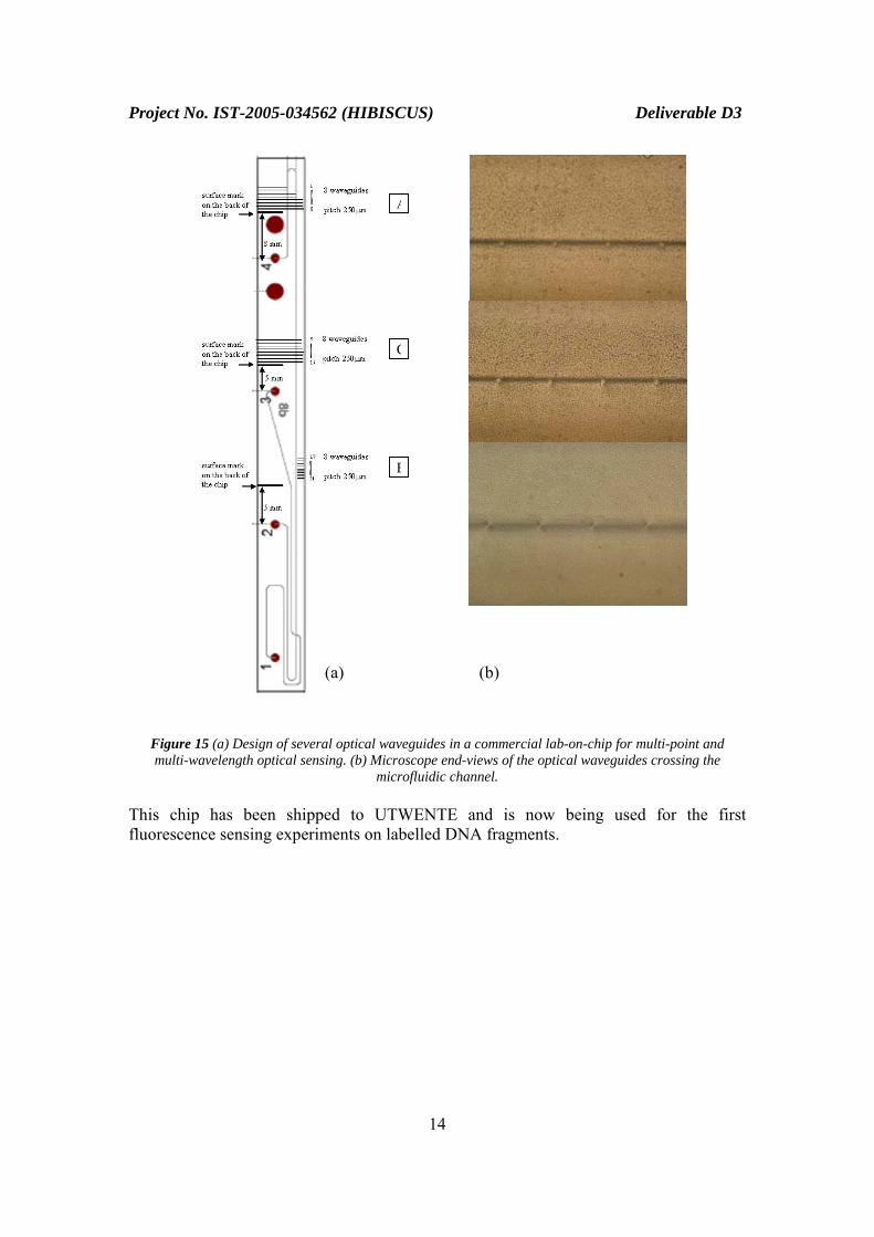
The importance of this result with respect to that presented in Fig.9 is that the waveguide is integrated in a commercial lab-on-chip where capillary electrophoresis has been already demonstrated, thus we are very close to the possibility of employing these waveguides for a real on chip fluorescence detection in bioassay applications. In order to exploit this result, UTWENTE provided a design of several waveguides on a LIONIX commercial biochip (see Fig.15a). This design aimed at demonstrating multi-point and multi-wavelength on-chip sensing, keeping also into account the layout of the cartridge that interfaces the chip with the high voltage driver for the electro-osmotic flow. The three groups of waveguides have been fabricated by POLIMI according to the design of UTWENTE. The waveguides have been analyzed under a microscope in order to verify their quality and alignment with the microfluidic channel. As shown in Fig.15b, all the waveguides have a fairly round cross-section and are very well aligned with the microfluidic channel. Light was coupled into the waveguides, thus verifying the good optical quality of all of them. The spacing between the waveguides in each group was selected as 250 µm in order to use standard fiber ribbons to simultaneously couple several waveguides. In order to overcome the difficulty of “seeing” the optical waveguides due to the low refractive index change, surface marks for aligning purposes have been produced on the back of the chip in correspondence of each waveguide group by the same femtosecond laser used to fabricate the waveguides.
Optical waveguide
Blow-up
50 µm
10 µm
Project No. IST-2005-034562 (HIBISCUS) Deliverable D3
14
Figure 15 (a) Design of several optical waveguides in a commercial lab-on-chip for multi-point and multi-wavelength optical sensing. (b) Microscope end-views of the optical waveguides crossing the
microfluidic channel. This chip has been shipped to UTWENTE and is now being used for the first fluorescence sensing experiments on labelled DNA fragments.
A
B
C
(a) (b)

Project No. IST-2005-034562 (HIBISCUS) Deliverable D3
15
6. Conclusions
In this deliverable we have demonstrated:
The main problems to overcome now are:
To overcome these obstacles we propose to:
• Optical waveguides fabricated in fused silica by femtosecond laser pulses with:high uniformity; round cross-section; very low propagation losses; singlemode operation in the whole visible range.
• Capability of integrating such waveguides with microfluidic channels
fabricated by laser sensitization and chemical etching.
• Fabrication of optical waveguides in commercial biochips and demonstration of
selective excitation of a dye in the microfluidic channel. • Manufacturing of several waveguides in a commercial biochips for multi-point
and multi-wavelength fluorescence sensing.
• Only straight waveguides have been manufactured until now. In order to producemore complex devices, e.g. splitters and interferometers, a specific software for2D or 3D translations with uniform velocity is needed to drive the translationstages.
• The refractive index change achieved in the waveguides (∆n~7×10⁻⁴) is too low
to allow small radii in curved waveguides. In order to keep the chip dimensionssmall, higher refractive index change is required.
• Develop a software dedicated to the air-bearing three-axis translation stagesowned by POLIMI in order to write arbitrarily curved waveguides in 3D.
• Use a higher repetition rate femtosecond laser (600 kHz instead of 1 kHz) and/or
use the second harmonic of such laser to increase the energy absorbed by thematerial and thus increase the material modification. This should lead to a higherrefractive index change.