Embed Size (px)
Citation preview
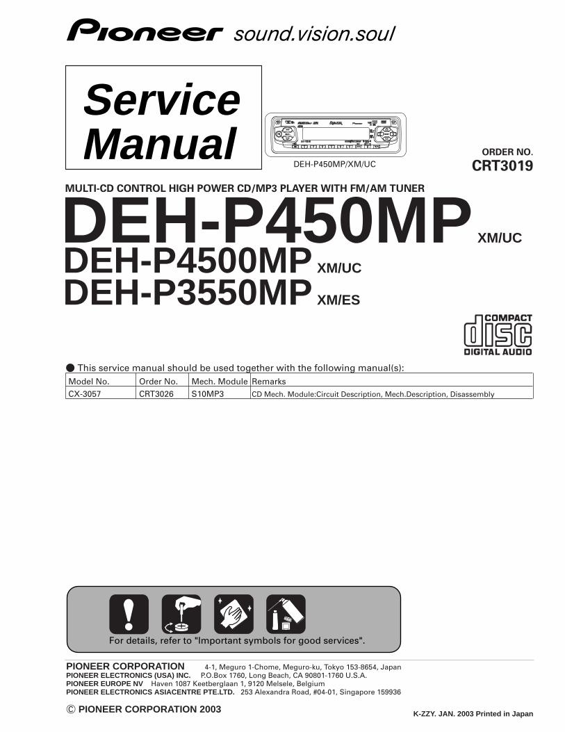
PIONEER CORPORATION 4-1, Meguro 1-Chome, Meguro-ku, Tokyo 153-8654, Japan PIONEER ELECTRONICS (USA) INC. P.O.Box 1760, Long Beach, CA 90801-1760 U.S.A.PIONEER EUROPE NV Haven 1087 Keetberglaan 1, 9120 Melsele, Belgium PIONEER ELECTRONICS ASIACENTRE PTE.LTD. 253 Alexandra Road, #04-01, Singapore 159936
C PIONEER CORPORATION 2003 K-ZZY. JAN. 2003 Printed in Japan
ORDER NO.
CRT3019
MULTI-CD CONTROL HIGH POWER CD/MP3 PLAYER WITH FM/AM TUNER
DEH-P450MPXM/UC
ServiceManual
DEH-P450MP/XM/UC
- This service manual should be used together with the following manual(s):Model No. Order No. Mech. Module Remarks
CX-3057 CRT3026 S10MP3 CD Mech. Module:Circuit Description, Mech.Description, Disassembly
DEH-P4500MP XM/UC
For details, refer to "Important symbols for good services".
DEH-P3550MP XM/ES
2
1 2 3 4
1 2 3 4
F
E
D
C
B
A
DEH-P450MP/XM/UC
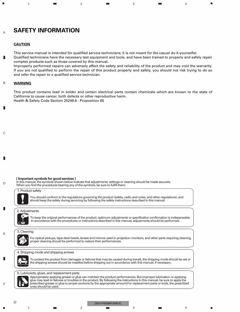
SAFETY INFORMATION
[ Important symbols for good services ]In this manual, the symbols shown-below indicate that adjustments, settings or cleaning should be made securely.When you find the procedures bearing any of the symbols, be sure to fulfill them:
2. Adjustments
To keep the original performances of the product, optimum adjustments or specification confirmation is indispensable. In accordance with the procedures or instructions described in this manual, adjustments should be performed.
3. Cleaning
For optical pickups, tape-deck heads, lenses and mirrors used in projection monitors, and other parts requiring cleaning,proper cleaning should be performed to restore their performances.
5. Lubricants, glues, and replacement partsAppropriately applying grease or glue can maintain the product performances. But improper lubrication or applying glue may lead to failures or troubles in the product. By following the instructions in this manual, be sure to apply theprescribed grease or glue to proper portions by the appropriate amount.For replacement parts or tools, the prescribed ones should be used.
4. Shipping mode and shipping screws
To protect the product from damages or failures that may be caused during transit, the shipping mode should be set orthe shipping screws should be installed before shipping out in accordance with this manual, if necessary.
1. Product safety
You should conform to the regulations governing the product (safety, radio and noise, and other regulations), and should keep the safety during servicing by following the safety instructions described in this manual.
CAUTION
This service manual is intended for qualified service technicians; it is not meant for the casual do-it-yourselfer.Qualified technicians have the necessary test equipment and tools, and have been trained to properly and safely repaircomplex products such as those covered by this manual.Improperly performed repairs can adversely affect the safety and reliability of the product and may void the warranty.If you are not qualified to perform the repair of this product properly and safely, you should not risk trying to do soand refer the repair to a qualified service technician.
WARNING
This product contains lead in solder and certain electrical parts contain chemicals which are known to the state ofCalifornia to cause cancer, birth defects or other reproductive harm. Health & Safety Code Section 25249.6 - Proposition 65
3
5 6 7 8
F
E
D
C
B
A
5 6 7 8DEH-P450MP/XM/UC
- CD Player Service Precautions
1. Before disassembling the unit, be sure to turn off the
power. Unplugging and plugging the connectors dur-
ing power-on mode may damage the ICs inside the
unit.
2. To protect the pickup unit from electrostatic dis-
charge during serviving, take an appropriate treat-
ment(shorting-solder) by referring to "the DISAS-
SEMBLY" on page 55.
3. After replacing the pickup unit, be sure to check the
grating.(See p.52.)
CONTENTS
SAFETY INFORMATION ............................................................................................................................................2
1. SPECIFICATIONS .......................................................................................................................................................4
2. EXPLODED VIEWS AND PARTS LIST.......................................................................................................................6
2.1 PACKING...............................................................................................................................................................6
2.2 EXTERIOR (DEH-P450MP, P4500MP)..................................................................................................................8
2.3 EXTERIOR (DEH-P3550MP) ...............................................................................................................................12
2.4 CD MECHANISM MODULE ...............................................................................................................................14
3. BLOCK DIAGRAM AND SCHEMATIC DIAGRAM...................................................................................................16
3.1 BLOCK DIAGRAM ..............................................................................................................................................16
3.2 OVERALL CONNECTION DIAGRAM(GUIDE PAGE) ........................................................................................18
3.3 KEYBOARD UNIT ...............................................................................................................................................24
3.4 CD MECHANISM MODULE ...............................................................................................................................26
4. PCB CONNECTION DIAGRAM................................................................................................................................36
4.1 TUNER AMP UNIT .............................................................................................................................................36
4.2 PANEL UNIT .......................................................................................................................................................40
4.3 KEYBOARD UNIT ...............................................................................................................................................41
4.4 CD MECHANISM MODULE ...............................................................................................................................42
5. ELECTRICAL PARTS LIST ........................................................................................................................................44
6. ADJUSTMENT .........................................................................................................................................................49
6.1 JIG CONNECTION DIAGRAM ...........................................................................................................................49
6.2 CD ADJUSTMENT .............................................................................................................................................50
6.3 CHECKING THE GRATING AFTER CHANGING THE PICKUP UNIT................................................................52
6.4 ERROR MODE ....................................................................................................................................................54
7. GENERAL INFORMATION .......................................................................................................................................55
7.1 DIAGNOSIS ........................................................................................................................................................55
7.1.1 DISASSEMBLY ..............................................................................................................................................55
7.1.2 CONNECTOR FUNCTION DESCRIPTION....................................................................................................57
7.2 PARTS .................................................................................................................................................................59
7.2.1 IC ....................................................................................................................................................................59
7.2.2 DISPLAY.........................................................................................................................................................68
7.3 OPERATIONAL FLOW CHART...........................................................................................................................70
7.4 CLEANING..........................................................................................................................................................71
8. OPERATIONS ...........................................................................................................................................................72

1. SPECIFICATIONS
4
1 2 3 4
1 2 3 4
F
E
D
C
B
A
DEH-P450MP/XM/UC
- DEH-P450MP/XM/UC, P4500MP/XM/UC

5
5 6 7 8
F
E
D
C
B
A
5 6 7 8DEH-P450MP/XM/UC
- DEH-P3550MP/XM/ES
6
1 2 3 4
1 2 3 4
F
E
D
C
B
A
DEH-P450MP/XM/UC
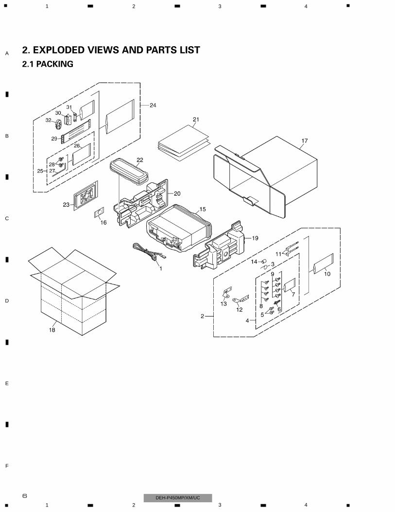
2. EXPLODED VIEWS AND PARTS LIST
2.1 PACKING
7
5 6 7 8
F
E
D
C
B
A
5 6 7 8DEH-P450MP/XM/UC
- PACKING SECTION PARTS LIST
NOTE:
- Parts marked by “*” are generally unavailable because they are not in our Master Spare Parts List.
- Screws adjacent to ∇ mark on the product are used for disassembly.
- For the applying amount of lubricants or glue, follow the instructions in this manual.
(In the case of no amount instructions, apply as you think it appropriate.)
- Owner's Manual, Installation ManualModel Part No. LanguageDEH-P450MP/XM/UC CRD3676 English, French, Spanish
CRD3677DEH-P4500MP/XM/UC CRD3678 English, French, Spanish
CRD3679DEH-P3550MP/XM/ES CRD3680 English, Spanish, Portuguese(B)
CRD3681 Arabic, ChineseCRD3682 English, Spanish, Portuguese(B), Arabic, Chinese
Part No.Mark No. Symbol and Description DEH-P450MP/XM/UC DEH-P4500MP/XM/UC DEH-P3550MP/XM/ES
1 Cord Assy CDE7060 CDE7060 CDE70602 Accessory Assy CEA3376 CEA3376 CEA34393 Spring CBH1650 CBH1650 CBH16504 Screw Assy CEA3445 CEA3445 CEA34375 Fixing Screw BPZ20P060FZK BPZ20P060FZK Not used
6 Screw CBA1002 CBA1002 CBA1002* 7 Polyethylene Bag CEG-127 CEG-127 CEG-127
8 Screw CRZ50P090FTC CRZ50P090FTC CRZ50P090FTC9 Screw TRZ50P080FTC TRZ50P080FTC TRZ50P080FTC
* 10 Polyethylene Bag CEG-158 CEG-158 CEG-158
11 Handle CNC5395 CNC5395 CNC539512 Holder CND1249 CND1249 Not used13 Holder CND1250 CND1250 Not used14 Bush CNV3930 CNV3930 CNV393015 Polyethylene Bag CEG1173 CEG1173 CEG-162
* 16 Battery CEX1030 CEX1065 Not used17 Carton CHG4952 CHG4953 CHG495418 Contain Box CHL4952 CHL4953 CHL495419 Protector CHP2663 CHP2663 CHP266320 Protector CHP2664 CHP2664 CHP2664
21-1 Owner’s Manual CRD3676 CRD3678 CRD368021-2 Owner’s Manual Not used Not used CRD368121-3 Installation Manual CRD3677 CRD3679 CRD3682
* 21-4 Warranty Card CRY1070 Not used Not used* 21-5 Card Not used ARY1048 Not used
* 21-6 Caution Card Not used CRP1294 Not used22 Case Assy CXB3520 CXB3520 CXB352023 Remote Control Unit Not used CXC1265 Not used24 Remote Control Assy CXB9202 Not used Not used25 Screw Assy CZE3169 Not used Not used
* 26 Polyethylene Bag CEG-127 Not used Not used* 27 Hexagonal Wrench CZE3176 Not used Not used* 28 Screw RMZ30H060FBK Not used Not used
29 Belt CZN7661 Not used Not used30 Holder Assy CZX3172 Not used Not used
31 Holder Assy CZX3173 Not used Not used32 Remote Control Assy CZX3257 Not used Not used
8
1 2 3 4
1 2 3 4
F
E
D
C
B
A
DEH-P450MP/XM/UC
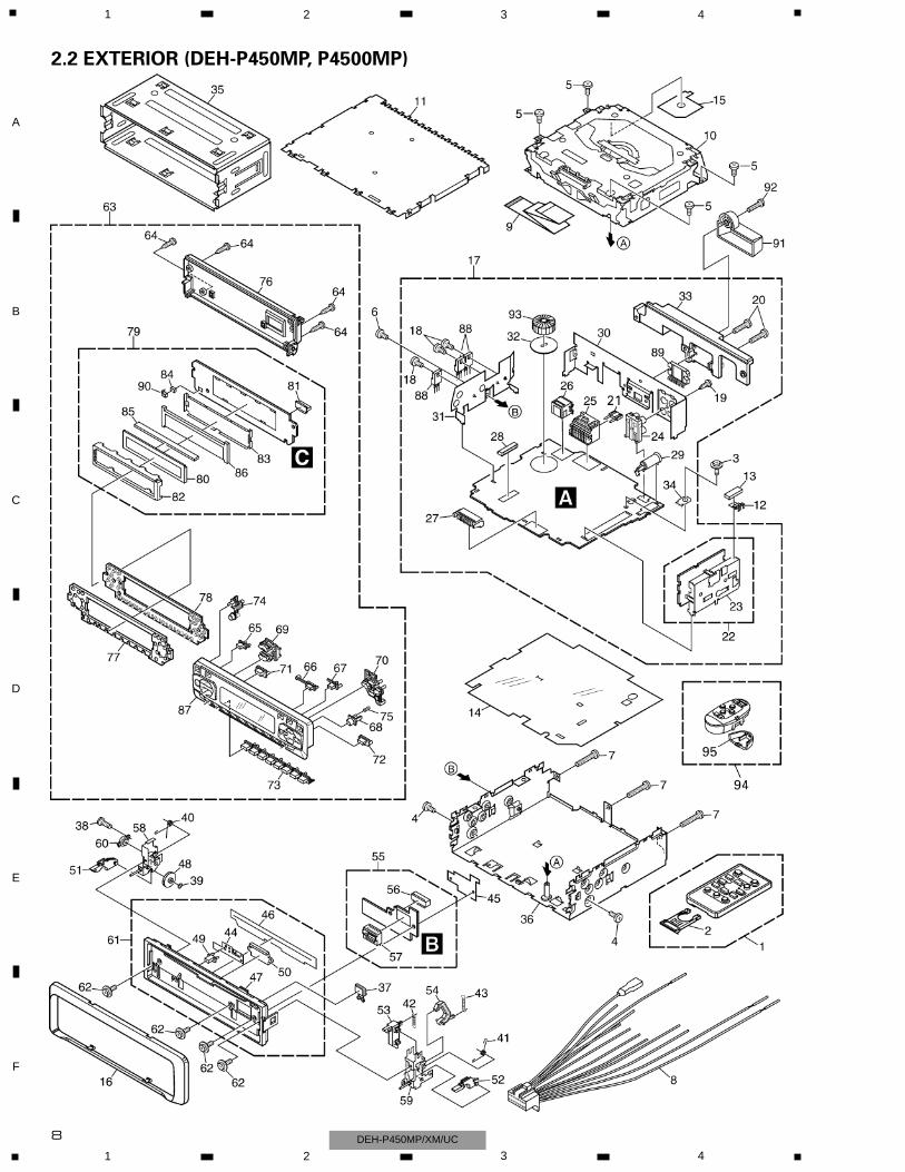
2.2 EXTERIOR (DEH-P450MP, P4500MP)
9
5 6 7 8
F
E
D
C
B
A
5 6 7 8DEH-P450MP/XM/UC
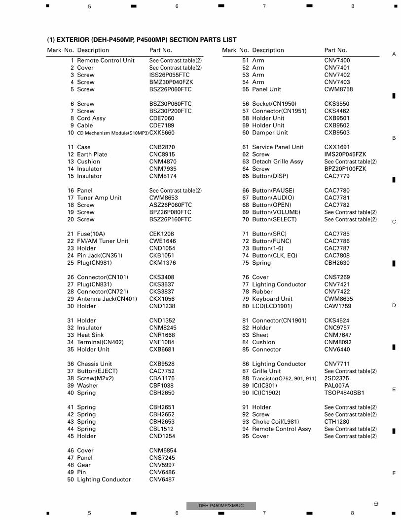
1 Remote Control Unit See Contrast table(2)2 Cover See Contrast table(2)3 Screw ISS26P055FTC4 Screw BMZ30P040FZK5 Screw BSZ26P060FTC
6 Screw BSZ30P060FTC7 Screw BSZ30P200FTC8 Cord Assy CDE70609 Cable CDE7189
10 CD Mechanism Module(S10MP3)CXK5660
11 Case CNB287012 Earth Plate CNC891513 Cushion CNM487014 Insulator CNM793515 Insulator CNM8174
16 Panel See Contrast table(2)17 Tuner Amp Unit CWM865318 Screw ASZ26P060FTC19 Screw BPZ26P080FTC20 Screw BSZ26P160FTC
21 Fuse(10A) CEK120822 FM/AM Tuner Unit CWE164623 Holder CND105424 Pin Jack(CN351) CKB105125 Plug(CN981) CKM1376
26 Connector(CN101) CKS340827 Plug(CN831) CKS353728 Connector(CN721) CKS383729 Antenna Jack(CN401) CKX105630 Holder CND1238
31 Holder CND135232 Insulator CNM824533 Heat Sink CNR166834 Terminal(CN402) VNF108435 Holder Unit CXB6681
36 Chassis Unit CXB952837 Button(EJECT) CAC775238 Screw(M2x2) CBA117639 Washer CBF103840 Spring CBH2650
41 Spring CBH265142 Spring CBH265243 Spring CBH265344 Spring CBL151245 Holder CND1254
46 Cover CNM685447 Panel CNS724548 Gear CNV599749 Pin CNV648650 Lighting Conductor CNV6487
51 Arm CNV740052 Arm CNV740153 Arm CNV740254 Arm CNV740355 Panel Unit CWM8758
56 Socket(CN1950) CKS355057 Connector(CN1951) CKS446258 Holder Unit CXB950159 Holder Unit CXB950260 Damper Unit CXB9503
61 Service Panel Unit CXX169162 Screw IMS20P045FZK63 Detach Grille Assy See Contrast table(2)64 Screw BPZ20P100FZK65 Button(DISP) CAC7779
66 Button(PAUSE) CAC778067 Button(AUDIO) CAC778168 Button(OPEN) CAC778269 Button(VOLUME) See Contrast table(2)70 Button(SELECT) See Contrast table(2)
71 Button(SRC) CAC778572 Button(FUNC) CAC778673 Button(1-6) CAC778774 Button(CLK, EQ) CAC780875 Spring CBH2630
76 Cover CNS726977 Lighting Conductor CNV742178 Rubber CNV742279 Keyboard Unit CWM863580 LCD(LCD1901) CAW1759
81 Connector(CN1901) CKS452482 Holder CNC975783 Sheet CNM764784 Cushion CNM809285 Connector CNV6440
86 Lighting Conductor CNV771187 Grille Unit See Contrast table(2)88 Transistor(Q752, 901, 911) 2SD237589 IC(IC301) PAL007A90 IC(IC1902) TSOP4840SB1
91 Holder See Contrast table(2)92 Screw See Contrast table(2)93 Choke Coil(L981) CTH128094 Remote Control Assy See Contrast table(2)95 Cover See Contrast table(2)
Mark No. Description Part No. Mark No. Description Part No.
(1) EXTERIOR (DEH-P450MP, P4500MP) SECTION PARTS LIST
10
1 2 3 4
1 2 3 4
F
E
D
C
B
A
DEH-P450MP/XM/UC
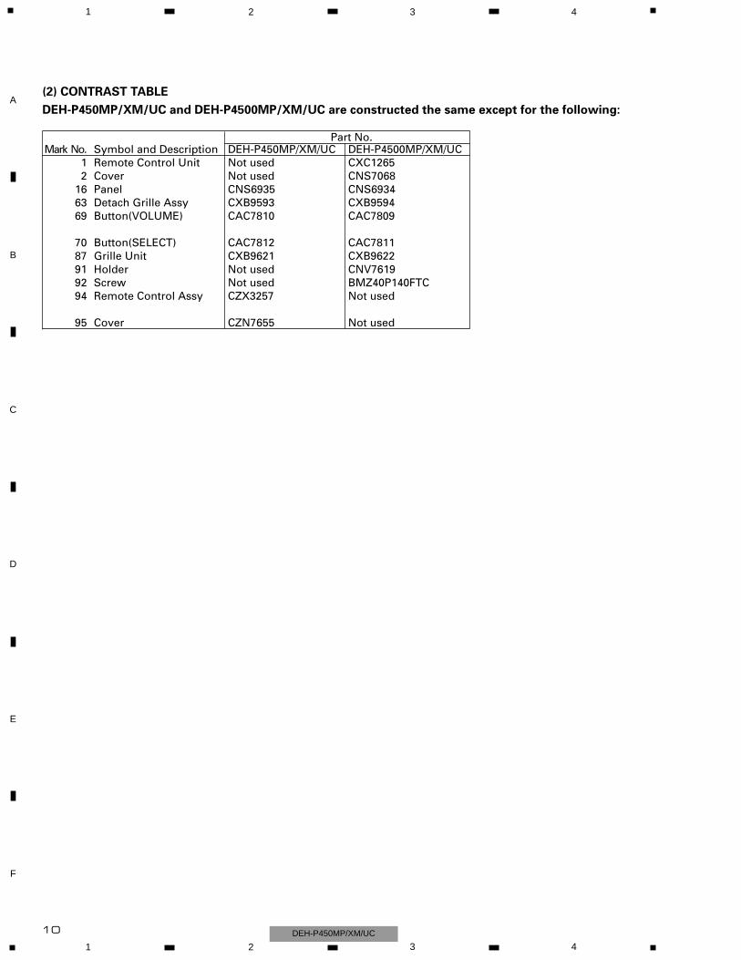
Part No.Mark No. Symbol and Description DEH-P450MP/XM/UC DEH-P4500MP/XM/UC
1 Remote Control Unit Not used CXC12652 Cover Not used CNS7068
16 Panel CNS6935 CNS693463 Detach Grille Assy CXB9593 CXB959469 Button(VOLUME) CAC7810 CAC7809
70 Button(SELECT) CAC7812 CAC781187 Grille Unit CXB9621 CXB962291 Holder Not used CNV761992 Screw Not used BMZ40P140FTC94 Remote Control Assy CZX3257 Not used
95 Cover CZN7655 Not used
(2) CONTRAST TABLE
DEH-P450MP/XM/UC and DEH-P4500MP/XM/UC are constructed the same except for the following:

11
5 6 7 8
F
E
D
C
B
A
5 6 7 8DEH-P450MP/XM/UC
12
1 2 3 4
1 2 3 4
F
E
D
C
B
A
DEH-P450MP/XM/UC
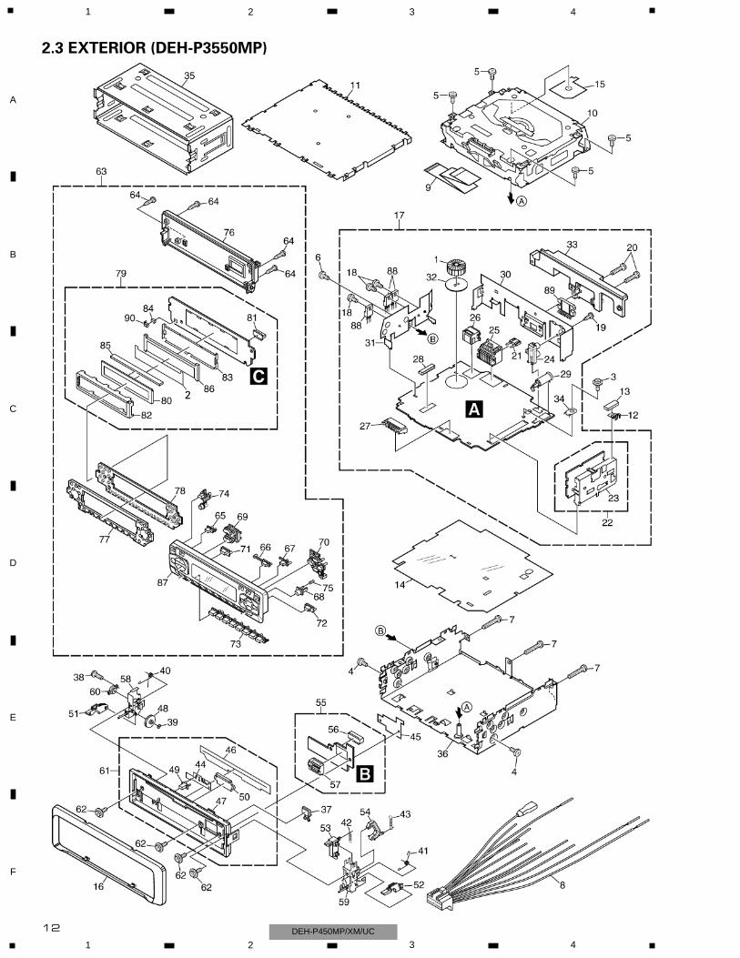
2.3 EXTERIOR (DEH-P3550MP)
13
5 6 7 8
F
E
D
C
B
A
5 6 7 8DEH-P450MP/XM/UC
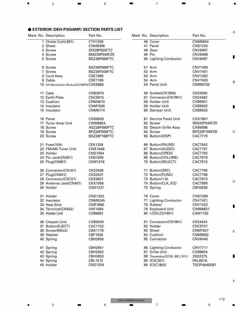
1 Choke Coil(L981) CTH12802 Sheet CNM83863 Screw ISS26P055FTC4 Screw BMZ30P040FZK5 Screw BSZ26P060FTC
6 Screw BSZ30P060FTC7 Screw BSZ30P200FTC8 Cord Assy CDE70609 Cable CDE7189
10 CD Mechanism Module(S10MP3)CXK5660
11 Case CNB287012 Earth Plate CNC891513 Cushion CNM487014 Insulator CNM793515 Insulator CNM8174
16 Panel CNS693517 Tuner Amp Unit CWM865418 Screw ASZ26P060FTC19 Screw BPZ26P080FTC20 Screw BSZ26P160FTC
21 Fuse(10A) CEK120822 FM/AM Tuner Unit CWE164623 Holder CND105424 Pin Jack(CN351) CKB105925 Plug(CN981) CKM1376
26 Connector(CN101) CKS340827 Plug(CN831) CKS353728 Connector(CN721) CKS383729 Antenna Jack(CN401) CKX105630 Holder CND1237
31 Holder CND135232 Insulator CNM824533 Heat Sink CNR166834 Terminal(CN402) VNF108435 Holder Unit CXB6681
36 Chassis Unit CXB952837 Button(EJECT) CAC775238 Screw(M2x2) CBA117639 Washer CBF103840 Spring CBH2650
41 Spring CBH265142 Spring CBH265243 Spring CBH265344 Spring CBL151245 Holder CND1254
46 Cover CNM685447 Panel CNS724548 Gear CNV599749 Pin CNV648650 Lighting Conductor CNV6487
51 Arm CNV740052 Arm CNV740153 Arm CNV740254 Arm CNV740355 Panel Unit CWM8758
56 Socket(CN1950) CKS355057 Connector(CN1951) CKS446258 Holder Unit CXB950159 Holder Unit CXB950260 Damper Unit CXB9503
61 Service Panel Unit CXX169162 Screw IMS20P045FZK63 Detach Grille Assy CXB959664 Screw BPZ20P100FZK65 Button(DISP) CAC7779
66 Button(PAUSE) CAC784267 Button(AUDIO) CAC778168 Button(OPEN) CAC778269 Button(VOLUME) CAC781070 Button(SELECT) CAC7812
71 Button(SRC) CAC778572 Button(FUNC) CAC778673 Button(1-6) CAC781374 Button(CLK, EQ) CAC780875 Spring CBH2630
76 Cover CNS726977 Lighting Conductor CNV742178 Rubber CNV742279 Keyboard Unit CWM863180 LCD(LCD1901) CAW1762
81 Connector(CN1901) CKS452482 Holder CNC975783 Sheet CNM764784 Cushion CNM809285 Connector CNV6440
86 Lighting Conductor CNV771187 Grille Unit CXB962488 Transistor(Q752, 901, 911) 2SD237589 IC(IC301) PAL007A90 IC(IC1902) TSOP4840SB1
Mark No. Description Part No. Mark No. Description Part No.
- EXTERIOR (DEH-P3550MP) SECTION PARTS LIST
14
1 2 3 4
1 2 3 4
F
E
D
C
B
A
DEH-P450MP/XM/UC
1GEM10242GEM10453GEM1035
1
1
1
1
1
1
1
1
2
2
2
2
1
1
1
1
1
2
2
1
3
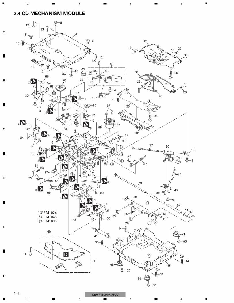
2.4 CD MECHANISM MODULE
5 6 7 8
F
E
D
C
B
A
5 6 7 8DEH-P450MP/XM/UC 15
Mark No. Description Part No. Mark No. Description Part No.
1 CD Core Unit(S10MP3) CWX27422 Connector(CN101) CKS41823 Connector(CN901) CKS40174 Screw BMZ20P035FTC5 Screw BSZ20P040FTC
6 Screw(M2x4) CBA13627 Screw(M2x3) CBA15118 Screw(M2x3) CBA15279 Washer CBF1037
10 Washer CBF1038
11 Washer CBF106012 Spring CBH239013 Spring CBH260614 Spring CBH260715 Spring CBH2608
16 Spring CBH260917 Spring CBH261018 Spring CBH261119 Spring CBH261220 Spring CBH2613
21 Spring CBH261422 Spring CBH261523 Spring CBH261624 Spring CBH261725 Spring CBH2620
26 Spring CBH262127 Spring CBH264128 Spring CBH264229 Spring CBH264330 Spring CBH2659
31 Spring CBH2688* 32 Spring CBL1614
33 Shaft CLA384534 Frame CNC996235 Frame CNC9963
36 Bracket CNC996637 Bracket CNC996738 Arm CNC996839 Arm CNC997340 Lever CNC9983
41 Lever CNC998442 Sheet CNM813443 Collar CNV690644 Guide CNV692545 Arm CNV7198
46 Rack CNV719947 Holder CNV720148 Holder CNV720249 Arm CNV720350 Gear CNV7207
51 Gear CNV720852 Gear CNV720953 Gear CNV721054 Gear CNV721155 Gear CNV7212
56 Rack CNV721457 Arm CNV721558 Arm CNV721659 Guide CNV721760 Roller CNV7218
61 Gear CNV721962 Arm CNV722163 Arm CNV722064 Arm CNV722265 Damper CNV7313
66 Damper CNV731467 Arm CNV734168 Arm CNV734269 Guide CNV736070 Guide CNV7361
71 Holder CNV743772 Arm CNV744473 Gear CNV759574 Damper CNV761875 Motor Unit(M1) CXB6007
76 Chassis Unit CXB872877 Screw Unit CXB872978 Gear Unit CXB873179 Arm Unit CXB873280 Arm Unit CXB8735
81 Arm Unit CXB885282 Motor Unit(M2) CXB893383 Bracket CNC998584 Screw JFZ20P020FTC85 Screw(M2x5) EBA1028
86 Screw JFZ20P020FTC87 Screw JGZ17P022FTC88 Washer YE15FTC89 Washer YE20FTC90 Pickup Unit(Service)(P10) CXX1641
91 Screw IMS26P030FMC
- CD MECHANISM MODULE SECTION PARTS LIST
16
1 2 3 4
1 2 3 4
F
E
D
C
B
A
DEH-P450MP/XM/UC
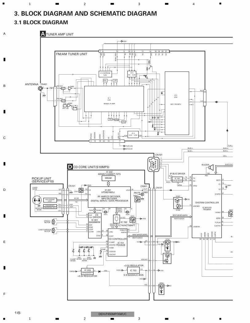
BRST,BRXEN,BSRQ
Q602
Q603
MUTE
D
CN901
Q101
M
LASERDIODE
MONITORDIODE
CLAMPSENSE
DISC SENSE
FOCUS ACT.
SPINDLEMOTOR
MCARRIAGEMOTOR
LOAD/
TRACKING ACT.
LD-
MD
FO+TO+
15
5
14
PICKUP UNIT(SERVICE)(P10)
HOLOGRAM UNIT
IC 301BA5996FM
IC 201UPD63760GJ
IC 703
+3.3V REGULATOR
RF-AMP,CD DECODER, MP3 DECODER,
DIGITAL SERVO / DATA PROCESSOR
CDDRIVER
3VDVD
3VDD
10L-OUT
5
CN101
TOP
FOP
16 SOP15 SOM18 LCOP17 LCOM
22
4,5
LOEJ
43
35LOUT
42
9CONT
12 FOP
TD/FD
AC,BD
F,E
SD/MD
1
13 TOP
HOME
12EJSENSE 8EJ
SENSE
LD+ 14
142 LD
141 PD
CD CORE UNIT(S10MP3)
3938
X201 X202
DSCSNS
CONT
LOEJ
HOME
75
77
28
26
VDD
IC 203BA033SFP
+3.3V REGULATOR
V3R3D24
CD3VON25
VDCONT24
1
S-818A33AUC-BGN
CD CONTROLLER
IC 701PE5352B
33CDMUTE
4
V3R3D
WINT,WAIT,RFOK
DRAM
IC 202MSM51V4265EP-70TS
TC74VHCT08AFTIC 702
XWINT,XWAIT,
FOK
19
1
BDATA,BSCK
VD22
Q701
17ADENA
14 VCC VDD
15
5
14
14
CLAMP93
VD2
VDCONT
ASENBO
37mute
X1
X2
PEE100
41
71
86
85
24
SYSTEM CONTROLLER
IC 601(2/2)PE5393A
CN4011
2
BUS-
BUS+
BUS+L
BUS-L
TX
RX
IPPW
sw
vd
d
BU
VDD
CN721
TUNER AMP UNIT
16X601
15
EVST,EVC
TUN L
BUS+L
BUS-L
CD L
96
DP
DT
95
KY
DT
21SYSPW
20
ILM
PW
90
ds
en
s
A
5
81
7
CN101
11
BUZZER
14
IC 101HA12187FP
IP-BUS DRIVER
1
2
8
6
5 TX
RX
IPPW
BU
Q101
Q102
TUN 3.3V
SYS 8.4V
VDD
ANTENNA
FLPILM9
ejectin8
BU
Q751
Q752
20
19
5
21
80 VDSENS
VDD
BRST,BRXEN,BSRQ
BDATA,BSCK
VD
Q754
22
VD
Q60183AVREF
22adpw
FMRF
ANT adjRF adj
FM ANT
T51 CF52CF51
RFG
ND
OS
CG
ND
DG
ND
AU
DIO
GN
D
NC
VC
C
VD
D_3
.3
3.3V 2.5VIC 4
3.3V 2.5V
←
IC 22.5V
WC
CE
2
RO
M_V
DD SL DI
CK
CE
1
NC
DO
NC
NC
NC
NC
7 6 13 5 10 9 8 11 14 18 19 20 21
1
3
2 12 15 22 16 4 17
IC 13.3V
AM ANT FMRFATT
LPFOSC
IC 3 EEPROM5.0V
IC 55V 3.3V←
ATT
MIXER, IF AMP DET, FM MPX
24
23
Rch
Lch
FM/AM TUNER UNIT
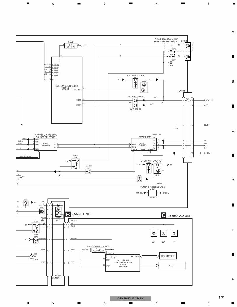
3. BLOCK DIAGRAM AND SCHEMATIC DIAGRAM
3.1 BLOCK DIAGRAM
17
5 6 7 8
F
E
D
C
B
A
5 6 7 8DEH-P450MP/XM/UC
11
1
bsens
asens
VDD
BU
92
93
10FL
11RL
37
ILB
SWVDD
ILB
SWDVDD
23
21
3
5
FL-
FL+
RL-
RL+
ACC
IN2-L3
IN4+L5
IN4-L6
IN3-L4
FLIN14
RLIN12
22 4
RESET
POWER AMP
IC 601(1/2)PE5393A
IC 131PML003AM
IC 651BD4834G
IC 301PAL007A
re
se
t
VDD
Q901
Q931
SYSPW
ELECTRONIC VOLUME/SOURCE SELECTOR
BU
VDD
STBYMUTE
IC 1901PD6340A
LCD DRIVER/KEY CONTROLLER
KEY MATRIX
9
11
KEY DATA
VD
D
55
CN1901Q961
Q962
Q971
KEYBOARD UNIT
16X601
15
2
EVST,EVCK,EVDT
TUN L
BUS+L
BUS-L
CD L
DPDT 3
5
DPDT
KYDT
SYS 8.4V BU
Q912
Q913
21
BU
Q301MUTE
Q351
7
2
11
14
7
2
11
14
CN1950CN1951
KYDT
4
2
10
8
IC 1902TSOP4840SB1
REMOTE CONTROL SENSOR
OPT IN31
17
RFM
18
20
DPDT
KTDT LCD
PANEL UNIT
MUTE
RL
S831
DSENS
SYSTEM CONTROLLER
25
B.REMOTE
VDD REGULATOR
BACKUP SENSE
ACC SENSE
SYS 8.4V REGULATOR
14
8
6
5
7
16
11
14
8
6
5
7
16
11
15 15
B C
CN981
Q502
BU
FUSE
10A
SL
TUNPCE2
TUNPCE1
TUNPDI
TUNPDO
74
32
99
94
98
TUNPCK97
CE2
CE1
BA033FP
IC 921
13SYS 8.4VTUN 3.3V
TUNER 3.3V REGULATOR
Q911
DO
DI
CK
Q902
DALMON10
BU
20
Q501
VLC
D
11
810 10 5BL+B
CN831
8 8
S1970
EJECT9 9
DGND
BU 5
6
5
6Q831
9
8
FL
RL
CN351
4
8
Q352
FL
Q60183
22
VDD
FL-FL+RL-RL+
BACK UP
GND
ACC
B.REM
DEH-P450MP/XM/UCDEH-P4500MP/XM/UC

18
1 2 3 4
1 2 3 4
F
E
D
C
B
A
DEH-P450MP/XM/UC
EJECT
DE
TAC
H S
EN
SE
R9403
0R0
R9101
0R0
FM/A
M T
UN
ER
UN
IT
CN901CD CORE UNIT(S10MP3)D
KE
YB
OA
RD
UN
ITC
CN
1901
PANEL UNITB
FM:-31AM:-31
CDIP-BUS:+2
CD:0dBs
IP-BUS:+2.2dBs
FM(30%):-30.0dBsAM(30%):-30.0dBs
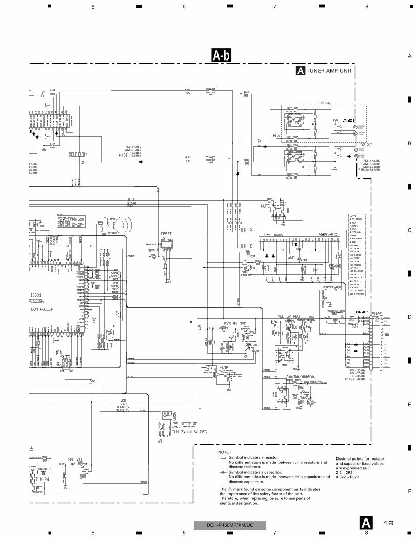
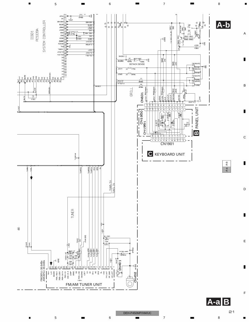
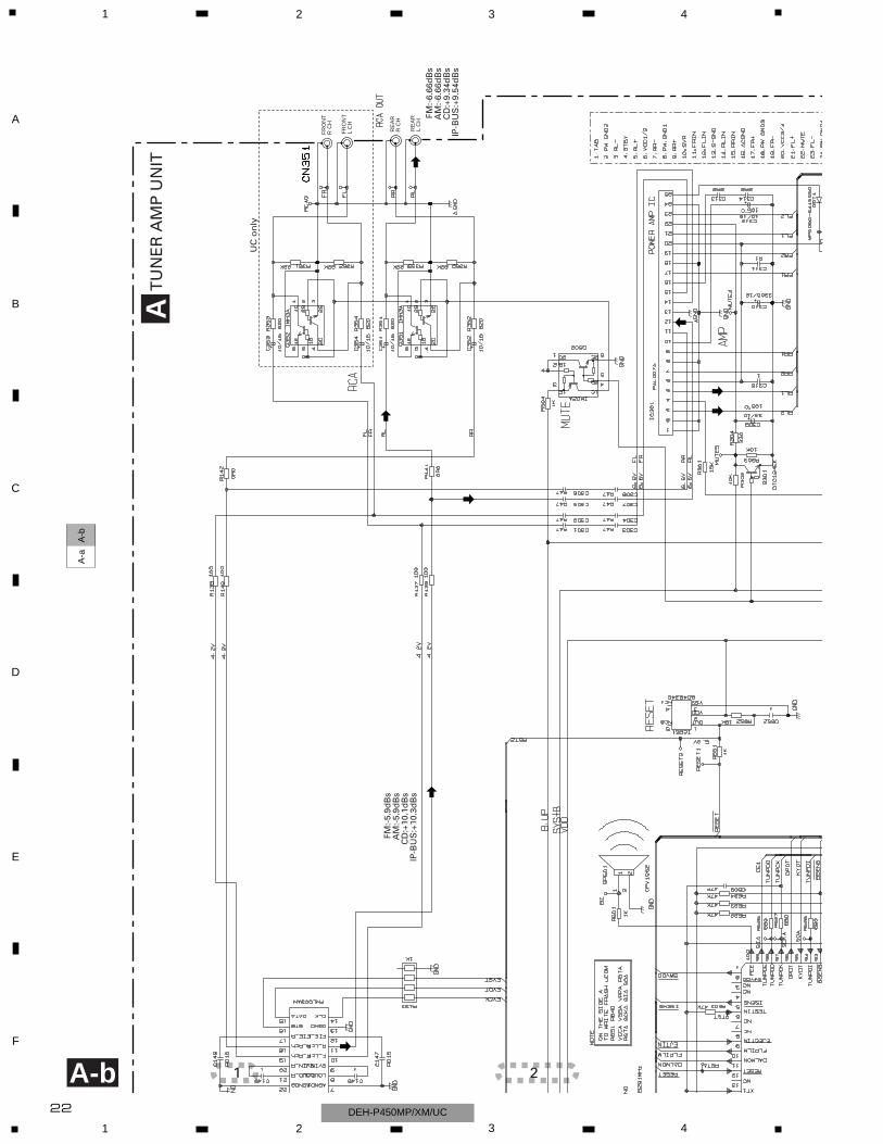
3.2 OVERALL CONNECTION DIAGRAM(GUIDE PAGE)
Note: When ordering service parts, be sure to refer to “EXPLODED VIEWS AND PARTS LIST” or “ELECTRICAL
PARTS LIST”.
A-a A-b
A-a A-b
A-b A-a
Large sizeSCH diagram
Guide page
Detailed page
A B
A-a
19
5 6 7 8
F
E
D
C
B
A
5 6 7 8DEH-P450MP/XM/UC
BACKUP
GND
RL—
RL+
FL—
FL+
B.REM
ACC
RR—
RR+
FR—
FR+
AND
600µH >
FRONTR CH
FRONTL CH
REARR CH
REARL CH
Decimal points for resistorand capacitor fixed valuesare expressed as :2.2 2R20.022 R022
← ←
The > mark found on some component parts indicatesthe importance of the safety factor of the part.Therefore, when replacing, be sure to use parts ofidentical designation.
Symbol indicates a resistor.No differentiation is made between chip resistors anddiscrete resistors.
NOTE :
Symbol indicates a capacitor.No differentiation is made between chip capacitors anddiscrete capacitors.
TUNER AMP UNITA
UCES
UC only
FM:+30dBsAM:+20dBsCD:+36dBs
IP-BUS:+36dBs
FM:-6.66dBsAM:-6.66dBsCD:+9.34dBs
IP-BUS:+9.54dBs
FM:-5.9dBsAM:-5.9dBs
CD:+10.1dBsIP-BUS:+10.3dBs
1.0dBs1.0dBsD:0dBs2.2dBs
A-b
A

20
1 2 3 4
1 2 3 4
F
E
D
C
B
A
DEH-P450MP/XM/UC
A-a
A-b
A-a
A-a
A-b 1 2
R91
01
0R0
CN
901
CD
CO
RE
UN
IT(S
10M
P3)
D
FM:-
31.0
dB
sA
M:-
31.0
dB
sC
D:0
dB
sIP
-BU
S:+
2.2d
Bs
CD
:0d
Bs
IP-B
US
:+2.
2dB
s
21
5 6 7 8
F
E
D
C
B
A
5 6 7 8DEH-P450MP/XM/UC
A-a
A-b
A-a
A-a
A-b
B
3 4
EJE
CT
DETACH SENSE
R94
03
0R0
FM/AM TUNER UNIT
KEYBOARD UNITC
CN1901
PAN
EL
UN
ITB
E
FM(3
0%):
-30.
0dB
sA
M(3
0%):
-30.
0dB
s
22
1 2 3 4
1 2 3 4
F
E
D
C
B
A
DEH-P450MP/XM/UC
A-a
A-b
A-b 1 2
FR
ON
TR
CH
FR
ON
TL
CH
RE
AR
R C
H
RE
AR
L C
H
TU
NE
R A
MP
UN
ITA
UC
on
ly
FM:-
6.66
dB
sA
M:-
6.66
dB
sC
D:+
9.34
dB
sIP
-BU
S:+
9.54
dB
s
FM:-
5.9d
Bs
AM
:-5.
9dB
sC
D:+
10.1
dB
sIP
-BU
S:+
10.3
dB
s
23
5 6 7 8
F
E
D
C
B
A
5 6 7 8DEH-P450MP/XM/UC
A-a
A-b
A-b3 4
BA
CK
UP
GN
D
RL—
RL+FL—
FL+
B.R
EM
AC
C
RR
—
RR
+
FR
—
FR
+
AND
600µ
H>
Dec
imal
po
ints
fo
r re
sist
or
and
cap
acit
or
fixe
d v
alu
esar
e ex
pre
ssed
as
:2.
2
2R2
0.02
2
R02
2
←
←
Th
e >
mar
k fo
un
d o
n s
om
e co
mp
on
ent
par
ts in
dic
ates
the
imp
ort
ance
of
the
safe
ty f
acto
r o
f th
e p
art.
Th
eref
ore
, wh
en r
epla
cin
g, b
e su
re t
o u
se p
arts
of
iden
tica
l des
ign
atio
n.
Sym
bo
l in
dic
ates
a r
esis
tor.
No
dif
fere
nti
atio
n is
mad
e b
etw
een
ch
ip r
esis
tors
an
dd
iscr
ete
resi
sto
rs.
NO
TE
: Sym
bo
l in
dic
ates
a c
apac
ito
r.N
o d
iffe
ren
tiat
ion
is m
ade
bet
wee
n c
hip
cap
acit
ors
an
dd
iscr
ete
cap
acit
ors
.
UC
ES
FM:+
30d
Bs
AM
:+20
dB
sC
D:+
36d
Bs
IP-B
US
:+36
dB
s
24
1 2 3 4
1 2 3 4
F
E
D
C
B
A
DEH-P450MP/XM/UC
3.3 KEYBOARD UNIT
C
C KEYBOARD UNIT
25
5 6 7 8
F
E
D
C
B
A
5 6 7 8DEH-P450MP/XM/UC
C
BC
N19
51
P450MPP4500MP
LCD1901 CAW1759D1801, 1802 NSSW440-9159
150
150
150
150
CE
L165
1
CE
L165
1
SM
L-31
0PT
SM
L-31
0PT
SM
L-31
0PT
SM
L-31
0PT
SM
L-31
0PT
SM
L-31
0PT
SM
L-31
0PT
SM
L-31
0PT
SM
L-31
0PT
SM
L-31
0PT
SM
L-31
0PT
SM
L-31
0PT
P3550MP
CAW1762NSSW440-2549

26
1 2 3 4
1 2 3 4
F
E
D
C
B
A
DEH-P450MP/XM/UC
R744
PICKUP UNIT(SERVICE)(P10)
6R8K
6R8K
1R8K
R75
6
100K
100P
9P
SWITCHES:CD CORE UNIT S901 : HOME SWITCH.....ON-OFF S902 : CLAMP SWITCH....ON-OFF S903 : DSCSNS SWITCH....ON-OFF S904 : 12EJ SWITCH....ON-OFF S905 : 8EJ SWITCH....ON-OFFThe underlined indicates the original switch position.
M1 CXB6007
M2 CXB8933LOADING/CARRIAGE
MOTOR
SPINDLE MOTOR
1
8
6
5
0
!
2
3
7
@
#
F
F
T
T
T
T
T
T
T
T
F
F
F
F
F
F
CS T F
CS T F
C
ST
F
F
F
T
T
S
SC
C
S
S
C
C
F
F
T
T
3.4 CD MECHANISM MODULE(GUIDE PAGE)
D
D-a
27
5 6 7 8
F
E
D
C
B
A
5 6 7 8DEH-P450MP/XM/UC
R205
R240
0R0
R209
R207
R23
9
PE5352B
MA152WA
0R0
R75
5
CD
3VO
N
4R7/25
4R7/25
D CD CORE UNIT (S10MP3)
ACN721
4
9
$
%
^
&
*
F
T
C
S
SIGNAL LINEFOCUS SERVO LINE
TRACKING SERVO LINE
CARRIAGE SERVO LINE
SPINDLE SERVO LINE
D-b
D

1 2 3 4
1 2 3 4
F
E
D
C
B
A
DEH-P450MP/XM/UC
A-a
D-b
D-a
D-a
D-b
PIC
KU
P U
NIT
(SE
RV
ICE
)(P
10)
6R8K 6R8K
1R8K
100P
9P
0
!
#
F FT T
T T
T T
T T
F F
FF
FF
C
S
T
F
C
S
T
F
FFTT
28
5 6 7 8
F
E
D
C
B
A
5 6 7 8DEH-P450MP/XM/UC
A-a
D-b
D-a
D-a
D-b1 2 3
R74
4
R756
100K
SW
ITC
HE
S:
CD
CO
RE
UN
IT S
901
: HO
ME
SW
ITC
H...
..ON
-OFF
S90
2 : C
LAM
P S
WIT
CH
....O
N-O
FF S
903
: DS
CS
NS
SW
ITC
H...
.ON
-OFF
S90
4 : 1
2EJ
SW
ITC
H...
.ON
-OFF
S90
5 : 8
EJ
SW
ITC
H...
.ON
-OFF
Th
e u
nd
erlin
ed in
dic
ates
th
e o
rig
inal
sw
itch
po
siti
on
.
M1
CX
B60
07
M2
CX
B89
33LO
AD
ING
/CA
RR
IAG
EM
OT
OR
SP
IND
LE M
OT
OR
1
8
65
2
3
7
@
C
ST
F
F F T T
S
SC
C
S S C C
29
30
1 2 3 4
1 2 3 4
F
E
D
C
B
A
DEH-P450MP/XM/UC
D-a
D-b
D-b
R20
5
R24
0
0R0
R20
9
R20
7
DC
D C
OR
E U
NIT
(S
10M
P3)
9
$ %^
F T C S
SIG
NA
L LI
NE
FOC
US
SE
RV
O L
INE
TR
AC
KIN
G S
ER
VO
LIN
E
CA
RR
IAG
E S
ER
VO
LIN
E
SP
IND
LES
ER
VO
LIN
E
31
5 6 7 8
F
E
D
C
B
A
5 6 7 8DEH-P450MP/XM/UC
D-a
D-b
D-b1 2 3
44
R239
PE
5352
B
MA
152W
A
0R0
R755
CD3VON
4R7/
25
4R7/
25
AC
N72
1
4
&*
T C S
TR
AC
KIN
G S
ER
VO
LIN
E
CA
RR
IAG
E S
ER
VO
LIN
E
SP
IND
LE S
ER
VO
LIN
E
32
1 2 3 4
1 2 3 4
F
E
D
C
B
A
DEH-P450MP/XM/UC
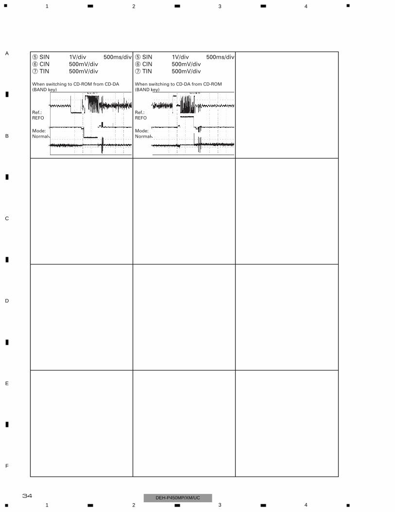
- Waveforms Note : 1. The encircled numbers denote measuring points in the circuit diagram.2. Reference voltage REFO1(1.65V)
1 DSCSNS2 CLCONT3 LOEJ4 VD
5V/div5V/div5V/div10V/div
500ms/div
When loading a 12cm CD
Ref.:GND
Mode:Normal
5 SIN6 CIN7 TIN
1V/div500mV/div500mV/div
2s/div
When setting up after loading a 12cm CD-DA disc
5 SIN6 CIN7 TIN
When setting up after loading a 12cm CD-ROM disc(1 session)
When setting up after loading a 12cm CD-ROM disc(3 session)
Ref.:REFO
Mode:Normal
1 DSCSNS2 CLCONT3 LOEJ4 VD
5V/div5V/div5V/div10V/div
500ms/div
When loading an 8cm CD
Ref.:GND
Mode:Normal
0 TE! FE
500mV/div500mV/div
200ms/div
When setting up "Source On"
Ref.:REFO
Mode:Normal
! FE8 FIN0 TE7 TIN
500mV/div500mV/div500mV/div500mV/div
20ms/div
Ref.:REFO
Mode:Normal
! FE8 FIN0 TE7 TIN
500mV/div500mV/div500mV/div500mV/div
20ms/div
During "Play"(CD-DA)During "Play"(CD-ROM)(Track Jump is generated periodically)(Refer to Track Jump waveform)
Ref.:REFO
Mode:Normal
@ MDX5 SIN
500mV/div200mV/div
50ms/div
Spindle waveform during "Play"
Ref.:REFO
Mode:Normal
# RFAGC 500mV/div 5µs/div
Ref.:REFO
Mode:Normal
@ MDX5 SIN
500mV/div1V/div
5µs/div
Spindle waveform during "Play"(Magnified) RF eye pattern
Ref.:REFO
Mode:Normal
1V/div500mV/div500mV/div
2s/div 5 SIN6 CIN7 TIN
1V/div500mV/div500mV/div
2s/div
When setting up "Source On"(12cm CD-DA)
Ref.:REFO
Mode:Normal
8 FIN9 RFOK5 SIN
200mV/div2V/div2V/div
500ms/div
Ref.:REFO
Mode:Normal
Ref.:REFO
Mode:Normal
33
5 6 7 8
F
E
D
C
B
A
5 6 7 8DEH-P450MP/XM/UC
8 FIN! FE
500mV/div500mV/div
200ms/div
Focus Search
Ref.:REFO
Mode:TEST
# RFAGC0 TE7 TIN
1V/div500mV/div500mV/div
500µs/div
Ref.:REFO
Mode:TEST
0 TE# RFAGC
500mV/div500mV/div
2ms/div
When "Tracking Open" 1 Track Jump
Ref.:REFO
Mode:TEST
# RFAGC% TE6 CIN5 SIN
1V/div1V/div500mV/div2V/div
200ms/div
Ref.:REFO
Mode:Norma
$ LRCKIN DIN
^ SCKIN
2V/div2V/div2V/div
2µs/div
Ref.:REFO
Mode:Norma
$ LRCKIN DIN
^ SCKIN
2V/div2V/div2V/div
10µs/div
Digital Audio Digital Audio(Magnified)
Ref.:GND
Mode:Norma
# RFAGC0 TE7 TIN
1V/div500mV/div500mV/div
1ms/div
32 Track Jump
Ref.:REFO
Mode:TEST
# RFAGC7 TIN0 TE8 FIN
1V/div1V/div1V/div1V/div
500µs/div
Ref.:REFO
Mode:Norma
# RFAGC0 TE7 TIN
1V/div500mV/div500mV/div
5ms/div
100 Track Jump When passing black dots(800µm)
Ref.:REFO
Mode:TEST
During inside/outside search(outer circumference → inner circumference)
& LOUT* ROUT
1V/div1V/div
200µs/div
Ref.:AGND
Mode:Norma
1 DSCSNS CLCONT
3 LOEJ
5V/div5V/div5V/div
10µs/div
Ref.:GND
Mode:Norma
1 DSCSNS
3 LOEJ
5V/div5V/div5V/div
500ms/div
When "Eject"(12cm CD)Analog Audio(sine wave, 1kHz) When "Eject"(8cm CD)
Ref.:GND
Mode:Norma
34
1 2 3 4
1 2 3 4
F
E
D
C
B
A
DEH-P450MP/XM/UC
5 SIN6 CIN7 TIN
1V/div500mV/div500mV/div
500ms/div
Ref.:REFO
Mode:Normal
5 SIN6 CIN7 TIN
1V/div500mV/div500mV/div
500ms/div
Ref.:REFO
Mode:Normal
When switching to CD-ROM from CD-DA(BAND key)
When switching to CD-DA from CD-ROM(BAND key)

35
5 6 7 8
F
E
D
C
B
A
5 6 7 8DEH-P450MP/XM/UC
36
1 2 3 4
1 2 3 4
F
E
D
C
B
A
DEH-P450MP/XM/UC
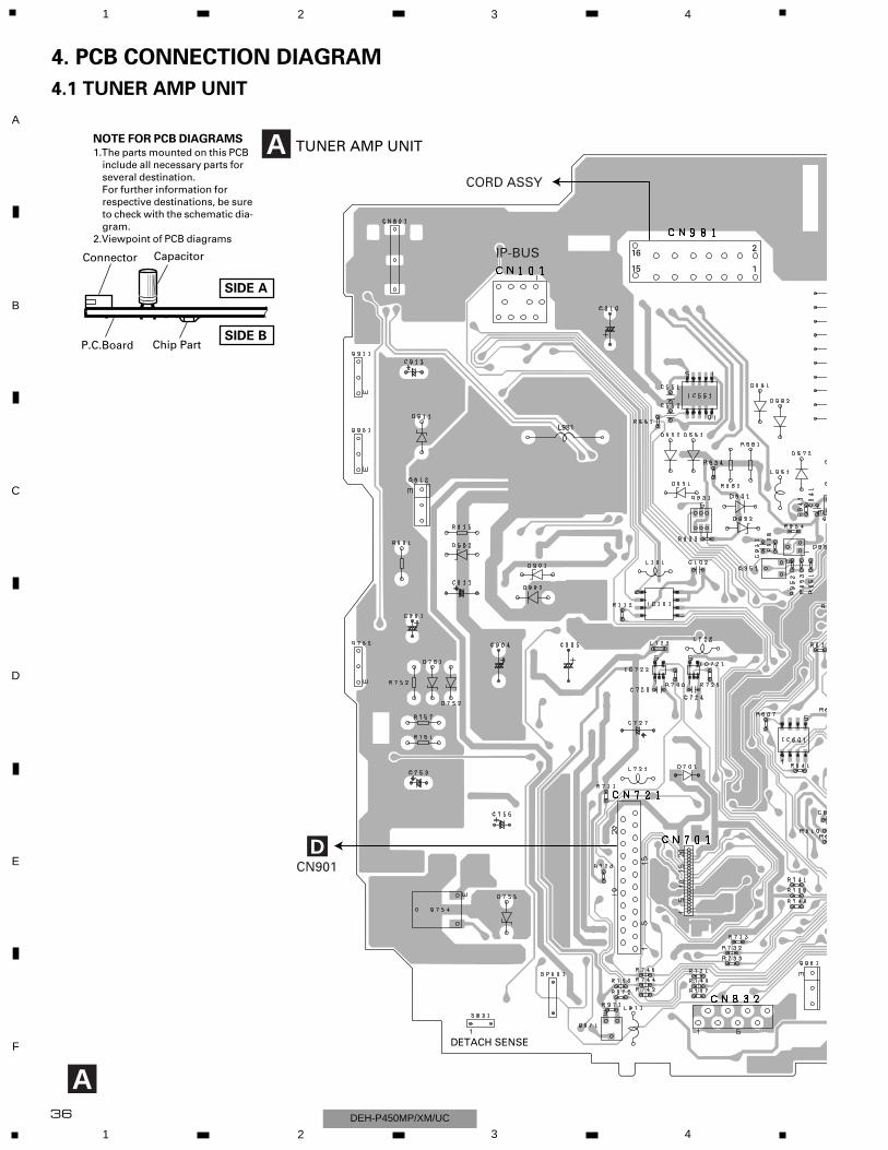
4. PCB CONNECTION DIAGRAM
4.1 TUNER AMP UNIT
CapacitorConnector
P.C.Board Chip Part
A
A TUNER AMP UNIT
SIDE B
SIDE A
NOTE FOR PCB DIAGRAMS
1.The parts mounted on this PCB include all necessary parts for several destination. For further information for respective destinations, be sure to check with the schematic dia- gram.2.Viewpoint of PCB diagrams
IP-BUS
CORD ASSY
L981
DCN901
DETACH SENSE
1
2
15
16
37
5 6 7 8
F
E
D
C
B
A
5 6 7 8DEH-P450MP/XM/UC
A
SIDE A
IC,Q
RCA OUT
ANTENNA
FM/A
M T
UN
ER
UN
IT
B CN1950
FRONT

38
1 2 3 4
1 2 3 4
F
E
D
C
B
A
DEH-P450MP/XM/UC
A
A TUNER AMP UNITIC,Q
1 1

39
5 6 7 8
F
E
D
C
B
A
5 6 7 8DEH-P450MP/XM/UC
A
SIDE B
1
40
1 2 3 4
1 2 3 4
F
E
D
C
B
A
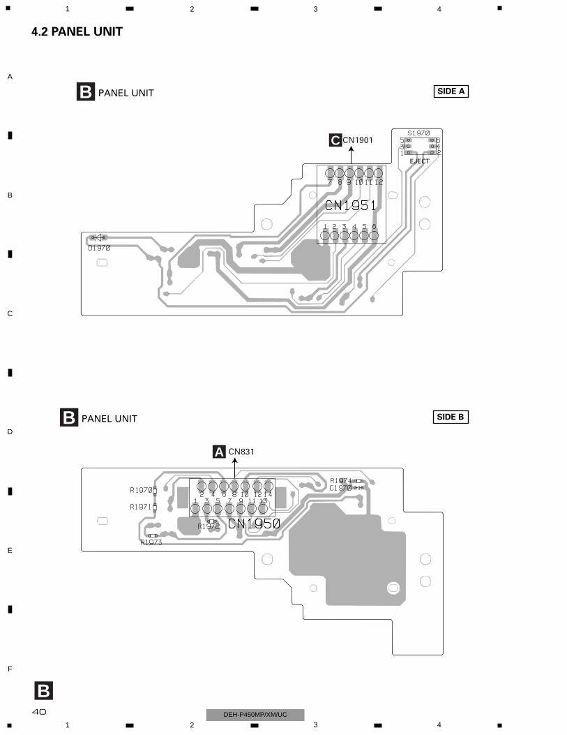
DEH-P450MP/XM/UC
B
B PANEL UNIT
B PANEL UNIT
SIDE A
SIDE B
C CN1901
A CN831
EJECT
4.2 PANEL UNIT

41
C
C KEYBOARD UNIT C KEYBOARD UNITSIDE A SIDE B
IC,QIC,Q
B CN1951C
LK
DIS
P
SR
C6
LOU
DB
AN
D/E
SC
FUN
C
PA
US
EA
UD
IO
12
34
5
EQ
↓ ↓
↓ ↓
↓
↓
5 6 7 8
F
E
D
C
B
A
5 6 7 8DEH-P450MP/XM/UC
4.3 KEYBOARD UNIT
42
1 2 3 4
1 2 3 4
F
E
D
C
B
A
DEH-P450MP/XM/UC
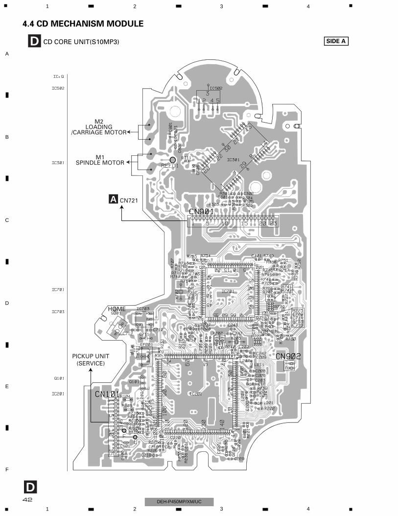
4.4 CD MECHANISM MODULE
D
D CD CORE UNIT(S10MP3) SIDE A
PICKUP UNIT(SERVICE)
HOME
M1SPINDLE MOTOR
M2LOADING
/CARRIAGE MOTOR
A CN721

43
5 6 7 8
F
E
D
C
B
A
5 6 7 8DEH-P450MP/XM/UC
D
D CD CORE UNIT(S10MP3) SIDE B
CLAMP
DSCSNS
8EJ 12EJ
44
1 2 3 4
1 2 3 4
F
E
D
C
B
A
DEH-P450MP/XM/UC
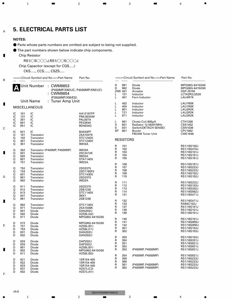
5. ELECTRICAL PARTS LIST
NOTES:
- Parts whose parts numbers are omitted are subject to being not supplied.
- The part numbers shown below indicate chip components.
Chip Resistor
RS1/_S___J,RS1/__S___J
Chip Capacitor (except for CQS.....)
CKS....., CCS....., CSZS.....
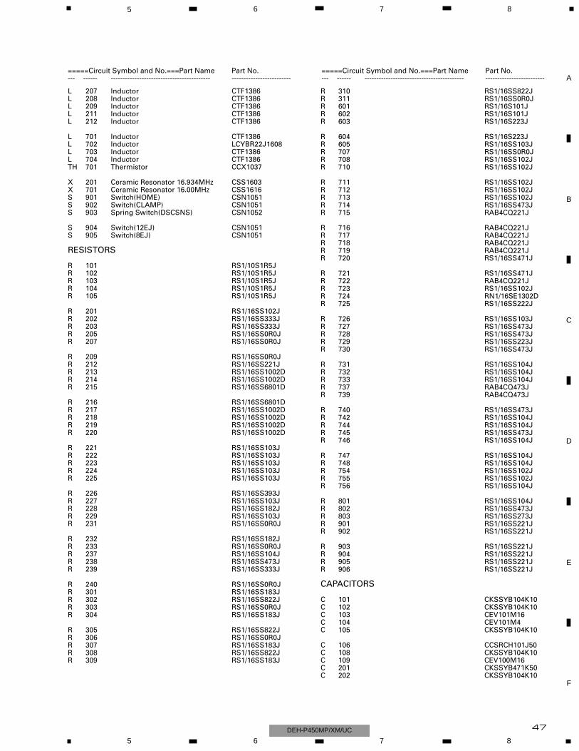
=====Circuit Symbol and No.===Part Name Part No.--- ------ ------------------------------------------ -------------------------
Unit Number : CWM8653(P450MP/XM/UC, P4500MP/XM/UC)
: CWM8654(P3550MP/XM/ES)
Unit Name : Tuner Amp Unit
MISCELLANEOUS
IC 101 IC HA12187FPIC 131 IC PML003AMIC 301 IC PAL007AIC 601 IC PE5393AIC 651 IC BD4834G
IC 921 IC BA033FPQ 101 Transistor 2SA1037KQ 102 Transistor DTC124EKQ 301 Transistor DTC124EKQ 351 Transistor IMH3A
Q 352 Transistor (P450MP, P4500MP) IMH3AQ 501 Transistor 2SC2412KQ 502 Transistor IMD2AQ 601 Transistor DTA114EKQ 751 Transistor IMD2A
Q 752 Transistor 2SD2375Q 754 Transistor 2SD1760F5Q 831 Transistor DTC143EKQ 901 Transistor 2SD2375Q 902 Transistor IMD2A
Q 911 Transistor 2SD2375Q 912 Transistor 2SB1238Q 913 Transistor DTC114EKQ 931 Transistor IMX1Q 961 Transistor 2SB1238
Q 962 Transistor DTC114EKQ 971 Transistor 2SA1036KD 501 Diode DAN202UD 502 Diode HZS9L(A2)D 571 Diode MPG06G-6415G50
D 572 Diode MPG06G-6415G50D 751 Diode HZS9L(B1)D 753 Diode HZS6L(C1)D 831 Diode DAN202UD 832 Diode DAN202U
D 833 Diode DAP202UD 834 Diode DAP202UD 901 Diode HZS6L(B1)D 902 Diode MPG06G-6415G50D 911 Diode HZS9L(B3)
D 921 Diode 1SR154-400D 922 Diode 1SR154-400D 923 Diode 1SR154-400D 931 Diode HZS7L(C3)D 932 Diode HZS7L(A1)
D 981 Diode MPG06G-6415G50D 982 Diode MPG06G-6415G50ZNR 401 Arrester DSP-201ML 131 Inductor LCTA2R2J2520L 401 Ferri-Inductor LAU4R7K
L 402 Inductor LAU1R0KL 404 Inductor LAU1R0KL 601 Inductor LAU2R2KL 721 Inductor LAU2R2KL 971 Inductor LAU2R2K
L 981 Choke Coil 600µH CTH1280X 601 Radiator 12.58291MHz CSS1402S 831 Switch(DETACH SENSE) CSN1039SP 601 Buzzer CPV1062
FM/AM Tuner Unit CWE1646
RESISTORS
R 101 RS1/16S150JR 102 RS1/16S470JR 103 RS1/16S101JR 104 RS1/16S101JR 105 RS1/16S181J
R 106 RS1/16S181JR 107 RS1/16S223JR 108 RS1/16S223JR 109 RS1/16S102JR 110 RS1/16S102J
R 111 RS1/16S222JR 112 RS1/16S103JR 113 RS1/16S332JR 114 RS1/16S562JR 131 RS1/16S471J
R 132 RS1/16S471JR 133 RAB4C102JR 137 RS1/16S101JR 138 RS1/16S101JR 139 RS1/16S101J
R 140 RS1/16S101JR 141 RS1/16S0R0JR 142 RS1/16S0R0JR 301 RS1/16S153JR 302 RS1/16S103J
R 303 RS1/16S103JR 304 RS1/16S331JR 351 RS1/16S821JR 352 RS1/16S821JR 353 (P450MP, P4500MP) RS1/16S821J
R 354 (P450MP, P4500MP) RS1/16S821JR 359 RS1/16S223JR 360 RS1/16S223JR 361 (P450MP, P4500MP) RS1/16S223JR 362 (P450MP, P4500MP) RS1/16S223J
=====Circuit Symbol and No.===Part Name Part No.--- ------ ------------------------------------------ -------------------------
A
45
5 6 7 8
F
E
D
C
B
A
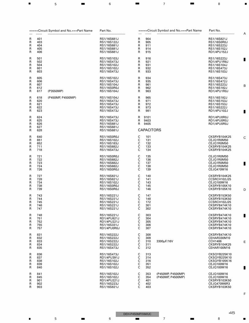
5 6 7 8DEH-P450MP/XM/UC
R 401 RS1/16S681JR 403 RS1/16S122JR 404 RS1/16S681JR 405 RS1/16S681JR 406 RS1/16S681J
R 501 RS1/16S103JR 502 RS1/16S473JR 504 RS1/16S102JR 601 RS1/16S102JR 603 RS1/16S473J
R 605 RS1/16S102JR 606 RS1/16S473JR 607 RS1/16S104JR 612 RS1/16S0R0JR 617 (P3550MP) RS1/16S104J
R 618 (P450MP, P4500MP) RS1/16S104JR 620 RS1/16S473JR 621 RS1/16S473JR 622 RS1/16S473JR 623 RS1/16S473J
R 624 RS1/16S473JR 625 RS1/16S473JR 626 RS1/16S681JR 627 RS1/16S681JR 628 RS1/16S681J
R 640 RS1/16S0R0JR 651 RS1/16S102JR 652 RS1/16S183JR 711 RS1/16S682JR 718 RS1/16S473J
R 721 RS1/16S0R0JR 722 RS1/16S682JR 723 RS1/16S682JR 724 RS1/16S682JR 726 RS1/16S0R0J
R 727 RS1/16S821JR 728 RS1/16S821JR 734 RS1/16S102JR 738 RS1/16S0R0JR 739 RS1/16S0R0J
R 743 RS1/16S221JR 744 RS1/16S221JR 745 RS1/16S221JR 746 RS1/16S221JR 747 RS1/16S221J
R 748 RS1/16S221JR 751 RD1/4PU821JR 752 RD1/4PU221JR 755 RS1/16S331JR 757 RD1/4PU0R0J
R 831 RS1/16S222JR 832 RS1/16S222JR 833 RS1/16S222JR 834 RS1/16S222JR 835 RS1/16S473J
R 836 RS1/16S473JR 837 RD1/4PU391JR 838 RS1/16S102JR 839 RS1/16S102JR 840 RS1/16S102J
R 841 RS1/16S102JR 845 RS1/16S102JR 901 RD1/4PU221JR 902 RS1/16S223JR 903 RS1/16S821J
R 904 RS1/16S821JR 905 RS1/16S0R0JR 911 RS1/16S223JR 914 RS1/16S152JR 915 RD1/4PU152J
R 916 RS1/16S223JR 921 RD1/4PU1R8JR 931 RS1/16S104JR 932 RS1/16S473JR 933 RS1/16S103J
R 934 RS1/16S473JR 935 RS1/16S472JR 961 RS1/16S223JR 962 RS1/16S182JR 963 RD1/4PU1R0J
R 965 RS1/16S182JR 971 RS1/16S153JR 972 RS1/16S153JR 973 RS1/16S222JR 981 RD1/4PU102J
R 9101 RD1/4PU0R0JR 9403 RD1/4PU0R0JR 9405 RD1/4PU0R0J
CAPACITORS
C 101 CKSRYB104K25C 131 CEJQ1R0M50C 132 CEJQ1R0M50C 133 CKSRYB104K25C 134 CKSRYB104K25
C 135 CEJQ1R0M50C 136 CEJQ1R0M50C 137 CEJQ1R0M50C 138 CEJQ1R0M50C 139 CEJQ470M16
C 140 CKSRYB104K25C 141 CCSRCH102J25C 143 CEJQ100M16C 145 CKSRYB105K10C 146 CKSRYB105K10
C 147 CKSRYB153K50C 148 CKSRYB153K50C 172 CCSRCH102J25C 301 CKSRYB474K10C 302 CKSRYB474K10
C 303 CKSRYB474K10C 304 CKSRYB474K10C 305 CKSRYB474K10C 306 CKSRYB474K10C 307 CKSRYB474K10
C 308 CKSRYB474K10C 309 CEHAR330M10C 310 3300µF/16V CCH1486C 311 CKSRYB104K25C 312 CEHAR100M16
C 313 CKSQYB225K10C 314 CKSQYB225K10C 316 CKSQYB105K16C 351 CEJQ100M16C 352 CEJQ100M16
C 353 (P450MP, P4500MP) CEJQ100M16C 354 (P450MP, P4500MP) CEJQ100M16C 401 CKSRYB103K50C 402 CEJQ470M6R3C 403 CKSRYB103K50
=====Circuit Symbol and No.===Part Name Part No.--- ------ ------------------------------------------ -------------------------
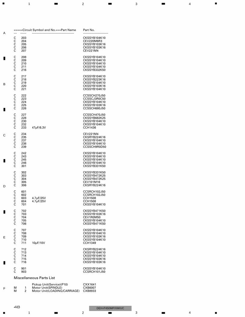
=====Circuit Symbol and No.===Part Name Part No.--- ------ ------------------------------------------ -------------------------
46
1 2 3 4
1 2 3 4
F
E
D
C
B
A
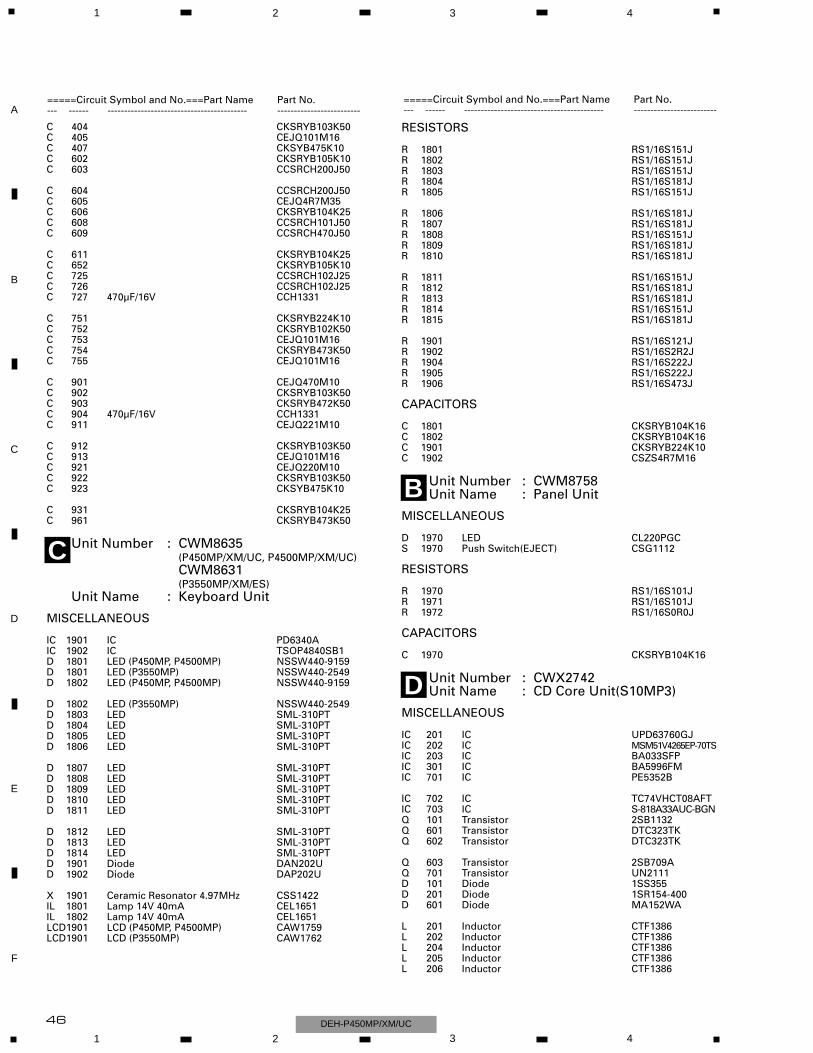
DEH-P450MP/XM/UC
C 404 CKSRYB103K50C 405 CEJQ101M16C 407 CKSYB475K10C 602 CKSRYB105K10C 603 CCSRCH200J50
C 604 CCSRCH200J50C 605 CEJQ4R7M35C 606 CKSRYB104K25C 608 CCSRCH101J50C 609 CCSRCH470J50
C 611 CKSRYB104K25C 652 CKSRYB105K10C 725 CCSRCH102J25C 726 CCSRCH102J25C 727 470µF/16V CCH1331
C 751 CKSRYB224K10C 752 CKSRYB102K50C 753 CEJQ101M16C 754 CKSRYB473K50C 755 CEJQ101M16
C 901 CEJQ470M10C 902 CKSRYB103K50C 903 CKSRYB472K50C 904 470µF/16V CCH1331C 911 CEJQ221M10
C 912 CKSRYB103K50C 913 CEJQ101M16C 921 CEJQ220M10C 922 CKSRYB103K50C 923 CKSYB475K10
C 931 CKSRYB104K25C 961 CKSRYB473K50
Unit Number : CWM8635(P450MP/XM/UC, P4500MP/XM/UC)CWM8631(P3550MP/XM/ES)
Unit Name : Keyboard Unit
MISCELLANEOUS
IC 1901 IC PD6340AIC 1902 IC TSOP4840SB1D 1801 LED (P450MP, P4500MP) NSSW440-9159D 1801 LED (P3550MP) NSSW440-2549D 1802 LED (P450MP, P4500MP) NSSW440-9159
D 1802 LED (P3550MP) NSSW440-2549D 1803 LED SML-310PTD 1804 LED SML-310PTD 1805 LED SML-310PTD 1806 LED SML-310PT
D 1807 LED SML-310PTD 1808 LED SML-310PTD 1809 LED SML-310PTD 1810 LED SML-310PTD 1811 LED SML-310PT
D 1812 LED SML-310PTD 1813 LED SML-310PTD 1814 LED SML-310PTD 1901 Diode DAN202UD 1902 Diode DAP202U
X 1901 Ceramic Resonator 4.97MHz CSS1422IL 1801 Lamp 14V 40mA CEL1651IL 1802 Lamp 14V 40mA CEL1651LCD1901 LCD (P450MP, P4500MP) CAW1759LCD1901 LCD (P3550MP) CAW1762
RESISTORS
R 1801 RS1/16S151JR 1802 RS1/16S151JR 1803 RS1/16S151JR 1804 RS1/16S181JR 1805 RS1/16S151J
R 1806 RS1/16S181JR 1807 RS1/16S181JR 1808 RS1/16S151JR 1809 RS1/16S181JR 1810 RS1/16S181J
R 1811 RS1/16S151JR 1812 RS1/16S181JR 1813 RS1/16S181JR 1814 RS1/16S151JR 1815 RS1/16S181J
R 1901 RS1/16S121JR 1902 RS1/16S2R2JR 1904 RS1/16S222JR 1905 RS1/16S222JR 1906 RS1/16S473J
CAPACITORS
C 1801 CKSRYB104K16C 1802 CKSRYB104K16C 1901 CKSRYB224K10C 1902 CSZS4R7M16
Unit Number : CWM8758Unit Name : Panel Unit
MISCELLANEOUS
D 1970 LED CL220PGCS 1970 Push Switch(EJECT) CSG1112
RESISTORS
R 1970 RS1/16S101JR 1971 RS1/16S101JR 1972 RS1/16S0R0J
CAPACITORS
C 1970 CKSRYB104K16
Unit Number : CWX2742Unit Name : CD Core Unit(S10MP3)
MISCELLANEOUS
IC 201 IC UPD63760GJIC 202 IC MSM51V4265EP-70TSIC 203 IC BA033SFPIC 301 IC BA5996FMIC 701 IC PE5352B
IC 702 IC TC74VHCT08AFTIC 703 IC S-818A33AUC-BGNQ 101 Transistor 2SB1132Q 601 Transistor DTC323TKQ 602 Transistor DTC323TK
Q 603 Transistor 2SB709AQ 701 Transistor UN2111D 101 Diode 1SS355D 201 Diode 1SR154-400D 601 Diode MA152WA
L 201 Inductor CTF1386L 202 Inductor CTF1386L 204 Inductor CTF1386L 205 Inductor CTF1386L 206 Inductor CTF1386
=====Circuit Symbol and No.===Part Name Part No.--- ------ ------------------------------------------ -------------------------
=====Circuit Symbol and No.===Part Name Part No.--- ------ ------------------------------------------ -------------------------
C
B
D
47
5 6 7 8
F
E
D
C
B
A
5 6 7 8DEH-P450MP/XM/UC
L 207 Inductor CTF1386L 208 Inductor CTF1386L 209 Inductor CTF1386L 211 Inductor CTF1386L 212 Inductor CTF1386
L 701 Inductor CTF1386L 702 Inductor LCYBR22J1608L 703 Inductor CTF1386L 704 Inductor CTF1386TH 701 Thermistor CCX1037
X 201 Ceramic Resonator 16.934MHz CSS1603X 701 Ceramic Resonator 16.00MHz CSS1616S 901 Switch(HOME) CSN1051S 902 Switch(CLAMP) CSN1051S 903 Spring Switch(DSCSNS) CSN1052
S 904 Switch(12EJ) CSN1051S 905 Switch(8EJ) CSN1051
RESISTORS
R 101 RS1/10S1R5JR 102 RS1/10S1R5JR 103 RS1/10S1R5JR 104 RS1/10S1R5JR 105 RS1/10S1R5J
R 201 RS1/16SS102JR 202 RS1/16SS333JR 203 RS1/16SS333JR 205 RS1/16SS0R0JR 207 RS1/16SS0R0J
R 209 RS1/16SS0R0JR 212 RS1/16SS221JR 213 RS1/16SS1002DR 214 RS1/16SS1002DR 215 RS1/16SS6801D
R 216 RS1/16SS6801DR 217 RS1/16SS1002DR 218 RS1/16SS1002DR 219 RS1/16SS1002DR 220 RS1/16SS1002D
R 221 RS1/16SS103JR 222 RS1/16SS103JR 223 RS1/16SS103JR 224 RS1/16SS103JR 225 RS1/16SS103J
R 226 RS1/16SS393JR 227 RS1/16SS103JR 228 RS1/16SS182JR 229 RS1/16SS103JR 231 RS1/16SS0R0J
R 232 RS1/16SS182JR 233 RS1/16SS0R0JR 237 RS1/16SS104JR 238 RS1/16SS473JR 239 RS1/16SS333J
R 240 RS1/16SS0R0JR 301 RS1/16SS183JR 302 RS1/16SS822JR 303 RS1/16SS0R0JR 304 RS1/16SS183J
R 305 RS1/16SS822JR 306 RS1/16SS0R0JR 307 RS1/16SS183JR 308 RS1/16SS822JR 309 RS1/16SS183J
R 310 RS1/16SS822JR 311 RS1/16SS0R0JR 601 RS1/16S101JR 602 RS1/16S101JR 603 RS1/16S223J
R 604 RS1/16S223JR 605 RS1/16SS103JR 707 RS1/16SS0R0JR 708 RS1/16SS102JR 710 RS1/16SS102J
R 711 RS1/16SS102JR 712 RS1/16SS102JR 713 RS1/16SS102JR 714 RS1/16SS473JR 715 RAB4CQ221J
R 716 RAB4CQ221JR 717 RAB4CQ221JR 718 RAB4CQ221JR 719 RAB4CQ221JR 720 RS1/16SS471J
R 721 RS1/16SS471JR 722 RAB4CQ221JR 723 RS1/16SS102JR 724 RN1/16SE1302DR 725 RS1/16SS222J
R 726 RS1/16SS103JR 727 RS1/16SS473JR 728 RS1/16SS473JR 729 RS1/16SS223JR 730 RS1/16SS473J
R 731 RS1/16SS104JR 732 RS1/16SS104JR 733 RS1/16SS104JR 737 RAB4CQ473JR 739 RAB4CQ473J
R 740 RS1/16SS473JR 742 RS1/16SS104JR 744 RS1/16SS104JR 745 RS1/16SS473JR 746 RS1/16SS104J
R 747 RS1/16SS104JR 748 RS1/16SS104JR 754 RS1/16SS102JR 755 RS1/16SS102JR 756 RS1/16SS104J
R 801 RS1/16SS104JR 802 RS1/16SS473JR 803 RS1/16SS273JR 901 RS1/16SS221JR 902 RS1/16SS221J
R 903 RS1/16SS221JR 904 RS1/16SS221JR 905 RS1/16SS221JR 906 RS1/16SS221J
CAPACITORS
C 101 CKSSYB104K10C 102 CKSSYB104K10C 103 CEV101M16C 104 CEV101M4C 105 CKSSYB104K10
C 106 CCSRCH101J50C 108 CKSSYB104K10C 109 CEV100M16C 201 CKSSYB471K50C 202 CKSSYB104K10
=====Circuit Symbol and No.===Part Name Part No.--- ------ ------------------------------------------ -------------------------
=====Circuit Symbol and No.===Part Name Part No.--- ------ ------------------------------------------ -------------------------
48
1 2 3 4
1 2 3 4
F
E
D
C
B
A
DEH-P450MP/XM/UC
C 203 CKSSYB104K10C 204 CEV220M6R3C 205 CKSSYB103K16C 206 CKSSYB103K16C 207 CEV221M4
C 208 CKSSYB104K10C 209 CKSSYB104K10C 210 CKSSYB104K10C 211 CKSSYB104K10C 216 CKSSYB332K50
C 217 CKSSYB104K10C 218 CKSSYB223K16C 219 CKSSYB104K10C 220 CKSSYB103K16C 221 CKSSYB104K10
C 222 CCSSCH270J50C 223 CCSSCJ3R0C50C 224 CKSSYB104K10C 225 CKSSYB103K16C 226 CCSSCH680J50
C 227 CCSSCH470J50C 228 CKSSYB682K25C 230 CKSSYB104K10C 232 CKSSYB104K10C 233 47µF/6.3V CCH1436
C 234 CEV221M4C 235 CKSRYB224K16C 237 CKSSYB104K10C 238 CKSSYB104K10C 239 CCSSCH9R0D50
C 242 CKSSYB104K10C 243 CKSSYB104K10C 245 CKSSYB104K10C 246 CKSSYB104K10C 301 CKSSYB331K50
C 302 CKSSYB331K50C 303 CKSSYB472K25C 304 CKSSYB472K25C 305 CEV101M16C 306 CKSRYB224K16
C 601 CCSRCH102J50C 602 CCSRCH102J50C 603 4.7µF/25V CCH1508C 604 4.7µF/25V CCH1508C 701 CKSSYB104K10
C 702 CKSSYB471K50C 703 CKSSYB103K16C 704 CEV1R0M50C 705 CKSSYB104K10C 706 CKSSYB471K50
C 707 CKSSYB104K10C 708 CKSSYB104K10C 709 CKSSYB103K16C 710 CKSSYB104K10C 711 10µF/10V CCH1349
C 712 CKSRYB224K16C 713 CKSSYB104K10C 714 CKSSYB104K10C 715 CKSSYB103K16C 716 CKSSYB103K16
C 901 CKSSYB104K10C 903 CCSRCH101J50
Miscellaneous Parts List
Pickup Unit(Service)(P10) CXX1641M 1 Motor Unit(SPINDLE) CXB6007M 2 Motor Unit(LOADING/CARRIAGE) CXB8933
=====Circuit Symbol and No.===Part Name Part No.--- ------ ------------------------------------------ -------------------------
49
5 6 7 8
F
E
D
C
B
A
5 6 7 8DEH-P450MP/XM/UC
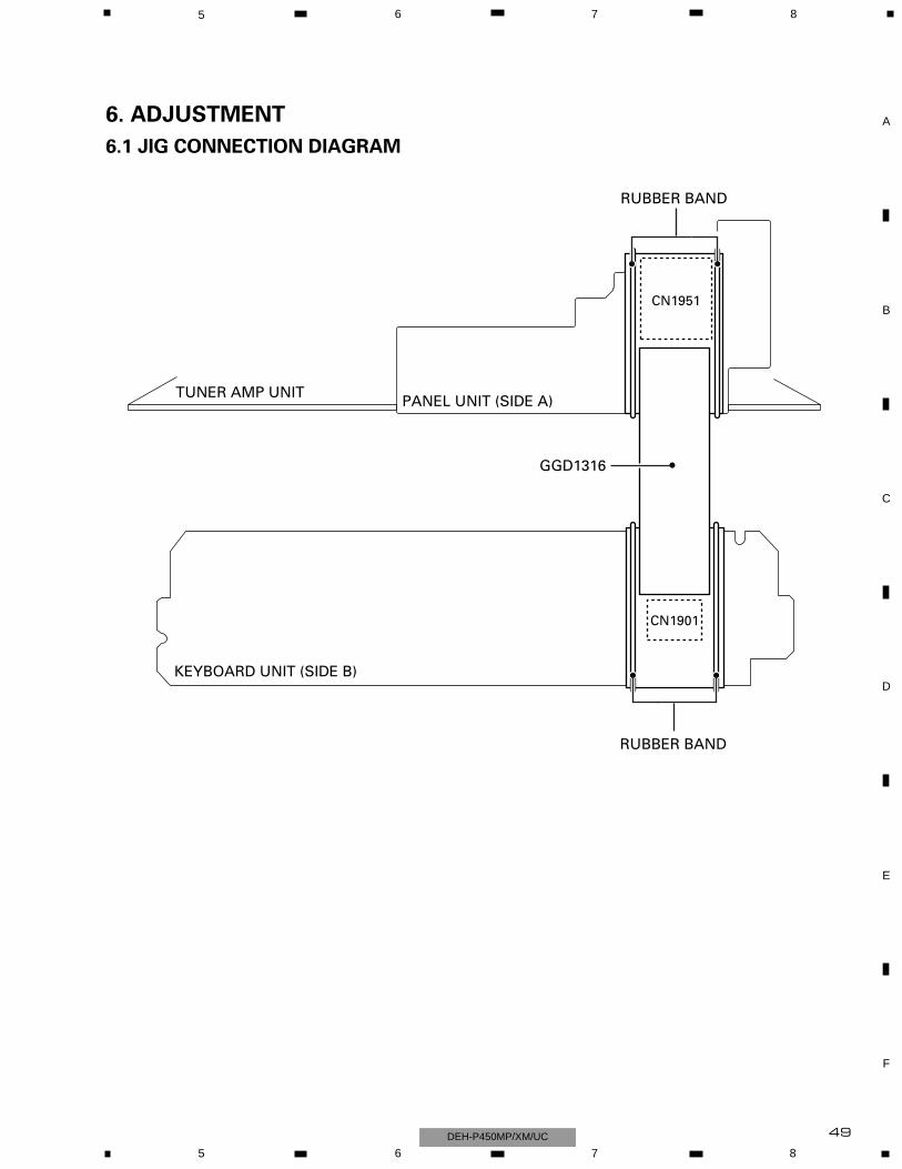
6. ADJUSTMENT
6.1 JIG CONNECTION DIAGRAM
KEYBOARD UNIT (SIDE B)
CN1951
CN1901
PANEL UNIT (SIDE A)TUNER AMP UNIT
GGD1316
RUBBER BAND
RUBBER BAND
50
1 2 3 4
1 2 3 4
F
E
D
C
B
A
DEH-P450MP/XM/UC
1) Cautions on adjustments• In this product the single voltage (3.3V) is used for the regulator. The reference voltage is the REFO1 (1.65V) instead of the GND.If you should mistakenly short the REFO1 with the GND during adjustment, accurate voltage will not be obtained, and the servo’s misoperation will apply excessive shock to the pickup. To avoid such problems:a. Do not mix up the REFO1 with the GND when connecting the (-) probe of measuring instruments. Especially on an oscilloscope, avoid connecting the (-) probe for CH1 to the GND. b. In many cases, measuring instruments have the same potential as that for the (-) probe. Be sure to set the measuring instruments to the floating state.c. If you have mistakenly connected the REFO1 to the GND, turn off the regulator or the power immediately.
• Before mounting and removing filters or leads for adjustment, be sure to turn off the regulator.
• For stable circuit operation, keep the mechanism operating for about one minute or more after the regulator is turned on.
• In the test mode, any software protections will not work. Avoid applying any mechanical or electrical shock to the mechanism during adjustment.
• The RFI and RFO signals with a wide frequency range are easy to oscillate. When observing the signals, insert a resistor of 1k ohms in series.
• The load and eject operation is not guarantied with the mechanism upside down. If the mechanism is blocked due to mistaken eject operation, reset the product or turn off and on the ACC to restore it.
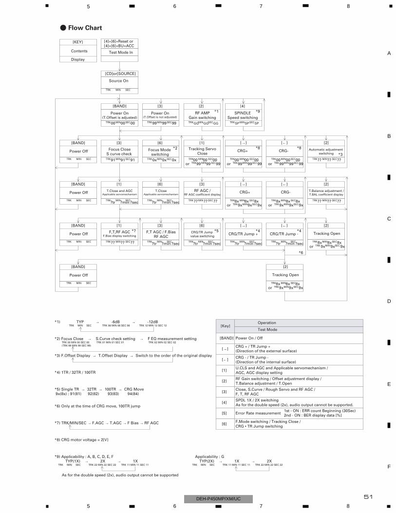
2) Test modeThis mode is used to adjust the CD mechanism module.• To enter the test mode.While pressing the 4 and 6 keys at the same time, reset.• To exit from the test mode.Turn off the ACC and back up.
Notes:a. During ejection, do not press any other keys than the EJECT key until the loaded disc is ejected.b. If you have pressed the (→) key or (←) key during focus search, turn off the power immediately to protect the actuator from damage caused by the lens stuck.c. For the TR jump modes except 100TR, the track jump operation will continue even if the key is released.d. For the CRG move and 100TR jump modes, the tracking loop will be closed at the same time when the key is released.e. When the power is turned off and on, the jump mode is reset to the single TR (91), the RF amp gain is set to 0dB, and the auto-adjustment values are reset to the default settings.
6.2 CD ADJUSTMENT
51
5 6 7 8
F
E
D
C
B
A
5 6 7 8DEH-P450MP/XM/UC
[BAND]
[BAND]
[BAND]
[BAND]
[BAND]
Power On(T.Offset is adjusted)
TRK00 MIN00 SEC
SEC
00
[CD]or[SOURCE]
Source On
TRK MIN
[4]+[6]+Reset or [4]+[6]+BU+ACC
Test Mode In
[3]
[1]
[1]
Power On(T.Offset is not adjusted)
TRK99 MIN99 SEC99
[2]
[2]
[2]
[2]
Power Off
TRK MIN SEC
Power Off
TRK MIN SEC
Power Off
TRK MIN SEC
Power Off
TRK MIN SEC
Focus CloseS curve check
T.Close and AGCApplicable servomechanism
TRK91 MIN91 SEC91
[6] [1]
[3]
[6]
[3]
Focus Mode switching
SPINDLESpeed switching
RF AMPGain switching
TRK0xMIN0xSEC0x
Tracking ServoClose
TRK00 MIN00 SEC00or TRK99 MIN99 SEC99
CRG-
TRK00 MIN00 SEC00or TRK99 MIN99 SEC99
[→] [←]
[→] [←]
[→] [←]
CRG+
TRK00 MIN00 SEC00or TRK99 MIN99 SEC99
Automatic adjustment switching
TRK?? MIN?? SEC??
T.CloseApplicable servomechanism
TRK?tr
MIN?min
SEC?sec
[6]
[3]
TRK MIN SEC
RF AGC /RF AGC coefficient display
TRK?? MIN?? SEC??
CRG+
TRK8x MIN8x SEC8xor TRK9xMIN9xSEC9x
CRG-
TRK8xMIN8xSEC8xor TRK9xMIN9xSEC9x
T.Balance adjustment /T.BAL coefficient display
TRK?? MIN?? SEC??
F,T,RF AGCF.Bias display switching
TRK?? MIN?? SEC??
F,T AGC / F.BiasRF AGC
TRK MIN SEC
CRG/TR Jump value switching
TRK MIN SEC
CRG/TR Jump +
TRK MIN SEC
CRG/TR Jump -
TRK MIN SEC
Tracking Open
TRK8xMIN8xSEC8xor TRK 9xMIN9xSEC 9x
Tracking Open
TRK8x MIN8x SEC8xor TRK9xMIN9xSEC9x
TRKSP MINSP SECSP
[4]
TRKGGMINGGSECGG
[2]
[Key]
[BAND]
[→]
[6]
[1]
[2]
[3]
Power On / Off
CRG + / TR Jump + (Direction of the external surface)
CRG - / TR Jump - (Direction of the internal surface)
U.CLS and AGC and Applicable servomechanism /AGC, AGC display setting
RF Gain switching / Offset adjustment display /T.Balance adjustment / T.Open
Close, S.Curve / Rough Servo and RF AGC /
SPDL 1X / 2X switchingAs for the double speed (2x), audio output cannot be supported.
Error Rate measurement1st - ON : ERR count Beginning (30Sec)2nd - ON : BER display data [%]
F.Mode switching / Tracking Close /CRG • TR Jump switching
Test Mode
Operation
[KEY]
Contents
Display
F, T, RF AGC
*1) TYP → -6dB → -12dB TRK MIN SEC TRK 06 MIN 06 SEC 06 TRK 12 MIN 12 SEC 12
*2) Focus Close → S.Curve check setting → F EQ measurement setting
*9) Applicability : A, B, C, D, E, F
As for the double speed (2x), audio output cannot be supported
TRK 00 MIN 00 SEC 00 TRK 01 MIN 01 SEC 01 TRK 02 MIN 02 SEC 02 (TRK 99 MIN 99 SEC 99)
*3) F.Offset Display → T.Offset Display → Switch to the order of the original display
*4) 1TR / 32TR / 100TR
*5) Single TR → 32TR → 100TR → CRG Move 9x(8x) : 91(81) 92(82) 93(83) 94(84)
*6) Only at the time of CRG move, 100TR jump
*7) TRK/MIN/SEC → F.AGC → T.AGC → F Bias → RF AGC
*8) CRG motor voltage = 2[V]
[←]
- Flow Chart
*1 *9
*2 *8 *8
*3
*7 *5 *4*4
*6
?tr ?min ?sec
?tr ?min ?sec ?tr ?min ?sec ?tr ?min ?sec ?tr ?min ?sec
TYP(1X) → 2X → 1X TRK MIN SEC TRK 22 MIN 22 SEC 22 TRK 11 MIN 11 SEC 11
Applicability : G TYP(2X) → 1X → 2X TRK MIN SEC TRK 11 MIN 11 SEC 11 TRK 22 MIN 22 SEC 22
[4]
[5]
52
1 2 3 4
1 2 3 4
F
E
D
C
B
A
DEH-P450MP/XM/UC
• Note :The grating angle of the PU unit cannot be adjusted after the PU unit is changed. The PU unit in the CD mechanism module is adjusted on the production line to match the CD mechanism module and is thus the best adjusted PU unit for the CD mechanism module. Changing the PU unit is thus best considered as a last resort. However, if the PU unit must be changed, the grating should be checked using the procedure below.
• Purpose :To check that the grating is within an acceptable range when the PU unit is changed.
• Symptoms of Mal-adjustment :If the grating is off by a large amount symptoms such as being unable to close tracking, being unable to perform track search operations, or taking a long time for track searching.
• Method :
• Measuring Equipment• Measuring Points
• Oscilloscope, Two L.P.F.• E, F, REFO1
• Disc • ABEX TCD-782• Mode • TEST MODE
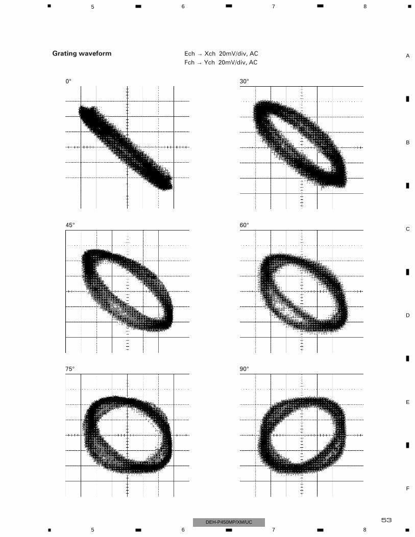
• Checking Procedure1. In test mode, load the disc and switch the 3V regulator on.2. Using the → and ← buttons, move the PU unit to the innermost track.3. Press key 3 to close focus, the display should read "91". Press key 2 to implement the tracking balance adjustment the display should now read "81". Press key 3. The display will change, returning to "81" on the fourth press.4. As shown in the diagram above, monitor the LPF outputs using the oscilloscope and check that the phase difference is within 75° . Refer to the photographs supplied to determine the phase angle.5. If the phase difference is determined to be greater than 75° try changing the PU unit to see if there is any improvement. If, after trying this a number of times, the grating angle does not become less than 75° then the mechanism should be judged to be at fault.• NoteBecause of eccentricity in the disc and a slight misalignment of the clamping center the grating waveform may be seen to "wobble" ( the phase difference changes as the disc rotates). The angle specified above indicates the average angle.
• HintReloading the disc changes the clamp position and may decrease the "wobble".
100kΩ
390pF
100kΩ
390pF
E
VREF
F
VREF
Xch Ych
L.P.F.
L.P.F.
REFO1
F E
CD CORE UNIT(S10MP3)
Oscilloscope
6.3 CHECKING THE GRATING AFTER CHANGING THE PICKUP UNIT
53
5 6 7 8
F
E
D
C
B
A
5 6 7 8DEH-P450MP/XM/UC
Grating waveform
45°
0°
75°
60°
30°
90°
Ech → Xch 20mV/div, ACFch → Ych 20mV/div, AC
54
1 2 3 4
1 2 3 4
F
E
D
C
B
A
DEH-P450MP/XM/UC
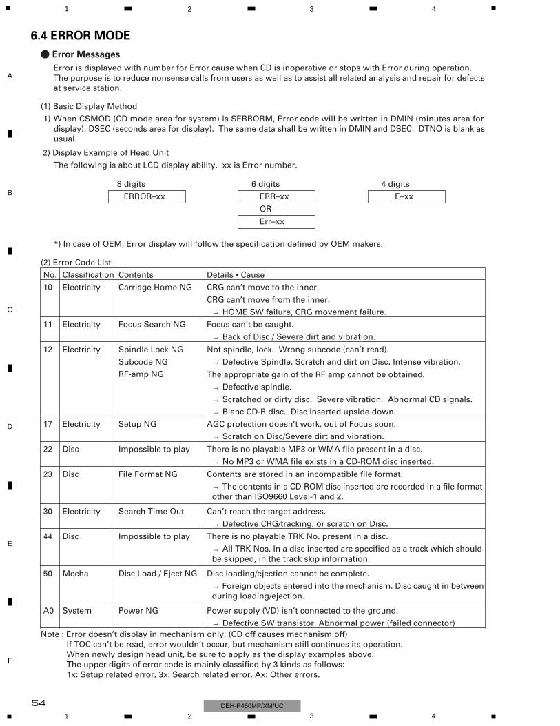
- Error Messages
Error is displayed with number for Error cause when CD is inoperative or stops with Error during operation.The purpose is to reduce nonsense calls from users as well as to assist all related analysis and repair for defects at service station.
(1) Basic Display Method
1) When CSMOD (CD mode area for system) is SERRORM, Error code will be written in DMIN (minutes area for display), DSEC (seconds area for display). The same data shall be written in DMIN and DSEC. DTNO is blank as usual.
2) Display Example of Head Unit
The following is about LCD display ability. xx is Error number.
*) In case of OEM, Error display will follow the specification defined by OEM makers.
8 digits 6 digits 4 digits
ERROR–xx ERR–xx E–xx
(2) Error Code List
No. Classification Contents Details • Cause
10 Electricity Carriage Home NG CRG can’t move to the inner.
CRG can’t move from the inner.
→ HOME SW failure, CRG movement failure.
11 Electricity Focus Search NG Focus can’t be caught.
→ Back of Disc / Severe dirt and vibration.
23 Disc File Format NG Contents are stored in an incompatible file format.
→ The contents in a CD-ROM disc inserted are recorded in a file format other than ISO9660 Level-1 and 2.
22 Disc Impossible to play There is no playable MP3 or WMA file present in a disc.
→ No MP3 or WMA file exists in a CD-ROM disc inserted.
17 Electricity Setup NG AGC protection doesn’t work, out of Focus soon.
→ Scratch on Disc/Severe dirt and vibration.
12 Electricity Spindle Lock NG Not spindle, lock. Wrong subcode (can’t read).
Subcode NG
RF-amp NG
→ Defective Spindle. Scratch and dirt on Disc. Intense vibration.
The appropriate gain of the RF amp cannot be obtained.
→ Defective spindle.
→ Blanc CD-R disc. Disc inserted upside down.
→ Scratched or dirty disc. Severe vibration. Abnormal CD signals.
30 Electricity Search Time Out Can’t reach the target address.
→ Defective CRG/tracking, or scratch on Disc.
→ All TRK Nos. In a disc inserted are specified as a track which should be skipped, in the track skip information.
44 Disc Impossible to play There is no playable TRK No. present in a disc.
50 Mecha Disc Load / Eject NG Disc loading/ejection cannot be complete.
→ Foreign objects entered into the mechanism. Disc caught in between during loading/ejection.
A0 System Power NG Power supply (VD) isn’t connected to the ground.
→ Defective SW transistor. Abnormal power (failed connector)
OR
Err–xx
Note : Error doesn’t display in mechanism only. (CD off causes mechanism off) If TOC can’t be read, error wouldn’t occur, but mechanism still continues its operation. When newly design head unit, be sure to apply as the display examples above. The upper digits of error code is mainly classified by 3 kinds as follows: 1x: Setup related error, 3x: Search related error, Ax: Other errors.
6.4 ERROR MODE
55
5 6 7 8
F
E
D
C
B
A
5 6 7 8DEH-P450MP/XM/UC
1
1
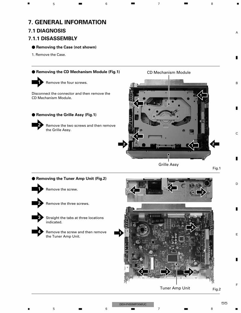
Fig.1
Fig.2
- Removing the CD Mechanism Module (Fig.1)
- Removing the Tuner Amp Unit (Fig.2)
Remove the four screws.
Remove the screw.
1. Remove the Case.
- Removing the Case (not shown)
Disconnect the connector and then remove theCD Mechanism Module.
- Removing the Grille Assy (Fig.1)
2 Remove the two screws and then removethe Grille Assy.
1
1
2 2
CD Mechanism Module
Grille Assy
1
22
2
3 3 3
4
Tuner Amp Unit
2 Remove the three screws.
3 Straight the tabs at three locations indicated.
4 Remove the screw and then remove the Tuner Amp Unit.
1
1
7. GENERAL INFORMATION
7.1 DIAGNOSIS
7.1.1 DISASSEMBLY

56
1 2 3 4
1 2 3 4
F
E
D
C
B
A
DEH-P450MP/XM/UC
- Removing the Pickup Unit1. Set the mechanism to the clamp mode.2. Remove the lead wires from the inner holder.3. Remove the two washers, styling holder, change arm, and pickup lock arm.4. While releasing from the hook of the inner holder, lift the end of the feed screw.Caution: In assembling, move the planet gear to the load/eject position before setting the feed screw in the inner holder.
Planet Gear
Change Arm
Inner Holder
Styling Holder
Feed Screw
Washer
Pickup Lock Arm
- How to hold the Mechanism Unit1. Hold the top and bottom frame.2. Do not squeeze top frame's front portion too tight, because it is fragile.
- Removing the Upper and Lower Frames1. With a disc clamped, remove the four springs (A), the two springs (B), the two springs (C), and the four screws.2. To remove the upper frame, open it on the fulcrum A.3. While lifting the carriage mechanism, remove the three dampers.4. With the frames removed, insert the connectors coming from the main unit and eject the disc.Caution: Before installing the carriage mechanism in the frames, be sure to apply some alcohol to the dampers and set the mechanism to the clamp mode.
Do not squeeze.
Lower FrameDamper
Carriage Mechanism
A
C
A
B
B
Damper
Damper
C
A
A
A
Upper Frame
57
5 6 7 8
F
E
D
C
B
A
5 6 7 8DEH-P450MP/XM/UC
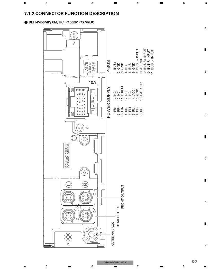
10A2
164
68
1012
141
153
57
911
13
1. F
R+
2. R
R+
3. F
R-
4. R
R-
5. F
L+6.
RL+
7. F
L-8.
RL-
9. N
C10
. NC
11. B
.RE
M12
. NC
13. N
C14
. AC
C15
. GN
D16
. BA
CK
UP
1. B
US
+ 2
. GN
D 3
. GN
D 4
. NC
5. B
US
- 6
. GN
D 7
. BU
S L
+ IN
PU
T 8
. AS
EN
B 9
. BU
S R
+ IN
PU
T10
. BU
S R
- IN
PU
T11
. BU
S L
- IN
PU
T
1110
98
76
5
43
21
PO
WE
R S
UP
PLY
IP-B
US
AN
TE
NN
A J
AC
K
RE
AR
OU
TP
UT FR
ON
T O
UT
PU
T
7.1.2 CONNECTOR FUNCTION DESCRIPTION
- DEH-P450MP/XM/UC, P4500MP/XM/UC
58
1 2 3 4
1 2 3 4
F
E
D
C
B
A
DEH-P450MP/XM/UC
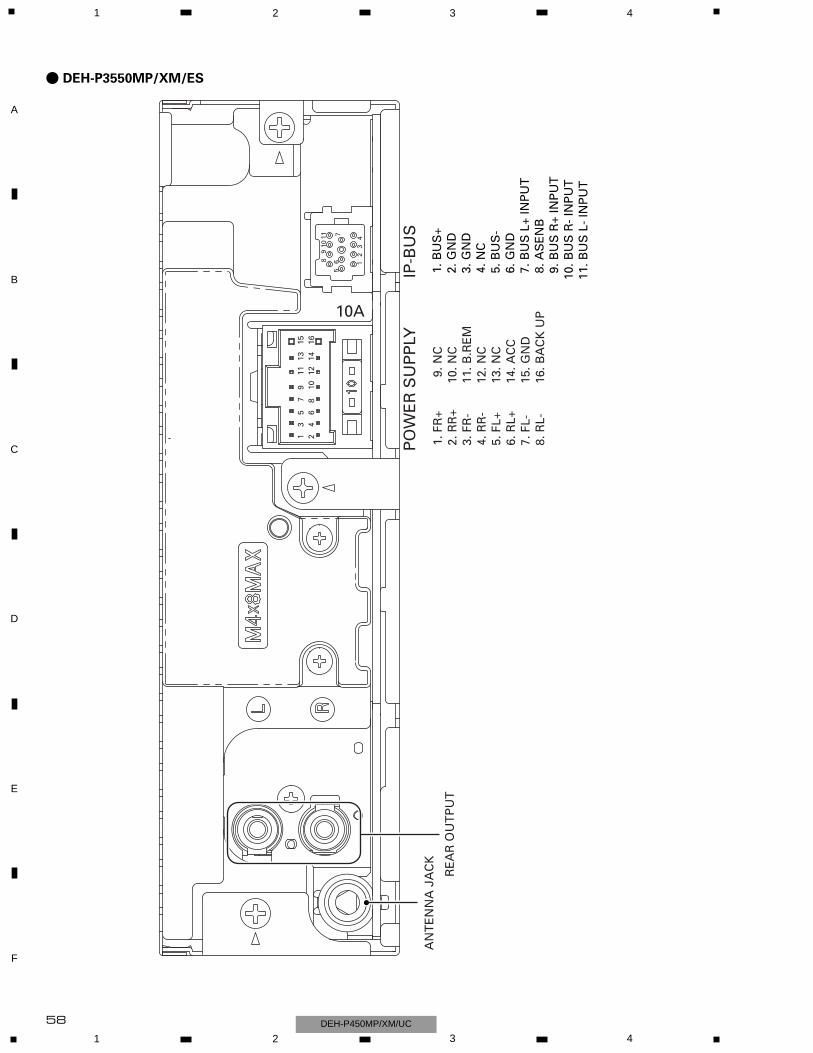
10A2
164
68
1012
141
153
57
911
13
1. F
R+
2. R
R+
3. F
R-
4. R
R-
5. F
L+6.
RL+
7. F
L-8.
RL-
9. N
C10
. NC
11. B
.RE
M12
. NC
13. N
C14
. AC
C15
. GN
D16
. BA
CK
UP
AN
TE
NN
A J
AC
K
RE
AR
OU
TP
UT
1. B
US
+ 2
. GN
D 3
. GN
D 4
. NC
5. B
US
- 6
. GN
D 7
. BU
S L
+ IN
PU
T 8
. AS
EN
B 9
. BU
S R
+ IN
PU
T10
. BU
S R
- IN
PU
T11
. BU
S L
- IN
PU
T
1110
98
76
5
43
21
PO
WE
R S
UP
PLY
IP-B
US
- DEH-P3550MP/XM/ES
59
5 6 7 8
F
E
D
C
B
A
5 6 7 8DEH-P450MP/XM/UC
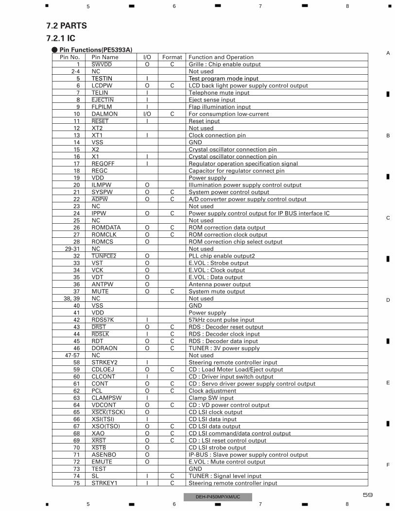
- Pin Functions(PE5393A)Pin No. Pin Name I/O Format Function and Operation
1 swvdd O C Grille : Chip enable output2-4 NC Not used
5 TESTIN I Test program mode input6 LCDPW O C LCD back light power supply control output7 TELIN I Telephone mute input8 ejectin I Eject sense input9 FLPILM I Flap illumination input
10 DALMON I/O C For consumption low-current11 reset I Reset input12 XT2 Not used13 XT1 I Clock connection pin14 VSS GND15 X2 Crystal oscillator connection pin16 X1 I Crystal oscillator connection pin17 REGOFF I Regulator operation specification signal18 REGC Capacitor for regulator connect pin19 VDD Power supply20 ILMPW O Illumination power supply control output21 SYSPW O C System power control output22 adpw O C A/D converter power supply control output23 NC Not used24 IPPW O C Power supply control output for IP BUS interface IC25 NC Not used26 ROMDATA O C ROM correction data output27 ROMCLK O C ROM correction clock output28 ROMCS O ROM correction chip select output
29-31 NC Not used32 tunpce@ O PLL chip enable output233 VST O E.VOL : Strobe output34 VCK O E.VOL : Clock output35 VDT O E.VOL : Data output36 ANTPW O Antenna power output37 MUTE O C System mute output
38, 39 NC Not used40 VSS GND41 VDD Power supply42 RDS57K I 57kHz count pulse input43 drst O C RDS : Decoder reset output44 rdslk I C RDS : Decoder clock input45 RDT O C RDS : Decoder data input46 DORAON O C TUNER : 3V power supply
47-57 NC Not used58 STRKEY2 I Steering remote controller input59 CDLOEJ O C CD : Load Moter Load/Eject output60 CLCONT I CD : Driver input switch output61 CONT O C CD : Servo driver power supply control output62 PCL O C Clock adjustment63 CLAMPSW I Clamp SW input64 VDCONT O C CD : VD power control output65 xsck(TSCK) O CD LSI clock output66 XSI(TSI) I CD LSI data input67 XSO(TSO) O C CD LSI data output68 XAO O C CD LSI command/data control output69 xrst O C CD : LSI reset control output70 xstb O CD LSI strobe output71 ASENBO O IP-BUS : Slave power supply control output72 EMUTE O E.VOL : Mute control output73 TEST GND74 SL I C TUNER : Signal level input75 STRKEY1 I C Steering remote controller input
7.2 PARTS
7.2.1 IC

60
1 2 3 4
1 2 3 4
F
E
D
C
B
A
DEH-P450MP/XM/UC
Pin No. Pin Name I/O Format Function and Operation76 MODELIN I Model select input77 CSENS I Flap close sense input78 NC Not used79 DSCSNS I CD : Disc insert sense input80 VDSENS I CD : VD voltage sense input 81 TEMP I CD : Temperature sense input82 AVDD A/D converter power supply terminal83 AVREF A/D converter reference voltage terminal84 AVSS GND85 RX I IP-BUS : Data input86 TX O IP-BUS : Data output87 NMI GND88 ldet I PLL lock sense input89 rck I RDS : Clock input90 dsens I Grille detach sense input91 PACK I PACK input92 asens I ACC power sense input93 bsens I Back up power sense input94 TUNPDI I PLL IC data input95 KYDT I Grille data input96 DPDT O C Grille data output97 TUNPCK O PLL clock output98 TUNPDO O C PLL data output99 TUNPCE O C PLL chip enable output
100 PEE O C Beep tone output
* PE5393A
30
3150
51
80
81 100
1
Format Meaning
C CMOS
IC's marked by * are MOS type.Be careful in handling them because they are very liable to be damaged by electrostatic induction.
1 2 3
VD
D
GN
D
5 4
VO
UT
N.C
.
N.C
.
Vref
BD4834G
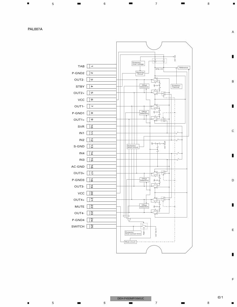
61
5 6 7 8
F
E
D
C
B
A
5 6 7 8DEH-P450MP/XM/UC
1
TAB
2
P-GND2
3
OUT2-
4
STBY
5
OUT2+
6
VCC
7
OUT1-
8
P-GND1
9
OUT1+
10SVR
11IN1
12IN2
13S-GND
14IN4
15IN3
16AC-GND
17OUT3+
18P-GND3
19OUT3-
20VCC
21OUT4+
22MUTE
23OUT4-
24P-GND4
SWITCH
25
+-
+ -
OffsetDetection
+-
+ -
OffsetDetection
+-
+ -
OffsetDetection
+-
+ -
OffsetDetection
Protector;Over current limit
sw_v
cc
stby
Protector;Short circuit
Mute circuit
am
p_v
ccStand-by
Circuit
Protector;Over voltage
sw_v
cc
Protector;Thermal
Referenceamp_vcc
PAL007A
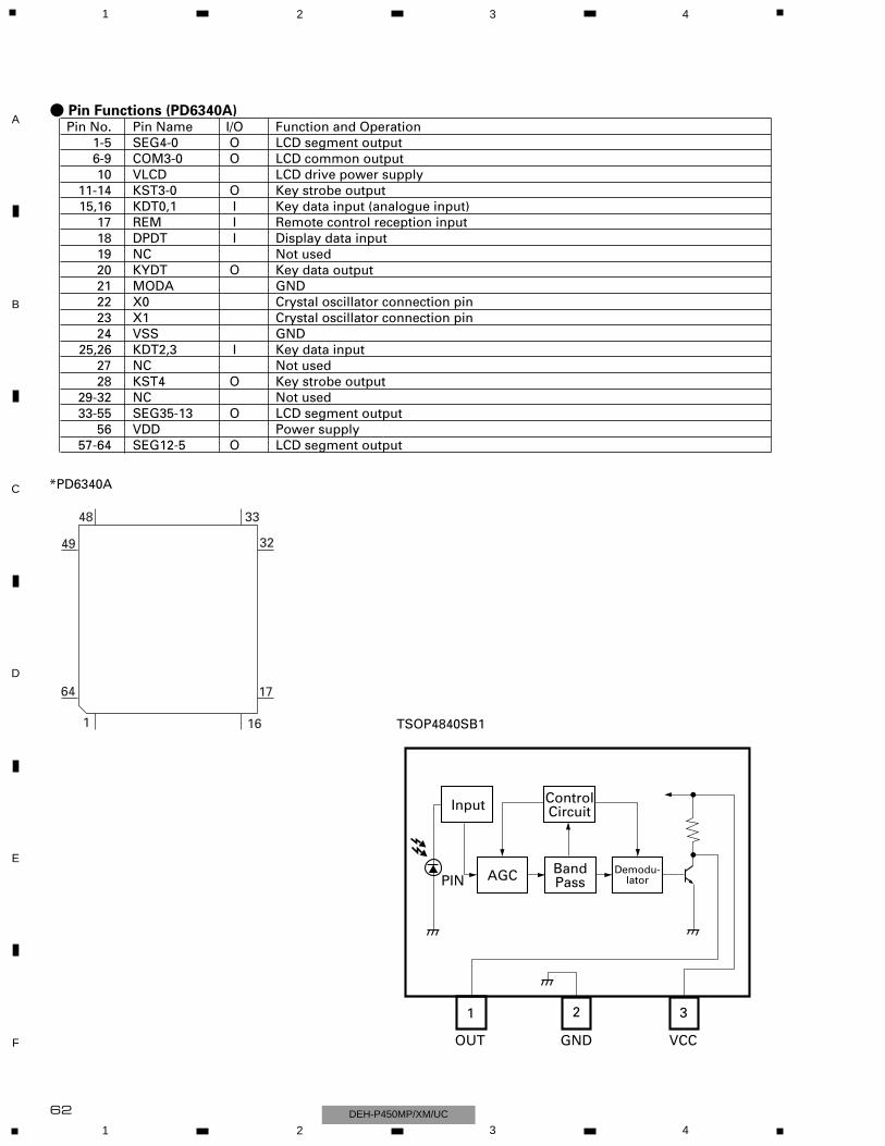
62
1 2 3 4
1 2 3 4
F
E
D
C
B
A
DEH-P450MP/XM/UC
TSOP4840SB1
- Pin Functions (PD6340A)Pin No. Pin Name I/O Function and Operation
1-5 SEG4-0 O LCD segment output6-9 COM3-0 O LCD common output 10 VLCD LCD drive power supply
11-14 KST3-0 O Key strobe output15,16 KDT0,1 I Key data input (analogue input)
17 REM I Remote control reception input18 DPDT I Display data input19 NC Not used20 KYDT O Key data output21 MODA GND22 X0 Crystal oscillator connection pin23 X1 Crystal oscillator connection pin24 VSS GND
25,26 KDT2,3 I Key data input27 NC Not used28 KST4 O Key strobe output
29-32 NC Not used33-55 SEG35-13 O LCD segment output
56 VDD Power supply57-64 SEG12-5 O LCD segment output
*PD6340A
16
17
32
3348
49
64
1
OUT GND VCC
PIN
1 2 3
ControlCircuit
BandPassAGC
Input
Demodu-lator
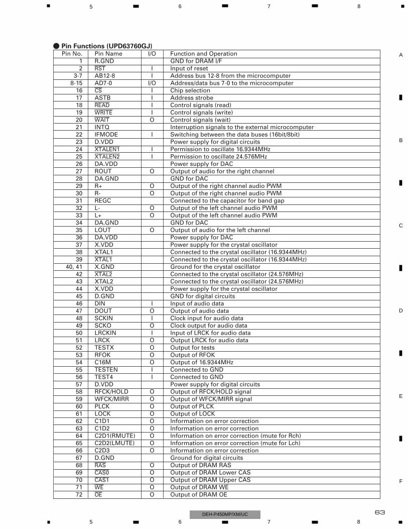
63
5 6 7 8
F
E
D
C
B
A
5 6 7 8DEH-P450MP/XM/UC
- Pin Functions (UPD63760GJ)Pin No. Pin Name I/O Function and Operation
1 R.GND GND for DRAM I/F2 rst I Input of reset
3-7 AB12-8 I Address bus 12-8 from the microcomputer8-15 AD7-0 I/O Address/data bus 7-0 to the microcomputer
16 cs I Chip selection17 ASTB I Address strobe18 read I Control signals (read)19 write I Control signals (write)20 wait O Control signals (wait)21 INTQ Interruption signals to the external microcomputer22 IFMODE I Switching between the data buses (16bit/8bit)23 D.VDD Power supply for digital circuits24 xtalen! I Permission to oscillate 16.9344MHz25 xtalen@ I Permission to oscillate 24.576MHz26 DA.VDD Power supply for DAC27 ROUT O Output of audio for the right channel28 DA.GND GND for DAC29 R+ O Output of the right channel audio PWM30 R- O Output of the right channel audio PWM31 REGC Connected to the capacitor for band gap32 L- O Output of the left channel audio PWM33 L+ O Output of the left channel audio PWM34 DA.GND GND for DAC35 LOUT O Output of audio for the left channel36 DA.VDD Power supply for DAC37 X.VDD Power supply for the crystal oscillator38 XTAL1 Connected to the crystal oscillator (16.9344MHz)39 xtal! Connected to the crystal oscillator (16.9344MHz)
40, 41 X.GND Ground for the crystal oscillator42 xtal@ Connected to the crystal oscillator (24.576MHz)43 XTAL2 Connected to the crystal oscillator (24.576MHz)44 X.VDD Power supply for the crystal oscillator45 D.GND GND for digital circuits46 DIN I Input of audio data47 DOUT O Output of audio data48 SCKIN I Clock input for audio data49 SCKO O Clock output for audio data50 LRCKIN I Input of LRCK for audio data51 LRCK O Output LRCK for audio data52 TESTX O Output for tests53 RFOK O Output of RFOK54 C16M O Output of 16.9344MHz55 TESTEN I Connected to GND56 TEST4 I Connected to GND57 D.VDD Power supply for digital circuits58 RFCK/HOLD O Output of RFCK/HOLD signal59 WFCK/MIRR O Output of WFCK/MIRR signal60 PLCK O Output of PLCK61 LOCK O Output of LOCK62 C1D1 O Information on error correction63 C1D2 O Information on error correction64 C2D1(RMUTE) O Information on error correction (mute for Rch)65 C2D2(LMUTE) O Information on error correction (mute for Lch)66 C2D3 O Information on error correction 67 D.GND Ground for digital circuits68 ras O Output of DRAM RAS69 cas) O Output of DRAM Lower CAS70 cas! O Output of DRAM Upper CAS71 we O Output of DRAM WE72 oe O Output of DRAM OE
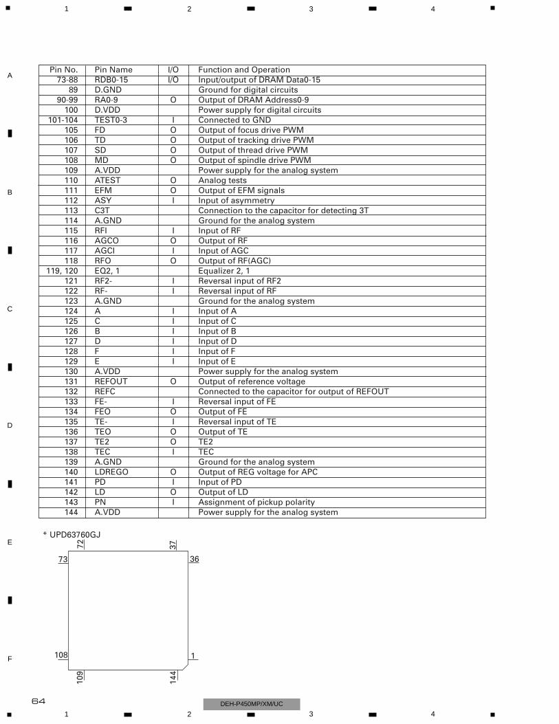
64
1 2 3 4
1 2 3 4
F
E
D
C
B
A
DEH-P450MP/XM/UC
Pin No. Pin Name I/O Function and Operation73-88 RDB0-15 I/O Input/output of DRAM Data0-15
89 D.GND Ground for digital circuits90-99 RA0-9 O Output of DRAM Address0-9
100 D.VDD Power supply for digital circuits101-104 TEST0-3 I Connected to GND
105 FD O Output of focus drive PWM106 TD O Output of tracking drive PWM107 SD O Output of thread drive PWM108 MD O Output of spindle drive PWM109 A.VDD Power supply for the analog system110 ATEST O Analog tests111 EFM O Output of EFM signals112 ASY I Input of asymmetry113 C3T Connection to the capacitor for detecting 3T114 A.GND Ground for the analog system115 RFI I Input of RF116 AGCO O Output of RF117 AGCI I Input of AGC118 RFO O Output of RF(AGC)
119, 120 EQ2, 1 Equalizer 2, 1121 RF2- I Reversal input of RF2122 RF- I Reversal input of RF123 A.GND Ground for the analog system124 A I Input of A125 C I Input of C126 B I Input of B127 D I Input of D128 F I Input of F129 E I Input of E130 A.VDD Power supply for the analog system131 REFOUT O Output of reference voltage132 REFC Connected to the capacitor for output of REFOUT133 FE- I Reversal input of FE134 FEO O Output of FE135 TE- I Reversal input of TE136 TEO O Output of TE137 TE2 O TE2138 TEC I TEC139 A.GND Ground for the analog system140 LDREGO O Output of REG voltage for APC141 PD I Input of PD142 LD O Output of LD143 PN I Assignment of pickup polarity144 A.VDD Power supply for the analog system
* UPD63760GJ
36
3772
73
144
1
109
108

65
5 6 7 8
F
E
D
C
B
A
5 6 7 8DEH-P450MP/XM/UC
- Pin Functions (PE5352B)Pin No. Pin Name I/O Format Function and Operation
1 BSO O C P-Bus serial data output2 bsck I/O /C P-Bus serial clock input/output
3, 4 DFS1, 2 O C DA I/F IC sampling frequency setting output 1, 25 DCKS O C DA I/F IC clock subharmonic number selection output6 EVDD E power supply Positive power supply7 EVSS E power supply GND8 dspok I DSP microcomputer initialization OK input9 DCOPY O C DA I/F IC copy flag setting output
10 crst O C Compression IC reset control output11, 12 NC Not used
13 EMPH O C Emphasis information output14 emph O C Emphasis information output15 DSPMUTE O C DOUT mute output16 DSET O C Disc set indicator lighting output17 adena O C A/D reference voltage supply control output18 IC/VPP IC : VSS direct connection/VPP : Pull-down19 BRXEN I/O /C P-Bus reception is possible20 bsrq I/O /C P-Bus service request demand21 xtalen! O C CD LSI 16.9344MHz oscillation permission output22 xtalen@ O C CD LSI 24.576MHz oscillation permission output23 xrst O C CD LSI reset control output24 VDCONT O C VD power supply control output25 CD3VON O C CD +3.3V power supply control output26 CONT O C Servo driver power supply control output27 xwait I CD LSI wait control signal input28 LOEJ O C The direction change output of LOAD/EJECT29 CLCONT O C Driver input change output30 CDMUTE O C CD mute control output31 reset I System reset input32 XT1 I Connected to the oscillator for subclock
(connected to VSS via the resistor)33 XT2 Connected to the oscillator for subclock (Open)34 REGC Connected to the capacity stabilizing output of the regulator
(an electrolytic capacitor of about 1µF)35 X2 Oscillator connection for mainclock36 X1 I Oscillator connection for mainclock37 VSS GND38 VDD Positive power supply (5V)39 CLKOUT O C Internal system clock output (Open)40 xwrite O CD LSI write control signal output41 uben O Not used (Open)42 WR/W O WMA decoder Read/Write control signal output43 xread O CD LSI read control signal output44 XASTB O CD LSI address strobe output45 LOCK I Spindle lock input46 wrst O C WMA decoder reset control output
47-54 AD0-7 I/O /C Address/Data bus 0-755 BVDD B power supply Positive power supply (3.3V)56 BVSS B power supply GND
57-64 AD8-15 I/O /C Address/Data bus 8-1565 xcs O C CD LSI chip selection output66 wcs O C WMA decoder chip selection output
67, 68 DBBWRDY0, 1 I Input of write-ready flag with WMA decoder DBBI0, 169, 70 DBBRRDY0, 1 I Input of read-ready flag with WMA decoder DBBO0, 1
71 AVDD A power supply Positive power supply (5V)72 AVSS A power supply GND73 AVREF The reference voltage input for A/D converter74 VDSENS VD power supply short sense input75 DSCSNS Disc state sense input76 TEMP Temperature information sense input

66
1 2 3 4
1 2 3 4
F
E
D
C
B
A
DEH-P450MP/XM/UC
Pin No. Pin Name I/O Format Function and Operation77 HOME I Home SW sense input78 csens I Flap closing sense input79 RFOKIN I RFOK input chatter count input
80-82 NC Connected to AVDD or AVSS via the resistor83 WMAARI I Input of sensing existence of WMA decoder and DA I/F IC84 TYPE_A/D I CD-DA Analog/Digital output change setup85 testin I Chip check test program starting input86 NC Connected to EVDD or EVSS via the resistor87 xint CD LSI interruption signal input88 wint WMA decoder interruption signal input89 brst I P-Bus reset input90 ejsw I Eject key input
91, 92 NC Open93 CLAMP I C CLAMP SW sense input94 ROMDATA I/O /C E2PROM data input/output95 ROMCS O C E2PROM chip selection output96 ROMCK O C E2PROM clock output97 FRXD I For flash rewriting (received signal)98 FTXD O C For flash rewriting (transmitted signal)99 AO/DO O C The output for Analog/Digital voice output distinction
100 BSI I P-Bus serial data input
* PE5352B
25
2650
51
75
76 100
1
Format Meaning
C CMOS
DQ
12
DQ
23
DQ
34
DQ
45
VC
C6
DQ
57
DQ
68
DQ
79
DQ
810
NC
13
NC
14
we
15
ra
s16
NC
17
A0
18
A1
19
A2
20
A3
21
VC
C22
42D
Q15
41D
Q14
40D
Q13
39V
SS
38D
Q12
37D
Q11
36D
Q10
35D
Q9
32N
C
31lc
as
30h
ca
s
29o
e
28A
8
27A
7
26A
6
25A
5
24A
4
23V
SS
VC
C1
43D
Q16
44V
SS
A0-
A8
:Ad
dre
ss in
pu
tr
as
: R
ow
ad
dre
ss s
tro
be
lca
s :
Low
er c
olu
mn
ad
dre
ss s
tro
be
uc
as
: U
pp
er c
olu
mn
ad
dre
ss s
tro
be
DQ
1-D
Q16
: D
ata
inp
ut/
dat
a o
utp
ut
oe :
Ou
tpu
t en
able
w
e :
Wri
te e
nab
le
VC
C :
Po
wer
su
pp
lyV
SS
: G
ND
NC
: N
o c
on
nec
tio
n
MSM51V4265EP-70TS
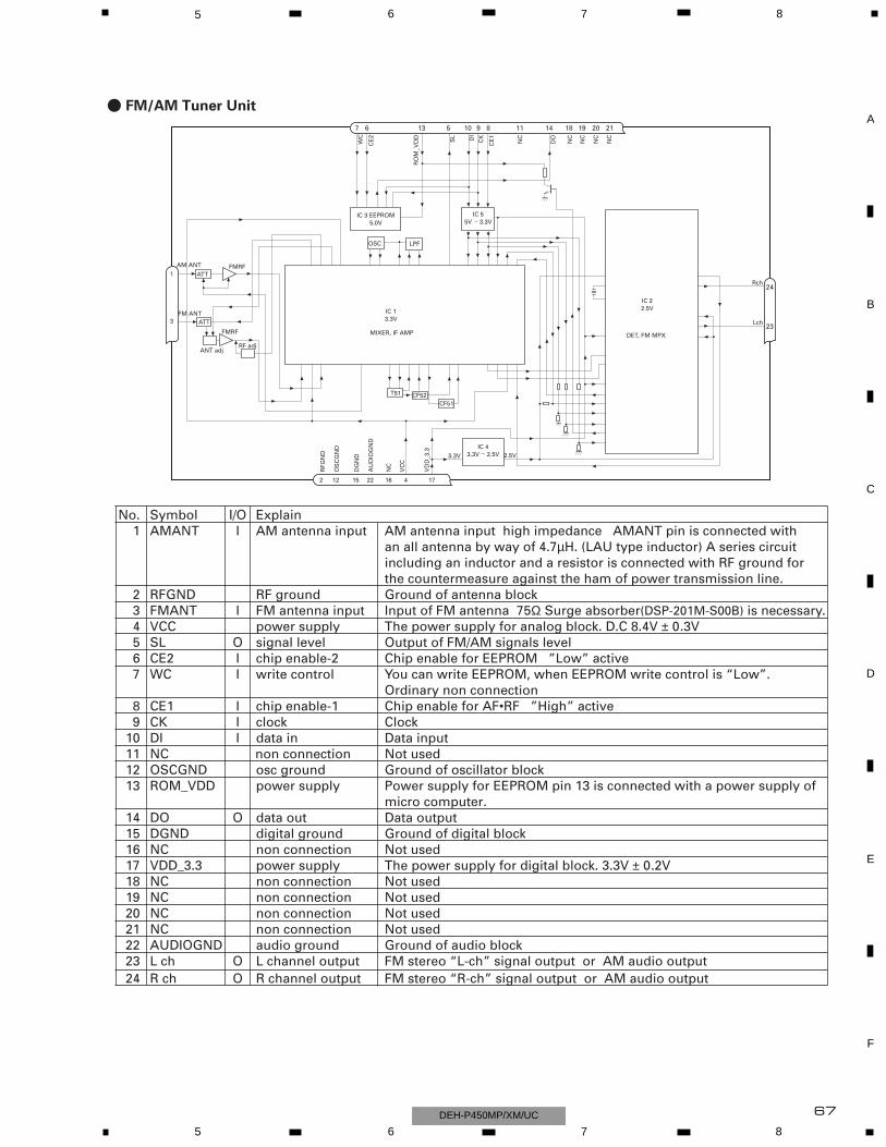
67
5 6 7 8
F
E
D
C
B
A
5 6 7 8DEH-P450MP/XM/UC
No. Symbol I/O Explain1 AMANT I AM antenna input AM antenna input high impedance AMANT pin is connected with
an all antenna by way of 4.7µH. (LAU type inductor) A series circuit including an inductor and a resistor is connected with RF ground for the countermeasure against the ham of power transmission line.
2 RFGND RF ground Ground of antenna block3 FMANT I FM antenna input Input of FM antenna 75Ω Surge absorber(DSP-201M-S00B) is necessary.4 VCC power supply The power supply for analog block. D.C 8.4V ± 0.3V5 SL O signal level Output of FM/AM signals level6 CE2 I chip enable-2 Chip enable for EEPROM ”Low” active7 WC I write control You can write EEPROM, when EEPROM write control is “Low”.
Ordinary non connection8 CE1 I chip enable-1 Chip enable for AF•RF ”High” active9 CK I clock Clock
10 DI I data in Data input11 NC non connection Not used12 OSCGND osc ground Ground of oscillator block13 ROM_VDD power supply Power supply for EEPROM pin 13 is connected with a power supply of
micro computer.14 DO O data out Data output15 DGND digital ground Ground of digital block16 NC non connection Not used17 VDD_3.3 power supply The power supply for digital block. 3.3V ± 0.2V18 NC non connection Not used19 NC non connection Not used20 NC non connection Not used21 NC non connection Not used22 AUDIOGND audio ground Ground of audio block23 L ch O L channel output FM stereo “L-ch” signal output or AM audio output 24 R ch O R channel output FM stereo “R-ch” signal output or AM audio output
FMRF
ANT adjRF adj
FM ANT
T51 CF52CF51
RFG
ND
OS
CG
ND
DG
ND
AU
DIO
GN
D
NC
VC
C
VD
D_3
.3
3.3V 2.5VIC 4
3.3V 2.5V
←
IC 22.5V
WC
CE
2
RO
M_V
DD SL DI
CK
CE
1
NC
DO
NC
NC
NC
NC
7 6 13 5 10 9 8 11 14 18 19 20 21
1
3
2 12 15 22 16 4 17
IC 13.3V
AM ANT FMRFATT
LPFOSC
IC 3 EEPROM5.0V
IC 55V 3.3V←
ATT
MIXER, IF AMP DET, FM MPX
24
23
Rch
Lch
- FM/AM Tuner Unit
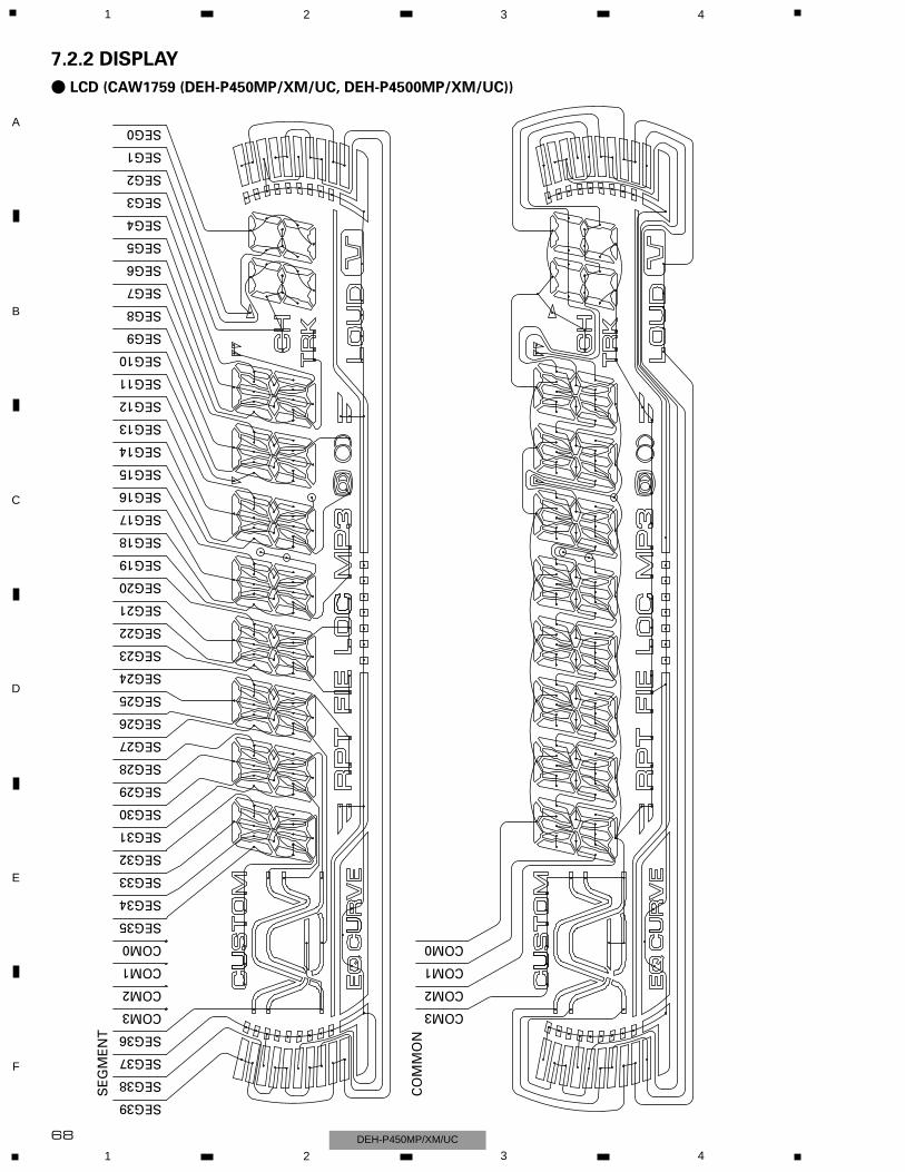
68
1 2 3 4
1 2 3 4
F
E
D
C
B
A
DEH-P450MP/XM/UC
SEG39
SEG38
SEG37
SEG36
COM3
COM2
COM1
COM0
SEG35
SEG34
SEG33
SEG32
SEG31
SEG30
SEG29
SEG28
SEG27
SEG26
SEG25
SEG24
SEG23
SEG22
SEG21
SEG20
SEG19
SEG18
SEG17
SEG16
SEG15
SEG14
SEG13
SEG12
SEG11
SEG10
SEG9
SEG8
SEG7
SEG6
SEG5
SEG4
SEG3
SEG2
SEG1
SEG0
COM3
CO
MM
ON
SE
GM
EN
T
COM2
COM1
COM0
7.2.2 DISPLAY
- LCD (CAW1759 (DEH-P450MP/XM/UC, DEH-P4500MP/XM/UC))
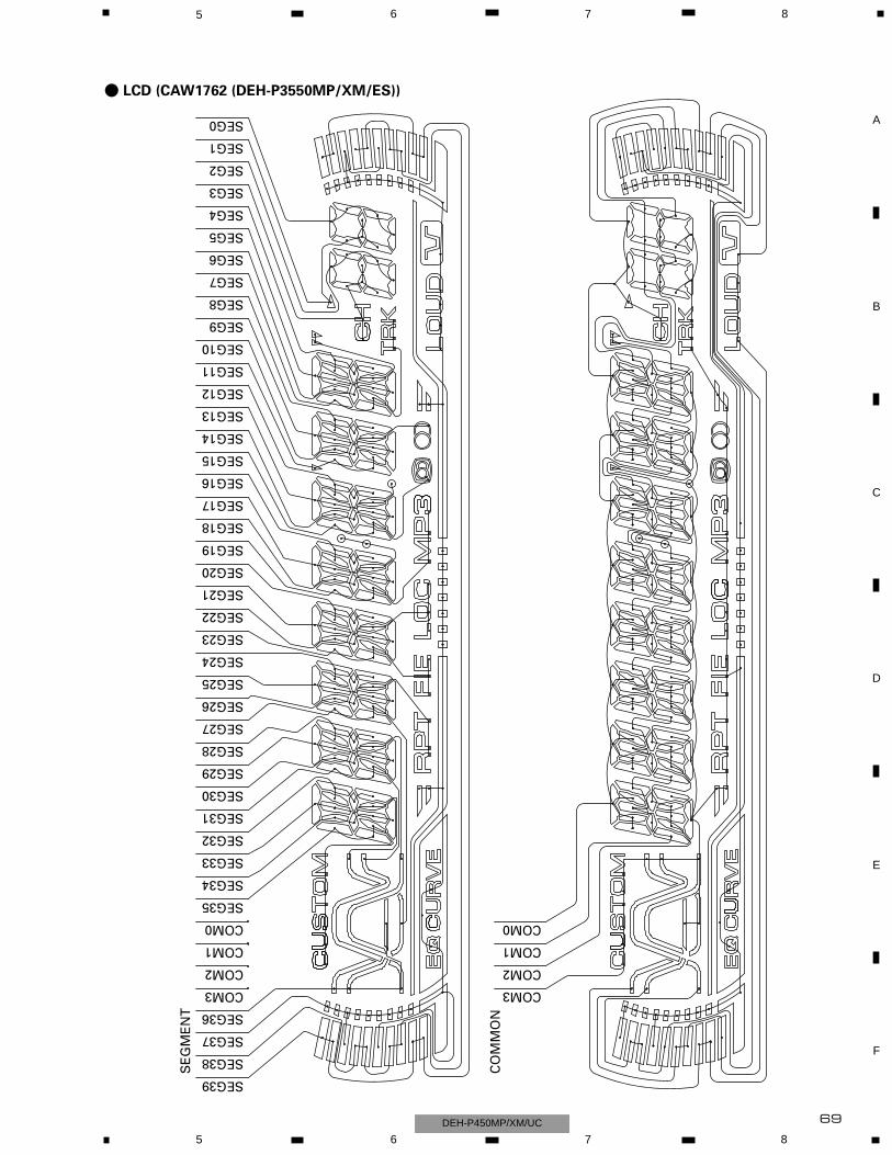
69
5 6 7 8
F
E
D
C
B
A
5 6 7 8DEH-P450MP/XM/UC
SEG39
SEG38
SEG37
SEG36
COM3
COM2
COM1
COM0
SEG35
SEG34
SEG33
SEG32
SEG31
SEG30
SEG29
SEG28
SEG27
SEG26
SEG25
SEG24
SEG23
SEG22
SEG21
SEG20
SEG19
SEG18
SEG17
SEG16
SEG15
SEG14
SEG13
SEG12
SEG11
SEG10
SEG9
SEG8
SEG7
SEG6
SEG5
SEG4
SEG3
SEG2
SEG1
SEG0
COM3
CO
MM
ON
SE
GM
EN
TCOM2
COM1
COM0
- LCD (CAW1762 (DEH-P3550MP/XM/ES))
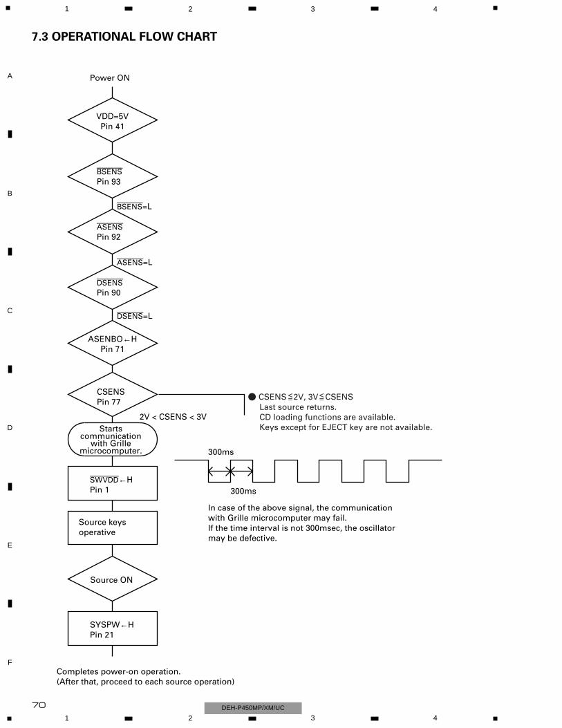
70
1 2 3 4
1 2 3 4
F
E
D
C
B
A
DEH-P450MP/XM/UC
VDD=5VPin 41
ASENBO←HPin 71
Power ON
bsens=L
asens=L
dsens=L
bsensPin 93
asensPin 92
dsensPin 90
swvdd←HPin 1
Source keys operative
Completes power-on operation.(After that, proceed to each source operation)
SYSPW←HPin 21
Startscommunication
with Grillemicrocomputer.
Source ON
300ms
300ms
In case of the above signal, the communication with Grille microcomputer may fail.If the time interval is not 300msec, the oscillator may be defective.
CSENSPin 77
2V < CSENS < 3V
- CSENS 2V, 3V CSENS Last source returns. CD loading functions are available. Keys except for EJECT key are not available.
< <= =
7.3 OPERATIONAL FLOW CHART
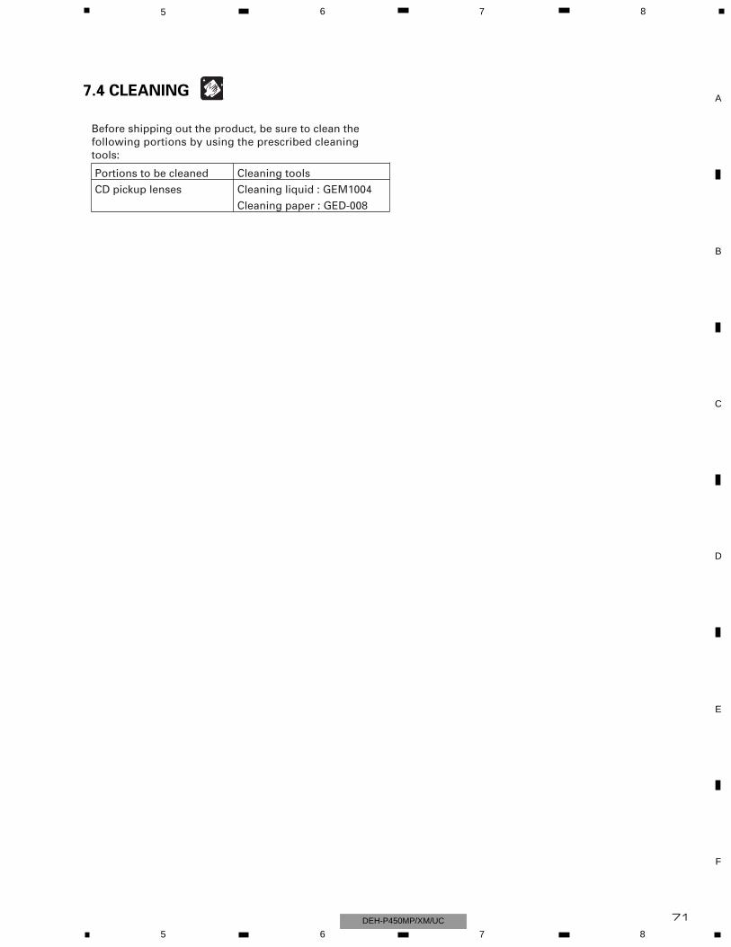
71
5 6 7 8
F
E
D
C
B
A
5 6 7 8DEH-P450MP/XM/UC
Before shipping out the product, be sure to clean the following portions by using the prescribed cleaning tools:
Portions to be cleaned Cleaning tools
CD pickup lenses Cleaning liquid : GEM1004
Cleaning paper : GED-008
7.4 CLEANING
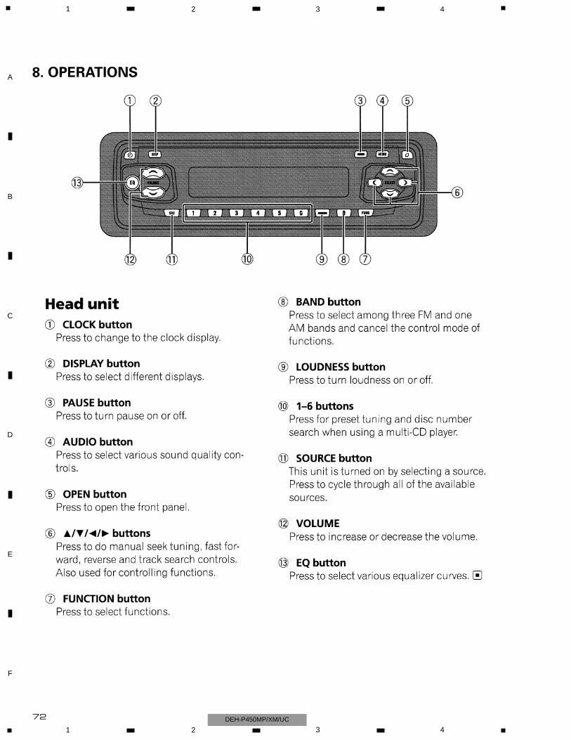
72
1 2 3 4
1 2 3 4
F
E
D
C
B
A
DEH-P450MP/XM/UC
8. OPERATIONS

73
5 6 7 8
F
E
D
C
B
A
5 6 7 8DEH-P450MP/XM/UC
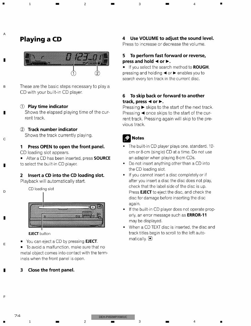
74
1 2 3 4
1 2 3 4
F
E
D
C
B
A
DEH-P450MP/XM/UC
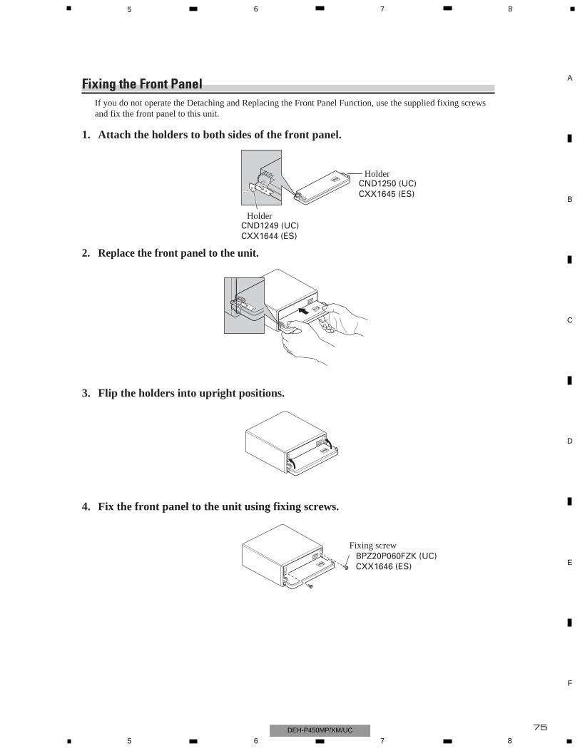
75
5 6 7 8
F
E
D
C
B
A
5 6 7 8DEH-P450MP/XM/UC
Fixing the Front PanelIf you do not operate the Detaching and Replacing the Front Panel Function, use the supplied fixing screwsand fix the front panel to this unit.
1. Attach the holders to both sides of the front panel.
2. Replace the front panel to the unit.
3. Flip the holders into upright positions.
4. Fix the front panel to the unit using fixing screws.
Fixing screw
HolderCND1249 (UC)CXX1644 (ES)
HolderCND1250 (UC)CXX1645 (ES)
BPZ20P060FZK (UC)CXX1646 (ES)
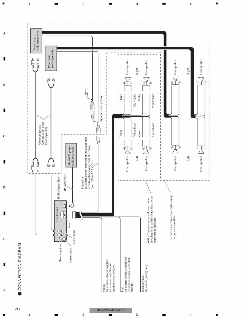
76
1 2 3 4
1 2 3 4
F
E
D
C
B
A
DEH-P450MP/XM/UC
- C
ON
NE
CT
ION
DIA
GR
AM
+ ≠
+ ≠
+ ≠
+ ≠
IP-B
US
inpu
t(B
lue)
Thi
sPr
oduc
t
Blu
e/w
hite
Tosy
stem
cont
rolt
erm
inal
ofth
epo
wer
amp
orA
uto-
ante
nna
rela
yco
ntro
lter
min
al(m
ax.3
00m
A12
VD
C).
Con
nect
ing
cord
sw
ithR
CA
pin
plug
s(s
old
sepa
rate
ly)
Syst
emre
mot
eco
ntro
l
Rea
rsp
eake
rR
ear
spea
ker
Rig
ht
Fron
tspe
aker
Rea
rsp
eake
r
Whi
teG
ray
Whi
te/b
lack
Gre
en
Gre
en/b
lack
Gra
y/bl
ack
Vio
let
Vio
let/b
lack
Fron
tspe
aker
Rea
rsp
eake
r
Left
With
a2
spea
ker
syst
em,d
ono
tcon
nect
anyt
hing
toth
esp
eake
rle
ads
that
are
not
conn
ecte
dto
spea
kers
.
Yel
low
Tote
rmin
alal
way
ssu
pplie
dw
ithpo
wer
rega
rdle
ssof
igni
tion
switc
hpo
sitio
n.
Bla
ck(g
roun
d)To
vehi
cle
(met
al)
body
.
Red
Toel
ectr
icte
rmin
alco
ntro
lled
byig
nitio
nsw
itch
(12
VD
C)
ON
/OFF
.
Ant
enna
jack
Rea
rou
tput
Perf
orm
thes
eco
nnec
tions
whe
nus
ing
the
optio
nala
mpl
ifie
r.
Fron
tout
put
Pow
eram
p(s
old
sepa
rate
ly)
Fron
tspe
aker
Fron
tspe
aker
Rig
ht
Left
IP-B
US
cabl
e
Mul
ti-C
Dpl
ayer
(sol
dse
para
tely
)Fu
se
+ ≠
+ ≠
+ ≠
+ ≠
Pow
eram
p(s
old
sepa
rate
ly)

![EP1054/EP1085/EP2030 SERVICE MANUAL - Diagramas …diagramasde.com/diagramas/otros2/EP1085 Field Service Manual.pdf · EP1054/EP1085/EP2030 SERVICE MANUAL [FIELD SERVICE] [FIELD SERVICE]](https://img.pdfslide.us/doc/110x75/5a7ba4107f8b9a563b8c4155/ep1054ep1085ep2030-service-manual-diagramas-field-service-manualpdfep1054ep1085ep2030.jpg)