Embed Size (px)
Citation preview
Defense Nanotechnology Research and Development Program
December 2009 Department of Defense
Director, Defense Research & Engineering
Table of Contents
Executive Summary .................................................................................... ES-1 I. Introduction ....................................................................................................... 1 II. Goals and Challenges ........................................................................................ 2 III. Plans .................................................................................................................. 4 IV. Progress ............................................................................................................. 6 A. The United States Air Force ........................................................................ 6 1. Air Force Devices and Systems ............................................................. 6 Photon-Plasmon-Electron Conversion Enables a New Class of
Imaging Cameras ................................................................................ 6 2. Air Force Nanomaterials ........................................................................ 6 Processing of Explosive Formulations With Nano-Aluminum
Powder ................................................................................................ 6 3. Air Force Manufacturing ....................................................................... 7 Uncooled IR Detector Made Possible With Controlled
Carbon Nanotube Array ..................................................................... 7 Nanoparticle Lubricant Produced by Biosynthesis ............................... 8 B. The United States Army .............................................................................. 8 1. Army Fundamental Phenomena ............................................................ 8 Photonics ............................................................................................... 8 Piezoelectric Sensing ............................................................................. 8 Enhanced Thermoelectric Properties .................................................... 9 2. Army Nanomaterials .............................................................................. 9 Improved Polymer Composite ............................................................... 9 Chemical Sensing/Decontamination ...................................................... 9 3. Army Devices and Systems ................................................................... 9 Magnetic Resonance Force Microscopy ............................................... 9 Air-Activated Heaters ............................................................................ 9 C. The United States Navy ............................................................................... 9 1. Navy Fundamental Phenomena and Processes ...................................... 9 Electronics ............................................................................................. 9 Fundamental Thermal Properties ........................................................ 11 Nanostructure-Enhanced Thermoelectric Properties ......................... 11
iii
2. Navy Nanomaterials ............................................................................ 11 Magnetics ............................................................................................. 11 Semiconductors .................................................................................... 11 3. Navy Devices and Systems .................................................................. 11 Spin-Based Devices .............................................................................. 11 Energy Storage .................................................................................... 12 4. Navy Instrumentation/Metrology/Standards ....................................... 13 Mechanical Property Variation ........................................................... 13 5. Navy Nanomanufacturing .................................................................... 13 Cost Saving .......................................................................................... 13 D. The Defense Advanced Projects Research Agency (DARPA) ................. 13 1. DARPA Fundamental Phenomena ...................................................... 13 2. DARPA Manufacturing ....................................................................... 14 E. The Defense Threat Reduction Agency (DTRA) ...................................... 15 1. DTRA Chem/Bio (CB) Defense Functional Nanostructures .............. 15 2. DTRA CB Defense Biomimetric Design Rules .................................. 15 3. DTRA CB Defense Nanoscale Platforms ............................................ 15 4. DTRA CB Hazard Mitigation .............................................................. 15 5. DTRA CB Integrated Protective Fabric .............................................. 16 6. DTRA CB Novel Filtration Methods Without Expendable Media ..... 17 V. Funding ........................................................................................................... 18 VI. Coordination Activities ................................................................................... 19 VII. DoD Implementation of Triennial Review Recommendations ...................... 20 VIII. Assessment of Technology Transition ............................................................ 21 IX. Assessment of Small Business and Manufacturing Technology
Contributions and Transitions ......................................................................... 22 X. Acquisition Program and Program Office Status ........................................... 24 XI. Global Research Activities ............................................................................. 24 A. Nanotechnology: China ............................................................................. 26 B. Nanotechnology: Japan ............................................................................. 27 C. Nanotechnology: Singapore ...................................................................... 28 D. Nanotechnology: South Korea .................................................................. 29 E. Nanotechnology: Taiwan .......................................................................... 30
iv
F. Nanotechnology: India .............................................................................. 30 G. Nanotechnology: Thailand ........................................................................ 32 H. Nanotechnology: Vietnam ......................................................................... 32 I. Nanotechnology: Iran ................................................................................ 33 J. Nanotechnology: Israel .............................................................................. 33 K. Nanotechnology: Australia ........................................................................ 34 L. Nanotechnology: Russia ............................................................................ 35 M. Nanotechnology: Germany ....................................................................... 36 N. Nanotechnology: France ............................................................................ 37 O. Nanotechnology: Other ............................................................................. 37 XII. Assessment of the Defense Nanotechnology Manufacturing and
Industrial Base ................................................................................................ 37 XIII . Conclusions and Recommendations ............................................................... 41
List of Acronyms ............................................................................................ 44
v
vi
List of Figures
1. Uniform Array of Carbon Nanotubes Created on an Si Substrate ........................ 7 2. Generating, Modulating, and Electrically Detecting Pure Spin Currents ........... 10 3. Quantum Dot Thermometry ................................................................................ 10 4. Intershell Exchange in Spin-Polarized Semiconductor Quantum Dots .............. 12 5. Efficient Electrical Spin Injection Into Si ........................................................... 12 6. Low-Cost Nanofabrication of Scarce Technologically Precious Metal ............. 13 7. Hughes Research Laboratory FET Devices Fabricated on the Naval
Research Laboratory’s (NRL) Epitaxial Graphene Film on a 2-inch SiC Wafer ............................................................................................................ 14
8. E-Beam Nanowriter With Sub-10-nm Control ................................................... 14 9. Smart Hazard Mitigation ..................................................................................... 16 10. Integrated Protective Fabric Development ......................................................... 17 11. Media-Less Air Purification ................................................................................ 17 12. Cumulative Nanotechnology Publications by Country/Region
for Selected Years ............................................................................................... 25
List of Tables
1. Goals and Challenges of DoD Nanotechnology Research ................................ 3-4 2. Top-Level DoD Plan of PCA Research and Expected Application ..................... 5 3. Funding Summary for Defense-Related Nanotechnology Research .................. 18 4. DoD Collaboration With Other Agencies ........................................................... 19 5. Successful Transitions of Nanotechnology-Based Products Into
Defense Products ................................................................................................. 22 6. Defense SBIR/STTR Investments for Nanotechnology in 2008 ........................ 23 7. Start-Up Business Successes Based on SBIR Program Funding ........................ 23 8. Commercialized Nanotechnology With Potential Army Applications ............... 41
Executive Summary
Background
Congress established the Defense Nanotechnology Research and Development Program, under Section 246 of the National Defense Authorization Act for Fiscal Year 2003.* The Department of Defense (DoD) vision for this program was to generate research programs in this new field that would ensure that the United States remains at the forefront of nanotechnology developments necessary to meet national security goals and avoid technological surprises. The overarching goal of the Defense Nanotechnology Program is to discover, control, and exploit unique phenomena of military importance that may be encountered in matter at sub-100-nm length scales.
Section 240 of the FY 2008 National Defense Authorization Act expanded the administration and reporting requirements associated with the Defense Nanotechnology Research and Development Program. It requires enhanced strategic planning and coordination of research plans. It also requires increased review, assessment, and reporting associated with technology transition to the application, manufacturing and the industrial base, and global research activities. Finally, the Director, Defense Research and Engineering (DDR&E) is directed to submit a biennial report on the program to the Committees on Armed Services and Appropriations of the Senate and the House of Representatives. These provisions are set out in the note to 10 U.S.C. 2358 “Research and Development Projects.” This report is the DoD response to this statutory requirement.
Approach
The DoD nanotechnology program is based on coordinated planning and federated execution among the military departments and agencies (components) (e.g., the Defense Advanced Research Projects Agency (DARPA) and the Defense Threat Reduction Agency (DTRA)). Nanotechnology currently represents a scientifically and technologically advanced research theme that has proven and expected value toward enhancing defense capabilities. This report was compiled by a team of personnel from all the DoD Components involved in nanotechnology research and technology and
* Public Law 107-314, December 2, 2002, “Bob Stump National Defense Authorization Act for
Fiscal Year 2003,” Section 246.
ES-1
associated with the National Nanotechnology Initiative (NNI). Detailed technical and programmatic reviews of nanotechnology efforts were collected and collated to respond with current, planned, and expected projects and were augmented with studies to summarize global research efforts, transition progress, and industrial base status and requirements.
Conclusions and Recommendations
Based upon an analysis of the planned research and development (R&D) activities and the progress reported for the past year, the funding levels for DoD nanotechnology are found to be adequate to support the component program activities. Substantial progress has been demonstrated toward each of the long-term DoD program goals, and no deficiencies or oversights were identified in the currently funded program. The DoD program in nanotechnology remains robust and well balanced and is expected to continue as an important investment area based upon its potential for enhancing defense-related capabilities.
Nanotechnology research remains a major national initiative, and DoD remains at the forefront as a major contributor—as it had been even before the inception of the formal NNI. Although great scientific and technological progress has been made, many questions about the behavior of matter at the nanoscale level remain, and considerable scientific knowledge has yet to be learned. Nanotechnology must still be considered to be in its technological and engineering infancy. Some significant applications have been noted, but these applications are viewed as just the beginning of an age of practical products based on nanomaterials and nanoprocesses. The engagement of DoD in nanotechnology research will continue to be important in ensuring the optimum direction of ongoing research efforts and the optimum leveraging of this knowledge to advance warfighter and defense-related systems capabilities.
The current DoD nanotechnology programs represent a well balanced and dynamic investment portfolio that addresses both near-term national security needs and long-term challenges. The DoD continues to view nanotechnology as one of the enabling technologies that should receive the highest level of corporate attention and coordination as described in the 2007 Department of Defense Research and Engineering Strategy.† DoD 2010 plans include continuing, approximately stable
† http://www.dod.mil/ddre/doc/Strategic_Plan_Final.pdf.
ES-2
ES-3
support for the NNI Program Component Areas (PCAs) associated with the DoD mission. The primary PCAs will remain Fundamental Nanoscale Phenomena and Processes, Nanoscale Devices and Systems, and Nanomaterials. New projects in nanotechnology, as in all thematic areas, are awarded on a competitive basis, so the actual balance of investment may vary somewhat from current expectations.
As basic research efforts in nanotechnology continue to mature, we anticipate that the results will be transitioned to applied research efforts and advanced technology development in the military and industry sectors. We have seen this trend since the 2007 report, and concrete examples have been documented in this report. Increasing emphasis is being put on communication and effective transitioning of research to technology development with and among the military departments and agencies. Furthermore, DoD is continuing to work with the National Science and Technology Council (NSTC) Interagency Working Group to augment the federal program in nanomanufacturing because responsible manufacturing remains a significant barrier to the commercialization of nanomaterials and nanotechnology-based products.
Current R&D programs in support of nanotechnology span a broad range of science and technology (S&T) areas that are of primary interest to DoD. Because these programs are inherently high risk with the potential for extremely high payoff, major advances in the application of nanotechnology to the military are often unpredictable (particularly when attempting to assess basic research and early applied research efforts). For this reason, a stable (relative to the overall DoD R&D budget) and strategic (relative to the worldwide investment) nanotechnology R&D investment portfolio has to be maintained to identify and capture the critical technological breakthroughs needed to provide revolutionary advantages for warfighter and battle systems capabilities. Breakthroughs in nanotechnology have to be exploited for these capabilities, but DoD’s support for highly adaptive and innovative R&D (which helped conceive the current international nanotechnology focus) cannot be restricted by a singular focus on nanotechnology or any other single area.
Defense Nanotechnology Research and Development Program
I. Introduction
Congress established the Defense Nanotechnology Research and Development Program, under Section 246 of the National Defense Authorization Act for Fiscal Year 2003.1 The Department of Defense (DoD) vision for this program was to generate research programs in this new field that would ensure that the United States remains at the forefront of nanotechnology developments necessary to meet national security goals and avoid technological surprises. The overarching goal of the program is to discover, control, and exploit unique phenomena of military importance that may be encountered in matter at sub-100-nm length scales.
Section 240 of the Fiscal Year 2008 National Defense Authorization Act expanded the administration and reporting requirements associated with the Defense Nanotechnology Research and Development Program. It requires enhanced strategic planning and coordination of research plans. It also requires increased review, assessment, and reporting associated with technology transition to the application, manufacturing and the industrial base, and global research activities. Finally, the Director, Defense Research and Engineering (DDR&E) is directed to submit a biennial report on the program to the Committees on Armed Services and Appropriations of the Senate and the House of Representatives. These requirements are set out in the note to 10 U.S.C. 2358 “Research and Development Projects.” This report is the DoD response to this statutory requirement.
The report is organized to logically follow the thematic requirements of section 246 under the following major topic headings: Goals and Challenges, Plans, Progress, Funding, Coordination Activities, DoD Implementation of the Triennial Review Recommendations, Assessment of Technology Transition, Assessment of Small Business and Manufacturing Technology Contributions and Transitions, Acquisition Program and Program Office Status, Global Research Activities, Assessment of the Defense Nanotechnology Manufacturing and Industrial Base, and Conclusions and Recommendations. More specific descriptions and assessments called for in statutory language are included in the aforementioned sections. 1 Public Law 107-314, December 2, 2002, “Bob Stump National Defense Authorization Act for
Fiscal Year 2003,” Section 246.
1
II. Goals and Challenges
The DoD has a long history of successfully supporting innovative research and development (R&D) efforts for the future advancement of warfighter and battle systems capabilities. Since the 1980s, DoD (including the Defense Advanced Research Projects Agency (DARPA), the Office of Naval Research (ONR), the Army Research Office (ARO), and the Air Force Office of Scientific Research (AFOSR)), have initiated numerous R&D programs focusing on advancing science and technology (S&T) at size scales below 1 micron (1,000 nm). Scientific breakthroughs and advances in the last 10 years have demonstrated the potential for nanotechnology to affect a tremendous number of key capabilities for future warfighting: chemical and biological warfare defense, high-performance materials for platforms and weapons, novel energetic materials, information technology, revolutionary materials for power and energy, autonomous vehicles, and miniature satellites. In support of the National Nanotechnology Initiative (NNI), DoD is a member of the Nanoscale Science and Engineering Technology (NSET) subcommittee of Committee on Technology of the National Science and Technology Council (NSTC). Twenty-three federal departments and agencies are members of the NSET, including the Intelligence Community. The NSET meets at least bimonthly to coordinate the federal government’s nanotechnology programs.
The overarching goals of the Defense Nanotechnology Research and Development Program are to assess which aspects of nanotechnology will have military application and to make the investments necessary to understand the technology and the potential capability it offers. One primary challenge is that nanotechnology cuts across a full spectrum of research areas—from physics, chemistry, materials science, and biology to microelectronics, mechanical engineering, power and energy systems and so forth. In addition, nanotechnology includes the laboratory instrumentation that has enabled work at the nanometer scale. A second primary challenge is that research in nanotechnology is truly global in scope. Some discoveries of military importance will quite likely originate from offshore laboratories. The challenge becomes keeping track of developments on a global scale and designing or modifying DoD research programs to understand the implications of new discoveries and applications that originate elsewhere.
2
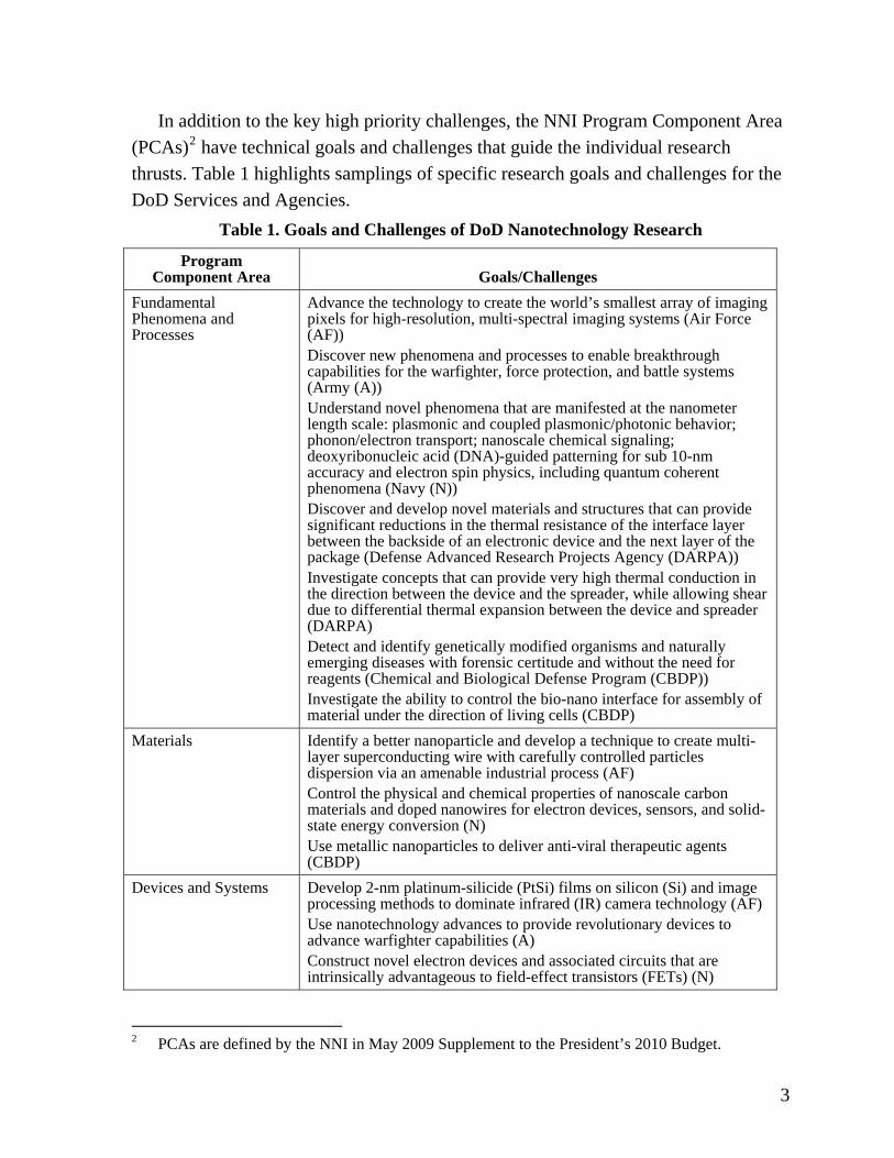
In addition to the key high priority challenges, the NNI Program Component Area (PCAs)2 have technical goals and challenges that guide the individual research thrusts. Table 1 highlights samplings of specific research goals and challenges for the DoD Services and Agencies.
Table 1. Goals and Challenges of DoD Nanotechnology Research
Program Component Area Goals/Challenges
Fundamental Phenomena and Processes
Advance the technology to create the world’s smallest array of imaging pixels for high-resolution, multi-spectral imaging systems (Air Force (AF)) Discover new phenomena and processes to enable breakthrough capabilities for the warfighter, force protection, and battle systems (Army (A)) Understand novel phenomena that are manifested at the nanometer length scale: plasmonic and coupled plasmonic/photonic behavior; phonon/electron transport; nanoscale chemical signaling; deoxyribonucleic acid (DNA)-guided patterning for sub 10-nm accuracy and electron spin physics, including quantum coherent phenomena (Navy (N)) Discover and develop novel materials and structures that can provide significant reductions in the thermal resistance of the interface layer between the backside of an electronic device and the next layer of the package (Defense Advanced Research Projects Agency (DARPA)) Investigate concepts that can provide very high thermal conduction in the direction between the device and the spreader, while allowing shear due to differential thermal expansion between the device and spreader (DARPA) Detect and identify genetically modified organisms and naturally emerging diseases with forensic certitude and without the need for reagents (Chemical and Biological Defense Program (CBDP)) Investigate the ability to control the bio-nano interface for assembly of material under the direction of living cells (CBDP)
Materials Identify a better nanoparticle and develop a technique to create multi-layer superconducting wire with carefully controlled particles dispersion via an amenable industrial process (AF) Control the physical and chemical properties of nanoscale carbon materials and doped nanowires for electron devices, sensors, and solid-state energy conversion (N) Use metallic nanoparticles to deliver anti-viral therapeutic agents (CBDP)
Devices and Systems Develop 2-nm platinum-silicide (PtSi) films on silicon (Si) and image processing methods to dominate infrared (IR) camera technology (AF) Use nanotechnology advances to provide revolutionary devices to advance warfighter capabilities (A) Construct novel electron devices and associated circuits that are intrinsically advantageous to field-effect transistors (FETs) (N)
2 PCAs are defined by the NNI in May 2009 Supplement to the President’s 2010 Budget.
3
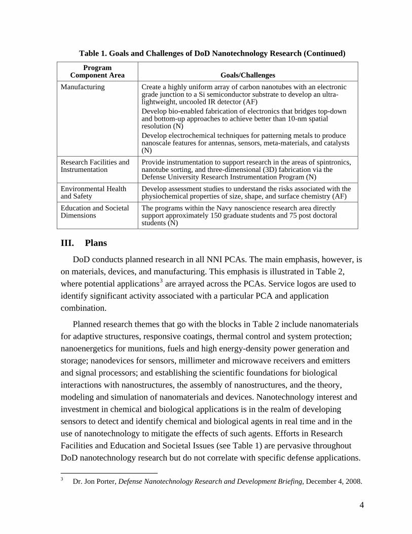
Table 1. Goals and Challenges of DoD Nanotechnology Research (Continued)
Program Component Area Goals/Challenges
Manufacturing Create a highly uniform array of carbon nanotubes with an electronic grade junction to a Si semiconductor substrate to develop an ultra-lightweight, uncooled IR detector (AF) Develop bio-enabled fabrication of electronics that bridges top-down and bottom-up approaches to achieve better than 10-nm spatial resolution (N) Develop electrochemical techniques for patterning metals to produce nanoscale features for antennas, sensors, meta-materials, and catalysts (N)
Research Facilities and Instrumentation
Provide instrumentation to support research in the areas of spintronics, nanotube sorting, and three-dimensional (3D) fabrication via the Defense University Research Instrumentation Program (N)
Environmental Health and Safety
Develop assessment studies to understand the risks associated with the physiochemical properties of size, shape, and surface chemistry (AF)
Education and Societal Dimensions
The programs within the Navy nanoscience research area directly support approximately 150 graduate students and 75 post doctoral students (N)
III. Plans
DoD conducts planned research in all NNI PCAs. The main emphasis, however, is on materials, devices, and manufacturing. This emphasis is illustrated in Table 2, where potential applications3 are arrayed across the PCAs. Service logos are used to identify significant activity associated with a particular PCA and application combination.
Planned research themes that go with the blocks in Table 2 include nanomaterials for adaptive structures, responsive coatings, thermal control and system protection; nanoenergetics for munitions, fuels and high energy-density power generation and storage; nanodevices for sensors, millimeter and microwave receivers and emitters and signal processors; and establishing the scientific foundations for biological interactions with nanostructures, the assembly of nanostructures, and the theory, modeling and simulation of nanomaterials and devices. Nanotechnology interest and investment in chemical and biological applications is in the realm of developing sensors to detect and identify chemical and biological agents in real time and in the use of nanotechnology to mitigate the effects of such agents. Efforts in Research Facilities and Education and Societal Issues (see Table 1) are pervasive throughout DoD nanotechnology research but do not correlate with specific defense applications. 3 Dr. Jon Porter, Defense Nanotechnology Research and Development Briefing, December 4, 2008.
4
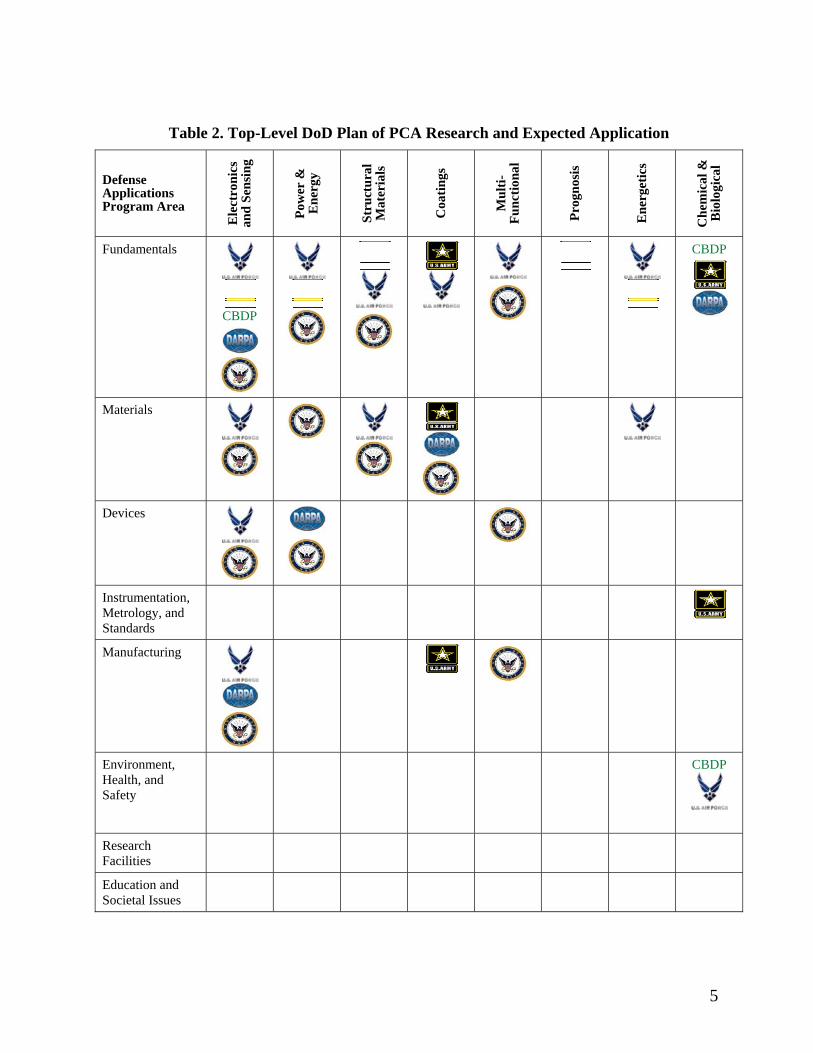
Table 2. Top-Level DoD Plan of PCA Research and Expected Application
Defense Applications Program Area
Ele
ctro
nics
an
d Se
nsin
g
Pow
er &
E
nerg
y
Stru
ctur
al
Mat
eria
ls
Coa
tings
Mul
ti-Fu
nctio
nal
Prog
nosi
s
Ene
rget
ics
Che
mic
al &
B
iolo
gica
l
Fundamentals
CBDP
CBDP
Materials
Devices
Instrumentation, Metrology, and Standards
Manufacturing
Environment, Health, and Safety
CBDP
Research Facilities
Education and Societal Issues
5
IV. Progress
Progress over the past 2 years has led to some promising discoveries and important developments. A sampling of examples arranged by performer and PCA is listed below.4
A. The United States Air Force 1. Air Force Devices and Systems Photon-Plasmon-Electron Conversion Enables a New Class of Imaging
Cameras
This accomplishment conceived and demonstrated a new detector imaging approach that converts photons from an incoming optical signal into surface plasmon waves (as sound waves are produced by oscillating air molecules, plasmons are quantized oscillations of the electron gas in a metal). The plasmon waves are formed in a metal film that is typically less than 100-nm thick and bonded to a semiconductor substrate. The plasmon waves are collected by a slit in the metal film, where their energy is focused to produce electron/hole pairs in the semiconductor. The electron/ hole pairs, in turn, give rise to a measurable electrical signal. Different polarization signals can be produced from the same imaging chip by fabricating different slit orientations, and multi-spectral signals can be produced by fabricating an imaging chip that has several different slit sizes. This accomplishment provides a decrease in detector size of at least 50% relative to existing technology at equivalent resolution. 2. Air Force Nanomaterials Processing of Explosive Formulations With Nano-Aluminum Powder
Munitions enhanced with nano-aluminum powder are being developed to give performance and lethality enhancements in miniaturized munitions needed for the reduced volume of advanced aircraft munitions bays and for weaponization of unmanned air vehicles (UAVs). Munitions using nano-aluminum powder may give improved lethality by improving the airblast and the shrapnel accelerating capability over conventional formulations. Nanoparticles have much higher surface area and are therefore more reactive for a given weight than conventional powders. The reaction rate of nanopowders can be controlled by adjusting the nanoparticle diameter, giving tailorability for optimized airblast and for fragment formation and acceleration. Only 4 Additional reports of progress and other items of DoD interest, especially relating to
environmental safety, can be accessed through the U.S. Air Force newsletter, The Nano Flyer. Available at http://www.nano.gov/html/news/home_news.html.
6
a few percent by volume of nano-aluminum powder could previously be added to munitions formulations, which created a barrier to the development, production, and characterization of advanced munitions with significant additions of nano-aluminum powders. A conventional, castable munitions propellant formulation, which typically has a viscosity similar to honey, is thinned with a solvent so that the nano-aluminum powder can be added. The solvent also desensitizes the formulation so that it is safer to handle during processing. The solvent subsequently vaporizes during blending, leaving a granular formulation with the consistency of brown sugar that can be easily molded to fill munitions containers. Up to 50% by volume of nano-aluminum powder can now be added, compared to only a few percent using previous techniques. An order-of-magnitude improvement in density control is achieved, giving better reproducibility of blast characteristics. Extension of this processing methodology to add nano-aluminum powders to conventional munitions formulations is being pursued at industrial partners, including ATK Thiokol and the Savannah River National Laboratory (SRNL). Performance testing is underway. 3. Air Force Manufacturing Uncooled IR Detector Made Possible With Controlled Carbon Nanotube Array
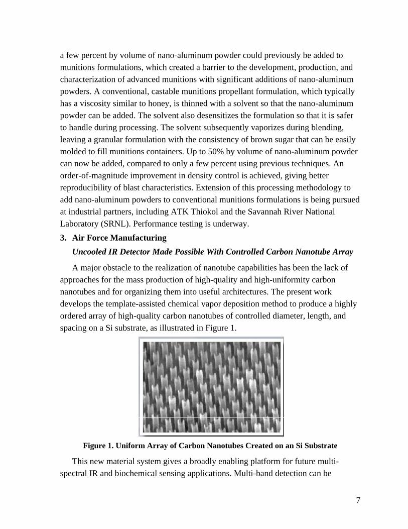
A major obstacle to the realization of nanotube capabilities has been the lack of approaches for the mass production of high-quality and high-uniformity carbon nanotubes and for organizing them into useful architectures. The present work develops the template-assisted chemical vapor deposition method to produce a highly ordered array of high-quality carbon nanotubes of controlled diameter, length, and spacing on a Si substrate, as illustrated in Figure 1.
Figure 1. Uniform Array of Carbon Nanotubes Created on an Si Substrate
This new material system gives a broadly enabling platform for future multi-spectral IR and biochemical sensing applications. Multi-band detection can be
7
achieved over a broad spectral range from near IR to far IR by building arrays with several distinct nanotube diameters that replace several conventional detectors with a single detector array. This capability is important for miniaturization and for providing new sensing capabilities in platforms with limited payloads, such as satellites and UAVs. Nanoparticle Lubricant Produced by Biosynthesis
Biological templates were successfully used to direct the synthesis and assembly of bimetallic nanoparticles. The performance of these nanoparticles was demonstrated as a conductive lubricant in microelectromechanical systems (MEMS) electrical switches at high current with no failure through one million hot-switching cycles. The size, shape, and composition of engineered nanoparticles must be carefully controlled during manufacture to give the needed optical, electronic, catalytic, and mechanical properties. It has recently been shown that biological molecules, such as peptide chains containing up to 20 selected amino acid molecules, can be used to synthesize engineered nanoparticles. This biosynthesis approach is a simple, flexible, real-time manufacturing capability that can produce a wide array of engineered nanoparticles in the field in response to locally identified needs. Potential applications include dechlorination of drinking water, decontamination of nerve agents, and electrically conductive lubricants.
B. The United States Army 1. Army Fundamental Phenomena Photonics
Periodically aligned arrays of carbon nanotubes will be useful for the design of appropriate filters for wavelength division and multiplexing applications. The controlled electrical properties of carbon nanotubes (which can be conductive or semi-conductive), combined with the ability to establish controlled arrays of sizes and spacings, make these materials usefully flexible for filters or signal sorting functions. Piezoelectric Sensing
Studies have shown large changes in the two-dimensional (2D) piezoresistance of electrons confined in quantum wells. Piezoresistance in which the material resistivity is related to dilation has been used for sensing strain, but these materials have often been too stiff for sensitive applications. The technical challenge is to use this effect to create a new family of extremely sensitive strain sensors.
8
Enhanced Thermoelectric Properties
Study of individual nanowires has established that surface states play an important role in determining thermoelectric properties of those wires. The potential to enhance the thermoelectric properties is particularly relevant to Army efforts to develop higher performance, lower power consumption thermoelectric coolers for IR detectors. 2. Army Nanomaterials Improved Polymer Composite
Nano-engineered fiber coatings have been developed to improve the fiber/matrix interface properties of polymer matrix composites. Increased energy absorption while improving or maintaining other composite properties has been demonstrated at the laboratory test specimen level. Chemical Sensing/Decontamination
Basic research has created a class of amplifying fluorescent polymers that detect hazardous substances with extremely high sensitivity. In the same research area, a family of nano-engineered, self-segregating additives that have the ability to transport active materials to the polymer/air interface to self-detoxify contaminated coatings has been developed. 3. Army Devices and Systems Magnetic Resonance Force Microscopy
The magnetic resonance force microscope has demonstrated a spatial resolution of 4 nm. Spatial resolution of conventional magnetic resonance imaging systems is on the order of a few micrometers. Air-Activated Heaters
A nanoparticle composite of zinc and carbon has been developed that self heats via electrochemical oxidation when exposed to air. The heater was developed to heat the standard operational ration meal, ready-to-eat (MRE).
C. The United States Navy 1. Navy Fundamental Phenomena and Processes Electronics
Detection and control of fundamental magnetic spin phenomena will have far-reaching impact in several technologically important areas, most immediately quantum computation. The Navy demonstrated the capability to generate, modulate,
9
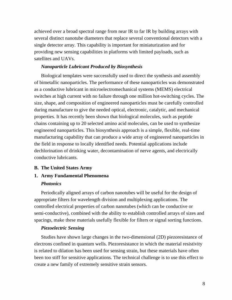
and detect pure electron spin currents in Si for imprinting information into the Si spin system. The ability to control the spin of individual quantum shell states of self-assembled quantum dots by applying a spin-polarized bias current was demonstrated (see Figure 2).
Figure 2. Generating, Modulating, and Electrically Detecting Pure Spin Currents
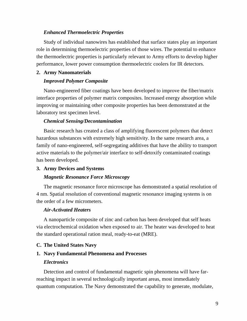
A “quantum dot thermometry” technique was established to measure temperature gradients across very small distances and distinguish between electronic and lattice vibration contributions to thermal transport (see Figure 3).
(a) (b)
40 n
m40
nm
nanowire
source contac
Figure 3. Quantum Dot Thermometry Note for Figure 3: (a) Scanning electron microscopy (SEM) image of the InAs nanowire with source contact (SC), drain contact (DC), and InP/InAs/InP quantum dot (QD) embedded in nanowire is shown in the inset; (b) schematic (not to scale) temperature profile along a nanowire embedded QD, a heated SC, and an unheated DC.
tdrain
contac15 nm quantum dot
(5 nm barriers) t
10
Fundamental Thermal Properties
The quantum dot thermometry accomplishment has application to many areas, as does most fundamental science research, but emerged from the fundamental thermoelectrics studies of nanowires. Nanostructure-Enhanced Thermoelectric Properties
The ability to partially decouple phonon and electron transport through the design of composite semiconductor systems incorporating epitaxial nanoparticles has been experimentally demonstrated in nano-structured nanowires, thin films, and bulk materials. Theoretical models support the nanoparticle size-dependent reduction of thermal conductivity with minimal impact on electrical conductivity that has led to record thermoelectric performance in these materials. Higher efficiency, solid-state energy conversion applications enabled by these advances include fuel-flexible, portable power generation, vehicle waste heat recuperation/fuel efficiency, and electronic device/systems cooling. 2. Navy Nanomaterials Magnetics
A cobalt-rich, nanocrystalline alloy that had significantly enhanced fracture toughness over conventional iron based magnetic alloys was developed. Yield rates for the fabrication of complex magnetic components can be as low as 20%. Damage-resistant magnetic materials offer expanded motor design options with significantly reduced manufacturing costs. Semiconductors
The first discrete quaternary nanocrystal, AgPbmSbTem+2 (m = 1-18), has been synthesized by a low-temperature solution route and demonstrates a new approach to achieve homogeneous solid-solution alloys with size- and composition-controlled semiconductor properties otherwise unobtainable in the bulk. This class of semiconductor nanocrystals has potential applications in thermoelectric energy conversion, IR sensing, phase change memory, and photovoltaics. 3. Navy Devices and Systems Spin-Based Devices
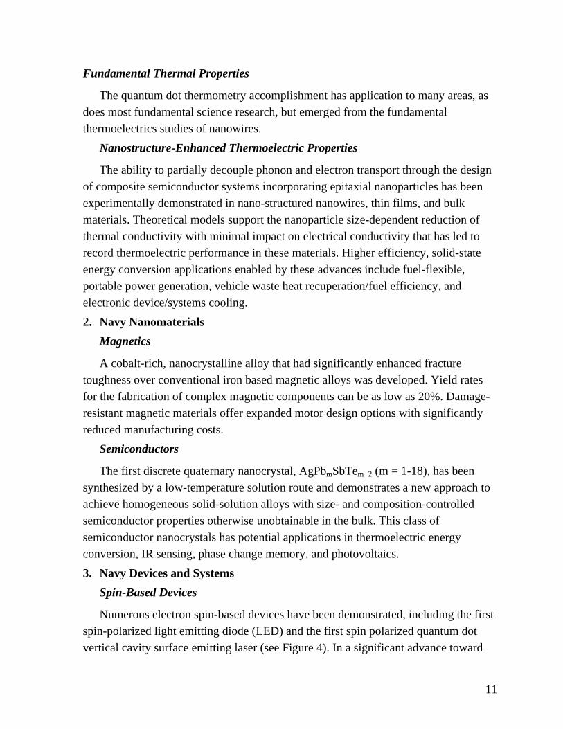
Numerous electron spin-based devices have been demonstrated, including the first spin-polarized light emitting diode (LED) and the first spin polarized quantum dot vertical cavity surface emitting laser (see Figure 4). In a significant advance toward
11
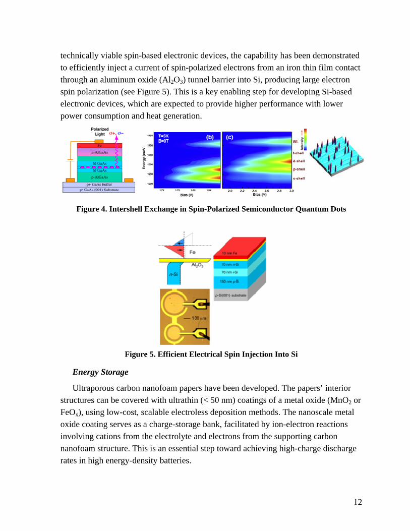
technically viable spin-based electronic devices, the capability has been demonstrated to efficiently inject a current of spin-polarized electrons from an iron thin film contact through an aluminum oxide (Al2O3) tunnel barrier into Si, producing large electron spin polarization (see Figure 5). This is a key enabling step for developing Si-based electronic devices, which are expected to provide higher performance with lower power consumption and heat generation.
Figure 4. Intershell Exchange in Spin-Polarized Semiconductor Quantum Dots
Figure 5. Efficient Electrical Spin Injection Into Si
Energy Storage
Ultraporous carbon nanofoam papers have been developed. The papers’ interior structures can be covered with ultrathin (< 50 nm) coatings of a metal oxide (MnO2 or FeOx), using low-cost, scalable electroless deposition methods. The nanoscale metal oxide coating serves as a charge-storage bank, facilitated by ion-electron reactions involving cations from the electrolyte and electrons from the supporting carbon nanofoam structure. This is an essential step toward achieving high-charge discharge rates in high energy-density batteries.
12
4. Navy Instrumentation/Metrology/Standards Mechanical Property Variation
The Navy developed an instrument that combined the imaging capability of scanning probe microscopy with the nanomechanical measurement capabilities of instrumented indentation to create a capability to image variation of mechanical properties and topography within the test specimen. This tool will enable researchers to probe the mechanisms that determine response of nanocomposites to stress at the appropriate length scales, ultimately guiding the design of more efficient structural composites for realistic naval applications. 5. Navy Nanomanufacturing Cost Saving
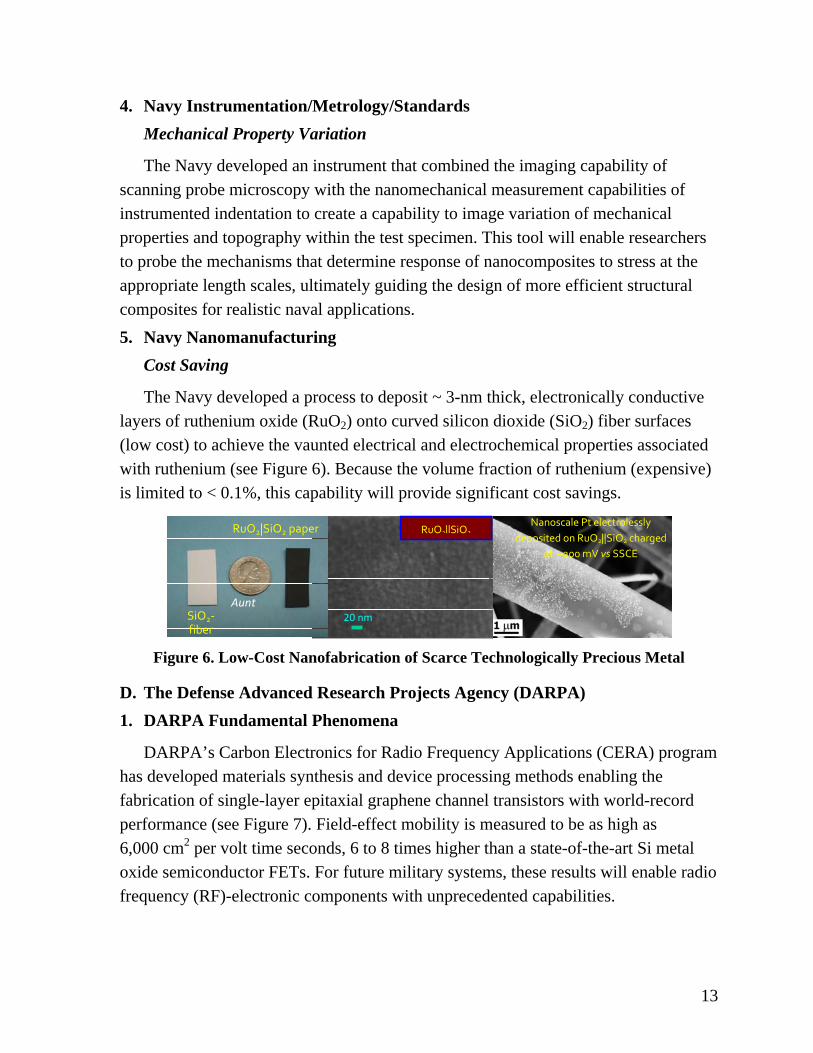
The Navy developed a process to deposit ~ 3-nm thick, electronically conductive layers of ruthenium oxide (RuO2) onto curved silicon dioxide (SiO2) fiber surfaces (low cost) to achieve the vaunted electrical and electrochemical properties associated with ruthenium (see Figure 6). Because the volume fraction of ruthenium (expensive) is limited to < 0.1%, this capability will provide significant cost savings.
Nanoscale Pt electrolessly deposited on RuO2||SiO2 charged
at –200 mV vs SSCE
20 nm
RuO2||SiO2
Aunt SiO2‐fiber
RuO2||SiO2 paper
Figure 6. Low-Cost Nanofabrication of Scarce Technologically Precious Metal
D. The Defense Advanced Research Projects Agency (DARPA) 1. DARPA Fundamental Phenomena
DARPA’s Carbon Electronics for Radio Frequency Applications (CERA) program has developed materials synthesis and device processing methods enabling the fabrication of single-layer epitaxial graphene channel transistors with world-record performance (see Figure 7). Field-effect mobility is measured to be as high as 6,000 cm2 per volt time seconds, 6 to 8 times higher than a state-of-the-art Si metal oxide semiconductor FETs. For future military systems, these results will enable radio frequency (RF)-electronic components with unprecedented capabilities.
13
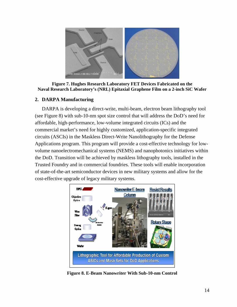
Figure 7. Hughes Research Laboratory FET Devices Fabricated on the
Naval Research Laboratory’s (NRL) Epitaxial Graphene Film on a 2-inch SiC Wafer
2. DARPA Manufacturing
DARPA is developing a direct-write, multi-beam, electron beam lithography tool (see Figure 8) with sub-10-nm spot size control that will address the DoD’s need for affordable, high-performance, low-volume integrated circuits (ICs) and the commercial market’s need for highly customized, application-specific integrated circuits (ASCIs) in the Maskless Direct-Write Nanolithography for the Defense Applications program. This program will provide a cost-effective technology for low-volume nanoelectromechanical systems (NEMS) and nanophotonics initiatives within the DoD. Transition will be achieved by maskless lithography tools, installed in the Trusted Foundry and in commercial foundries. These tools will enable incorporation of state-of-the-art semiconductor devices in new military systems and allow for the cost-effective upgrade of legacy military systems.
Figure 8. E-Beam Nanowriter With Sub-10-nm Control
14
E. The Defense Threat Reduction Agency (DTRA) 1. DTRA Chem/Bio (CB) Defense Functional Nanostructures
DTRA-CB is developing computational methods for predicting the physical and chemical properties of DNA-coated nanoparticles. This technology will replace current Edisonian (i.e., trial and error) approaches and enable the a priori design of nano-structured materials with tailored characteristics, such as molecular recognition, catalysis, and signal transduction. Currently funded programs include the design of artificial membranes and synthetic receptors that will be used to construct robust sensors for chemical, biological, explosive and radiological detection. 2. DTRA CB Defense Biomimetic Design Rules
DTRA-CB is using the principles elucidated from bacterial communication circuitry to develop minimal biological circuits that will form the bases for the bottom-up design and assembly of bioelectronic circuitry. In addition, the design rules for the self-assembly of protein nanostructures are being investigated. Elucidation of such first principles of biological design will enable the design and assembly of complex molecular machines that can be incorporated into materials (e.g., fabrics and coatings) to give them a range of functionalities such as selective porosity, catalysis, information processing and the ability to alter structure and color in response to environmental conditions. 3. DTRA CB Defense Nanoscale Platforms
DTRA-CB is developing nanoscale platforms to enable DNA cloning without the use of cells. A related program uses nanoscale polymerase chain reaction (nano-PCR) with a focus on ultrasensitive, rapid, high-fidelity identification of natural or genetically engineered pathogen strains. These programs will have sensitivities three orders of magnitude better than conventional PCR, permitting single molecule amplification from complex (i.e. dirty) environmental samples. 4. DTRA CB Smart Hazard Mitigation
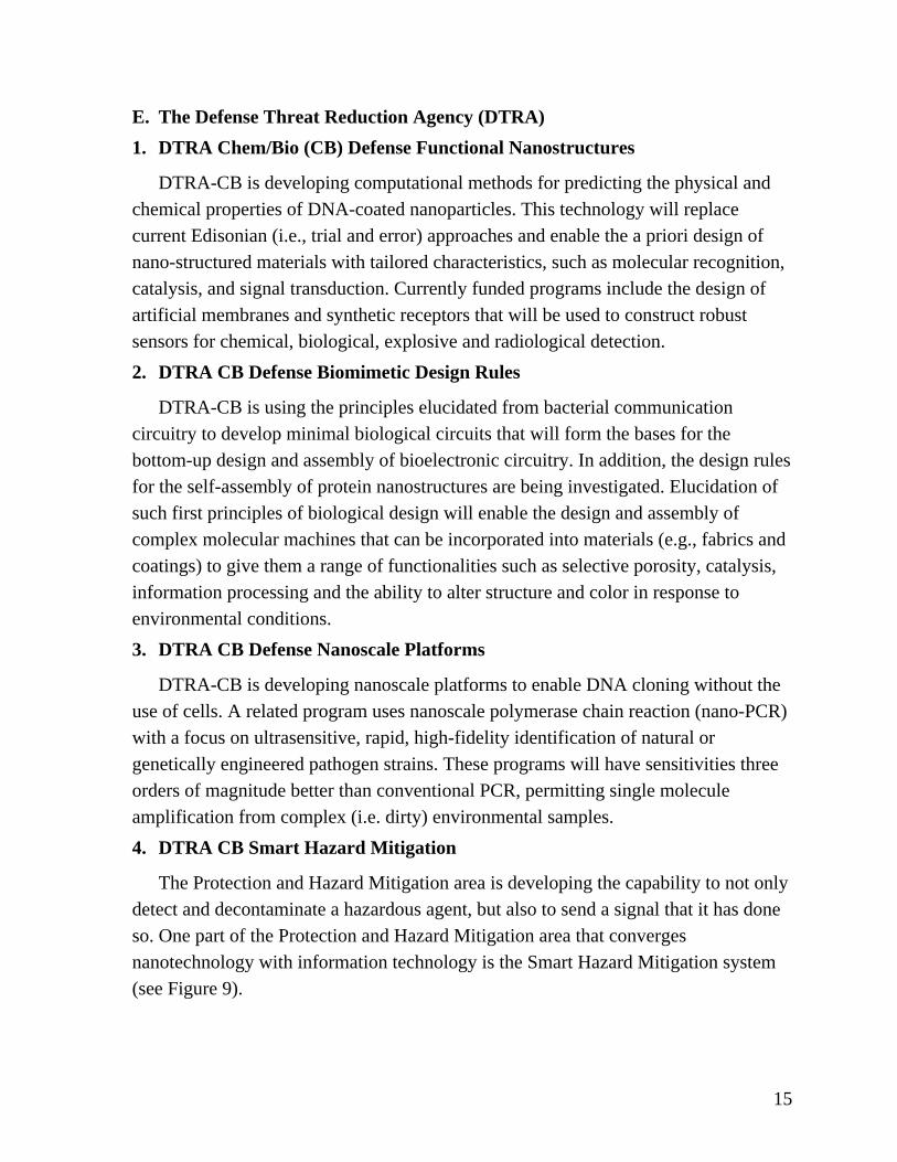
The Protection and Hazard Mitigation area is developing the capability to not only detect and decontaminate a hazardous agent, but also to send a signal that it has done so. One part of the Protection and Hazard Mitigation area that converges nanotechnology with information technology is the Smart Hazard Mitigation system (see Figure 9).
15
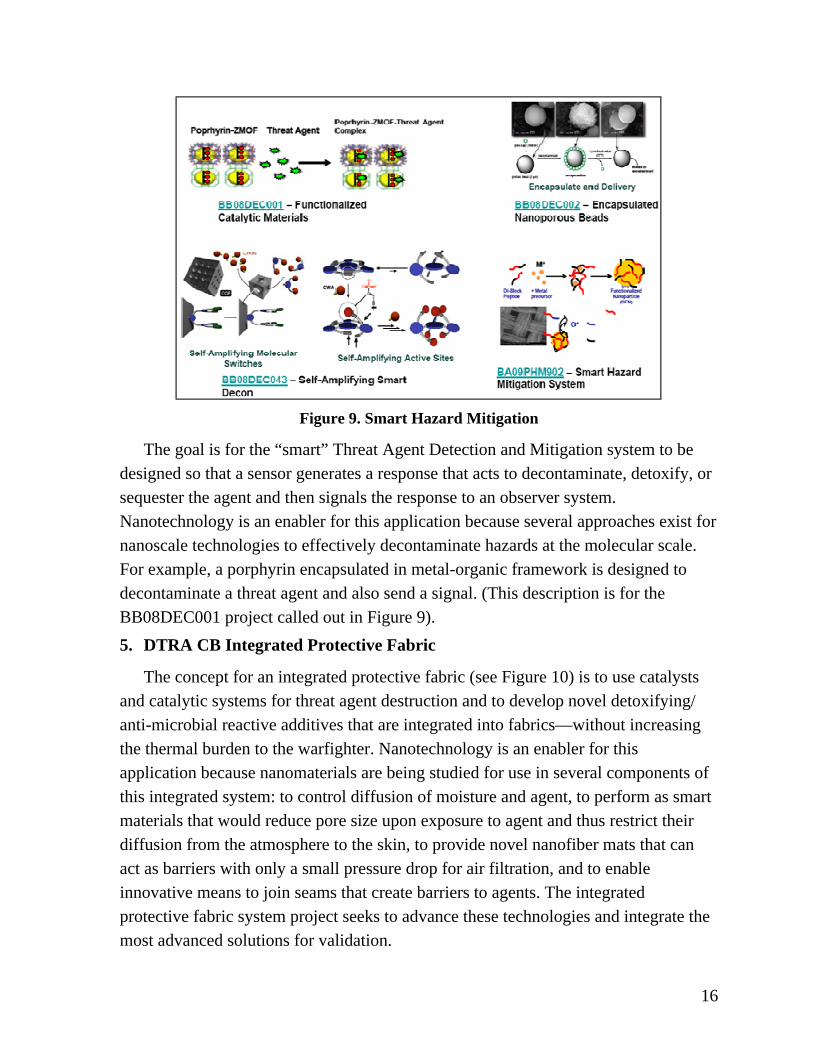
Figure 9. Smart Hazard Mitigation
The goal is for the “smart” Threat Agent Detection and Mitigation system to be designed so that a sensor generates a response that acts to decontaminate, detoxify, or sequester the agent and then signals the response to an observer system. Nanotechnology is an enabler for this application because several approaches exist for nanoscale technologies to effectively decontaminate hazards at the molecular scale. For example, a porphyrin encapsulated in metal-organic framework is designed to decontaminate a threat agent and also send a signal. (This description is for the BB08DEC001 project called out in Figure 9). 5. DTRA CB Integrated Protective Fabric
The concept for an integrated protective fabric (see Figure 10) is to use catalysts and catalytic systems for threat agent destruction and to develop novel detoxifying/ anti-microbial reactive additives that are integrated into fabrics—without increasing the thermal burden to the warfighter. Nanotechnology is an enabler for this application because nanomaterials are being studied for use in several components of this integrated system: to control diffusion of moisture and agent, to perform as smart materials that would reduce pore size upon exposure to agent and thus restrict their diffusion from the atmosphere to the skin, to provide novel nanofiber mats that can act as barriers with only a small pressure drop for air filtration, and to enable innovative means to join seams that create barriers to agents. The integrated protective fabric system project seeks to advance these technologies and integrate the most advanced solutions for validation.
16
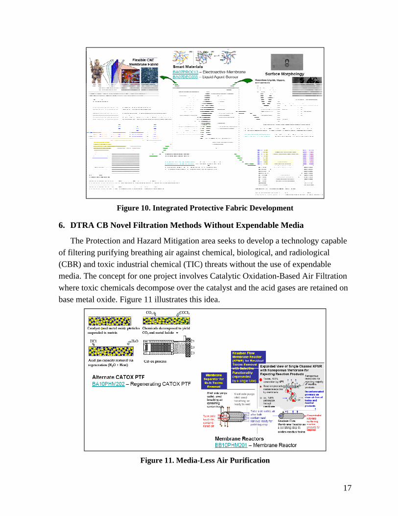
Figure 10. Integrated Protective Fabric Development
6. DTRA CB Novel Filtration Methods Without Expendable Media
The Protection and Hazard Mitigation area seeks to develop a technology capable of filtering purifying breathing air against chemical, biological, and radiological (CBR) and toxic industrial chemical (TIC) threats without the use of expendable media. The concept for one project involves Catalytic Oxidation-Based Air Filtration where toxic chemicals decompose over the catalyst and the acid gases are retained on base metal oxide. Figure 11 illustrates this idea.
Figure 11. Media-Less Air Purification
17
V. Funding
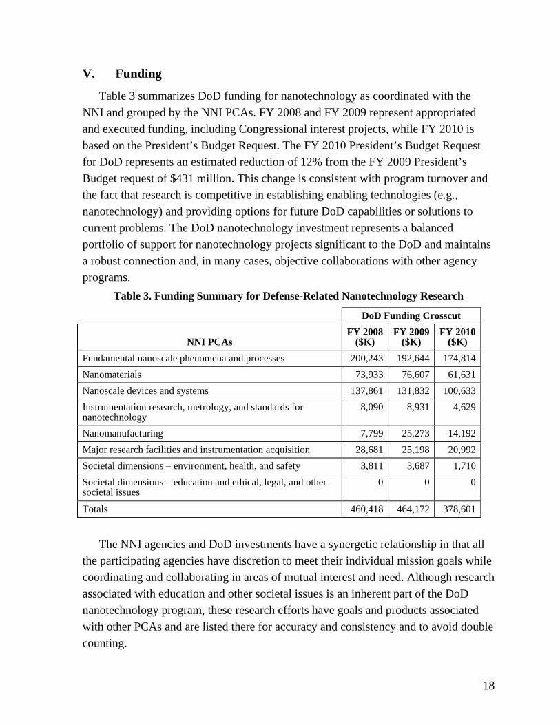
Table 3 summarizes DoD funding for nanotechnology as coordinated with the NNI and grouped by the NNI PCAs. FY 2008 and FY 2009 represent appropriated and executed funding, including Congressional interest projects, while FY 2010 is based on the President’s Budget Request. The FY 2010 President’s Budget Request for DoD represents an estimated reduction of 12% from the FY 2009 President’s Budget request of $431 million. This change is consistent with program turnover and the fact that research is competitive in establishing enabling technologies (e.g., nanotechnology) and providing options for future DoD capabilities or solutions to current problems. The DoD nanotechnology investment represents a balanced portfolio of support for nanotechnology projects significant to the DoD and maintains a robust connection and, in many cases, objective collaborations with other agency programs.
Table 3. Funding Summary for Defense-Related Nanotechnology Research
DoD Funding Crosscut
NNI PCAs FY 2008
($K) FY 2009
($K) FY 2010
($K) Fundamental nanoscale phenomena and processes 200,243 192,644 174,814Nanomaterials 73,933 76,607 61,631Nanoscale devices and systems 137,861 131,832 100,633Instrumentation research, metrology, and standards for nanotechnology
8,090 8,931 4,629
Nanomanufacturing 7,799 25,273 14,192Major research facilities and instrumentation acquisition 28,681 25,198 20,992Societal dimensions – environment, health, and safety 3,811 3,687 1,710Societal dimensions – education and ethical, legal, and other societal issues
0 0 0
Totals 460,418 464,172 378,601
The NNI agencies and DoD investments have a synergetic relationship in that all
the participating agencies have discretion to meet their individual mission goals while coordinating and collaborating in areas of mutual interest and need. Although research associated with education and other societal issues is an inherent part of the DoD nanotechnology program, these research efforts have goals and products associated with other PCAs and are listed there for accuracy and consistency and to avoid double counting.
18
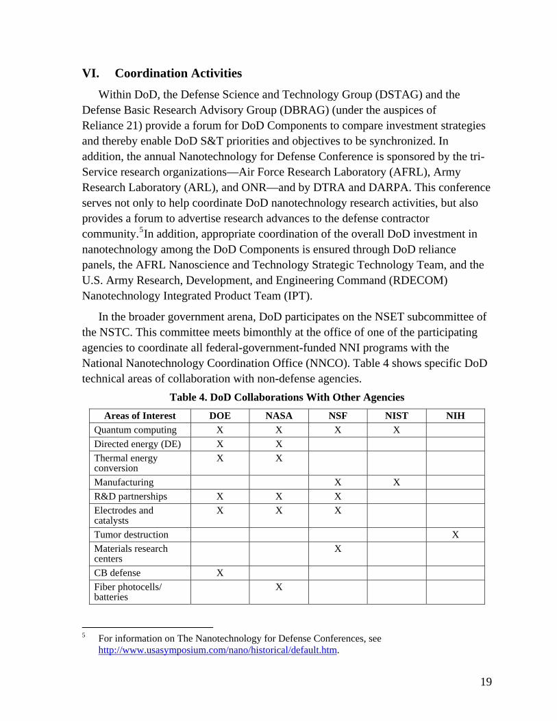
VI. Coordination Activities
Within DoD, the Defense Science and Technology Group (DSTAG) and the Defense Basic Research Advisory Group (DBRAG) (under the auspices of Reliance 21) provide a forum for DoD Components to compare investment strategies and thereby enable DoD S&T priorities and objectives to be synchronized. In addition, the annual Nanotechnology for Defense Conference is sponsored by the tri-Service research organizations—Air Force Research Laboratory (AFRL), Army Research Laboratory (ARL), and ONR—and by DTRA and DARPA. This conference serves not only to help coordinate DoD nanotechnology research activities, but also provides a forum to advertise research advances to the defense contractor community.5In addition, appropriate coordination of the overall DoD investment in nanotechnology among the DoD Components is ensured through DoD reliance panels, the AFRL Nanoscience and Technology Strategic Technology Team, and the U.S. Army Research, Development, and Engineering Command (RDECOM) Nanotechnology Integrated Product Team (IPT).
In the broader government arena, DoD participates on the NSET subcommittee of the NSTC. This committee meets bimonthly at the office of one of the participating agencies to coordinate all federal-government-funded NNI programs with the National Nanotechnology Coordination Office (NNCO). Table 4 shows specific DoD technical areas of collaboration with non-defense agencies.
Table 4. DoD Collaborations With Other Agencies
Areas of Interest DOE NASA NSF NIST NIH Quantum computing X X X X Directed energy (DE) X X Thermal energy conversion
X X
Manufacturing X X R&D partnerships X X X Electrodes and catalysts
X X X
Tumor destruction X Materials research centers
X
CB defense X Fiber photocells/ batteries
X
5 For information on The Nanotechnology for Defense Conferences, see http://www.usasymposium.com/nano/historical/default.htm.
19
VII. DoD Implementation of Triennial Review Recommendations
A 2006 National Academies report, A Matter of Size: Triennial Review of the National Nanotechnology Initiative, made several recommendations to the NSET that also relate to DoD programs. DoD activities and management processes contribute directly and appropriately to fulfilling two of these recommendations.
The National Academy report recommended that “the federal government sustain investments in a manner that balances the pursuit of shorter term goals with support for longer term R&D and that ensures a robust supporting infrastructure, broadly defined” (p. 7).
DoD’s Basic Research, Applied Research, and Advanced Technology Development categorization and process for planning and execution essentially addresses the issue of balancing long-term, knowledge-driven goals with development aimed at shorter term technology maturation to support entry into technology transition. Historically, DoD’s Technology Base (Budget Activity 1–3) investment in nanotechnology has been approximately 50% Basic Research, about 40% Applied Research, and about 10% Advanced Technology Development. The bulk of the Small Business Innovation Research (SBIR)/Small Business Technology Transfer (STTR) investment in nanotechnology would be categorized as functionally similar to Applied Research, although with a strong, direct commercializable product or process aspect more analogous to Advanced Technology Development. The current expectation is that these overall percentages will be continued through FY 2010. As nanotechnology research area and tools providers continue to mature, we can expect to see growth in Applied Research and Advanced Technology Development efforts. Maturation of specific products in commercial programs often occurs because of DoD-supported Basic and Applied Research efforts that have increased the knowledge and general technology base. For this reason, continued robust support for foundational research in an area that can be valuable to DoD and the nation is important.
The National Academies report also recommended that “research on the environmental, health, and safety effects of nanotechnology be expanded” (p. 11).
Although the DoD has not been the lead agency in the environmental, health, and safety areas of research, it has continued to support projects that relate to environmental, health, and safety issues in its mission portfolio. It is working closely with NSET and the working groups, including the Nanotechnology Environmental Safety and Health Implications Working Group, and is actively seeking additional
20
collaborative opportunities in this area with other federal agencies. DoD considers environmental, health, and safety to be intrinsic and pervasive issues in all nanotechnology research and in the responsible application of nanotechnology to products. As an example, the Air Force has developed compulsory guidelines for the safe handling of nanomaterials and for performing research associated with nanotechnology.6
VIII. Assessment of Technology Transition
Each of the Services coordinates the exploration of nanotechnology and identifies rapid and effective technology transition paths through the DoD reliance panels and other research teams (e.g., the AFRL Nanoscience and Technology Strategic Technology Team and the U.S. Army RDECOM Nanotechnology IPT).
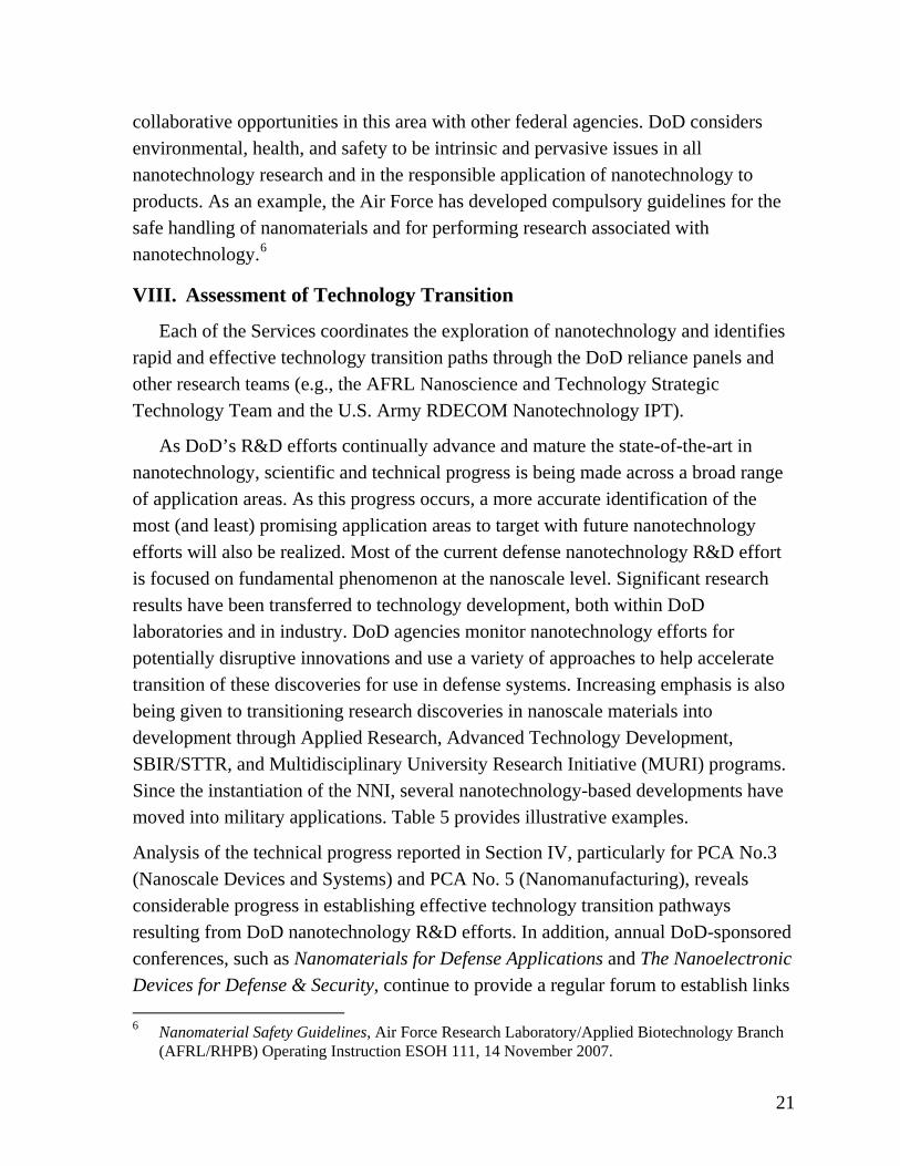
As DoD’s R&D efforts continually advance and mature the state-of-the-art in nanotechnology, scientific and technical progress is being made across a broad range of application areas. As this progress occurs, a more accurate identification of the most (and least) promising application areas to target with future nanotechnology efforts will also be realized. Most of the current defense nanotechnology R&D effort is focused on fundamental phenomenon at the nanoscale level. Significant research results have been transferred to technology development, both within DoD laboratories and in industry. DoD agencies monitor nanotechnology efforts for potentially disruptive innovations and use a variety of approaches to help accelerate transition of these discoveries for use in defense systems. Increasing emphasis is also being given to transitioning research discoveries in nanoscale materials into development through Applied Research, Advanced Technology Development, SBIR/STTR, and Multidisciplinary University Research Initiative (MURI) programs. Since the instantiation of the NNI, several nanotechnology-based developments have moved into military applications. Table 5 provides illustrative examples.
Analysis of the technical progress reported in Section IV, particularly for PCA No.3 (Nanoscale Devices and Systems) and PCA No. 5 (Nanomanufacturing), reveals considerable progress in establishing effective technology transition pathways resulting from DoD nanotechnology R&D efforts. In addition, annual DoD-sponsored conferences, such as Nanomaterials for Defense Applications and The Nanoelectronic Devices for Defense & Security, continue to provide a regular forum to establish links 6 Nanomaterial Safety Guidelines, Air Force Research Laboratory/Applied Biotechnology Branch
(AFRL/RHPB) Operating Instruction ESOH 111, 14 November 2007.
21
between DoD-funded R&D efforts and commercial and defense product developers, which are often the same because of the dual-use nature of most nanotechnology research at this time.
Table 5. Successful Transitions of Nanotechnology-Based Products Into Defense Products
Effort Accomplishment Impact Coating for High Power Microwave (HPM) Devices (AF)
New cathode with 100-nm cesium iodide (CsI) coating
Reduces HPM system size, weight, and power consumption
Nanocomposite Space System Insulation (AF)
Nano-structured silicate molecules were developed and commercialized for rocket motor insulation
Reduced rocket motor insulation weight and increased erosion resistance; material cost reduced from $1,000/lb to $20/lb
Dual-Band Quantum Well IR Camera (AF)
Unique quantum well architecture to develop an IR detector operating in the long wave infrared (LWIR)/LWIR regime
Provide basis for development of a follow on LWIR/medium wave infrared (MWIR) camera with improved sensitivity.
Fido TNT Sensor (A) Novel amplifying fluorescent polymers that sense ultratrace concentrations of nitroaromatics
First man-made sensor with the sensitivity to detect buried landmines by their chemical signature; is small, man-portable, uses little power; is inexpensive to produce
Nano-structured Alumina/Titania Coatings (N)
Improved wear-resistant coatings for bearings and valves
Coating lifetime extended from hours to years based on preliminary analysis
IX. Assessment of Small Business and Manufacturing Technology Contributions and Transitions
The DoD SBIR/STTR programs and ManTech (i.e., product- and manufacturing-technology-based) programs are poised to transition valuable results to military and commercial products. A search of the DoD 2008 SBIR/STTR awards database identified 48 SBIR projects and 15 STTR projects based on nanotechnology7. Table 6 shows a financial summary of SBIR/STTR Phase 1 and Phase 2 programs awarded by DoD component for 2008.
Overall, SBIR program project values were nearly $20 million and STTRs constituted another $2.3 million. SBIR and STTR programs all fall in the general categories of Nanomaterials and Nanoscale Devices and Systems under the categories shown in Table 3. Those two budget subcategories for 2008 totaled approximately 7 2008 is the most recent year in which complete SBIR/STTR data are available.
22
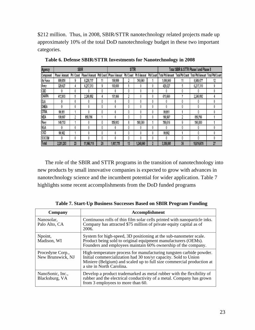
$212 million. Thus, in 2008, SBIR/STTR nanotechnology related projects made up approximately 10% of the total DoD nanotechnology budget in these two important categories.
Table 6. Defense SBIR/STTR Investments for Nanotechnology in 2008
The role of the SBIR and STTR programs in the transition of nanotechnology into new products by small innovative companies is expected to grow with advances in nanotechnology science and the incumbent potential for wider application. Table 7 highlights some recent accomplishments from the DoD funded programs
Table 7. Start-Up Business Successes Based on SBIR Program Funding
Company Accomplishment Nanosolar, Palo Alto, CA
Continuous rolls of thin film solar cells printed with nanoparticle inks. Company has attracted $75 million of private equity capital as of 2006.
Npoint, Madison, WI
System for high-speed, 3D positioning at the sub-nanometer scale. Product being sold to original equipment manufacturers (OEMs). Founders and employees maintain 60% ownership of the company.
Procedyne Corp., New Brunswick, NJ
High-temperature process for manufacturing tungsten carbide powder. Initial commercialization had 30 ton/yr capacity. Sold to Union Miniere (Belgium) and scaled up to full size commercial production at a site in North Carolina.
NanoSonic, Inc., Blacksburg, VA
Develop a product trademarked as metal rubber with the flexibility of rubber and the electrical conductivity of a metal. Company has grown from 3 employees to more than 60.
23
X. Acquisition Program and Program Office Status
The military applications envisioned for nanotechnology are numerous and growing as fundamental research and applied research reveal ever more possibilities. As previously shown in Table 5, several nanotechnology-based developments have moved into military applications since instantiation of the NNI. These developments represent specific and pervasive applications that are benefiting Defense acquisition.
We should note, however, that DoD acquisition programs have not been significantly associated with the maturation of nanotechnology for specific program items. The transitions have largely been associated with product enhancements within the industrial base, including DoD research products inserted through and by OEMs and sub-tier suppliers. As the Technology Readiness Levels (TRLs) of nanotechnology-based products increase, we can expect to see more direct maturation become a part of acquisition programs.
XI. Global Research Activities8
Trying to determine what applications will reap the greatest benefits from specific nanoscience projects is often difficult. Consequently, unless the funding source is revealed, the nanoscience research projects designed to meet military needs are often not obvious. For some defense-oriented foreign countries, notably Israel, intentions to develop nanotechnology for defense applications are well known and publicized. Unfortunately, most countries are not as transparent (in revealing the defense-oriented nature of funding) as the United States and Israel, making it necessary to follow overall government spending on nanotechnology (where possible) to assess the overall strength of the nanoscience research sector of foreign countries.
The major international players in nanoscience research are the United States, the European Union (EU), the Peoples Republic of China (PRC), Japan, and the Asian Tiger Economies of Singapore, South Korea, and Taiwan. The United States and the EU have stood at the forefront of nanoscience, in terms of quantity and quality of research since the birth of the field. The most compelling story of recent years, however, has been the emergence of the PRC and the Asian Tigers. Government initiatives and funding, coupled with foreign investment, are major drivers for this
8 Input extracted from “Global Defense-Related Nanotechnology Research and Development” by
Shawn Thorne, Office of Naval Research Global, June 11, 2009.
24
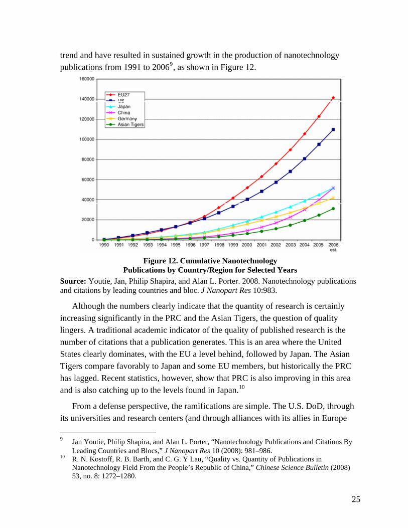
trend and have resulted in sustained growth in the production of nanotechnology publications from 1991 to 20069, as shown in Figure 12.
Figure 12. Cumulative Nanotechnology
Publications by Country/Region for Selected Years Source: Youtie, Jan, Philip Shapira, and Alan L. Porter. 2008. Nanotechnology publications and citations by leading countries and bloc. J Nanopart Res 10:983.
Although the numbers clearly indicate that the quantity of research is certainly increasing significantly in the PRC and the Asian Tigers, the question of quality lingers. A traditional academic indicator of the quality of published research is the number of citations that a publication generates. This is an area where the United States clearly dominates, with the EU a level behind, followed by Japan. The Asian Tigers compare favorably to Japan and some EU members, but historically the PRC has lagged. Recent statistics, however, show that PRC is also improving in this area and is also catching up to the levels found in Japan.10
From a defense perspective, the ramifications are simple. The U.S. DoD, through its universities and research centers (and through alliances with its allies in Europe 9 Jan Youtie, Philip Shapira, and Alan L. Porter, “Nanotechnology Publications and Citations By
Leading Countries and Blocs,” J Nanopart Res 10 (2008): 981–986. 10 R. N. Kostoff, R. B. Barth, and C. G. Y Lau, “Quality vs. Quantity of Publications in
Nanotechnology Field From the People’s Republic of China,” Chinese Science Bulletin (2008) 53, no. 8: 1272–1280.
25
and Japan), has access to much of the best nanotechnology in the world. If the global trends continue, however, this situation may not necessarily be the case in the future.
The EU, as a whole, publishes the most nanotechnology-related publications (as a region) and features some of the best nano-research and nano-dedicated laboratories in the world. The EU excels across the spectrum of sub-disciplines within nanotechnology but especially in certain areas of nanosynthesis and nanolithography, where it is at least on a par with the United States.
While China does not have a prescribed national nanotechnology initiative, its nanotechnology efforts are supported by formalized plans issued from the highest levels of the government. China increased funding five-fold during 2003–2007 as compared to the previous 5 years. The country’s programs are broad-based, comprehensive, and long term, including standardization efforts, environmental discussions, and toxicity research. China has also instituted a vigorous and successful effort in international cooperation. Figure 12 shows that China was the third leading producer of journal articles by the end of 2006.
A. Nanotechnology: China
In 2003, the Chinese Academy of Sciences revealed that China was investing nearly as much on National Defense as on the entire topic area of nanomaterials. However, the level of investment is not clear.
Chinese authors have published numerous technical journal reports on nanotechnology research that has a high likelihood of military use, including nanoparticles research for energetic applications, structural materials for extreme environments, electromagnetic absorbers, and armor.
The PRC ranks only slightly behind the United States in terms of annual national nanotechnology publications. Government investment in nanotechnology is significant, but, unfortunately, the specific defense contributions are unknown. Nanotechnology represents one of the PRC’s mega science projects and evinces the following:
• National Center for Nanoscience and Technology founded in Beijing in 2004 • National Center for Promoting and Developing Nanotechnology in Shanghai • 50 universities, 20 China Academy of Sciences Institutes, and 800 companies
active in the research area • Over 4,500 researchers.
26
The PRC considers nanotechnology an area of research in which they are playing on a level field with the United States. In 2004, PRC researchers captured a 16% share in nano-related publications, only 5 years after the research area had been made a national S&T priority. The PRC has major programs in the following areas:
• Synthesis and characterization of low-dimensional nanostructures • Nanomagnets (such as the type used in the Maglev) • Molecular electronics • Photocatalytic and photoelectric chemistry of nanosemiconductors • Bond-selective chemistry • Manipulation of single atoms.
All these programs rival the United States. In particular, Tsinghua University, Fudan University, Jiao Tong University, Chinese Academy of Sciences, Beijing University, Nanjing University, and East University of Science and Technology have particularly accomplished nanotechnology programs.
B. Nanotechnology: Japan
Nanotechnology R&D in Japan is directed toward approved priority research areas, according to the Science and Technology Basic Plan. The bulk of funding for nanotechnology R&D is administered by the Ministry of Economy, Trade, and Industry (METI) and the Ministry of Education, Culture, Sports, Science and Technology (MEXT). From 2001 through 2004, METI and MEXT combined for $2.4 billion in funding for nanotechnology and materials R&D. Japan has a large focus on carbon nanomaterials, leveraging its strength in carbon fibers.
Japan’s nanotechnology is considered roughly equivalent with U.S. efforts in the area of semiconductor and inorganic nanostructures. Most of the nanotechnology research in Japan is supported under the Ministry of International Trade and Industry (MITI) with the main thrust being the development of future-generation computer chips. Japan is undertaking a massive amount of research in areas related to advanced computer chip technology. Informed sources estimate that there are probably more advanced materials fabrication systems in both NTT Atsugi laboratories and Fujitsu’s Quantum Electron Devices Laboratory than in the whole of Europe. Japan’s other
11 Government of Japan, Science & Technology Basic Plan, (28 March 2006), 3. 12 Teruo Kishi, “Nanotechnology R&D Policy of Japan and Nanotechnology Support Project,”
Journal of Nanoparticle Research (28 October 2004): 1. 13 Teruo Kishi, “Nanotechnology R&D Policy of Japan and Nanotechnology Support Project,”
Journal of Nanoparticle Research, (28 October 2004): 1.
27
electronics giants—Hitachi, Matsushita, Mitsubishi, NEC, Sony, Sumitomo Electric, and Toshiba—and numerous smaller companies are also working on quantum devices. Main research areas are in resonant tunneling devices, Coulomb effect devices, and the entire family of “quantum effect devices.” As warfare becomes more and more dependent on computers, these efforts have increasing defense relevance.
Through MITI and New Energy and Industrial Technology Development Organization (NEDO), Japan has several government-funded nanotechnology-related projects. Of note are the following:
• Quantum functional devices. To design and fabricate highly functional quantum devices, such as titanium-oxide (TiOx) quantum wires of 18-nm width using a scanning tunneling microscope.
• Bioelectronic devices. To analyze essential principles followed in learning, memorization, and pattern recognition in biological nerve systems such as “bio-computer.”
• Femtosecond technology project. To develop ultrafast information processing and communication technology through better understanding of physical phenomena in the femtosecond range. Applications are ultrafast measurement, environmental measurement, and medical applications.
• Ultimate manipulation of atoms and molecules. To develop technology for exactly observing and identifying atoms and molecules and arranging them in a desired layout. The end product can be the possibility of creating new materials through the control of materials structures at atomic and molecular levels.
• Yamamoto quantum fluctuation project. Collaboration between NTT Basic Research Laboratory and Stanford University to conduct research on quantum measurements and quantum computers.
The major nanotechnology-related projects in Japan are as follows:
• RIKEN – Frontier Materials Research Program • ERATO – Nanostructure Research Program • JRCAT – Nanotechnology Research Program • ISTF – Frontier Carbon Technology Program.
C. Nanotechnology: Singapore
Singapore’s defense-related S&T programs are funded through the Defense Science and Technology Agency. Much of the work is coordinated through local universities (National University of Singapore and Nanyang Technological University) and particularly through the government funded A*Star laboratories. A*Star has many world-class nanotechnology programs as part of their Institute of
28
Materials Research and Engineering. In particular, nanoscience programs focus on the following:
• Nanocomposites • Electrical measurements at the nanoscale • Nanoscale fabrication • Functional nanostructures (including tunable quantum dots, zinc
oxide/titanium dioxide (ZnO/TiO2) nanorods or nanoarrays, silica-coated metal nanocrystals, polyhedral oligomeric silsesquioxanes (POSS), and conducting polymer nanofibers)
• Reaction chemistry at a nanoscale • Nanoimprinting • Characterization techniques for nanostructures.
D. Nanotechnology: South Korea
The South Korean government’s vision for nanotechnology is “Securing Technological Competitiveness to Join Global Top 3 Nanotechnology Nations by 2015.” In 2008, Korea’s nanotechnology ranked 5th worldwide in terms of SCI publication and the number of nano-related patents. The Korean government’s driving philosophy is innovation and change—encouraging scientists and engineers to adopt more risk-taking approaches. The government has realized the importance of nanotechnology to defense applications and has leveraged its expertise in the area to set up a $12.5 million USD defense research center at Seoul’s Yonsei University and another at Korea Advanced Institute of Science and Technology (KAIST) to develop new precision and micro weapons systems by 2016.
In general, South Korean nanotechnology research is focused in three major areas: (1) nanomaterials with high surface-to-volume ratios (including carbon nanotubes), (2) size-dependent quantum structures for band gap engineering (including quantum dots), and (3) the exploitation of soft matter for bio-nano interfaces. Targeted applications or this research are
• Information and communication technology • Robots and ubiquitous devices • Nanofoods and medical science • Fuel/solar cells.
In 2004, Korea’s nanotechnology research manpower totaled around 3,900, including those who were able to be used or converted from other similar fields. However, to reach the government’s nanotechnology aspirations, Korea will require
29
about 20,000 specialists in 2015, implying an expected shortage of about 12,000. Consequently, the Korean Government has launched a nanotechnology development manpower cultivation program that runs the entire gamut from elementary school through professionals already in the workforce.
In addition to the facilities at Yonsei University and KAIST, Korea has other research centers dedicated to nanotechnology research:
• Nano Practical Application Center (NPAC), Daegu • Nanotechnology Industrialization Support Center • Korea Advanced Nano Fab Center (KANC), Suwan • National NanoFab Center (NNFC), Daejeon • National Nanotechnology Integration Center (NNIC), Jeonju • National Center for Nanomaterials Technology (NCNT), Pohang • Gwangju Nanotechnology Integration Center (GNIC), Gwangju.
E. Nanotechnology: Taiwan
Taiwan is active in nanotechnology research, including efforts in academia, private industry, and in government laboratories. Taiwan stands among the top countries in terms of quality of basic research. This research is aided by access to world-class nanotechnology characterization tools, such as the synchrotron source at National Synchrotron Radiation Research Center (NSRRC), which will be expanded in terms of a second ring in the coming years. Researchers excel in the following areas:
• Nanofabrication and synthesis • Characterization techniques • Nanoelectronics • Nano-bio devices.
Taiwan excels in applying its research to several applications, but, in particular, it has achieved great success in the field of nano-based optoelectronics. Its aptitude in this field, especially considering defense applications, is highlighted by the AFOSR’s annual Air Force/Taiwan nanotechnology workshop. Centers of significant nanotechnology research include Academia Sinica, National Taiwan University, National Cheng Kung University, National Tsing Hua University, the Industrial Technology Research Institute (ITRI), and the NSRRC.
F. Nanotechnology: India
30
India, Thailand, and Vietnam represent rising Asian stars that are using nanoscience to propel themselves forward, although the level of scientific sophistication is not yet equal to that of the other countries in this report. Defense application is currently limited.
Nanotechnology R&D in India covers a broad spectrum of organizations and topics. In 2007, the Indian government initiated the Nano-Mission, a 5-year program that will provide roughly $225 million dollars to nanotechnology R&D. The Nano-Mission is headed by India’s Department of Science and Technology, which sponsors civilian research, but the Defence Research and Development Organisation (DRDO) is included as a key partner in the program. Nanotechnology development also receives significant support from other government agencies, though specific funding levels are difficult to estimate.
Nanotechnology research in DRDO labs includes applications such as14
• Gas sensors • IR reflecting coatings • Materials for thermal insulation • Low-emissivity films and coatings • Magnetic nanoparticles to fuels and lubricants • Nanomagnetic materials • Nanocomposites • Toxicity of engineered nanomaterials • Polymeric nanocomposites • Semiconducting nanocrystals • Metal nanoparticles and their composites.
Although the best nanotechnology research in India is done at universities and the Council of Scientific and Industrial Research (CSIR) labs, the DRDO features nanotechnology work in several of its labs. Most of this work resides at the Defense Laboratory Jodhpur (DLJ), where research is directed towards applications such as
• Gas sensors • IR reflecting coatings • Materials for thermal insulation • Low-emissivity films and coatings.
In addition, the Defense Materials and Stores Research and Development Establishment (DMSRDE) is investigating the addition of magnetic nanoparticles to 14 ONR Global Report. Nanotechnology for Defense. (2009).
31
fuels and lubricants to improve viscosity. The Defense Metallurgical Research Laboratory (DMRL) has projects in nanomagnetic materials and nanocomposites. Finally, the Defense Institute for Physiology and Allied Sciences (DIPAS) is also exploring the toxicity of engineered nanomaterials.
G. Nanotechnology: Thailand
The government of Thailand has invested heavily in developing nanoscience and nanotechnology, as evidenced by the establishment of the National Nanotechnology Center (NANOTECH) in August 2003. The center is an autonomous agency under the auspices of the National Science and Technology Development Agency (NSTDA) of the Ministry of Science and Technology (MoST). In 2006, NANOTECH helped to establish eight Centers of Excellence at leading Thai universities and institutions: Khon Kaen University, Chulalongkorn University, Prince of Songkla University, Chiang Mai University, King Mongkut’s Institute of Technology Ladkrabang, Mahidol University, Kasetsart University, and the Asian Institute of Technology. Research spans areas in nanocoating, nanoencapsulation, functional nanostructures, molecular modeling and simulations, and nanomaterials safety and toxicity. In addition, NANOTECH is going to invest 300 million THB for 5 years to develop a bi-component fiber (polymer materials) plant at Rajamangala University of Technology Krungthep.
H. Nanotechnology: Vietnam
The Vietnamese government has set nanotechnology as an area of S&T focus and is in the process of developing capabilities through the Vietnamese Academy of Science and Technology materials program, through university-level sponsored projects, and finally by stressing nanotechnology research in many of the newly formed high-tech parks. In particular, heavy investment by multi-national companies headquartered in Japan, South Korea, Taiwan, and the United States has been used in part to fund the creation of nanoscience laboratories and centers. For example, at the Saigon High-Tech Park, a percentage of a $1 billion USD investment by Intel (for a brand new manufacturing facility) is going to help develop a world-class nanosynthesis laboratory. Efforts have been made to recruit top Vietnamese scientists working in the nanotechnology field in the United States back to Vietnam to develop programs at universities and research parks. Thus far, the focus has been on nanosynthesis, optoelectronic, and biological applications.
32
I. Nanotechnology: Iran
Iran began government funding for nanotechnology in the early 2000’s and launched a 10-year strategy plan under Iranian Nanotechnology Initiative (INI) in 2005. Iran’s Minister of Defense is part of the staff of Iran’s Special Office of Nanotechnology Development, the body responsible for setting Iran’s long-term goals and strategy. The Defense Ministry was allocated a nominal amount of money under that strategy to establish centers of joint transfer between defense and non-defense uses.
Iran has established a federal nanotechnology standards organization, laboratory network and business network organizations, educational and scientific research support, and a strong international collaboration effort. One example is an agreement that allows Iranian researchers access to laboratories in India. However, Iran appears to have few domestic products at present. These include nanomaterials, nanocomposites, and lubricants mainly for the transportation sector, as well as a domestically produced scanning tunneling microscope.15
The Iranian company Ronash produces “nanoparticles of titanium oxide and zinc oxide to be used as a layer in ship structures to prevent corrosion.”16 Iran also conducts R&D in Nanoenergetics.
J. Nanotechnology: Israel
Israel, despite its small size, rates highly in a few concentrated areas of nanotechnology research. Israel’s efforts in nanotechnology began in 2001 with the creation of the INNI. Through 2005, the INNI has distributed nearly $45 million in government funds to academic institutions.
In 2006, through the Israel National Nanotechnology Initiative (INNI), the government initiated a 3-to-1 matching funds program for all private donations to nanotech centers in the country.17 The total value of the program is estimated at $230 million USD and will last through 2011.18 This seed money has taken effect, and, as of 2009, Israel is the home to over 75 nanotechnology companies.19 Of 15 Nano@ir, Iran Nanotechnology Initiative Council Quarterly, www.Nano.ir. 16 http://www.iranembassy.or.id/law_detail.php?idne=1618,
http://www.iranembassy.or.id/news.html. 17 The funds for its threefold funding match for all private donations to its nanotechnology centers
are obtained from the Israeli ministries, foreign donors, and funded universities or institutes. 18 http://www.nanotechwire.com/news.asp?nid=3791. 19 Karin Kloosterman, Israel21c.
33
particular relevance, the government is targeting military applications as the end goal of many of its nanotechnology programs. One specific project mentioned has been the development of micro unmanned vehicles capable of detecting, photographing, and even eliminating individual terrorists, such as suicide bombers.
Nanotechnology research centers of note include
• Bar Ilan Center for Advanced Materials and Nanotechnology (BICAMN) at Bar Ilan University
• Ilse Katz Institute for Meso and Nanoscale Science at Ben-Gurion University • Harvey Krueger Center for Nanoscience and Nanotechnology at Hebrew
University of Jerusalem • Russell Berrie Nanotechnology Institute (RBNI) at Technion Israel Institute of
Technology • Tel Aviv University Research Institute for Nanoscience and Nanotechnology
at Tel Aviv University • Weizmann Institute of Science.
As of March 2009, Israel had experienced a 67% increase in the number of companies pursuing nanotechnology since 2006, according to published sources. Israel has experienced success in transitioning nano-enabled technologies into electronics, defense, software, communications, and security and life sciences, according to the same non-profit organization. Israel has six flagship universities, each with its own center dedicated to nanotechnology exploration. Israel’s limited financial resources and low nanotechnology manufacturing capacity are known challenges, according to the INNI.
An INNI board member has indicated that Israel is able to invest only about $60 million per year on nanotechnology and has consequently had to group researchers together and focus its nanotech efforts in specific fields.
K. Nanotechnology: Australia
Australia’s Defence Science and Technology Organisation (DSTO) is very interested in nanotechnology and is a member of the Australian Research Council (ARC) Nanotechnology Network as well as the Asia-Pacific Nanotechnology Forum. Currently, most of DSTO’s nanotechnology research is in the areas of electronics and photonics. In addition, it has numerous projects in which nanotechnology is applied to the design of sensors and actuators and in which nanoparticles are added to materials, as composites, to modify their properties (strength, conductivity, and so forth).
34
Finally, the DSTO Human Protection and Performance Division is also working on the toxicity of nanomaterials.
L. Nanotechnology: Russia
Russia has a strong research base in nanotechnology but did not begin serious coordination and commercialization efforts until 2007. Since then, it has devoted considerable resources to nanotechnology R&D. Although its nanotechnology development programs are aimed primarily at economic diversification, government officials also identify defense and national security as priority targets of their nanotechnology program.20
Russia uses several vehicles to support nanotechnology development. The most prominent of these is Rosnanotekh (now Rusnano: Russian Corporation of Nanotechnologies), a state corporation that behaves like a venture capital fund and seeks to fund marketable nanotechnology-related projects. Rusnano’s available capital for 2009 is approximately $1.5 billion dollars. In 2008, the director of Rusnano stated that the corporation would consider applications for military products.21
Russia’s work in the field of nanotechnology is highlighted by an R&D program hailed by Rusnano. Despite its name (i.e., Russian Corporation of Nanotechnologies), Rusnano is a government entity operating out of the Kremlin, touting an annual budget in the billions of rubles. This large budget has generated significant interest from Russian Federation academia and industry. The program focuses on commercializing existing scientific and technological products and also seeks to attract investment from private sources. Russia and the Ukraine feature respectable work in the general field of nanotechnology. At this time, this work is most noted for nanoparticle synthesis.
Russia publishes considerable research on the use of nanomaterials in military applications, such as energetics, aerospace, signature reduction, and extreme temperature and oxidation resistance. Some illustrative examples of Russian research activities and accomplishments include the following:
• Nanosize aluminum was first prepared in the early 1970’s by Russian Scientists in Siberia, primarily for potential use as a metal additive for rocket
20 Russia: Program To Coordinate Nanotechnology, Nanomaterial Projects Outlined,
http://www.nanowerk.com/spotlight/spotid=8520.php. 21 Russia: Program To Coordinate Nanotechnology, Nanomaterial Projects Outlined,
http://www.nanowerk.com/spotlight/spotid=8520.php.
35
propellant fuel.22 Russia has considerable published research in nanoenergetic materials R&D.
• According to Deputy Defense Minister Dmitri Bulgakov, nanotechnology will be employed to produce Russian military uniforms by 2010 or 2011. The uniforms are said to be highly hygienic, more tear-resistant, and better able to retain creases than traditional uniforms.23
• Nano-structured materials with improved durability, flexibility, impact strength, and heat resistance were reportedly available at the Sukhoy military-aircraft production facility.24 Nanometer-thickness antiglare coatings and coatings for shielding from electromagnetic and solar radiation are being provided for MiG and Sukhoy aircraft and some military helicopters.25
M. Nanotechnology: Germany
Germany is generally regarded to be third in the world and first in the EU in nanotechnology. Its budget is roughly the same as all other European countries combined, and it is home to nearly a third of all European nanotechnology companies.26 Germany’s nanotechnology R&D is well supported by its undisputed strengths in key supporting technologies, such as precision manufacturing, precision optics and lithography.
The nanotechnology research activities of the Federal Ministry of Defence (BMVg) are primarily based on civilian research activities. Internal projects are triggered only in cases where the civilian market fails to deliver satisfactory results. The BMVg’s current focus is on protection technologies, but they are also investigating the application of nanotechnology for equipping combat troops.27 According to a report compiled for the European Commission, the BMVg funded military-related R&D of about 1.0 billion euro in 2003.28
22 James A. Schwarz et al. Dekker Encyclopedia of Nanoscience and Nanotechnology, (2004), 1937. 23 http://nanodigest.ru/content/view/234/1/. 24 http://www.rg.ru/2009/02/26/ivanov-oboronka.html. 25 http://nanorf.ru/events.aspx?cat_id=224&d_no=1075. 26 http://cordis.europa.eu/fetch?CALLER=EN_NEWS&ACTION=D&SESSION=&RCN=27904. 27 Nano-Initiative – Action Plan 2010, published by the Federal Ministry of Education and Research
(BMBF), 2007, from Internet. 28 European Trend Chart on Innovation, Annual Innovation Policy Report for Germany, published
by the European Commission Enterprise Directorate-General, www.euroqualityfiles.net/cecistnet/FP6-FP7-portals/IST-ICT/Report/CR_Germany_September2004.pdf.
36
N. Nanotechnology: France
France maintains a robust nanotechnology research effort paralleling other first-tier research countries. Like the United States and other major research performers, however, the research is largely in the fundamental realm and focused on dual-use opportunities. In the realm of more specific military applications, Snecma Propulsion Solide has briefed a French/German/Canadian cooperative program to develop a new generation of nano-structured bulk ceramic composites and coatings for aeronautical, catalysis and “new energies” applications.29
O. Nanotechnology: Other
Nanotechnology research is not limited to Europe, the United States, and the Asia/Pacific region. Programs of merit are also ongoing in Canada, and emerging interest is evident in Mexico, Brazil, and other countries in the Americas. In addition, increasing interest is apparent in the Middle East. In addition to the work being done in Israel and Iran, the United Arab Emirates is currently engaging in a program to develop a world-class university system that will be home to internationally renowned researchers. Also, although Pakistan’s nanotechnology program is in its infancy, research is being conducted in basic science and nanomaterials production.30
XII. Assessment of the Defense Nanotechnology Manufacturing and Industrial Base
The defense nanotechnology R&D portfolio continues to be primarily comprised of basic and applied research efforts, as opposed to advanced technology development and implementation. This evaluation is consistent with the current maturity level of the technology. Scientific and technological advances are being made, and many show great promise; however, the development and introduction of mature products in the wide variety of proposed applications will require more time. Although most of the defense nanotechnology R&D efforts remain focused on basic research and identification of applications, projects have advanced to technology development and manufacturing within DoD, government laboratories, and industry. DoD agencies monitor nanotechnology efforts for potentially disruptive innovations and use a
29 “Nano-Material Advances for Composites for Military Aerospace Engines, Snecma Propulsion
Solide, “Advanced Materials for Defence Conference, London, 23–25 February 2005. 30 “Carbon Based Nanotechnology: Indigenous Research in Pakistan”, Sabih-ud-Din Khan,
Pakistan, Khwarzimic Science Society, April 2006. Available at http://www.khwarzimic.org/activities/carbon-nano-sabih.pdf.
37
variety of approaches to help accelerate transition of these discoveries for use in defense systems.
The number of nanotechnology companies targeting DoD applications appears to be limited. Many manufacturers are primarily interested in commercial applications that are predictable. Most of the nanotechnology companies continue to focus on basic research and, in many instances, are small businesses that do not possess a manufacturing infrastructure. Larger, vertically integrated companies are developing nanotechnology products, and others are monitoring developments that may fit into their future plans; however, the nanotechnology manufacturing capability is very limited.
The Defense Industrial Base (DIB) is the worldwide organic and private sector industrial complex. Most of the DIB is privately owned and comprised of businesses of all sizes. It has capabilities to perform R&D and design and produce and maintain military weapon systems, subsystems, components, parts or provide other goods and services to meet military requirements. The DIB includes many thousands of domestic and foreign entities and their subcontractors performing work for the DoD and other federal departments and agencies. Defense-related products and services provided by the DIB equip, inform, mobilize, deploy, and sustain forces conducting military operations worldwide.
The DoD’s industrial strategy is to rely on market forces to the maximum extent practicable to create, shape, and sustain those industrial and technological capabilities needed to provide for the nation’s defense. The DoD will intervene in the marketplace only when absolutely necessary to create and/or sustain competition, innovation, and/or essential industrial capabilities. It can and does create market forces—most frequently within “defense-dominant” market segments—through its budget, acquisition, and logistics processes.
Civil-military integration is a guiding principle for DoD policies concerning cooperation with industry. Civil-military integration is the process of facilitating the acquisition of commercial or commercially derived items, in part by merging the defense industrial base and the larger commercial industrial base through the use of common technologies, processes, labor, equipment, material, and facilities to meet both defense and commercial needs. It encompasses, to the maximum extent feasible, designing system and component specifications to commercial standards, buying commercial items directly, leveraging commercial industry whenever possible and as
38
noted, creating defense-unique industrial capabilities and products only when absolutely necessary.
The preferred DoD acquisition method is the procurement of commercial items. Section 2377 of Title 10 of the U.S.C. mandates that the DoD procure commercial items to the “maximum extent practicable.” Department of Defense Directive (DoDD) 5000.01, The Defense Acquisition System (E1.1.18.1), states that the procurement or modification of commercially available products, services, and technologies, from domestic or international sources, is the preferred acquisition strategy and is to be considered before any other alternative. The DoD increasingly has used commercial items and services because they contain the most current and advanced technology available, allow development costs to be amortized over the broader commercial business base, and are available from numerous competitive suppliers. Commercial items are embedded in many defense-unique applications including some of the DoD’s most highly advanced systems.
The DoD, in most cases, is not the predominant buyer for commercial products and has limited leverage in these markets. Commercial companies often have little incentive to modify their procedures to meet the peculiar requirements of the government, particularly if these changes would affect the firm’s competitiveness. Accordingly, the DoD must leverage commercial technologies, products, and processes to its benefit whenever possible. To do this, it promotes civil-military integration to the maximum extent possible by mitigating or eliminating legislation, regulations, and practices that create barriers to entry, especially at the lower tiers, and discourages the creation of defense-unique industrial capabilities and the use of defense-unique products except where absolutely necessary.
During World War II and the Cold War, the DoD used a defense-unique industrial base that was almost completely separated from the larger commercial world. That meant that the DoD paid for the overhead costs of maintaining this unique industrial base and that it had to drive innovation within it. The DoD has historically been the genesis and the driver of many technologies that turned into global commercial businesses. Many advances in microelectronics, satellite communications, Global Positioning System (GPS), aerospace, and materials (e.g., titanium and composites) were the result of DoD R&D funding and activities. These advances were created for a military purpose, but private industry recognized the potential for commercial application, and they were successfully adapted and commercialized. The technological dynamic was to “spin-off” defense technology to the private sector.
39
This model is still important and is still used in technology areas where there is little or no commercial interest.
Now, however, the DoD is benefiting from technology advances that are being driven by the commercial market. When the commercial market drives technology, it does so on a scale and timeline that the DoD can rarely match. The cutting-edge work in many areas of critical importance to the DoD, such as in computer and communications technology, is being done in the private sector. Now a dynamic exists where commercial industry drives the innovation and pays for the R&D, and the DoD is able to pick and choose from the best technology and “spin-on” or militarize it to meet unique military needs at a fraction of the time and cost it would take the DoD to develop the technology.
The same principles are applicable to the development and acquisition of nanotechnologies products for defense applications. Nanotechnology manufacturers desire commercial applications for their products. Although much of the work on nanotechnologies is on the R&D level, nanotechnology-based products are commercially available. The largest current and near-term market segments appear to be those that involve nanopowders and nanocoatings. While not comprehensive, the Woodrow Wilson International Center for Scholars’ Project on Emerging Nanotechnologies lists more than 800 company-identified nanotechnology products currently on the market, more than half of which are produced by companies based in the United States. Nanotechnology innovations have reached numerous markets, for example, in electronics (nano-structured battery electrodes for power tools); in healthcare (nanoparticulate drug reformulations); in clothing (wools with improved water and stain resistance), in cosmetics (sunscreens), and in automobiles (advanced paints and scratch-resistant coatings). Some estimates conclude that nanotechnologies were responsible for $88 billion in manufacturing output worldwide in 2007. 31
Many of these commercially available products have potential applications within defense systems. Table 8 presents some of the envisioned Army applications for existing commercially available products that use nanotechnologies. The AFRL’s Nanoscience Technologies booklet highlights 24 nanoscience and nanotechnology advances from the Air Force portfolio— six of which have been fielded and eight of which are technologies in “transition” that are being validated, scaled up, and certified
31 Project on Emerging Nanotechnologies, Woodrow Wilson International Center for Scholars,
http://www.nanotechproject.org/inventories/consumer/.
40
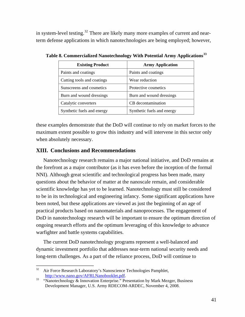
in system-level testing.32 There are likely many more examples of current and near-term defense applications in which nanotechnologies are being employed; however,
Table 8. Commercialized Nanotechnology With Potential Army Applications33
Existing Product Army Application
Paints and coatings Paints and coatings
Cutting tools and coatings Wear reduction
Sunscreens and cosmetics Protective cosmetics
Burn and wound dressings Burn and wound dressings
Catalytic converters CB decontamination
Synthetic fuels and energy Synthetic fuels and energy these examples demonstrate that the DoD will continue to rely on market forces to the maximum extent possible to grow this industry and will intervene in this sector only when absolutely necessary.
XIII. Conclusions and Recommendations
Nanotechnology research remains a major national initiative, and DoD remains at the forefront as a major contributor (as it has even before the inception of the formal NNI). Although great scientific and technological progress has been made, many questions about the behavior of matter at the nanoscale remain, and considerable scientific knowledge has yet to be learned. Nanotechnology must still be considered to be in its technological and engineering infancy. Some significant applications have been noted, but these applications are viewed as just the beginning of an age of practical products based on nanomaterials and nanoprocesses. The engagement of DoD in nanotechnology research will be important to ensure the optimum direction of ongoing research efforts and the optimum leveraging of this knowledge to advance warfighter and battle systems capabilities.
The current DoD nanotechnology programs represent a well-balanced and dynamic investment portfolio that addresses near-term national security needs and long-term challenges. As a part of the reliance process, DoD will continue to
32 Air Force Research Laboratory’s Nanoscience Technologies Pamphlet,
http://www.nano.gov/AFRLNanobooklet.pdf. 33 “Nanotechnology & Innovation Enterprise.” Presentation by Mark Mezger, Business
Development Manager, U.S. Army RDECOM-ARDEC, November 4, 2008.
41
coordinate its nanotechnology programs amongst the Services, DARPA, and other federal agencies to maximize leveraging and avoid duplication and redundancy. The DoD continues to view nanotechnology as one of the enabling technologies that should receive the highest level of corporate attention and coordination as described in the 2007 Department of Defense Research and Engineering Strategy.34 DoD 2010 plans include continuing, approximately stable support for the PCAs associated with the DoD mission. The primary PCAs will remain Fundamental Nanoscale Phenomena and Processes, Nanoscale Devices and Systems, and Nanomaterials. New projects in nanotechnology, as in all thematic areas, are awarded on a competitive basis, so the actual balance of investment may vary somewhat from current expectations.
As basic research efforts in nanotechnology continue to mature, it is anticipated that the results will be transitioned to applied research efforts and advanced technology development in both the military and industry sectors. We have seen this trend since the 2007 report, and some concrete examples have been documented in this report. Increasing emphasis is being put on communication and effective transitioning of research to technology development with and among the military departments and agencies. Furthermore, DoD is continuing to work with the NSTC Interagency Working Group to augment the federal program in nanomanufacturing, since this area remains a significant barrier to the commercialization of nanomaterials and nanotechnology-based products.
Current R&D programs in support of nanotechnology span a broad range of S&T areas that are of primary interest to DoD. Because these programs are inherently high risk with the potential for extremely high payoff, major advances in the application of nanotechnology to the military are often unpredictable (particularly when attempting to assess basic research and early applied research efforts). For this reason, a stable (relative to the overall DoD R&D budget) and strategic (relative to the worldwide investment) nanotechnology R&D investment portfolio has to be maintained to identify and capture the critical technological breakthroughs needed to provide revolutionary advantages for warfighter and battle systems capabilities. Breakthroughs in nanotechnology have to be exploited for these capabilities, but DoD’s support for highly adaptive and innovative R&D (which helped conceive the current international nanotechnology focus) cannot be restricted by a singular focus on nanotechnology or any other single area.
34 http://www.dod.mil/ddre/doc/Strategic_Plan_Final.pdf.
42

The DoD program in nanotechnology remains robust and well balanced and is expected to continue as an important investment area based upon its scientific competitiveness and applicative potential for enhancing Defense capabilities.
43
List of Acronyms
2D two-dimensional 3D three-dimensional AFOSR Air Force Office of Scientific Research AFRL Air Force Research Laboratory ARC Australian Research Council ARDEC Armament Research, Development, and Engineering
Center ARL Army Research Laboratory ARO Army Research Office ASCI application-specific integrated circuit BICAMN Bar Ilan Center for Advanced Materials and
Nanotechnology BMBF Bundesministerium für Bildung und Forschung (The
Federal Ministry of Education and Research) BMVg Bundesministerium der Verteidigung (The Federal
Ministry of Defence) CB Chem-Bio CBDP Chemical and Biological Defense Program CBR chemical, biological, and radiological CERA Carbon Electronics for Radio Frequency Applications CSIR Council of Scientific and Industrial Research DARPA Defense Advanced Research Projects Agency DBRAG Defense Basic Research Advisory Group DDR&E Director, Defense Research and Engineering DE directed energy DIB Defense Industrial Base DIPAS Defense Institute for Physiology and Allied Sciences DLJ Defense Laboratory Jodhpur DMRL Defense Metallurgical Research Laboratory DMSRDE Defense Materials and Stores Research and Development
Establishment DNA deoxyribonucleic acid DoD Department of Defense DoDD Department of Defense Directive DOE Department of Energy DRDO Defence Research and Development Organisation DSTAG Defense Science and Technology Group DSTO Defence Science and Technology Organisation DTRA Defense Threat Reduction Agency ESOH Environment, Safety, and Occupational Health
44
EU European Union FET field-effect transistor GNIC Gwangju Nanotechnology Integration Center GPS Global Positioning System HPM high power microwave IC integrated circuit InAs indium arsenide INI Iranian Nanotechnology Initiative INNI Israel National Nanotechnology Initiative InP indium phosphide IPT Integrated Product Team IR infrared ITRI Industrial Technology Research Institute KAIST Korea Advanced Institute of Science and Technology KANC Korea Advanced Nano Fab Center LED light emitting diode LWIR long wave infrared MEMS microelectromechanical systems METI Ministry of Economy, Trade, and Industry MEXT Ministry of Education, Culture, Sports, Science and
Technology MITI Ministry of International Trade and Industry MoST Ministry of Science and Technology MRE meal, ready-to-eat MURI Multidisciplinary University Research Initiative MWIR medium wave infrared nano-PCR nanoscale polymerase chain reaction NANOTECH National Nanotechnology Center NASA National Aeronautics and Space Administration NCNT National Center for Nanomaterials Technology NEDO New Energy and Industrial Technology Development
Organization NEMS nanoelectromechanical systems NIH National Institutes of Health NIST National Institute of Standards and Technology NNCO National Nanotechnology Coordination Office NNFC National NanoFab Center NNI National Nanotechnology Initiative NNIC National Nanotechnology Integration Center NPAC Nano Practical Application Center NRL Naval Research Laboratory NSET Nanoscale Science and Engineering Technology NSF National Science Foundation
45
46
NSRRC National Synchrotron Radiation Research Center NSTDA National Science and Technology Development Agency OEM original equipment manufacturer ONR Office of Naval Research PCA Program Component Area POSS polyhedral oligomeric silsesquioxanes PRC Peoples Republic of China PtSi platinum-silicide R&D research and development RBNI Russell Berrie Nanotechnology Institute RDECOM Research, Development, and Engineering Command RF radio frequency RHPB Applied Biotechnology Branch (of AFRL) S&T science and technology SBIR Small Business Innovation Research SEM scanning electron microscopy Si silicon SiC silicon carbide SRNL Savannah River National Laboratory STTR Small Business Technology Transfer THB Thai Baht TIC toxic industrial chemical TRL Technology Readiness Level U.S.C. United States Code UAV unmanned air vehicle USD U.S. dollars