Embed Size (px)
Citation preview
DEFECTS AND DISORDER IN CARBON NANOTUBES
Philip G. Collins University of California at Irvine, Irvine, USA
1. INTRODUCTION AND OUTLINE
The presence of defects subtly alters all of a material’s properties. Chemical reactivity, mechanical strength, optical absorption, and electronic transport all vary with defect concentration. Despite these wide-ranging effects, however, it is very rare for defect control to be critical to a particular application. For example, electronic circuits perform perfectly well in the presence of defects. Even though a defect might trap or scatter charge carriers, a typical conductor will electrostatically screen such sites and still maintain a preponderance of unaffected carriers and conduction channels.
In reduced dimensions these generalizations begin to fail. In one-dimensional (1-D) systems, defects play the most significant roles, and they can dominate physical property measurements. For example, the strength of a 1-D chain cannot exceed its weakest link. Charge carriers in 1-D are confined to a single trajectory and cannot avoid a scattering center nor scatter into nearby momentum states. Such consequences are critically important to the newly developing field of nanoscience, in which low dimensional materials are synthesized, characterized, and integrated into applications.
_________________________
To appear in Oxford Handbook of Nanoscience and Technology: Frontiers and Advances. A.V. Narlikar, & Y.Y. Fu, Eds. (Oxford Univ. Press, Oxford, 2009).
Carbon nanotubes (CNTs) represent an ideal materials system for studying and probing the possible effects of defects. CNTs, and single-walled nanotubes in particular, are nearly 1-D materials exhibiting a wide range of interesting physical behaviors. Enormous progress has been made over the last decade characterizing and studying this material system, to the point that the strength, chemical activity, and electrical resistivity of individual CNTs have all been intensively investigated. However, despite the progress in CNT research generally, CNTs with point defects represent a rich and mostly untapped system. Experimental investigations have only begun to address the loss of mechanical strength, the change in optical activity, or the increase in electrical resistance that can be attributed to point defects. At present, no clear consensus has emerged on the properties of CNT defects, nor especially any quantitative correlation between these properties and different defect types. This topic is likely to demand more attention as the field matures away from claims of CNTs as perfect and defect-free materials.
The purpose of this chapter is therefore to provide a practical introduction to the subfield of CNT defects, and to provide the background necessary to begin clarifying the physical consequences of defects, especially wherever these effects can be distinguished from the underlying CNT properties. For this context, it is appropriate to narrowly define CNTs as highly crystalline materials sharing common physical and chemical properties, and to attribute all departures to varying degrees of modification. The most narrow definition of pristine CNTs, to be used throughout this chapter, is of seamless and undistorted graphitic cylinders with aspect ratios exceeding at least 100. Single-walled nanotubes (SWNTs) consist of a single cylinder, and multi-walled nanotubes (MWNTs) have multiple concentric cylinders separated by nearly the same distance as the van der Walls stacking of sheets in graphite. Throughout the chapter, separate abbreviations will be used to distinguish SWNTs from MWNTs, with carbon nanotubes in general being abbreviated as CNTs.
A great deal of theoretical modeling has been completed on the topic of CNT defects, and much of it is reviewed by other chapters in this series. This chapter has a distinctly different purpose. As a practical introduction, this chapter aims to emphasize promising directions and practical techniques, in order to help researchers gauge future directions of the field. The chapter also attempts to focus on the middle ground where experimental and theoretical techniques have tractable overlap, and it is therefore somewhat biased towards SWNTs and single defects or very low defect densities. Despite this focus, many potential CNT applications require high degrees of disorder. For these, extreme oxidation of CNTs is an enabling first step towards interconnecting CNTs with polymers, catalytic particles, biomolecules, or other functional elements to make composite hybrids. Many reviews exist on the chemical methods for further tailoring highly disordered CNTs (Hirsch, 2002; Banerjee et al., 2005; Lu and Chen, 2005).
The organization of the chapter is into three main sections. Section 2 is a pedagogical categorization of the types of defects and disorder found in CNTs. Beginning with lattice vacancies and bond rotations, the discussion progresses through extrinsic disorder and concludes with a brief section on highly disordered CNT materials. Section 3 next describes the most effective experimental methods for locating defects based on their short-range effects. The section focuses on precision techniques useful for individual point defects, but also touches upon lower precision methods suitable for bulk characterization. Section 4 concludes with a review of the long-range consequences that CNT defects have on physical properties. Certain types of defects disproportionately perturb physical properties. Besides being consequential to CNT applications, these types of defects are also the easiest to observe experimentally, making them overrepresented in the field’s current literature. As defects having more subtle effects are observed and characterized, this natural bias will fade.
2. CATEGORIZATION OF DEFECT AND DISORDER
In the period of 1995-96, opinions differed on the crystalline quality of carbon CNTs. Ebbesen declared, “Evidence is accumulating that carbon nanotubes are rarely as perfect as they were once thought to be,” (Ebbesen and Takada, 1995) only a few months apart from the publication of “Crystalline Ropes of Single Walled Nanotubes” (Thess et al., 1996). The second publication, combined with the worldwide sharing of material by R. E. Smalley’s research group, helped to popularize the latter judgment. Over the ensuing decade, the prevailing conception of CNTs and particularly SWNTs continued to be one of perfectly crystalline wires, with every major advance in SWNT synthesis (Thess et al., 1996; Cassell et al., 1999; Nikolaev et al., 1999; Hata et al., 2004) reinforcing this belief through claims of defect-free material.
Of course, it is thermodynamically impossible for defect densities to go to zero, even in highly pure crystalline systems. The ground state of pure carbon systems is the sp2 conjugated lattice of the graphene sheet, but many possible topological perturbations are possible. Defects that are not too energetically costly will exist in equilibrium proportions determined by their Boltzman factor exp(-Ed/kbT). One might imagine that the strong sp2 bonding network of graphitic carbons would energetically preclude defect formation, and in fact atomic vacancies are quite unfavorable. But line and screw defects, interstitials, and bond rotation defects are all observed in graphites in considerable numbers. An extensive literature has developed around defects in graphite, much of which is applicable to newer materials such as graphene and CNTs. Telling and Heggie have recently completed an extensive review of radiation-induced damage in graphites (Telling and Heggie, 2007), a field dating back to the beginnings of the nuclear industry over 50 years ago. Even though this research has focused on high energy processes, it still provides an excellent starting point for understanding CNTs.
Two special differences between graphites and CNTs arise. First, the allowed categories of defects are restricted by dimensionality. SWNTs obviously cannot contain higher dimensional defects like line and screw dislocations. Isolated SWNTs also cannot support many of the common interstitial defects, which are stabilized by inter-sheet bonding in the graphites. On the other hand, the point defects found in graphites are more complicated in CNTs because of circumferential, curvature-induced strain. Since carbon bonds exist at various angles to this strain, defect stabilities depend precisely on position within the lattice, as well as CNT diameter and helicity (Carlsson, 2006).
This Section begins by continuing along these lines, analyzing CNT defects likely to exist in the most pristine materials. Next, the effects of post synthesis processing will be considered, since most mechanical and chemical processing serve to nucleate even more defects. The section concludes by considering two types of disorder that are not lattice defects per se – carbonaceous and noncarbonaceous material in the surrounding environment – but that nonetheless can be nearly indistinguishable from defects in the ways that they perturb CNT properties.
2.1. Intrinsic defects in highly-ordered CNTs
2.1.1 Vacancies
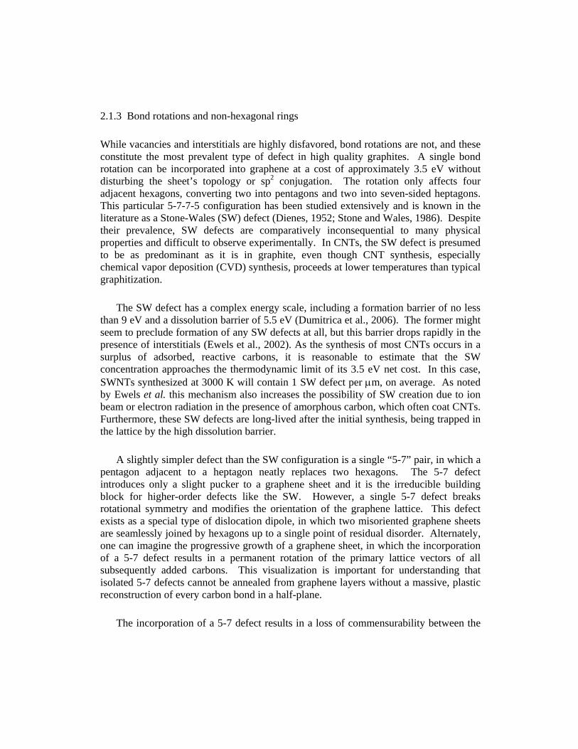
The most typical type of defects in crystalline lattices are point vacancies, interstitials, and bound complexes of the two. A missing or extra atom is a small perturbation in weakly bonded metal crystals, but the same is not true in graphene. A graphene vacancy breaks three short, strong C=C bonds and costs nearly 7.8 eV (Kaxiras and Pandey, 1988). Even though CNT synthesis is a high temperature process (up to 3000 °C), the likelihood of incorporating such sites during crystal growth remains extremely low. Furthermore, the carbon-rich synthetic environment excludes the likelihood of vacancy survival, beyond mere thermodynamic considerations.
Vacancy defects are not uncommon, however, and are produced post-synthesis. For example, knock-on events by high energy electron, ion, or neutron radiation can dislodge or fully remove a carbon atom. This type of vacancy initially results in three dangling bonds that will immediately rehybridize or react with surrounding molecules. One rearrangement amenable to theoretical study is the so-called 5-1DB vacancy defect, in which two of the dangling bonds bridge to form a strained, pentagonal 5-membered ring, leaving only a single dangling bond “1DB” (Ajayan et al., 1998), confirmed by (Lu and Pan, 2004). The resulting structure costs only 5 – 6 eV , though substantial disagreement continues over whether this rearrangement occurs spontaneously and whether it is even the lowest energy configuration (Berber and Oshiyama, 2006).
Further theoretical effort has focused on how the dangling bonds associated with one or more vacancies might serve as sites for interconnecting nanotubes, providing chemical sensitivity, or for incorporating dopants (Liu et al., 2006a; Liu et al., 2006b; Kotakoski et al., 2007).
Considerations of dangling bonds are somewhat academic when CNTs are surrounded by a typical experimental environment. Unlike vacancies produced deep in a graphite crystal, CNT surfaces interact with adsorbed gases, moisture, supporting substrates, and nearby amorphous carbons, all of which provide spontaneous reaction pathways to saturate dangling bonds. In all but ultrahigh vacuum conditions, most intermediates are susceptible to nucleophilic attack by H2O, making –OH terminated vacancies one of the most likely, and physically relevant, configurations.
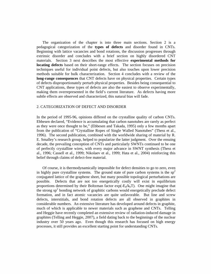
The metastable chemistry of a single vacancy also drives a tendency towards vacancy coalescence. In graphite, a di-vacancy formed by two missing atoms only costs ~1 eV more than the mono-vacancy, and nearly 6 eV less than two separated mono-vacancies. Thus, particularly during annealing processes, single defects are observed to merge and grow into larger voids in graphene sheets. In SWNTs, the vacancy migration barrier is only 1 eV, suggesting mobility at temperatures as low as 100 – 200 °C (Krasheninnikov et al., 2006). The di-vacancy has a few notable properties, including the ability to reconstruct into a pentagon, octagon, and pentagon (5-8-5) structure that is free of dangling bonds. With the additional strain of curvature, di-vacancies in SWNTs are believed to have smaller formation energies than mono-vacancies by nearly 1.5 eV (Krasheninnikov et al., 2006).
Fig. 1: Small vacancy defects in the graphene system. Mono-vacancy (a) before and (b) after reconstruction and H-termination of the remaining dangling bond. Di-vacancy (c) before and (d) after reconstruction.
a) b) c) d)
2.1.2 Interstitials
Interstitials form a second important category of defects generally. An interstitial defect consists of an extra atom not on any lattice site, bonded within an otherwise perfect lattice. Oxygen interstitials, for example, limit the purity and performance of the world’s best silicon crystals. In diamond and graphene, very short lattice bonds prohibit the inclusion of interstitials, and even atomic hydrogen cannot freely diffuse through a graphene sheet. In the case of graphites, however, the interstitial nomenclature is relaxed to include out-of-plane, covalently bonded carbon atoms. Such defects cost nearly 5.5 eV, and they will not be incorporated during CNT synthesis except by arc or laser ablation, where extremely high temperature, carbon-rich plasmas are used. Instead, the primary source of interstitials is likely to again be knock-on damage, since the production of each vacancy also releases a carbon atom. These atoms usually remain confined within a graphite crystal, and they will be accommodated by producing a covalent link across two neighboring graphene sheets. This type of interstitial, driven by aromaticity and low coordination, will migrate within and between graphene layers and until it binds to a vacancy site to produce a stable, vacancy-interstitial complex called a Frenkel defect.
In CNTs, the carbons freed by knock-on damage are not so well trapped, particularly when the material is SWNTs diluted for imaging purposes. Furthermore, carbons on surfaces remain highly mobile, since they cannot be stabilized by bonding among two graphene sheets. A carbon bound to a single sheet has a binding energy of 1.2 eV, but a migration energy less than 0.1 eV (Xu et al., 1993; Nordlund et al., 1996). Thus, an interstitial is highly mobile and, since the barrier to Frenkle recombination is only 0.2 eV, these defects are likely to be short-lived in CNTs (Telling and Heggie, 2007). If they do not recombine, candidate interstitials probably agglomerate or bind with adsorbates to form small, physisorbed clusters of graphitic or amorphous carbon. Thus Frenkel defects, like vacancies, are not likely to play large roles in the properties of CNTs experimentally.
When discussing CNTs, it is important to distinguish between interstitials, adducts, adsorbates, and intercalants. As defined here, CNT interstitials are atomic carbons covalently bonded between two carbon shells and, rarely, to just one. Covalent attachments by other atoms or molecules are termed adducts and treated below in Section 2.3. Chemisorbates and physisorbates are more weakly bound than adducts, comprising a loosely-defined continuum of binding strengths associated with different degrees of charge transfer to the CNT surface. When these adsorbates sit between two or more layers of graphene, they are termed intercalants. The intentional intercalation of graphite crystals has an extensive history (Enoki et al., 2003), since it provides a means to tailor graphite’s physical properties. In CNTs, such intercalants are described as a source of extrinsic disorder in Section 2.2.
2.1.3 Bond rotations and non-hexagonal rings
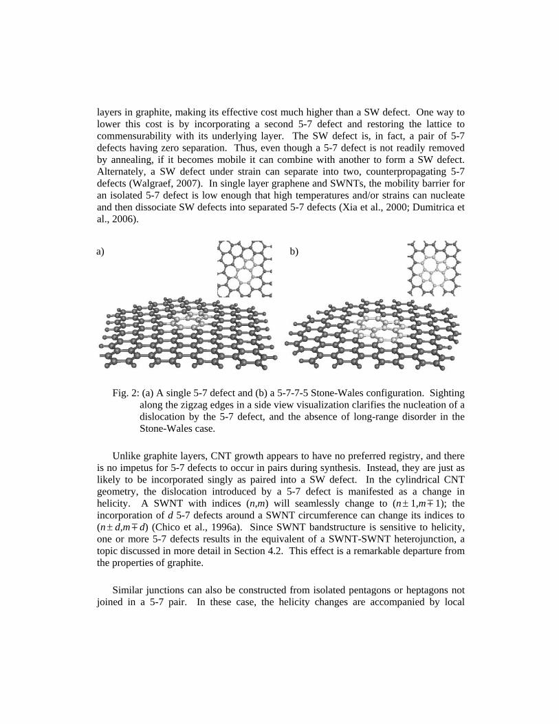
While vacancies and interstitials are highly disfavored, bond rotations are not, and these constitute the most prevalent type of defect in high quality graphites. A single bond rotation can be incorporated into graphene at a cost of approximately 3.5 eV without disturbing the sheet’s topology or sp2 conjugation. The rotation only affects four adjacent hexagons, converting two into pentagons and two into seven-sided heptagons. This particular 5-7-7-5 configuration has been studied extensively and is known in the literature as a Stone-Wales (SW) defect (Dienes, 1952; Stone and Wales, 1986). Despite their prevalence, SW defects are comparatively inconsequential to many physical properties and difficult to observe experimentally. In CNTs, the SW defect is presumed to be as predominant as it is in graphite, even though CNT synthesis, especially chemical vapor deposition (CVD) synthesis, proceeds at lower temperatures than typical graphitization.
The SW defect has a complex energy scale, including a formation barrier of no less than 9 eV and a dissolution barrier of 5.5 eV (Dumitrica et al., 2006). The former might seem to preclude formation of any SW defects at all, but this barrier drops rapidly in the presence of interstitials (Ewels et al., 2002). As the synthesis of most CNTs occurs in a surplus of adsorbed, reactive carbons, it is reasonable to estimate that the SW concentration approaches the thermodynamic limit of its 3.5 eV net cost. In this case, SWNTs synthesized at 3000 K will contain 1 SW defect per μm, on average. As noted by Ewels et al. this mechanism also increases the possibility of SW creation due to ion beam or electron radiation in the presence of amorphous carbon, which often coat CNTs. Furthermore, these SW defects are long-lived after the initial synthesis, being trapped in the lattice by the high dissolution barrier.
A slightly simpler defect than the SW configuration is a single “5-7” pair, in which a pentagon adjacent to a heptagon neatly replaces two hexagons. The 5-7 defect introduces only a slight pucker to a graphene sheet and it is the irreducible building block for higher-order defects like the SW. However, a single 5-7 defect breaks rotational symmetry and modifies the orientation of the graphene lattice. This defect exists as a special type of dislocation dipole, in which two misoriented graphene sheets are seamlessly joined by hexagons up to a single point of residual disorder. Alternately, one can imagine the progressive growth of a graphene sheet, in which the incorporation of a 5-7 defect results in a permanent rotation of the primary lattice vectors of all subsequently added carbons. This visualization is important for understanding that isolated 5-7 defects cannot be annealed from graphene layers without a massive, plastic reconstruction of every carbon bond in a half-plane.
The incorporation of a 5-7 defect results in a loss of commensurability between the
layers in graphite, making its effective cost much higher than a SW defect. One way to lower this cost is by incorporating a second 5-7 defect and restoring the lattice to commensurability with its underlying layer. The SW defect is, in fact, a pair of 5-7 defects having zero separation. Thus, even though a 5-7 defect is not readily removed by annealing, if it becomes mobile it can combine with another to form a SW defect. Alternately, a SW defect under strain can separate into two, counterpropagating 5-7 defects (Walgraef, 2007). In single layer graphene and SWNTs, the mobility barrier for an isolated 5-7 defect is low enough that high temperatures and/or strains can nucleate and then dissociate SW defects into separated 5-7 defects (Xia et al., 2000; Dumitrica et al., 2006).
Fig. 2: (a) A single 5-7 defect and (b) a 5-7-7-5 Stone-Wales configuration. Sighting along the zigzag edges in a side view visualization clarifies the nucleation of a dislocation by the 5-7 defect, and the absence of long-range disorder in the Stone-Wales case.
Unlike graphite layers, CNT growth appears to have no preferred registry, and there is no impetus for 5-7 defects to occur in pairs during synthesis. Instead, they are just as likely to be incorporated singly as paired into a SW defect. In the cylindrical CNT geometry, the dislocation introduced by a 5-7 defect is manifested as a change in helicity. A SWNT with indices (n,m) will seamlessly change to (n± 1,mm 1); the incorporation of d 5-7 defects around a SWNT circumference can change its indices to (n± d,mm d) (Chico et al., 1996a). Since SWNT bandstructure is sensitive to helicity, one or more 5-7 defects results in the equivalent of a SWNT-SWNT heterojunction, a topic discussed in more detail in Section 4.2. This effect is a remarkable departure from the properties of graphite.
Similar junctions can also be constructed from isolated pentagons or heptagons not joined in a 5-7 pair. In these case, the helicity changes are accompanied by local
a) b)
concave or convex distortions to the SWNT sidewall. The additional curvature is allowed in SWNT and fullerene topologies, but forbidden in planar graphite, making these types of defects a category wholly unique to CNTs. The addition of heptagons around a SWNT circumference will cause the diameter to flare out, and with an equal number of pentagons the distortion can be seamlessly joined to a larger diameter SWNT, and in fact these were the very first properties of CNTs ever studied (Iijima et al., 1992b). In general, equal numbers of pentagons and heptagons allow extended structures where both chirality and diameter may vary, though some chiralities may only be joined with accompanying kinks or bends.
An elegant demonstration of this effect has been reported by Yao et al. (Yao et al., 2007). The synthesis of different SWNT diameters is partly determined by growth temperature (Bandow et al., 1998), and by changing temperature midgrowth one can move the optimum diameter from one value to another. Yao et al. nucleated SWNTs in one diameter range and then changed the growth temperature, making a different size more preferable for continued growth. The SWNTs responded by changing diameter through the incorporation of 5-7 defects (Yao et al., 2007). The technique promises to improve the intentional creation of SWNT heterojunctions for further investigation.
2.1.4 Summary and caveat
In summary, the types of defects intrinsic to CNTs provide some interesting surprises. The most conventional types of defects, like vacancies and interstitials, are unlikely to be found in pristine CNTs. The Stone-Wales 5-7-7-5 configuration unique to graphitic systems is predicted to be a relatively common type of defect. Equally likely are various topology-changing combinations of 5-7 pairs, including physically separated pentagons and heptagons that are uniquely stable in CNTs. These latter defects can have significant, long-range consequences.
Table 1 below summarizes estimated defect energies Ed of each defect type and provides an estimate for the expected equilibrium concentration of each at two common CNT synthesis temperatures. Small SWNTs contain roughly 106 carbons per micrometer of length, so that even the most common types of defects have mean separations of 1 μm. Note that predicted values of Ed vary widely in the literature and, particularly in CNTs, are not readily accessible experimentally. The equilibrium concentrations in Table 1 set lower limits on experimental defect concentrations, and are in reasonably good agreement with some highly crystalline SWNTs. Many experiments, however, observe much higher defect concentrations. Carlsson has suggested that heats of formation, which are smaller than the Ed values, might provide concentrations in better agreement with experiment (Carlsson, 2006). As described in the following parts of Section 2, however, many additional sources of defects and disorder also contribute.
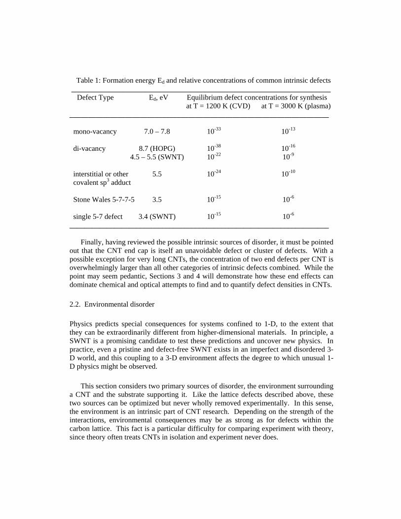
Table 1: Formation energy Ed and relative concentrations of common intrinsic defects ______________________________________________________________________ Defect Type Ed, eV Equilibrium defect concentrations for synthesis at T = 1200 K (CVD) at T = 3000 K (plasma) ______________________________________________________________________ mono-vacancy 7.0 – 7.8 10-33 10-13
di-vacancy 8.7 (HOPG) 10-38 10-16 4.5 – 5.5 (SWNT) 10-22 10-9 interstitial or other 5.5 10-24 10-10 covalent sp3 adduct Stone Wales 5-7-7-5 3.5 10-15 10-6 single 5-7 defect 3.4 (SWNT) 10-15 10-6 ______________________________________________________________________
Finally, having reviewed the possible intrinsic sources of disorder, it must be pointed out that the CNT end cap is itself an unavoidable defect or cluster of defects. With a possible exception for very long CNTs, the concentration of two end defects per CNT is overwhelmingly larger than all other categories of intrinsic defects combined. While the point may seem pedantic, Sections 3 and 4 will demonstrate how these end effects can dominate chemical and optical attempts to find and to quantify defect densities in CNTs.
2.2. Environmental disorder
Physics predicts special consequences for systems confined to 1-D, to the extent that they can be extraordinarily different from higher-dimensional materials. In principle, a SWNT is a promising candidate to test these predictions and uncover new physics. In practice, even a pristine and defect-free SWNT exists in an imperfect and disordered 3-D world, and this coupling to a 3-D environment affects the degree to which unusual 1-D physics might be observed.
This section considers two primary sources of disorder, the environment surrounding a CNT and the substrate supporting it. Like the lattice defects described above, these two sources can be optimized but never wholly removed experimentally. In this sense, the environment is an intrinsic part of CNT research. Depending on the strength of the interactions, environmental consequences may be as strong as for defects within the carbon lattice. This fact is a particular difficulty for comparing experiment with theory, since theory often treats CNTs in isolation and experiment never does.
2.2.1 Weakly bound adsorbates
The graphite surface is a relatively inert and clean one, and freshly-cleaved graphites were a favorite substrate for early scanning tunneling microscopy work because of its ease of preparation. The graphite surface is hydrophobic, and it is not susceptible to appreciable charge transfer from most adsorbates.
Nevertheless, it would be incorrect to conclude that CNTs in ambient are clean or adsorbate-free. Even hydrophobic surfaces can have adsorbed monolayers of H2O on them. Soluble airborne gases and contaminants, including alkali salts and light hydrocarbons, will also adsorb onto these surfaces. These mobile, low atomic number species are difficult to image by either TEM or STM, and practitioners of these techniques understand that “clean-looking” images do not always capture the real extent of surface chemical disorder.
Three differences between CNTs and graphite suggest ways that CNTs are even more sensitive to adsorbates than graphite surfaces are. First, the CNT curvature results in partial sp3 hybridization, accentuated in small SWNTs, that enhances the π electron density on the cylinder’s outer surface. Common dissolved species like Na+ and H+ will dynamically interact with this surface electron density, even in the absence of chemical bonding or static charge transfer (Kuhn and Silversmith, 1971; Bradley et al., 2003). As recently demonstrated electrochemically, these effects are strong enough to turn the insulating surface of a diamond into a conductor (Chakrapani et al., 2007). Second, curvature also frustrates dense packing of CNTs. Whether bundled together, settled onto a surface, or packed into a pellet, CNT materials have enhanced specific surface areas comprised of physically interconnected, interstitial voids. Adsorbates in these voids can be better coordinated than on flat graphene surfaces, and the voids readily accommodate a wider range of molecular shapes and sizes than do interlayer graphite interstices (Stan and Cole, 1998; Eswaramoorthy et al., 1999; Cole and Hernandez, 2007). Thus, even though a graphite crystal is not intercalated by air or moisture at room temperature, the interstitial pockets between SWNTs must be considered filled unless specifically degassed. Finally, every atom in a hollow SWNT is a surface atom, and the addition of adsorbates is a proportionally larger perturbation in SWNTs than in solid materials. The system can no longer be considered a simple carbon lattice if it is, in fact, a carbon lattice interacting with H-bonded water dipoles, chemisorbed O2
-, or physisorbed hydrocarbons. In the context of novel, low-dimensional physics, the effects of these adsorbates can be enormous because they break the remaining rotational and translational symmetries of a SWNT and physically extend the system away from an idealized, 1-D line.
Placing CNTs into vacuum is insufficient to remove these adsorbates, in the same
way that it does not remove chemisorbed molecules from the internal surfaces of a vacuum apparatus. Extended baking in ultrahigh vacuum, combined with annealing or surface milling, are the standard surface science techniques for preparing atomically clean crystal surfaces. SWNTs are compatible with high temperature vacuum degassing, and a small number of experiments have observed substantial electronic effects from even mild treatments (Collins et al., 2000a; Bradley et al., 2000; Sumanasekera et al., 2000; Derycke et al., 2002; Kim et al., 2003b; Kruger et al., 2003; Kingrey et al., 2006). This literature indicates the need to consider environmental disorder when interpreting CNT results, and similar effects may be equally important for ongoing graphene research (Ishigami et al., 2007; Moser et al., 2008).
Rather than trying to achieve perfect vacuum, a second method of eliminating environmental disorder is to encapsulate CNTs into a homogeneous and uniform chemical environment. A breakthrough in the field of CNT optical spectroscopy occurred when SWNTs were solubilized by hydrophobic surfactants and effectively separated into isolated, uniform micelles (O'Connell et al., 2002; Bachilo et al., 2002). Cocooned into individualized, highly uniform pockets, SWNTs finally began to exhibit spectroscopic fingerprints associated with their different electronic structures, fingerprints that had been quenched or otherwise hidden in previous measurements. Subsequent work, however, has proven that these encapsulating environments must be included in the modeling and interpretation of optical data (Lefebvre et al., 2008). And while encapsulation or vacuum processing can minimize the effects of environmental disorder, they do not remove other common forms of disorder such as amorphous carbon adsorbates or the substrate effects described below.
2.2.2 Substrate effects
As a component of the surrounding environment, substrates deserve special consideration as a source of strong perturbations. A substrate has a different bulk chemistry, electron affinity, and work function than a SWNT, and furthermore will have its own surface electronic structure and morphology. Substrate-SWNT interactions can have multiple unintended physical and chemical consequences, only one of which is to help trap the adsorbates described above.
For example, CNT devices are often fabricated by placing CNTs on a dielectric or on a thin oxide grown on a semiconductor. For electrical measurements, this CNT-oxide-semiconductor architecture allows electrostatic coupling between a semiconducting CNT and an underlying electrode to vary the CNT Fermi level and produce transistor-like switching (Biercuk et al., 2008). This same coupling, however, is decidedly 3-D. The dielectric properties of the substrate screen a portion of the long-range, electron-electron interactions that are predicted to cause special, non-Fermi liquid
behaviors in 1-D conductors (Kane et al., 1997). If a 1-D conductor strongly coupled to electrodes is a 3-D system, then it is well suited to substrate-bound applications like electronics but no longer a prime candidate for probing novel physics. Furthermore, even traditional applications like transistors cannot take full advantage of CNTs without special care. Modeling of “needle contact,” quasi-1-D electrodes suggests that order-of-magnitude performance improvements remain to be observed if CNT dimensionality can be more effectively managed and integrated into appropriate architectures (Heinze et al., 2005).
Besides electrostatic gating, the principal CNT-substrate interaction is generally attributed to be van der Waals adhesion. This adhesion, which is insensitive to lattice mismatch with the SWNTs, is strong enough to quench long-wavelength SWNT phonons like twistons and keep SWNTs securely attached to surfaces. However, the premise that SWNTs are largely inert and only weakly adsorbed by substrates is open to ongoing research. Modeling and experiment both suggest that more complex electronic rehybridization occurs spontaneously, even on relatively stable substrates such as SiO2 (Czerw et al., 2002; Maiti and Ricca, 2004; Tsetseris and Pantelides, 2006). This type of rehybridization is driven in part by CNT strain, and therefore is a diameter-dependent effect. Another strong effect occurs at the interfaces between small SWNTs and metals. Metal coatings on SWNTs can very effectively shunt the SWNT’s 1-D electrical conductivity, invalidating the normal experimental technique of 4-point resistance measurements (Bezryadin et al., 1998). These effects may also explain the diameter dependent, interfacial resistance between metallic SWNTs and metal electrodes, which complicate measurements of ballistic conductance in small diameter SWNTs (Kim et al., 2005; Heinze et al., 2005). Thermal conductivity indicates similar effects on insulating substrates. Freely suspended, current carrying CNTs will self heat to the point of oxidation, but on substrates decidedly different characteristics are observed (Yao et al., 2000; Collins et al., 2001; Pop et al., 2006). In fact, thermal emission microscopy is unable to measure any temperature rise in the latter case, suggesting that heat is very effectively transported out of the carbon lattice by strong substrate interactions. In summary, a number of consequential effects occur when CNTs sit on substrate surfaces, even chemically inert ones.
In addition to these general surface interactions, CNTs have enhanced coupling to a substrate when defects are present. Defects in a CNT will bind covalently to many substrates (Krasheninnikov et al., 2002a; Kotakoski and Nordlund, 2006), complicating the interpretation of their effects. And even if the CNTs are defect-free, defects in the substrate will interact with the CNT. Noncrystalline substrates like thermally grown SiO2 have extensive defect populations that are nearly continuous in energy, and even defects buried below the surface will interact dynamically with surface atoms, with surface adsorbates, and with a CNT’s conduction electrons (Freitag et al., 2007). When cooled to cryogenic temperatures, this substrate disorder becomes static and its

modulation of the CNT potential can be directly imaged (Woodside and McEuen, 2002; Tans and Dekker, 2000). At room temperature, these defects dynamically couple to many degrees of freedom and can participate in inelastic, dissipative scattering, even though lattice defects are typically only considered sources of elastic scattering. For example, defects that are energetically close to the Fermi level dynamically capture and release free carriers from the CNT. This charge trapping and the electronic noise associated with it is a primary engineering challenge of oxide-semiconductor interfaces, and the problem is aggravated in CNTs by their small carrier numbers (Collins et al., 2000b; Lin et al., 2007).
Substrate defects that are energetically deep and/or physically distant are nominally inconsequential to CNTs. Their long-range, perturbing potentials only minimally contribute to sensitive measures such as electron backscattering (McEuen et al., 1999; Ando, 2005). However, this generalization changes when large electric fields are present from to gate biasing voltages. When gated, the small diameter of a CNT produces excessive electric fields that can initiate chemical redox processes in surface contaminants and cause field emission into and out of deep oxide traps (Fuhrer et al., 2002; Radosavljevic et al., 2002). Under these conditions, these defects can become strongly interacting perturbations resulting in memory effects and hysteresis (Kim et al., 2003b; Bradley et al., 2003; Gruneis et al., 2007), distinct from the charge trapping noise described above. Furthermore, substrate defects and chemical variability may play a primary role in some cases of CNT chemoresistance, an actively investigated area that is poorly understood at present (see Section 4.2).
Thus, substrate defects both near to and far from the Fermi level interact with CNTs and give rise to distinguishable dynamical properties. By performing measurements on isolated, freely suspended CNTs, the research community continues working to differentiate between the properties of CNTs and CNT-substrate interactions. However, the appreciation of these interactions is relatively recent, and the literature broadly attributes properties to CNTs that may be specific to suspended SWNTs (Mann et al., 2007; Cao et al., 2005) or suspended MWNTs (Frank et al., 1998; Poncharal et al., 2002). A similar process is repeating itself in the current area of graphene research, though at much greater speed. In 2008, a rapidly growing consensus is developing that bi-layer graphene may be uniformly superior to single-layer graphene because of the consequences on the initial layer of substrate disorder (Lin and Avouris, 2008).
So far, Section 2 has treated two types of disorder that are intrinsic to performing measurements on CNTs. Next, this Section considers extrinsic variables that vary more widely from sample to sample and from technique to technique.
2.3. Disorder introduced by processing
Once synthesized, the manipulation of CNTs into a useful state can involve extensive mechanical and chemical processing. This processing changes the CNT surface and often creates new defect sites. Any meaningful evaluation of defects and their consequences must be in the context of processing history and, consequently, of the targeted application. For example, an isolated, mm-long SWNT is ideal for building multicomponent circuits because it is likely to have long, defect-free regions; the chemist, on the other hand, might prefer the same SWNT chopped into short segments and solubilized. This section addresses some of the most common processing techniques, including the intentional production of new types of defects. Park et al. provide a more extensive review of purification techniques (Park et al., 2006).
First, though, there is one type of processing that tends to improve CNT crystallinity. Vacuum heating anneals CNTs effectively at 1200–1500 °C, even though bulk graphitization of carbons requires temperatures exceeding 2200 °C. The temperature difference is related to the high degree of crystallinity pre-existing in most CNTs. Virtually all oxygen-containing functionalities can be desorbed from a CNT lattice by 1000 °C, and remaining defects and vacancies become mobile by 1200 °C. Above this temperature, 5-7 defects can migrate and annihiliate, and monovacancies left by desorption of carboxylic groups can be healed (Krasheninnikov and Nordlund, 2002; Krasheninnikov et al., 2006). An elegant demonstration of the opening and closing of sidewall vacancies was performed using SWNTs decorated with C60 molecules. Under TEM observation, molecules were observed moving in and out of sidewall holes in individual SWNTs (Smith et al., 1998; Monthioux et al., 2001). At still higher temperatures, a structural relaxation can occur in which pairs of SWNTs merge into larger diameter tubes (Terrones et al., 2000; Terrones et al., 2002a). Of course, vacuum annealing tends to bring the material into thermodynamic equilibrium, meaning that the density of SW defects will typically be reduced, but not to zero.
2.3.1 Purification
The least damaging purification technique employs filtration to separate CNTs from carbon and metal contaminants. Fullerenes and carbon onions, metal clusters, and polyaromatic carbons all readily wash through fine microfilters whereas high aspect ratio CNTs generally do not. Consequently, a relative pure “buckypaper” of CNTs can be formed on such filters, dried into a freestanding film, and further studied (Bandow et al., 1997; Bonard et al., 1997; Eisebitt et al., 1998). The filtering process, while relatively gentle, involves viscous and capillary forces at the nanoscale that generate not only mechanical entanglements but also highly strained kinks and bends. The SW defect is believed to be the primary mechanism for plastic strain release in these

conditions (Nardelli et al., 1998), and the further accumulation of such defects ultimately ruptures the carbon lattice and produces reactive multi-vacancies. In experimental studies, a relatively high resilience and resistance to damage is observed in SWNT bundles and MWNTs, which benefit from multiple parallel shells that enhance rigidity (Falvo et al., 1997).
A harsher purification scheme involves oxidation in air at temperatures of 400 – 750 °C. At the low end of this temperature range, amorphous carbons rapidly convert to CO2 through cooperative reactions with oxygen and water vapor. Graphitic carbons burn more slowly, since in these only the carbon edges are reactive. Often, bulk CNT material contains a significant fraction of graphitic impurities in the form of spherical onions, mesoscopic graphitic flakes and scrolls, and incomplete carbon shells. These carbons will oxidize slowly along their perimeter edges, just like graphite does. Therefore, it is difficult to remove them selectively from CNTs, since they burn at roughly the same rates that CNT endcaps are opened and the CNTs shortened (Ajayan et al., 1993; Ebbesen et al., 1994). In some cases of purification, it is acceptable to lose a significant fraction of the CNTs from a sample in order to fully remove these graphitic impurities. For example, shortening and thinning MWNTs can uncover inner MWNT cylinders that are highly crystalline. In these cases, partial oxidations in wet air may be run at 750 °C (Hiura et al., 1995), though a majority of the CNT material is lost at such high temperatures.
Acid oxidation is a more selective technique that removes amorphous carbons, graphitic mesocarbons, and contaminant metals without causing a substantial loss of CNTs. Widely used, commercial SWNTs such as HiPCO are processed in this manner (Rinzler et al., 1998). Investigation of the interaction between graphitic materials and acids has a long history. The strong acids (e.g. HNO3, H2SO4, HClO4, and HPO4) do not continuously etch graphene’s surface and instead covalently add to its edges and basal planes (Kinoshita, 1988). On the CNT sidewall, these covalent adducts constitute a new type of defect quite different from the intrinsic defects described above. The adduct defect occurs when a single carbon atom rehybridizes to an sp3 conjugation, forming a new bond perpindicular to the sp2 plane as illustrated in Fig. 3a. These adducts are not believed to be populated by high temperature CNT growth, because at high temperatures sp3 carbons are less stable than sp2 ones. In fact, diamond-like edges spontaneously graphitize. Given this stability of the graphite lattice, CNT adducts are often metastable, and many adducts are chemically reversible alterations (Boul et al., 1999; Cui et al., 2003). This reversibility has lead to recent investigation producing graphene sheets from from oxidized graphite.
For example, consider the variety of defect configurations depicted in Fig. 3. An initial acid treatment, perhaps with electrochemical assistance, adds conjugate base anions like NO3
- to the sidewall (Fig. 3a). Chemical reduction of the NO3 adduct may
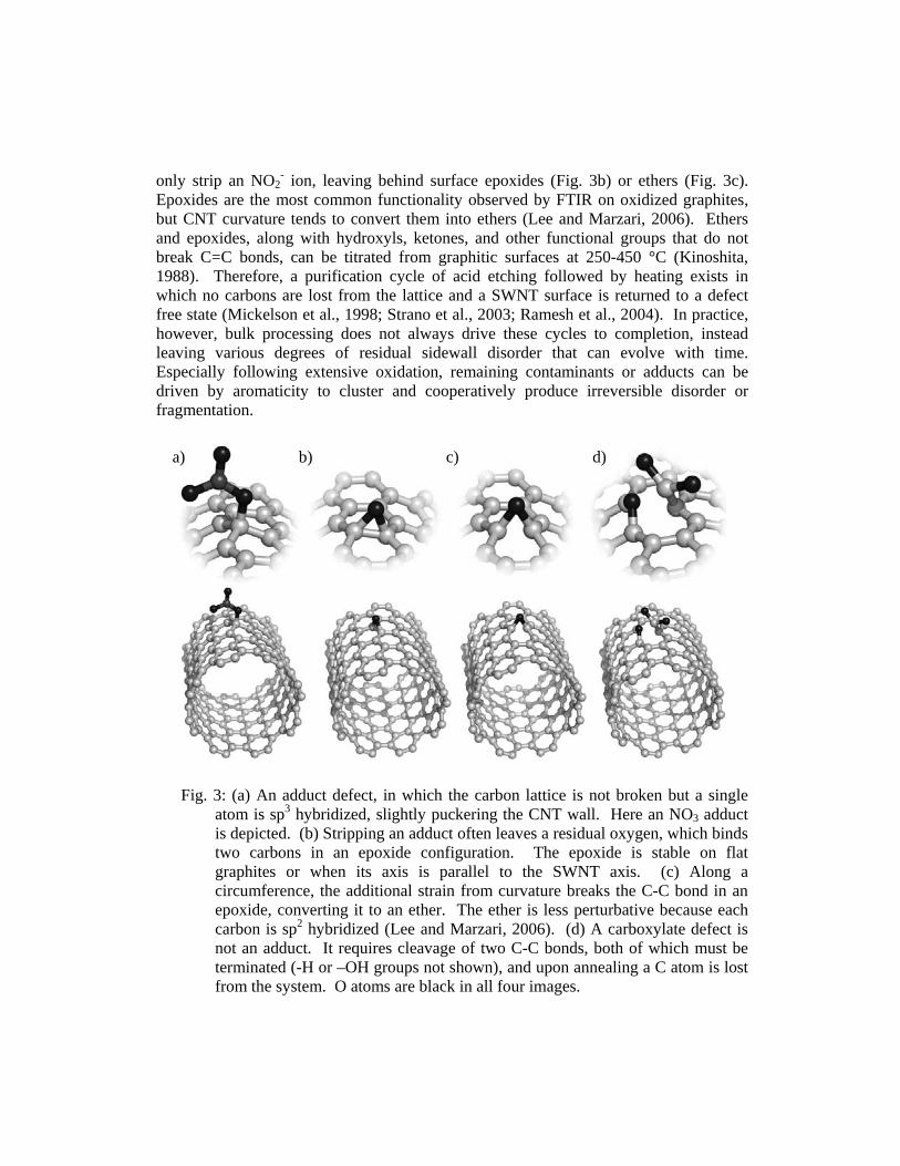
only strip an NO2- ion, leaving behind surface epoxides (Fig. 3b) or ethers (Fig. 3c).
Epoxides are the most common functionality observed by FTIR on oxidized graphites, but CNT curvature tends to convert them into ethers (Lee and Marzari, 2006). Ethers and epoxides, along with hydroxyls, ketones, and other functional groups that do not break C=C bonds, can be titrated from graphitic surfaces at 250-450 °C (Kinoshita, 1988). Therefore, a purification cycle of acid etching followed by heating exists in which no carbons are lost from the lattice and a SWNT surface is returned to a defect free state (Mickelson et al., 1998; Strano et al., 2003; Ramesh et al., 2004). In practice, however, bulk processing does not always drive these cycles to completion, instead leaving various degrees of residual sidewall disorder that can evolve with time. Especially following extensive oxidation, remaining contaminants or adducts can be driven by aromaticity to cluster and cooperatively produce irreversible disorder or fragmentation.
Fig. 3: (a) An adduct defect, in which the carbon lattice is not broken but a single atom is sp3 hybridized, slightly puckering the CNT wall. Here an NO3 adduct is depicted. (b) Stripping an adduct often leaves a residual oxygen, which binds two carbons in an epoxide configuration. The epoxide is stable on flat graphites or when its axis is parallel to the SWNT axis. (c) Along a circumference, the additional strain from curvature breaks the C-C bond in an epoxide, converting it to an ether. The ether is less perturbative because each carbon is sp2 hybridized (Lee and Marzari, 2006). (d) A carboxylate defect is not an adduct. It requires cleavage of two C-C bonds, both of which must be terminated (-H or –OH groups not shown), and upon annealing a C atom is lost from the system. O atoms are black in all four images.
a) b) c) d)
2.3.2 Additional oxidation and functionalization
Chemical processing can be divided into two categories: attempts to purify the CNTs and attempts to modify their surfaces. In the latter, the processing is designed to chemically attack the CNT sidewall, perhaps for the purpose of covalently functionalizing it further. The acid oxidation described above can be used as a starting point for introducing additional disorder, albeit disorder with physical consequences that are different from vacancies or SW defects. Practically, acid treatments are often combined with additional oxidants, heating, and/or ultrasound treatments to produce different stable and permanent functional groups.
A very important such functional group is the carboxylate, a versatile chemical handle for further derivitization (Banerjee et al., 2005) and a starting point for a wide range of research seeking to covalently link CNTs to electrically, optically, or chemically active species. Careful analysis has suggested that even extensive acid oxidation does not generate new carboxylate defects or vacancies in the pristine CNT sidewall (Ziegler et al., 2005a; Ziegler et al., 2005b; Coroneus et al., 2008). This is due, in part, to steric hindrance limiting multiple anions from attacking the same carbon ring. Instead, the further addition of permanganate ions (or, alternatively CrO4
-, OsO4-, or
RuO4-) helps to initiate 2+2 cycloaddition reactions that can break lattice bonds and
produce carboxylates (Hwang, 1995; Biro et al., 2002). This situation is different from the mere addition of a new bond perpendicular to the carbon lattice. The carboxylate defect (Fig. 3d) can result in the removal of carbon atoms from the system and the growth of sidewall holes, making it a much less reversible modification.
The extensive use of such treatments, often combined with heating and ultrasound, is standard processing to separate SWNTs, shorten them into more convenient lengths, and etch away metal and amorphous carbon contaminants (Liu et al., 1998). Typically, the resulting materials are highly defective. Besides having a higher concentration of ends, a preponderance of sidewall hydroxyl- and carboxyl-terminated vacancies are created (Hamon et al., 2001; Mawhinney et al., 2000; Monthioux et al., 2001), and as many as 5% of the C atoms in a SWNT are adjacent to these defects after processing. These heavily modified materials are not the focus of this review; instead, other reviews of SWNT chemistry begin from the premise of high SWNT defect densities (Hirsch, 2002; Banerjee et al., 2005).
2.3.3 Mechanical processing
CNTs are somewhat resistant to mechanical damage from low power ultrasound, and after short processing times no accumulation of damage is typically observable (Furtado et al., 2004). As the processing time increases, however, there is no question that
damage accumulates, and ultimately it can be identified by bulk techniques like optical spectroscopy (Benedict et al., 2005; Grossiord et al., 2007), gas adsorption (Dagaonkar et al., 2002), or others (Satishkumar et al., 1996; Monthioux et al., 2001). The exact resistance to low power ultrasound has not been carefully mapped for individual CNTs, in part because it depends on temperature, solvent, and other factors.
Commercial horn sonicators operate at high powers (e.g. > 15 W) and readily damage CNTs. Bends, buckles, and multivacancies rapidly accumulate with processing time (Lago et al., 1995; Lu et al., 1996), though the effects can be partly mitigated by working in different solvents. Similiary, ball milling is effective at mechanically disintegrating CNTs into onions and amorphous carbons (Li et al., 1999).
Cleverly used, mechanical processing can do more than just destroy CNTs. At the other extreme from ball milling, an AFM tip has been used to “knick” a pristine SWNT and produce a single site of disorder for futher study (Park et al., 2002). One of the most intriguing examples of mechanical processing involved the repeated dipping of a MWNT into a Hg bath (Frank et al., 1998; Poncharal et al., 2002). Over the course of thousands of dipping cycles, visible quantities of amorphous carbons and incomplete graphitic shells were observed sloughing off MWNT bundles onto the Hg surface. Once cleaned in this manner, the MWNTs exhibited ballistic electrical conducances matching theoretical limits.
2.3.4 Other Modifications
While robust, the graphitic carbon lattice is susceptible to damage by many means. In a TEM, knock-on events by high energy electrons rapidly create vacancies and can completely fragment MWNTs (Chopra et al., 1995a). Ion irradiation, too, produces vacancies and reactive sites for energies as low as 50 eV (Nordlund et al., 1996). In a focused ion beam, even low dosage Ga+ irradiation used for imaging will tear holes in carbon sidewalls. When put into an energetic plasma, CNTs are rapidly etched by O2, covalently functionalized by H2 (Buchs et al., 2007), or fragmented by heavy ions. All of these mechanisms are useful for the intentional study of the effects of defects (Osvath et al., 2005; Robinson et al., 2006), and completely misleading when not properly accounted for. The wary experimentalist questions whether each technique in a process is intrusive or perturbative.
For example, CNTs are routinely imaged by SEM and exposed to high electron doses in the electron beam lithography process. Some troubling observations of beam-induced changes have been observed in CNT devices, with the suggestion that few-keV electrons can initiate reactions including sidewall oxidation by water (Suzuki and Kobayashi, 2005; Vijayaraghavan et al., 2005). Analysis suggests that the electronic
effects are due to chemical processes on the SiO2 support, not the CNT itself (Rius et al., 2007), providing a specific example of the substrate effects described in Section 2.2b. In any case, a number of research groups rely wholly on AFM imaging and optical lithography in the fabrication of CNT devices in order to avoid unintentional consequences of electron beams.
2.4. Disorder in CNT materials
A final category of disorder is due to impure or noncrystalline starting material. Unlike the point defects that are thermodynamically intrinsic to CNTs, amorphous carbons and distorted or incomplete graphitic shells are unnecessary but common products of CNT synthesis, especially resulting from efforts to produce CNTs at low temperatures or in bulk. A longstanding problem in CNT synthesis continues to be the quantitative evaluation of purity, either before or after additional purification or processing (Niyogi et al., 2002; Itkis et al., 2005; Park et al., 2006). Beyond the difficulty of determining appropriate measures, however, is the even more difficult problem of specifying a practical definition for CNT disorder. The literature accepts a wide range of carbonaceous cylinders under the term “nanotube,” ranging from centimeter-long, 1 nm diameter single walled cylinders to 200-300 nm diameter cylinders composed of herringbone-stacked graphitic sheets. This span fosters misunderstandings and misappropriations, as properties such as high strength, ballistic transport, and chemical inertness measured on one material certainly do not pass on to others.
Disorder includes a wide range of departures from the perfect cylindrical CNT, with the most common ones described below. Tradeoffs exist between material quality and synthetic cost, and in many cases the presence of disorder can be inconsequential or even beneficial depending on the application. However, better informed decisions require more accurate characterizations of disorder and its specific consequences, and empirical batch-by-batch characterization is currently the only way to qualify CNT materials for particular commercial applications.
2.4.1 Mesoscopic carbon and non-carbon constituents
The disorder that affects the immediate appearance of CNTs in high resolution imaging is mainly due to materials adsorbed on their outside walls or incorporated into the cylindrical hollows. Beyond mere appearances, these contaminants substantially change the chemical and physical properties of bulk material. For example, amorphous carbons are more reactive than pristine CNTs, they have more varied functional groups, and they have different surface areas and adsorption characteristics. The processing described in Section 2.3 attempts to remove most such contaminants, but sustained efforts over the last decade have not yet produced high purity CNT material in bulk. This failure, in
turn, severely limits attempts to apply bulk techniques to the study of defect concentrations and their properties.
Metal contamination of CNTs is a noteworthy problem that continues to plague many types of bulk CNT characterization (Park et al., 2006) and continues to be an area of active research (Xiang et al., 2007; Ding et al., 2006; Jurkschat et al., 2007). Transition metals help catalyze CNT growth and are required in all methods of SWNT growth. Post synthesis, the metals are difficult to remove: they are often encapsulated by many spherical layers of graphitic carbon, and they can be in the form of pure metals, carbides, or oxides. Some metal sits at the tips of SWNTs, or inside the endcaps of MWNTs, where complete removal requires extensive etching of the caps and concurrent sidewall damage. When present, these residual metals modify most observable bulk properties – electrochemical activity, thermal stability, surface area and density, magnetic susceptibility, etc. – even when they are only incorporated at the CNT ends (Itkis et al., 2005).
Mesoscopic graphitic carbons are a second primary contaminant in CNTs. While amorphous carbons and fullerenes are easily removed, graphitic flakes are more difficult to selectively oxidize or dissolve because they have the same chemistry as CNTs. Furthermore, these small flakes include incomplete or damaged cylinders partially wrapping around a CNT, in which case it becomes impossible to distinguish contaminated CNTs from highly defective ones. In general, MWNTs are described as highly crystalline and defect-free when high resolution TEM observes smooth, straight, and continuous inner layers, even though one or more disordered outer layers are also resolved. Mild oxidation of the most reactive carbons can eliminate these mesoscopic graphites, but only with a loss of CNT ends, small diameter SWNTs, and an expansion of point defects into larger sidewall holes (Ajayan et al., 1993; Tsang et al., 1993). An alternate approach is to solubilize and dilute the CNTs, which when fully separated can be fractionated (Arnold et al., 2006). Residual mesoscopic flakes are particularly problematic for optical characterization, because they provide a high density of optically active functional groups that are not necessarily present in the underlying CNTs.
2.4.2 MWNT structural defects
In some ways, MWNTs represent an intermediate material between graphite and SWNTs. Their multilayered structure resembles graphite crystals, and like graphite a MWNT stably supports the type of defect known as an interstitial-vacancy bound pair. On closer inspection, though, MWNTs are more complex than either crystalline graphites or SWNTs, and subtle forms of disorder exist. For example, curvature forces adjacent layers in a MWNT to nearly always be incommensurate, and this intrinsic broken symmetry has various consequences (Roche et al., 2001). Analysis also suggests
that some synthesis techniques produce multilayer scrolls, or MWNTs composed of both scrolls and cylinders, rather than merely the purely cylindrical structure (Zhou et al., 1994; Bursill et al., 1995; Feng et al., 1996).
However, the most important contributions to MWNT disorder are much less subtle. MWNT synthesis occurs under rapid, nonequilibrium growth dynamics. The resulting disorder can include tapering cylinders, variable numbers of carbon layers, and partial interior filling, examples of which are shown in Fig. 4. The cylindrical crystalline structure can also be severely compromised by certain additives. So-called “herringbone” and “bamboo” defects mix the physical properties of in-plane and c-axis graphite by introducing graphitic layers misaligned with the primary MWNT axis. The herringbone structure, depicted in Fig. 4e, consists of stacked layers or conical sections that are tilted with respect to the main axis. Herringbone ordering is a common morphology for carbon fibers and nanohorns (Yudasaka et al., 2008), and materials having this structure may or may not have a hollow interior. Bamboo defects consist of several transverse, internal walls segmenting the interior of a MWNT into independent pods or isolated volumes. Bamboo defects are often quasi-periodic, as shown in Fig. 4f, and by nucleating new shells they maintain roughly constant outer diameters.
2.4.3 Substitutional dopants
The high-strength carbon lattice is not generally susceptible to substitutional doping, and cannot be tailored as widely as most technological semiconductors. Therefore, it is unlikely that substitutional dopants exist inadvertently in CNTs. Nevertheless, both B and N atoms can replace C atoms in the graphite lattice without severely disrupting the bonding network. Substitutional doping of graphites by B or N atoms, as well as BN dimers, has been pursued since the 1960’s (Lowell, 1966; Marchand and Zanchetta, 1966), and concentrations up to 5 at% are achievable (Oya et al., 1979; Belz et al., 1998).
When similar techniques are applied to CNTs, the range of possible stoichiometries include lightly doped CNTs, various BxCyNz line phases (Weng-Sieh et al., 1995; Terrones et al., 1996), and pure BN nanotubes (Chopra et al., 1995b). Small, pristine SWNTs seem highly resistant to in-plane substitutional dopants, perhaps because their stability during synthesis is already strained by curvature. MWNTs more readily incorporate dopants, though experiments are often at concentrations > 0.1 at%, far exceeding the degree of disorder usually considered to be a defect concentration. Both B- and N-doped MWNTs display large concentrations of herringbone and bamboo defects, suggesting that a delicate balance is achieved during growth. The N dopants in particular introduce pyridine rings and pentagons, both of which increase the local curvature of the CNT sidewall and tend to cap off the cylindrical structure. Structural
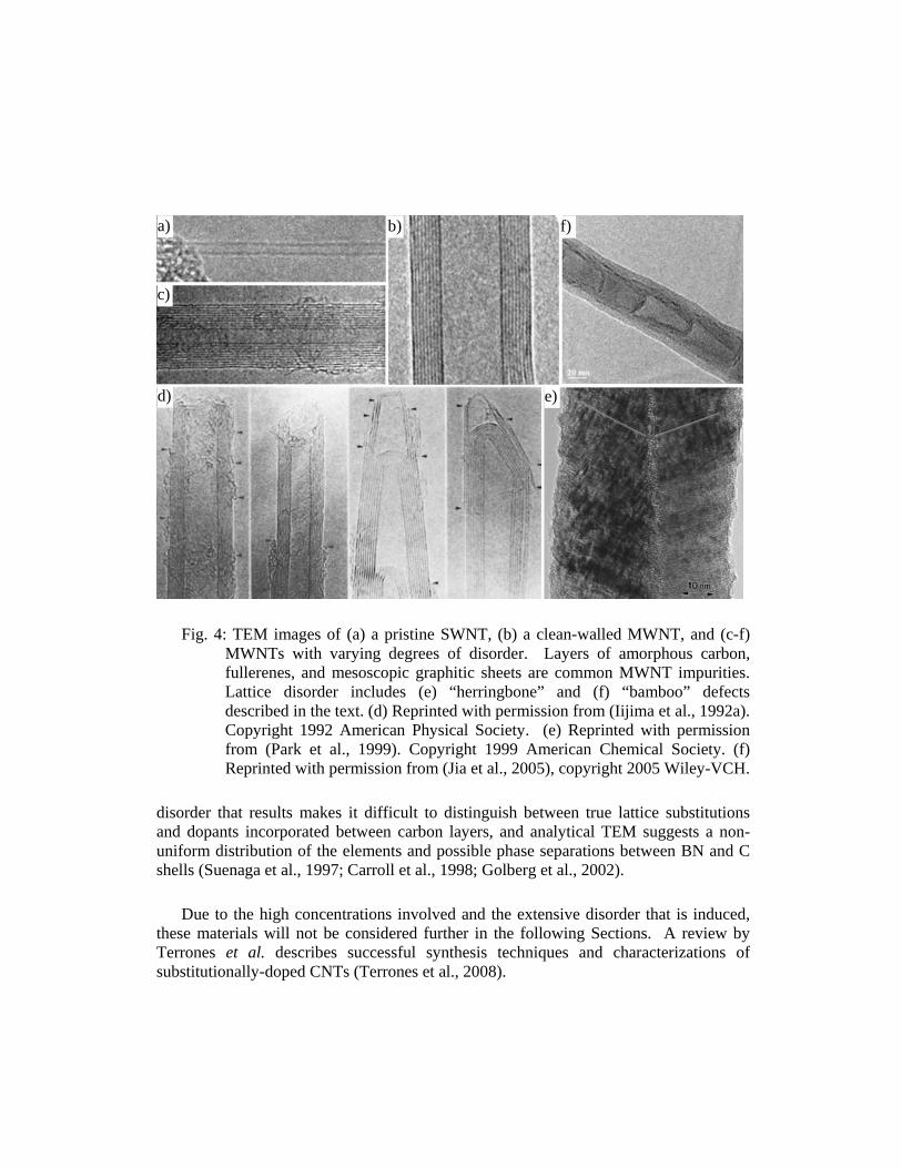
Fig. 4: TEM images of (a) a pristine SWNT, (b) a clean-walled MWNT, and (c-f) MWNTs with varying degrees of disorder. Layers of amorphous carbon, fullerenes, and mesoscopic graphitic sheets are common MWNT impurities. Lattice disorder includes (e) “herringbone” and (f) “bamboo” defects described in the text. (d) Reprinted with permission from (Iijima et al., 1992a). Copyright 1992 American Physical Society. (e) Reprinted with permission from (Park et al., 1999). Copyright 1999 American Chemical Society. (f) Reprinted with permission from (Jia et al., 2005), copyright 2005 Wiley-VCH.
disorder that results makes it difficult to distinguish between true lattice substitutions and dopants incorporated between carbon layers, and analytical TEM suggests a non-uniform distribution of the elements and possible phase separations between BN and C shells (Suenaga et al., 1997; Carroll et al., 1998; Golberg et al., 2002).
Due to the high concentrations involved and the extensive disorder that is induced, these materials will not be considered further in the following Sections. A review by Terrones et al. describes successful synthesis techniques and characterizations of substitutionally-doped CNTs (Terrones et al., 2008).
a) b)
c)
d) e)
f)
3. EXPERIMENTAL IDENTIFICATION OF DEFECTS
The next Section of this review summarizes the development of experimental methods for locating defects in CNTs. The intent is to provide both historical context and a guide for continued investigation. The techniques described in this section are roughly organized in order of precision, from atomic resolution scanning tunneling microscopy (STM) to more indirect measures of defect density by optical and electronic techniques. It is immediately apparent that locating defects with high precision is inversely correlated with yield: the highest precision techniques are painstaking and unable to categorize defect densities with good statistics. As a group, the techniques are highly complementary and progress in the identification, categorization, and control of CNT defects is likely to take advantage of the entire suite of methods.
3.1. Scanning tunneling microscopy
STM is one of the highest resolution tools in the experimentalists’ toolkit. The issue of finding and characterizing defects therefore seems naturally suited to STM, especially for an all-surface material like SWNTs. Where conventional bulk techniques might fail to distinguish a single point defect or its physical effects, one might expect STM to provide decisive insights.
In practice, however, this idealization has proven very difficult. Early work imaging CNTs routinely failed to achieve atomic resolution, in part because of the difficulties of clean sample preparation. A SWNT’s diameter is equal to only a few, monatomic metal steps, and when deposited from solution, all CNTs assemble with codeposited carbonaceous adsorbates and solubilized contaminants. By using highly purified suspensions, one can achieve dilute dispersions in which isolated CNTs are only bound to the surface by weak van der Waals forces. However, in this “pristine” state, small electrostatic forces readily move CNTs on a surface (Falvo et al., 1999), often precluding the tunneling conditions necessary for atomic resolution.
Researchers developed various solutions for overcoming these experimental challenges. In the earliest work, MWNTs (Ge and Sattler, 1993) and SWNTs (Ge and Sattler, 1994) were directly condensed from a carbon plasma onto cleaved graphite surfaces for imaging. A more versatile technique used deposition from suspensions of SWNTs. Partly solubilized SWNTs in parallel bundles are stabilized by increased van der Waals attractions that help anchor them in place during imaging, reducing their tendency to roll on the surface and allowing for atomic resolution. This solution has been widely employed to study the correspondence between SWNT chirality and electronic band structure (Wildoer et al., 1998; Odom et al., 1998; Hassanien et al., 1998), and has resulted in the observation of CNT defects (Clauss et al., 1998; Clauss et
al., 1999). A third solution to sample preparation has leveraged progress in synthetic CVD techniques to grow clean and isolated SWNTs in place on a substrate. Using CVD, CNTs free of any chemical processing can be imaged on various substrates (Biro et al., 1997) or even freely suspended across gaps (LeRoy et al., 2004b). Advantages of pristine SWNTs include the opportunity to directly image as-grown defects, and the ability of very long SWNTs to more effectively pin themselves to a surface for imaging. Unfortunately, experimental STM results on such pristine SWNTs are limited because CVD growth of SWNTs is mostly confined to insulating substrates.
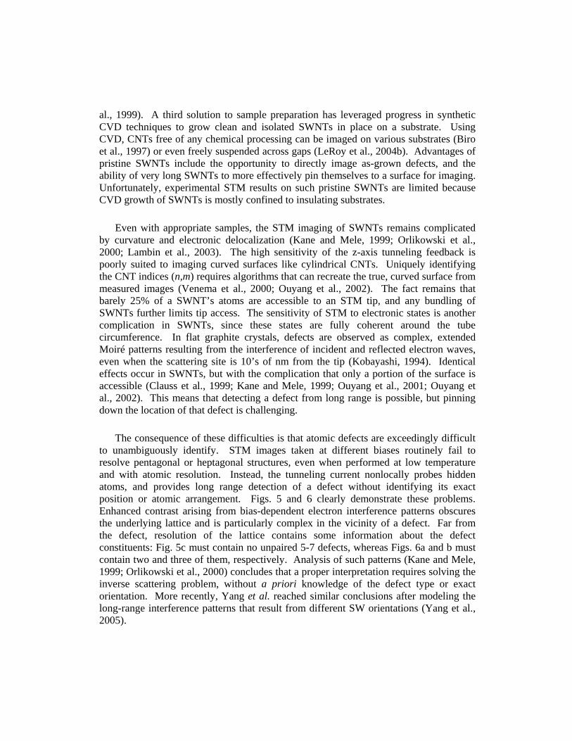
Even with appropriate samples, the STM imaging of SWNTs remains complicated by curvature and electronic delocalization (Kane and Mele, 1999; Orlikowski et al., 2000; Lambin et al., 2003). The high sensitivity of the z-axis tunneling feedback is poorly suited to imaging curved surfaces like cylindrical CNTs. Uniquely identifying the CNT indices (n,m) requires algorithms that can recreate the true, curved surface from measured images (Venema et al., 2000; Ouyang et al., 2002). The fact remains that barely 25% of a SWNT’s atoms are accessible to an STM tip, and any bundling of SWNTs further limits tip access. The sensitivity of STM to electronic states is another complication in SWNTs, since these states are fully coherent around the tube circumference. In flat graphite crystals, defects are observed as complex, extended Moiré patterns resulting from the interference of incident and reflected electron waves, even when the scattering site is 10’s of nm from the tip (Kobayashi, 1994). Identical effects occur in SWNTs, but with the complication that only a portion of the surface is accessible (Clauss et al., 1999; Kane and Mele, 1999; Ouyang et al., 2001; Ouyang et al., 2002). This means that detecting a defect from long range is possible, but pinning down the location of that defect is challenging.
The consequence of these difficulties is that atomic defects are exceedingly difficult to unambiguously identify. STM images taken at different biases routinely fail to resolve pentagonal or heptagonal structures, even when performed at low temperature and with atomic resolution. Instead, the tunneling current nonlocally probes hidden atoms, and provides long range detection of a defect without identifying its exact position or atomic arrangement. Figs. 5 and 6 clearly demonstrate these problems. Enhanced contrast arising from bias-dependent electron interference patterns obscures the underlying lattice and is particularly complex in the vicinity of a defect. Far from the defect, resolution of the lattice contains some information about the defect constituents: Fig. 5c must contain no unpaired 5-7 defects, whereas Figs. 6a and b must contain two and three of them, respectively. Analysis of such patterns (Kane and Mele, 1999; Orlikowski et al., 2000) concludes that a proper interpretation requires solving the inverse scattering problem, without a priori knowledge of the defect type or exact orientation. More recently, Yang et al. reached similar conclusions after modeling the long-range interference patterns that result from different SW orientations (Yang et al., 2005).
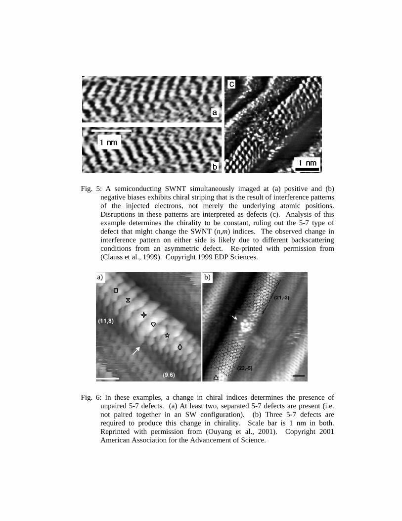
Fig. 5: A semiconducting SWNT simultaneously imaged at (a) positive and (b) negative biases exhibits chiral striping that is the result of interference patterns of the injected electrons, not merely the underlying atomic positions. Disruptions in these patterns are interpreted as defects (c). Analysis of this example determines the chirality to be constant, ruling out the 5-7 type of defect that might change the SWNT (n,m) indices. The observed change in interference pattern on either side is likely due to different backscattering conditions from an asymmetric defect. Re-printed with permission from (Clauss et al., 1999). Copyright 1999 EDP Sciences.
Fig. 6: In these examples, a change in chiral indices determines the presence of unpaired 5-7 defects. (a) At least two, separated 5-7 defects are present (i.e. not paired together in an SW configuration). (b) Three 5-7 defects are required to produce this change in chirality. Scale bar is 1 nm in both. Reprinted with permission from (Ouyang et al., 2001). Copyright 2001 American Association for the Advancement of Science.
a) b)
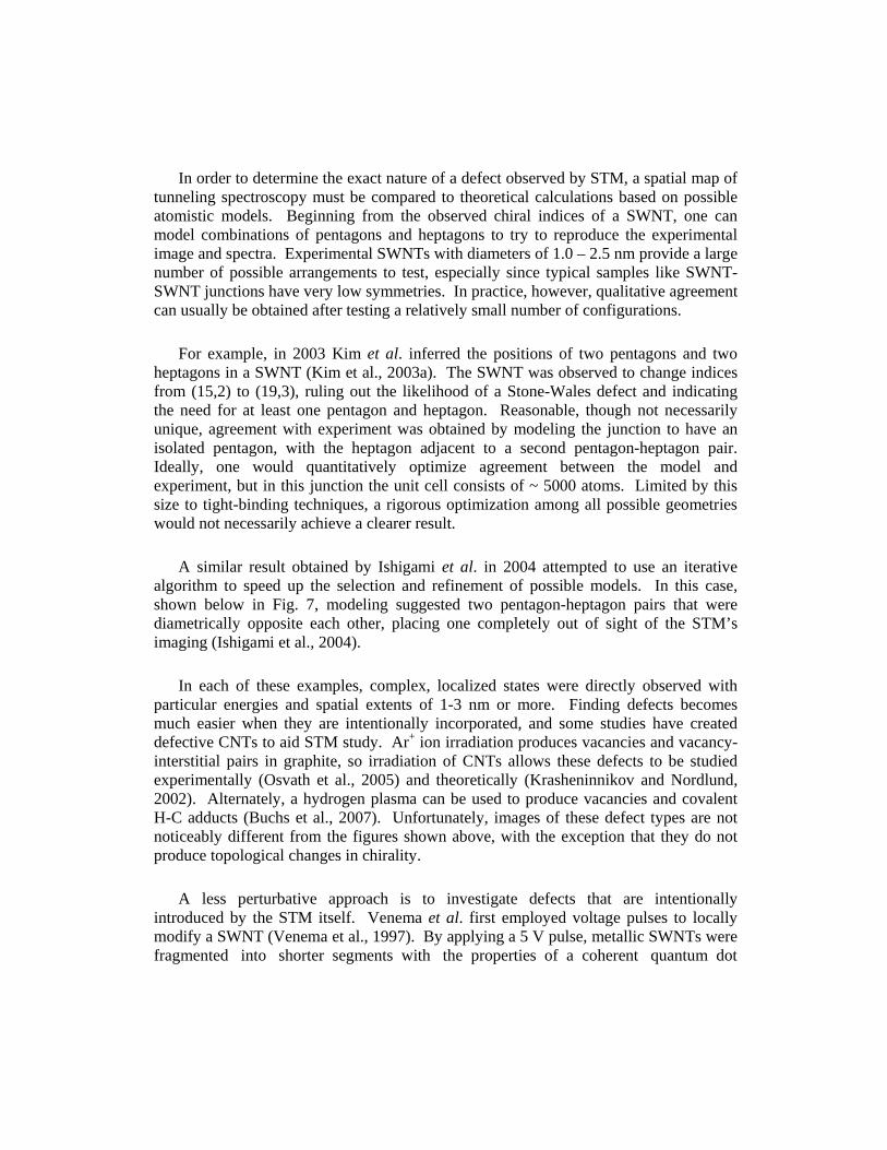
In order to determine the exact nature of a defect observed by STM, a spatial map of tunneling spectroscopy must be compared to theoretical calculations based on possible atomistic models. Beginning from the observed chiral indices of a SWNT, one can model combinations of pentagons and heptagons to try to reproduce the experimental image and spectra. Experimental SWNTs with diameters of 1.0 – 2.5 nm provide a large number of possible arrangements to test, especially since typical samples like SWNT-SWNT junctions have very low symmetries. In practice, however, qualitative agreement can usually be obtained after testing a relatively small number of configurations.
For example, in 2003 Kim et al. inferred the positions of two pentagons and two heptagons in a SWNT (Kim et al., 2003a). The SWNT was observed to change indices from (15,2) to (19,3), ruling out the likelihood of a Stone-Wales defect and indicating the need for at least one pentagon and heptagon. Reasonable, though not necessarily unique, agreement with experiment was obtained by modeling the junction to have an isolated pentagon, with the heptagon adjacent to a second pentagon-heptagon pair. Ideally, one would quantitatively optimize agreement between the model and experiment, but in this junction the unit cell consists of ~ 5000 atoms. Limited by this size to tight-binding techniques, a rigorous optimization among all possible geometries would not necessarily achieve a clearer result.
A similar result obtained by Ishigami et al. in 2004 attempted to use an iterative algorithm to speed up the selection and refinement of possible models. In this case, shown below in Fig. 7, modeling suggested two pentagon-heptagon pairs that were diametrically opposite each other, placing one completely out of sight of the STM’s imaging (Ishigami et al., 2004).
In each of these examples, complex, localized states were directly observed with particular energies and spatial extents of 1-3 nm or more. Finding defects becomes much easier when they are intentionally incorporated, and some studies have created defective CNTs to aid STM study. Ar+ ion irradiation produces vacancies and vacancy-interstitial pairs in graphite, so irradiation of CNTs allows these defects to be studied experimentally (Osvath et al., 2005) and theoretically (Krasheninnikov and Nordlund, 2002). Alternately, a hydrogen plasma can be used to produce vacancies and covalent H-C adducts (Buchs et al., 2007). Unfortunately, images of these defect types are not noticeably different from the figures shown above, with the exception that they do not produce topological changes in chirality.
A less perturbative approach is to investigate defects that are intentionally introduced by the STM itself. Venema et al. first employed voltage pulses to locally modify a SWNT (Venema et al., 1997). By applying a 5 V pulse, metallic SWNTs were fragmented into shorter segments with the properties of a coherent quantum dot
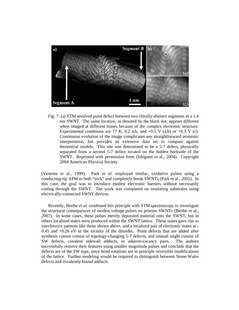
Fig. 7: (a) STM resolved point defect between two chirally-distinct segments in a 1.4 nm SWNT. The same location, as denoted by the black dot, appears different when imaged at different biases because of the complex electronic structure. Experimental conditions are 77 K, 0.2 nA, and +0.5 V (a,b) or +0.3 V (c). Continuous evolution of the image complicates any straightforward atomistic interpretation, but provides an extensive data set to compare against theoretical models. This site was determined to be a 5-7 defect, physically separated from a second 5-7 defect located on the hidden backside of the SWNT. Reprinted with permission from (Ishigami et al., 2004). Copyright 2004 American Physical Society.
(Venema et al., 1999). Park et al. employed similar, oxidative pulses using a conducting-tip AFM to both “nick” and completely break SWNTs (Park et al., 2002). In this case, the goal was to introduce modest electronic barriers without necessarily cutting through the SWNT. The work was completed on insulating substrates using electrically-connected SWNT devices.
Recently, Berthe et al. combined this principle with STM spectroscopy to investigate the structural consequences of modest voltage pulses on pristine SWNTs (Berthe et al., 2007). In some cases, these pulses merely deposited material onto the SWNT, but in others localized states were produced within the SWNT lattice. These states gave rise to interference patterns like those shown above, and a localized pair of electronic states at -0.45 and +0.26 eV in the vicinity of the disorder. Point defects that are added after synthesis cannot consist of topology-changing 5-7 defects, and instead might consist of SW defects, covalent sidewall adducts, or adatom-vacancy pairs. The authors successfully remove their features using smaller magnitude pulses and conclude that the defects are of the SW type, since bond rotations are in principle reversible modifications of the lattice. Further modeling would be required to distinguish between Stone-Wales defects and covalently bound adducts.
b)
c)
a)

An alternate use of STM spectroscopy is to look at inelastic tunneling spectroscopy (IETS). Unlike the elastic spectroscopy, which primarily measures the electronic van Hove singularities, IETS is sensitive to dissipative channels including localized phonon modes. Experimentally challenging, IETS measurements on SWNTs have nonetheless measured low energy modes associated with defects or dissipation through the radial breathing mode (Vitali et al., 2004; LeRoy et al., 2004a). Recent theoretical modeling predicts energetic shifts of +20 cm-1 for the C-C bond in a Stone-Wales defect, and -50 cm-1 shifts around isotopic C13 impurities (Vandescuren et al., 2007). The latter type of disorder is particularly difficult to study by any other experimental means.
Despite providing extraordinary precision, the STM techniques are not building a library of ready images that can categorize different defect types. If anything, the defects characterized by Ouyang, Kim, and Ishigami were readily modeled because of a change in SWNT chirality; but the majority of SWNT defects, including adducts and SW bond rotations, do not change the underlying SWNT lattice. These may be much more difficult to locate and uniquely identify. Finding the rare, tractable defect by STM, combined with the degree of work required to model it, may never improve into a particularly efficient way of categorizing CNT defects and defect densities. While promising, Ishigami et al. note that their modeling only accounts for “the atomic structure of the most dominant defect,” leaving open the possibility of additional atomic disorder hidden within these complex images.
3.2. Electron microscopy
STM may be most closely associated with atomic resolution imaging, but transmission electron microscopy (TEM) is unquestionably the primary tool for characterizing CNTs. TEM is responsible for the initial identification of CNTs, for characterizing CNT growth, and for understanding the complex morphologies of MWNTs. Until recently, however, TEM imaging has not been associated with the kind of resolution necessary for studying individual point defects in any material, much less CNTs.
CNTs present a special challenge to TEM resolution because of carbon’s small atomic number. Most common TEM instruments remain blind to a single graphene layer normal to the electron beam. Image contrast for CNTs instead arises fortuitously from their cylindrical geometry (Iijima, 1991). While the beam’s interaction with much of a CNT is negligible, the extreme CNT edges provide a lattice parallel to the electron beam for which diffraction conditions exist. Iijima and other early practitioners took advantage of these conditions to produce the first clear CNT images and to convince the community that these materials were indeed hollow cylinders (Fig. 8). In time, the common images of two parallel lines became synonymous with the accepted CNT structure. The presence of extraneous material, however, complicated image
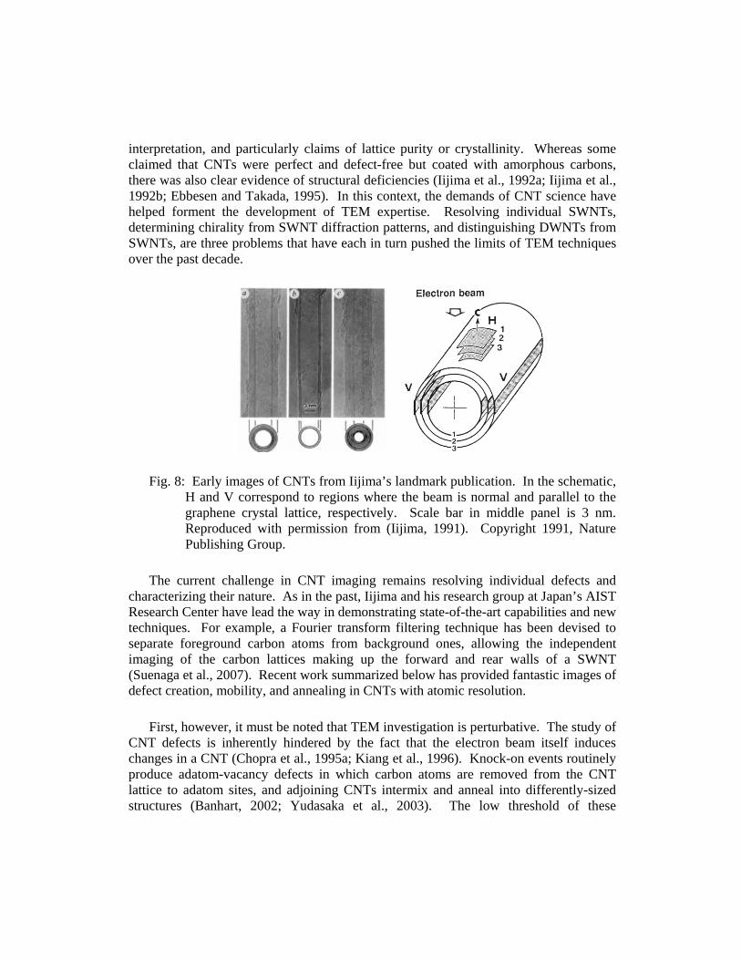
interpretation, and particularly claims of lattice purity or crystallinity. Whereas some claimed that CNTs were perfect and defect-free but coated with amorphous carbons, there was also clear evidence of structural deficiencies (Iijima et al., 1992a; Iijima et al., 1992b; Ebbesen and Takada, 1995). In this context, the demands of CNT science have helped forment the development of TEM expertise. Resolving individual SWNTs, determining chirality from SWNT diffraction patterns, and distinguishing DWNTs from SWNTs, are three problems that have each in turn pushed the limits of TEM techniques over the past decade.
Fig. 8: Early images of CNTs from Iijima’s landmark publication. In the schematic, H and V correspond to regions where the beam is normal and parallel to the graphene crystal lattice, respectively. Scale bar in middle panel is 3 nm. Reproduced with permission from (Iijima, 1991). Copyright 1991, Nature Publishing Group.
The current challenge in CNT imaging remains resolving individual defects and characterizing their nature. As in the past, Iijima and his research group at Japan’s AIST Research Center have lead the way in demonstrating state-of-the-art capabilities and new techniques. For example, a Fourier transform filtering technique has been devised to separate foreground carbon atoms from background ones, allowing the independent imaging of the carbon lattices making up the forward and rear walls of a SWNT (Suenaga et al., 2007). Recent work summarized below has provided fantastic images of defect creation, mobility, and annealing in CNTs with atomic resolution.
First, however, it must be noted that TEM investigation is perturbative. The study of CNT defects is inherently hindered by the fact that the electron beam itself induces changes in a CNT (Chopra et al., 1995a; Kiang et al., 1996). Knock-on events routinely produce adatom-vacancy defects in which carbon atoms are removed from the CNT lattice to adatom sites, and adjoining CNTs intermix and anneal into differently-sized structures (Banhart, 2002; Yudasaka et al., 2003). The low threshold of these
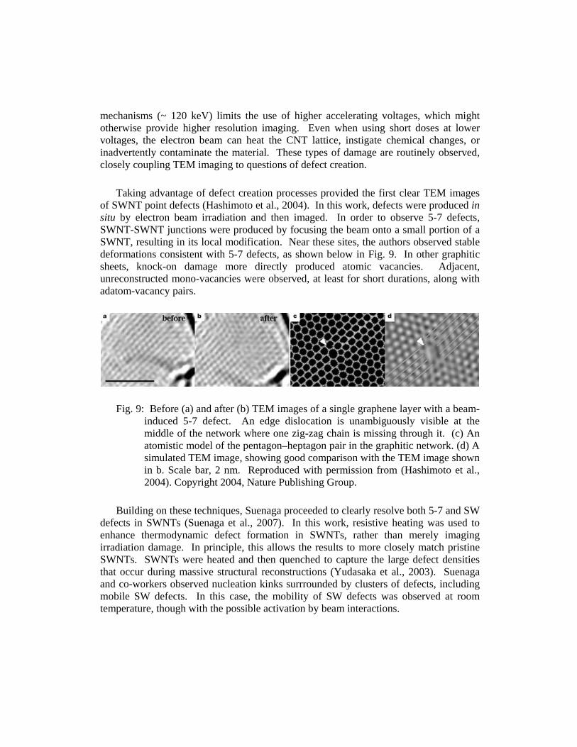
mechanisms (~ 120 keV) limits the use of higher accelerating voltages, which might otherwise provide higher resolution imaging. Even when using short doses at lower voltages, the electron beam can heat the CNT lattice, instigate chemical changes, or inadvertently contaminate the material. These types of damage are routinely observed, closely coupling TEM imaging to questions of defect creation.
Taking advantage of defect creation processes provided the first clear TEM images of SWNT point defects (Hashimoto et al., 2004). In this work, defects were produced in situ by electron beam irradiation and then imaged. In order to observe 5-7 defects, SWNT-SWNT junctions were produced by focusing the beam onto a small portion of a SWNT, resulting in its local modification. Near these sites, the authors observed stable deformations consistent with 5-7 defects, as shown below in Fig. 9. In other graphitic sheets, knock-on damage more directly produced atomic vacancies. Adjacent, unreconstructed mono-vacancies were observed, at least for short durations, along with adatom-vacancy pairs.
Fig. 9: Before (a) and after (b) TEM images of a single graphene layer with a beam-induced 5-7 defect. An edge dislocation is unambiguously visible at the middle of the network where one zig-zag chain is missing through it. (c) An atomistic model of the pentagon–heptagon pair in the graphitic network. (d) A simulated TEM image, showing good comparison with the TEM image shown in b. Scale bar, 2 nm. Reproduced with permission from (Hashimoto et al., 2004). Copyright 2004, Nature Publishing Group.
Building on these techniques, Suenaga proceeded to clearly resolve both 5-7 and SW defects in SWNTs (Suenaga et al., 2007). In this work, resistive heating was used to enhance thermodynamic defect formation in SWNTs, rather than merely imaging irradiation damage. In principle, this allows the results to more closely match pristine SWNTs. SWNTs were heated and then quenched to capture the large defect densities that occur during massive structural reconstructions (Yudasaka et al., 2003). Suenaga and co-workers observed nucleation kinks surrrounded by clusters of defects, including mobile SW defects. In this case, the mobility of SW defects was observed at room temperature, though with the possible activation by beam interactions.
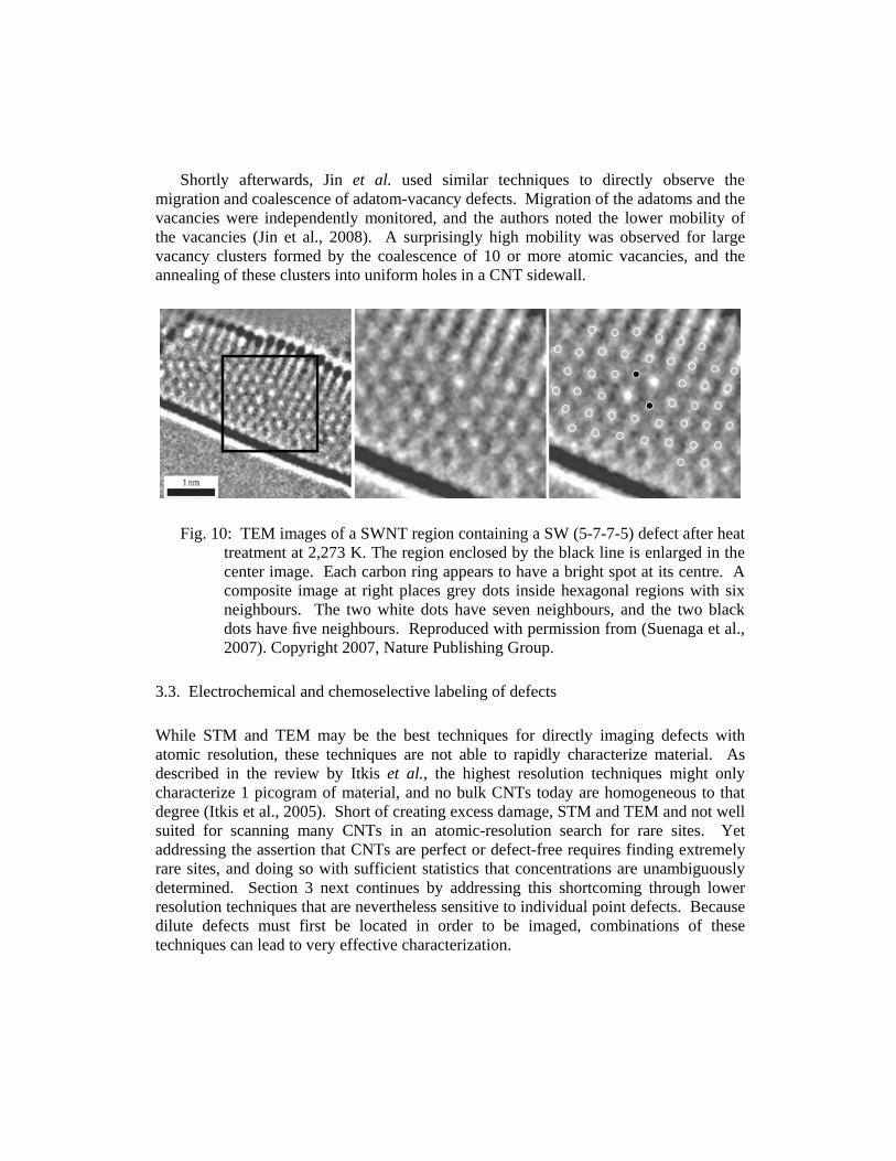
Shortly afterwards, Jin et al. used similar techniques to directly observe the migration and coalescence of adatom-vacancy defects. Migration of the adatoms and the vacancies were independently monitored, and the authors noted the lower mobility of the vacancies (Jin et al., 2008). A surprisingly high mobility was observed for large vacancy clusters formed by the coalescence of 10 or more atomic vacancies, and the annealing of these clusters into uniform holes in a CNT sidewall.
Fig. 10: TEM images of a SWNT region containing a SW (5-7-7-5) defect after heat treatment at 2,273 K. The region enclosed by the black line is enlarged in the center image. Each carbon ring appears to have a bright spot at its centre. A composite image at right places grey dots inside hexagonal regions with six neighbours. The two white dots have seven neighbours, and the two black dots have five neighbours. Reproduced with permission from (Suenaga et al., 2007). Copyright 2007, Nature Publishing Group.
3.3. Electrochemical and chemoselective labeling of defects
While STM and TEM may be the best techniques for directly imaging defects with atomic resolution, these techniques are not able to rapidly characterize material. As described in the review by Itkis et al., the highest resolution techniques might only characterize 1 picogram of material, and no bulk CNTs today are homogeneous to that degree (Itkis et al., 2005). Short of creating excess damage, STM and TEM and not well suited for scanning many CNTs in an atomic-resolution search for rare sites. Yet addressing the assertion that CNTs are perfect or defect-free requires finding extremely rare sites, and doing so with sufficient statistics that concentrations are unambiguously determined. Section 3 next continues by addressing this shortcoming through lower resolution techniques that are nevertheless sensitive to individual point defects. Because dilute defects must first be located in order to be imaged, combinations of these techniques can lead to very effective characterization.
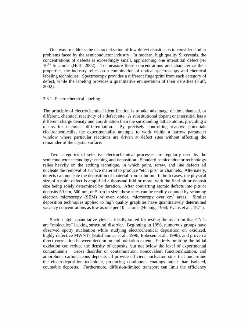
One way to address the characterization of low defect densities is to consider similar problems faced by the semiconductor industry. In modern, high quality Si crystals, the concentrations of defects is exceedingly small, approaching one interstitial defect per 1013 Si atoms (Huff, 2002). To measure these concentrations and characterize their properties, the industry relies on a combination of optical spectroscopy and chemical labeling techniques. Spectroscopy provides a different fingerprint from each category of defect, while the labeling provides a quantitative enumeration of their densities (Huff, 2002).
3.3.1 Electrochemical labeling
The principle of electrochemical identification is to take advantage of the enhanced, or different, chemical reactivity of a defect site. A substitutional dopant or interstitial has a different charge density and coordination than the surrounding lattice atoms, providing a means for chemical differentiation. By precisely controlling reactive potentials electrochemically, the experimentalist attempts to work within a narrow parameter window where particular reactions are driven at defect sites without affecting the remainder of the crystal surface.
Two categories of selective electrochemical processes are regularly used by the semiconductor technology: etching and deposition. Standard semiconductor technology relies heavily on the etching technique, in which point, screw, and line defects all nucleate the removal of surface material to produce “etch pits” or channels. Alternately, defects can nucleate the deposition of material from solution. In both cases, the physical size of a point defect is amplified a thousand fold or more, with the final pit or deposit size being solely determined by duration. After converting atomic defects into pits or deposits 50 nm, 500 nm, or 5 μm in size, these sites can be readily counted by scanning electron microscopy (SEM) or even optical microscopy over cm2 areas. Similar deposition techniques applied to high quality graphites have quantitatively determined vacancy concentrations as low as one per 1010 atoms (Hennig, 1964; Evans et al., 1971).
Such a high, quantitative yield is ideally suited for testing the assertion that CNTs are “molecules” lacking structural disorder. Beginning in 1996, numerous groups have observed spotty nucleation while studying electrochemical deposition on oxidized, highly defective MWNTs (Satishkumar et al., 1996; Ebbesen et al., 1996), and proven a direct correlation between decoration and oxidation extent. Entirely omitting the initial oxidation can reduce the density of deposits, but not below the level of experimental contaminants. Gross disorder or contamination, noncovalent functionalization, and amorphous carbonaceous deposits all provide efficient nucleation sites that undermine the electrodeposition technique, producing continuous coatings rather than isolated, countable deposits. Furthermore, diffusion-limited transport can limit the efficiency
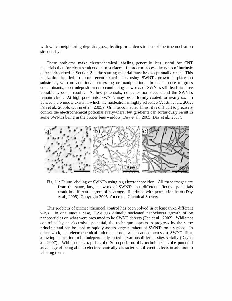
with which neighboring deposits grow, leading to underestimates of the true nucleation site density.
These problems make electrochemical labeling generally less useful for CNT materials than for clean semiconductor surfaces. In order to access the types of intrinsic defects described in Section 2.1, the starting material must be exceptionally clean. This realization has led to more recent experiments using SWNTs grown in place on substrates, with no additional processing or manipulation. In the absence of gross contaminants, electrodeposition onto conducting networks of SWNTs still leads to three possible types of results. At low potentials, no deposition occurs and the SWNTs remain clean. At high potentials, SWNTs may be uniformly coated, or nearly so. In between, a window exists in which the nucleation is highly selective (Austin et al., 2002; Fan et al., 2005b; Quinn et al., 2005). On interconnected films, it is difficult to precisely control the electrochemical potential everywhere, but gradients can fortuitously result in some SWNTs being in the proper bias window (Day et al., 2005; Day et al., 2007).
Fig. 11: Dilute labeling of SWNTs using Ag electrodeposition. All three images are from the same, large network of SWNTs, but different effective potentials result in different degrees of coverage. Reprinted with permission from (Day et al., 2005). Copyright 2005, American Chemical Society.
This problem of precise chemical control has been solved in at least three different ways. In one unique case, H2Se gas dilutely nucleated nanocluster growth of Se nanoparticles on what were presumed to be SWNT defects (Fan et al., 2002). While not controlled by an electrolyte potential, the technique appears to progress by the same principle and can be used to rapidly assess large numbers of SWNTs on a surface. In other work, an electrochemical microelectrode was scanned across a SWNT film, allowing deposition to be independently tested at various different sites serially (Day et al., 2007). While not as rapid as the Se deposition, this technique has the potential advantage of being able to electrochemically characterize different defects in addition to labeling them.
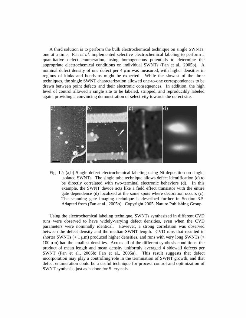
A third solution is to perform the bulk electrochemical technique on single SWNTs, one at a time. Fan et al. implemented selective electrochemical labeling to perform a quantitative defect enumeration, using homogeneous potentials to determine the appropriate electrochemical conditions on individual SWNTs (Fan et al., 2005b). A nominal defect density of one defect per 4 μm was measured, with higher densities in regions of kinks and bends as might be expected. While the slowest of the three techniques, the single SWNT characterization allowed one-to-one correspondences to be drawn between point defects and their electronic consequences. In addition, the high level of control allowed a single site to be labeled, stripped, and reproducibly labeled again, providing a convincing demonstration of selectivity towards the defect site.
Fig. 12: (a,b) Single defect electrochemical labeling using Ni deposition on single, isolated SWNTs. The single tube technique allows defect identification (c) to be directly correlated with two-terminal electronic behaviors (d). In this example, the SWNT device acts like a field effect transistor with the entire gate dependence (d) localized at the same spots where decoration occurs (c). The scanning gate imaging technique is described further in Section 3.5. Adapted from (Fan et al., 2005b). Copyright 2005, Nature Publishing Group.
Using the electrochemical labeling technique, SWNTs synthesized in different CVD runs were observed to have widely-varying defect densities, even when the CVD parameters were nominally identical. However, a strong correlation was observed between the defect density and the median SWNT length. CVD runs that resulted in shorter SWNTs (< 1 μm) produced higher densities, and runs with very long SWNTs (> 100 μm) had the smallest densities. Across all of the different synthesis conditions, the product of mean length and mean density uniformly averaged 4 sidewall defects per SWNT (Fan et al., 2005b; Fan et al., 2005a). This result suggests that defect incorporation may play a controlling role in the termination of SWNT growth, and that defect enumeration could be a useful technique for process control and optimization of SWNT synthesis, just as is done for Si crystals.
Even on isolated SWNTs, a degree of imprecision remains because different defect types are indistinguishable. Certain bond rotations or adducts might only be slightly different in reactivity, and experimental errors limit the practical electrochemical windows for selecting individual types. Furthermore, it is impractical to rigorously clean surfaces supporting SWNTs. By comparison, etch pits on Si crystals are relatively straightforward to interpret because depth profiling is first used to expose pristine surfaces within the crystal. This step has the benefit of removing extraneous surface contaminants that might mimic the reactivity of defects. In the case of SWNTs, any species that is electronically well-connected to the SWNT can be labeled. Thus, in addition to lattice defects and covalent adducts, nucleation may occur because of charged contaminants trapped at the SWNT-substrate interface or also shallow charge traps in the dielectric immediately supporting a SWNT. As described in Section 2.2, these sites are not defects in the conventional sense but they are present in the majority of CNT research. Thus labeling and counting these sites is appropriate in practice if they interact with and affect chemical and electronic behaviors.
3.3.2 Chemoselective labeling
While the electrochemical techniques described above are not particularly sensitive to different defect types, other reactions are more selective. A careful series of titrations using NaHCO3, Na2CO3, and finally NaOH can quantitatively determine the concentrations of different oxygen-containing groups in bulk graphites, distinguishing between carboxyls, phenols, and carbonyls (Donnet, 1968; Kinoshita, 1988). Even SW defects have a higher reactivity than their surrounding hexagonal rings (Liu et al., 2006b; Horner et al., 2007; Wang et al., 2006). Though small defect concentrations in CNTs cannot be effectively titrated in the presence of endcaps and other disorder, selective reactions can be used as an initial step to activate defect sites for subsequent labeling and detection.
For example, ozone is believed to be highly reactive at SW defect and vacancy sites, whereas the pristine sidewall forms only an unstable, short-lived complex (Banerjee and Wong, 2002; Liu et al., 2006b). Other oxidants, including KMnO4
-, OsO4, and RuO4, are relatively efficient at cleaving C-C bonds in the vicinity of a defect or endcap, but do not readily attack the sidewall at room temperature (Hwang, 1995; Coroneus et al., 2008). These oxidations can produce carboxylic groups, a unique form of defect that can be chemically tailored. In particular, carboxylates have a highly selective reaction with the reagents N-ethyl-N'-(3-dimethylaminopropyl) carbodiimide (EDC) and N-hydroxysuccinimide (NHS). Following reaction, the NHS ester is readily displaced from the carboxylate by any molecule with an amine attachment site, providing a direct, versatile, and high yield route for selective labeling by a wide range of molecules (Grabarek and Gergely, 1990; Banerjee et al., 2005). Fig. 13 demonstrates an example of this attachment process. The EDC/NHS protocol has been used to covalently bind the
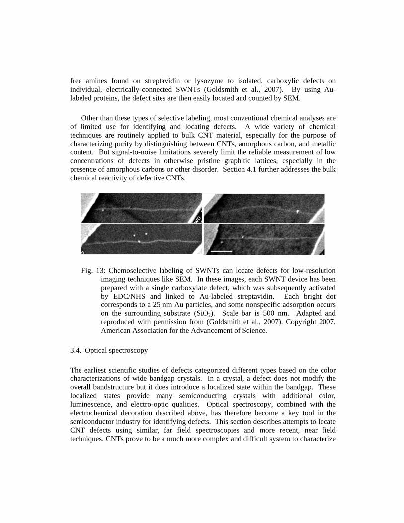
free amines found on streptavidin or lysozyme to isolated, carboxylic defects on individual, electrically-connected SWNTs (Goldsmith et al., 2007). By using Au-labeled proteins, the defect sites are then easily located and counted by SEM.
Other than these types of selective labeling, most conventional chemical analyses are of limited use for identifying and locating defects. A wide variety of chemical techniques are routinely applied to bulk CNT material, especially for the purpose of characterizing purity by distinguishing between CNTs, amorphous carbon, and metallic content. But signal-to-noise limitations severely limit the reliable measurement of low concentrations of defects in otherwise pristine graphitic lattices, especially in the presence of amorphous carbons or other disorder. Section 4.1 further addresses the bulk chemical reactivity of defective CNTs.
Fig. 13: Chemoselective labeling of SWNTs can locate defects for low-resolution imaging techniques like SEM. In these images, each SWNT device has been prepared with a single carboxylate defect, which was subsequently activated by EDC/NHS and linked to Au-labeled streptavidin. Each bright dot corresponds to a 25 nm Au particles, and some nonspecific adsorption occurs on the surrounding substrate (SiO2). Scale bar is 500 nm. Adapted and reproduced with permission from (Goldsmith et al., 2007). Copyright 2007, American Association for the Advancement of Science.
3.4. Optical spectroscopy
The earliest scientific studies of defects categorized different types based on the color characterizations of wide bandgap crystals. In a crystal, a defect does not modify the overall bandstructure but it does introduce a localized state within the bandgap. These localized states provide many semiconducting crystals with additional color, luminescence, and electro-optic qualities. Optical spectroscopy, combined with the electrochemical decoration described above, has therefore become a key tool in the semiconductor industry for identifying defects. This section describes attempts to locate CNT defects using similar, far field spectroscopies and more recent, near field techniques. CNTs prove to be a much more complex and difficult system to characterize
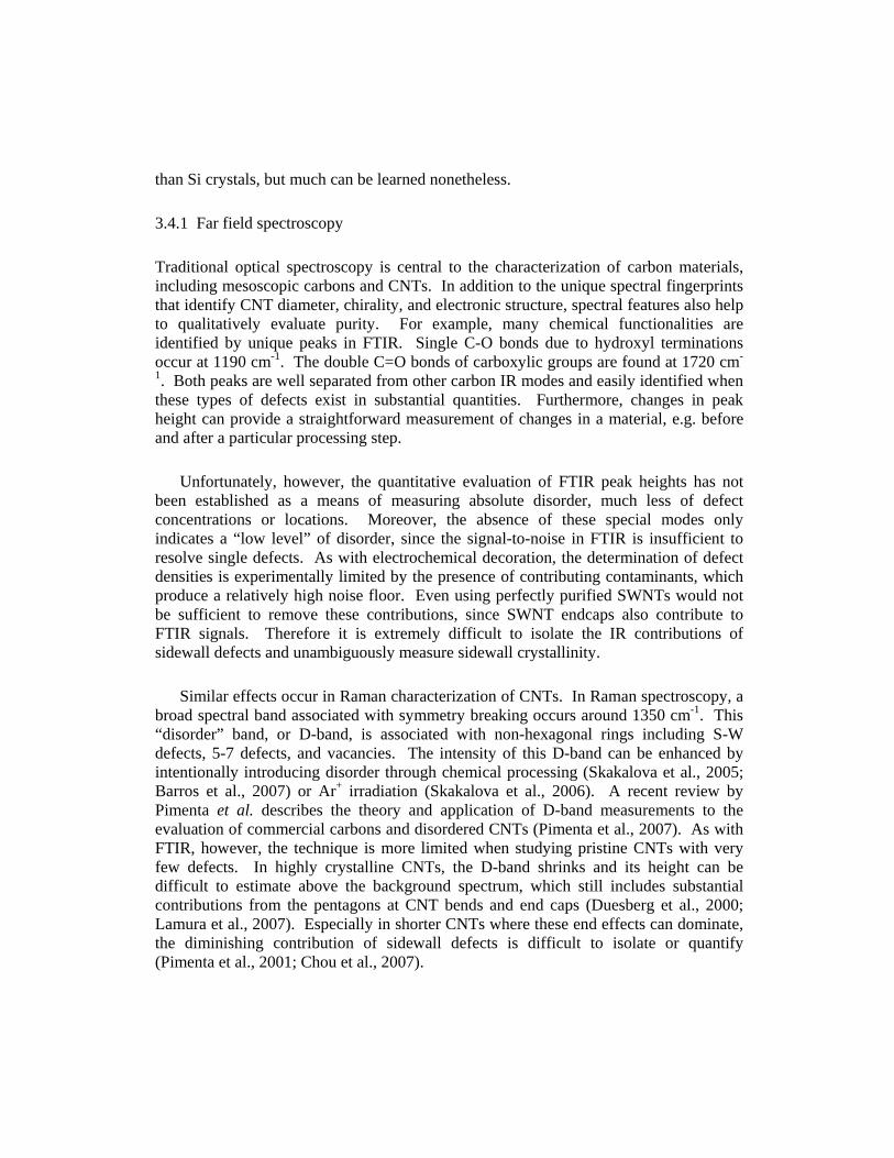
than Si crystals, but much can be learned nonetheless.
3.4.1 Far field spectroscopy
Traditional optical spectroscopy is central to the characterization of carbon materials, including mesoscopic carbons and CNTs. In addition to the unique spectral fingerprints that identify CNT diameter, chirality, and electronic structure, spectral features also help to qualitatively evaluate purity. For example, many chemical functionalities are identified by unique peaks in FTIR. Single C-O bonds due to hydroxyl terminations occur at 1190 cm-1. The double C=O bonds of carboxylic groups are found at 1720 cm-
1. Both peaks are well separated from other carbon IR modes and easily identified when these types of defects exist in substantial quantities. Furthermore, changes in peak height can provide a straightforward measurement of changes in a material, e.g. before and after a particular processing step.
Unfortunately, however, the quantitative evaluation of FTIR peak heights has not been established as a means of measuring absolute disorder, much less of defect concentrations or locations. Moreover, the absence of these special modes only indicates a “low level” of disorder, since the signal-to-noise in FTIR is insufficient to resolve single defects. As with electrochemical decoration, the determination of defect densities is experimentally limited by the presence of contributing contaminants, which produce a relatively high noise floor. Even using perfectly purified SWNTs would not be sufficient to remove these contributions, since SWNT endcaps also contribute to FTIR signals. Therefore it is extremely difficult to isolate the IR contributions of sidewall defects and unambiguously measure sidewall crystallinity.
Similar effects occur in Raman characterization of CNTs. In Raman spectroscopy, a broad spectral band associated with symmetry breaking occurs around 1350 cm-1. This “disorder” band, or D-band, is associated with non-hexagonal rings including S-W defects, 5-7 defects, and vacancies. The intensity of this D-band can be enhanced by intentionally introducing disorder through chemical processing (Skakalova et al., 2005; Barros et al., 2007) or Ar+ irradiation (Skakalova et al., 2006). A recent review by Pimenta et al. describes the theory and application of D-band measurements to the evaluation of commercial carbons and disordered CNTs (Pimenta et al., 2007). As with FTIR, however, the technique is more limited when studying pristine CNTs with very few defects. In highly crystalline CNTs, the D-band shrinks and its height can be difficult to estimate above the background spectrum, which still includes substantial contributions from the pentagons at CNT bends and end caps (Duesberg et al., 2000; Lamura et al., 2007). Especially in shorter CNTs where these end effects can dominate, the diminishing contribution of sidewall defects is difficult to isolate or quantify (Pimenta et al., 2001; Chou et al., 2007).
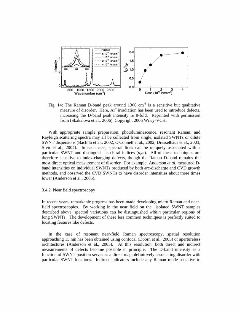
Fig. 14: The Raman D-band peak around 1300 cm-1 is a sensitive but qualitative measure of disorder. Here, Ar+ irradiation has been used to introduce defects, increasing the D-band peak intensity ID 8-fold. Reprinted with permission from (Skakalova et al., 2006). Copyright 2006 Wiley-VCH.
With appropriate sample preparation, photoluminescence, resonant Raman, and Rayleigh scattering spectra may all be collected from single, isolated SWNTs or dilute SWNT dispersions (Bachilo et al., 2002; O'Connell et al., 2002; Dresselhaus et al., 2003; Sfeir et al., 2004). In each case, spectral lines can be uniquely associated with a particular SWNT and distinguish its chiral indices (n,m). All of these techniques are therefore sensitive to index-changing defects, though the Raman D-band remains the most direct optical measurement of disorder. For example, Anderson et al. measured D-band intensities on individual SWNTs produced by both arc-discharge and CVD growth methods, and observed the CVD SWNTs to have disorder intensities about three times lower (Anderson et al., 2005).
3.4.2 Near field spectroscopy
In recent years, remarkable progress has been made developing micro Raman and near-field spectroscopies. By working in the near field on the isolated SWNT samples described above, spectral variations can be distinguished within particular regions of long SWNTs. The development of these less common techniques is perfectly suited to locating features like defects.
In the case of resonant near-field Raman spectroscopy, spatial resolution approaching 15 nm has been obtained using confocal (Doorn et al., 2005) or apertureless architectures (Anderson et al., 2005). At this resolution, both direct and indirect measurements of defects become possible in principle. The D-band intensity as a function of SWNT position serves as a direct map, definitively associating disorder with particular SWNT locations. Indirect indicators include any Raman mode sensitive to
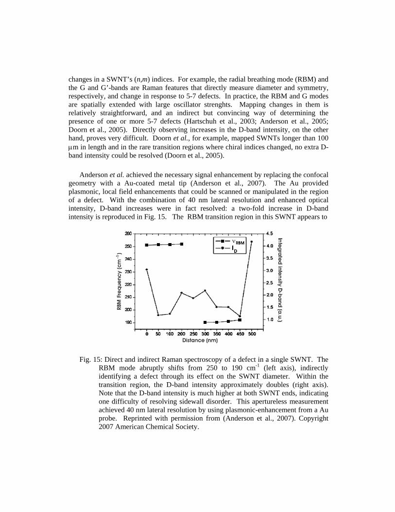
changes in a SWNT’s (n,m) indices. For example, the radial breathing mode (RBM) and the G and G’-bands are Raman features that directly measure diameter and symmetry, respectively, and change in response to 5-7 defects. In practice, the RBM and G modes are spatially extended with large oscillator strenghts. Mapping changes in them is relatively straightforward, and an indirect but convincing way of determining the presence of one or more 5-7 defects (Hartschuh et al., 2003; Anderson et al., 2005; Doorn et al., 2005). Directly observing increases in the D-band intensity, on the other hand, proves very difficult. Doorn et al., for example, mapped SWNTs longer than 100 μm in length and in the rare transition regions where chiral indices changed, no extra D-band intensity could be resolved (Doorn et al., 2005).
Anderson et al. achieved the necessary signal enhancement by replacing the confocal geometry with a Au-coated metal tip (Anderson et al., 2007). The Au provided plasmonic, local field enhancements that could be scanned or manipulated in the region of a defect. With the combination of 40 nm lateral resolution and enhanced optical intensity, D-band increases were in fact resolved: a two-fold increase in D-band intensity is reproduced in Fig. 15. The RBM transition region in this SWNT appears to
Fig. 15: Direct and indirect Raman spectroscopy of a defect in a single SWNT. The RBM mode abruptly shifts from 250 to 190 cm-1 (left axis), indirectly identifying a defect through its effect on the SWNT diameter. Within the transition region, the D-band intensity approximately doubles (right axis). Note that the D-band intensity is much higher at both SWNT ends, indicating one difficulty of resolving sidewall disorder. This apertureless measurement achieved 40 nm lateral resolution by using plasmonic-enhancement from a Au probe. Reprinted with permission from (Anderson et al., 2007). Copyright 2007 American Chemical Society.
extend over > 100 nm, suggesting perhaps two or more 5-7 defects separated by long distances. This particular arrangement may have aided the experiment, and further work will determine whether adjacent 5-7 defects and SW defects can be resolved in the D-band.
Whereas Raman spectra are sensitive to particular phonon modes, photoluminescence (PL) reflects the electronic bandstructure of a semiconducting SWNT (O'Connell et al., 2002; Bachilo et al., 2002) or MWNT (Uemura et al., 2006). Bandstructure is closely related to a SWNT’s (n,m) indices (Chou et al., 2004), so that a 5-7 defect that changes these indices can be mapped indirectly through its effect on electronic transitions, just as with the Raman RBM mode described above. In principle, a careful comparison of RBM and PL transitions surrounding a 5-7 defect might suggest different length scales, since the electronic and phonon localization lengths need not be identical. In practice, however, the interpretation of SWNT PL is much more complicated than a phonon map (Lefebvre et al., 2008). The primary source of PL in SWNTs is from radiative excitonic recombination. In the absence of disorder, SWNT excitons are relatively long-lived, diffusing over a 90 nm range and sampling approximately 10,000 lattice sites. The PL signal, then, is essentially a map of exciton diffusion and lifetime. Dilute disorder, whether from adsorbates, substrate charge traps, or lattice defects, amplifies nonradiative recombination channels and quenches this PL signal.
Finally, as near-field optics gets closer to resolving individual defects, it becomes possible to monitor defect creation in real time. In general, the Raman and PL techniques described above are sensitive to (n,m)-changing defects and not SW or vacancy defects that can be produced post-synthesis. Nevertheless, Cognet et al. studied the PL of individual SWNTs exposed to sulfuric acid or diazonium salts, and observed stepwise drops occuring during exposure (Cognet et al., 2007). The steps shown in Fig. 16 were attributed to the creation of adduct defects, much like conducance experiments to be described in Section 4.2. These adducts do not change the gross electronic spectrum of a SWNT, but they do pin excitons and amplify their nonradiative recombination channels. In similar work, defects have been observed to produce localized emission from unbound electron-hole pairs electrically injected from opposite ends of a SWNT (Freitag et al., 2006; Avouris et al., 2008).
3.5. Electrical conductance
Of the different methods for locating defects described in this Section, electrical conductance is probably the least well known outside the CNT field. Conductance is not generally sensitive to individual defects, and it is merely a measure of global disorder and doping in 3-D and bulk materials. This remains true as dimensionality is reduced to
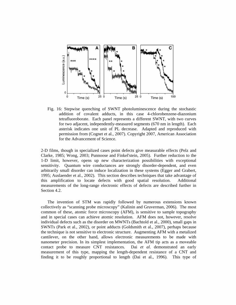
Fig. 16: Stepwise quenching of SWNT photoluminescence during the stochastic addition of covalent adducts, in this case 4-chlorobenzene-diazonium tetrafluoroborate. Each panel represents a different SWNT, with two curves for two adjacent, independently-measured segments (670 nm in length). Each asterisk indicates one unit of PL decrease. Adapted and reproduced with permission from (Cognet et al., 2007). Copyright 2007, American Association for the Advancement of Science.
2-D films, though in specialized cases point defects give measurable effects (Pelz and Clarke, 1985; Wong, 2003; Punnoose and Finkel'stein, 2005). Further reduction to the 1-D limit, however, opens up new characterization possibilities with exceptional sensitivity. Quantum wire conductances are strongly disorder-dependent, and even arbitrarily small disorder can induce localization in these systems (Egger and Grabert, 1995; Auslaender et al., 2002). This section describes techniques that take advantage of this amplification to locate defects with good spatial resolution. Additional measurements of the long-range electronic effects of defects are described further in Section 4.2.
The invention of STM was rapidly followed by numerous extensions known collectively as “scanning probe microscopy” (Kalinin and Gruverman, 2006). The most common of these, atomic force microscopy (AFM), is sensitive to sample topography and in special cases can achieve atomic resolution. AFM does not, however, resolve individual defects such as the disorder on MWNTs (Bachtold et al., 2000), small gaps in SWNTs (Park et al., 2002), or point adducts (Goldsmith et al., 2007), perhaps because the technique is not sensitive to electronic structure. Augmenting AFM with a metalized cantilever, on the other hand, allows electronic measurements to be made with nanometer precision. In its simplest implementation, the AFM tip acts as a moveable contact probe to measure CNT resistances. Dai et al. demonstrated an early measurement of this type, mapping the length-dependent resistance of a CNT and finding it to be roughly proportional to length (Dai et al., 1996). This type of
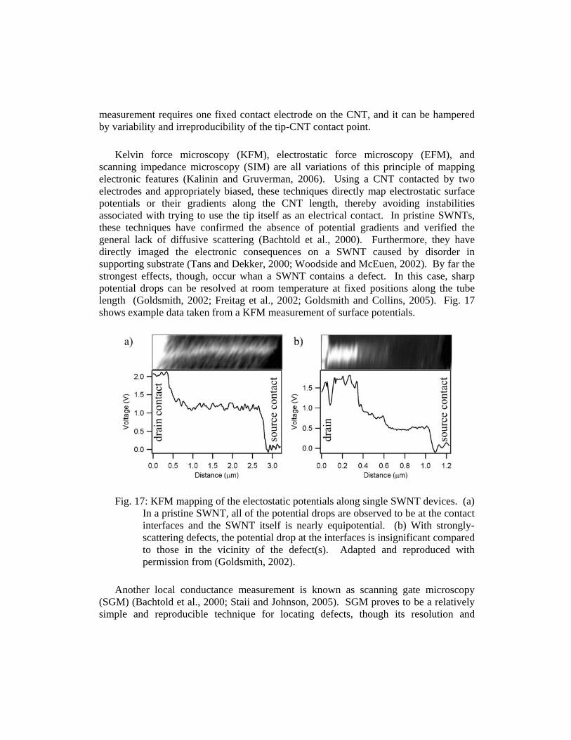
measurement requires one fixed contact electrode on the CNT, and it can be hampered by variability and irreproducibility of the tip-CNT contact point.
Kelvin force microscopy (KFM), electrostatic force microscopy (EFM), and scanning impedance microscopy (SIM) are all variations of this principle of mapping electronic features (Kalinin and Gruverman, 2006). Using a CNT contacted by two electrodes and appropriately biased, these techniques directly map electrostatic surface potentials or their gradients along the CNT length, thereby avoiding instabilities associated with trying to use the tip itself as an electrical contact. In pristine SWNTs, these techniques have confirmed the absence of potential gradients and verified the general lack of diffusive scattering (Bachtold et al., 2000). Furthermore, they have directly imaged the electronic consequences on a SWNT caused by disorder in supporting substrate (Tans and Dekker, 2000; Woodside and McEuen, 2002). By far the strongest effects, though, occur whan a SWNT contains a defect. In this case, sharp potential drops can be resolved at room temperature at fixed positions along the tube length (Goldsmith, 2002; Freitag et al., 2002; Goldsmith and Collins, 2005). Fig. 17 shows example data taken from a KFM measurement of surface potentials.
Fig. 17: KFM mapping of the electostatic potentials along single SWNT devices. (a) In a pristine SWNT, all of the potential drops are observed to be at the contact interfaces and the SWNT itself is nearly equipotential. (b) With strongly-scattering defects, the potential drop at the interfaces is insignificant compared to those in the vicinity of the defect(s). Adapted and reproduced with permission from (Goldsmith, 2002).
Another local conductance measurement is known as scanning gate microscopy (SGM) (Bachtold et al., 2000; Staii and Johnson, 2005). SGM proves to be a relatively simple and reproducible technique for locating defects, though its resolution and
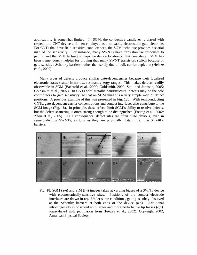
applicability is somewhat limited. In SGM, the conductive cantilever is biased with respect to a CNT device and then employed as a movable, electrostatic gate electrode. For CNTs that have field-sensitive conductances, the SGM technique provides a spatial map of the sensitivity. For instance, many SWNTs have transistor-like responses to gating, and the SGM technique maps the device location(s) that contribute. SGM has been tremendously helpful for proving that many SWNT transistors switch because of gate-sensitive Schottky barriers, rather than solely due to bulk carrier depletion (Heinze et al., 2002).
Many types of defects produce similar gate-dependencies because their localized electronic states scatter in narrow, resonant energy ranges. This makes defects readily observable in SGM (Bachtold et al., 2000; Goldsmith, 2002; Staii and Johnson, 2005; Goldsmith et al., 2007). In CNTs with metallic bandstructure, defects may be the sole contributors to gate sensitivity, so that an SGM image is a very simple map of defect positions. A previous example of this was presented in Fig. 12d. With semiconducting CNTs, gate-dependent carrier concentrations and contact interfaces also contribute to the SGM image (Fig. 18). In principle, these effects limit SGM’s ability to resolve defects, but the defect scattering is often strong enough to be distinguished (Freitag et al., 2002; Zhou et al., 2005). As a consequence, defect sites are often quite obvious, even in semiconducting SWNTs, as long as they are physically distant from the Schottky barriers.
Fig. 18: SGM (a-e) and SIM (f-j) images taken at varying biases of a SWNT device with electrostatically-sensitive sites. Positions of the contact electrode interfaces are drawn in (c). Under some conditions, gating is solely observed at the Schottky barriers at both ends of the device (a,b). Additional inhomogeneity is observed with larger and more perturbative tip biases (c,d). Reproduced with permission from (Freitag et al., 2002). Copyright 2002, American Physical Society.
The lateral resolution of these techniques rarely exceeds 20 nm, making them somewhat imprecise among the different scanning probe methods. However, they have the additional advantage of being able to perform electronic spectroscopies. The potential drop at a defect site is not simply proportional to the total bias applied to the CNT, but is instead energy dependent. Careful mapping of this dependence, which might reflect scattering processes that are resonant with the defect’s energy levels, may allow different types of defects to be electronically classified. This advance would be an important step for these techniques, because at present the structure of different defects reported by KFM or SGM has been decidedly vague. In fact, most measurements have been unable to distinguish between sidewall defects, adducts, and the more extrinsic effects discussed in Sec. 2.2: a charge trap in the CNT’s supporting oxide may locally enhance gate sensitivity as much as a SW defect. Differentiating between these possible mechanisms is key to the usefulness of the measurements, and energy-dependent mapping is a potential solution. Similar techniques have electronically distinguished different SWNT chiralities (Heo and Bockrath, 2005), but the application to defect spectroscopy remains unproven. Ultimately, different defect types may be too similar to be distinguished (Orlikowski et al., 2000).
Mobile surface contaminants present substantial difficulties to the techniques described here. In ambient conditions, these contaminants dynamically follow the scanning probe and screen its effectiveness (Kalinin and Bonnell, 2004). More accurate electronic information is recovered by performing measurements in UHV conditions, but with a low throughput that undermines the effectiveness of the techniques for locating defects. Furthermore, sample preparations like baking and degassing possibly modify a defect’s interesting aspects. An intermediate solution to UHV is to cool samples below 0 oC for imaging. Rather than removing all surface ions, cooling fixes the ions in place by freezing the surface moisture that contributes to their high mobility. Comparison of images taken at 20 oC and -70 oC indicate virtually no change in electrical characteristics, despite substantial contrast enhancements in EFM, KFM, and SGM.
4. PHYSICAL CONSEQUENCES OF DEFECTS AND DISORDER
The final main Section of this chapter focuses on the long-range consequences of defects and disorder. Of course, some of the physical consequences of defects are the enabling mechanisms for the experimental methods just described, and every CNT defect of course has its individual, localized effects. This Section focuses on additional effects that, while not used primarily as methods for locating defects, are nonetheless sensitive to their presence.
In particular, a single defect can be consequential far out of proportion to its atomic
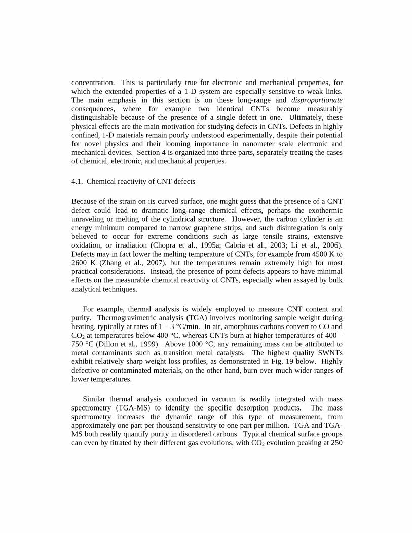
concentration. This is particularly true for electronic and mechanical properties, for which the extended properties of a 1-D system are especially sensitive to weak links. The main emphasis in this section is on these long-range and disproportionate consequences, where for example two identical CNTs become measurably distinguishable because of the presence of a single defect in one. Ultimately, these physical effects are the main motivation for studying defects in CNTs. Defects in highly confined, 1-D materials remain poorly understood experimentally, despite their potential for novel physics and their looming importance in nanometer scale electronic and mechanical devices. Section 4 is organized into three parts, separately treating the cases of chemical, electronic, and mechanical properties.
4.1. Chemical reactivity of CNT defects
Because of the strain on its curved surface, one might guess that the presence of a CNT defect could lead to dramatic long-range chemical effects, perhaps the exothermic unraveling or melting of the cylindrical structure. However, the carbon cylinder is an energy minimum compared to narrow graphene strips, and such disintegration is only believed to occur for extreme conditions such as large tensile strains, extensive oxidation, or irradiation (Chopra et al., 1995a; Cabria et al., 2003; Li et al., 2006). Defects may in fact lower the melting temperature of CNTs, for example from 4500 K to 2600 K (Zhang et al., 2007), but the temperatures remain extremely high for most practical considerations. Instead, the presence of point defects appears to have minimal effects on the measurable chemical reactivity of CNTs, especially when assayed by bulk analytical techniques.
For example, thermal analysis is widely employed to measure CNT content and purity. Thermogravimetric analysis (TGA) involves monitoring sample weight during heating, typically at rates of 1 – 3 °C/min. In air, amorphous carbons convert to CO and CO2 at temperatures below 400 °C, whereas CNTs burn at higher temperatures of 400 – 750 °C (Dillon et al., 1999). Above 1000 °C, any remaining mass can be attributed to metal contaminants such as transition metal catalysts. The highest quality SWNTs exhibit relatively sharp weight loss profiles, as demonstrated in Fig. 19 below. Highly defective or contaminated materials, on the other hand, burn over much wider ranges of lower temperatures.
Similar thermal analysis conducted in vacuum is readily integrated with mass spectrometry (TGA-MS) to identify the specific desorption products. The mass spectrometry increases the dynamic range of this type of measurement, from approximately one part per thousand sensitivity to one part per million. TGA and TGA-MS both readily quantify purity in disordered carbons. Typical chemical surface groups can even by titrated by their different gas evolutions, with CO2 evolution peaking at 250
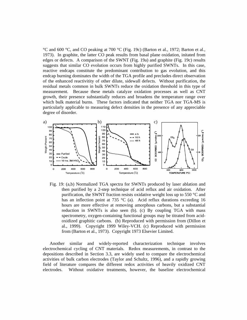
°C and 600 °C, and CO peaking at 700 °C (Fig. 19c) (Barton et al., 1972; Barton et al., 1973). In graphite, the latter CO peak results from basal plane oxidation, initated from edges or defects. A comparison of the SWNT (Fig. 19a) and graphite (Fig. 19c) results suggests that similar CO evolution occurs from highly purified SWNTs. In this case, reactive endcaps constitute the predominant contribution to gas evolution, and this endcap burning dominates the width of the TGA profile and precludes direct observation of the enhanced reactivitity of other dilute, sidewall defects. Without purification, the residual metals common in bulk SWNTs reduce the oxidation threshold in this type of measurement. Because these metals catalyze oxidation processes as well as CNT growth, their presence substantially reduces and broadens the temperature range over which bulk material burns. These factors indicated that neither TGA nor TGA-MS is particularly applicable to measuring defect densities in the presence of any appreciable degree of disorder.
Fig. 19: (a,b) Normalized TGA spectra for SWNTs produced by laser ablation and then purified by a 2-step technique of acid reflux and air oxidation. After purification, the SWNT fraction resists oxidative weight loss up to 550 °C and has an inflection point at 735 °C (a). Acid reflux durations exceeding 16 hours are more effective at removing amorphous carbons, but a substantial reduction in SWNTs is also seen (b). (c) By coupling TGA with mass spectrometry, oxygen-containing functional groups may be titrated from acid-oxidized graphitic carbons. (b) Reproduced with permission from (Dillon et al., 1999). Copyright 1999 Wiley-VCH. (c) Reproduced with permission from (Barton et al., 1973). Copyright 1973 Elsevier Limited.
Another similar and widely-reported characterization technique involves electrochemical cycling of CNT materials. Redox measurements, in contrast to the depositions described in Section 3.3, are widely used to compare the electrochemical activities of bulk carbon electrodes (Taylor and Schultz, 1996), and a rapidly growing field of literature compares the different redox activities of heavily oxidized CNT electrodes. Without oxidative treatments, however, the baseline electrochemical
a) b) c)
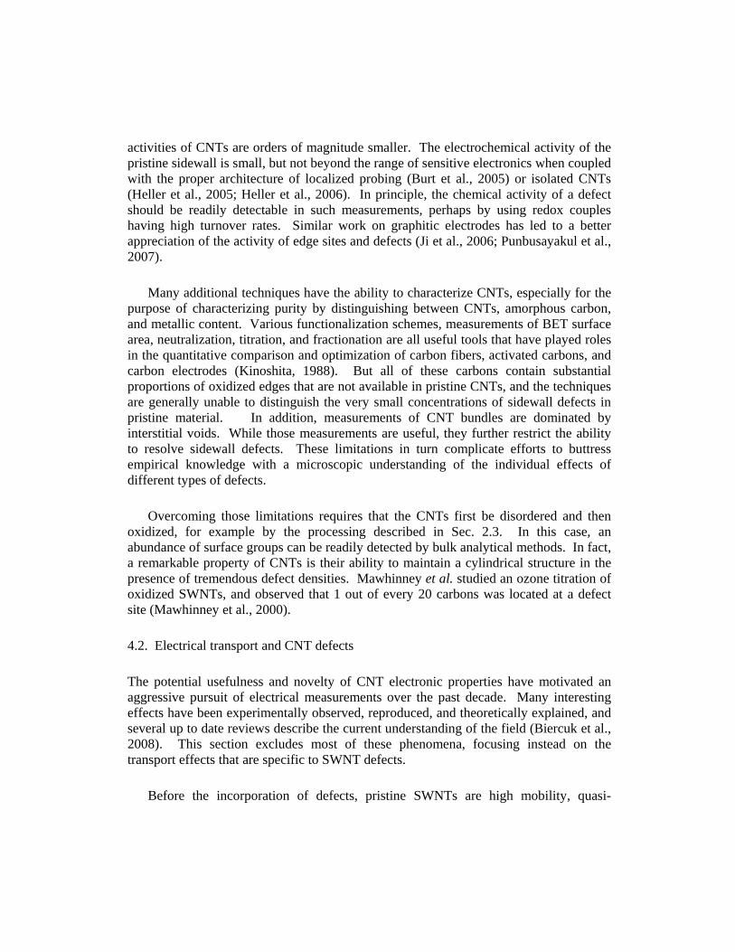
activities of CNTs are orders of magnitude smaller. The electrochemical activity of the pristine sidewall is small, but not beyond the range of sensitive electronics when coupled with the proper architecture of localized probing (Burt et al., 2005) or isolated CNTs (Heller et al., 2005; Heller et al., 2006). In principle, the chemical activity of a defect should be readily detectable in such measurements, perhaps by using redox couples having high turnover rates. Similar work on graphitic electrodes has led to a better appreciation of the activity of edge sites and defects (Ji et al., 2006; Punbusayakul et al., 2007).
Many additional techniques have the ability to characterize CNTs, especially for the purpose of characterizing purity by distinguishing between CNTs, amorphous carbon, and metallic content. Various functionalization schemes, measurements of BET surface area, neutralization, titration, and fractionation are all useful tools that have played roles in the quantitative comparison and optimization of carbon fibers, activated carbons, and carbon electrodes (Kinoshita, 1988). But all of these carbons contain substantial proportions of oxidized edges that are not available in pristine CNTs, and the techniques are generally unable to distinguish the very small concentrations of sidewall defects in pristine material. In addition, measurements of CNT bundles are dominated by interstitial voids. While those measurements are useful, they further restrict the ability to resolve sidewall defects. These limitations in turn complicate efforts to buttress empirical knowledge with a microscopic understanding of the individual effects of different types of defects.
Overcoming those limitations requires that the CNTs first be disordered and then oxidized, for example by the processing described in Sec. 2.3. In this case, an abundance of surface groups can be readily detected by bulk analytical methods. In fact, a remarkable property of CNTs is their ability to maintain a cylindrical structure in the presence of tremendous defect densities. Mawhinney et al. studied an ozone titration of oxidized SWNTs, and observed that 1 out of every 20 carbons was located at a defect site (Mawhinney et al., 2000).
4.2. Electrical transport and CNT defects
The potential usefulness and novelty of CNT electronic properties have motivated an aggressive pursuit of electrical measurements over the past decade. Many interesting effects have been experimentally observed, reproduced, and theoretically explained, and several up to date reviews describe the current understanding of the field (Biercuk et al., 2008). This section excludes most of these phenomena, focusing instead on the transport effects that are specific to SWNT defects.
Before the incorporation of defects, pristine SWNTs are high mobility, quasi-
ballistic conductors with exceptional properties. The SWNT conductance G is often discussed in terms of the quantum of conductance, Go = 2e2/h, appropriate for a single, current-carrying, 1-D channel or quantum state with spin degeneracy. The pristine, metallic SWNT has two such states, located at the K and K’ momentum points of graphene’s Brillouin zone. Mixing between these states, as well as electron-phonon scattering and backscattering generally, is strongly suppressed (McEuen et al., 1999; Ando, 2005), so that short, clean SWNTs behave like ballistic, 1-D conductors.
4.2.1 Conductance of topology-changing 5-7 defects
Before the first SWNT devices had been successfully fabricated or measured, the possibility of novel SWNT heterojunctions had been considered theoretically (Charlier et al., 1996; Chico et al., 1996b; Chico et al., 1996a; Saito et al., 1996). These “junctions,” described above in Sections 2.1 and 3.1, consist of SWNTs with 5-7 defects that change the topological indices (n,m) midway along the SWNT. Because electronic bandstructure is sensitive to these indices in SWNTs, this type of defect is remarkably consequential. As confirmed by STM spectroscopy (Ouyang et al., 2001; Kim et al., 2003a; Ishigami et al., 2004), different defect configurations can change semiconducting SWNTs into metallic ones and vice versa, thereby producing 1-D semiconductor-semiconductor, metal-semiconductor, and metal-metal heterojunctions depicted in Fig. 20.
While these junctions can be atomically resolved on metallic surfaces, testing their transport properties requires an insulating substrate that precludes STM imaging. Nevertheless, certain defect configurations result in characteristic kinks, and these kinks are easily resolved by AFM. Yao et al. found approximately 1% of 500 SWNT devices to contain sharp kinks, and proceeded to electrically characterize these (Yao et al., 1999). Some kinks exhibited asymmetric rectification appropriate for metal-semiconductor junctions (Fig. 20d). Other, more conductive devices had nonlinear I-V characteristics and temperature dependences suggestive of metal-insulator-metal junctions. In both types, the transport is dominated by a tunneling barrier formed at the heterojunction interface, i.e. by localized states surrounding the defect site(s). Yao et al. analyzed their results in terms of tunneling between Luttinger liquids, an aspect of SWNT junctions that is wholly different from conventional 2-D heterojunctions. Unfortunately, due to both the rarity of such devices and the lack of precise indexing, there has been limited opportunity to model the particular characteristics of specific atomic arrangements. Recent progress indexing junctions optically, as described in Section 3.4b, combined with the deterministic synthesis of heterojunctions described in Section 2.1c, should lead to renewed activity and progress in this area.
Other notable cases of rectification have been observed in different SWNT junctions.
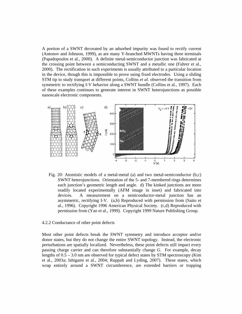
A portion of a SWNT decorated by an adsorbed impurity was found to rectify current (Antonov and Johnson, 1999), as are many Y-branched MWNTs having three terminals (Papadopoulos et al., 2000). A definite metal-semiconductor junction was fabricated at the crossing point between a semiconducting SWNT and a metallic one (Fuhrer et al., 2000). The rectification in such experiments is usually attributed to a particular location in the device, though this is impossible to prove using fixed electrodes. Using a sliding STM tip to study transport at different points, Collins et al. observed the transition from symmetric to rectifying I-V behavior along a SWNT bundle (Collins et al., 1997). Each of these examples continues to generate interest in SWNT heterojunctions as possible nanoscale electronic components.
Fig. 20: Atomistic models of a metal-metal (a) and two metal-semiconductor (b,c) SWNT heterojunctions. Orientation of the 5- and 7-membered rings determines each junction’s geometric length and angle. d) The kinked junctions are more readily located experimentally (AFM image in inset) and fabricated into devices. A measurement on a semiconductor-metal junction has an asymmetric, rectifying I-V. (a,b) Reproduced with permission from (Saito et al., 1996). Copyright 1996 American Physical Society. (c,d) Reproduced with permission from (Yao et al., 1999). Copyright 1999 Nature Publishing Group.
4.2.2 Conductance of other point defects
Most other point defects break the SWNT symmetry and introduce acceptor and/or donor states, but they do not change the entire SWNT topology. Instead, the electronic perturbations are spatially localized. Nevertheless, these point defects still impact every passing charge carrier and can therefore substantially change G. For example, decay lengths of 0.5 – 3.0 nm are observed for typical defect states by STM spectroscopy (Kim et al., 2003a; Ishigami et al., 2004; Ruppalt and Lyding, 2007). These states, which wrap entirely around a SWNT circumference, are extended barriers or trapping
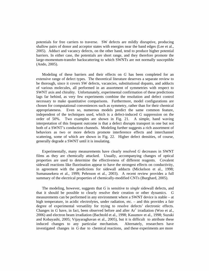
potentials for free carriers to traverse. SW defects are mildly disruptive, producing shallow pairs of donor and acceptor states with energies near the band edges (Lee et al., 2005). Adduct and vacancy defects, on the other hand, tend to produce higher potential barriers. In either case, the potentials are short range, and they therefore promote the large-momentum-transfer backscattering to which SWNTs are not normally susceptible (Ando, 2005).
Modeling of these barriers and their effects on G has been completed for an extensive range of defect types. The theoretical literature deserves a separate review to be thorough, since it covers SW defects, vacancies, substitutional dopants, and adducts of various molecules, all performed in an assortment of symmetries with respect to SWNT axis and chirality. Unfortunately, experimental confirmation of these predictions lags far behind, as very few experiments combine the resolution and defect control necessary to make quantitative comparisons. Furthermore, model configurations are chosen for computational conveniences such as symmetry, rather than for their chemical appropriateness. Even so, numerous models predict the same common feature, independent of the techniques used, which is a defect-induced G suppression on the order of 50%. Two examples are shown in Fig. 21. A simple, hand waving interpretation of this frequent outcome is that a defect disrupts transport in one but not both of a SWNT’s conduction channels. Modeling further suggests a rich assortment of behaviors as two or more defects promote interference effects and interchannel scattering, some of which are shown in Fig. 22. Higher defect densities, of course, generally degrade a SWNT until it is insulating.
Experimentally, many measurements have clearly resolved G decreases in SWNT films as they are chemically attacked. Usually, accompanying changes of optical properties are used to determine the effectiveness of different reagents. Covalent sidewall reactions like fluorination appear to have the strongest effects on conductivity, in agreement with the predictions for sidewall adducts (Mickelson et al., 1998; Sumanasekera et al., 1999; Pehrsson et al., 2003). A recent review provides a full summary of the electrical properties of chemically-modified CNTs (Burghard, 2005).
The modeling, however, suggests that G is sensitive to single sidewall defects, and that it should be possible to clearly resolve their creation or other dynamics. G measurements can be performed in any environment where a SWNT device is stable – at high temperature, in acidic electrolytes, under radiation, etc. – and this provides a fair degree of experimental versatility for trying to resolve defects’ electronic effects. Changes in G have, in fact, been observed before and after Ar+ irradiation (Woo et al., 2006) and electron beam irradiation (Bachtold et al., 1998; Kasumov et al., 1998; Suzuki and Kobayashi, 2005; Vijayaraghavan et al., 2005), but it is difficult to attribute these induced changes to any particular mechanism. Alternately, researchers have investigated changes in G due to chemical reactions, and these experiments are more
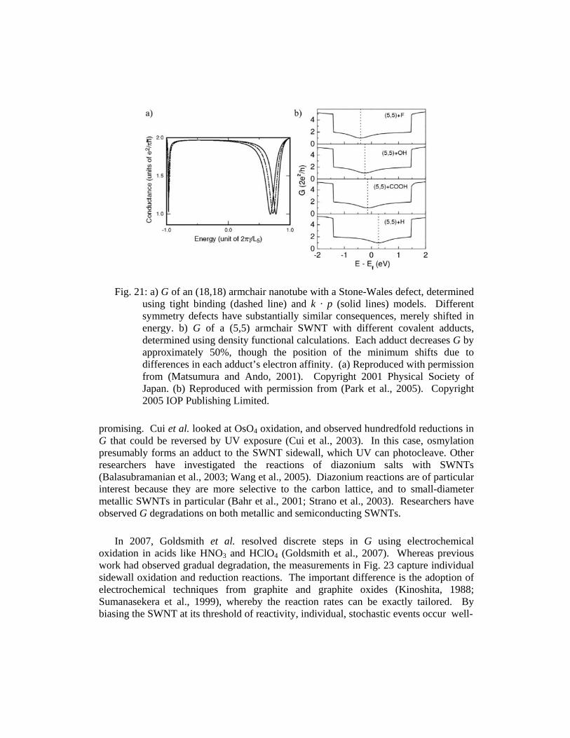
Fig. 21: a) G of an (18,18) armchair nanotube with a Stone-Wales defect, determined using tight binding (dashed line) and k · p (solid lines) models. Different symmetry defects have substantially similar consequences, merely shifted in energy. b) G of a (5,5) armchair SWNT with different covalent adducts, determined using density functional calculations. Each adduct decreases G by approximately 50%, though the position of the minimum shifts due to differences in each adduct’s electron affinity. (a) Reproduced with permission from (Matsumura and Ando, 2001). Copyright 2001 Physical Society of Japan. (b) Reproduced with permission from (Park et al., 2005). Copyright 2005 IOP Publishing Limited.
promising. Cui et al. looked at OsO4 oxidation, and observed hundredfold reductions in G that could be reversed by UV exposure (Cui et al., 2003). In this case, osmylation presumably forms an adduct to the SWNT sidewall, which UV can photocleave. Other researchers have investigated the reactions of diazonium salts with SWNTs (Balasubramanian et al., 2003; Wang et al., 2005). Diazonium reactions are of particular interest because they are more selective to the carbon lattice, and to small-diameter metallic SWNTs in particular (Bahr et al., 2001; Strano et al., 2003). Researchers have observed G degradations on both metallic and semiconducting SWNTs.
In 2007, Goldsmith et al. resolved discrete steps in G using electrochemical oxidation in acids like HNO3 and HClO4 (Goldsmith et al., 2007). Whereas previous work had observed gradual degradation, the measurements in Fig. 23 capture individual sidewall oxidation and reduction reactions. The important difference is the adoption of electrochemical techniques from graphite and graphite oxides (Kinoshita, 1988; Sumanasekera et al., 1999), whereby the reaction rates can be exactly tailored. By biasing the SWNT at its threshold of reactivity, individual, stochastic events occur well-
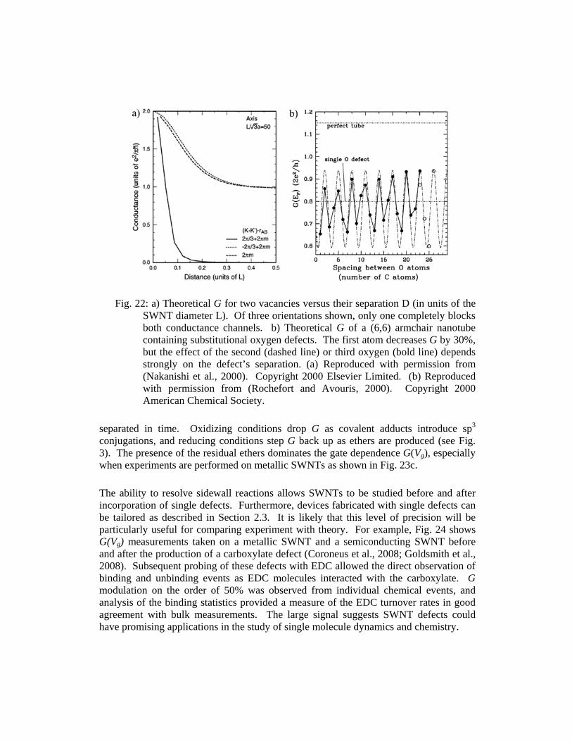
Fig. 22: a) Theoretical G for two vacancies versus their separation D (in units of the SWNT diameter L). Of three orientations shown, only one completely blocks both conductance channels. b) Theoretical G of a (6,6) armchair nanotube containing substitutional oxygen defects. The first atom decreases G by 30%, but the effect of the second (dashed line) or third oxygen (bold line) depends strongly on the defect’s separation. (a) Reproduced with permission from (Nakanishi et al., 2000). Copyright 2000 Elsevier Limited. (b) Reproduced with permission from (Rochefort and Avouris, 2000). Copyright 2000 American Chemical Society.
separated in time. Oxidizing conditions drop G as covalent adducts introduce sp3 conjugations, and reducing conditions step G back up as ethers are produced (see Fig. 3). The presence of the residual ethers dominates the gate dependence G(Vg), especially when experiments are performed on metallic SWNTs as shown in Fig. 23c.
The ability to resolve sidewall reactions allows SWNTs to be studied before and after incorporation of single defects. Furthermore, devices fabricated with single defects can be tailored as described in Section 2.3. It is likely that this level of precision will be particularly useful for comparing experiment with theory. For example, Fig. 24 shows G(Vg) measurements taken on a metallic SWNT and a semiconducting SWNT before and after the production of a carboxylate defect (Coroneus et al., 2008; Goldsmith et al., 2008). Subsequent probing of these defects with EDC allowed the direct observation of binding and unbinding events as EDC molecules interacted with the carboxylate. G modulation on the order of 50% was observed from individual chemical events, and analysis of the binding statistics provided a measure of the EDC turnover rates in good agreement with bulk measurements. The large signal suggests SWNT defects could have promising applications in the study of single molecule dynamics and chemistry.
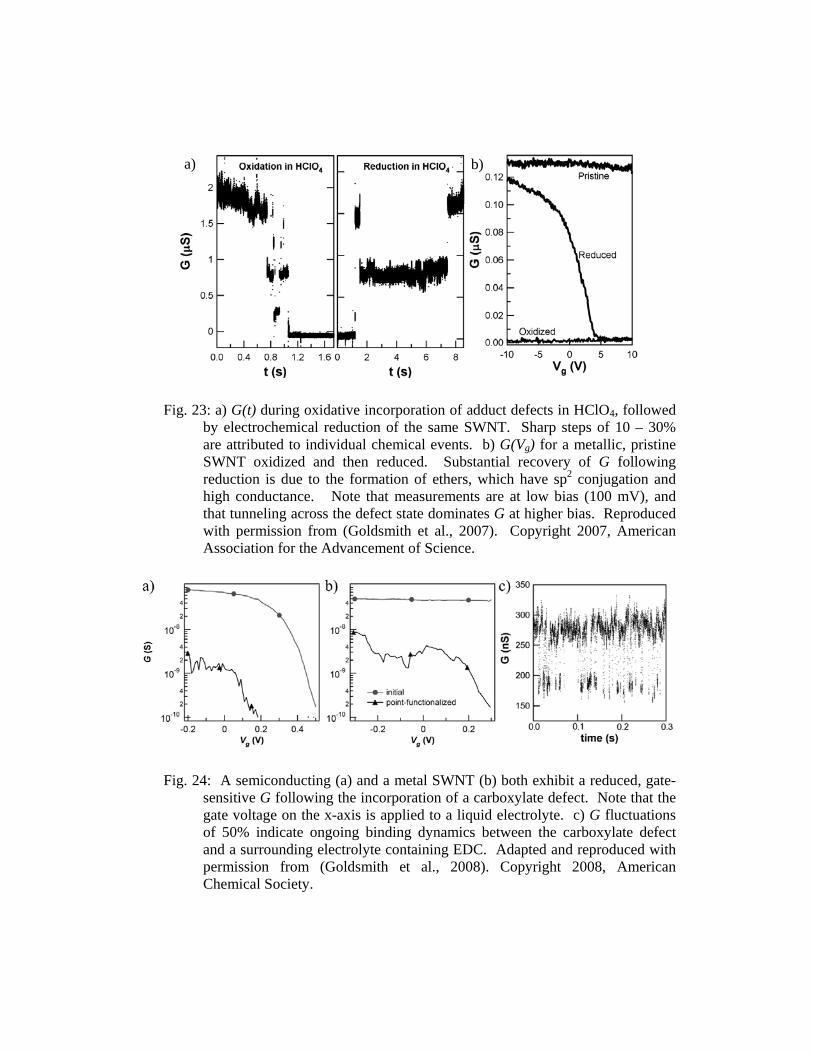
Fig. 23: a) G(t) during oxidative incorporation of adduct defects in HClO4, followed by electrochemical reduction of the same SWNT. Sharp steps of 10 – 30% are attributed to individual chemical events. b) G(Vg) for a metallic, pristine SWNT oxidized and then reduced. Substantial recovery of G following reduction is due to the formation of ethers, which have sp2 conjugation and high conductance. Note that measurements are at low bias (100 mV), and that tunneling across the defect state dominates G at higher bias. Reproduced with permission from (Goldsmith et al., 2007). Copyright 2007, American Association for the Advancement of Science.
Fig. 24: A semiconducting (a) and a metal SWNT (b) both exhibit a reduced, gate-sensitive G following the incorporation of a carboxylate defect. Note that the gate voltage on the x-axis is applied to a liquid electrolyte. c) G fluctuations of 50% indicate ongoing binding dynamics between the carboxylate defect and a surrounding electrolyte containing EDC. Adapted and reproduced with permission from (Goldsmith et al., 2008). Copyright 2008, American Chemical Society.
a) b)
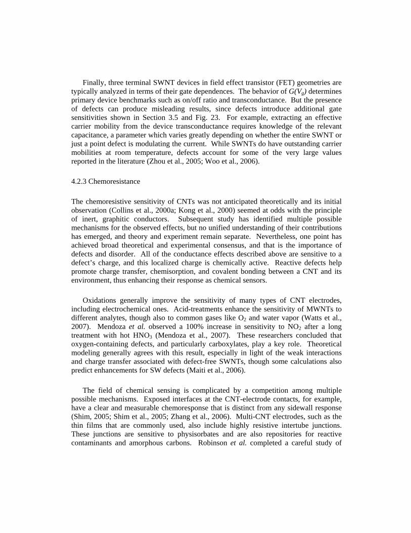
Finally, three terminal SWNT devices in field effect transistor (FET) geometries are typically analyzed in terms of their gate dependences. The behavior of G(Vg) determines primary device benchmarks such as on/off ratio and transconductance. But the presence of defects can produce misleading results, since defects introduce additional gate sensitivities shown in Section 3.5 and Fig. 23. For example, extracting an effective carrier mobility from the device transconductance requires knowledge of the relevant capacitance, a parameter which varies greatly depending on whether the entire SWNT or just a point defect is modulating the current. While SWNTs do have outstanding carrier mobilities at room temperature, defects account for some of the very large values reported in the literature (Zhou et al., 2005; Woo et al., 2006).
4.2.3 Chemoresistance
The chemoresistive sensitivity of CNTs was not anticipated theoretically and its initial observation (Collins et al., 2000a; Kong et al., 2000) seemed at odds with the principle of inert, graphitic conductors. Subsequent study has identified multiple possible mechanisms for the observed effects, but no unified understanding of their contributions has emerged, and theory and experiment remain separate. Nevertheless, one point has achieved broad theoretical and experimental consensus, and that is the importance of defects and disorder. All of the conductance effects described above are sensitive to a defect’s charge, and this localized charge is chemically active. Reactive defects help promote charge transfer, chemisorption, and covalent bonding between a CNT and its environment, thus enhancing their response as chemical sensors.
Oxidations generally improve the sensitivity of many types of CNT electrodes, including electrochemical ones. Acid-treatments enhance the sensitivity of MWNTs to different analytes, though also to common gases like O2 and water vapor (Watts et al., 2007). Mendoza et al. observed a 100% increase in sensitivity to NO2 after a long treatment with hot HNO3 (Mendoza et al., 2007). These researchers concluded that oxygen-containing defects, and particularly carboxylates, play a key role. Theoretical modeling generally agrees with this result, especially in light of the weak interactions and charge transfer associated with defect-free SWNTs, though some calculations also predict enhancements for SW defects (Maiti et al., 2006).
The field of chemical sensing is complicated by a competition among multiple possible mechanisms. Exposed interfaces at the CNT-electrode contacts, for example, have a clear and measurable chemoresponse that is distinct from any sidewall response (Shim, 2005; Shim et al., 2005; Zhang et al., 2006). Multi-CNT electrodes, such as the thin films that are commonly used, also include highly resistive intertube junctions. These junctions are sensitive to physisorbates and are also repositories for reactive contaminants and amorphous carbons. Robinson et al. completed a careful study of
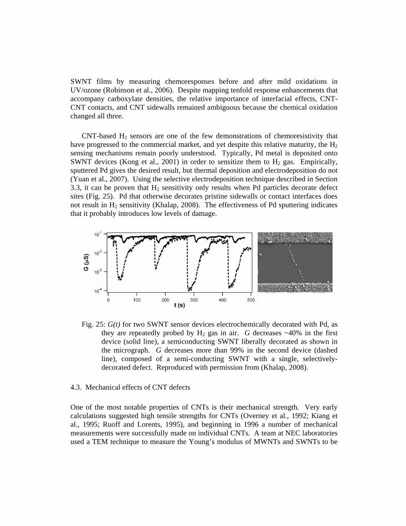
SWNT films by measuring chemoresponses before and after mild oxidations in UV/ozone (Robinson et al., 2006). Despite mapping tenfold response enhancements that accompany carboxylate densities, the relative importance of interfacial effects, CNT-CNT contacts, and CNT sidewalls remained ambiguous because the chemical oxidation changed all three.
CNT-based H2 sensors are one of the few demonstrations of chemoresistivity that have progressed to the commercial market, and yet despite this relative maturity, the H2 sensing mechanisms remain poorly understood. Typically, Pd metal is deposited onto SWNT devices (Kong et al., 2001) in order to sensitize them to H2 gas. Empirically, sputtered Pd gives the desired result, but thermal deposition and electrodeposition do not (Yuan et al., 2007). Using the selective electrodeposition technique described in Section 3.3, it can be proven that H2 sensitivity only results when Pd particles decorate defect sites (Fig. 25). Pd that otherwise decorates pristine sidewalls or contact interfaces does not result in H2 sensitivity (Khalap, 2008). The effectiveness of Pd sputtering indicates that it probably introduces low levels of damage.
Fig. 25: G(t) for two SWNT sensor devices electrochemically decorated with Pd, as they are repeatedly probed by H2 gas in air. G decreases ~40% in the first device (solid line), a semiconducting SWNT liberally decorated as shown in the micrograph. G decreases more than 99% in the second device (dashed line), composed of a semi-conducting SWNT with a single, selectively-decorated defect. Reproduced with permission from (Khalap, 2008).
4.3. Mechanical effects of CNT defects
One of the most notable properties of CNTs is their mechanical strength. Very early calculations suggested high tensile strengths for CNTs (Overney et al., 1992; Kiang et al., 1995; Ruoff and Lorents, 1995), and beginning in 1996 a number of mechanical measurements were successfully made on individual CNTs. A team at NEC laboratories used a TEM technique to measure the Young’s modulus of MWNTs and SWNTs to be
approximately 2 TPa and 1.2 TPa, respectively (Treacy et al., 1996; Krishnan et al., 1998). Similar values were obtained independently using AFM techniques (Wong et al., 1997; Falvo et al., 1997). Subsequently, a variety of strength measurements have been performed on individual CNTs, bundles and yarns of CNTs, and CNTs incorporated into composites. In general, the tensile strength of CNT ropes can exceed 1 GPa and withstand strains of 5% or more. These high values, combined with outstanding strength-to-weight ratios, make CNTs technically superior to metal alloys, Kevlar, or other carbon-based polymers (Baughman et al., 2002), and have even supported speculation about cabling for Earthbound space elevators.
Obviously, this extraordinary mechanical strength is sensitive to defect densities, but it is important not to overemphasize their role. Many factors limit the ultimate performance of high performance fibers, and the presence or absence of CNT defects is only relevant in the limit that no other weaknesses exist. Experimental fibers may contain voids, inhomogeneous microstructure, and CNTs weakened by kinks, entanglements, and twists. Furthermore, mechanical testing on macroscopic samples require efficient strain transfer from one CNT to another, and early mechanical experiments routinely observed CNTs pulling out of their matrices rather than tearing (Ajayan et al., 1994). To address these failure modes, researchers have actively pursued chemical oxidation and functionalization to provide covalent linkages, either among the CNTs or between them and a supporting matrix. The relatively inert CNT surfaces are poorly suited to covalent intertube strengthening, though, and the net effect of these treatments has usually been to compromise the intrinsic strength of the CNT lattice. Much of the existing literature therefore places lower bounds on the actual strain or strength of individual CNTs, and in the context of such difficulties the consequences of dilute defects are completely obscured.
Defects like di-vacancies and interstitials are mechanically important in graphites and graphitic carbon fibers because they help to form interlayer bonds among the carbon sheets. Similar crosslinks increase the shear strength of MWNTs and can reduce the “sword-in-sheath” failure in which the core of a MWNT pulls out of an outer shell (Cumings and Zettl, 2000; Yu et al., 2000c; Deshpande et al., 2006). Crosslinking interstitials also seem to play a role in intertube welding or coalescence (Terrones et al., 2000; Krasheninnikov et al., 2002b; Terrones et al., 2002b). However, as described previously, such defects are not thermodynamically likely in pristine material. Instead, they usually result from intentional modifications, such as those that serve to weaken the CNTs but effectively bind them within a matrix. This type of disorder, including surface functionalization, is treated in more detail by Hauke and Graupner in this Handbook.
Despite these problems, progress has been made preparing high quality fibers from CNTs. Their fabrication, testing and optimization has progressed rapidly by adopting technologies like spinning and extrusion from the mature industries of carbon and
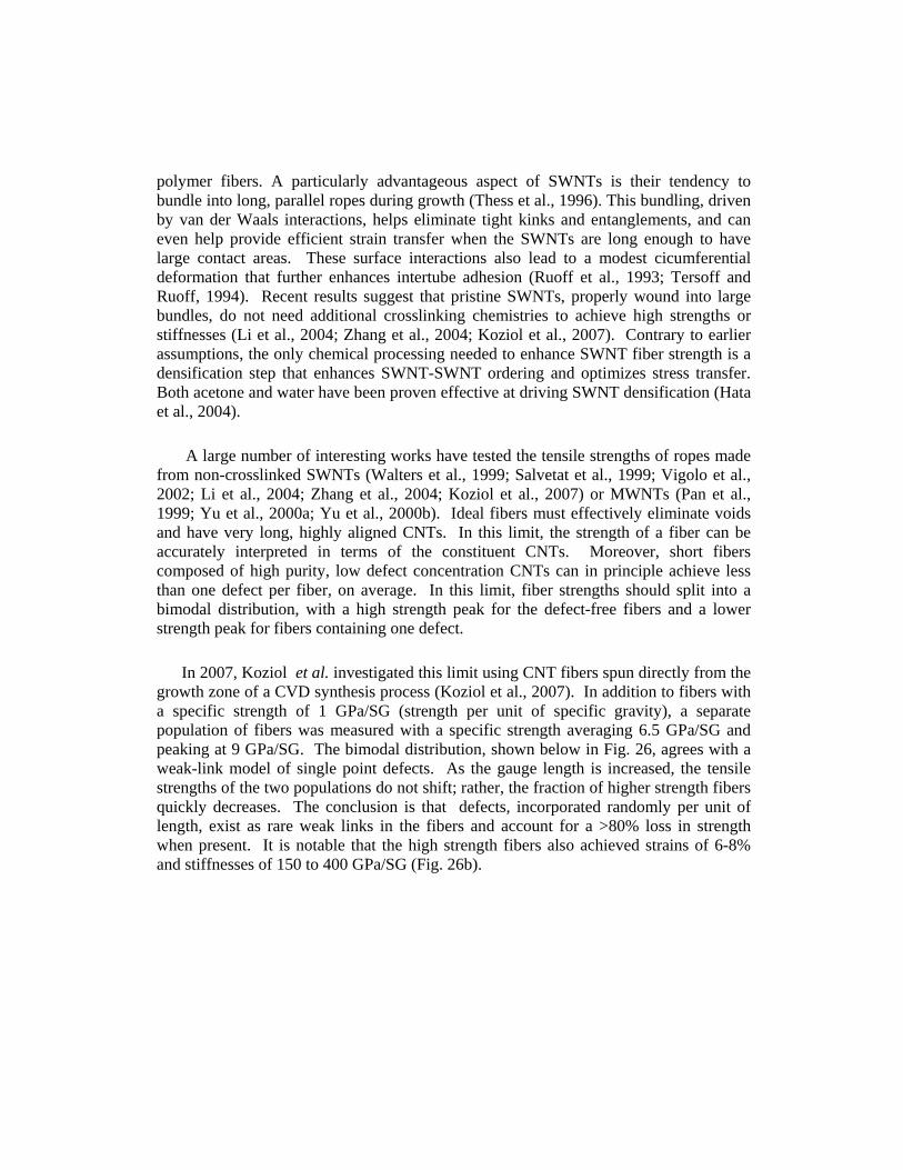
polymer fibers. A particularly advantageous aspect of SWNTs is their tendency to bundle into long, parallel ropes during growth (Thess et al., 1996). This bundling, driven by van der Waals interactions, helps eliminate tight kinks and entanglements, and can even help provide efficient strain transfer when the SWNTs are long enough to have large contact areas. These surface interactions also lead to a modest cicumferential deformation that further enhances intertube adhesion (Ruoff et al., 1993; Tersoff and Ruoff, 1994). Recent results suggest that pristine SWNTs, properly wound into large bundles, do not need additional crosslinking chemistries to achieve high strengths or stiffnesses (Li et al., 2004; Zhang et al., 2004; Koziol et al., 2007). Contrary to earlier assumptions, the only chemical processing needed to enhance SWNT fiber strength is a densification step that enhances SWNT-SWNT ordering and optimizes stress transfer. Both acetone and water have been proven effective at driving SWNT densification (Hata et al., 2004).
A large number of interesting works have tested the tensile strengths of ropes made from non-crosslinked SWNTs (Walters et al., 1999; Salvetat et al., 1999; Vigolo et al., 2002; Li et al., 2004; Zhang et al., 2004; Koziol et al., 2007) or MWNTs (Pan et al., 1999; Yu et al., 2000a; Yu et al., 2000b). Ideal fibers must effectively eliminate voids and have very long, highly aligned CNTs. In this limit, the strength of a fiber can be accurately interpreted in terms of the constituent CNTs. Moreover, short fibers composed of high purity, low defect concentration CNTs can in principle achieve less than one defect per fiber, on average. In this limit, fiber strengths should split into a bimodal distribution, with a high strength peak for the defect-free fibers and a lower strength peak for fibers containing one defect.
In 2007, Koziol et al. investigated this limit using CNT fibers spun directly from the growth zone of a CVD synthesis process (Koziol et al., 2007). In addition to fibers with a specific strength of 1 GPa/SG (strength per unit of specific gravity), a separate population of fibers was measured with a specific strength averaging 6.5 GPa/SG and peaking at 9 GPa/SG. The bimodal distribution, shown below in Fig. 26, agrees with a weak-link model of single point defects. As the gauge length is increased, the tensile strengths of the two populations do not shift; rather, the fraction of higher strength fibers quickly decreases. The conclusion is that defects, incorporated randomly per unit of length, exist as rare weak links in the fibers and account for a >80% loss in strength when present. It is notable that the high strength fibers also achieved strains of 6-8% and stiffnesses of 150 to 400 GPa/SG (Fig. 26b).
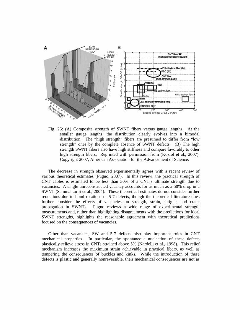
Fig. 26: (A) Composite strength of SWNT fibers versus gauge lengths. At the smaller gauge lengths, the distribution clearly evolves into a bimodal distribution. The “high strength” fibers are presumed to differ from “low strength” ones by the complete absence of SWNT defects. (B) The high strength SWNT fibers also have high stiffness and compare favorably to other high strength fibers. Reprinted with permission from (Koziol et al., 2007). Copyright 2007, American Association for the Advancement of Science.
The decrease in strength observed experimentally agrees with a recent review of various theoretical estimates (Pugno, 2007). In this review, the practical strength of CNT cables is estimated to be less than 30% of a CNT’s ultimate strength due to vacancies. A single unreconstructed vacancy accounts for as much as a 50% drop in a SWNT (Sammalkorpi et al., 2004). These theoretical estimates do not consider further reductions due to bond rotations or 5-7 defects, though the theoretical literature does further consider the effects of vacancies on strength, strain, fatigue, and crack propagation in SWNTs. Pugno reviews a wide range of experimental strength measurements and, rather than highlighting disagreements with the predictions for ideal SWNT strengths, highlights the reasonable agreement with theoretical predictions focused on the consequences of vacancies.
Other than vacancies, SW and 5-7 defects also play important roles in CNT mechanical properties. In particular, the spontaneous nucleation of these defects plastically relieve stress in CNTs strained above 5% (Nardelli et al., 1998). This relief mechanism increases the maximum strain achievable in practical fibers, as well as tempering the consequences of buckles and kinks. While the introduction of these defects is plastic and generally nonreversible, their mechanical consequences are not as
substantial as their electronic effects. That is, while SW defects change chirality and electronic structure, tensile properties of SWNTs are not strongly dependent on either chirality or diameter (Lu, 1996). Once present, these defects nucleate additional mechanical changes as CNTs are strained further (Yakobson et al., 1996; Falvo et al., 1997; Lourie et al., 1998). The variety of allowed morphological deformations reduces the likelihood of brittle fracture in CNTs, and results in a physical behavior remarkably similar to macroscopic polymers. Yakobson and Avouris have reviewed the nonlinear and inelastic deformations that occur at very high strain (Yakobson and Avouris, 2001).
5. CONCLUDING REMARKS
This chapter has attempted to highlight ongoing needs and opportunities in the research area of CNT defects and disorder. The growing appreciation of defects and their consequences is merely the beginning of research in this area and a sign of continued progress in the CNT research field. With precise measurement and control of individual defects, researchers may in the future have sensitive probes of novel physics, and also versatile scaffolds for construction at the molecular scale. However, the main emphasis in this chapter has been the extent to which techniques still need development. While some techniques can highlight point defects, the main emphasis in Section 3 remains the difficulty of the task. Finding and characterizing defects, especially in the presence of any other intrinsic and extrinsic disorder, continues to be a challenging task.
Furthermore, similar challenges are faced by all nanoscale materials. This chapter has focused on defects in CNTs, but inhomogeneity and imperfection is a continuing problem for the commercial adoption of nanomaterials generally. The development of high resolution metrologies is one aspect to long-term solutions, but this chapter has also highlighted the need for efficient and high yield characterizations. New and appropriate vocabulary for nanomaterials is also necessary, so that the complexity of these high surface area objects can be accurately described. This chapter has attempted to distinguish between different types of disorder and, in particular, types that have different consequences. Ultimately, these subtleties will be captured by terms in common usage. This development would help improve communication between experts in disparate parts of the research and development communities, and help nanoscience fully mature into nanotechnologies.
ACKNOWLEDGEMENTS
The author is indebted to mentors, colleagues, and coworkers who have contributed to the content of this chapter over many years through fruitful discussions, critical reviews, and the completion of difficult experiments. The author also acknowledges financial support from NSF DMR-0239842 and EF-0404057.
REFERENCES Ajayan, P. M., Ebbesen, T. W., Ichihashi, T. & Iijima, S. (1993) Nature 362 522. Ajayan, P. M., Ravikumar, V. & Charlier, J. C. (1998) Physical Review Letters 81
1437. Ajayan, P. M., Stephan, O., Colliex, C. & Trauth, D. (1994) Science 265 1212. Anderson, N., Hartschuh, A., Cronin, S. & Novotny, L. (2005) Journal of the American
Chemical Society 127 2533. Anderson, N., Hartschuh, A. & Novotny, L. (2007) Nano Letters 7 577. Ando, T. (2005) Journal of the Physical Society of Japan 74 777. Antonov, R. D. & Johnson, A. T. (1999) Physical Review Letters 83 3274. Arnold, M. S., Green, A. A., Hulvat, J. F., Stupp, S. I. & Hersam, M. C. (2006) Nature
Nanotechnology 1 60. Auslaender, O. M., Yacoby, A., De Picciotto, R., Baldwin, K. W., Pfeiffer, L. N. &
West, K. W. (2002) Science 295 825. Austin, D. W., Puretzky, A. A., Geohegan, D. B., Britt, P. F., Guillorn, M. A. &
Simpson, M. L. (2002) Chemical Physics Letters 361 525. Avouris, P., Freitag, M. & Perebeinos, V. (2008) Carbon Nanotubes 111 423. Bachilo, S. M., Strano, M. S., Kittrell, C., Hauge, R. H., Smalley, R. E. & Weisman, R.
B. (2002) Science 298 2361. Bachtold, A., Fuhrer, M. S., Plyasunov, S., Forero, M., Anderson, E. H., Zettl, A. &
Mceuen, P. L. (2000) Phys. Rev. Lett. 84 6082. Bachtold, A., Henny, M., Tarrier, C., Strunk, C., Schonenberger, C., Salvetat, J. P.,
Bonard, J. M. & Forro, L. (1998) Appl. Phys. Lett. 73 274. Bahr, J. L., Yang, J. P., Kosynkin, D. V., Bronikowski, M. J., Smalley, R. E. & Tour, J.
M. (2001) Journal of the American Chemical Society 123 6536. Balasubramanian, K., Friedrich, M., Jiang, C. Y., Fan, Y. W., Mews, A., Burghard, M.
& Kern, K. (2003) Advanced Materials 15 1515. Bandow, S., Asaka, S., Saito, Y., Rao, A. M., Grigorian, L., Richter, E. & Eklund, P. C.
(1998) Phys. Rev. Lett. 80 3779. Bandow, S., Rao, A. M., Williams, K. A., Thess, A., Smalley, R. E. & Eklund, P. C.
(1997) Journal of Physical Chemistry B 101 8839. Banerjee, S., Hemraj-Benny, T. & Wong, S. S. (2005) Adv. Mater. 17 17. Banerjee, S. & Wong, S. S. (2002) J. Phys. Chem. B 106 12144. Banhart, F. (2002) J. Electron Microsc. 51 S189. Barros, E. B., Son, H., Samsonidze, G. G., Souza Filho, A. G., Saito, R., Kim, Y. A.,
Muramatsu, H., Hayashi, T., Endo, M., Kong, J. & Dresselhaus, M. S. (2007) Physical Review B (Condensed Matter and Materials Physics) 76 045425.
Barton, S. S., Boulton, G. L. & Harrison, B. H. (1972) Carbon 10 395. Barton, S. S., Gillespi.D & Harrison, B. H. (1973) Carbon 11 649. Baughman, R. H., Zakhidov, A. A. & Heer, W. A. D. (2002) Science 297 787.

Belz, T., Bauer, A., Find, J., Gunter, M., Herein, D., Mockel, H., Pfander, N., Sauer, H., Schulz, G., Schutze, J., Timpe, O., Wild, U. & Schlogl, R. (1998) Carbon 36 731.
Benedict, B., Pehrsson, P. E. & Zhao, W. (2005) Journal of Physical Chemistry B 109 7778.
Berber, S. & Oshiyama, A. (2006) Physica B-Condensed Matter 376 272. Berthe, M., Yoshida, S., Ebine, Y., Kanazawa, K., Okada, A., Taninaka, A., Takeuchi,
O., Fukui, N., Shinohara, H., Suzuki, S., Sumitomo, K., Kobayashi, Y., Grandidier, B., Stievenard, D. & Shigekawa, H. (2007) Nano Letters 7 3623.
Bezryadin, A., Verschueren, A. R. M., Tans, S. J. & Dekker, C. (1998) Physical Review Letters V80 4036.
Biercuk, M. J., Ilani, S., Marcus, C. M. & Mceuen, P. L. (2008) Carbon Nanotubes 111 455.
Biro, L. P., Khanh, N. Q., Vertesy, Z., Horvath, Z. E., Osvath, Z., Koos, A., Gyulai, J., Kocsonya, A., Konya, Z., Zhang, X. B., Van Tendeloo, G., Fonseca, A. & Nagy, J. B. (2002) Materials Science & Engineering C-Biomimetic and Supramolecular Systems 19 9.
Biro, L. P., Lazarescu, S., Lambin, P., Thiry, P. A., Fonseca, A., Nagy, J. B. & Lucas, A. A. (1997) Physical Review B (Condensed Matter) 56 12490.
Bonard, J.-M., Stora, T., Salvetat, J.-P., Maier, F., Stoeckli, T., Duschl, C., Forro, L., De Heer, W. A. & Chatelain, A. (1997) Advanced Materials 9 827.
Boul, P. J., Liu, J., Mickelson, E. T., Huffman, C. B., Ericson, L. M., Chiang, I. W., Smith, K. A., Colbert, D. T., Hauge, R. H., Margrave, J. L. & Smalley, R. E. (1999) Chemical Physics Letters 310 367.
Bradley, K., Cumings, J., Star, A., Gabriel, J. C. P. & Gruner, G. (2003) Nano Lett. 3 639.
Bradley, K., Jhi, S. H., Collins, P. G., Hone, J., Cohen, M. L., Louie, S. G. & Zettl, A. (2000) Phys. Rev. Lett. 85 4361.
Buchs, G., Ruffieux, P., Groning, P. & Groning, O. (2007) Applied Physics Letters 90 013104.
Burghard, M. (2005) Surf. Sci. Rep. 58 1. Bursill, L. A., Peng, J. L. & Fan, X. D. (1995) Philosophical Magazine a-Physics of
Condensed Matter Structure Defects and Mechanical Properties 71 1161. Burt, D. P., Wilson, N. R., Weaver, J. M. R., Dobson, P. S. & Macpherson, J. V. (2005)
Nano Letters 5 639. Cabria, I., Mintmire, J. W. & White, C. T. (2003) Physical Review B 67 Cao, J., Wang, Q. & Dai, H. (2005) Nature Materials 4 745. Carlsson, J. M. (2006) Physica Status Solidi B 243 3452. Carroll, D. L., Redlich, P., Blase, X., Charlier, J. C., Curran, S., Ajayan, P. M., Roth, S.
& Ruhle, M. (1998) Physical Review Letters 81 2332. Cassell, A. M., Raymakers, J. A., Kong, J. & Dai, H. J. (1999) J. Phys. Chem. B 103
6484.
Chakrapani, V., Angus, J. C., Anderson, A. B., Wolter, S. D., Stoner, B. R. & Sumanasekera, G. U. (2007) Science 318 1424.
Charlier, J.-C., Ebbesen, T. W. & Lambin, P. (1996) Physical Review B 53 11108. Chico, L., Benedict, L. X., Louie, S. G. & Cohen, M. L. (1996a) Physical Review B 54
2600. Chico, L., Crespi, V. H., Benedict, L. X., Louie, S. G. & Cohen, M. L. (1996b) Physical
Review Letters 76 971. Chopra, N. G., Benedict, L. X., Crespi, V. H., Cohen, M. L., Louie, S. G. & Zettl, A.
(1995a) Nature 377 135. Chopra, N. G., Luyken, R. J., Cherrey, K., Crespi, V. H., Cohen, M. L., Louie, S. G. &
Zettl, A. (1995b) Science 269 966. Chou, S. G., Ribeiro, H. B., Barros, E. B., Santos, A. P., Nezich, D., Samsonidze, G. G.,
Fantini, C., Pimenta, M. A., Jorio, A., Plentz, F., Dresselhaus, M. S., Dresselhaus, G., Saito, R., Zheng, M., Onoa, G. B., Semke, E. D., Swan, A. K., Unlu, M. S. & Goldberg, B. B. (2004) Chemical Physics Letters 397 296.
Chou, S. G., Son, H., Zheng, M., Saito, R., Jorio, A., Dresselhaus, G. & Dresselhaus, M. S. (2007) Chemical Physics Letters 443 328.
Clauss, W., Bergeron, D. J., Freitag, M., Kane, C. L., Mele, E. J. & Johnson, A. T. (1999) Europhysics Letters 47 601.
Clauss, W., Bergeron, D. J. & Johnson, A. T. (1998) Physical Review B-Condensed Matter V58 R4266.
Cognet, L., Tsyboulski, D. A., Rocha, J. D. R., Doyle, C. D., Tour, J. M. & Weisman, R. B. (2007) Science 316 1465.
Cole, M. W. & Hernandez, E. S. (2007) Physical Review B 75 Collins, P. G., Bradley, K., Ishigami, M. & Zettl, A. (2000a) Science 287 1801. Collins, P. G., Fuhrer, M. S. & Zettl, A. (2000b) Appl. Phys. Lett. 76 894. Collins, P. G., Hersam, M., Arnold, M., Martel, R. & Avouris, P. (2001) Phys. Rev.
Lett. 86 3128. Collins, P. G., Zettl, A., Bando, H., Thess, A. & Smalley, R. E. (1997) Science 278 100. Coroneus, J. G., Goldsmith, B. R., Lamboy, J. A., Kane, A. A., Collins, P. G. & Weiss,
G. A. (2008) ChemPhysChem 9 1053. Cui, J. B., Burghard, M. & Kern, K. (2003) Nano Lett. 3 613. Cumings, J. & Zettl, A. (2000) Science 289 602. Czerw, R., Foley, B., Tekleab, D., Rubio, A., Ajayan, P. M. & Carroll, D. L. (2002)
Phys. Rev. B 66 art. no. Dagaonkar, M. V., Heeres, H. J., Beenackers, A. & Pangarkar, V. G. (2002) Industrial
& Engineering Chemistry Research 41 1496. Dai, H., Wong, E. W. & Lieber, C. M. (1996) Science 272 523. Day, T. M., Unwin, P. R. & Macpherson, J. V. (2007) Nano Letters 7 51. Day, T. M., Unwin, P. R., Wilson, N. R. & Macpherson, J. V. (2005) Journal of the
American Chemical Society 127 10639. Derycke, V., Martel, R., Appenzeller, J. & Avouris, P. (2002) Appl. Phys. Lett. 80
2773.
Deshpande, V. V., Chiu, H. Y., Postma, H. W. C., Miko, C., Forro, L. & Bockrath, M. (2006) Nano Letters 6 1092.
Dienes, G. J. (1952) Journal of Applied Physics 23 1194. Dillon, A. C., Gennett, T., Jones, K. M., Alleman, J. L., Parilla, P. A. & Heben, M. J.
(1999) Advanced Materials 11 1354. Ding, F., Rosen, A., Campbell, E. E. B., Falk, L. K. L. & Bolton, K. (2006) Journal of
Physical Chemistry B 110 7666. Donnet, J. B. (1968) Carbon 6 161. Doorn, S. K., Zheng, L. X., O'connell, M. J., Zhu, Y. T., Huang, S. M. & Liu, J. (2005)
J. Phys. Chem. B 109 3751. Dresselhaus, M. S., Dresselhaus, G., Jorio, A., Souza, A. G., Samsonidze, G. G. &
Saito, R. (2003) J. Nanosci. Nanotechnol. 3 19. Duesberg, G. S., Loa, I., Burghard, M., Syassen, K. & Roth, S. (2000) Physical Review
Letters 85 5436. Dumitrica, T., Hua, M. & Yakobson, B. I. (2006) Proceedings of the National Academy
of Sciences of the United States of America 103 6105. Ebbesen, T. W., Ajayan, P. M., Hiura, H. & Tanigaki, K. (1994) Nature 367 519. Ebbesen, T. W., Hiura, H., Bisher, M. E., Treacy, M. M. J., Shreeve-Keyer, J. L. &
Haushalter, R. C. (1996) Advanced Materials 8 155. Ebbesen, T. W. & Takada, T. (1995) Carbon 33 973. Egger, R. & Grabert, H. (1995) Physical Review Letters 75 3505. Eisebitt, S., Karl, A., Eberhardt, W., Fischer, J. E., Sathe, C., Agui, A. & Nordgren, J.
(1998) Appl. Phys. A-Mater. Sci. Process. 67 89. Enoki, T., Suzuki, M. & Endo, M. (2003) Graphite intercalation compounds and
applications, Oxford, Oxford University Press. Eswaramoorthy, M., Sen, R. & Rao, C. N. R. (1999) Chem. Phys. Lett. 304 207. Evans, E. L., Griffith.Rj & Thomas, J. M. (1971) Science 171 174. Ewels, C. P., Heggie, M. I. & Briddon, P. R. (2002) Chemical Physics Letters 351 178. Falvo, M. R., Clary, G. J., Taylor, R. M., Ii, Chi, V., Brooks, F. P., Jr., Washburn, S. &
Superfine, R. (1997) Nature 389 582. Falvo, M. R., Taylor, R. M., Helser, A., Chi, V., Brooks, F. P., Washburn, S. &
Superfine, R. (1999) Nature 397 236. Fan, Y., Emmott, N. & Collins, P. G. (2005a) Counting point defects in carbon
nanotube electronic circuits. 2005 NSTI Nanotechnology Conference. Anaheim, CA, Springer.
Fan, Y., Goldsmith, B. R. & Collins, P. G. (2005b) Nature Materials 4 906. Fan, Y. W., Burghard, M. & Kern, K. (2002) Advanced Materials 14 130. Feng, S. Q., Yu, D. P., Hu, G., Zhang, X. F. & Zhang, Z. (1996) The hrem observation
of cross-sectional structure of carbon nanotubes. Fullerenes '96. Oxford, UK. Frank, S., Poncharal, P., Wang, Z. L. & De Heer, W. A. (1998) Science 280 1744. Freitag, M., Johnson, A. T., Kalinin, S. V. & Bonnell, D. A. (2002) Phys. Rev. Lett. 89
216801.
Freitag, M., Tsang, J. C., Bol, A., Avouris, P., Yuan, D. N. & Liu, J. (2007) Applied Physics Letters 91
Freitag, M., Tsang, J. C., Kirtley, J., Carlsen, A., Chen, J., Troeman, A., Hilgenkamp, H. & Avouris, P. (2006) Nano Letters 6 1425.
Fuhrer, M. S., Kim, B. M., Durkop, T. & Brintlinger, T. (2002) Nano Lett. 2 755. Fuhrer, M. S., Nygard, J., Shih, L., Forero, M., Yoon, Y. G., Mazzoni, M. S. C., Choi,
H. J., Ihm, J., Louie, S. G., Zettl, A. & Mceuen, P. L. (2000) Science 288 494. Furtado, C. A., Kim, U. J., Gutierrez, H. R., Pan, L., Dickey, E. C. & Eklund, P. C.
(2004) Journal of the American Chemical Society 126 6095. Ge, M. H. & Sattler, K. (1993) Science 260 515. Ge, M. H. & Sattler, K. (1994) Applied Physics Letters 65 2284. Golberg, D., Bando, Y., Mitome, M., Kurashima, K., Grobert, N., Reyes-Reyes, M.,
Terrones, H. & Terrones, M. (2002) Chem. Phys. Lett. 360 1. Goldsmith, B. R. (2002) Local resistance in carbon nanotubes. Dept. of Physics and
Astronomy. Univ. of California, Irvine. Goldsmith, B. R. & Collins, P. G. (2005) Local resistance of single-walled carbon
nanotubes as measured by scanning probe techniques. IN LAMBIN, P. & POPOV, V. (Eds.) NATO ASI on Carbon Nanotubes. Sozopol, Bulgaria, Kluwer Acad. Publ.
Goldsmith, B. R., Coroneus, J. G., Kane, A. A., Weiss, G. A. & Collins, P. G. (2008) Nano Letters 8 189.
Goldsmith, B. R., Coroneus, J. G., Khalap, V. R., Kane, A. A., Weiss, G. A. & Collins, P. G. (2007) Science 315 77.
Grabarek, Z. & Gergely, J. (1990) Analytical Biochemistry 185 131. Grossiord, N., Loos, J., Meuldijk, J., Regev, O., Miltner, H. E., Van Mele, B. & Koning,
C. E. (2007) Composites Science and Technology 67 778. Gruneis, A., Esplandiu, M. J., Garcia-Sanchez, D. & Bachtold, A. (2007) Nano Letters 7
3766. Hamon, M. A., Hu, H., Bhowmik, P., Niyogi, S., Zhao, B., Itkis, M. E. & Haddon, R. C.
(2001) Chem. Phys. Lett. 347 8. Hartschuh, A., Sanchez, E. J., Xie, X. S. & Novotny, L. (2003) Physical Review Letters
90 Hashimoto, A., Suenaga, K., Gloter, A., Urita, K. & Iijima, S. (2004) Nature 430 870. Hassanien, A., Tokumoto, M., Kumazawa, Y., Kataura, H., Maniwa, Y., Suzuki, S. &
Achiba, Y. (1998) Applied Physics Letters 73 3839. Hata, K., Futaba, D. N., Mizuno, K., Namai, T., Yumura, M. & Iijima, S. (2004)
Science 306 1362. Heinze, S., Tersoff, J. & Avouris, P. (2005) Carbon nanotube electronics and
optoelectronics. IN CUNIBERTI, G. (Ed.) Introducing molecular electronics. Berlin, Springer, Berlin.
Heinze, S., Tersoff, J., Martel, R., Derycke, V., Appenzeller, J. & Avouris, P. (2002) Phys. Rev. Lett. 89 162.
Heller, I., Kong, J., Heering, H. A., Williams, K. A., Lemay, S. G. & Dekker, C. (2005) Nano Letters 5 137.
Heller, I., Kong, J., Williams, K. A., Dekker, C. & Lemay, S. G. (2006) Journal of the American Chemical Society 128 7353.
Hennig, G. R. (1964) Applied Physics Letters 4 52. Heo, J. S. & Bockrath, M. (2005) Nano Letters 5 853. Hirsch, A. (2002) Angewandte Chemie-International Edition 41 1853. Hiura, H., Ebbesen, T. W. & Tanigaki, K. (1995) Adv. Mater. 7 275. Horner, D. A., Redfern, P. C., Sternberg, M., Zapol, P. & Curtiss, L. A. (2007)
Chemical Physics Letters 450 71. Huff, H. R. (2002) Journal of the Electrochemical Society 149 S35. Hwang, K. C. (1995) Chem. Comm. 173. Iijima, S. (1991) Nature 354 56. Iijima, S., Ajayan, P. M. & Ichihashi, T. (1992a) Physical Review Letters 69 3100. Iijima, S., Ichihashi, T. & Ando, Y. (1992b) Nature 356 776. Ishigami, M., Chen, J. H., Cullen, W. G., Fuhrer, M. S. & Williams, E. D. (2007) Nano
Letters 7 1643. Ishigami, M., Choi, H. J., Aloni, S., Louie, S. G., Cohen, M. L. & Zettl, A. (2004) Phys.
Rev. Lett. 93 196803. Itkis, M. E., Perea, D. E., Jung, R., Niyogi, S. & Haddon, R. C. (2005) Journal of the
American Chemical Society 127 3439. Ji, X. B., Banks, C. E., Crossley, A. & Compton, R. G. (2006) Chemphyschem 7 1337. Jia, N., Wang, L., Liu, L., Zhou, Q. & Jiang, Z. (2005) Electrochemistry
Communications 7 349. Jin, C. H., Suenaga, K. & Iijima, S. (2008) Nature Nanotechnology 3 17. Jurkschat, K., Ji, X. B., Crossley, A., Compton, R. G. & Banks, C. E. (2007) Analyst
132 21. Kalinin, S. V. & Bonnell, D. A. (2004) Nano Letters 4 555. Kalinin, S. V. & Gruverman, A. (Eds.) (2006) Scanning probe microscopy: Electrical
and electromechanical phenomena at the nanoscale, New York, Springer. Kane, C., Balents, L. & Fisher, M. P. A. (1997) Physical Review Letters 79 5086. Kane, C. L. & Mele, E. J. (1999) Physical Review B 59 R12759. Kasumov, A. Y., Bouchiat, H., Reulet, B., Stephan, O., Khodos, I., Gorbatov, Y. B. &
Colliex, C. (1998) Europhysics Letters 43 89. Kaxiras, E. & Pandey, K. C. (1988) Physical Review Letters 61 2693. Khalap, V. R. (2008) Electronic effects of metal decorations on defect sites in carbon
nanotubes. Dept. of Physics and Astronomy. Univ. of California, Irvine. Kiang, C.-H., Goddard, W. A., Beyers, R. & Bethune, D. S. (1995) Carbon 33 903. Kiang, C. H., Goddard, W. A., Beyers, R. & Bethune, D. S. (1996) Journal of Physical
Chemistry 100 3749. Kim, H., Lee, J., Kahng, S. J., Son, Y. W., Lee, S. B., Lee, C. K., Ihm, J. & Kuk, Y.
(2003a) Phys. Rev. Lett. 90 216107.
Kim, W., Javey, A., Tu, R., Cao, J., Wang, Q. & Dai, H. (2005) Appl. Phys. Lett. 87 173101.
Kim, W., Javey, A., Vermesh, O., Wang, O., Li, Y. M. & Dai, H. J. (2003b) Nano Lett. 3 193.
Kingrey, D., Khatib, O. & Collins, P. G. (2006) Nano Letters 6 1564. Kinoshita, K. (1988) Carbon - electrochemical and physicochemical properties, New
York, Wiley Interscience. Kobayashi, K. (1994) Physical Review B 50 4749. Kong, J., Chapline, M. G. & Dai, H. J. (2001) Adv. Mater. 13 1384. Kong, J., Franklin, N. R., Zhou, C. W., Chapline, M. G., Peng, S., Cho, K. J. & Dai, H.
J. (2000) Science 287 622. Kong, J., Soh, H. T., Cassell, A. M., Quate, C. F. & Dai, H. J. (1998) Nature 395 878. Kotakoski, J., Krasheninnikov, A. V. & Nordlund, K. (2007) Radiation Effects and
Defects in Solids 162 157. Kotakoski, J. & Nordlund, K. (2006) New Journal of Physics 8 Koziol, K., Vilatela, J., Moisala, A., Motta, M., Cunniff, P., Sennett, M. & Windle, A.
(2007) Science 318 1892. Krasheninnikov, A. V., Lehtinen, P. O., Foster, A. S. & Nieminen, R. M. (2006)
Chemical Physics Letters 418 132. Krasheninnikov, A. V. & Nordlund, K. (2002) Journal of Vacuum Science &
Technology B: Microelectronics and Nanometer Structures 20 728. Krasheninnikov, A. V., Nordlund, K. & Keinonen, J. (2002a) Physical Review B 65 Krasheninnikov, A. V., Nordlund, K., Keinonen, J. & Banhart, F. (2002b) Phys. Rev. B
66 art. no. Krishnan, A., Dujardin, E., Ebbesen, T. W., Yianilos, P. N. & Treacy, M. M. J. (1998)
Physical Review B 58 14013. Kruger, M., Widmer, I., Nussbaumer, T., Buitelaar, M. & Schonenberger, C. (2003)
New Journal of Physics 5 Kuhn, M. & Silversmith, D. J. (1971) Journal of the Electrochemical Society 118 966. Lago, R. M., Tsang, S. C., Lu, K. L., Chen, Y. K. & Green, M. L. H. (1995) Journal of
the Chemical Society-Chemical Communications 1355. Lambin, P., Mark, G. I., Meunier, V. & Biro, L. P. (2003) International Journal of
Quantum Chemistry 95 493. Lamura, G., Andreone, A., Yang, Y., Barbara, P., Vigolo, B., Herold, C., Mareche, J. F.,
Lagrange, P., Cazayous, M., Sacuto, A., Passacantando, M., Bussolotti, F. & Nardone, M. (2007) Journal of Physical Chemistry C 111 15154.
Lee, S., Kim, G., Kim, H., Choi, B. Y., Lee, J., Jeong, B. W., Ihm, J., Kuk, Y. & Kahng, S. J. (2005) Physical Review Letters 95
Lee, Y.-S. & Marzari, N. (2006) Physical Review Letters 97 116801. Lefebvre, J., Maruyama, S. & Finnie, P. (2008) Carbon Nanotubes 111 287. Leroy, B. J., Lemay, S. G., Kong, J. & Dekker, C. (2004a) Nature 432 371. Leroy, B. J., Lemay, S. G., Kong, J. & Dekker, C. (2004b) Applied Physics Letters 84
4280.
Li, J.-L., Kudin, K. N., Mcallister, M. J., Prud'homme, R. K., Aksay, I. A. & Car, R. (2006) Physical Review Letters 96 176101/1.
Li, Y.-L., Kinloch, I. A. & Windle, A. H. (2004) Science 304 276. Li, Y. B., Wei, B. Q., Liang, J., Yu, Q. & Wu, D. H. (1999) Carbon 37 493. Lin, Y.-M., Appenzeller, J., Zhihong, C. & Avouris, P. (2007) Physica E 37 72. Lin, Y.-M. & Avouris, P. (2008) Nano Letters 8 doi 10.1021/nl080241l. Liu, J., Rinzler, A. G., Dai, H. J., Hafner, J. H., Bradley, R. K., Boul, P. J., Lu, A.,
Iverson, T., Shelimov, K., Huffman, C. B., Rodriguez-Macias, F., Shon, Y. S., Lee, T. R., Colbert, D. T. & Smalley, R. E. (1998) Science 280 1253.
Liu, L. V., Tian, W. Q. & Wang, Y. A. (2006a) Journal of Physical Chemistry B 110 1999.
Liu, L. V., Wei Quan, T. & Wang, Y. A. (2006b) Journal of Physical Chemistry B 110 13037.
Lourie, O., Cox, D. M. & Wagner, H. D. (1998) Physical Review Letters 81 1638. Lowell, C. E. (1966) J. Am. Ceram. Soc. 50 142. Lu, A. J. & Pan, B. C. (2004) Physical Review Letters 92 Lu, J. P. (1996) Elastic properties of single and multilayered nanotubes. Fullerenes '96.
Oxford, UK. Lu, K. L., Lago, R. M., Chen, Y. K., Green, M. L. H., Harris, P. J. F. & Tsang, S. C.
(1996) Carbon 34 814. Lu, X. & Chen, Z. F. (2005) Chemical Reviews 105 3643. Maiti, A., Andzelm, J. & Govind, N. (2006) Chemical Physics Letters 421 58. Maiti, A. & Ricca, A. (2004) Chemical Physics Letters 395 7. Mann, D., Kato, Y. K., Kinkhabwala, A., Pop, E., Cao, J., Wang, X. R., Zhang, L.,
Wang, Q., Guo, J. & Dai, H. J. (2007) Nature Nanotechnology 2 33. Marchand, A. & Zanchetta, J. V. (1966) Carbon 3 483. Matsumura, H. & Ando, T. (2001) Journal of the Physical Society of Japan 70 2657. Mawhinney, D. B., Naumenko, V., Kuznetsova, A., Yates, J. T., Liu, J. & Smalley, R.
E. (2000) Chem. Phys. Lett. 324 213. Mceuen, P. L., Bockrath, M., Cobden, D. H., Yoon, Y. G. & Louie, S. G. (1999) Phys.
Rev. Lett. 83 5098. Mendoza, E., Rodriguez, J., Li, Y., Zhu, Y. Q., Poa, C. H. P., Henley, S. J., Romano-
Rodriguez, A., Morante, J. R. & Silva, S. R. P. (2007) Carbon 45 83. Mickelson, E. T., Huffman, C. B., Rinzler, A. G., Smalley, R. E., Hauge, R. H. &
Margrave, J. L. (1998) Chemical Physics Letters 296 188. Monthioux, M., Smith, B. W., Burteaux, B., Claye, A., Fischer, J. E. & Luzzi, D. E.
(2001) Carbon 39 1251. Moser, J., Verdaguer, A., Jimenez, D., Barreiro, A. & Bachtold, A. (2008) Applied
Physics Letters 92 Nakanishi, T., Igami, M. & Ando, T. (2000) Physica E 6 872. Nardelli, M. B., Yakobson, B. I. & Bernholc, J. (1998) Physical Review Letters 81
4656.
Nikolaev, P., Bronikowski, M. J., Bradley, R. K., Rohmund, F., Colbert, D. T., Smith, K. A. & Smalley, R. E. (1999) Chem. Phys. Lett. 313 91.
Niyogi, S., Hamon, M. A., Hu, H., Zhao, B., Bhowmik, P., Sen, R., Itkis, M. E. & Haddon, R. C. (2002) Accounts Chem. Res. 35 1105.
Nordlund, K., Keinonen, J. & Mattila, T. (1996) Physical Review Letters 77 699. O'connell, M. J., Bachilo, S. M., Huffman, C. B., Moore, V. C., Strano, M. S., Haroz, E.
H., Rialon, K. L., Boul, P. J., Noon, W. H., Kittrell, C., Ma, J. P., Hauge, R. H., Weisman, R. B. & Smalley, R. E. (2002) Science V297 593.
Odom, T. W., Jin-Lin, H., Kim, P. & Lieber, C. M. (1998) Nature 391 62. Orlikowski, D., Buongiorno Nardelli, M., Bernholc, J. & Roland, C. (2000) Physical
Review B 61 14194. Osvath, Z., Vertesy, G., Tapaszto, L., Weber, F., Horvath, Z. E., Gyulai, J. & Biro, L. P.
(2005) Physical Review B (Condensed Matter and Materials Physics) 72 045429.
Ouyang, M., Huang, J. L., Cheung, C. L. & Lieber, C. M. (2001) Science 291 97. Ouyang, M., Huang, J. L. & Lieber, C. M. (2002) Annual Review of Physical
Chemistry 53 201. Overney, G., Zhong, W. & Tomanek, D. (1992) Zeitschrift für Physik D 27 93. Oya, A., Yamashita, R. & Otani, S. (1979) Fuel 58 495. Pan, Z. W., Xie, S. S., Lu, L., Chang, B. H., Sun, L. F., Zhou, W. Y., Wang, G. &
Zhang, D. L. (1999) Appl. Phys. Lett. 74 3152. Papadopoulos, C., Rakitin, A., Li, J., Vedeneev, A. S. & Xu, J. M. (2000) Phys. Rev.
Lett. 85 3476. Park, C., Anderson, P. E., Chambers, A., Tan, C. D., Hidalgo, R. & Rodriguez, N. M.
(1999) J. Phys. Chem. B 103 10572. Park, H., Zhao, J. J. & Lu, J. P. (2005) Nanotechnology 16 635. Park, J. Y., Yaish, Y., Brink, M., Rosenblatt, S. & Mceuen, P. L. (2002) Appl. Phys.
Lett. 80 4446. Park, T. J., Banerjee, S., Hemraj-Benny, T. & Wong, S. S. (2006) Journal of Materials
Chemistry 16 141. Pehrsson, P. E., Zhao, W., Baldwin, J. W., Song, C. H., Liu, J., Kooi, S. & Zheng, B.
(2003) Journal of Physical Chemistry B 107 5690. Pelz, J. & Clarke, J. (1985) Physical Review Letters 55 738. Pimenta, M. A., Dresselhaus, G., Dresselhaus, M. S., Cancado, L. G., Jorio, A. & Saito,
R. (2007) Physical Chemistry Chemical Physics 9 1276. Pimenta, M. A., Jorio, A., Brown, S. D. M., Souza, A. G., Dresselhaus, G., Hafner, J.
H., Lieber, C. M., Saito, R. & Dresselhaus, M. S. (2001) Phys. Rev. B 64 041401.
Poncharal, P., Berger, C., Zi, Y., Wang, Z. L. & Heer, W. A. D. (2002) J. Phys. Chem. B 106 12104.
Pop, E., Mann, D., Qian, W., Goodson, K. & Hongjie, D. (2006) Nano Letters 6 5. Pugno, N. M. (2007) Acta Materialia 55 5269.
Punbusayakul, N., Talapatra, S., Ci, L., Surareungchai, W. & Ajayan, P. M. (2007) Electrochemical and Solid-State Letters 10 F13.
Punnoose, A. & Finkel'stein, A. M. (2005) Science 310 289. Quinn, B. M., Dekker, C. & Lemay, S. G. (2005) Journal of the American Chemical
Society 127 6146. Radosavljevic, M., Freitag, M., Thadani, K. V. & Johnson, A. T. (2002) Nano Lett. 2
761. Ramesh, S., Ericson, L. M., Davis, V. A., Saini, R. K., Kittrell, C., Pasquali, M.,
Billups, W. E., Adams, W. W., Hauge, R. H. & Smalley, R. E. (2004) Journal of Physical Chemistry B 108 8794.
Rinzler, A. G., Liu, J., Dai, H., Nikolaev, P., Huffman, C. B., Rodriguez-Macias, F. J., Boul, P. J., Lu, A. H., Heymann, D., Colbert, D. T., Lee, R. S., Fischer, J. E., Rao, A. M., Eklund, P. C. & Smalley, R. E. (1998) Appl. Phys. A-Mater. Sci. Process. 67 29.
Rius, G., Martin, I., Godignon, P., Bachtold, A., Bausells, J., Lora-Tamayo, E. & Perez-Murano, F. (2007) Microelectronic Engineering 84 1596.
Robinson, J. A., Snow, E. S., Badescu, S. C., Reinecke, T. L. & Perkins, F. K. (2006) Nano Letters 6 1747.
Roche, S., Triozon, F., Rubio, A. & Mayou, D. (2001) Phys. Rev. B 6412 art. no. Rochefort, A. & Avouris, P. (2000) J. Phys. Chem. A 104 9807. Ruoff, R. S. & Lorents, D. C. (1995) Carbon 33 925. Ruoff, R. S., Tersoff, J., Lorents, D. C., Subramoney, S. & Chan, B. (1993) Nature 364
514. Ruppalt, L. B. & Lyding, J. W. (2007) Small 3 280. Saito, R., Dresselhaus, G. & Dresselhaus, M. S. (1996) Phys. Rev. B 53 2044. Salvetat, J. P., Briggs, G. A. D., Bonard, J. M., Bacsa, R. R., Kulik, A. J., Stockli, T.,
Burnham, N. A. & Forro, L. (1999) Physical Review Letters V82 944. Sammalkorpi, M., Krasheninnikov, A., Kuronen, A., Nordlund, K. & Kaski, K. (2004)
Physical Review B 70 Satishkumar, B. C., Vogl, E. M., Govindaraj, A. & Rao, C. N. R. (1996) Journal of
Physics D-Applied Physics 29 3173. Sfeir, M. Y., Wang, F., Huang, L. M., Chuang, C. C., Hone, J., O'brien, S. P., Heinz, T.
F. & Brus, L. E. (2004) Science 306 1540. Shim, M. (2005) SPIE-Int. Soc. Opt. Eng. Proceedings of the SPIE - The International
Society for Optical Engineering 5929 592913. Shim, M., Back, J. H., Ozel, T. & Kwon, K. W. (2005) Physical Review B 71 Skakalova, V., Kaiser, A. B., Dettlaff-Weglikowska, U., Hrncarikova, K. & Roth, S.
(2005) Journal of Physical Chemistry B 109 7174. Skakalova, V., Woo, Y. S., Osvath, Z., Biro, L. P. & Roth, S. (2006) Physica Status
Solidi B-Basic Solid State Physics 243 3346. Smith, B. W., Monthioux, M. & Luzzi, D. E. (1998) Nature 396 323. Staii, C. & Johnson, A. T. (2005) Nano Letters 5 893. Stan, G. & Cole, M. W. (1998) Surface Science 395 280.
Stone, A. J. & Wales, D. J. (1986) Chemical Physics Letters 128 501. Strano, M. S., Dyke, C. A., Usrey, M. L., Barone, P. W., Allen, M. J., Shan, H. W.,
Kittrell, C., Hauge, R. H., Tour, J. M. & Smalley, R. E. (2003) Science 301 1519.
Suenaga, K., Carbon, C., Demoncy, N., Loiseau, A., Pascard, H. & Williame, F. (1997) Science 278 653.
Suenaga, K., Wakabayashi, H., Koshino, M., Sato, Y., Urita, K. & Iijima, S. (2007) Nature Nanotechnology 2 358.
Sumanasekera, G. U., Adu, C. K. W., Fang, S. & Eklund, P. C. (2000) Phys. Rev. Lett. 85 1096.
Sumanasekera, G. U., Allen, J. L., Fang, S. L., Loper, A. L., Rao, A. M. & Eklund, P. C. (1999) J. Phys. Chem. B 103 4292.
Suzuki, S. & Kobayashi, Y. (2005) Jpn. J. Appl. Phys. Part 2 - Lett. 44 1498. Tans, S. J. & Dekker, C. (2000) Nature 404 834. Taylor, R. F. & Schultz, J. S. (1996) Handbook of chemical and biological sensors,
Philadelphia, Institute of Physics. Telling, R. H. & Heggie, M. I. (2007) Philosophical Magazine 87 4797. Terrones, M., Ajayan, P. M., Banhart, F., Blase, X., Carroll, D. L., Charlier, J. C.,
Czerw, R., Foley, B., Grobert, N., Kamalakaran, R., Kohler-Redlich, P., Ruhle, M., Seeger, T. & Terrones, H. (2002a) Appl. Phys. A-Mater. Sci. Process. 74 355.
Terrones, M., Banhart, F., Grobert, N., Charlier, J. C., Terrones, H. & Ajayan, P. M. (2002b) Phys. Rev. Lett. 89 art. no.
Terrones, M., Benito, A. M., Mantecadiego, C., Hsu, W. K., Osman, O. I., Hare, J. P., Reid, D. G., Terrones, H., Cheetham, A. K., Prassides, K., Kroto, H. W. & Walton, D. R. M. (1996) Chem. Phys. Lett. 257 576.
Terrones, M., Souza, A. G. & Rao, A. M. (2008) Doped carbon nanotubes: Synthesis, characterization and applications. Carbon nanotubes.
Terrones, M., Terrones, H., Banhart, F., Charlier, J. C. & Ajayan, P. M. (2000) Science 288 1226.
Tersoff, J. & Ruoff, R. S. (1994) Physical Review Letters V73 676. Thess, A., Lee, R., Nikolaev, P., Dai, H., Petit, P., Robert, J., Xu, C., Lee, Y. H., Kim,
S. G., Rinzler, A. G., Colbert, D. T., Scuseria, G. E., Tombnek, D., Fischer, J. E. & Smalley, R. E. (1996) Science 273 483.
Treacy, M. M. J., Ebbesen, T. W. & Gibson, J. M. (1996) Nature 381 678. Tsang, S. C., Harris, P. J. F. & Green, M. L. H. (1993) Nature 362 520. Tsetseris, L. & Pantelides, S. T. (2006) Physical Review Letters 97 Uemura, T., Yamaguchi, S., Akai-Kasaya, M., Saito, A., Aono, M. & Kuwahara, Y.
(2006) Surface Science 600 L15. Vandescuren, M., Amara, H., Langlet, R. & Lambin, P. (2007) Carbon 45 349. Venema, L. C., Meunier, V., Lambin, P. & Dekker, C. (2000) Physical Review B 61
2991.
Venema, L. C., Wildoer, J. W. G., Janssen, J. W., Tans, S. J., Tuinstra, H., Kouwenhoven, L. P. & Dekker, C. (1999) Science 283 52.
Venema, L. C., Wildoer, J. W. G., Tuinstra, H. L. J. T., Dekker, C., Rinzler, A. G. & Smalley, R. E. (1997) Applied Physics Letters 71 2629.
Vigolo, B., Poulin, P., Lucas, M., Launois, P. & Bernier, P. (2002) Applied Physics Letters V81 1210.
Vijayaraghavan, A., Kanzaki, K., Suzuki, S., Kobayashi, Y., Inokawa, H., Ono, Y., Kar, S. & Ajayan, P. M. (2005) Nano Letters 5 1575.
Vitali, L., Burghard, M., Schneider, M. A., Liu, L., Wu, S. Y., Jayanthi, C. S. & Kern, K. (2004) Physical Review Letters 93
Walgraef, D. (2007) European Physical Journal-Special Topics 146 443. Walters, D. A., Ericson, L. M., Casavant, M. J., Liu, J., Colbert, D. T., Smith, K. A. &
Smalley, R. E. (1999) Appl. Phys. Lett. 74 3803. Wang, C., Zhou, G., Liu, H., Wu, J., Qiu, Y., Gu, B.-L. & Duan, W. (2006) Journal of
Physical Chemistry B 110 10266. Wang, C. J., Cao, Q., Ozel, T., Gaur, A., Rogers, J. A. & Shim, M. (2005) Journal of the
American Chemical Society 127 11460. Watts, P. C. P., Mureau, N., Zhenni, T., Miyajima, Y., Carey, J. D. & Silva, S. R. P.
(2007) Nanotechnology 18 6. Weng-Sieh, Z., Cherrey, K., Chopra, N. G., Blase, X., Miyamoto, Y., Rubio, A., Cohen,
M. L., Gronsky, R., Louie, S. G. & Zettl, A. (1995) Physical Review B 51 11229.
Wildoer, J. W. G., Venema, L. C., Rinzler, A. G., Smalley, R. E. & Dekker, C. (1998) Nature 391 59.
Wong, E. W., Sheehan, P. E. & Lieber, C. M. (1997) Science V277 1971. Wong, H. (2003) Microelectronics Reliability 43 585. Woo, Y. S., Osvath, Z., Vertesy, G., Biro, L. P. & Roth, S. (2006) Physica Status Solidi
B 243 3390. Woodside, M. T. & Mceuen, P. L. (2002) Science V296 1098. Xia, Y. Y., Ma, Y. C., Xing, Y. L., Mu, Y. G., Tan, C. Y. & Mei, L. M. (2000) Physical
Review B 61 11088. Xiang, R., Luo, G. H., Qian, W. Z., Zhang, Q., Wang, Y., Wei, F., Li, Q. & Cao, A. Y.
(2007) Advanced Materials 19 2360. Xu, C. H., Fu, C. L. & Pedraza, D. F. (1993) Physical Review B 48 13273. Yakobson, B. I. & Avouris, P. (2001) Mechanical properties of carbon nanotubes.
Carbon nanotubes. Berlin, Springer-Verlag Berlin. Yakobson, B. I., Brabec, C. J. & Bernholc, J. (1996) Physical Review Letters 76 2511. Yang, H. T., Chen, J. W., Yang, L. F. & Dong, J. M. (2005) Physical Review B 71 Yao, Y., Li, Q., Zhang, J., Liu, R., Jiao, L., Zhu, Y. T. & Liu, Z. (2007) Nature
Materials 6 283. Yao, Z., Kane, C. L. & Dekker, C. (2000) Physical Review Letters 84 2941. Yao, Z., Postma, H. W. C., Balents, L. & Dekker, C. (1999) Nature 402 273.

Yu, M. F., Files, B. S., Arepalli, S. & Ruoff, R. S. (2000a) Physical Review Letters 84 5552.
Yu, M. F., Lourie, O., Dyer, M. J., Moloni, K., Kelly, T. F. & Ruoff, R. S. (2000b) Science 287 637.
Yu, M. F., Yakobson, B. I. & Ruoff, R. S. (2000c) Journal of Physical Chemistry B 104 8764.
Yuan, C.-J., Chang, K.-S., Lee, C.-H., Wang, S.-C. & Wen, M.-F. (2007) Biosensors & Bioelectronics 22 877.
Yudasaka, M., Ichihashi, T., Kasuya, D., Kataura, H. & Iijima, S. (2003) Carbon 41 1273.
Yudasaka, M., Iijima, S. & Crespi, V. H. (2008) Single-wall carbon nanohorns and nanocones. Carbon nanotubes.
Zhang, J., Boyd, A., Tselev, A., Paranjape, M. & Barbara, P. (2006) App. Phys. Lett. 88 Zhang, K. W., Stocks, G. M. & Zhong, J. X. (2007) Nanotechnology 18 Zhang, M., Atkinson, K. R. & Baughman, R. H. (2004) Science 306 1358. Zhou, O., Fleming, R. M., Murphy, D. W., Chen, C. H., Haddon, R. C., Ramirez, A. P.
& Glarum, S. H. (1994) Science 263 1744. Zhou, X. J., Park, J. Y., Huang, S. M., Liu, J. & Mceuen, P. L. (2005) Physical Review
Letters 95 Ziegler, K. J., Gu, Z. N., Peng, H. Q., Flor, E. L., Hauge, R. H. & Smalley, R. E.
(2005a) Journal of the American Chemical Society 127 1541. Ziegler, K. J., Gu, Z. N., Shaver, J., Chen, Z. Y., Flor, E. L., Schmidt, D. J., Chan, C.,
Hauge, R. H. & Smalley, R. E. (2005b) Nanotechnology 16 S539.


![Complimentary and personal copy for · cessive disorder and results from molecular defects in the CYP21A2 gene [1]. The disorder has a broad spectrum of clinical phenotypes that depend](https://img.pdfslide.us/doc/110x75/6070a4f188c28525824d7fb3/complimentary-and-personal-copy-for-cessive-disorder-and-results-from-molecular.jpg)