Embed Size (px)
Citation preview
Defect Creation in InGaAs/GaAs Multiple Quantum Wells:
Correlation of Crystalline and Optical Properties with Epitaxial Growth Conditions
by
Matthias Karow
A Thesis Presented in Partial Fulfillment
of the Requirements for the Degree
Master of Science
Approved July 2014 by the
Graduate Supervisory Committee:
Christiana Honsberg, Chair
Nikolai Faleev
Cun-Zheng Ning
ARIZONA STATE UNIVERSITY
August 2014
i
ABSTRACT
Multiple quantum well (MQW) structures have been employed in a variety of solid state
devices. The InGaAs/GaAs material system is of special interest for many optoelectronic
applications. This study examines epitaxial growth and defect creation in InGaAs/GaAs
MQWs at its initial stage. Correlations between physical properties, crystal perfection of
epitaxial structures, and growth conditions under which desired properties are achieved
appear as highly important for the realization and final performance of semiconductor
based devices.
Molecular beam epitaxy was utilized to grow InGaAs/GaAs MQW structures with a
variation in deposition temperature Tdep among the samples to change crystalline and
physical properties. High resolution x-ray diffraction and transmission electron microscopy
were utilized to probe crystal properties, whereas photoluminescence spectroscopy
evaluated optical response. An optimal growth temperature Tdep=505°C was found for 20%
In composition. The density of 60° primary and secondary dislocation loops increased
continuously at lower growth temperatures and reduced crystal perfection, as evaluated by
lateral and vertical coherence lengths and diffuse scattering in reciprocal space maps.
Likewise, the strength of non-radiative Shockley-Read-Hall recombination increased as
deposition temperature was reduced. Elevated deposition temperature led to InGaAs decay
in the structures and manifested in different crystalline defects with a rather isotropic
distribution and no lateral ordering. High available thermal energy increased atomic
surface diffusivity and resulted in growth surface instability against perturbations,
manifesting in lateral layer thickness undulations. Carriers in structures grown at elevated
temperature experience localization in local energy minima.

ii
InGaAs/GaAs MQW structures reveal correlation between their crystal quality and optical
properties. It can be suggested that there is an optimal growth temperature range for each
In composition with high crystal perfection and best physical response.

iii
Es ist das Gefühl der Bewunderung, das uns gefangen nimmt, so oft wir erfahren, wie
die Wirklichkeit einem logischen Gedankengebäude sich fügt. [1]

iv
ACKNOWLEDGMENTS
Special thanks is given to my advisor Dr. Christiana Honsberg, who strongly supported me
as Director of the QESST ERC throughout my affiliation with ASU in many ways. I also
deeply appreciate to have built close mentoring relationships to Dr. Nikolai Faleev and Dr.
Cun-Zheng Ning, who both continuously excited and encouraged me during my work
process. Their patience in the discussion of encountered problems and experimental results
influenced my work very positively. Further, I would like to say thanks to all QESST
scholars and faculty for a great work atmosphere, which is characterized by an outstanding
spirit and constructive cooperation. I will always be grateful to Rebecca Davis and Dr.
Stephen Goodnick, who eased the transition to Arizona and have continuously supported
me in all circumstances.
Please let me also thank the research group of Prof. Dr. Angela Rizzi, University of
Göttingen, Germany and the OSRAM OS Company, Regensburg, Germany for pivotal
technical support, as well as Dr. David Smith, Department of Physics, Arizona State
University, for providing transmission electron micrographs along with their interpretation.
Most valuably, I am very grateful for the sustaining and strong support from my family
and friends, which has been crucial for all steps undertaken.

v
TABLE OF CONTENTS
Page
LIST OF TABLES ................................................................................................................. vii
LIST OF FIGURES .............................................................................................................. viii
LIST OF ACRONYMS ......................................................................................................... xiv
CHAPTER
1 INTRODUCTION................. ....................................................................................... 1
2 APPLICATION OF INGAAS/GAAS MQWS ........................................................... 3
3 BASIC PRINCIPLES ................................................................................................... 6
3.1. Epitaxial Growth by Molecular Beam Epitaxy ................................ 6
3.1.1 Method of MBE Growth ............................................................ 6
3.1.2 Defect Creation in Epitaxial Growth ......................................... 8
3.2. Assessing Crystalline Structure ...................................................... 12
3.2.1 High Resolution X-Ray Diffraction on
Semiconductor Heterostructures ............................................... 13
3.2.2 Simulation of HR-XRD DC ω-2θ Scans ................................. 18
3.2.3 Influence of Defects on HR-XRD Curves .............................. 19
3.3. Examination of Optical Properties ................................................. 22
3.3.1 Shockley-Read-Hall Recombination ....................................... 23
3.3.2 Radiative Recombination......................................................... 25
3.3.3 Auger Recombination .............................................................. 26
3.3.4 Rate Equation for Excitation Dependent PL ........................... 27
3.3.5 Optical Transitions in Semiconductor Heterostructures ......... 32

vi
CHAPTER Page
4 EXPERIMENTAL PROCEDURES .......................................................................... 36
4.1. Molecular Beam Epitaxy ................................................................ 36
4.2. High Resolution X-Ray Diffractometry ......................................... 38
4.3. Photoluminescence Spectroscopy .................................................. 39
4.3.1 Temperature Dependent PL ..................................................... 39
4.3.2 Excitation Power Dependent PL ............................................. 40
5 EXPERIMENTAL RESULTS ................................................................................... 43
5.1. Analysis of Crystalline Properties .................................................. 43
5.2. Examination of Optical Properties ................................................. 52
5.3. Correlation of Structural and Optical Properties with Growth
Conditions .................................................................................. 62
6 CONCLUSIONS .................................................................................................... 65
REFERENCES....... ................................................................................................................ 67

vii
LIST OF TABLES
Table Page
1. Deposition Temperatures for the InGaAs/GaAs MQW Growth of Different
Samples. ..................................................................................................... 38
2. Optical Densities (OD) of the Used Neutral-Density Filters as Placed in the Two
Filter Wheels. ............................................................................................. 40
3. Structural Parameters of the MQW Layers Obtained from HR-XRD Measurements.
.................................................................................................................... 46
viii
LIST OF FIGURES
Figure Page
1. Structure of a Metallic Cavity Nanolaser Capable of Room-Temperature CW Lasing
under Electrical Injection. [26] .................................................................... 5
2. Sketch of the Basic Constituents of a Typical MBE Setup. Not Shown Are Buffer
and Intro Chamber Adjacent to the Growth Chamber, Which Serve as an
Interlock System for the Insertion and Removal of Samples. [29] ............ 7
3. Atoms Emitted from Effusion Cells Incident on a Substrate Surface Can Contribute
to the Growth of a Film Via Several Mechanisms. [30] ............................. 9
4. Illustration of Particular Crystalline Defect Types A) Interstitial Impurity Atom, B)
Edge Dislocation, C) Self Interstitial Atom, D) Vacancy, E) Precipitate of
Impurity Atoms, F) Vacancy Type Dislocation Loop, G) Interstitial Type
Dislocation Loop, H) Substitutional Impurity Atom [31] ........................ 10
5. The Ewald-Construction Provides a Pictorial Method to Meet the Coherent
Diffraction Condition. S: X-Ray Source, D: Detector, Reciprocal Lattice
Indicated. .................................................................................................... 12
6. Left: In a Specular ω-2θ Scan, the Diffraction Vector Is Perpendicular to the
Epitaxial Crystal Plane and Thus to the Sample Surface (in This Work (001)
Plane). For This Type of Scan Holds Δω/2Δθ=0.5 and ω=2θ/2. Information
about Lattice Planes Parallel to the Sample Surface Can Be Obtained. Right:
In a Generally Radial Scan, the Diffraction Vector Has a Non-Perpendicular
Position. It Holds Δω/2Δθ=0.5 and in General ω≠2θ/2. The Diffraction
Vector Can Be Decomposed into a Component

ix
Figure Page
with Information about Lattice Planes Parallel to the Sample Surface and
Perpendicular to It. .................................................................................... 13
7. Symmetric ω-2θ Scan Simulated for MQW Periodic Structure around the GaAs
(004) Reflex. The MQW Structure Led to the Appearance of Both Satellite
Peaks and Interference Fringes. Their Interspacing Is in Good Agreement
with the Results Obtained from the Semikinematical Theory. (Units: 1’
Stands For 1 Arc Min) .............................................................................. 18
8. From Asymmetrical Reciprocal Space Maps (RSM) the Degree of Lattice
Relaxation of a Strained Film Can Be Revealed as a ΔGx Shift. Same
Scattering Vector Gx for Grown Film and Substrate Indicate Congruent In-
Plane Lattice Constant and Thus a Lack of Relaxation (R=0). This Graph
Shows a Compressively Strained Film. [36] ............................................ 21
9. Band Structure of the GaAs Crystal at Energies around the Band Gap at 300 K.
Different States of Spin-Orbit Coupling Lift the Degeneracy of the Valence
Band. At the Γ Point (Vanishing Wave Vector), However, Light Hole and
Heavy Hole Bands Are Degenerate. [42] .................................................. 23
10. Overview of Three Paths through Which Electron Hole Pairs Can Recombine. .
.................................................................................................................... 27
11. Internal Quantum Efficiency IQE as Dependent on the Carrier Generation Rate G.
The Inset Shows a Close Up onto the Low Excitation Range. ................ 28
x
Figure Page
12. Sample Curve of Emitted Spontaneous Radiation upon Varied Excitation Power.
One Can Distinguish Two Different Regimes of Linear and Quadratic
Scaling, Respectively. ............................................................................... 31
13. Left: Embedding an InGaAs Layer Between Two GaAs Barriers Leads to a Band
Edge Alignment That Represents a Quantum Well with Respect to the
Potential Seen by Enclosed Carriers. Electrons and Holes in Such a Quantum
Well Occupy Quantized (Quantum Number n) Energy Levels. (Conduction
Band and Heavy Hole Valence Band Shown); Right: In a Sequence of
Several SQWs, the Carrier State Can Be Described by an Overall Envelope
Function, Here Shown the Ground State n=1 for Conduction, Heavy Hole
(HH) Valence, and Light Hole (LH) Valence Band. The Lifted Degeneracy
of HH and LH Valence Band in the InGaAs Layers Is Due to Compressive
Strain in Unrelaxed, Pseudomorphically Grown InGaAs on GaAs. [51] ...
.................................................................................................................... 34
14. Outline of the Grown Epitaxial Films, Not Drawn to Scale. ............................ 37
15. PANalytical X’Pert Pro MR Diffractometer, Optical Scheme. Leroy Eyring Center
for Solid State Science. ............................................................................ 38
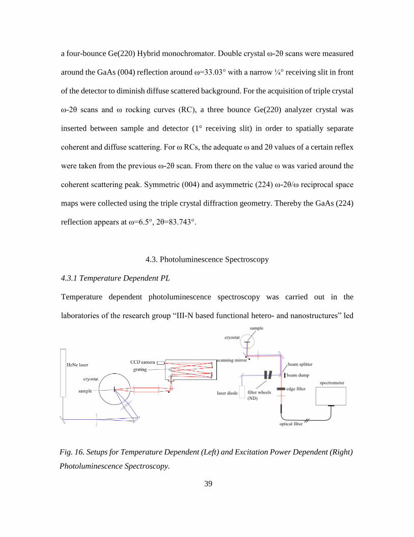
16. Setups for Temperature Dependent (Left) and Excitation Power Dependent (Right)
Photoluminescence Spectroscopy. ........................................................... 39
17. Spectrum of Bare Sample Holder at Maximal Laser Diode Power. The Spectrum
Contains a Broad Range of Spontaneous Radiation Emitted by the Laser
Diode and a Second Order Diffraction Replica of the Laser Line

xi
Figure Page
at 750 nm (Cut by Edge Filter). Most Importantly, the Wavelength Range
850-1050 nm Exhibits a Signal below the Noise Level............................ 41
18. DC ω-2θ Scans Collected in the Vicinity of the (004) GaAs Reflection for All
Samples, 475°C ≤ Tdep ≤ 520°C. .............................................................. 43
19. DC ω-2θ Scan of the Structure Grown at Tdep=505°C along with a Simulation Used
to Obtain Layer Thicknesses and Compound Compositions. .................. 44
20. TC ω RCs of All Samples 475°C ≤ Tdep ≤ 520°C. ............................................ 45
21. Symmetrical Reciprocal Space Maps for All Samples 475°C ≤ Tdep ≤ 520°C
Collected around the (004) 0 SL Spot of the MQW Structure. The 0SL Peak
of the MQW Structure Is Indicated by the Red Horizontal Bar, While the
-1SL Peak Is Located on the Black Horizontal Bar. ................................ 50
22. Asymmetrical Reciprocal Space Maps for All Samples 475°C ≤ Tdep ≤ 520°C
Collected around the (224) GaAs Diffraction. The (224) GaAs Diffraction
Spot Is Indicated by the Red Horizontal Bar, While the (224) SL Peak of the
MQW Structure Is Located on the Black Horizontal Bar. ....................... 51
23. Photoluminescence Spectrum of the Sample Tdep=505°C Measured at 5 K Ambient
Temperature. A Deconvolution of the Curve into Three Peaks Allows the
Individual Temperature Behavior to Be Studied. ..................................... 52
24. Temperature Evolution of the PL Transition Energies for the Three Peaks Indicated
in Fig. 23. The MQW Peak (Black Dots) Follows Neatly the Calculated
Transition Energy Obtained from Schrödinger-Poisson Simulations (Dashed
Line). ......................................................................................................... 53

xii
Figure Page
25. PL Spectra (12 K) with Increasing Excitation Power (from Black to Green Curve).
Spectra of Samples Tdep<505°C (A and B) Show Weak Sub-Bandgap
Luminescence, While Several Sub-Bandgap Transitions (Compare Fig. 23)
Appear for Tdep=505°C (C). Spectra Are Normalized and Stacked with
Increasing Excitation Power (0.07, 0.4, 1, 7.7 mW). ................................ 55
26. Integrated PL Intensity over Three Orders of Magnitude in Excitation Power
Measured at 12 K. Sample Tdep=505°C Reveals Brightest Luminescence. The
Gradation in Scaling Exponent among the Three Samples Indicates Distinct
Strengths of Non-Radiative SRH Recombination. .................................. 56
27. Whereas the Structures Tdep=505°C and Tdep=490°C Transition into the Linear
Regime, the Sample Tdep=475°C Reaches the Scaling Exponent 1.2. .... 57
28. The Shape of the EQE Curves Indicates That Auger Recombination Is Negligible
over the Covered Excitation Power Range, If Compared to Fig. 11 (Inset).
Even at Highest Pumping Level the MQW Emission Efficiency Does Not
Droop. ........................................................................................................ 58
29. A) Temperature Dependence of Central and Peak PL Transition Energy of the
Sample Tdep=520°C. B) Along with Linewidth and Integrated PL Intensity
Behavior, the Features Suggest the Presence of Random Band Edge
Fluctuations in the Sample. ....................................................................... 59
30. Illustration of How Carrier Localization in Local Energy Minima May Influence
Temperature Dependence of PL Transition Energy and Linewidth. [56] ...
.................................................................................................................... 60
xiii
Figure Page
31. Cross-Section TEM of the ×5-MQW Structure Grown at Tdep=520°C as Illustration
of Lateral Layer Thickness Modulations as a Result of Elevated Deposition
Temperature and Indium Decomposition. ................................................ 63
32. Multilayer Film Morphology of an Out-Of-Phase Instability. [59] ................... 64
xiv
LIST OF ACRONYMS
AES – Auger electron spectroscopy: Surface sensitive characterization technique for
element determination
AVP – automated valve positioner: steers a needle valve to regulate the emitted flux from
cracker cells as used for As in MBE setups
CF – confinement factor: ratio of modal gain to material gain in lasing structures
DL – dislocation loop: extended defect of both screw and edge type
FWHM – full width at half maximum: parameter expressing extent of peaked curves
HR-XRD – high resolution x-ray diffraction: non-destructive method for the analysis of
crystalline structures, such as semiconductor crystals, based on interference of x-ray
radiation, precise and highly sensitive setup allows to resolve fine structures (angles < 20
arc sec)
InGaAs – Indium-Gallium-Arsenide: Semiconducting ternary alloy of indium, gallium,
and arsenic; a representative of element III-element V compound semiconductors
MBE – molecular beam epitaxy: ultra-high vacuum technique for growth of semiconductor
crystals
MQW – multiple quantum well: the sequence of several SQWs
MSM – metal-semiconductor-metal: sandwich structure for metallic cavity nanolasers
ND – neutral density: refers to optical filters which exhibit constant attenuation over a wide
range of wavelengths
xv
OD – optical density: quantifies the degree of attenuation of optical filters in the reference
wavelength range, optical power before Pin and after Pout passing a filter OD is related by
Pout = Pin × 10−OD
PL – photoluminescence spectroscopy: optical technique in which light emitted from a
sample upon photo excitation is collected and interpreted spectrally resolved
RC – rocking curve: x-ray diffraction scan in which detector position 2θ is kept constant
and angle ω between source and sample is rocked around a diffraction value
RHEED – reflection high energy electron diffraction: a surface sensitive diffraction method
commonly used for in-situ surface morphology monitoring during MBE growth
RSM – reciprocal space map: x-ray diffraction multi-scan with correlated variation of
angles ω and 2θ, covering diffraction vectors of a specified area in reciprocal space
SPP – surface plasmon polariton: quasi-particle coupling photons confined to metal-
dielectric interface with charge oscillations
SQW – single quantum well: a low band gap material layer embedded between
comparatively higher band gap materials, acting as a confinement structure for carriers
SRH recombination – Shockley-Read-Hall recombination: non-radiative recombination
type mediated by defect states with energies within the semiconductor band gap
TEM – transmission electron microscopy: microscopy technique with way increased
resolution compared to conventional light microscope owing to the wave nature of
electrons
UHV – ultra high vacuum: vacuum conditions with residual pressure on the order of 10-10
mbar
1
CHAPTER 1
INTRODUCTION
“It is impossible to imaging now modern solid-state physics without semiconductor
heterostructures. Semiconductor heterostructures and, particularly, double
heterostructures, including quantum wells, wires, and dots, are today the subject of
research of two-thirds of the semiconductor physics community.” [2]
This introduction to 2000 Nobel Laureate Zhores Alferov’s Nobel lecture expresses the far
reaching impact invention and experimental realization of semiconductor heterostructures
have had on semiconductor science. This thesis is part of the strong research efforts on
heterostructures as it is dedicated to the growth and characterization of periodic
heterostructures composed of Indium-Gallium-Arsenide (InGaAs).
Early concepts of heterostructure devices used vertical changes in energy band gap to steer
the charge carrier movement through quasi-electric fields [3] or to concentrate carriers in
a particular volume of laser structures [4]. As soon as growth techniques became
sophisticated enough to deposit layer thicknesses at which quantum-size effects appeared
[5], the concept of heterostructuring enabled an unknown level of material and device
design. It allowed to tailor fundamental semiconductor crystal properties, such as effective
band gap energy, effective carrier masses, spatial carrier localization, and directional
carrier mobility as needed for a proposed device. With this tool at hand, a plethora of
heterostructure based devices has been developed, such as heterostructure light emitting
diodes, high electron mobility transistors, quantum well lasers, and heterostructure solar
cells resulting in omnipresent applications in modern communication, sensing, lighting,
energy generation, and many more. [2, 6]
2
Despite the great success of heterostructure devices there are still wide research areas to be
studied. The content of this thesis is such a one. Crystalline and physical properties of
semiconductor materials can vary a lot depending on the epitaxial growth conditions used
[7-10]. It is hence crucial for device design to consider correlations between physical
properties, crystal perfection of epitaxial structures, and growth conditions under which
desirable properties are achievable [11-14]. Suboptimal growth conditions may result in
structural deteriorations, which in turn are able to degrade device operation [15-19]. This
underlines the importance of the crystal structure as a determinant of device performance.
This study aims to establish correlations between molecular beam epitaxy (MBE) growth
conditions with crystalline and optical properties of InGaAs/GaAs multiple quantum well
(MQW) structures.
The thesis is structured as follows. After an introduction to metallic cavity nanolasers as
an application of InGaAs/GaAs MQW structures in Chapter 2, underlying concepts and
theories for this work are presented in Chapter 3. The reader is familiarized with epitaxial
growth by MBE and considerations on the creation of crystal defects. Two characterization
techniques, high resolution x-ray diffraction and photoluminescence spectroscopy, are
introduced and the examination of obtained data explained. A model relating light intensity
collected in an excitation power dependent photoluminescence experiment with non-
radiative trap state assisted recombination is proposed. Chapter 4 is dedicated to the
experimental procedures and setups used, while Chapter 5 focusses on the experimental
results obtained. Its outline resembles the interconnectedness of growth conditions,
crystalline, and physical properties stressed in this work. Conclusions are eventually drawn
in Chapter 6.
3
CHAPTER 2
APPLICATION OF INGAAS/GAAS MQWS
InGaAs/GaAs MQWs have a wide range of application, particularly in optoelectronic
devices including photovoltaics and semiconductor lasers. Two frontiers in their individual
research areas are MQW solar cells and nanolaser devices. The inclusion of MQWs into
solar cells promises higher photo-conversion efficiency as compared to a p-n-junction cell.
Enhanced optical absorption due to the two different bandgap energies involved increases
the short-circuit current, while carrier confinement in the nanostructures increases the
open-circuit voltage. [20-23]
In metallic cavity nanolasers, InGaAs/GaAs MQWs may serve as optically active region,
providing superior material gain. Sufficient optical gain is a major concern in this type of
lasing devices, as big losses due to adjacent metal layers must be compensated.
Nanolasers are coherent light sources with sizes comparable to or smaller than the
wavelength emitted (volume V < λ3). Wave guiding below the diffraction limit, however,
cannot be realized with conventional laser cavity designs. Metallic cavities represent a
promising approach to nanolasing devices. In such structures, the light field generated
within a semiconducting gain medium is confined by surrounding metal layers, due to the
strong interaction of photons with free electrons in the metal. The generation of such
surface plasmon polaritons (SPPs) is particularly strong near a specific photon energy (SPP
resonance), depending on the metal and geometry used. SPP coupling allows the effective
photon wavelength within the gain medium to be reduced substantially from its vacuum
value and hence enables optical confinement in small structures on the nanometer scale.
The quasi-particle generation does, however, involve considerable optical losses,
4
particularly around the SPP resonance, which need to be compensated by sufficient
material gain. In a trade-off approach, lasing modes need to be designed close to the
resonance energy to achieve strong confinement, but also far enough to obtain losses which
still can be overcome. It is beneficial that in metal-semiconductor-metal (MSM)
waveguides, a particular design approach, the SPP generation and resultant optical
confinement slows down the energy velocity of the light mode. This increases the gain per
unit length experienced by an amplified mode and translates into superior modal gain, as
compared to the usual situation of a plane wave in a uniform gain medium.1 The large
obtainable modal gain enables to overcome the optical losses.
MSM structures have the potential to reduce the size of semiconductor lasers below a few
tens of nanometers by providing strong optical confinement, with a confinement factor CF
> 1. Sufficient material gain in the semiconductor layers needs to overcome optical losses
resultant from the SPP generation.
Nanolasers may be the key to integrated photonics in all-optical communication and data
processing systems. Further, application in hybrid-integrated electronics to enable faster
on-chip communication may become feasible due to a reduction in size mismatch between
microelectronics and conventional optoelectronic devices. [24, 25]
First room temperature cw lasing under electrical injection has been demonstrated by Ding
et al. [26] in a structure depicted in Fig. 1. The InGaAs gain medium is covered with silver
to form the metallic cavity. The device (V = 0.42 λ3) has a threshold current of about 1000
1 modal gain = material gain × confinement factor, SPP generation allows CF>1
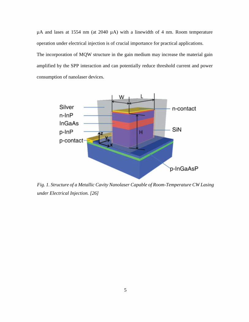
5
µA and lases at 1554 nm (at 2040 µA) with a linewidth of 4 nm. Room temperature
operation under electrical injection is of crucial importance for practical applications.
The incorporation of MQW structure in the gain medium may increase the material gain
amplified by the SPP interaction and can potentially reduce threshold current and power
consumption of nanolaser devices.
Fig. 1. Structure of a Metallic Cavity Nanolaser Capable of Room-Temperature CW Lasing
under Electrical Injection. [26]
6
CHAPTER 3
BASIC PRINCIPLES
3.1. Epitaxial Growth by Molecular Beam Epitaxy
3.1.1 Method of MBE Growth
Molecular beam epitaxy (MBE) is an ultra-high vacuum (UHV) technique, which is used
for the growth of monocrystalline semiconductor compounds. This growth technique
excels in the purity of the obtained compound crystals and the sharpness of grown material
interfaces. Both features are of special importance for the growth of device structures and
for the analysis presented in this thesis. Impurities can readily act as undesired dopants or
deep recombination levels and hence lead to unintended device performance, while sharp
material interfaces can serve as charge carrier confinement regions, which are the heart of
heterostructure devices. Abrupt material interfaces result from rather slow growth rates
(typically 0.1 – 2.0 µm/hour) that allow to interrupt material supply with 2 - 3 monolayers
precision and comparatively low growth temperatures leading to reduced interdiffusion at
the interface. [27]
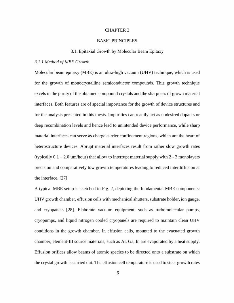
A typical MBE setup is sketched in Fig. 2, depicting the fundamental MBE components:
UHV growth chamber, effusion cells with mechanical shutters, substrate holder, ion gauge,
and cryopanels [28]. Elaborate vacuum equipment, such as turbomolecular pumps,
cryopumps, and liquid nitrogen cooled cryopanels are required to maintain clean UHV
conditions in the growth chamber. In effusion cells, mounted to the evacuated growth
chamber, element-III source materials, such as Al, Ga, In are evaporated by a heat supply.
Effusion orifices allow beams of atomic species to be directed onto a substrate on which
the crystal growth is carried out. The effusion cell temperature is used to steer growth rates
7
and compound concentrations (relative arrival rates of molecular beams), as it strongly
determines the emitted molecular fluxes. This is apparent from the solution of the
applicable Clausius-Clapeyron equation (assume ideal Knudsen cell). The emitted atomic
flux JMBE is proportional to the vapor pressure pv in the effusion cell
𝐽MBE ∝𝑝v
√𝑇∝
1
√𝑇exp(−
∆𝐻vap
𝑅𝑇)
with the cell temperature T, the universal gas constant R, and the evaporation enthalpy
ΔHvap of the particular source material. This exponential behavior of JMBE indeed represents
a sensitive dependence on the cell temperature T [29]. Element-V materials, such as As or
Sb are emitted from valved cracker cells, which provide small-molecular species, e.g. As2
to the growth chamber. Their fluxes are varied by a needle valve at the crucible outlet.
Mechanical shutters in front of each single effusion cell can interrupt beam fluxes within
Fig. 2. Sketch of the Basic Constituents of a Typical MBE Setup. Not Shown Are Buffer and
Intro Chamber Adjacent to the Growth Chamber, Which Serve as an Interlock System for
the Insertion and Removal of Samples. [28]
8
fractions of a second and hence allow the growth of complex layer designs. For calibration
purposes, the ion gauge (Beam Flux Monitor) can be exposed to the molecular beams in
order to determine the beam equivalent pressure (BEP), a measure of the incident
molecular flux, at various cell temperatures.
ln(𝑝BEP) = −∆𝐻vap
𝑅∙ 𝑇−1 + 𝐶,𝐶aparameter
Real MBE setups use Langmuir effusion cells, which operate at lower cell temperatures
and feature bigger effusion holes, as compared to the ideal Knudsen cell for which the
derivation is carried out. Slight deviations from the strict exponential dependence occur. In
growth mode, the material beams are directed onto the substrate, a monocrystal with high
crystalline quality, cut along a certain crystalline plane. Under favorable growth conditions
the impinging atoms can migrate on and stick to the growth surface and finally crystallize,
forming the desired crystal structure. The crystallization process sensitively depends on the
individual atomic fluxes, their ratio, the substrate temperature (deposition temperature
Tdep), atomic migration lengths, and the constitution of the substrate surface. These
parameters are among the growth conditions that can be varied in MBE.
The MBE technique will be utilized in the frame of this thesis to grow III-As
heterostructures with layer thicknesses as small as 8 nm.
3.1.2 Defect Creation in Epitaxial Growth
Epitaxial growth aims to transfer the crystal structure and a certain lattice orientation of a
substrate onto a deposited film. In case of III-As materials the underlying lattice structure
is of zincblende type, representative of the cubic crystal system.
9
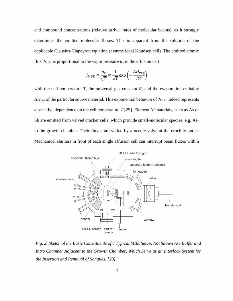
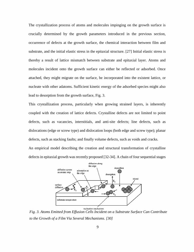
The crystallization process of atoms and molecules impinging on the growth surface is
crucially determined by the growth parameters introduced in the previous section,
occurrence of defects at the growth surface, the chemical interaction between film and
substrate, and the initial elastic stress in the epitaxial structure. [27] Initial elastic stress is
thereby a result of lattice mismatch between substrate and epitaxial layer. Atoms and
molecules incident onto the growth surface can either be reflected or adsorbed. Once
attached, they might migrate on the surface, be incorporated into the existent lattice, or
nucleate with other adatoms. Sufficient kinetic energy of the adsorbed species might also
lead to desorption from the growth surface, Fig. 3.
This crystallization process, particularly when growing strained layers, is inherently
coupled with the creation of lattice defects. Crystalline defects are not limited to point
defects, such as vacancies, interstitials, and anti-site defects; line defects, such as
dislocations (edge or screw type) and dislocation loops (both edge and screw type); planar
defects, such as stacking faults; and finally volume defects, such as voids and cracks.
An empirical model describing the creation and structural transformation of crystalline
defects in epitaxial growth was recently proposed [32-34]. A chain of four sequential stages
Fig. 3. Atoms Emitted from Effusion Cells Incident on a Substrate Surface Can Contribute
to the Growth of a Film Via Several Mechanisms. [30]
10
was identified, which may be realized successively to accommodate elastic strain, aiming
to stabilize the growth process. Each stage is characterized by specific preferred type of
crystalline defects, their density and spatial distribution in the volume, and a certain extent
of relaxation of initial elastic stress. The low deteriorate mode occurs in growth on high
crystal quality epitaxial layers, such as single crystal substrates. It involves the creation of
point defects, mixed type dislocation loops (60° dislocation loops in cubic structures), and
partial relaxation of the initial elastic stress to the physical limit ~70%.
At the initial stage, point defects are created at the growth front, considerably enhanced
under initial elastic stress. Inward diffusion of point defects into the epitaxial structures
leads to accumulation in pre-dislocation clusters. Their induced local secondary stress
finally triggers structural transformation of ripe clusters into primary dislocation loops
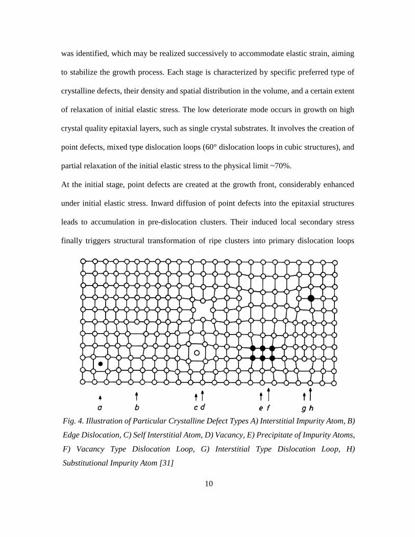
Fig. 4. Illustration of Particular Crystalline Defect Types A) Interstitial Impurity Atom, B)
Edge Dislocation, C) Self Interstitial Atom, D) Vacancy, E) Precipitate of Impurity Atoms,
F) Vacancy Type Dislocation Loop, G) Interstitial Type Dislocation Loop, H)
Substitutional Impurity Atom [31]
11
(DLs). At this stage, such dislocation loops penetrate deeply into the substrate and form
bottom closing edge segments there. Hence primary DLs do not contribute to relaxation of
initial elastic stress (pseudomorphic growth). Most primary DLs will not have top edge
segments, but follow the growth front and form wide trenches at the surface. Their
dislocation extra planes enhance point defect inward diffusion. At this stage primary DLs
(density 104 - 3∙106 cm-2) have reconstructed the growth front and rearranged spatial
distribution of elastic stress.
Continued growth leads to further point defect inward diffusion and accumulation in
clusters. A ripening process of pre-dislocation clusters results in the creation of 60°
secondary DLs (density 107 – 7∙1010 cm-2), which are smaller in spatial extent as compared
to their primary counterparts. Initially these loops will exhibit a closing edge segment in
the substrate and hence a significant fraction of secondary DLs does not contribute to
relaxation of initial elastic stress either. Further point defect accumulations, however, will
be concentrated around the epitaxial interface and lead to closing edge segment formation
close to it. This marks the onset of stress relaxation by secondary DL edge segments. The
extent of relaxation increases with the continued creation of edge segments close to the
epitaxial interface, until the physical limit of ~70% for 60° dislocations is reached.
Secondary dislocation loops are mainly realized as closed loops with top closing edge
segments. Continued defect creation will shift the location of top edge segments away from
the epitaxial interface into the epitaxial volume, which might be described as the formation
of tertiary DLs. All three kinds of DLs may intersect in the volume at high DL densities
resulting in the formation of Lomer dislocations.
12
Which stage might be finally realized does not only depend on growth parameters and
elastic properties of the epitaxial films, but its sequential realization is also determined by
the total thickness and multiplicity, in case of MQWs, of the epitaxial structure.
3.2. Assessing Crystalline Structure
It has been already pointed out that epitaxially grown semiconductor samples may exhibit
slight deviations from an ideally perfect crystalline structure with unperturbed periodicity.
Energy minimization and the thermodynamic trend of entropy maximization are
accountable for this occurrence of sub-perfect atomic arrangement. In order to analyze
structural properties on the scale of distances between crystal planes (GaAs: ~5.6 Å), the
utilization of a probe with dimensions on the same order of magnitude is required. X-ray
diffraction (XRD) (λ ~1.5 Å) has proven a reliable, non-destructive probe technique not
only for the analysis of semiconductor crystals. In the following sections, the features found
in XRD signals obtained from perfect crystals and specifically from semiconductor
heterostructures will be introduced. Deviations from these optimal features will be related
to extended defects created during epitaxial growth.
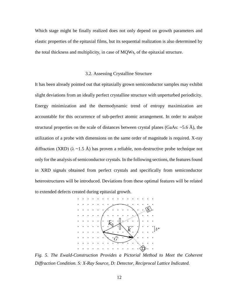
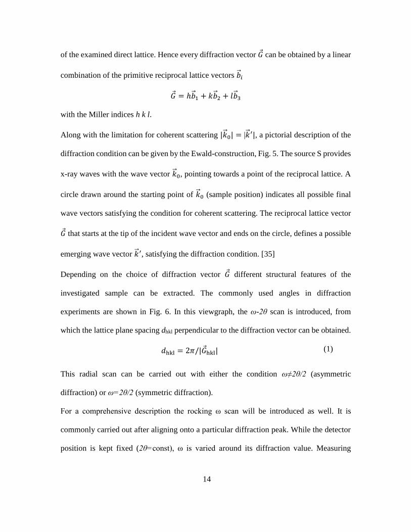
Fig. 5. The Ewald-Construction Provides a Pictorial Method to Meet the Coherent
Diffraction Condition. S: X-Ray Source, D: Detector, Reciprocal Lattice Indicated.
13
3.2.1 High Resolution X-Ray Diffraction on Semiconductor Heterostructures
In an x-ray diffraction experiment, coherent x-ray waves are incident onto the sample under
investigation. The angle of incidence can be varied continuously. The interaction of the x-
ray waves with the periodic crystal structure in the sample gives rise to the emergence of
x-ray radiation at several particular angles, depending on the specific type of crystal lattice.
The Laue equations summarize the necessary angular conditions to be met for constructive
interaction of x-rays with a crystalline structure. They can be expressed in the single term
�⃗� 0 − �⃗� ′ = 𝐺
with the incident and emerging wave vector �⃗� 0 and �⃗� ′, respectively, as well as a vector 𝐺
of the reciprocal lattice. The reciprocal lattice can be understood as the Fourier transform
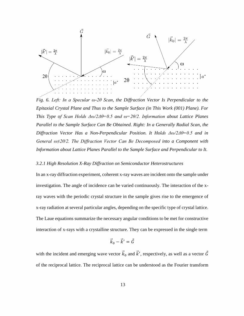
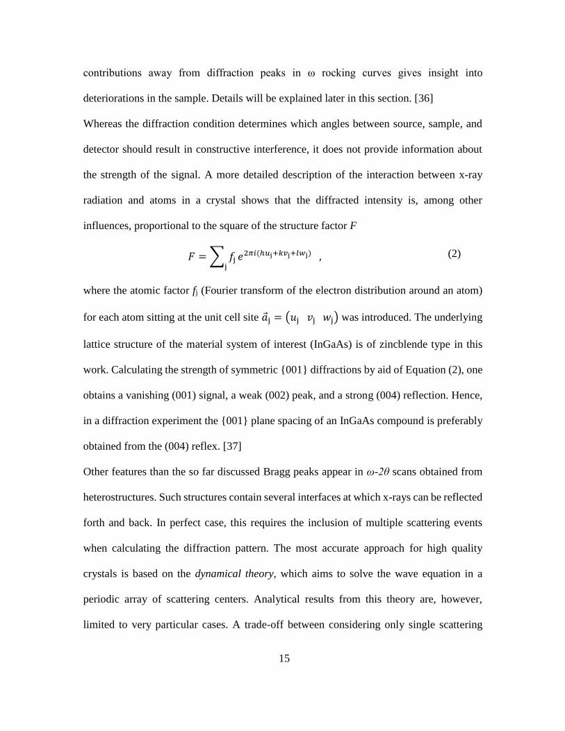
Fig. 6. Left: In a Specular ω-2θ Scan, the Diffraction Vector Is Perpendicular to the
Epitaxial Crystal Plane and Thus to the Sample Surface (in This Work (001) Plane). For
This Type of Scan Holds Δω/2Δθ=0.5 and ω=2θ/2. Information about Lattice Planes
Parallel to the Sample Surface Can Be Obtained. Right: In a Generally Radial Scan, the
Diffraction Vector Has a Non-Perpendicular Position. It Holds Δω/2Δθ=0.5 and in
General ω≠2θ/2. The Diffraction Vector Can Be Decomposed into a Component with
Information about Lattice Planes Parallel to the Sample Surface and Perpendicular to It.
14
of the examined direct lattice. Hence every diffraction vector 𝐺 can be obtained by a linear
combination of the primitive reciprocal lattice vectors �⃗� 𝑖
𝐺 = ℎ�⃗� 1 + 𝑘�⃗� 2 + 𝑙�⃗� 3
with the Miller indices h k l.
Along with the limitation for coherent scattering |�⃗� 0| = |�⃗� ′|, a pictorial description of the
diffraction condition can be given by the Ewald-construction, Fig. 5. The source S provides
x-ray waves with the wave vector �⃗� 0, pointing towards a point of the reciprocal lattice. A
circle drawn around the starting point of �⃗� 0 (sample position) indicates all possible final
wave vectors satisfying the condition for coherent scattering. The reciprocal lattice vector
𝐺 that starts at the tip of the incident wave vector and ends on the circle, defines a possible
emerging wave vector �⃗� ′, satisfying the diffraction condition. [35]
Depending on the choice of diffraction vector 𝐺 different structural features of the
investigated sample can be extracted. The commonly used angles in diffraction
experiments are shown in Fig. 6. In this viewgraph, the ω-2θ scan is introduced, from
which the lattice plane spacing dhkl perpendicular to the diffraction vector can be obtained.
𝑑hkl = 2𝜋/|𝐺 hkl| (1)
This radial scan can be carried out with either the condition ω≠2θ/2 (asymmetric
diffraction) or ω=2θ/2 (symmetric diffraction).
For a comprehensive description the rocking ω scan will be introduced as well. It is
commonly carried out after aligning onto a particular diffraction peak. While the detector
position is kept fixed (2θ=const), ω is varied around its diffraction value. Measuring
15
contributions away from diffraction peaks in ω rocking curves gives insight into
deteriorations in the sample. Details will be explained later in this section. [36]
Whereas the diffraction condition determines which angles between source, sample, and
detector should result in constructive interference, it does not provide information about
the strength of the signal. A more detailed description of the interaction between x-ray
radiation and atoms in a crystal shows that the diffracted intensity is, among other
influences, proportional to the square of the structure factor F
𝐹 = ∑ 𝑓j𝑒2𝜋𝑖(ℎ𝑢j+𝑘𝑣j+𝑙𝑤j)
j, (2)
where the atomic factor fj (Fourier transform of the electron distribution around an atom)
for each atom sitting at the unit cell site 𝑎 j = (𝑢j𝑣j𝑤j) was introduced. The underlying
lattice structure of the material system of interest (InGaAs) is of zincblende type in this
work. Calculating the strength of symmetric {001} diffractions by aid of Equation (2), one
obtains a vanishing (001) signal, a weak (002) peak, and a strong (004) reflection. Hence,
in a diffraction experiment the {001} plane spacing of an InGaAs compound is preferably
obtained from the (004) reflex. [37]
Other features than the so far discussed Bragg peaks appear in ω-2θ scans obtained from
heterostructures. Such structures contain several interfaces at which x-rays can be reflected
forth and back. In perfect case, this requires the inclusion of multiple scattering events
when calculating the diffraction pattern. The most accurate approach for high quality
crystals is based on the dynamical theory, which aims to solve the wave equation in a
periodic array of scattering centers. Analytical results from this theory are, however,
limited to very particular cases. A trade-off between considering only single scattering
16
events as done in the previous paragraphs (kinematical theory) and the full description by
the dynamical theory is given by the semikinematical approach. It can provide analytical
expressions for ω-2θ scans measured on MQW structures. In the following a MQW
structure, containing layer A and B grown pseudomorphically on material A is assumed.
Each layer has the thickness tA and tB, respectively. The pattern of A on B is sequenced N
times with the period p= tA+ tB. Treating this structure in the semikinematical framework
yields a diffraction intensity IMQW stemming from the MQW structure
𝐼MQW ∝(𝛷A𝛷B)𝑁 − 1
𝛷A𝛷B − 1 (3)
with the phase changes 𝛷Aand𝛷Bupon crossing a single layer A or B, respectively. From
this equation one can derive three prominent features:
1) The appearance of a zero order peak resultant from the MQW (0SL) at the angle
𝜔0SL = 𝜔A −2sin2(𝜔A)
sin(2𝜔A)∙
𝑡B𝑡A + 𝑡B
∙𝑎⏊,B − 𝑎A
𝑎A
(4)
with respect to the substrate Bragg peak at 𝜔A (see Equation (1)) and the vertical
lattice constants ai. Its position depends on the thickness of the individual layers,
the vertical lattice constant, and thus on the compound composition.
In fact, the 0SL peak appears at the angle where the Bragg peak of a single stressed
layer with the average compound composition of the MQW would be found.
2) Additionally, satellite peaks with the angular distance ∆𝜔SL to the zero order can
be found
∆𝜔SL = 𝑚sin(𝜔A)
sin(2𝜔A)∙𝜆
𝑝,𝑚 ∈ ℤ.
The angular distance depends on the period p of the MQW structure.
17
Features 1) and 2) appear at the angles satisfying (𝛷A𝛷B) = 1 in Equation (3).
3) Further, faster oscillations arise from the (𝛷A𝛷B)𝑁 term. The distance of these
interference fringes is given by
∆𝜔inter =sin(𝜔A)
sin(2𝜔A)∙
𝜆
𝑁𝑝
and is hence dependent on the total MQW thickness Np. Between two neighboring
satellite peaks, there will be N-2 interference fringes. [36, 38]
From the position and spacing of the satellite peaks one can determine individual layer
thicknesses and compound compositions. For the specific MQW design with N=5 , 𝑡A =
𝑡B =8 nm composed of In0.2Ga0.8As/GaAs grown pseudomorphically on a GaAs substrate
and probed with λ=1.5406 Å (Cu-Kα1) one obtains:
𝜔0SL − 𝜔GaAs = −0.52° = −31arcmin
∆𝜔SL = 0.33° = 20arcmin
∆𝜔inter = 0.066° = 3.9arcmin
3 interference fringes between adjacent satellite peaks
Knowing these three angular distances one can identify individual layer thicknesses,
material compositions, and the periodicity of the MQW structure.
18
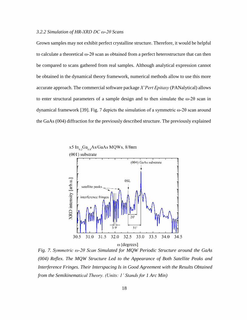
3.2.2 Simulation of HR-XRD DC ω-2θ Scans
Grown samples may not exhibit perfect crystalline structure. Therefore, it would be helpful
to calculate a theoretical ω-2θ scan as obtained from a perfect heterostructure that can then
be compared to scans gathered from real samples. Although analytical expression cannot
be obtained in the dynamical theory framework, numerical methods allow to use this more
accurate approach. The commercial software package X’Pert Epitaxy (PANalytical) allows
to enter structural parameters of a sample design and to then simulate the ω-2θ scan in
dynamical framework [39]. Fig. 7 depicts the simulation of a symmetric ω-2θ scan around
the GaAs (004) diffraction for the previously described structure. The previously explained
Fig. 7. Symmetric ω-2θ Scan Simulated for MQW Periodic Structure around the GaAs
(004) Reflex. The MQW Structure Led to the Appearance of Both Satellite Peaks and
Interference Fringes. Their Interspacing Is in Good Agreement with the Results Obtained
from the Semikinematical Theory. (Units: 1’ Stands for 1 Arc Min)
19
satellite peaks and interference fringes can be identified in the ω-2θ scan and their angular
distance compared to the analytical results given in the last section.
On the other hand, layer thicknesses, periodicities, and concentrations of real structures can
be obtained by reproducing their experimental HR-XRD curves.
3.2.3 Influence of Defects on HR-XRD Curves
Deviations from ω-2θ scans as simulated are mainly due to crystalline imperfections. The
use of a sufficiently involved experimental setup, e.g. with respect to instrumental x-ray
linewidth, is implied. Extended crystalline defects represent strong scattering centers at
which the coherence of the scattered x-ray field may be destroyed. The resultant diffraction
pattern will have contributions off the Bragg angles upon x-ray scattering at such
imperfections. This leads to a broadening of diffraction peaks and to the appearance of
diffuse scattering patterns. A loss in coherence diffuses interference fringes in ω-2θ scans
resultant from a MQW structure, as these fine features critically depend on coherent
interference throughout the entire structure and proper reflection at each interface.
Beside such qualitative comparisons, a quantitative evaluation can be done by calculating
the vertical coherence length Lvert.coh.. In case of the vertical coherence of a MQW region,
it is obtained from the linewidth Δω of a MQW peak in a symmetrical ω-2θ scan around
the Bragg peak ωB.
𝐿vert.coh. =0.9𝜆
2 cos(𝜔𝐵)∙ (∆𝜔)−1 ≈
8.263 ∙ 10−2
∆𝜔 [rad]⁄nm (5)
The approximate expression holds for (004) diffraction. In case of zincblende structures,
the vertical coherence is particularly diminished by closing edge segments in the volume
20
of an epitaxial structure, which can result from the intersection of two 60° dislocations.
[32, 33]
Information about the density, type, and distribution of extended defects created in a
sample can be gathered from ω-rocking curves (RC). A linewidth ΔωRC of the coherent
scattering peak obtained when rocking the angle ω can be interpreted as a density of
dislocations Ndisl. In case of 60° dislocation loops prominent in zincblende crystals an
estimate is given by
𝑁disl =∆𝜔RC
2
2𝜋ln(2)𝑏2 (6)
where ΔωRC is given in radians and b stands for the burgers vector [40]. The shape of the
diffuse scattering pattern away from the coherent peak gives insight into the type and
spatial lateral distribution of extended defects in the volume [41].
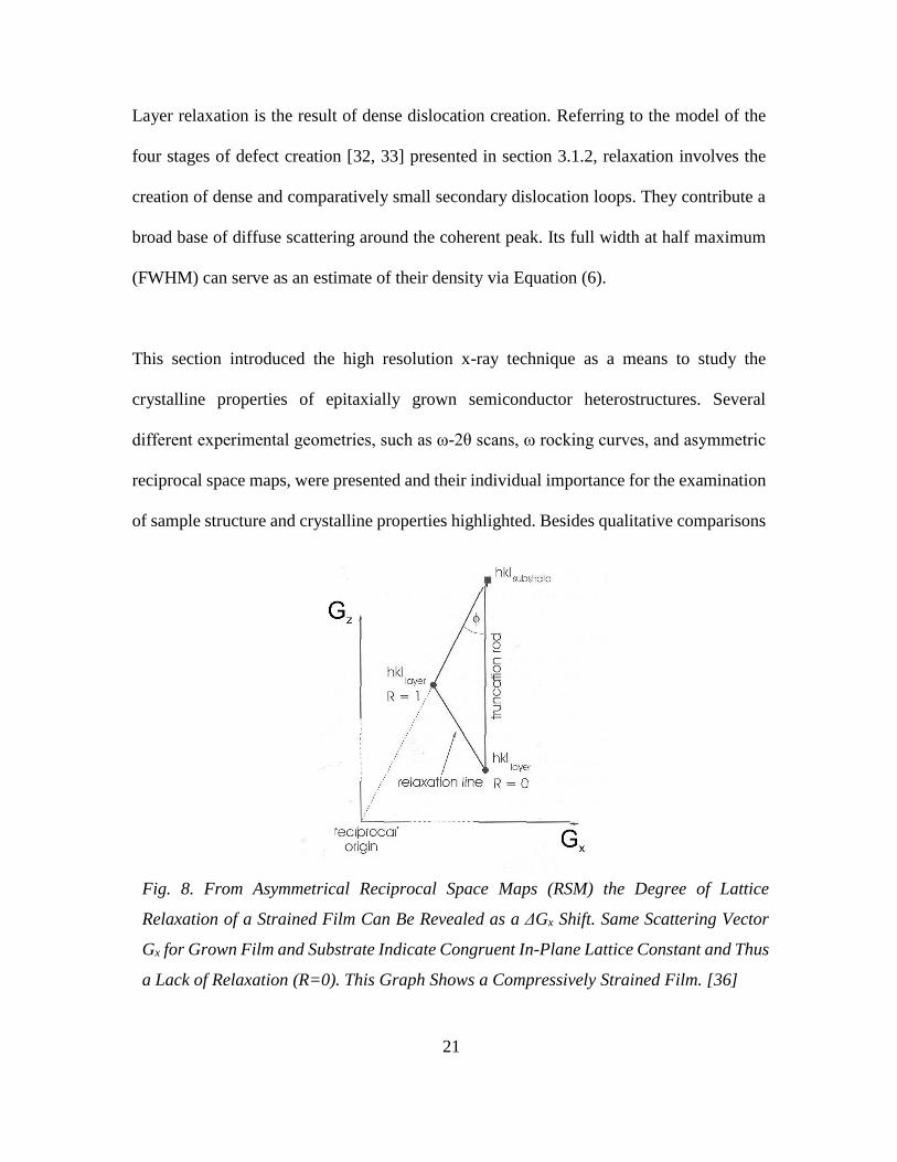
A combination of ω-2θ scans and ω RCs can be displayed in reciprocal space maps (RSM).
Whereas a symmetrical ω-2θ scan is running along Gz in reciprocal space, ω-2θ/ω RSMs
cover an area of scattering vectors with components Gz and Gx. They provide a pictorial
representation of the entire diffuse scattering stemming from crystal deteriorations and thus
can be utilized as a qualitative means to assess crystal quality. Whereas RSMs from perfect
structures are composed of pointlike coherent scattering connected by a narrow surface
truncation rod running along the Gz direction, crystal imperfections diminish pronunciation
of this interconnection and contribute extended areas of diffuse scattering. Asymmetrical
RSMs unveil the vertical and lateral lattice mismatch in heteroepitaxial structures. The
lateral lattice mismatch reflects the degree of relaxation R of individual layers (Fig. 8),
which can span the range from pseudomorphic (R=0) to almost entirely relaxed (R=1).
21
Layer relaxation is the result of dense dislocation creation. Referring to the model of the
four stages of defect creation [32, 33] presented in section 3.1.2, relaxation involves the
creation of dense and comparatively small secondary dislocation loops. They contribute a
broad base of diffuse scattering around the coherent peak. Its full width at half maximum
(FWHM) can serve as an estimate of their density via Equation (6).
This section introduced the high resolution x-ray technique as a means to study the
crystalline properties of epitaxially grown semiconductor heterostructures. Several
different experimental geometries, such as ω-2θ scans, ω rocking curves, and asymmetric
reciprocal space maps, were presented and their individual importance for the examination
of sample structure and crystalline properties highlighted. Besides qualitative comparisons
Fig. 8. From Asymmetrical Reciprocal Space Maps (RSM) the Degree of Lattice
Relaxation of a Strained Film Can Be Revealed as a ΔGx Shift. Same Scattering Vector
Gx for Grown Film and Substrate Indicate Congruent In-Plane Lattice Constant and Thus
a Lack of Relaxation (R=0). This Graph Shows a Compressively Strained Film. [36]
22
between a scattering response as expected from perfect structures and actually measured
curves, quantitative conclusions can be drawn from the motivated equations.
3.3. Examination of Optical Properties
While the technique presented in the previous section is capable of analyzing density and
distribution of extended defects created during epitaxial growth, it cannot definitely predict
their impact on physical properties. In order to gain an understanding of how as grown
structures might behave if applied in actual devices, the photoluminescence spectroscopy
(PL) technique will be utilized. Spectra obtained by PL give insight into strength of optical
loss paths, possible optical transitions, such as band edge emission or transitions between
charge carrier confinement states, and their individual strength. These information, in turn,
can be related to the structural features and specifically crystal deteriorations in the
examined samples.
In a crystal lattice, the periodic arrangement of atoms leads to specific bands of energy
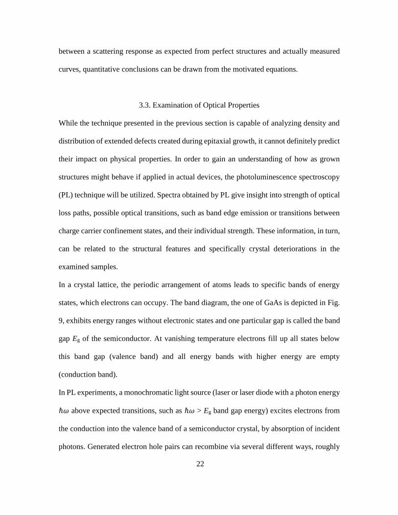
states, which electrons can occupy. The band diagram, the one of GaAs is depicted in Fig.
9, exhibits energy ranges without electronic states and one particular gap is called the band
gap Eg of the semiconductor. At vanishing temperature electrons fill up all states below
this band gap (valence band) and all energy bands with higher energy are empty
(conduction band).
In PL experiments, a monochromatic light source (laser or laser diode with a photon energy
ℏ𝜔 above expected transitions, such as ℏ𝜔 > Eg band gap energy) excites electrons from
the conduction into the valence band of a semiconductor crystal, by absorption of incident
photons. Generated electron hole pairs can recombine via several different ways, roughly
23
categorized into radiative and non-radiative recombination, depending on if a photon is
released or not. The emitted light is collected, spectrally resolved, and the obtained spectra
analyzed with respect to position and intensity of identified peaks. More details on the used
experimental setups will be presented in section 4.3.
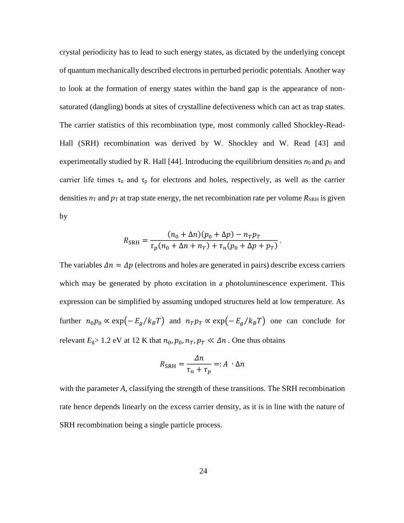
3.3.1 Shockley-Read-Hall Recombination
One of the non-radiative types of electron hole pair recombination is mediated by energy
states that lie within the band gap of a semiconductor crystal. Single carriers recombine
with a trap site of a specific charge state. The released energy is transferred to multiple
phonons generated. Strict lattice periodicity prohibits the existence of energy states in this
energy range. Their appearance can be related to disruptions of a perfect lattice, e.g. by
point defects, such as vacancies and interstitials, or dislocations. Any deviation from a
Fig. 9. Band Structure of the GaAs Crystal at Energies around the Band Gap at 300 K.
Different States of Spin-Orbit Coupling Lift the Degeneracy of the Valence Band. At the Γ
Point (Vanishing Wave Vector), However, Light Hole and Heavy Hole Bands Are
Degenerate. [42]
24
crystal periodicity has to lead to such energy states, as dictated by the underlying concept
of quantum mechanically described electrons in perturbed periodic potentials. Another way
to look at the formation of energy states within the band gap is the appearance of non-
saturated (dangling) bonds at sites of crystalline defectiveness which can act as trap states.
The carrier statistics of this recombination type, most commonly called Shockley-Read-
Hall (SRH) recombination was derived by W. Shockley and W. Read [43] and
experimentally studied by R. Hall [44]. Introducing the equilibrium densities n0 and p0 and
carrier life times τn and τp for electrons and holes, respectively, as well as the carrier
densities nT and pT at trap state energy, the net recombination rate per volume RSRH is given
by
𝑅SRH =(𝑛0 + Δ𝑛)(𝑝0 + Δ𝑝) − 𝑛𝑇𝑝𝑇
𝜏𝑝(𝑛0 + Δ𝑛 + 𝑛𝑇) + 𝜏𝑛(𝑝0 + Δ𝑝 + 𝑝𝑇).
The variables 𝛥𝑛 = 𝛥𝑝 (electrons and holes are generated in pairs) describe excess carriers
which may be generated by photo excitation in a photoluminescence experiment. This
expression can be simplified by assuming undoped structures held at low temperature. As
further 𝑛0𝑝0 ∝ exp(−𝐸𝑔 𝑘𝐵𝑇⁄ ) and 𝑛𝑇𝑝𝑇 ∝ exp(−𝐸𝑔 𝑘𝐵𝑇⁄ ) one can conclude for
relevant Eg> 1.2 eV at 12 K that 𝑛0, 𝑝0, 𝑛𝑇 , 𝑝𝑇 ≪ 𝛥𝑛. One thus obtains
𝑅SRH =𝛥𝑛
𝜏𝑛 + 𝜏𝑝=:𝐴 ∙ Δ𝑛
with the parameter A, classifying the strength of these transitions. The SRH recombination
rate hence depends linearly on the excess carrier density, as it is in line with the nature of
SRH recombination being a single particle process.
25
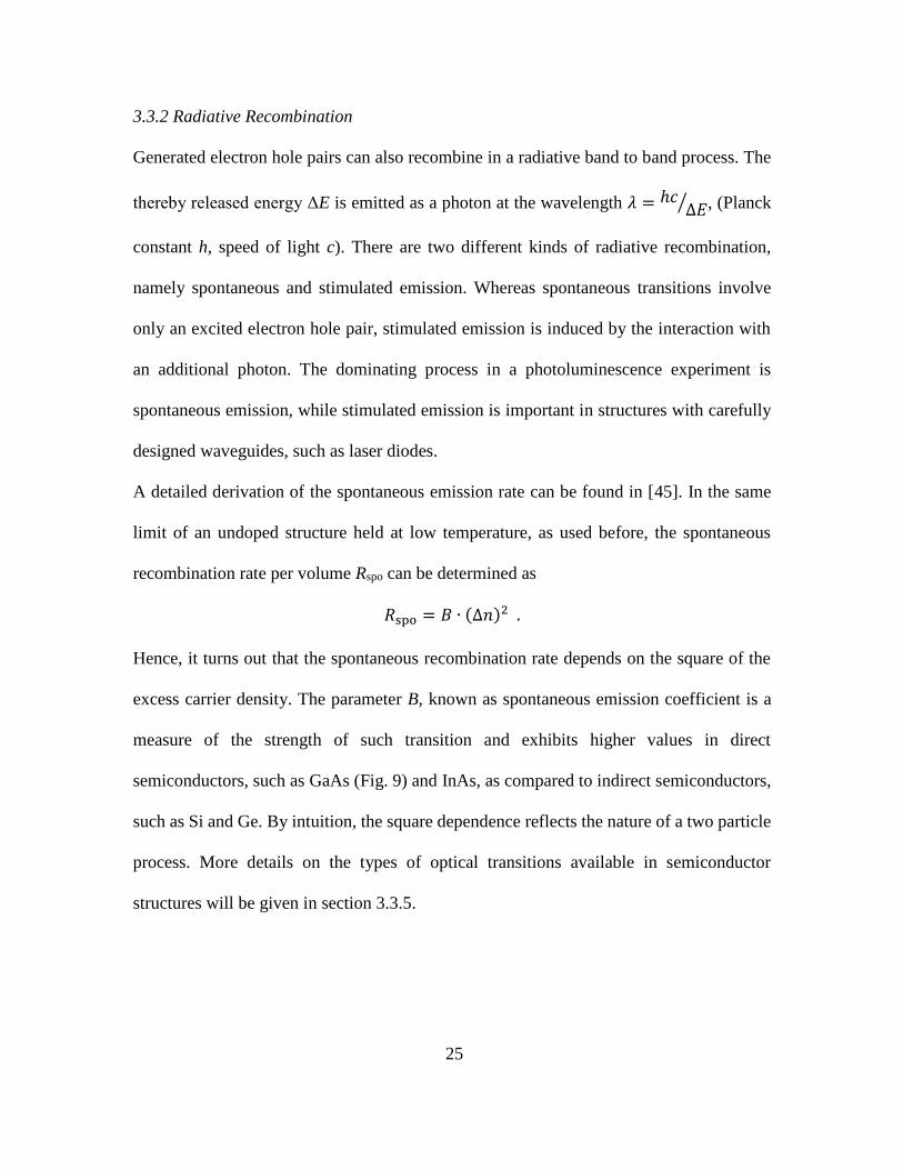
3.3.2 Radiative Recombination
Generated electron hole pairs can also recombine in a radiative band to band process. The
thereby released energy ΔE is emitted as a photon at the wavelength 𝜆 = ℎ𝑐∆𝐸⁄ , (Planck
constant h, speed of light c). There are two different kinds of radiative recombination,
namely spontaneous and stimulated emission. Whereas spontaneous transitions involve
only an excited electron hole pair, stimulated emission is induced by the interaction with
an additional photon. The dominating process in a photoluminescence experiment is
spontaneous emission, while stimulated emission is important in structures with carefully
designed waveguides, such as laser diodes.
A detailed derivation of the spontaneous emission rate can be found in [45]. In the same
limit of an undoped structure held at low temperature, as used before, the spontaneous
recombination rate per volume Rspo can be determined as
𝑅spo = 𝐵 ∙ (∆𝑛)2.
Hence, it turns out that the spontaneous recombination rate depends on the square of the
excess carrier density. The parameter B, known as spontaneous emission coefficient is a
measure of the strength of such transition and exhibits higher values in direct
semiconductors, such as GaAs (Fig. 9) and InAs, as compared to indirect semiconductors,
such as Si and Ge. By intuition, the square dependence reflects the nature of a two particle
process. More details on the types of optical transitions available in semiconductor
structures will be given in section 3.3.5.

26
3.3.3 Auger Recombination
The Auger-effect generally describes a non-radiative energy transfer between two electrons
in an atomic shell. When an atom is excited, for instance by x-rays, lifting a shell electron,
this electron can relax to its ground state and thereby transfer its energy to another shell-
electron which thereupon leaves the atom as a so-called Auger-electron. This phenomenon
was first observed and described by L. Meitner [46] and is nowadays applied as a
spectroscopic technique (AES), which allows to determine chemical compositions of
materials.
In semiconductor-respect the basic effect can be observed, too. The reading, however,
deviates a little bit: Auger events involve nnp- (a hole and an electron recombine by
transferring their energy to an additional electron) and npp-processes (excited hole) -
transitions occur between bands. Further, the excited ("hot") carrier thermalizes by the
emission of phonons.
This three particle process occurs at the rate
𝑅Auger = 𝐶 ∙ (∆𝑛)3
with the Auger coefficient C [45].
27
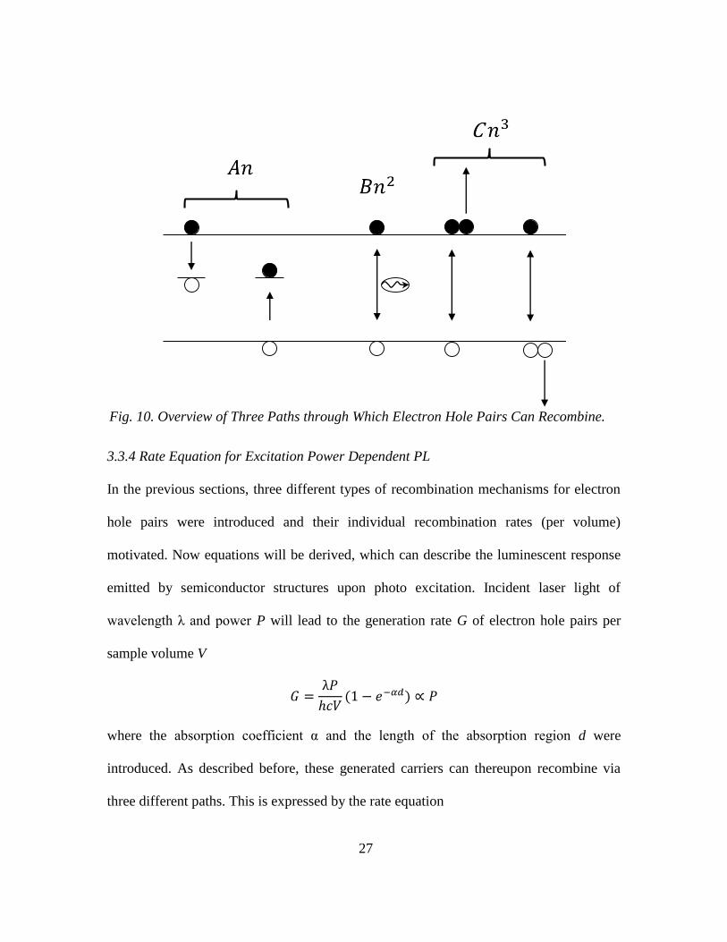
3.3.4 Rate Equation for Excitation Power Dependent PL
In the previous sections, three different types of recombination mechanisms for electron
hole pairs were introduced and their individual recombination rates (per volume)
motivated. Now equations will be derived, which can describe the luminescent response
emitted by semiconductor structures upon photo excitation. Incident laser light of
wavelength λ and power P will lead to the generation rate G of electron hole pairs per
sample volume V
𝐺 =λ𝑃
ℎ𝑐𝑉(1 − 𝑒−𝛼𝑑) ∝ 𝑃
where the absorption coefficient α and the length of the absorption region d were
introduced. As described before, these generated carriers can thereupon recombine via
three different paths. This is expressed by the rate equation
Fig. 10. Overview of Three Paths through Which Electron Hole Pairs Can Recombine.
28
d𝑛
d𝑡= 𝐺 − 𝐴𝑛 − 𝐵𝑛2 − 𝐶𝑛3,
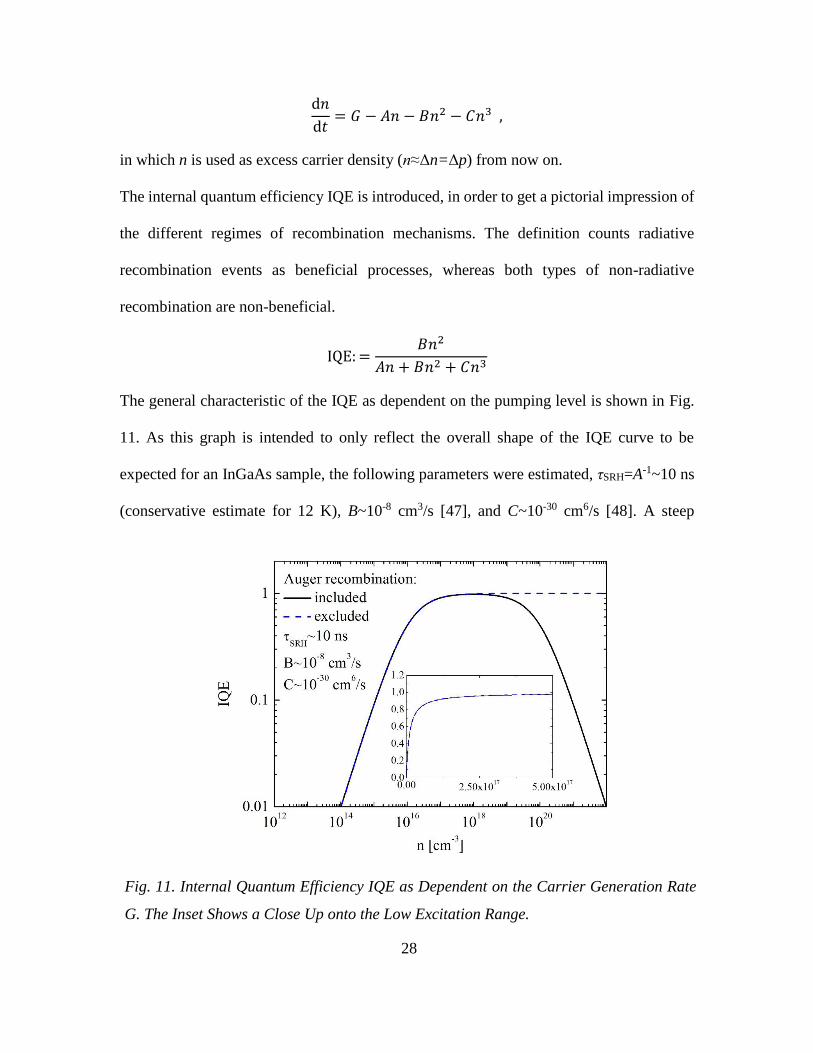
in which n is used as excess carrier density (n≈Δn=Δp) from now on.
The internal quantum efficiency IQE is introduced, in order to get a pictorial impression of
the different regimes of recombination mechanisms. The definition counts radiative
recombination events as beneficial processes, whereas both types of non-radiative
recombination are non-beneficial.
IQE:=𝐵𝑛2
𝐴𝑛 + 𝐵𝑛2 + 𝐶𝑛3
The general characteristic of the IQE as dependent on the pumping level is shown in Fig.
11. As this graph is intended to only reflect the overall shape of the IQE curve to be
expected for an InGaAs sample, the following parameters were estimated, τSRH=A-1~10 ns
(conservative estimate for 12 K), B~10-8 cm3/s [47], and C~10-30 cm6/s [48]. A steep
Fig. 11. Internal Quantum Efficiency IQE as Dependent on the Carrier Generation Rate
G. The Inset Shows a Close Up onto the Low Excitation Range.
29
increase in IQE at low carrier densities n is followed by a plateau with maximal IQE. In
this regime SRH-recombination becomes less and less important and the radiative
recombination dominates finally. Further increase in excitation power leads to an IQE
decrease, as the non-radiative Auger recombination type becomes stronger. The plot also
contains the IQE curve for the case of vanishing Auger recombination, which coincides
with the curve based on the full equation until the onset of the IQE decrease. It can be
concluded that at low and intermediate generation rates G, one can enter a recombination
regime, which can be described by SRH- and radiative recombination only. Making use of
this limit of low excitation, the rate equation at steady state simplifies to
0 = 𝑛2 +𝐴
𝐵𝑛 −
𝐺
𝐵,
which can be solved for the excess carrier density
𝑛 = −𝐴
2𝐵+ √(
𝐴
2𝐵)2
+𝐺
𝐵.
Under these conditions the rate of photons �̇� emitted from a sample with the optical volume
V is given by
�̇�(𝐺) = 𝑉𝐵𝑛2 = 𝑉𝐵 [−𝐴
2𝐵+ √(
𝐴
2𝐵)2
+𝐺
𝐵]
2
(7)
A sample plot of this equation in depicted in Fig. 12 (black, solid). The obtained curve may
represent the light intensity emitted from a sample in an excitation power dependent PL
experiment. Two different regimes can be identified, depending on the excitation power.
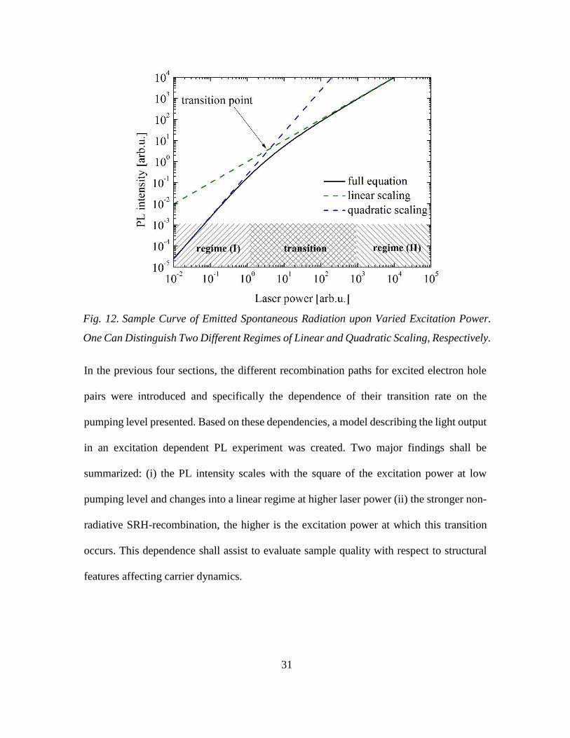
Regime (I): At low pumping level, only a small portion of the electron hole pairs
recombines radiatively, but rather saturates trap states in the sample. The PL intensity
30
scales with the square of the excitation power. Equation (7) can be approximated in the
limit 𝐵𝐺 𝐴2 ≪ 1⁄ as
�̇� = 𝑉𝐵
𝐴2𝐺2 ∝ 𝐺2.
Regime (II): At high enough excitation, trap states are mainly saturated and recombination
occurs predominantly radiatively. The emitted PL intensity depends linearly on the
excitation level. In this limit of 𝑛 ≈ √𝐺 𝐵⁄ , Equation (7) can be approximated as
�̇� = 𝑉𝐺 ∝ 𝐺
The transition between these two distinct regimes occurs continuously�̇� ∝ 𝐺𝑘, with a
gradual decrease of the scaling parameter𝑘 ∈ (1,2). A particular value of the power at
which the transition occurs can be defined as the excitation level GT at which the curves,
approximated in the individual limits, intersect 𝑉𝐵𝐺T2 𝐴2 = 𝑉𝐺T⁄ . Since the generation
rate at this point is given by
𝐺T =𝐴2
𝐵∝ 𝐴2
the pumping level at which the transition from regime (I) to (II) occurs can be used as a
measure of the magnitude of the A parameter and hence of the strength of trap states in the
investigated sample.
31
In the previous four sections, the different recombination paths for excited electron hole
pairs were introduced and specifically the dependence of their transition rate on the
pumping level presented. Based on these dependencies, a model describing the light output
in an excitation dependent PL experiment was created. Two major findings shall be
summarized: (i) the PL intensity scales with the square of the excitation power at low
pumping level and changes into a linear regime at higher laser power (ii) the stronger non-
radiative SRH-recombination, the higher is the excitation power at which this transition
occurs. This dependence shall assist to evaluate sample quality with respect to structural
features affecting carrier dynamics.
Fig. 12. Sample Curve of Emitted Spontaneous Radiation upon Varied Excitation Power.
One Can Distinguish Two Different Regimes of Linear and Quadratic Scaling, Respectively.
32
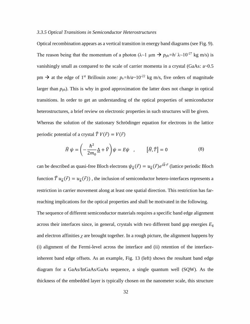
3.3.5 Optical Transitions in Semiconductor Heterostructures
Optical recombination appears as a vertical transition in energy band diagrams (see Fig. 9).
The reason being that the momentum of a photon (λ~1 µm pph=h/ λ~10-27 kg m/s) is
vanishingly small as compared to the scale of carrier momenta in a crystal (GaAs: a~0.5
pm at the edge of 1st Brillouin zone: pe=h/a~10-22 kg m/s, five orders of magnitude
larger than pph). This is why in good approximation the latter does not change in optical
transitions. In order to get an understanding of the optical properties of semiconductor
heterostructures, a brief review on electronic properties in such structures will be given.
Whereas the solution of the stationary Schrödinger equation for electrons in the lattice
periodic potential of a crystal �̂�𝑉(𝑟 ) = 𝑉(𝑟 )
�̂�𝜓 = (−ℏ2
2𝑚0∆ + �̂�)𝜓 = 𝐸𝜓,[�̂�, �̂�] = 0 (8)
can be described as quasi-free Bloch electrons 𝜓�⃗� (𝑟 ) = 𝑢�⃗�
(𝑟 )𝑒𝑖�⃗� ∙𝑟 (lattice periodic Bloch
function 𝑇̂𝑢�⃗� (𝑟 ) = 𝑢�⃗�
(𝑟 )) , the inclusion of semiconductor hetero-interfaces represents a
restriction in carrier movement along at least one spatial direction. This restriction has far-
reaching implications for the optical properties and shall be motivated in the following.
The sequence of different semiconductor materials requires a specific band edge alignment
across their interfaces since, in general, crystals with two different band gap energies Eg
and electron affinities χ are brought together. In a rough picture, the alignment happens by
(i) alignment of the Fermi-level across the interface and (ii) retention of the interface-
inherent band edge offsets. As an example, Fig. 13 (left) shows the resultant band edge
diagram for a GaAs/InGaAs/GaAs sequence, a single quantum well (SQW). As the
thickness of the embedded layer is typically chosen on the nanometer scale, this structure
33
causes the confinement of carriers in this quantum well. As a consequence, electrons and
holes can no more be considered quasi-free, but occupy states quantized (quantum number
n) along the growth direction z. The resultant wave function contains a quasi-free
component along the interface (wave vector �⃗� ⏊) and an envelope function χn(z) as a result
of the confinement.
𝜓�⃗� (𝑛)(𝑟 ) = 𝑢�⃗�
(𝑟 )𝑒𝑖�⃗� ⏊∙𝑟 𝜒n(𝑧)
For low quantum numbers n, the envelope function χn(z) describes a standing wave within
the well and has a decaying component in the barrier material. In case of multiple quantum
wells (MQWs), the evanescent components of each well may interact with each other and
form an overall envelope function with, again, quantized energy values. In Fig. 13 (right),
the band edge diagram along growth direction is shown for a × 5-MQW structure with all
layers 8 nm thick and a sequence of In0.2Ga0.8As/GaAs. Further, the ground state (n=1) for
the conduction and the heavy- and light- hole valence band are included.
Considering the optical response of such structures, the confinement of carriers implies
transitions to occur between these discrete quantum states. Although there is a continuum
of energy states available with wave vectors perpendicular to the growth direction, the
relaxation process to the band edge occurs on a faster time scale than the photon emission
and hence these quantum state energies are crucial for optical spectra. As the strength Ri,f
of an optical transition between two states ψi and ψf is determined by the magnitude of the
matrix element of the perturbing light field Hamiltonian �̂�opt, 𝑅i,f ∝ |⟨𝜓𝑖|�̂�opt|𝜓𝑓⟩|2 [49],
one can deduce that such optical transitions are specifically strong in which the quantum
number n does not change (Δn=0), e.g. between the individual confinement ground states.
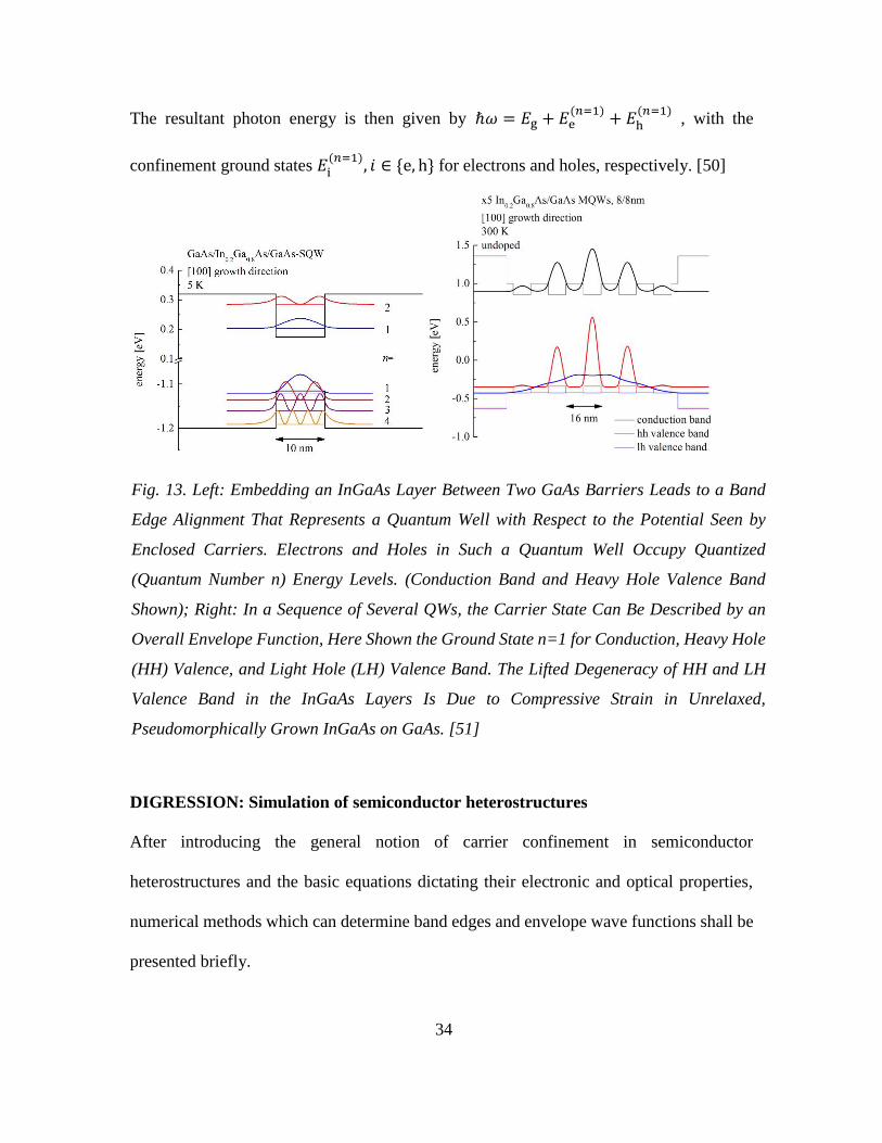
34
The resultant photon energy is then given by ℏ𝜔 = 𝐸g + 𝐸e(𝑛=1)
+ 𝐸h(𝑛=1)
, with the
confinement ground states 𝐸i(𝑛=1)
, 𝑖 ∈ {e, h} for electrons and holes, respectively. [50]
DIGRESSION: Simulation of semiconductor heterostructures
After introducing the general notion of carrier confinement in semiconductor
heterostructures and the basic equations dictating their electronic and optical properties,
numerical methods which can determine band edges and envelope wave functions shall be
presented briefly.
Fig. 13. Left: Embedding an InGaAs Layer Between Two GaAs Barriers Leads to a Band
Edge Alignment That Represents a Quantum Well with Respect to the Potential Seen by
Enclosed Carriers. Electrons and Holes in Such a Quantum Well Occupy Quantized
(Quantum Number n) Energy Levels. (Conduction Band and Heavy Hole Valence Band
Shown); Right: In a Sequence of Several QWs, the Carrier State Can Be Described by an
Overall Envelope Function, Here Shown the Ground State n=1 for Conduction, Heavy Hole
(HH) Valence, and Light Hole (LH) Valence Band. The Lifted Degeneracy of HH and LH
Valence Band in the InGaAs Layers Is Due to Compressive Strain in Unrelaxed,
Pseudomorphically Grown InGaAs on GaAs. [51]
35
It is a hopeless endeavor to solve Equation (8) for all wave vectors �⃗� without any
approximation. It is, however, feasible to get solutions with wave vectors around a
particular point in reciprocal space, especially in optoelectronic context commonly chosen
as the Γ point. Ground states for this particular value k=0 can indeed be approximated
numerically and small deviations from k=0 are treated in the framework of perturbation
theory with the perturbing Hamiltonian �̂�p =ℏ
𝑚0�⃗� ∙ 𝑝 ̂, where 𝑝 ̂ is the momentum operator.
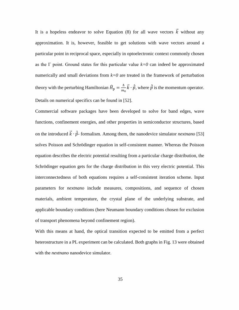
Details on numerical specifics can be found in [52].
Commercial software packages have been developed to solve for band edges, wave
functions, confinement energies, and other properties in semiconductor structures, based
on the introduced �⃗� ∙ 𝑝 ̂- formalism. Among them, the nanodevice simulator nextnano [53]
solves Poisson and Schrödinger equation in self-consistent manner. Whereas the Poisson
equation describes the electric potential resulting from a particular charge distribution, the
Schrödinger equation gets for the charge distribution in this very electric potential. This
interconnectedness of both equations requires a self-consistent iteration scheme. Input
parameters for nextnano include measures, compositions, and sequence of chosen
materials, ambient temperature, the crystal plane of the underlying substrate, and
applicable boundary conditions (here Neumann boundary conditions chosen for exclusion
of transport phenomena beyond confinement region).
With this means at hand, the optical transition expected to be emitted from a perfect
heterostructure in a PL experiment can be calculated. Both graphs in Fig. 13 were obtained
with the nextnano nanodevice simulator.
36
CHAPTER 4
EXPERIMENTAL PROCEDURES
After reviewing theoretical aspects fundamental to this work, the utilized setups and
experimental procedures will be introduced. So far it has been shown that HR-XRD and
PL are suitable techniques to characterize crystalline and optical properties. This work aims
to correlate them with chosen MBE growth conditions. MBE has been presented as a
powerful technique for the growth of heterostructures with precise interfaces.
4.1. Molecular Beam Epitaxy
Epitaxial growth was carried out in the Solar Power Laboratory2 with a VEECO GEN III
MBE system. The growth chamber was equipped with a RHEED (reflection high energy
electron diffraction) setup for in-situ monitoring of the surface morphology. Background
pressure before growth was on the order of 10-9 torr. Undoped (001) GaAs wafers with an
oxide capping were introduced to the growth chamber onto the substrate holder. Successive
increase of sample holder temperature was monitored with RHEED and a pyrometer until
deoxidation of the wafer occurred. Deoxidation is indicated by a change from a
diffuse/spotty to a bright streaky RHEED pattern, as the surface morphology changes from
an amorphous to a crystalline texture. The pyrometer was calibrated to the occurrence of
deoxidation at Tdeox=580°C. To complete the deoxidation process the sample was kept at
610°C for 15 min under As-overpressure. The entire growth process was carried out under
As-rich conditions (As-cell cracker/bulk temperature was 960/405°C), so the growth rate
2 Solar Power Laboratory, Arizona State University Research Park, 7700 S. River
Parkway, Tempe, AZ 85284, USA
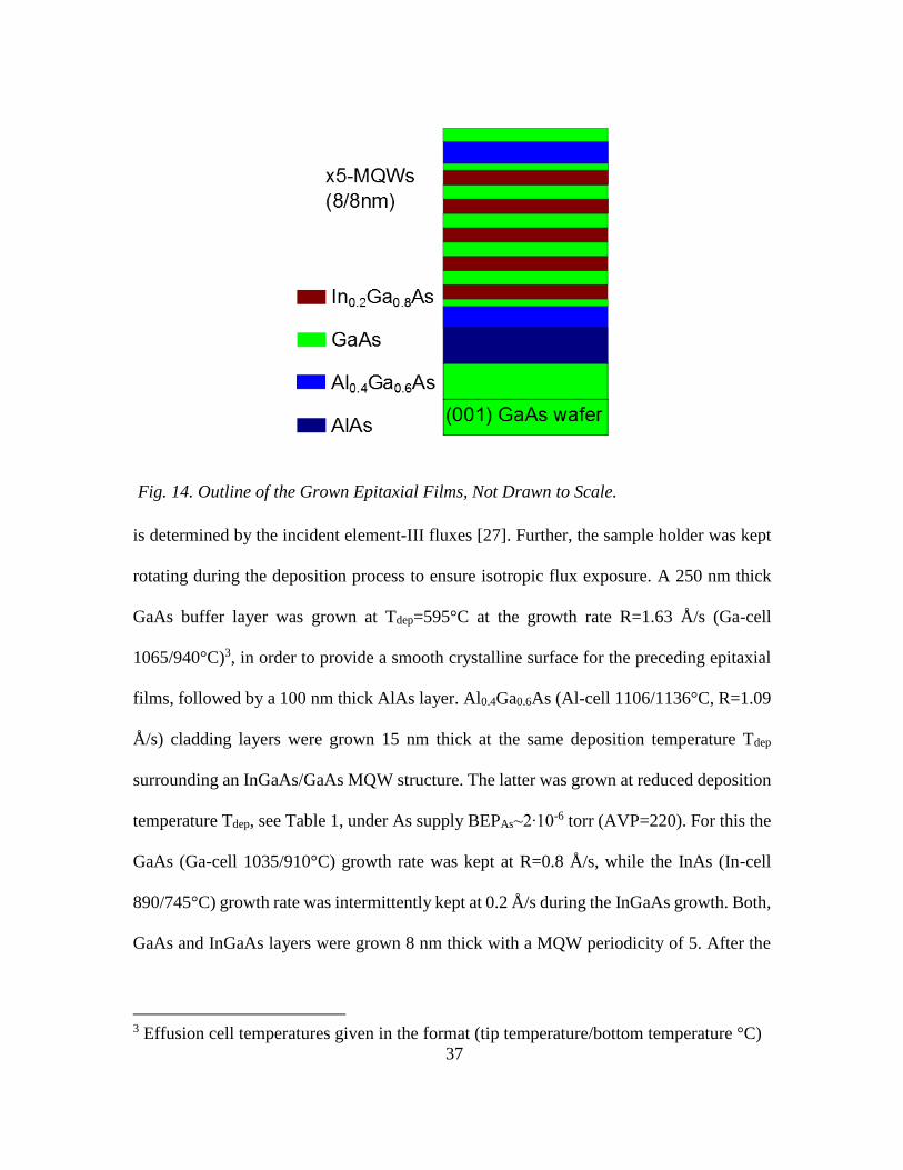
37
is determined by the incident element-III fluxes [27]. Further, the sample holder was kept
rotating during the deposition process to ensure isotropic flux exposure. A 250 nm thick
GaAs buffer layer was grown at Tdep=595°C at the growth rate R=1.63 Å/s (Ga-cell
1065/940°C)3, in order to provide a smooth crystalline surface for the preceding epitaxial
films, followed by a 100 nm thick AlAs layer. Al0.4Ga0.6As (Al-cell 1106/1136°C, R=1.09
Å/s) cladding layers were grown 15 nm thick at the same deposition temperature Tdep
surrounding an InGaAs/GaAs MQW structure. The latter was grown at reduced deposition
temperature Tdep, see Table 1, under As supply BEPAs~2∙10-6 torr (AVP=220). For this the
GaAs (Ga-cell 1035/910°C) growth rate was kept at R=0.8 Å/s, while the InAs (In-cell
890/745°C) growth rate was intermittently kept at 0.2 Å/s during the InGaAs growth. Both,
GaAs and InGaAs layers were grown 8 nm thick with a MQW periodicity of 5. After the
3 Effusion cell temperatures given in the format (tip temperature/bottom temperature °C)
Fig. 14. Outline of the Grown Epitaxial Films, Not Drawn to Scale.
38
growth, the sample cooled down under As exposure and was then removed from the growth
chamber. The entire structure is depicted in Fig. 14. In0.2Ga0.8As is lattice mismatched by
1.4% to GaAs.
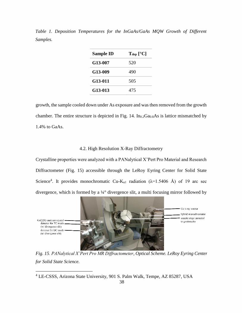
4.2. High Resolution X-Ray Diffractometry
Crystalline properties were analyzed with a PANalytical X’Pert Pro Material and Research
Diffractometer (Fig. 15) accessible through the LeRoy Eyring Center for Solid State
Science4. It provides monochromatic Cu-Kα1 radiation (λ=1.5406 Å) of 19 arc sec
divergence, which is formed by a ¼° divergence slit, a multi focusing mirror followed by
4 LE-CSSS, Arizona State University, 901 S. Palm Walk, Tempe, AZ 85287, USA
Table 1. Deposition Temperatures for the InGaAs/GaAs MQW Growth of Different
Samples.
Sample ID Tdep [°C]
G13-007 520
G13-009 490
G13-011 505
G13-013 475
Fig. 15. PANalytical X’Pert Pro MR Diffractometer, Optical Scheme. LeRoy Eyring Center
for Solid State Science.
39
a four-bounce Ge(220) Hybrid monochromator. Double crystal ω-2θ scans were measured
around the GaAs (004) reflection around ω=33.03° with a narrow ¼° receiving slit in front
of the detector to diminish diffuse scattered background. For the acquisition of triple crystal
ω-2θ scans and ω rocking curves (RC), a three bounce Ge(220) analyzer crystal was
inserted between sample and detector (1° receiving slit) in order to spatially separate
coherent and diffuse scattering. For ω RCs, the adequate ω and 2θ values of a certain reflex
were taken from the previous ω-2θ scan. From there on the value ω was varied around the
coherent scattering peak. Symmetric (004) and asymmetric (224) ω-2θ/ω reciprocal space
maps were collected using the triple crystal diffraction geometry. Thereby the GaAs (224)
reflection appears at ω=6.5°, 2θ=83.743°.
4.3. Photoluminescence Spectroscopy
4.3.1 Temperature Dependent PL
Temperature dependent photoluminescence spectroscopy was carried out in the
laboratories of the research group “III-N based functional hetero- and nanostructures” led
Fig. 16. Setups for Temperature Dependent (Left) and Excitation Power Dependent (Right)
Photoluminescence Spectroscopy.
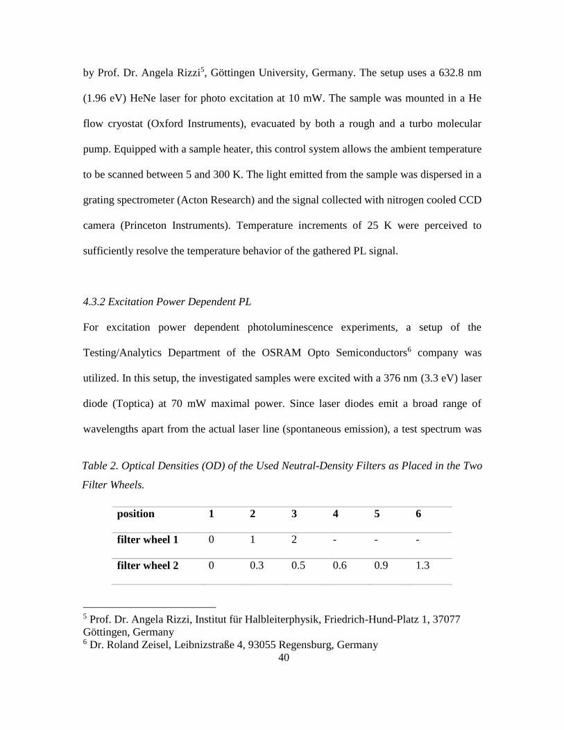
40
by Prof. Dr. Angela Rizzi5, Göttingen University, Germany. The setup uses a 632.8 nm
(1.96 eV) HeNe laser for photo excitation at 10 mW. The sample was mounted in a He
flow cryostat (Oxford Instruments), evacuated by both a rough and a turbo molecular
pump. Equipped with a sample heater, this control system allows the ambient temperature
to be scanned between 5 and 300 K. The light emitted from the sample was dispersed in a
grating spectrometer (Acton Research) and the signal collected with nitrogen cooled CCD
camera (Princeton Instruments). Temperature increments of 25 K were perceived to
sufficiently resolve the temperature behavior of the gathered PL signal.
4.3.2 Excitation Power Dependent PL
For excitation power dependent photoluminescence experiments, a setup of the
Testing/Analytics Department of the OSRAM Opto Semiconductors6 company was
utilized. In this setup, the investigated samples were excited with a 376 nm (3.3 eV) laser
diode (Toptica) at 70 mW maximal power. Since laser diodes emit a broad range of
wavelengths apart from the actual laser line (spontaneous emission), a test spectrum was
5 Prof. Dr. Angela Rizzi, Institut für Halbleiterphysik, Friedrich-Hund-Platz 1, 37077
Göttingen, Germany 6 Dr. Roland Zeisel, Leibnizstraße 4, 93055 Regensburg, Germany
Table 2. Optical Densities (OD) of the Used Neutral-Density Filters as Placed in the Two
Filter Wheels.
position 1 2 3 4 5 6
filter wheel 1 0 1 2 - - -
filter wheel 2 0 0.3 0.5 0.6 0.9 1.3
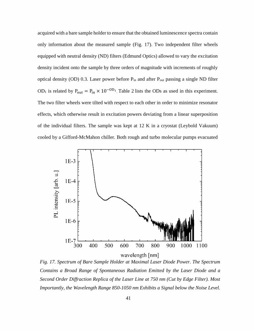
41
acquired with a bare sample holder to ensure that the obtained luminescence spectra contain
only information about the measured sample (Fig. 17). Two independent filter wheels
equipped with neutral density (ND) filters (Edmund Optics) allowed to vary the excitation
density incident onto the sample by three orders of magnitude with increments of roughly
optical density (OD) 0.3. Laser power before Pin and after Pout passing a single ND filter
OD1 is related by Pout = Pin × 10−OD1. Table 2 lists the ODs as used in this experiment.
The two filter wheels were tilted with respect to each other in order to minimize resonator
effects, which otherwise result in excitation powers deviating from a linear superposition
of the individual filters. The sample was kept at 12 K in a cryostat (Leybold Vakuum)
cooled by a Gifford-McMahon chiller. Both rough and turbo molecular pumps evacuated
Fig. 17. Spectrum of Bare Sample Holder at Maximal Laser Diode Power. The Spectrum
Contains a Broad Range of Spontaneous Radiation Emitted by the Laser Diode and a
Second Order Diffraction Replica of the Laser Line at 750 nm (Cut by Edge Filter). Most
Importantly, the Wavelength Range 850-1050 nm Exhibits a Signal below the Noise Level.
42
the cryostat. A grating spectrometer (Instrument Systems) separated different spectral
contributions of the light emitted by the sample and projected it onto a CCD camera to
record the obtained spectra. As the used type of spectrometer acquires data always for the
entire detectable wavelength range, the intense laser peak was attenuated by a 376 nm edge
filter (blocks light with wavelength < 376 nm) in order to prevent the CCD camera from
being overexposed. [54]
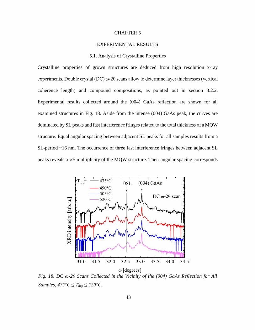
43
CHAPTER 5
EXPERIMENTAL RESULTS
5.1. Analysis of Crystalline Properties
Crystalline properties of grown structures are deduced from high resolution x-ray
experiments. Double crystal (DC) ω-2θ scans allow to determine layer thicknesses (vertical
coherence length) and compound compositions, as pointed out in section 3.2.2.
Experimental results collected around the (004) GaAs reflection are shown for all
examined structures in Fig. 18. Aside from the intense (004) GaAs peak, the curves are
dominated by SL peaks and fast interference fringes related to the total thickness of a MQW
structure. Equal angular spacing between adjacent SL peaks for all samples results from a
SL-period ~16 nm. The occurrence of three fast interference fringes between adjacent SL
peaks reveals a ×5 multiplicity of the MQW structure. Their angular spacing corresponds
Fig. 18. DC ω-2θ Scans Collected in the Vicinity of the (004) GaAs Reflection for All
Samples, 475°C ≤ Tdep ≤ 520°C.
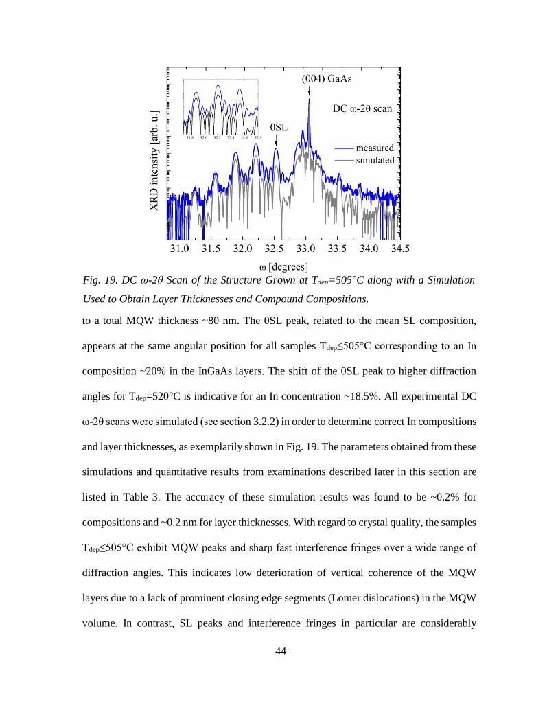
44
to a total MQW thickness ~80 nm. The 0SL peak, related to the mean SL composition,
appears at the same angular position for all samples Tdep≤505°C corresponding to an In
composition ~20% in the InGaAs layers. The shift of the 0SL peak to higher diffraction
angles for Tdep=520°C is indicative for an In concentration ~18.5%. All experimental DC
ω-2θ scans were simulated (see section 3.2.2) in order to determine correct In compositions
and layer thicknesses, as exemplarily shown in Fig. 19. The parameters obtained from these
simulations and quantitative results from examinations described later in this section are
listed in Table 3. The accuracy of these simulation results was found to be ~0.2% for
compositions and ~0.2 nm for layer thicknesses. With regard to crystal quality, the samples
Tdep≤505°C exhibit MQW peaks and sharp fast interference fringes over a wide range of
diffraction angles. This indicates low deterioration of vertical coherence of the MQW
layers due to a lack of prominent closing edge segments (Lomer dislocations) in the MQW
volume. In contrast, SL peaks and interference fringes in particular are considerably
Fig. 19. DC ω-2θ Scan of the Structure Grown at Tdep=505°C along with a Simulation
Used to Obtain Layer Thicknesses and Compound Compositions.
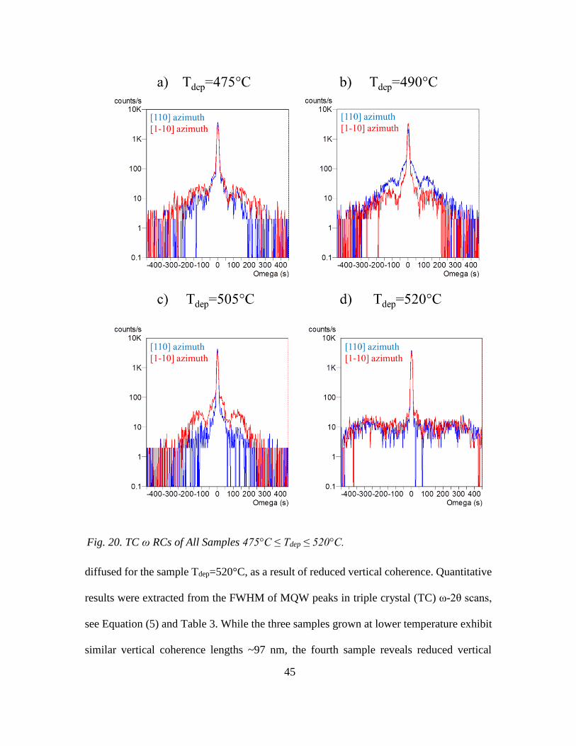
45
diffused for the sample Tdep=520°C, as a result of reduced vertical coherence. Quantitative
results were extracted from the FWHM of MQW peaks in triple crystal (TC) ω-2θ scans,
see Equation (5) and Table 3. While the three samples grown at lower temperature exhibit
similar vertical coherence lengths ~97 nm, the fourth sample reveals reduced vertical
Fig. 20. TC ω RCs of All Samples 475°C ≤ Tdep ≤ 520°C.
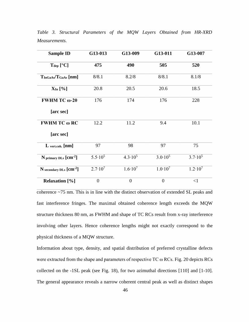
46
coherence ~75 nm. This is in line with the distinct observation of extended SL peaks and
fast interference fringes. The maximal obtained coherence length exceeds the MQW
structure thickness 80 nm, as FWHM and shape of TC RCs result from x-ray interference
involving other layers. Hence coherence lengths might not exactly correspond to the
physical thickness of a MQW structure.
Information about type, density, and spatial distribution of preferred crystalline defects
were extracted from the shape and parameters of respective TC ω RCs. Fig. 20 depicts RCs
collected on the -1SL peak (see Fig. 18), for two azimuthal directions [110] and [1-10].
The general appearance reveals a narrow coherent central peak as well as distinct shapes
Table 3. Structural Parameters of the MQW Layers Obtained from HR-XRD
Measurements.
Sample ID G13-013 G13-009 G13-011 G13-007
Tdep [°C] 475 490 505 520
TInGaAs/TGaAs [nm] 8/8.1 8.2/8 8/8.1 8.1/8
XIn [%] 20.8 20.5 20.6 18.5
FWHM TC ω-2θ
[arc sec]
176 174 176 228
FWHM TC ω RC
[arc sec]
12.2 11.2 9.4 10.1
L vert.coh. [nm] 97 98 97 75
N primary DLs [cm-2] 5.5∙105 4.3∙105 3.0∙105 3.7∙105
N secondary DLs [cm-2] 2.7∙107 1.6∙107 1.0∙107 1.2∙107
Relaxation [%] 0 0 0 <1
47
and extents of diffuse scattering. The linewidth of the narrow coherent peak is used to
estimate the density of primary 60° dislocation loops (DL). A trend of increasing primary
DL density with decreasing deposition temperature can be extracted from Tdep=505°C on.
The significance of this trend is, however, limited as each value lies within an estimated
error range of the other respective densities. Pronounced interference wings (at Δω≈±150
arc sec) in the diffuse scattering range for the structures Tdep≤505°C suggest lateral
ordering of secondary 60° dislocation loops in the volume. Their density can be estimated
from the width of the base below the narrow coherent peaks. Like the primary DL density,
the density of secondary DLs exhibits an increase with decreasing deposition temperature
from Tdep=505°C on. Particular differences in pronunciation of interference wings and
diffuse scattering base depending on the azimuthal angle can be observed for each sample,
respectively. The RC for sample Tdep=505°C measured in [110] azimuth reveals the lowest
amount of diffuse scattering among all curves. Crystal deterioration observes a minimum
in this sample along the [110] direction. In contrast to pronounced interference wings, the
RC of the structure Tdep=520°C shows a broad range of diffuse scattering contributions.
Crystalline deteriorations are hence assigned to comparatively small defects with a more
isotropic spatial distribution in the volume. The azimuthal anisotropy is lifted.
Symmetrical ω-2θ/ω reciprocal space maps (RSM) collected around (004) GaAs
diffraction spot are depicted in Fig. 21. The samples grown at the three lowest temperatures
reveal narrow diffraction peaks elongated along the vertical diffraction vector. The peaks
are connected by a streaky surface truncation rod as a result of high vertical coherence. In
structure Tdep=475°C the surface truncation rod is slightly less pronounced, indicating
inferior vertical coherence as compare to the other two structures. All RSMs exhibit areas
48
of diffuse scattering in the vicinity of the coherent scattering spots. Weakest diffuse
scattering was found for Tdep=505°C with only faint scattering extending into lateral
diffraction direction, as a result of high crystalline quality. RSMs visually confirmed the
amount of diffuse scattering increases with reduced deposition temperature between
Tdep=505°C and Tdep=475°C.
On the contrary, the symmetric RSM of structure Tdep=520°C does not reveal a pronounced
surface truncation rod. The vertical coherence is considerably reduced when compared to
all the other three structures. Besides, the graph shows extensive areas of diffuse scattering,
indicating high crystalline deterioration with a broad range of length scales.
The extent of relaxation of initial elastic stress was inferred from asymmetrical ω-2θ/ω
RSMs collected around the (224) GaAs diffraction spot, Fig. 22. All RSMs are composed
of the coherent (224) GaAs spot (red bar) and a series of (224) SL peaks (black bar).
Diffraction peaks appear clear and narrow for the structures Tdep=490°C and Tdep=505°C,
or less intense (Tdep=475°C) and diffused (Tdep=520°C). Coinciding lateral positions for
(224) GaAs spot and (224) InGaAs – SL spots visually confirm a lack of relaxation in the
structures Tdep≤505°C. The number of created secondary DLs did not suffice to initiate
overall strain accommodation. In contrast, < 1% relaxation was observed in the sample
Tdep=520°C, along with wide areas of diffuse scattering.
The evaluation of several HR-XRD experiments, namely DC and TC ω-2θ scans, TC ω
RCs, and symmetrical as well as asymmetrical RSMs, reveals a coherent picture of
crystalline quality and defect creation in four examined structures. Deposition at
Tdep=505°C was identified as optimal temperature for epitaxial growth resulting in best

49
quality InGaAs layers with 20% In composition. Lower temperatures revealed a gradual
increase in 60° primary and secondary DL density, and a decrease in lateral and vertical
coherence. Lateral spatial ordering at these temperatures is contrasted by more isotropically
distributed defects for the structure grown above the optimal Tdep found. Such high
deposition temperature (Tdep=520°C) led to minimal vertical and lateral coherence, highest
crystal deterioration among the investigated samples, and initial stress relaxation.
50
Fig. 21. Symmetrical Reciprocal Space Maps for All Samples 475°C ≤ Tdep ≤ 520°C
Collected around the (004) 0 SL Spot of the MQW Structure. The 0SL Peak of the MQW
Structure Is Indicated by the Red Horizontal Bar, While the -1SL Peak Is Located on the
Black Horizontal Bar.
51
Fig. 22. Asymmetrical Reciprocal Space Maps for All Samples 475°C ≤ Tdep ≤ 520°C
Collected around the (224) GaAs Diffraction. The (224) GaAs Diffraction Spot Is Indicated
by the Red Horizontal Bar, While the (224) SL Peak of the MQW Structure Is Located on
the Black Horizontal Bar.
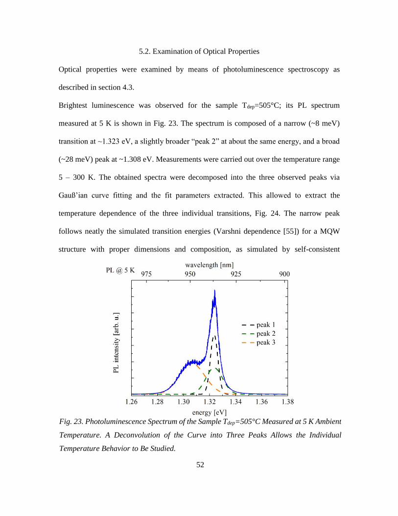
52
5.2. Examination of Optical Properties
Optical properties were examined by means of photoluminescence spectroscopy as
described in section 4.3.
Brightest luminescence was observed for the sample Tdep=505°C; its PL spectrum
measured at 5 K is shown in Fig. 23. The spectrum is composed of a narrow (~8 meV)
transition at ~1.323 eV, a slightly broader “peak 2” at about the same energy, and a broad
(~28 meV) peak at ~1.308 eV. Measurements were carried out over the temperature range
5 – 300 K. The obtained spectra were decomposed into the three observed peaks via
Gauß’ian curve fitting and the fit parameters extracted. This allowed to extract the
temperature dependence of the three individual transitions, Fig. 24. The narrow peak
follows neatly the simulated transition energies (Varshni dependence [55]) for a MQW
structure with proper dimensions and composition, as simulated by self-consistent
Fig. 23. Photoluminescence Spectrum of the Sample Tdep=505°C Measured at 5 K Ambient
Temperature. A Deconvolution of the Curve into Three Peaks Allows the Individual
Temperature Behavior to Be Studied.
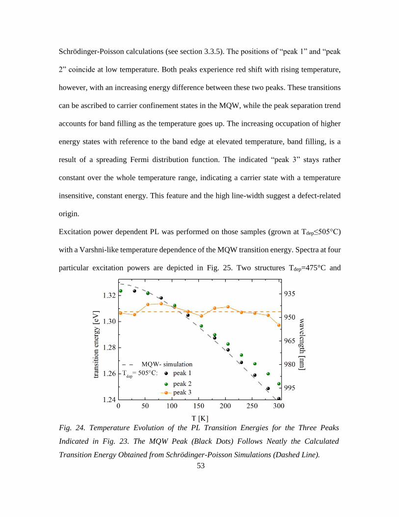
53
Schrödinger-Poisson calculations (see section 3.3.5). The positions of “peak 1” and “peak
2” coincide at low temperature. Both peaks experience red shift with rising temperature,
however, with an increasing energy difference between these two peaks. These transitions
can be ascribed to carrier confinement states in the MQW, while the peak separation trend
accounts for band filling as the temperature goes up. The increasing occupation of higher
energy states with reference to the band edge at elevated temperature, band filling, is a
result of a spreading Fermi distribution function. The indicated “peak 3” stays rather
constant over the whole temperature range, indicating a carrier state with a temperature
insensitive, constant energy. This feature and the high line-width suggest a defect-related
origin.
Excitation power dependent PL was performed on those samples (grown at Tdep≤505°C)
with a Varshni-like temperature dependence of the MQW transition energy. Spectra at four
particular excitation powers are depicted in Fig. 25. Two structures Tdep=475°C and
Fig. 24. Temperature Evolution of the PL Transition Energies for the Three Peaks
Indicated in Fig. 23. The MQW Peak (Black Dots) Follows Neatly the Calculated
Transition Energy Obtained from Schrödinger-Poisson Simulations (Dashed Line).

54
Tdep=490°C reveal a single prominent transition with weak energy dependence on
excitation power (~2 meV blueshift for depicted spectra) and weak sub-bandgap
luminescence. The energetic position deviates by 23 meV and 18 meV from the simulated
MQW transition value for the samples Tdep=475°C and Tdep=490°C, respectively. In both
cases the linewidth is about 10 meV (~7 nm). In contrast, the structure Tdep=505°C reveals
both the MQW state and prominent sub-bandgap transitions. At low excitation the intensity
of the sub-bandgap luminescence exceeds the one of the MQW peak, whereas its relative
intensity decreases with rising pumping level. This indicates a saturation of these optically
active sub-bandgap states with increasing generated carrier density, whereupon the
radiative recombination via the MQW states becomes relatively stronger. The sub-bandgap
transition was already found in the temperature dependent PL (compare Fig. 23 with
adequate excitation power 1 mW - red in Fig. 25). The linewidth of the MQW transition is
~10-12 meV (~9 nm). The narrow linewidths of all three MQW structures indicate high
material quality7.
7 Compare to 6.3 meV in [13]: 5K spectrum of InGaAs-single quantum well, XIn~26%,
thickness: 6.8 nm
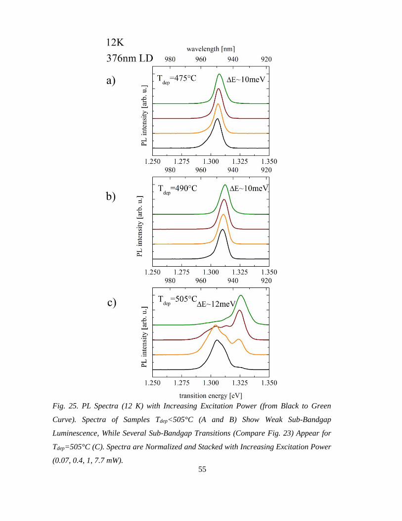
55
Fig. 25. PL Spectra (12 K) with Increasing Excitation Power (from Black to Green
Curve). Spectra of Samples Tdep<505°C (A and B) Show Weak Sub-Bandgap
Luminescence, While Several Sub-Bandgap Transitions (Compare Fig. 23) Appear for
Tdep=505°C (C). Spectra are Normalized and Stacked with Increasing Excitation Power
(0.07, 0.4, 1, 7.7 mW).
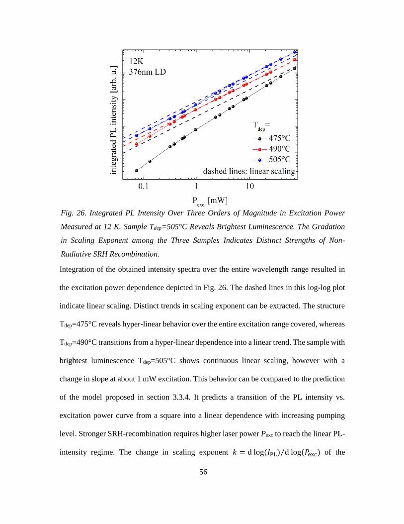
56
Integration of the obtained intensity spectra over the entire wavelength range resulted in
the excitation power dependence depicted in Fig. 26. The dashed lines in this log-log plot
indicate linear scaling. Distinct trends in scaling exponent can be extracted. The structure
Tdep=475°C reveals hyper-linear behavior over the entire excitation range covered, whereas
Tdep=490°C transitions from a hyper-linear dependence into a linear trend. The sample with
brightest luminescence Tdep=505°C shows continuous linear scaling, however with a
change in slope at about 1 mW excitation. This behavior can be compared to the prediction
of the model proposed in section 3.3.4. It predicts a transition of the PL intensity vs.
excitation power curve from a square into a linear dependence with increasing pumping
level. Stronger SRH-recombination requires higher laser power Pexc to reach the linear PL-
intensity regime. The change in scaling exponent 𝑘 = dlog(𝐼PL) dlog(𝑃exc)⁄ of the
Fig. 26. Integrated PL Intensity Over Three Orders of Magnitude in Excitation Power
Measured at 12 K. Sample Tdep=505°C Reveals Brightest Luminescence. The Gradation
in Scaling Exponent among the Three Samples Indicates Distinct Strengths of Non-
Radiative SRH Recombination.
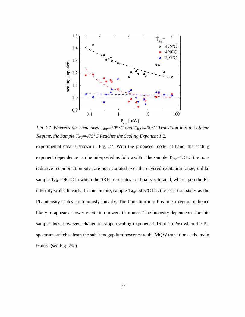
57
experimental data is shown in Fig. 27. With the proposed model at hand, the scaling
exponent dependence can be interpreted as follows. For the sample Tdep=475°C the non-
radiative recombination sites are not saturated over the covered excitation range, unlike
sample Tdep=490°C in which the SRH trap-states are finally saturated, whereupon the PL
intensity scales linearly. In this picture, sample Tdep=505°C has the least trap states as the
PL intensity scales continuously linearly. The transition into this linear regime is hence
likely to appear at lower excitation powers than used. The intensity dependence for this
sample does, however, change its slope (scaling exponent 1.16 at 1 mW) when the PL
spectrum switches from the sub-bandgap luminescence to the MQW transition as the main
feature (see Fig. 25c).
Fig. 27. Whereas the Structures Tdep=505°C and Tdep=490°C Transition into the Linear
Regime, the Sample Tdep=475°C Reaches the Scaling Exponent 1.2.
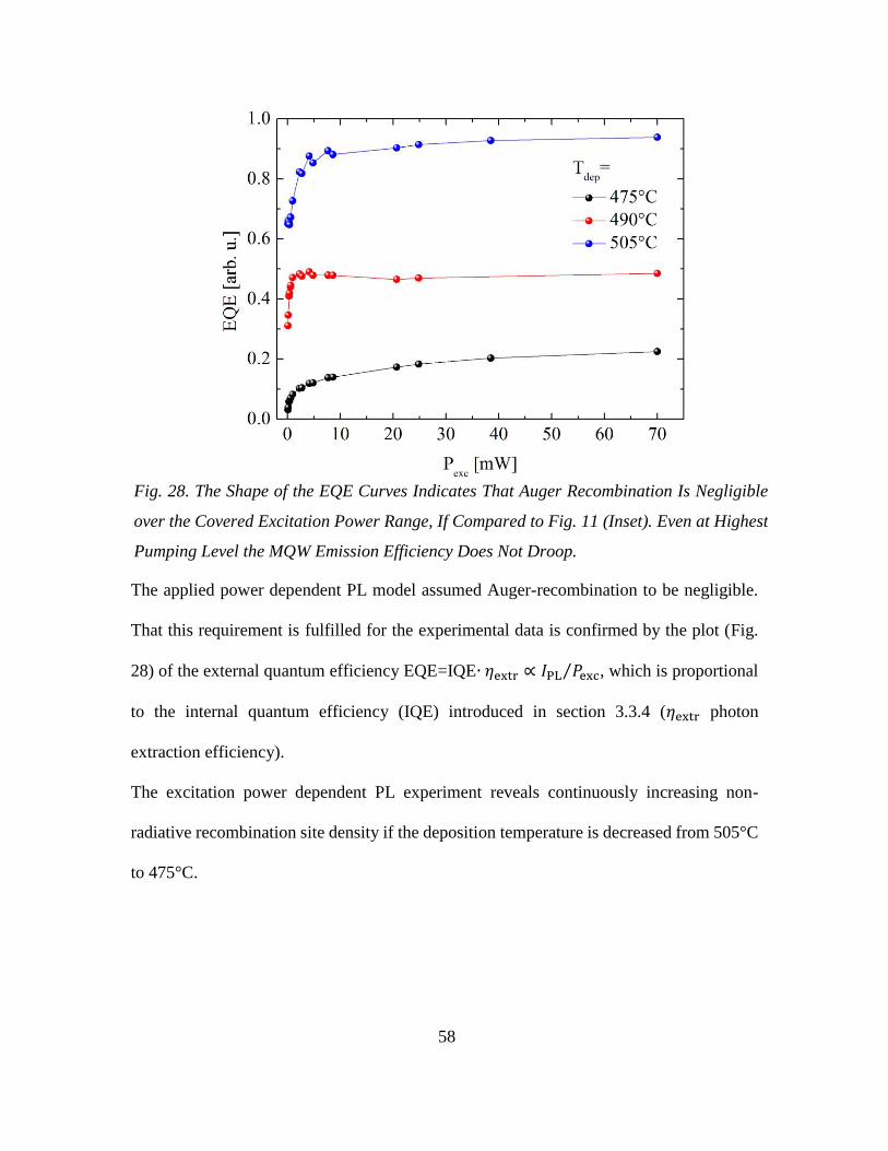
58
The applied power dependent PL model assumed Auger-recombination to be negligible.
That this requirement is fulfilled for the experimental data is confirmed by the plot (Fig.
28) of the external quantum efficiency EQE=IQE∙ 𝜂extr ∝ 𝐼PL 𝑃exc⁄ , which is proportional
to the internal quantum efficiency (IQE) introduced in section 3.3.4 (𝜂extr photon
extraction efficiency).
The excitation power dependent PL experiment reveals continuously increasing non-
radiative recombination site density if the deposition temperature is decreased from 505°C
to 475°C.
Fig. 28. The Shape of the EQE Curves Indicates That Auger Recombination Is Negligible
over the Covered Excitation Power Range, If Compared to Fig. 11 (Inset). Even at Highest
Pumping Level the MQW Emission Efficiency Does Not Droop.
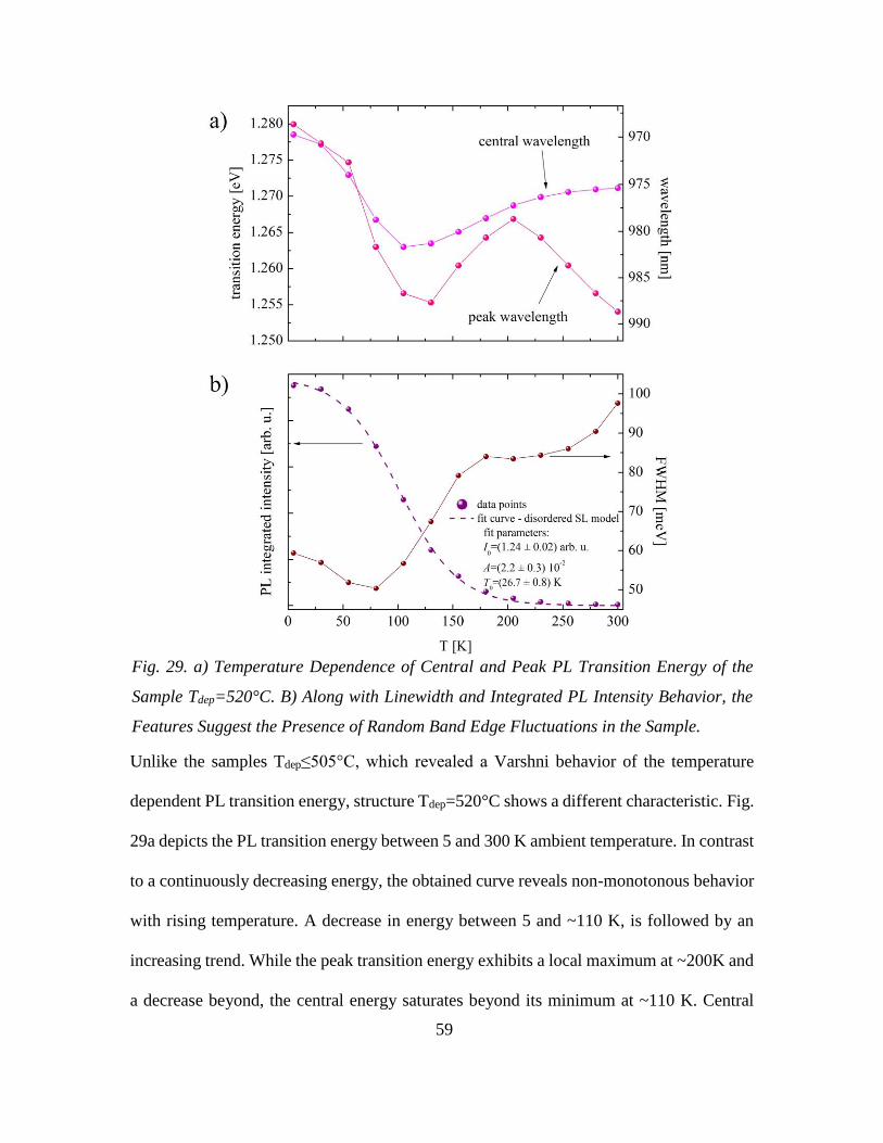
59
Unlike the samples Tdep≤505°C, which revealed a Varshni behavior of the temperature
dependent PL transition energy, structure Tdep=520°C shows a different characteristic. Fig.
29a depicts the PL transition energy between 5 and 300 K ambient temperature. In contrast
to a continuously decreasing energy, the obtained curve reveals non-monotonous behavior
with rising temperature. A decrease in energy between 5 and ~110 K, is followed by an
increasing trend. While the peak transition energy exhibits a local maximum at ~200K and
a decrease beyond, the central energy saturates beyond its minimum at ~110 K. Central
Fig. 29. a) Temperature Dependence of Central and Peak PL Transition Energy of the
Sample Tdep=520°C. B) Along with Linewidth and Integrated PL Intensity Behavior, the
Features Suggest the Presence of Random Band Edge Fluctuations in the Sample.

60
and peak energy reveal similar values below 80 K. The difference between those energy
values does not increase monotonously, as expected from band filling process, but instead
exhibits a local minimum at ~200 K. The temperature dependent PL energy trend appears
detached from the simulated Varshni dependence (Fig. 24).
The PL linewidth (Fig. 29b) is even at 5 K comparatively high (~60 meV). Increasing
ambient temperature first leads to a decrease in linewidth until ~80 K and is then followed
by increasing values. While the linewidth exhibits a nearly constant value between 180 and
230 K, it increases again beyond.
Both, the S-shape behavior of the PL transition energy and the non-monotonous linewidth
dependence suggest the presence of random band edge fluctuations, which lead to
localization of generated carriers in local energy minima. This mechanism of carrier
localization in local energy minima was previously described in amorphous structures,
disordered superlattices [57], and InGaN QWs with composition fluctuations [56, 58]. The
Fig. 30. Illustration of How Carrier Localization in Local Energy Minima May Influence
Temperature Dependence of PL Transition Energy and Linewidth. [56]
61
escape of carriers from local minima and their redistribution is a temperature activated
process (Fig. 30), which results in the shown characteristic features [58]. The temperature
dependence of the integrated PL intensity IPL has been described by [57, 58]
where T0 the characteristic temperature corresponding to the energy depth of localized
states from a mobility edge, t is the tunneling factor and I0 is the luminescence intensity in
the low-temperature limit. This formula has been fitted to the experimental data as shown
in Fig. 29b. The fit resulted in low statistical errors between 1 and 14% and high correlation
indicated by a coefficient of determination R2 of 0.9993. The good fit with the model
proposed for carrier localization stresses the previously suggested random band edge
fluctuations in sample Tdep=520°C.
The evaluation of several PL experiments, namely temperature dependent and excitation
power dependent PL measurements reveals a coherent picture of the optical properties and
defect creation in four examined structures. Deposition at Tdep=505°C was identified as
optimal temperature for epitaxial growth resulting in best optical properties for InGaAs
layers with 20% In composition. Lower temperatures revealed a gradual increase in non-
radiative recombination strength. Varshni-like transition energy dependence for these
deposition temperatures is contrasted by S-shape behavior at elevated deposition
temperature indicating localization of generated carriers in local energy minima. Such high
deposition temperature (Tdep=520°C) led to random band edge fluctuations, most likely
related to InGaAs decomposition.
𝐼PL =𝐼0
1 + 𝑡 exp(𝑇/𝑇0) (9)
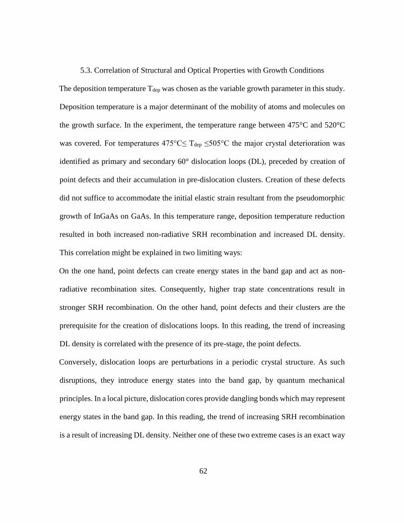
62
5.3. Correlation of Structural and Optical Properties with Growth Conditions
The deposition temperature Tdep was chosen as the variable growth parameter in this study.
Deposition temperature is a major determinant of the mobility of atoms and molecules on
the growth surface. In the experiment, the temperature range between 475°C and 520°C
was covered. For temperatures 475°C≤ Tdep ≤505°C the major crystal deterioration was
identified as primary and secondary 60° dislocation loops (DL), preceded by creation of
point defects and their accumulation in pre-dislocation clusters. Creation of these defects
did not suffice to accommodate the initial elastic strain resultant from the pseudomorphic
growth of InGaAs on GaAs. In this temperature range, deposition temperature reduction
resulted in both increased non-radiative SRH recombination and increased DL density.
This correlation might be explained in two limiting ways:
On the one hand, point defects can create energy states in the band gap and act as non-
radiative recombination sites. Consequently, higher trap state concentrations result in
stronger SRH recombination. On the other hand, point defects and their clusters are the
prerequisite for the creation of dislocations loops. In this reading, the trend of increasing
DL density is correlated with the presence of its pre-stage, the point defects.
Conversely, dislocation loops are perturbations in a periodic crystal structure. As such
disruptions, they introduce energy states into the band gap, by quantum mechanical
principles. In a local picture, dislocation cores provide dangling bonds which may represent
energy states in the band gap. In this reading, the trend of increasing SRH recombination
is a result of increasing DL density. Neither one of these two extreme cases is an exact way
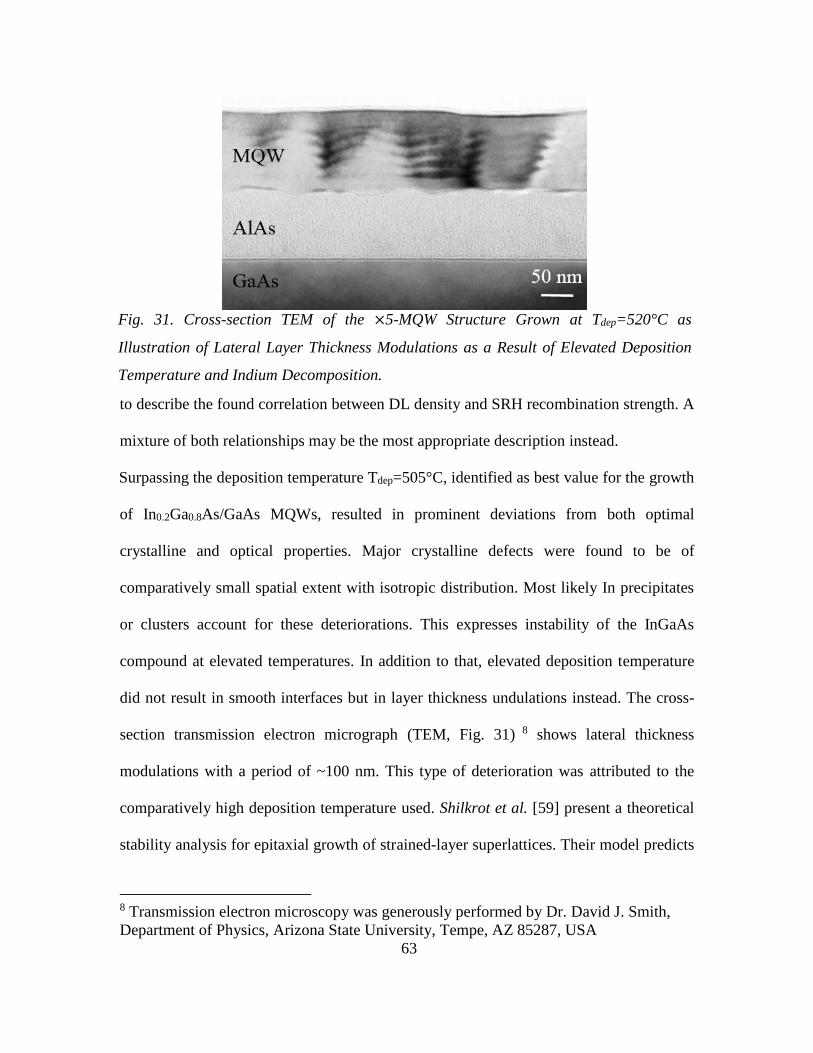
63
to describe the found correlation between DL density and SRH recombination strength. A
mixture of both relationships may be the most appropriate description instead.
Surpassing the deposition temperature Tdep=505°C, identified as best value for the growth
of In0.2Ga0.8As/GaAs MQWs, resulted in prominent deviations from both optimal
crystalline and optical properties. Major crystalline defects were found to be of
comparatively small spatial extent with isotropic distribution. Most likely In precipitates
or clusters account for these deteriorations. This expresses instability of the InGaAs
compound at elevated temperatures. In addition to that, elevated deposition temperature
did not result in smooth interfaces but in layer thickness undulations instead. The cross-
section transmission electron micrograph (TEM, Fig. 31) 8 shows lateral thickness
modulations with a period of ~100 nm. This type of deterioration was attributed to the
comparatively high deposition temperature used. Shilkrot et al. [59] present a theoretical
stability analysis for epitaxial growth of strained-layer superlattices. Their model predicts
8 Transmission electron microscopy was generously performed by Dr. David J. Smith,
Department of Physics, Arizona State University, Tempe, AZ 85287, USA
Fig. 31. Cross-section TEM of the ×5-MQW Structure Grown at Tdep=520°C as
Illustration of Lateral Layer Thickness Modulations as a Result of Elevated Deposition
Temperature and Indium Decomposition.
64
a change from stable growth resulting in flat interfaces, to a regime in which the surface is
unstable with respect to the growth of perturbations once a critical surface diffusivity is
exceeded. Fig. 32 depicts an illustration of the multilayer film morphology the authors
predict for elevated surface diffusivity. Such modulations in the MQW layers cause local
fluctuations in the averaged composition.
The two observed instabilities, namely the InGaAs decomposition and structural instability
with respect to layer undulations, represent origins of modulations in the local band edge
in the MQW volume. Band edge fluctuations are the cause for the localization of charge
carriers in local energy minima. The occurrence of the carrier localization mechanism was
observed in the structure Tdep=520°C as a prominent feature in the optical properties. The
observed optical properties are hence a direct result of the structural and crystalline
features.
InGaAs/GaAs MQW structures reveal correlation between their crystal quality and optical
properties with used MBE deposition temperature in the range between 475°C and 520°C.
Fig. 32. Multilayer Film Morphology of an Out-Of-Phase Instability. [59]
65
CHAPTER 6
CONCLUSIONS
In this thesis, the epitaxial growth of InGaAs/GaAs MQW structures at the initial stage of
defect creation was studied. The work correlates crystalline and optical properties of grown
structures with the deposition temperature used during MBE growth.
Suitable techniques and metrics for the examination of crystalline and optical properties
were chosen and the evaluation of experimental data established. In particular, a model for
the analysis of the strength of non-radiative SRH recombination on the basis of excitation
power dependent PL spectra was proposed. The model assumes charge carriers to be
spatially confined in an active region upon generation by an external light source. The
dependence of the luminescence intensity is related to the laser power in an excitation limit,
in which only SRH and radiative recombination need to be considered. The transition from
square into linear scaling is pivotal in the assessment of non-radiative SRH recombination
strength.
Four InGaAs/GaAs MQW structures with 20% In composition were epitaxially grown at
deposition temperatures between 475°C and 520°C. The grown samples were characterized
by means of HR-XRD and PL. Deposition at Tdep=505°C was identified as optimal value
for the growth at 20% In composition. For the temperature range 475°C ≤ Tdep ≤505°C,
primary and secondary 60° dislocation loops were identified as main crystalline
deterioration. The density of both kinds of mixed-type dislocations increased continuously
with decreasing deposition temperature. Likewise non-radiative SRH recombination
became more dominant as growth temperature was reduced. Hence, crystalline and optical
properties exhibit a correlation with the used growth condition.

66
Exceeding the optimal value Tdep=505°C revealed two kinds of instabilities at Tdep=520°C.
Material instability led to InGaAs decomposition and structural instability resulted in layer
thickness undulations. Both features represent causes for fluctuations of the local bandgap,
which may affect optical properties. The experimental optical analysis suggests the
localization of charge carriers in local energy minima. These local energy minima are
hence assumed to result from the fluctuations in the local bandgap. The found material and
morphology instabilities can thus be directly correlated with the optical properties.
The experiments on growth and characterization of InGaAs/GaAs MQWs reveal an
optimal deposition temperature range for each In composition. Obtained structures are
characterized by high crystal perfection and best optical response.
For device and growth process design, it is of special importance to consider correlations
between physical properties, such as the optical response, and crystal perfection as
dependent on growth conditions. Suboptimal growth conditions can easily deteriorate
material quality and degrade final device performance. The results allow to optimize
structure design and epitaxial growth of MQWs for various device applications.
67
REFERENCES
[1] K. Lasswitz. Wirklichkeit – Beiträge zum Weltverständnis. Verlag von Emil Feber,
1900.
[2] Z.I. Alferov. Nobel Lecture: The double heterostructure concept and its
applications in physics, electronics, and technology. Reviews of Modern Physics
73(3):767-782, 2001.
[3] H. Kroemer. Theory of wide-gap emitter for transistors. Proceedings of the IRE
45(11):1535-5137, 1957.
[4] H. Kroemer. A proposed class of hetero-junction injection lasers. Proceedings of
the IEEE 51(12):1782-1783, 1963.
[5] R. Dingle, W. Wiegmann, C.H. Henry. Quantum states of confined carriers in very
thin AlxGa1-xAs-GaAs-AlxGa1-xAs heterostructures. Physical Review Letters
33(14):827-830, 1974.
[6] H. Kroemer. Noble Lecture: Quasielectric fields and band offsets: teaching
electrons new tricks. Reviews of Modern Physics 73(3):783-793, 2001.
[7] M. Quillec, L. Goldstein, G. Le Roux, J. Burgeat, J. Primot. Growth conditions and
characterization of InGaAs/GaAs strained layers superlattices. Journal of Applied
Physics 55(8):2904-2909, 1984.
[8] B. Grandidier, H. Chen, R.M. Feenstra, D.T. McInturff, P.W. Juodawlkis, S.E.
Ralph. Scanning tunneling microscopy and spectroscopy of arsenic antisites in low
temperature grown InGaAs. Applied Physics Letters 74(10):1439-1441, 1999.
[9] J.F. Klem, W.S. Fu, P.L. Gourley, E.D. Jones, T.M. Brennan, J.A. Lott. Role of
substrate threading dislocation density in relaxation of highly strained
InGaAs/GaAs quantum well structures. Applied Physics Letters 56(14):1350-1352,
1990.
68
[10] D.C. Bertolet, J.K. Hsu, K.M. Lau, E.S. Koteles, D. Owens. Exciton
photoluminescence linewidths in very narrow AlGaAs/GaAs and GaAs/InGaAs
quantum wells. Journal of Applied Physics 64(11):6562-6564, 1988.
[11] G.W. Pickrell, K.L. Chang, J.H. Epple, K.Y. Cheng, K.C. Hsieh. Growth of low-
defect density In0.25Ga0.75As on GaAs by molecular beam epitaxy. Journal of
Vacuum Science and Technology B 18(6):2611-2614, 2000.
[12] A. Madhukar, K.C. Rajkumar, L. Chen, S. Guha, K. Kaviani, R. Kapre. Realization
of low defect density, ultrathick, strained InGaAs/GaAs multiple quantum well
structures via growth on patterned GaAs(100) substrates. Applied Physics Letters
57(19):2007-2009, 1990.
[13] R.L.S. Devine. PL characterization of InGaAs/GaAs QW structures.
Semiconductor Science and Technology 3:1171-1176, 1988.
[14] J.W. Matthews, A.E. Blakeslee. Defects in epitaxial layers III. Preparation of
almost perfect multilayers. Journal of Crystal Growth 32(2):265-273, 1976.
[15] B. Elman, E.S. Koteles, P. Melman, C. Jagannath, J. Lee, D. Dugger. In situ
measurements of critical layer thickness and optical studies of InGaAs quantum
wells grown on GaAs substrates. Applied Physics Letters 55(16):1659-1661, 1989.
[16] E.A. Fitzgerald, D.G. Ast, P.D. Kirchner, G.D. Pettit, J.M. Woodall. Structure and
recombination in InGaAs/GaAs heterostructures. Journal of Applied Physics
63(3):693-703, 1988.
[17] J. Zou, D.J.H. Cockayne. Lomer-Cottrell misfit dislocations in [001]
In0.2Ga0.8As/GaAs single heterostructures. Applied Physics Letters 69(8):1083-
1085, 1996.
[18] J.W. Matthews, A.E. Blakeslee. Defects in epitaxial multilayers I. Misfit
dislocations. Journal of Crystal Growth 27:118-125, 1974.
69
[19] K.J. Beernink, P.K. York, J.J. Coleman, R.G. Waters, J. Kim, C.M. Wayman.
Characterization of InGaAs-GaAs strained-layer lasers with quantum wells near
critical thickness. Applied Physics Letters 55(21):2167-2169, 1989.
[20] J.F. Geisz, S. Kurtz, M.W. Wanlass, J.S. Ward, A. Duda, D.J. Friedman, J.M.
Olson, W.E. McMahon, T.E. Moriarty, J.T. Kiehl. High-efficiency
GaInP/GaAs/InGaAs triple-junction solar cells grown inverted with a metamorphic
bottom junction. Applied Physics Letters 91:23502-1 – 23502-3, 2007.
[21] K. Barnham, I. Ballard, J. Connolly, N. Ekins-Daukes, B. Kluftinger, J. Nelson, C.
Rohr. Quantum Well Solar Cells. Physica E 14:27-36, 2002.
[22] C.B. Honsberg, S.P. Bremner, R. Corkish. Design trade-offs and rules for multiplex
energy level solar cells. Physica E 14:136-141, 2002.
[23] A. Freundlich, G.K. Vijaya, A. Mehrotra. Superlattice intermediate band solar cell
with resonant upper-conduction-band assisted photo-absorption and carrier
extraction. Proceedings of 39th IEEE PVSC 1635-1638, 2013.
[24] C.Z. Ning. Semiconductor nanolasers. Physica Status Solidi B 247(4):774-788,
2010.
[25] M.T. Hill. Status and prospects for metallic and plasmonic nano-lasers. Journal of
the Optical Society of America B 27(11):B36-B44, 2010.
[26] K. Ding, Z.C. Liu, L.J. Yin, M.T. Hill, M.J.H. Marell, P.J. van Veldhoven, R.
Nöetzel, C.Z. Ning. Room-temperature continuous wave lasing in deep-
subwavelength metallic cavities under electrical injection. Physical Review B
85:041301-1 – 041301-5, 2012.
[27] K. Ploog. Molecular beam epitaxy of III-V compounds: Technology and growth
process. Annual Review of Materials Research 11:171-210, 1981.
[28] H. Ibach, H. Lüth. Solid State Physics. Springer, 2003.
70
[29] M.A. Herman, W. Richter, H. Sitter. Epitaxy: Physical principles and technical
implementation. Springer, 2004.
[30] B. Hillebrands. “Molecular beam epitaxy – Technische Universität Kaiserslautern”.
http://www.physik.uni-kl.de/hillebrands/research/methods/molecular-beam-
epitaxy/ accessed July 2014.
[31] H. Föll, B. Koblesen. Agglomerate von Zwischengitteratomen (Swirl-Defekte) in
Silizium – ihre Bedeutung für Grundlagenforschung und Technologie. Jahrbuch der
Akademie der Wissenschaften in Göttingen, Vandenhoeck & Ruprecht, 1976.
[32] N. Faleev, N. Sustersic, N. Bhargava, J. Kolodzey, A. Yu. Kazimirov, C. Honsberg.
Structural investigations of SiGe epitaxial layers grown by molecular beam epitaxy
on Si(001) and Ge(001) substrates: I-High resolution x-ray diffraction and x-ray
topography. Journal of Crystal Growth 365:44-53, 2013.
[33] N. Faleev, N. Sustersic, N. Bhargava, J. Kolodzey, S. Magonov, D.J. Smith, C.
Honsberg. Structural investigations of SiGe epitaxial layers grown by molecular
beam epitaxy on Si(001) and Ge(001) substrates: II-Transmission electron
microscopy and atomic force microscopy. Journal of Crystal Growth 365:35-43,
2013.
[34] S.P. Bremner, K.Y. Ban, N.N. Faleev, C.B. Honsberg, D.J. Smith. Impact of stress
relaxation in GaAsSb cladding layers on quantum dot creation in InAs/GaAsSb
structures grown on GaAs (001). Journal of Applied Physics 114(10):103511-1 –
103511-9, 2013.
[35] N.W. Ashcroft, N.D. Mermin. Solid State Physics. Brooks/Cole, 1976.
[36] U. Pitsch, V. Holy, T. Baumbach. High resolution x-ray scattering from thin films
and multilayers. Springer, 1999.
[37] C. Suryanarayana, M. Grant Norton. X-ray diffraction: A practical approach.
Plenum Press, 1998.
71
[38] P.F. Fewster. X-ray diffraction from low-dimensional structures. Semiconductor
Science and Technology 8(11):1915-1934, 1993.
[39] PANalytical manual. Epitaxy and Smoothfit – Software for the analysis of thin
layers. 2009.
[40] J.E. Ayers. The measurement of threading dislocation densities in semiconductor
crystals by x-ray diffraction. Journal of Crystal Growth 135:71-77, 1994.
[41] V.M. Kaganer, R. Köhler, M. Schmidtbauer, R. Opitz, B. Jenichen. X-ray
diffraction peaks due to misfit dislocations in heteroepitaxial structures. Physical
Review B 55(3):1793-1810, 1997.
[42] Ioffe Institute. “Band structure and carrier concentration of Gallium Arsenide
(GaAs)”. http://www.ioffe.ru/SVA/NSM/Semicond/GaAs/bandstr.html accessed
May 2014.
[43] W. Shockley, W.T. Read. Statistics of the recombination of holes and electrons.
Physical Review 87(5):835-842, 1952.
[44] R.N. Hall. Electron-Hole Recombination in Germanium. Physical Review
87(2):387, 1952.
[45] E. Rosencher, B. Vinter, P.G. Piva. Optoelectronics. Cambridge University Press,
2002.
[46] L. Meitner. Über die β-Strahl-Spektra und ihren Zusammenhang mit der γ-
Strahlung. Zeitschrift für Physik A. Hadrons and Nuclei 11:35-54, 1922.
[47] Z. Garbuzov. Reradiation effects, lifetimes and probabilities of band-to-band
transitions in direct A3B5 compounds of GaAs type. Journal of Luminescence
27:109-112, 1982.
72
[48] K.A. Bulashevich, S. Yu. Karpov. Is Auger recombination responsible for the
efficiency rollover in III-nitride light-emitting diodes? Physica Status Solidi C
5(6):2066-2069, 2008.
[49] P. Dirac. The quantum theory of the emission and absorption of radiation.
Proceedings of the Royal Society of London A 114:243-265, 1927.
[50] C. Weisbuch, B. Vinter. Quantum semiconductor structures – fundamentals and
applications. Academic Press, 1991.
[51] D.L. Smith, C. Mailhiot. Theory of semiconductor superlattice electronic structure.
Reviews of Modern Physics 62(1):173-234, 1990.
[52] P. Yu, M. Cardona. Fundamentals of semiconductors: physics and materials
properties. 3rd edition, Springer, 2001.
[53] S. Birner. “nextnano3 – next generation 3D nanodevice simulator”.
http://www.nextnano.com/nextnano3/index.htm accessed February 2013.
[54] B. Galler. Ladungsträger-Rekombination und -Transport in InGaN-basierenden
Leuchtdioden. PhD thesis, Freiburg University, 2014.
[55] Y.P. Varshni. Temperature dependence of the energy gap in semiconductors.
Physica 34(1):149-154, 1967.
[56] S.W. Feng, Y.C. Cheng, Y.Y. Chung, C. Yang, Y.S. Lin, C. Hsu, K.J. Ma, J.I. Chyi.
Impact of localized states on the recombination dynamics in InGaN/GaN quantum
well structures. Journal of Applied Physics 92(8):4441-4448, 2002.
[57] T. Yamamoto, M. Kasu, S. Noda, A. Sasaki. Photoluminescent properties and
optical absorption al AlAs/GaAs disordered superlattices. Journal of Applied
Physics 68(10):5318-5323, 1990.
[58] T.Y. Lin, J.C. Fan, Y.F. Chen. Effects of alloy fluctuations in InGaN epitaxial film.
Semiconductor Science and Technology 14:406-411, 1999.

73
[59] L.E. Shilkrot, D.J. Srolovitz, J. Tersoff. Morphology evolution during the growth
of strained-layer superlattices. Physical Review B 62(12):8397-8409, 2000.

74
BIOGRAPHICAL SKETCH
Matthias Karow was born in Gotha, Germany, where he completed his secondary education
in 2007 at Gymnasium Ernestinum with a major in Mathematics and Physics. He continued
his education in Physics, earning a Bachelors degree from Göttingen University in 2011
and beginning the pursuit of a Masters at the same institution with a focus on solid-state
and material physics. Upon receiving a Fulbright Scholarship, Matthias joined the QESST
ERC and the Electrical Engineering department at Arizona State University in 2012, from
which he earns a Masters degree in Summer 2014. He is a member of the HKN Engineering
Honor Society, IEEE, and the German Physical Society.


![Subcycle Nonlinear Response of Doped 4H Silicon Carbide ......instance GaAs, Si, Ge, and InGaAs [18-23]. In line with its potential for high-power THz applications, the possibility](https://img.pdfslide.us/doc/110x75/60df2e31b666e81ebd71dfd6/subcycle-nonlinear-response-of-doped-4h-silicon-carbide-instance-gaas-si.jpg)

![PROCEEDINGS OF SPIE...66360L Infrared photoconductivity of InGaAs/GaAs heterostructures with quantum dots [6636-20] V. Shashkin, V. Daniltsev, M. Drozdov, Y. Drozdov, V. Zakamov, A](https://img.pdfslide.us/doc/110x75/5f7f564ac2db2c4ae40102b1/proceedings-of-spie-66360l-infrared-photoconductivity-of-ingaasgaas-heterostructures.jpg)