Embed Size (px)
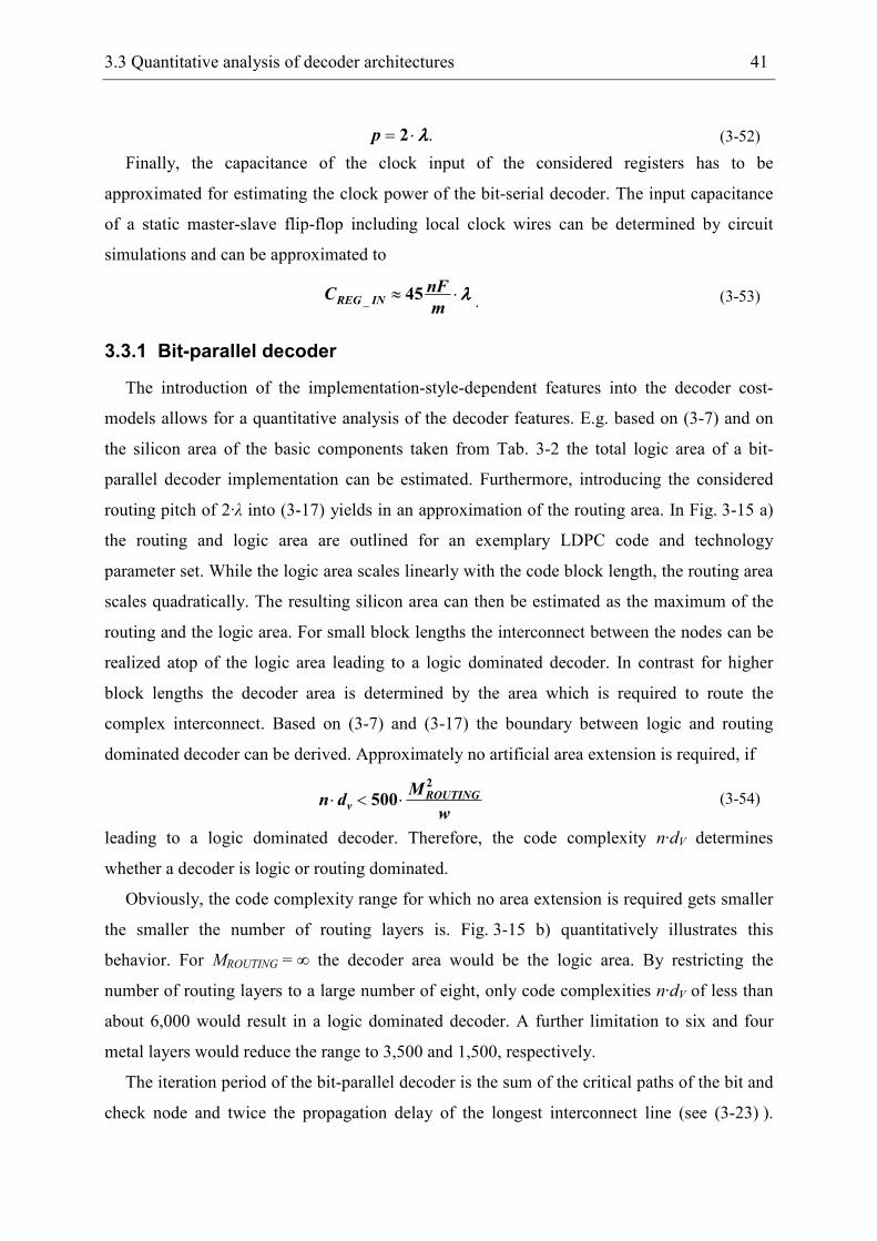
Citation preview
“Deep-Submicron Full-Custom VLSI-Design of Highly
Optimized High-Throughput Low-Latency LDPC Decoders”
Von der Fakultät für Elektrotechnik und Informationstechnik der Rheinisch-
Westfälischen Technischen Hochschule Aachen zur Erlangung des akademischen
Grades eines Doktors der Ingenieurwissenschaften genehmigte Dissertation
vorgelegt von
Diplom-Ingenieur
Matthias Korb
aus Arnsberg
Berichter: Universitätsprofessor Dr.-Ing. Tobias G. Noll
Universitätsprofessor Dr.-Ing. Norbert Wehn
Tag der mündlichen Prüfung: 18. Januar 2012
Diese Dissertation ist auf den Internetseiten der Hochschulbibliothek online verfügbar.

This thesis results from my work at the Institute of Electrical Engineering and Computer Systems at
the RWTH Aachen University which was partially supported by the German Research Foundation
(DFG) in its priority programme SPP1202.
I would like to express my deepest gratitude to Prof. Dr.-Ing. Tobias G. Noll for giving me the
opportunity to work in various interesting projects at the Institute of Electrical Engineering and
Computer Systems. I owe him many thanks for innumerable, inspiring discussions.
Secondly, I would like to thank Prof. Dr.-Ing. Norbert Wehn for his commitment and dedication
with regard to my coreferat.
I am very grateful to the colleagues at the Institute of Electrical Engineering and Computer Systems
for all the constructive discussions in the recent years.
Many thanks to my mother Edeltraud Korb and Ulf Preuß for their continuous encouragement and
support during my studies. Special thanks to Ulf Preuß who acquainted me with the field of
Electrical Engineering in the first place.
Finally, I would like to thank my wife Silvia, for everything.
Aachen, April 2012 Matthias Korb

Table of Contents
1 Motivation ...................................................................................................................... 5
2 Introduction .................................................................................................................... 9
2.1 Channel decoders ................................................................................................... 9
2.2 LDPC decoding algorithm ................................................................................... 11
2.3 Decoder architectures ........................................................................................... 15
2.4 Metrics of LDPC decoders................................................................................... 18
3 Generic ATE-cost models of LDPC decoders ............................................................. 21
3.1 Bit-parallel LDPC decoder................................................................................... 21
3.1.1 Logic area..................................................................................................... 22
3.1.2 Routing area ................................................................................................. 25
3.1.3 Iteration period ............................................................................................. 30
3.1.4 Energy per iteration...................................................................................... 31
3.2 Bit-serial LDPC decoder ...................................................................................... 33
3.3 Quantitative analysis of decoder architectures..................................................... 39
3.3.1 Bit-parallel decoder ...................................................................................... 41
3.3.2 Bit-serial decoder ......................................................................................... 43
3.3.3 Comparison of decoder architectures ........................................................... 44
3.4 Sum-Product decoder ........................................................................................... 46
4 Analysis of fixed-point decoding algorithm................................................................. 49
4.1 Hardware-accelerated HDL simulator ................................................................. 49
4.1.1 AWGN Channel ........................................................................................... 50
4.1.2 Decoder model ............................................................................................. 53
4.1.3 Hardware-accelerated HDL simulation........................................................ 54
4.2 Decoding performance analysis of fixed-point decoders ..................................... 55
4.2.1 Fixed-point effects on decoding performance.............................................. 55
4.2.2 Fixed-point Sum-Product decoder ............................................................... 56
4.2.3 Approximate Sum-Product decoder ............................................................. 59
4.2.4 Fixed-point Min-Sum decoder ..................................................................... 61
4.2.5 Approximate Min-Sum decoder................................................................... 64
5 Hardware-efficient decoder architectures .................................................................... 67
5.1 Area-efficient bit-parallel decoder architecture ................................................... 67
5.2 High-throughput partially bit-serial decoder architecture .................................... 74
5.2.1 Arithmetic optimization of nodes................................................................. 77
5.2.2 ATE-cost models.......................................................................................... 86
5.2.3 Digit-serial decoder architectures................................................................. 87
5.3 Quantitative architecture comparison................................................................... 88
6 Highly-optimized full-custom designed LDPC decoder.............................................. 91
6.1 Decoder implementation ...................................................................................... 91
6.2 Implementation of stopping criteria ..................................................................... 99
6.3 Benchmarking .................................................................................................... 103
7 Conclusion.................................................................................................................. 109
8 Abbreviations ............................................................................................................. 111
9 Bibliography............................................................................................................... 117
1 Motivation
The rapidly growing demand in data communication results in an increasing throughput
requirement of communication channels. As the bandwidth is typically limited the system has
to assure a communication very close to the theoretical Shannon limit to meet these
throughout specifications. In 1962 Gallager already presented a channel decoding algorithm
[1] which nearly achieves this theoretical limit [2] and allows for the best decoding
performance to this day. However, the complexity of this algorithm impeded an integration of
such decoders for a long time. Therefore, in the past Viterbi [3] or Turbo decoders [4] have
been adopted to various standards.
The first integrated LDPC decoder has been published 2002 by Blanksby and Howland [5].
From then on LDPC codes have been adopted to a wide range of communication standards
beginning from wire-bound communication systems like the IEEE 802.3an standard [6] and
the 1 GBit over powerline standard [7] to wireless communication systems like WiFi [8],
WiMax [9], DVB-S [10], and DTTB [11]. Recently LDPC codes have also been integrated in
read-write-channels of hard-disk drives [12].
The outstanding error correction performance of LDPC codes is due to an extensive
exchange of messages between the two building blocks of the receiver sided decoder. The
communication between these blocks highly affects the decoder features. The silicon area of
the decoder in [5] e.g. is highly increased to realize the complex interconnect between the two
block types leading to a utilization of the active silicon area of just 50 %. Since 2002 various
optimization techniques to reduce the impact of the interconnect have been proposed.
However, the benchmarking at the end of this work shows that for high-throughput
applications this reduction always consists of a trade-off between silicon area and throughput
and / or energy.
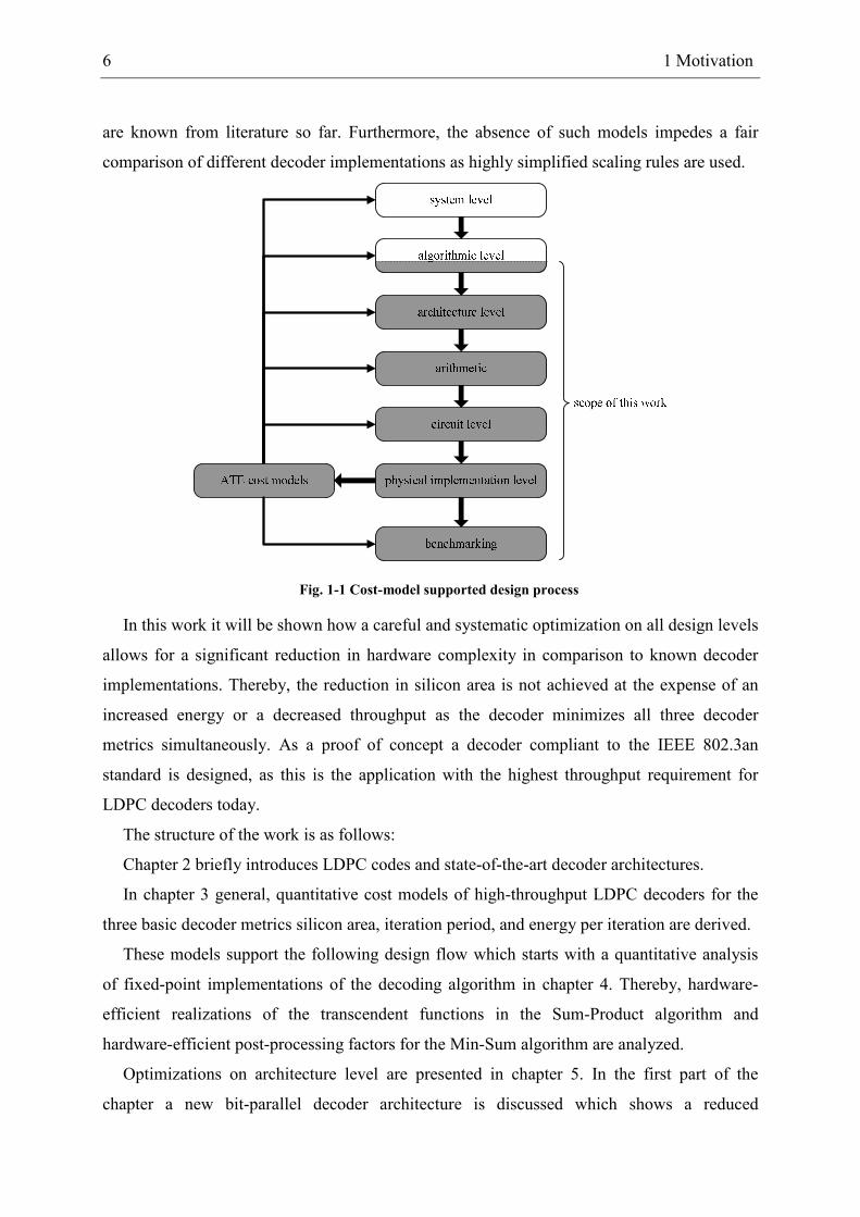
For a simultaneous reduction of all decoder features an optimization on all design levels
ranging from system level down to physical implementation level as illustrated in Fig. 1-1 is
mandatory. Thereby, on each design level the impact of different implementation options on
the resulting decoder features have to be estimated as accurate as possible to minimize the
probability of wrong decisions. For such a quantitative analysis accurate area-, timing-, and
energy-cost models are required. For less complex logic structures like e.g. finite-impulse-
response filters such generic cost models can be derived easily because they base on a simple
gate count. However, for LDPC decoders the influence of the global interconnect complicates
the derivation of general cost models. This might be the reason why no accurate cost models
6 1 Motivation
are known from literature so far. Furthermore, the absence of such models impedes a fair
comparison of different decoder implementations as highly simplified scaling rules are used.
Fig. 1-1 Cost-model supported design process
In this work it will be shown how a careful and systematic optimization on all design levels
allows for a significant reduction in hardware complexity in comparison to known decoder
implementations. Thereby, the reduction in silicon area is not achieved at the expense of an
increased energy or a decreased throughput as the decoder minimizes all three decoder
metrics simultaneously. As a proof of concept a decoder compliant to the IEEE 802.3an
standard is designed, as this is the application with the highest throughput requirement for
LDPC decoders today.
The structure of the work is as follows:
Chapter 2 briefly introduces LDPC codes and state-of-the-art decoder architectures.
In chapter 3 general, quantitative cost models of high-throughput LDPC decoders for the
three basic decoder metrics silicon area, iteration period, and energy per iteration are derived.
These models support the following design flow which starts with a quantitative analysis
of fixed-point implementations of the decoding algorithm in chapter 4. Thereby, hardware-
efficient realizations of the transcendent functions in the Sum-Product algorithm and
hardware-efficient post-processing factors for the Min-Sum algorithm are analyzed.
Optimizations on architecture level are presented in chapter 5. In the first part of the
chapter a new bit-parallel decoder architecture is discussed which shows a reduced
1 Motivation 7
interconnect impact on the silicon area. Furthermore, a systematic analysis of bit- and check-
node based architectures reveals a new partially bit-serial decoder architecture which
overcomes the drawbacks of today’s known architectures. This architecture is further
optimized on arithmetic level before ATE-cost models are derived which underline the
efficiency of this architecture.
In chapter 6 the optimizations performed on algorithm, architectural, and arithmetic level
are combined. The resulting decoder is realized in a deep-submicron CMOS technology using
a full-custom design flow for the LDPC code adopted in the IEEE 802.3an standard. Finally,
the decoder features are compared to other decoder implementations in a benchmarking.
Thereby, scaling rules have been derived based on the decoder cost-models of chapter 3 to
allow for a fair comparison.
Chapter 7 summarizes and concludes this work.

2 Introduction
Every communication channel, whether wired or wireless, is imperfect. Due to the
influences of other communication channels or other electromagnet noise sources the sent and
received information differ in general. To reduce the differences to a tolerable level channel
decoders are introduced into the transmission system. The underlying idea of channel
decoders is to add additional information called redundancy in the transmitter-sided channel
encoder. This redundancy can then be used in the receiver-sided channel decoder to cancel out
possible transmission errors.
2.1 Channel decoders
One major class of channel codes contains the so called block codes. For these codes the
information symbols generated by an information source are combined in blocks with a fixed
block length m as assumed in the simplified channel model in Fig. 2-1.
Fig. 2-1 Simplified model of communication channel with block code
In the channel encoder n-m redundant symbols are added to these m symbols leading to a
code blocks length of n. The more redundancy is added the higher is the probability that
communication errors can be corrected. However, if the bandwidth of the physical channel is
limited, an increasing number of redundancy symbols would reduce the effective bandwidth
which can be used for the information transfer. A metric for the error correction capability of
the code is the code rate
n
mR =.
(2-1)
A low code rate is an indicator of a large number of redundant symbols and, thus, a high
error correction potential.
For block codes the code word y of block length n can be generated by multiplying the
information word x of block length m with a generator matrix G as follows
Gxy ⋅= . (2-2)
10 2 Introduction
In the physical communication channel this code word gets distorted. Considering for
example additive white Gaussian noise (awgn) the received code word would be
wgnyy +='. (2-3)
Based on the introduced redundancy communication errors can be detected in the receiver
sided channel decoder. Therefore, the received code word is multiplied with a parity-check
matrix H. As the product of the generator matrix and the parity-check matrix is
0=⋅H'G
(2-4)
the multiplication of an error-free code word with the parity-check matrix would also be equal
to the zero vector:
0=⋅⋅=⋅ H'GxH'y' . (2-5)
Thereby, each of the m rows of H represents one parity check. The location of the one
entries in that row defines which symbols of the received code word are taking part in that
particular parity check. If the number of one entries per row and per column is constant, and,
therefore, each parity check bases on the same number of symbols and each symbol takes part
in the same number of parity checks, the matrix is called regular. Otherwise, it is called
irregular.
If the received code word is not error-free, the information which is generated during the
processing of the m parity checks can be used to correct the occurred transmission errors. This
basic principle is e.g. used in Turbo Codes introduced by Berrou, Glavieux and Thitimajshima
in 1993 [4]. The basic principle of a Turbo decoder is shown on the left side of Fig. 2-2. For
each of the n received noisy symbols a channel information L(ci) is calculated which indicates
the probability of a sent ‘1’ or ‘0’. Thereby, the sign is an estimation of the sent symbol and
the magnitude is an indicator for the reliability of the sign statement with a high magnitude
representing a high reliability.
In a Turbo decoder the information of all received symbols are fed into a soft-input-soft-
output (SISO) decoder which performs the parity checks defined by the matrix H and
calculates additional A-posteriori information L(ri) for each symbol i. These new information
are summed up with the channel information leading to a new estimation of the sent symbol
L(Qi).
Although the LDPC decoding algorithm was already introduced by Gallager in 1962 [1], it
can be seen as a modification or improvement of this Turbo principle. In contrast to the basic
Turbo decoder of Fig. 2-2, there are m SISO decoders in an LDPC decoder. Each of these m
decoders perform one of the m parity checks defined in the parity-check matrix and calculates
new A-posteriori information L(ri,j) for each participating symbol i. The A-posteriori
2.2 LDPC decoding algorithm 11
information for one symbol is combined with the channel information to derive a new
estimate of the received symbol. In the next iteration this sum is fed back to the SISO
decoders.
Fig. 2-2 Turbo- and LDPC- decoding principle
In LDPC decoders the single SISO decoders are called check nodes. The subsequent
combination of the A-priori and A-posteriori information is done in the so called bit nodes
leading to the so called Tanner Graph. The Tanner Graph for a simplified parity-check matrix
H is depicted in Fig. 2-3. The number of connections of each check node (bit node)
corresponds to the number of one entries in each row (column) of the parity-check matrix H
and is called the degree of the check node dC (bit node dV).
m rows
=
01101001
10100110
01101010
10011001
10010110
01010101
H
Fig. 2-3 Tanner Graph
2.2 LDPC decoding algorithm
In Fig. 2-4 a decoder loop consisting of one bit and one check node is depicted. For the
sake of clarity all the connections to other nodes are not drawn. At the beginning of the
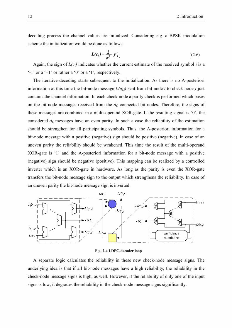
12 2 Introduction
decoding process the channel values are initialized. Considering e.g. a BPSK modulation
scheme the initialization would be done as follows
ii y'σ
)L(c ⋅=2
2.
(2-6)
Again, the sign of L(ci) indicates whether the current estimate of the received symbol i is a
‘-1’ or a ‘+1’ or rather a ‘0’ or a ‘1’, respectively.
The iterative decoding starts subsequent to the initialization. As there is no A-posteriori
information at this time the bit-node message L(qi,j) sent from bit node i to check node j just
contains the channel information. In each check node a parity check is performed which bases
on the bit-node messages received from the dC connected bit nodes. Therefore, the signs of
these messages are combined in a multi-operand XOR-gate. If the resulting signal is ‘0’, the
considered dC messages have an even parity. In such a case the reliability of the estimation
should be strengthen for all participating symbols. Thus, the A-posteriori information for a
bit-node message with a positive (negative) sign should be positive (negative). In case of an
uneven parity the reliability should be weakened. This time the result of the multi-operand
XOR-gate is ‘1’ and the A-posteriori information for a bit-node message with a positive
(negative) sign should be negative (positive). This mapping can be realized by a controlled
inverter which is an XOR-gate in hardware. As long as the parity is even the XOR-gate
transfers the bit-node message sign to the output which strengthens the reliability. In case of
an uneven parity the bit-node message sign is inverted.
--
Fig. 2-4 LDPC-decoder loop
A separate logic calculates the reliability in these new check-node message signs. The
underlying idea is that if all bit-node messages have a high reliability, the reliability in the
check-node message signs is high, as well. However, if the reliability of only one of the input
signs is low, it degrades the reliability in the check-node message signs significantly.
2.2 LDPC decoding algorithm 13
The dC check-node messages L(ri,j) are sent back to the connected bit nodes. In the bit
nodes the channel information and the check-node messages received from the dV connected
parity checks are combined using a multi-operand adder. The sign of the resulting L(Qi) value
∑=
+=1),'(,'
',
ijHj
jiii )L(r)L(c)L(Q (2-7)
is the new estimation for the received symbol. The direct influence of the A-posteriori
information of one check node on the same check node in the next iteration would result in a
degradation of the decoding performance. Before the A-priori values are sent to the check
node the influence is eliminated by subtracting L(ri,j) leading to the new bit-node message
( ) .rL)L(Q)L(q jiiji ,, −=
(2-8)
As the decoding is performed in two steps, namely the parallel update of all check nodes
followed by a parallel calculation of all new A-priori information in the bit nodes, this
algorithm is also named two-phase message passing (TPMP).
There are multiple ways to calculate the reliability of the check-node messages based on
the reliability of the bit-node messages. In the original Sum-Product decoding algorithm the
reliability in the A-posteriori information signs is calculated as
.
',)',(,
,
,
⋅= ∏
≠= iiijHi'
ji'
ji
)L(qtanhatanh)L(r
12
2 (2-9)
As a realization of the multiplication would result in a high hardware complexity the
calculation can be performed in the logarithmic domain leading to
( )
= ∑
≠=
−
iiijHi'
ji'ji )L(qΦΦ)L(r
',)',(,
,,
1
1
(2-10)
with
( )
=2
xtanhlogxΦ. (2-11)
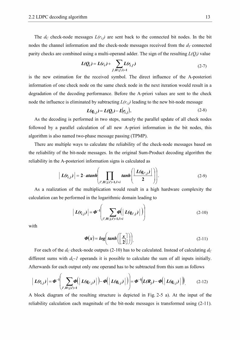
For each of the dC check-node outputs (2-10) has to be calculated. Instead of calculating dC
different sums with dC-1 operands it is possible to calculate the sum of all inputs initially.
Afterwards for each output only one operand has to be subtracted from this sum as follows
( ) ( ) ( )( ))L(qΦ)L(RΦ)L(qΦ)L(qΦΦ)L(r jij
ijHi'
jiji'ji ,
)',(,
,,, −=
−= −
=
− ∑ 1
1
1
. (2-12)
A block diagram of the resulting structure is depicted in Fig. 2-5 a). At the input of the
reliability calculation each magnitude of the bit-node messages is transformed using (2-11).
14 2 Introduction
Afterwards all the results are added with the subsequent subtraction of one value. Finally, the
reliability is calculated by applying Φ-1.
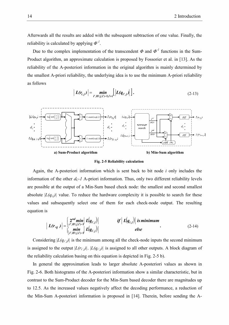
Due to the complex implementation of the transcendent Φ and Φ-1 functions in the Sum-
Product algorithm, an approximate calculation is proposed by Fossorier et al. in [13]. As the
reliability of the A-posteriori information in the original algorithm is mainly determined by
the smallest A-priori reliability, the underlying idea is to use the minimum A-priori reliability
as follows
[ ] .)L(qmin)L(r ji'iiijHi'
ji ,',)',(,
,≠=
=1 (2-13)
--
Cd Cd
( )( )xexpatanh2 ⋅
( )( )xexpatanh2 ⋅
2
tanhlogx
2
tanhlogx
1 0
1 0
CdCd
a) Sum-Product algorithm b) Min-Sum algorithm
Fig. 2-5 Reliability calculation
Again, the A-posteriori information which is sent back to bit node i only includes the
information of the other dC-1 A-priori information. Thus, only two different reliability levels
are possible at the output of a Min-Sum based check node: the smallest and second smallest
absolute |L(qi,j)| value. To reduce the hardware complexity it is possible to search for these
values and subsequently select one of them for each check-node output. The resulting
equation is
( ) ( )( ) .
elseqLmin
minimumisqLifqLmin
)L(rji
ijHi'
jijiijHi'
nd
ij
=
=
=
,')',(,
,,')',(,,
1
12
(2-14)
Considering |L(qi’,j)| is the minimum among all the check-node inputs the second minimum
is assigned to the output |L(ri’,j)|. |L(qi’,j)| is assigned to all other outputs. A block diagram of
the reliability calculation basing on this equation is depicted in Fig. 2-5 b).
In general the approximation leads to larger absolute A-posteriori values as shown in
Fig. 2-6. Both histograms of the A-posteriori information show a similar characteristic, but in
contrast to the Sum-Product decoder for the Min-Sum based decoder there are magnitudes up
to 12.5. As the increased values negatively affect the decoding performance, a reduction of
the Min-Sum A-posteriori information is proposed in [14]. Therein, before sending the A-
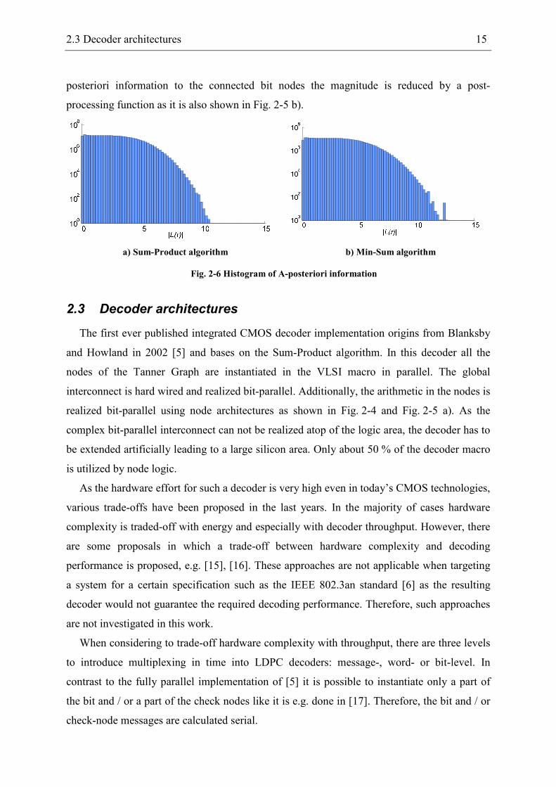
2.3 Decoder architectures 15
posteriori information to the connected bit nodes the magnitude is reduced by a post-
processing function as it is also shown in Fig. 2-5 b).
a) Sum-Product algorithm b) Min-Sum algorithm
Fig. 2-6 Histogram of A-posteriori information
2.3 Decoder architectures
The first ever published integrated CMOS decoder implementation origins from Blanksby
and Howland in 2002 [5] and bases on the Sum-Product algorithm. In this decoder all the
nodes of the Tanner Graph are instantiated in the VLSI macro in parallel. The global
interconnect is hard wired and realized bit-parallel. Additionally, the arithmetic in the nodes is
realized bit-parallel using node architectures as shown in Fig. 2-4 and Fig. 2-5 a). As the
complex bit-parallel interconnect can not be realized atop of the logic area, the decoder has to
be extended artificially leading to a large silicon area. Only about 50 % of the decoder macro
is utilized by node logic.
As the hardware effort for such a decoder is very high even in today’s CMOS technologies,
various trade-offs have been proposed in the last years. In the majority of cases hardware
complexity is traded-off with energy and especially with decoder throughput. However, there
are some proposals in which a trade-off between hardware complexity and decoding
performance is proposed, e.g. [15], [16]. These approaches are not applicable when targeting
a system for a certain specification such as the IEEE 802.3an standard [6] as the resulting
decoder would not guarantee the required decoding performance. Therefore, such approaches
are not investigated in this work.
When considering to trade-off hardware complexity with throughput, there are three levels
to introduce multiplexing in time into LDPC decoders: message-, word- or bit-level. In
contrast to the fully parallel implementation of [5] it is possible to instantiate only a part of
the bit and / or a part of the check nodes like it is e.g. done in [17]. Therefore, the bit and / or
check-node messages are calculated serial.
16 2 Introduction
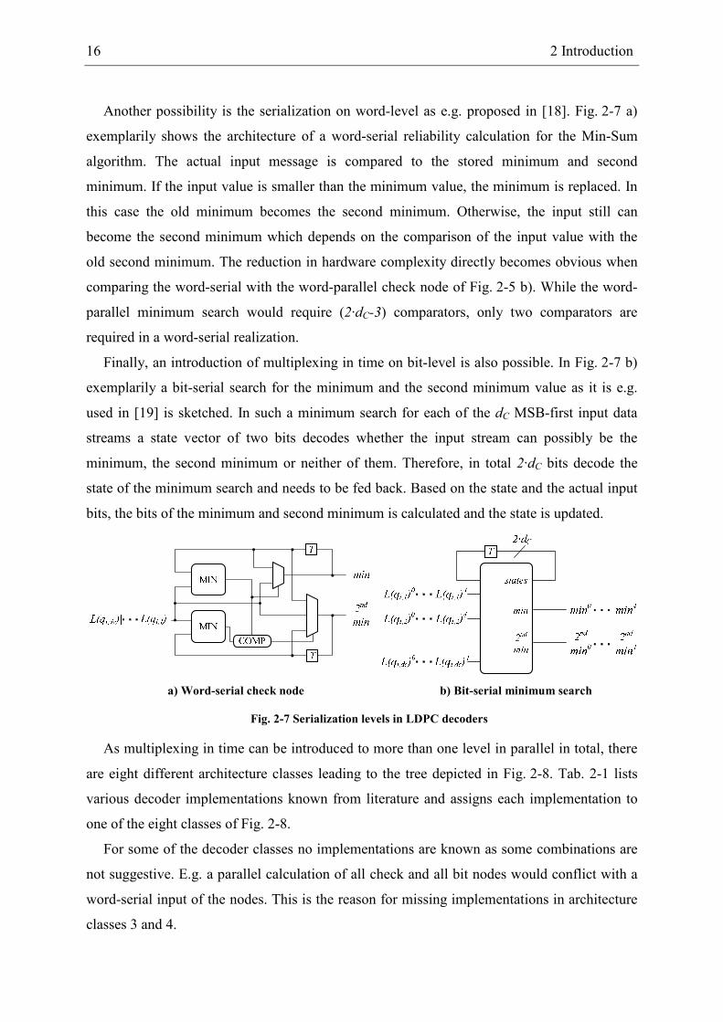
Another possibility is the serialization on word-level as e.g. proposed in [18]. Fig. 2-7 a)
exemplarily shows the architecture of a word-serial reliability calculation for the Min-Sum
algorithm. The actual input message is compared to the stored minimum and second
minimum. If the input value is smaller than the minimum value, the minimum is replaced. In
this case the old minimum becomes the second minimum. Otherwise, the input still can
become the second minimum which depends on the comparison of the input value with the
old second minimum. The reduction in hardware complexity directly becomes obvious when
comparing the word-serial with the word-parallel check node of Fig. 2-5 b). While the word-
parallel minimum search would require (2·dC-3) comparators, only two comparators are
required in a word-serial realization.
Finally, an introduction of multiplexing in time on bit-level is also possible. In Fig. 2-7 b)
exemplarily a bit-serial search for the minimum and the second minimum value as it is e.g.
used in [19] is sketched. In such a minimum search for each of the dC MSB-first input data
streams a state vector of two bits decodes whether the input stream can possibly be the
minimum, the second minimum or neither of them. Therefore, in total 2·dC bits decode the
state of the minimum search and needs to be fed back. Based on the state and the actual input
bits, the bits of the minimum and second minimum is calculated and the state is updated.
a) Word-serial check node b) Bit-serial minimum search
Fig. 2-7 Serialization levels in LDPC decoders
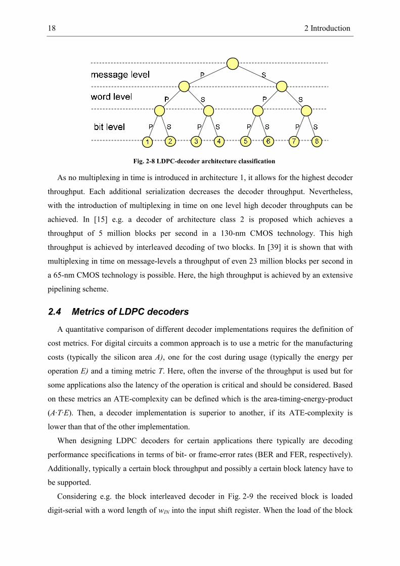
As multiplexing in time can be introduced to more than one level in parallel in total, there
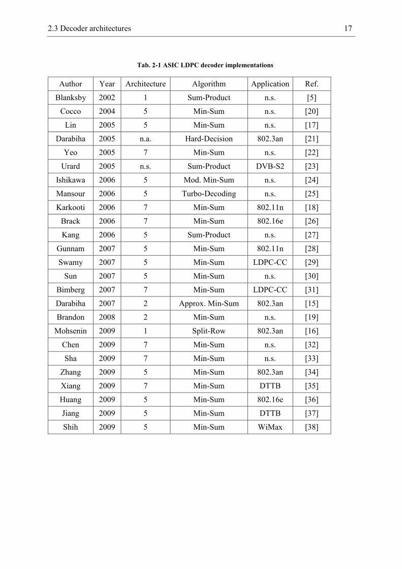
are eight different architecture classes leading to the tree depicted in Fig. 2-8. Tab. 2-1 lists
various decoder implementations known from literature and assigns each implementation to
one of the eight classes of Fig. 2-8.
For some of the decoder classes no implementations are known as some combinations are
not suggestive. E.g. a parallel calculation of all check and all bit nodes would conflict with a
word-serial input of the nodes. This is the reason for missing implementations in architecture
classes 3 and 4.
2.3 Decoder architectures 17
Tab. 2-1 ASIC LDPC decoder implementations
Author Year Architecture Algorithm Application Ref.
Blanksby 2002 1 Sum-Product n.s. [5]
Cocco 2004 5 Min-Sum n.s. [20]
Lin 2005 5 Min-Sum n.s. [17]
Darabiha 2005 n.a. Hard-Decision 802.3an [21]
Yeo 2005 7 Min-Sum n.s. [22]
Urard 2005 n.s. Sum-Product DVB-S2 [23]
Ishikawa 2006 5 Mod. Min-Sum n.s. [24]
Mansour 2006 5 Turbo-Decoding n.s. [25]
Karkooti 2006 7 Min-Sum 802.11n [18]
Brack 2006 7 Min-Sum 802.16e [26]
Kang 2006 5 Sum-Product n.s. [27]
Gunnam 2007 5 Min-Sum 802.11n [28]
Swamy 2007 5 Min-Sum LDPC-CC [29]
Sun 2007 5 Min-Sum n.s. [30]
Bimberg 2007 7 Min-Sum LDPC-CC [31]
Darabiha 2007 2 Approx. Min-Sum 802.3an [15]
Brandon 2008 2 Min-Sum n.s. [19]
Mohsenin 2009 1 Split-Row 802.3an [16]
Chen 2009 7 Min-Sum n.s. [32]
Sha 2009 7 Min-Sum n.s. [33]
Zhang 2009 5 Min-Sum 802.3an [34]
Xiang 2009 7 Min-Sum DTTB [35]
Huang 2009 5 Min-Sum 802.16e [36]
Jiang 2009 5 Min-Sum DTTB [37]
Shih 2009 5 Min-Sum WiMax [38]
18 2 Introduction
Fig. 2-8 LDPC-decoder architecture classification
As no multiplexing in time is introduced in architecture 1, it allows for the highest decoder
throughput. Each additional serialization decreases the decoder throughput. Nevertheless,
with the introduction of multiplexing in time on one level high decoder throughputs can be
achieved. In [15] e.g. a decoder of architecture class 2 is proposed which achieves a
throughput of 5 million blocks per second in a 130-nm CMOS technology. This high
throughput is achieved by interleaved decoding of two blocks. In [39] it is shown that with
multiplexing in time on message-levels a throughput of even 23 million blocks per second in
a 65-nm CMOS technology is possible. Here, the high throughput is achieved by an extensive
pipelining scheme.
2.4 Metrics of LDPC decoders
A quantitative comparison of different decoder implementations requires the definition of
cost metrics. For digital circuits a common approach is to use a metric for the manufacturing
costs (typically the silicon area A), one for the cost during usage (typically the energy per
operation E) and a timing metric T. Here, often the inverse of the throughput is used but for
some applications also the latency of the operation is critical and should be considered. Based
on these metrics an ATE-complexity can be defined which is the area-timing-energy-product
(A·T·E). Then, a decoder implementation is superior to another, if its ATE-complexity is
lower than that of the other implementation.
When designing LDPC decoders for certain applications there typically are decoding
performance specifications in terms of bit- or frame-error rates (BER and FER, respectively).
Additionally, typically a certain block throughput and possibly a certain block latency have to
be supported.
Considering e.g. the block interleaved decoder in Fig. 2-9 the received block is loaded
digit-serial with a word length of wIN into the input shift register. When the load of the block
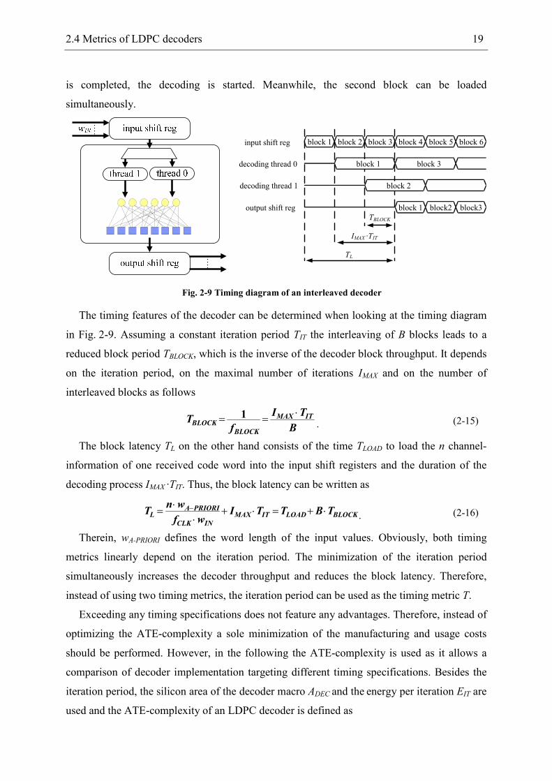
2.4 Metrics of LDPC decoders 19
is completed, the decoding is started. Meanwhile, the second block can be loaded
simultaneously.
block 1 block2 block3
block 4 block 5 block 6
block 1 block 3
output shift reg
block 1 block 2 block 3
block 2
decoding thread 0
input shift reg
TBLOCK
IMAX ·TIT
TL
decoding thread 1
Fig. 2-9 Timing diagram of an interleaved decoder
The timing features of the decoder can be determined when looking at the timing diagram
in Fig. 2-9. Assuming a constant iteration period TIT the interleaving of B blocks leads to a
reduced block period TBLOCK, which is the inverse of the decoder block throughput. It depends
on the iteration period, on the maximal number of iterations IMAX and on the number of
interleaved blocks as follows
B
TI
fT ITMAX
BLOCK
BLOCK
⋅== 1
. (2-15)
The block latency TL on the other hand consists of the time TLOAD to load the n channel-
information of one received code word into the input shift registers and the duration of the
decoding process IMAX ·TIT. Thus, the block latency can be written as
BLOCKLOADITMAX
INCLK
PRIORIAL TBTTI
wf
wnT ⋅+=⋅+
⋅⋅
= −. (2-16)
Therein, wA-PRIORI defines the word length of the input values. Obviously, both timing
metrics linearly depend on the iteration period. The minimization of the iteration period
simultaneously increases the decoder throughput and reduces the block latency. Therefore,
instead of using two timing metrics, the iteration period can be used as the timing metric T.
Exceeding any timing specifications does not feature any advantages. Therefore, instead of
optimizing the ATE-complexity a sole minimization of the manufacturing and usage costs
should be performed. However, in the following the ATE-complexity is used as it allows a
comparison of decoder implementation targeting different timing specifications. Besides the
iteration period, the silicon area of the decoder macro ADEC and the energy per iteration EIT are
used and the ATE-complexity of an LDPC decoder is defined as
20 2 Introduction
ITITDEC ETAcomplexityATE ⋅⋅=− . (2-17)
In the following, this metric will be used to quantitatively compare different design choices
throughout the design process and to compare different decoder implementations in a
benchmarking.
3 Generic ATE-cost models of LDPC decoders
The design of ATE-efficient LDPC decoders requires an optimization and, therefore, a
quantitative analysis on all design levels. Thus, accurate ATE-cost models are mandatory,
especially in early design phases as these allow for the highest optimization potential. For less
complex logic structures like e.g. finite-impulse-response filters the derivation of generic cost
models is more simple, as e.g. the circuit features are dominated by the logic leading to a
simple gate count. In contrast LDPC decoders are dominated by the exchange of the messages
between the two nodes and, therefore, for decoders of architecture classes 1 and 2 (Fig. 2-8)
by the complex interconnect.
As the impact of the interconnect varies significantly depending on whether it is realized
bit-serial or bit-parallel, two separate cost models for the two architecture classes 1 and 2 are
derived [40]. These models are primarily targeting a Min-Sum-based LDPC decoder.
However, it will be shown that they can be extended to support decoders which base on the
Sum-Product algorithm, as well.
3.1 Bit-parallel LDPC decoder
In the decoder loop at least one system delay is required which should be located at the
position leading to the smallest number of registers. A decoder loop for a Min-Sum-based
decoder and the equations to calculate the number of registers for the five depicted cross
sections is stated in Fig. 3-1.
-
1) wdmwdn CV ⋅⋅=⋅⋅
2) ( ) ( ) [ ]VC dldwdm +−⋅+⋅ 12
3) wdmwdn CV ⋅⋅=⋅⋅
4) ( ) ( )1++⋅+⋅⋅ VV dldwnwdn
5) ( ) ( )1++⋅⋅ VV dldwdn
Fig. 3-1 Bandwidth of message communication
Thereby, w defines the word length of the messages which are communicated between the
bit and the check nodes. As discussed in [41] the optimal position for the system delay can be
22 3 Generic ATE-cost models of LDPC decoders
observed at cross section two. At this point all the information is compressed to the two
minima, to the position of the minimum and to the sign signals. Therefore, in the following
the registers are assumed to be at this cross section and, thus, the area and energy impact can
be neglected.
3.1.1 Logic area
A lower bound of the decoder’s silicon area is the accumulated area of all required logic
gates. For a rough estimation the control logic of a bit-parallel decoder can be neglected.
Thus, the decoder logic mainly consists of the bit-parallel realization of the arithmetic in the n
bit- and m check-node instances.
One bit node mainly contains a multi-operand adder and the subsequent subtractors as
shown in Fig. 3-2. The multi-operand adder summarizes dV A-posteriori information and the
channel information leading to dV two-operand adders. Additionally, dV adders are required to
subtract the A-posteriori information from the resulting L(Qi) value.
Accounting for the required sign extension of the operands to the resulting word length of
( ) VBNEXT dldww +=_
(3-1)
bit the bit node includes
( ) ( )VVFAPBN dldwdN +⋅⋅= 2__
(3-2)
full adders (FA).
( ) 11 ++Vdld
--
Fig. 3-2 Data-path bit node
This adder scheme requires a two’s-complement representation of the A-posteriori
information. However, due to the separate sign and magnitude calculation in the check node
two conversions between the two number representations are required. The hardware effort of
the converters at the input of the bit node includes dV ·(w-1) XOR-gates to calculate the one’s
complement. The conversion to two’s complement is done using free carry inputs of the
3.1 Bit-parallel LDPC decoder 23
multi-operand adders. Each two’s-complement to sign-magnitude converter at the output of
the bit node consists of (w-1) XOR-gates and (w-1) half adders (HA) . With
XORHAXORFA AAAA ⋅≈+≈ 2
(3-3)
the logic area of the bit-parallel bit node can be roughly estimated to
( ) [ ] FAvvPBN AdldwdA ⋅⋅+−⋅⋅≈ 25153 .._ . (3-4)
As discussed in chapter 2.2, the Min-Sum check node is built up of a sign calculation, a
minimum search, logic to select either the absolute or the second minimum, and an optional
post-processing function. Thereby, the major contribution is due to the minimum search. The
search for the smallest and second smallest of the dC magnitudes is a sub problem of the
complete sorting of dC values. A lot of hardware-efficient sorters have been proposed in the
past, especially in the field of signal and image processing applications. One sorter
architecture, known for its minimal number of compare-and-swap (cs-) elements bases on the
odd-even merge algorithm [42]. Therein, subgroups of operands are sorted and afterwards
merged together.
For the given problem the merging of the subgroups can be simplified since only the two
smallest operands of each group are required. Exemplarily, an eight-operand sorter is
illustrated in Fig. 3-3 a) in which each subgroup only consists of two operands. After the
initial sorting of these operands, each merge operation requires three additional cs-elements
leading to a total number of
32 −⋅= CCN_P_CS dN
(3-5)
cs-elements.
One possible implementation of a cs-element would be the subtraction of the two operands
with a subsequent swap. Thereby, the sign of the difference indicates whether the two
operands have to be swapped. This can be realized by two multiplexer. The critical path of
such an element would begin at the LSB input of the subtractor, run through the whole adder
ripple path, and end at the outputs of the multiplexers. The output is not known until the sign
of the difference is calculated. Therefore, the concatenation of k cs-elements would result in a
critical path containing k adder ripple paths.
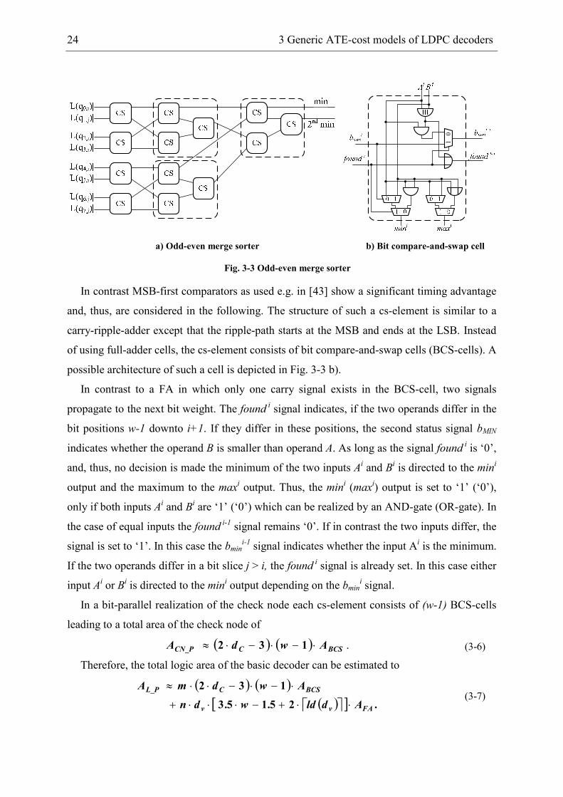
24 3 Generic ATE-cost models of LDPC decoders
1 0
a) Odd-even merge sorter b) Bit compare-and-swap cell
Fig. 3-3 Odd-even merge sorter
In contrast MSB-first comparators as used e.g. in [43] show a significant timing advantage
and, thus, are considered in the following. The structure of such a cs-element is similar to a
carry-ripple-adder except that the ripple-path starts at the MSB and ends at the LSB. Instead
of using full-adder cells, the cs-element consists of bit compare-and-swap cells (BCS-cells). A
possible architecture of such a cell is depicted in Fig. 3-3 b).
In contrast to a FA in which only one carry signal exists in the BCS-cell, two signals
propagate to the next bit weight. The found i signal indicates, if the two operands differ in the
bit positions w-1 downto i+1. If they differ in these positions, the second status signal bMIN
indicates whether the operand B is smaller than operand A. As long as the signal found i is ‘0’,
and, thus, no decision is made the minimum of the two inputs Ai and B
i is directed to the min
i
output and the maximum to the maxi output. Thus, the min
i (max
i) output is set to ‘1’ (‘0’),
only if both inputs Ai and B
i are ‘1’ (‘0’) which can be realized by an AND-gate (OR-gate). In
the case of equal inputs the found i-1 signal remains ‘0’. If in contrast the two inputs differ, the
signal is set to ‘1’. In this case the bmini-1 signal indicates whether the input A
i is the minimum.
If the two operands differ in a bit slice j > i, the found i signal is already set. In this case either
input Ai or B
i is directed to the min
i output depending on the bmin
i signal.
In a bit-parallel realization of the check node each cs-element consists of (w-1) BCS-cells
leading to a total area of the check node of
( ) ( ) .BCSCCN_P AwdA ⋅−⋅−⋅≈ 132
(3-6)
Therefore, the total logic area of the basic decoder can be estimated to
( ) ( )( ) [ ] .Adld.w.dn
AwdmA
FAvv
BCSCL_P
⋅⋅+−⋅⋅⋅+
⋅−⋅−⋅⋅≈
25153
132
(3-7)
3.1 Bit-parallel LDPC decoder 25
3.1.2 Routing area
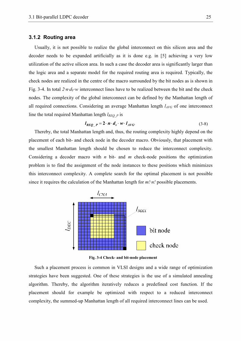
Usually, it is not possible to realize the global interconnect on this silicon area and the
decoder needs to be expanded artificially as it is done e.g. in [5] achieving a very low
utilization of the active silicon area. In such a case the decoder area is significantly larger than
the logic area and a separate model for the required routing area is required. Typically, the
check nodes are realized in the centre of the macro surrounded by the bit nodes as is shown in
Fig. 3-4. In total 2·n·dV·w interconnect lines have to be realized between the bit and the check
nodes. The complexity of the global interconnect can be defined by the Manhattan length of
all required connections. Considering an average Manhattan length lAVG of one interconnect
line the total required Manhattan length lREQ_P is
._ AVGvPREQ lwdnl ⋅⋅⋅⋅= 2
(3-8)
Thereby, the total Manhattan length and, thus, the routing complexity highly depend on the
placement of each bit- and check node in the decoder macro. Obviously, that placement with
the smallest Manhattan length should be chosen to reduce the interconnect complexity.
Considering a decoder macro with n bit- and m check-node positions the optimization
problem is to find the assignment of the node instances to these positions which minimizes
this interconnect complexity. A complete search for the optimal placement is not possible
since it requires the calculation of the Manhattan length for m!·n! possible placements.
l DEC
Fig. 3-4 Check- and bit-node placement
Such a placement process is common in VLSI designs and a wide range of optimization
strategies have been suggested. One of these strategies is the use of a simulated annealing
algorithm. Thereby, the algorithm iteratively reduces a predefined cost function. If the
placement should for example be optimized with respect to a reduced interconnect
complexity, the summed-up Manhattan length of all required interconnect lines can be used.
26 3 Generic ATE-cost models of LDPC decoders
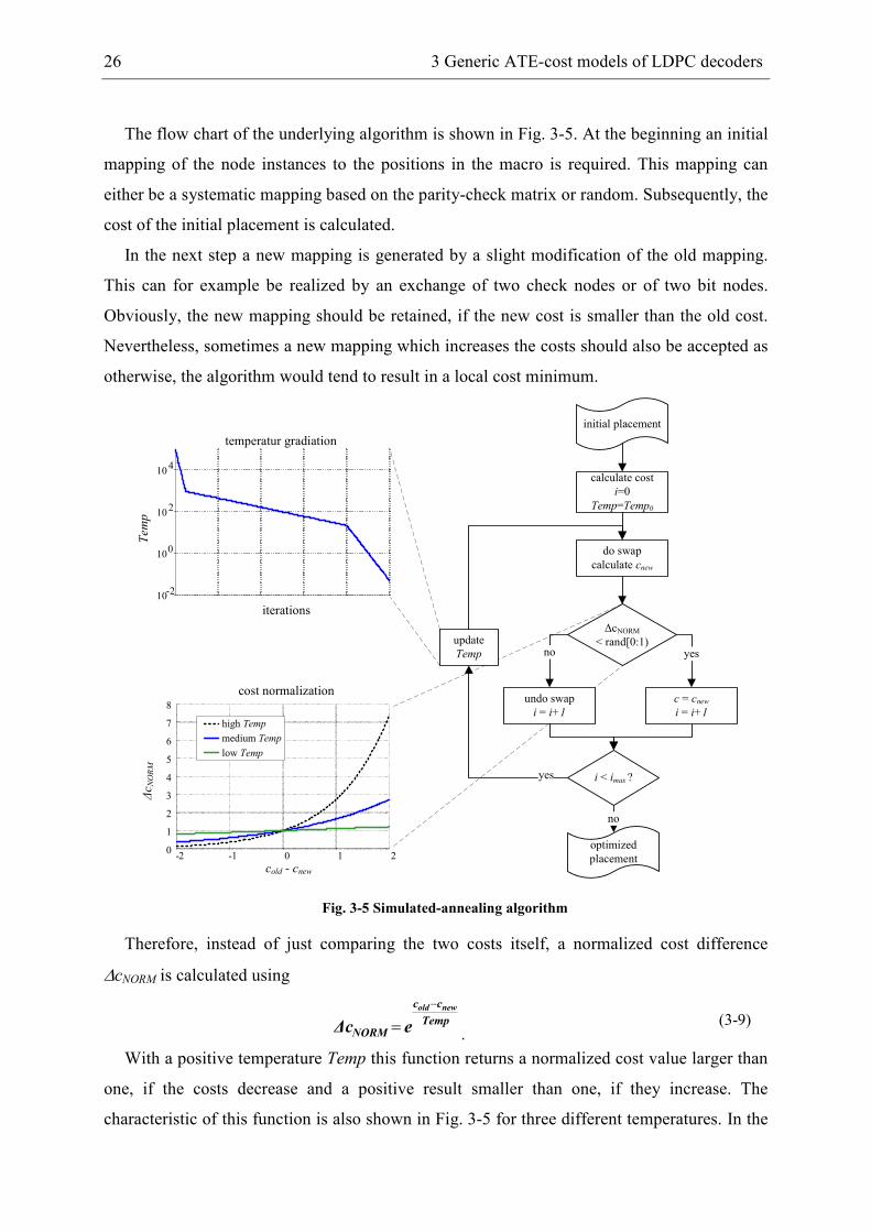
The flow chart of the underlying algorithm is shown in Fig. 3-5. At the beginning an initial
mapping of the node instances to the positions in the macro is required. This mapping can
either be a systematic mapping based on the parity-check matrix or random. Subsequently, the
cost of the initial placement is calculated.
In the next step a new mapping is generated by a slight modification of the old mapping.
This can for example be realized by an exchange of two check nodes or of two bit nodes.
Obviously, the new mapping should be retained, if the new cost is smaller than the old cost.
Nevertheless, sometimes a new mapping which increases the costs should also be accepted as
otherwise, the algorithm would tend to result in a local cost minimum.
initial placement
calculate cost
i=0
Temp=Temp0
do swap
calculate cnew
∆cNORM< rand[0:1)
no
undo swap
i = i+1
i < imax ?yes
no
yes
optimized
placement
c = cnewi = i+1
update
Temp
-2 -1 0 1 20
1
2
3
4
5
6
7
8
cold - cnew
high Temp
medium Temp
low Temp
cost normalization
10-2
100
102
104
Tem
p
iterations
temperatur gradiation
∆c N
ORM
Fig. 3-5 Simulated-annealing algorithm
Therefore, instead of just comparing the two costs itself, a normalized cost difference
∆cNORM is calculated using
Temp
cc
NORM
newold
e∆c
−
=.
(3-9)
With a positive temperature Temp this function returns a normalized cost value larger than
one, if the costs decrease and a positive result smaller than one, if they increase. The
characteristic of this function is also shown in Fig. 3-5 for three different temperatures. In the
3.1 Bit-parallel LDPC decoder 27
simulated annealing algorithm the result of this normalization is compared to a random
number between ‘0’ and ‘1’. If the result is larger than the random number, the modified
placement is kept and the costs are updated. Otherwise, the modification is undone. This
process is repeated until the defined maximum number of iterations is performed.
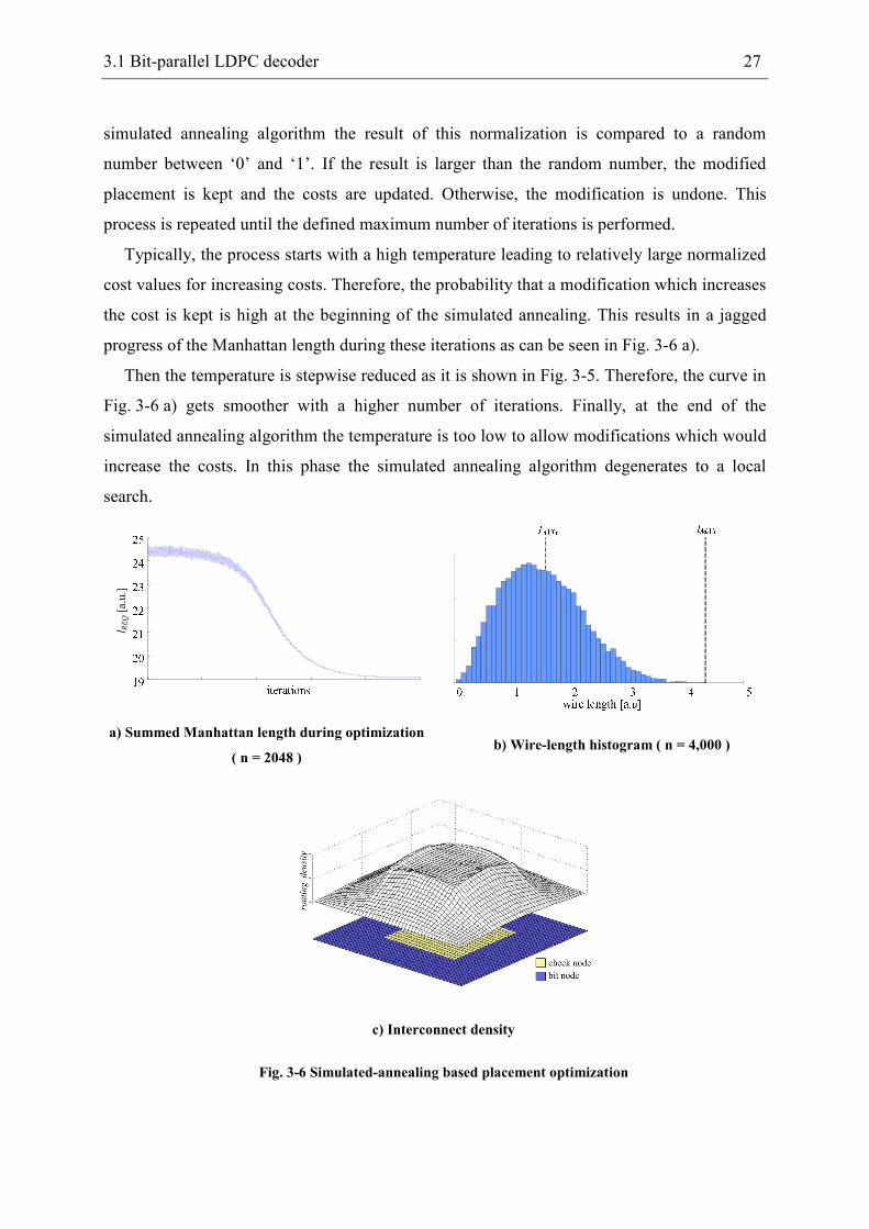
Typically, the process starts with a high temperature leading to relatively large normalized
cost values for increasing costs. Therefore, the probability that a modification which increases
the cost is kept is high at the beginning of the simulated annealing. This results in a jagged
progress of the Manhattan length during these iterations as can be seen in Fig. 3-6 a).
Then the temperature is stepwise reduced as it is shown in Fig. 3-5. Therefore, the curve in
Fig. 3-6 a) gets smoother with a higher number of iterations. Finally, at the end of the
simulated annealing algorithm the temperature is too low to allow modifications which would
increase the costs. In this phase the simulated annealing algorithm degenerates to a local
search.
l REQ[a.u.]
a) Summed Manhattan length during optimization
( n = 2048 ) b) Wire-length histogram ( n = 4,000 )
c) Interconnect density
Fig. 3-6 Simulated-annealing based placement optimization
28 3 Generic ATE-cost models of LDPC decoders
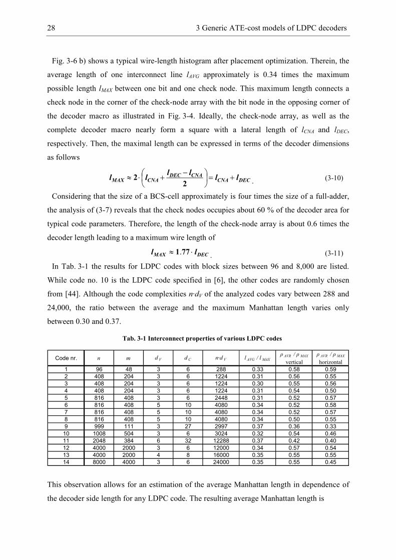
Fig. 3-6 b) shows a typical wire-length histogram after placement optimization. Therein, the
average length of one interconnect line lAVG approximately is 0.34 times the maximum
possible length lMAX between one bit and one check node. This maximum length connects a
check node in the corner of the check-node array with the bit node in the opposing corner of
the decoder macro as illustrated in Fig. 3-4. Ideally, the check-node array, as well as the
complete decoder macro nearly form a square with a lateral length of lCNA and lDEC,
respectively. Then, the maximal length can be expressed in terms of the decoder dimensions
as follows
DECCNACNADEC
CNAMAX llll
ll +=
−
+⋅≈2
2.
(3-10)
Considering that the size of a BCS-cell approximately is four times the size of a full-adder,
the analysis of (3-7) reveals that the check nodes occupies about 60 % of the decoder area for
typical code parameters. Therefore, the length of the check-node array is about 0.6 times the
decoder length leading to a maximum wire length of
DECMAX ll ⋅≈ 771.. (3-11)
In Tab. 3-1 the results for LDPC codes with block sizes between 96 and 8,000 are listed.
While code no. 10 is the LDPC code specified in [6], the other codes are randomly chosen
from [44]. Although the code complexities n·dV of the analyzed codes vary between 288 and
24,000, the ratio between the average and the maximum Manhattan length varies only
between 0.30 and 0.37.
Tab. 3-1 Interconnect properties of various LDPC codes
Code nr. n m d V d C n·d V l AVG / l MAX
ρ AVR / ρ MAX
vertical
ρ AVR / ρ MAX
horizontal
1 96 48 3 6 288 0.33 0.58 0.59
2 408 204 3 6 1224 0.31 0.56 0.55
3 408 204 3 6 1224 0.30 0.55 0.56
4 408 204 3 6 1224 0.31 0.54 0.50
5 816 408 3 6 2448 0.31 0.52 0.57
6 816 408 5 10 4080 0.34 0.52 0.58
7 816 408 5 10 4080 0.34 0.52 0.57
8 816 408 5 10 4080 0.34 0.50 0.55
9 999 111 3 27 2997 0.37 0.36 0.33
10 1008 504 3 6 3024 0.32 0.54 0.46
11 2048 384 6 32 12288 0.37 0.42 0.40
12 4000 2000 3 6 12000 0.34 0.57 0.54
13 4000 2000 4 8 16000 0.35 0.55 0.55
14 8000 4000 3 6 24000 0.35 0.55 0.45
This observation allows for an estimation of the average Manhattan length in dependence of
the decoder side length for any LDPC code. The resulting average Manhattan length is
3.1 Bit-parallel LDPC decoder 29
DECMAX lll ⋅≈⋅≈ 60350 ... (3-12)
Using (3-8) and (3-12) the total Manhattan length of the global interconnect of a bit-parallel
decoder can be estimated to
DECvPREQ lwdnl ⋅⋅⋅⋅≈ 21._ . (3-13)
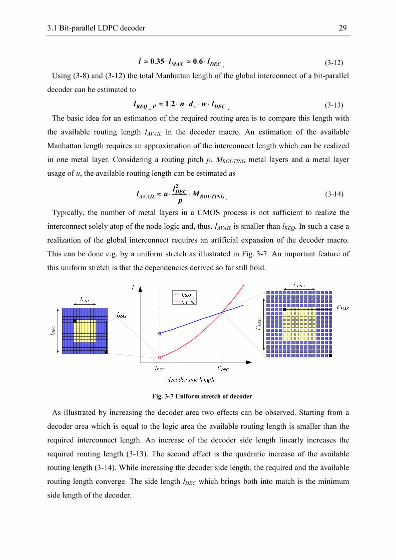
The basic idea for an estimation of the required routing area is to compare this length with
the available routing length lAVAIL in the decoder macro. An estimation of the available
Manhattan length requires an approximation of the interconnect length which can be realized
in one metal layer. Considering a routing pitch p, MROUTING metal layers and a metal layer
usage of u, the available routing length can be estimated as
ROUTINGDEC
AVAIL Mp
lul ⋅⋅≈
2
. (3-14)
Typically, the number of metal layers in a CMOS process is not sufficient to realize the
interconnect solely atop of the node logic and, thus, lAVAIL is smaller than lREQ. In such a case a
realization of the global interconnect requires an artificial expansion of the decoder macro.
This can be done e.g. by a uniform stretch as illustrated in Fig. 3-7. An important feature of
this uniform stretch is that the dependencies derived so far still hold.
l’DEC
l DEC
Fig. 3-7 Uniform stretch of decoder
As illustrated by increasing the decoder area two effects can be observed. Starting from a
decoder area which is equal to the logic area the available routing length is smaller than the
required interconnect length. An increase of the decoder side length linearly increases the
required routing length (3-13). The second effect is the quadratic increase of the available
routing length (3-14). While increasing the decoder side length, the required and the available
routing length converge. The side length lDEC which brings both into match is the minimum
side length of the decoder.
30 3 Generic ATE-cost models of LDPC decoders
Before calculating the decoder side length and the routing area a further improvement of the
estimation for the available Manhattan length is necessary. If the decoder area is increased
artificially, the utilization of the active silicon area is reduced. This is also true for the lower
metal layers which are used to realize the local interconnect. To minimize the required routing
area the lower metal layers should also be utilized for the global interconnect in these regions
between the nodes. The resulting available Manhattan length can therefore be approximated
using
( )[ ]M,llminMlp
ul L_PDECROUTINGL_PAVAIL ⋅−+⋅⋅≈ 0222
. (3-15)
The first term in (3-15) is the available routing length on the MROUTING layers atop of the
nodes. If the decoder area is larger than the logic area, the second term approximates the
available interconnect length in the regions between the node logic using M metal layers.
The decoder side length can now be estimated based on (3-13) and (3-15) leading to
( )[ ]MllMlp
lwdn LPDECROUTINGLPDECv ⋅−+⋅⋅=⋅⋅⋅⋅ 2225021 __..
. (3-16)
Therein an utilization factor of u = 0.5 is assumed. Even if an ideal routing algorithm
would exist, it would not be possible to use 100% of each metal layer. The reason is the
structure of the routing problem. The interconnect density for an optimized placement for the
(2048,1723) code [6] is depicted in Fig. 3-6 c). While a high interconnect density at the
boundary of the check-node array is observed, the density at the outer part of the macro is
low. A utilization factor can be derived by comparing the average ρAVG to the maximum
density ρMAX. The quotient of these two values for the different codes is given in Tab. 3-1, as
well. Although the quotient varies between 0.4 and 0.6 a utilization factor of u = 0.5 is
assumed in the following as a first-order model.
Based on (3-16) the decoder side length and, thus, the routing area can be derived which is
given by
2
22
22121
−⋅−
⋅
⋅⋅⋅+⋅
⋅⋅⋅≈=
M
MMlp
M
wdnp
M
wdnlA ROUTING
LVV
PDECPR ..__ . (3-17)
3.1.3 Iteration period
For bit-parallel decoder implementations the iteration period can be calculated by
summing-up the critical path along the decoder loop (Fig. 3-1). Basically, this loop consists of
four parts: the arithmetic in the bit node, the interconnect between the bit- and the check node,
the arithmetic in the check node, and the interconnect back to the bit node. To estimate the
3.1 Bit-parallel LDPC decoder 31
critical path the bit- and check-node pair with the longest interconnect length lMAX has to be
considered. For a rough approximation of the interconnect delay, the RC-delay of that
interconnect line is used which can be estimated as
22761690 PDECMAXPINT lCRlCRT __ ''.''. ⋅⋅⋅≈⋅⋅⋅≈
(3-18)
with R’ being the resistive and C’ the capacitive load per unit length. The critical path inside
the bit node (see Fig. 3-2) runs through
( ) 11 ++Vdld
(3-19)
adder and subtractor stages. Considering a carry ripple adder implementation of the multi-
operand adder inside the bit node and the extension of the word length the path can be
approximated by
( ) ( ) FAVPBN TwdldT ⋅++⋅≈ 12_ . (3-20)
The depth of the odd-even merge tree in the check node is
( ) 12 −⋅ Cdld
(3-21)
leading to a critical path of
( ) ( ) BCSCPCN TwdldT ⋅−+⋅≈ 22_ . (3-22)
With (3-18), (3-20), and (3-22) the iteration period can be written as
( ) ( ) ( ) ( ) 25232212 DECBCSCFAVPIT lCRTwdldTwdldT ⋅⋅⋅+⋅−+⋅+⋅++⋅≈ ''._ .
(3-23)
3.1.4 Energy per iteration
The dynamic power consumption highly depends on the switching activities of each
capacitive node inside the decoder. The AC power of the interconnect lines depends e.g. on
the mean switching activities of the quantized A-priori values L(qi,j) and A-posteriori values
L(ri,j). These in turn highly depend on the considered signal-to-noise ratio (SNR). Fig. 3-8
exemplarily shows the switching activities for each decoding iteration for the (2048,1723)
code [6] with w = 6. For a very low SNR of two dB the switching activity saturates to a
relatively high activity as the decoder does not converge. For higher SNR a high switching
activity is observed in the first decoding iterations and a lower activity when the decoder has
converged. Additionally, the average switching activities depend on the number of maximal
decoding iterations as more iterations lower the average switching activity.
However, typically a certain BER is specified which has to be guaranteed for a certain
application. Considering for example eight decoding iterations, it is possible to determine the
SNR for a given code to reach a BER of e.g. 10-5. In Fig. 3-8 b) the average switching
activities for the different LDPC codes of Tab. 3-1 for the individual SNR to reach a BER of
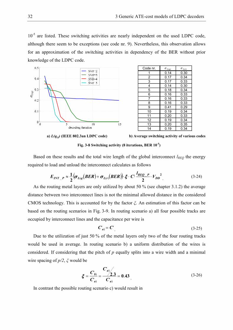
32 3 Generic ATE-cost models of LDPC decoders
10-5 are listed. These switching activities are nearly independent on the used LDPC code,
although there seem to be exceptions (see code nr. 9). Nevertheless, this observation allows
for an approximation of the switching activities in dependency of the BER without prior
knowledge of the LDPC code.
σL(q)
Code nr. σ L(q) σ L(r)
1 0.14 0.30
2 0.17 0.34
3 0.17 0.33
4 0.14 0.30
5 0.18 0.34
6 0.16 0.33
7 0.16 0.33
8 0.16 0.33
9 0.41 0.29
10 0.19 0.34
11 0.20 0.33
12 0.19 0.34
13 0.20 0.35
14 0.19 0.34
a) L(qi,j) (IEEE 802.3an LDPC code) b) Average switching activity of various codes
Fig. 3-8 Switching activity (8 iterations, BER 10-5)
Based on these results and the total wire length of the global interconnect lREQ the energy
required to load and unload the interconnect calculates as follows
( ) ( )( ) 2
22
1DD
PREQrLqLPINT V
lCBERBERE ⋅⋅⋅⋅+≈ _
)()(_ 'ξξξξσσσσσσσσ . (3-24)
As the routing metal layers are only utilized by about 50 % (see chapter 3.1.2) the average
distance between two interconnect lines is not the minimal allowed distance in the considered
CMOS technology. This is accounted for by the factor ξ. An estimation of this factor can be
based on the routing scenarios in Fig. 3-9. In routing scenario a) all four possible tracks are
occupied by interconnect lines and the capacitance per wire is
'' ) CC a =. (3-25)
Due to the utilization of just 50 % of the metal layers only two of the four routing tracks
would be used in average. In routing scenario b) a uniform distribution of the wires is
considered. If considering that the pitch of p equally splits into a wire width and a minimal
wire spacing of p/2, ξ would be
43032 .'.
'
'
'
)
)
)
) ===a
a
a
b
C
C
C
Cξξξξ .
(3-26)
In contrast the possible routing scenario c) would result in
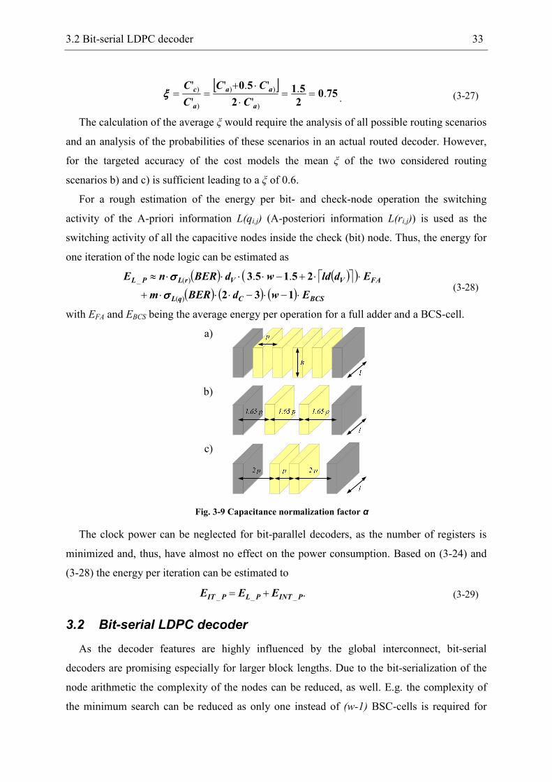
3.2 Bit-serial LDPC decoder 33
[ ]750
2
51
2
50..
'
'.'
'
'
)
))
)
) ==⋅
⋅+==
a
aa
a
c
C
CC
C
Cξξξξ . (3-27)
The calculation of the average ξ would require the analysis of all possible routing scenarios
and an analysis of the probabilities of these scenarios in an actual routed decoder. However,
for the targeted accuracy of the cost models the mean ξ of the two considered routing
scenarios b) and c) is sufficient leading to a ξ of 0.6.
For a rough estimation of the energy per bit- and check-node operation the switching
activity of the A-priori information L(qi,j) (A-posteriori information L(ri,j)) is used as the
switching activity of all the capacitive nodes inside the check (bit) node. Thus, the energy for
one iteration of the node logic can be estimated as
( ) ( ) ( )( ) ( ) ( ) BCSCqL
FAVVrLPL
EwdBERm
EdldwdBERnE
⋅−⋅−⋅⋅⋅+
⋅⋅+−⋅⋅⋅⋅≈
132
25153
)(
)(_ ..
σσσσ
σσσσ
(3-28)
with EFA and EBCS being the average energy per operation for a full adder and a BCS-cell.
a)
b)
c)
Fig. 3-9 Capacitance normalization factor α
The clock power can be neglected for bit-parallel decoders, as the number of registers is
minimized and, thus, have almost no effect on the power consumption. Based on (3-24) and
(3-28) the energy per iteration can be estimated to
.___ PINTPLPIT EEE +=
(3-29)
3.2 Bit-serial LDPC decoder
As the decoder features are highly influenced by the global interconnect, bit-serial
decoders are promising especially for larger block lengths. Due to the bit-serialization of the
node arithmetic the complexity of the nodes can be reduced, as well. E.g. the complexity of
the minimum search can be reduced as only one instead of (w-1) BSC-cells is required for
34 3 Generic ATE-cost models of LDPC decoders
each compare-and-swap element. However, as the cs-operation is processed in multiple clock
cycles the status signals found and bmin have to be stored in a register as shown in Fig. 3-10.
The two additional storage elements also need to be reset at the beginning of a new
comparison. Therefore, the area of the minimum search can be estimated as
( ) ( ).AAAdA MUXREGBCScCN_S_MIN ⋅+⋅+⋅−⋅≈ 2232
(3-30)
w-1
BCS BCS BCSBCS BCS BCS
resetmax
imini
Ai
Bi
bmini
found i
Fig. 3-10 Bit-parallel and bit-serial CS element
In contrast to the area model of the bit-parallel check node the area contribution of the
registers to store the two minima, the position of the minimum and the signs of the check-
node messages can not be neglected for a bit-serial check node. The area of these registers e.g.
approximately is
( ) ( ) ( ) REGCcCN_S_M_REG AdldwdA ⋅+−⋅+≈ 12 . (3-31)
Furthermore, additional control logic has to be included into the area model to prevent an
underestimation of the decoder’s logic area. Therefore, a more detailed look at the
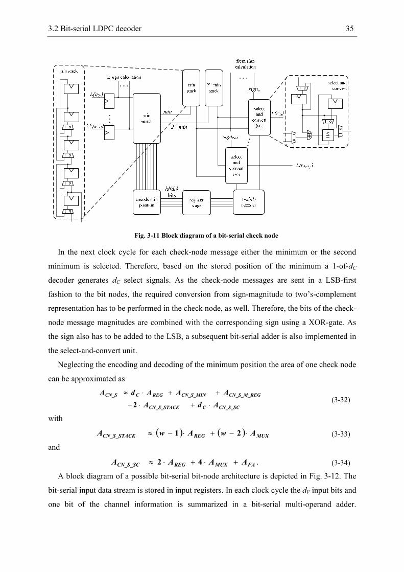
implementation of a bit-serial check node is required. A block diagram of a possible
architecture is depicted in Fig. 3-11.
The bit-serial input stream of the bit-node messages is stored in registers at the input of the
node. In the first clock cycle the signs of the bit-node messages are processed in the sign
calculation unit which is not depicted. The resulting bits are stored in the select-and-convert
units at the output of the check node. In the following clock cycles the minimum search is
performed. The underlying structure of the minimum search is equal to the one in Fig. 3-3 but
using the bit-serial cs-elements of Fig. 3-10. The bit-serial output of the minimum search is
stored in two stacks. After the LSBs of the bit-node messages have been processed, the
location of the minimal input can be determined based on the bmin signals of all the cs-
elements. To reduce the number of registers the position is encoded to a minimal number of
( ) Cdld bits.
3.2 Bit-serial LDPC decoder 35
Fig. 3-11 Block diagram of a bit-serial check node
In the next clock cycle for each check-node message either the minimum or the second
minimum is selected. Therefore, based on the stored position of the minimum a 1-of-dC
decoder generates dC select signals. As the check-node messages are sent in a LSB-first
fashion to the bit nodes, the required conversion from sign-magnitude to two’s-complement
representation has to be performed in the check node, as well. Therefore, the bits of the check-
node message magnitudes are combined with the corresponding sign using a XOR-gate. As
the sign also has to be added to the LSB, a subsequent bit-serial adder is also implemented in
the select-and-convert unit.
Neglecting the encoding and decoding of the minimum position the area of one check node
can be approximated as
CN_S_SCCCN_S_STACK
CN_S_M_REGCN_S_MINREGCCN_S
AdA
AAAdA
⋅+⋅+
++⋅≈
2 (3-32)
with
( ) ( ) MUXREGCN_S_STACK AwAwA ⋅−+⋅−≈ 21
(3-33)
and
.FAMUXREGCN_S_SC AAAA +⋅+⋅≈ 42
(3-34)
A block diagram of a possible bit-serial bit-node architecture is depicted in Fig. 3-12. The
bit-serial input data stream is stored in input registers. In each clock cycle the dV input bits and
one bit of the channel information is summarized in a bit-serial multi-operand adder.
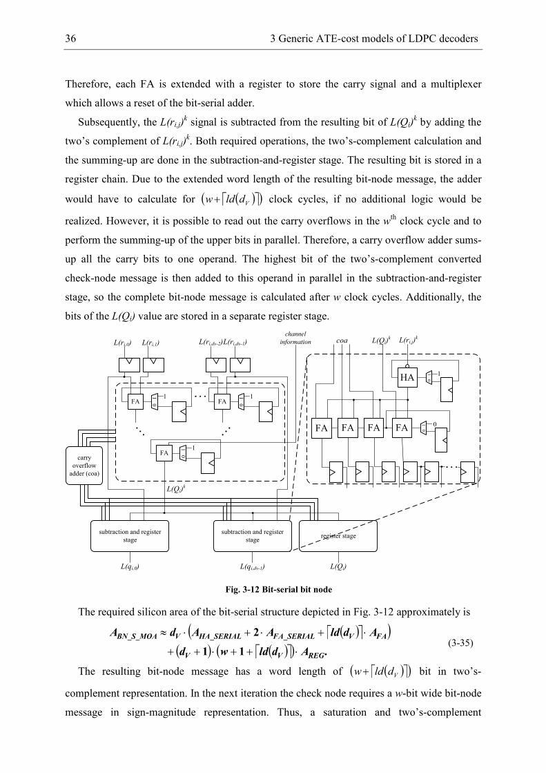
36 3 Generic ATE-cost models of LDPC decoders
Therefore, each FA is extended with a register to store the carry signal and a multiplexer
which allows a reset of the bit-serial adder.
Subsequently, the L(ri,j)k signal is subtracted from the resulting bit of L(Qi)
k by adding the
two’s complement of L(ri,j)k. Both required operations, the two’s-complement calculation and
the summing-up are done in the subtraction-and-register stage. The resulting bit is stored in a
register chain. Due to the extended word length of the resulting bit-node message, the adder
would have to calculate for ( ) ( )Vdldw+ clock cycles, if no additional logic would be
realized. However, it is possible to read out the carry overflows in the wth clock cycle and to
perform the summing-up of the upper bits in parallel. Therefore, a carry overflow adder sums-
up all the carry bits to one operand. The highest bit of the two’s-complement converted
check-node message is then added to this operand in parallel in the subtraction-and-register
stage, so the complete bit-node message is calculated after w clock cycles. Additionally, the
bits of the L(Qi) value are stored in a separate register stage.
L(ri,1)L(ri,0) L(ri,dv-2)L(ri,dv-1)
FA
1 0
1
FA
1 0
1FA
1 0
1
carry
overflow
adder (coa)
subtraction and register
stageregister stage
subtraction and register
stage
channel
information
HA
1 0
FA
1 0
1
0
L(ri,j)k
L(Qi)k
FA
coa
L(qi,0) L(qi,dv-1) L(Qi)
FAFA
L(Qi)k
Fig. 3-12 Bit-serial bit node
The required silicon area of the bit-serial structure depicted in Fig. 3-12 approximately is
( ) ( )( ) ( ) ( ) .Adldwd
AdldAAdA
REGVV
FAVFA_SERIALHA_SERIALVBN_S_MOA
⋅++⋅++
⋅+⋅+⋅≈
11
2
(3-35)
The resulting bit-node message has a word length of ( ) ( )Vdldw+ bit in two’s-
complement representation. In the next iteration the check node requires a w-bit wide bit-node
message in sign-magnitude representation. Thus, a saturation and two’s-complement
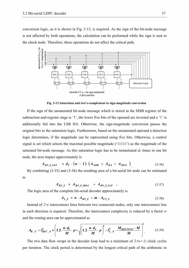
3.2 Bit-serial LDPC decoder 37
conversion logic, as it is shown in Fig. 3-13, is required. As the sign of the bit-node message
is not affected by both operations, the calculation can be performed while the sign is sent to
the check node. Therefore, these operations do not affect the critical path.
Fig. 3-13 Saturation and two’s-complement to sign-magnitude conversion
If the sign of the unsaturated bit-node message which is stored in the MSB register of the
subtraction-and-register stage is ‘1’, the lower five bits of the operand are inverted and a ‘1’ is
additionally fed into the LSB HA. Otherwise, the sign-magnitude conversion passes the
original bits to the saturation logic. Furthermore, based on the unsaturated operand a detection
logic determines, if the magnitude can be represented using five bits. Otherwise, a control
signal is set which selects the maximal possible magnitude (‘11111’) as the magnitude of the
saturated bit-node message. As this saturation logic has to be instantiated dV times in one bit
node, the area impact approximately is
( ) ( )MUXHAXORVBN_S_SAT AAAwdA ++⋅−⋅≈ 1. (3-36)
By combining (3-35) and (3-36) the resulting area of a bit-serial bit node can be estimated
to
.AAA BN_S_SATBN_S_MOABN_S +≈ (3-37)
The logic area of the complete bit-serial decoder approximately is
CN_SBN_SL_S AmAnA ⋅+⋅≈. (3-38)
Instead of 2·w interconnect lines between two connected nodes, only one interconnect line
in each direction is required. Therefore, the interconnect complexity is reduced by a factor w
and the routing area can be approximated as
2
22
22121
−⋅−
⋅
⋅⋅+⋅
⋅⋅≈=
M
MMlp
M
dnp
M
dnlA ROUTING
SLVV
SDECSR ___ ...
(3-39)
The two data flow swaps in the decoder loop lead to a minimum of 2·(w+1) clock cycles
per iteration. The clock period is determined by the longest critical path of the arithmetic in
38 3 Generic ATE-cost models of LDPC decoders
the nodes and the wire delay. In contrast to the nodes in the bit-parallel decoder, the critical
path is reduced due to the missing ripple path and is mainly determined by the depth of the
arithmetic. The critical path of the minimum search can be approximated as
( ) ( ) BCScCN_S TdldT ⋅−⋅≈ 12. (3-40)
The critical path of the bit-serial bit node runs through the multi-operand adder, the FA
which realizes the subtraction of L(ri,j), and the FAs required for the upper bits in the last
clock cycle of the bit-node calculation. Thus, the critical path approximately is
( ) ( ) [ ] FAvvSBN TdlddldT ⋅+++≈ 11_ . (3-41)
The iteration period of a bit-serial decoder can be roughly estimated as
( ) ( )SINTSBNSCNSIT TTTmaxwT ____ ,,⋅+⋅≈ 12
(3-42)
with TINT_S calculated using (3-18) with the maximum interconnect length lMAX for the bit-
serial decoder.
The arithmetic operations which have to be calculated in a bit-serial decoder do not differ
to a bit-parallel realization. The only difference in the calculation is that the operations are
carried out sequentially. Therefore, the energy of the logic in a bit-serial decoder can roughly
be estimated based on (3-28), as well. The average energy to load and unload the interconnect
per iteration can be estimated using (3-24). However, the switching activities of the
interconnect does not depend on the relation of one bit in consecutive iterations but on the
relation of subsequent bits in one L(qi,j) or L(ri,j) value. Nevertheless, the same switching
activity as for the bit-parallel decoder is assumed in the following.
One major difference in the energy of the bit-serial decoder is the higher clock power as a
significantly higher number of registers is required in the bit-serial decoder. The total number
of registers consists of the swap registers, the registers to hold the carry signal in the multi-
operand adder and the registers to hold the found- and bmin- signals in the minimum search.
The total number of registers approximately is
( ) ( ) .___ 44444 344444 214444 34444 21nodebitnodecheck −−
⋅+⋅+⋅⋅+−⋅⋅+⋅⋅≈ BNEXTVVCREGSDEC wdndnwmdmN 12123 (3-43)
The required energy of each clock cycle to load the input capacitance of all the registers in
the decoder approximately is
2
DDINREGREGSDECSCYCCLK VCNE ⋅⋅≈ _____ (3-44)
with CREG_IN being the accumulated input capacitance of all clock inputs of the registers.
Considering that one decoding iteration requires (2·w+2) clock cycles the corresponding
clock energy approximately is
3.3 Quantitative analysis of decoder architectures 39
( ) .____2
22 DDINREGREGSDECSCLK VCNwE ⋅⋅⋅+⋅≈
(3-45)
Thus, the total energy per iteration is
SCLKSINTSLSIT EEEE ____ ++=. (3-46)
3.3 Quantitative analysis of decoder architectures
The derived models (see also [45]) allow for an estimation of decoder features based on the
features of basic digital components like e.g. FAs and on technology parameters like the
routing pitch. For an estimation of the actual costs the features of logic gates, interconnect
lines, and registers have to be introduced into these models. In the following a quantitative
analysis of the cost models is done considering a physically optimized full-custom design
style. Therefore, the absolute cost metrics have to be regarded as lower bounds.
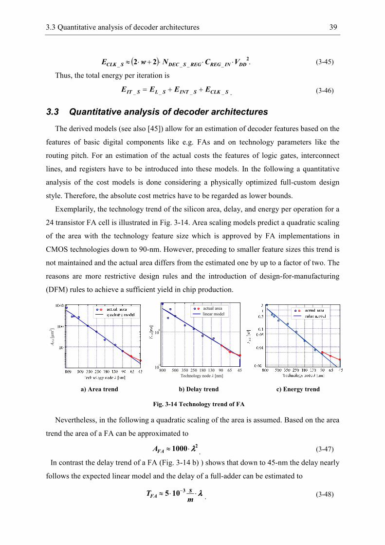
Exemplarily, the technology trend of the silicon area, delay, and energy per operation for a
24 transistor FA cell is illustrated in Fig. 3-14. Area scaling models predict a quadratic scaling
of the area with the technology feature size which is approved by FA implementations in
CMOS technologies down to 90-nm. However, preceding to smaller feature sizes this trend is
not maintained and the actual area differs from the estimated one by up to a factor of two. The
reasons are more restrictive design rules and the introduction of design-for-manufacturing
(DFM) rules to achieve a sufficient yield in chip production.
AFA[µm2]
45659013018025035050080010
-1
100
Technology node λ [nm]
actual area
linear model
a) Area trend b) Delay trend c) Energy trend
Fig. 3-14 Technology trend of FA
Nevertheless, in the following a quadratic scaling of the area is assumed. Based on the area
trend the area of a FA can be approximated to
21000 λλλλ⋅≈FAA.
(3-47)
In contrast the delay trend of a FA (Fig. 3-14 b) ) shows that down to 45-nm the delay nearly
follows the expected linear model and the delay of a full-adder can be estimated to
λλλλ⋅⋅≈ −
m
sTFA3
105.
(3-48)
40 3 Generic ATE-cost models of LDPC decoders
The reason for the continuity of the linear decreasing delay even for deep-submicron
technologies is the introduction of constant-voltage scaling for technologies smaller than
90-nm. In the technology generations down to 90-nm the supply voltage has been decreased
with the technology feature size leading to scaling of the energy with λ-3 as it can be seen in
Fig. 3-14 c). However, the constant voltage scaling results in an energy scaling with only λ-1.
To cope with this trend the energy per full-adder is estimated in dependence of the supply
voltage and the technology feature size to
2
235
mV
nJVE DDFA λλλλ⋅⋅≈.
(3-49)
The features of the other basic components which are required for the estimation of the
ATE-costs like the BCS-cells have been derived in a similar way and are listed in Tab. 3-2.
Tab. 3-2 ATE features of building blocks
FA BCS SCAN
REG MUX HA XOR
Silicon area [m2] 1,000·λ
2 4,000·λ
2 2,000·λ
2 500 λ
2 800·λ
2 500·λ
2
Delay [s] 5·10-3·λ 6·10
-3·λ 3·10
-3·λ
Energy per operation [nJ / mV2] 35·VDD
2·λ 190·VDD
2·λ
Additionally, the features of interconnect lines have to be modeled, as well. E.g. the
capacitive load per unit length, which in a first-order model is independent of the technology
feature size [46], can be determined to about C’ = 0.16 fF/µm. In contrast to the capacitive load
the resistive load highly depends on the technology feature size [46]. For a rough estimation
the resistive load can be approximated to scale with λ-2. Considering the miller-effect on the
capacitive load for worst-case timing the delay of an interconnect line with the length l can be
approximated to
slTINT ⋅⋅⋅≈−
2
2
181020
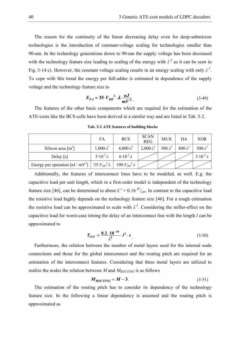
λ.
. (3-50)
Furthermore, the relation between the number of metal layers used for the internal node
connections and those for the global interconnect and the routing pitch are required for an
estimation of the interconnect features. Considering that three metal layers are utilized to
realize the nodes the relation between M and MROUTING is as follows
.3−= MMROUTING
(3-51)
The estimation of the routing pitch has to consider its dependency of the technology
feature size. In the following a linear dependency is assumed and the routing pitch is
approximated as
3.3 Quantitative analysis of decoder architectures 41
.λλλλ⋅= 2p
(3-52)
Finally, the capacitance of the clock input of the considered registers has to be
approximated for estimating the clock power of the bit-serial decoder. The input capacitance
of a static master-slave flip-flop including local clock wires can be determined by circuit
simulations and can be approximated to
λλλλ⋅≈m
nFC INREG 45_ . (3-53)
3.3.1 Bit-parallel decoder
The introduction of the implementation-style-dependent features into the decoder cost-
models allows for a quantitative analysis of the decoder features. E.g. based on (3-7) and on
the silicon area of the basic components taken from Tab. 3-2 the total logic area of a bit-
parallel decoder implementation can be estimated. Furthermore, introducing the considered
routing pitch of 2·λ into (3-17) yields in an approximation of the routing area. In Fig. 3-15 a)
the routing and logic area are outlined for an exemplary LDPC code and technology
parameter set. While the logic area scales linearly with the code block length, the routing area
scales quadratically. The resulting silicon area can then be estimated as the maximum of the
routing and the logic area. For small block lengths the interconnect between the nodes can be
realized atop of the logic area leading to a logic dominated decoder. In contrast for higher
block lengths the decoder area is determined by the area which is required to route the
complex interconnect. Based on (3-7) and (3-17) the boundary between logic and routing
dominated decoder can be derived. Approximately no artificial area extension is required, if
w
Mdn ROUTINGv
2
500 ⋅<⋅
(3-54)
leading to a logic dominated decoder. Therefore, the code complexity n·dV determines
whether a decoder is logic or routing dominated.
Obviously, the code complexity range for which no area extension is required gets smaller
the smaller the number of routing layers is. Fig. 3-15 b) quantitatively illustrates this
behavior. For MROUTING = ∞ the decoder area would be the logic area. By restricting the
number of routing layers to a large number of eight, only code complexities n·dV of less than
about 6,000 would result in a logic dominated decoder. A further limitation to six and four
metal layers would reduce the range to 3,500 and 1,500, respectively.
The iteration period of the bit-parallel decoder is the sum of the critical paths of the bit and
check node and twice the propagation delay of the longest interconnect line (see (3-23) ).
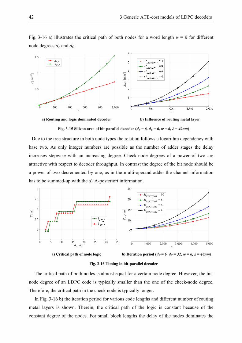
42 3 Generic ATE-cost models of LDPC decoders
Fig. 3-16 a) illustrates the critical path of both nodes for a word length w = 6 for different
node degrees dV and dC.
AL_P
AR_P
0 200 400 600 800 1,000
0.5
1
1.5
n
A[mm2]
ADEC [mm2]
a) Routing and logic dominated decoder b) Influence of routing metal layer
Fig. 3-15 Silicon area of bit-parallel decoder (dV = 6, dC = 6, w = 6, λ = 40nm)
Due to the tree structure in both node types the relation follows a logarithm dependency with
base two. As only integer numbers are possible as the number of adder stages the delay
increases stepwise with an increasing degree. Check-node degrees of a power of two are
attractive with respect to decoder throughput. In contrast the degree of the bit node should be
a power of two decremented by one, as in the multi-operand adder the channel information
has to be summed-up with the dV A-posteriori information.
T[ns]
0 1,000 2,000 3,000 4,000 5,000
5
10
15
20
25
n
MROUTING
= 10
MROUTING
= 8
MROUTING
= 6
MROUTING
= 4
a) Critical path of node logic b) Iteration period (dV = 6, dC = 32, w = 6, λ = 40nm)
Fig. 3-16 Timing in bit-parallel decoder
The critical path of both nodes is almost equal for a certain node degree. However, the bit-
node degree of an LDPC code is typically smaller than the one of the check-node degree.
Therefore, the critical path in the check node is typically longer.
In Fig. 3-16 b) the iteration period for various code lengths and different number of routing
metal layers is shown. Therein, the critical path of the logic is constant because of the
constant degree of the nodes. For small block lengths the delay of the nodes dominates the
3.3 Quantitative analysis of decoder architectures 43
iteration period of the bit-parallel decoder. However, for larger block length the impact of the
interconnect delay on the iteration period is significant. E.g. for a block length of about 2,800
and a usage of four routing metal layers the delay due to the interconnect equals the
propagation delay of the nodes for this kind of decoders.
E [nJ]
EIT_P [nJ]
a) Energy break-down (MROUTING = 8) b) Influence of number of routing layers
Fig. 3-17 Energy per iteration of bit-parallel decoder (dV = 6, dC = 32, w = 6, λ = 40nm)
The energy per iteration for a BER of 10-5 and a maximum number of decoding iterations
of eight is depicted in Fig. 3-17. The energy per iteration is separated into the logic and the
interconnect part in Fig. 3-17 a). For larger block lengths the energy to load and unload the
interconnect highly dominates the energy per iteration of the decoder. Thereby, up to 80 % of
the energy is due to the interconnect for a block length of 2,000.
Furthermore, the energy per iteration scales quadratically with the block length. As
illustrated in Fig. 3-17 b): the lower the number of metal layers is, the steeper is this increase.
3.3.2 Bit-serial decoder
The routing area of the bit-serial decoder is significantly smaller than the one of the bit-
parallel decoder. Again, the comparison of the logic area (3-38) and the routing area (3-39)
reveals an upper limit of the code complexity which still leads to a logic dominated decoder.
This code complexity approximately is
( ) .2
1501700 ROUTINGV Mwdn ⋅⋅+=⋅
(3-55)
As the absolute value of the right hand side of the equation is significantly higher than in
(3-54), only for higher code complexities the bit-serial decoder results in a routing dominated
decoder. Considering e.g. a message word length of six bit and four metal routing layers, only
LDPC codes with a code complexity larger than 40,000 lead to a routing dominated decoder.
For bit-parallel decoders the boundary lies at about 1,300.
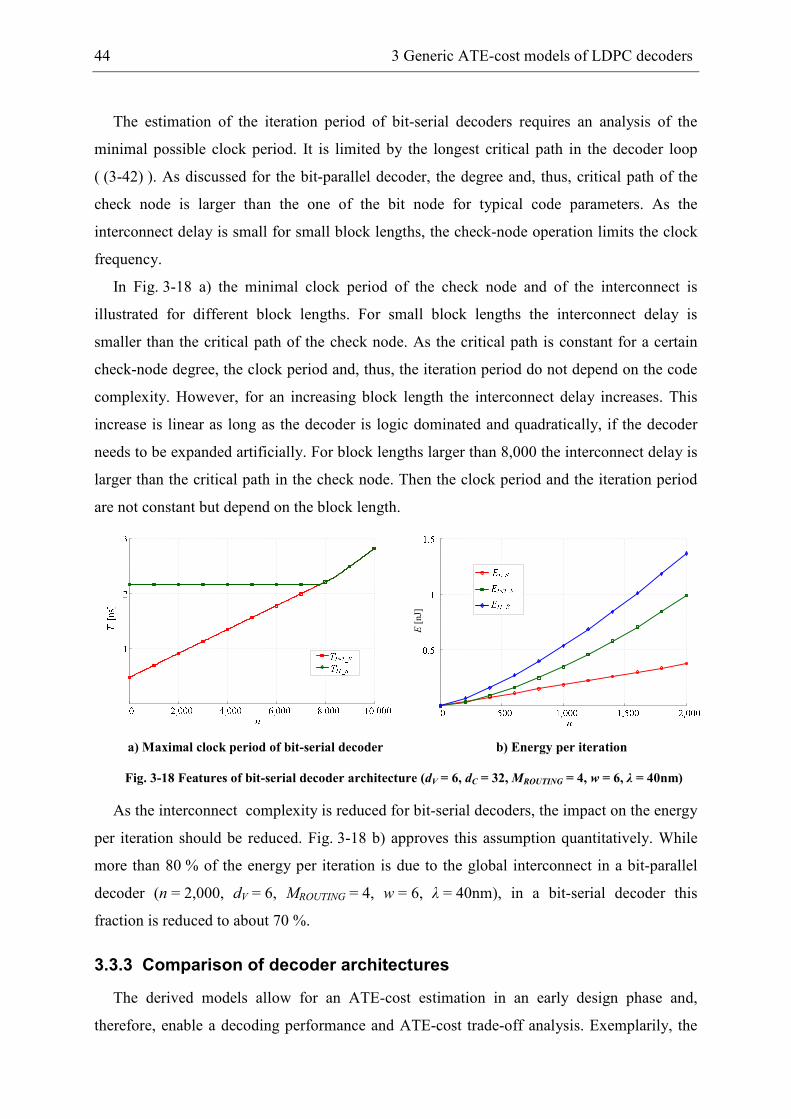
44 3 Generic ATE-cost models of LDPC decoders
The estimation of the iteration period of bit-serial decoders requires an analysis of the
minimal possible clock period. It is limited by the longest critical path in the decoder loop
( (3-42) ). As discussed for the bit-parallel decoder, the degree and, thus, critical path of the
check node is larger than the one of the bit node for typical code parameters. As the
interconnect delay is small for small block lengths, the check-node operation limits the clock
frequency.
In Fig. 3-18 a) the minimal clock period of the check node and of the interconnect is
illustrated for different block lengths. For small block lengths the interconnect delay is
smaller than the critical path of the check node. As the critical path is constant for a certain
check-node degree, the clock period and, thus, the iteration period do not depend on the code
complexity. However, for an increasing block length the interconnect delay increases. This
increase is linear as long as the decoder is logic dominated and quadratically, if the decoder
needs to be expanded artificially. For block lengths larger than 8,000 the interconnect delay is
larger than the critical path in the check node. Then the clock period and the iteration period
are not constant but depend on the block length.
E [nJ]
a) Maximal clock period of bit-serial decoder b) Energy per iteration
Fig. 3-18 Features of bit-serial decoder architecture (dV = 6, dC = 32, MROUTING = 4, w = 6, λ = 40nm)
As the interconnect complexity is reduced for bit-serial decoders, the impact on the energy
per iteration should be reduced. Fig. 3-18 b) approves this assumption quantitatively. While
more than 80 % of the energy per iteration is due to the global interconnect in a bit-parallel
decoder (n = 2,000, dV = 6, MROUTING = 4, w = 6, λ = 40nm), in a bit-serial decoder this
fraction is reduced to about 70 %.
3.3.3 Comparison of decoder architectures
The derived models allow for an ATE-cost estimation in an early design phase and,
therefore, enable a decoding performance and ATE-cost trade-off analysis. Exemplarily, the
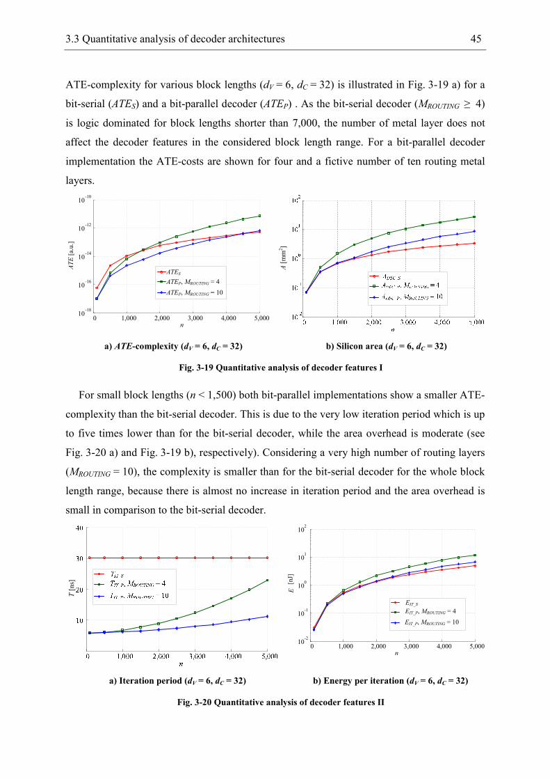
3.3 Quantitative analysis of decoder architectures 45
ATE-complexity for various block lengths (dV = 6, dC = 32) is illustrated in Fig. 3-19 a) for a
bit-serial (ATES) and a bit-parallel decoder (ATEP) . As the bit-serial decoder (MROUTING ≥ 4)
is logic dominated for block lengths shorter than 7,000, the number of metal layer does not
affect the decoder features in the considered block length range. For a bit-parallel decoder
implementation the ATE-costs are shown for four and a fictive number of ten routing metal
layers.
0 1,000 2,000 3,000 4,000 5,00010
-18
10-16
10-14
10-12
10-10
n
ATE [a.u.]
ATES
ATEP, MROUTING = 4
ATEP, MROUTING = 10
A[mm2]
a) ATE-complexity (dV = 6, dC = 32) b) Silicon area (dV = 6, dC = 32)
Fig. 3-19 Quantitative analysis of decoder features I
For small block lengths (n < 1,500) both bit-parallel implementations show a smaller ATE-
complexity than the bit-serial decoder. This is due to the very low iteration period which is up
to five times lower than for the bit-serial decoder, while the area overhead is moderate (see
Fig. 3-20 a) and Fig. 3-19 b), respectively). Considering a very high number of routing layers
(MROUTING = 10), the complexity is smaller than for the bit-serial decoder for the whole block
length range, because there is almost no increase in iteration period and the area overhead is
small in comparison to the bit-serial decoder.
T[ns]
0 1,000 2,000 3,000 4,000 5,00010
-2
10-1
100
101
102
n
E [nJ]
EIT_S
EIT_P, MROUTING = 4
EIT_P, MROUTING = 10
a) Iteration period (dV = 6, dC = 32) b) Energy per iteration (dV = 6, dC = 32)
Fig. 3-20 Quantitative analysis of decoder features II
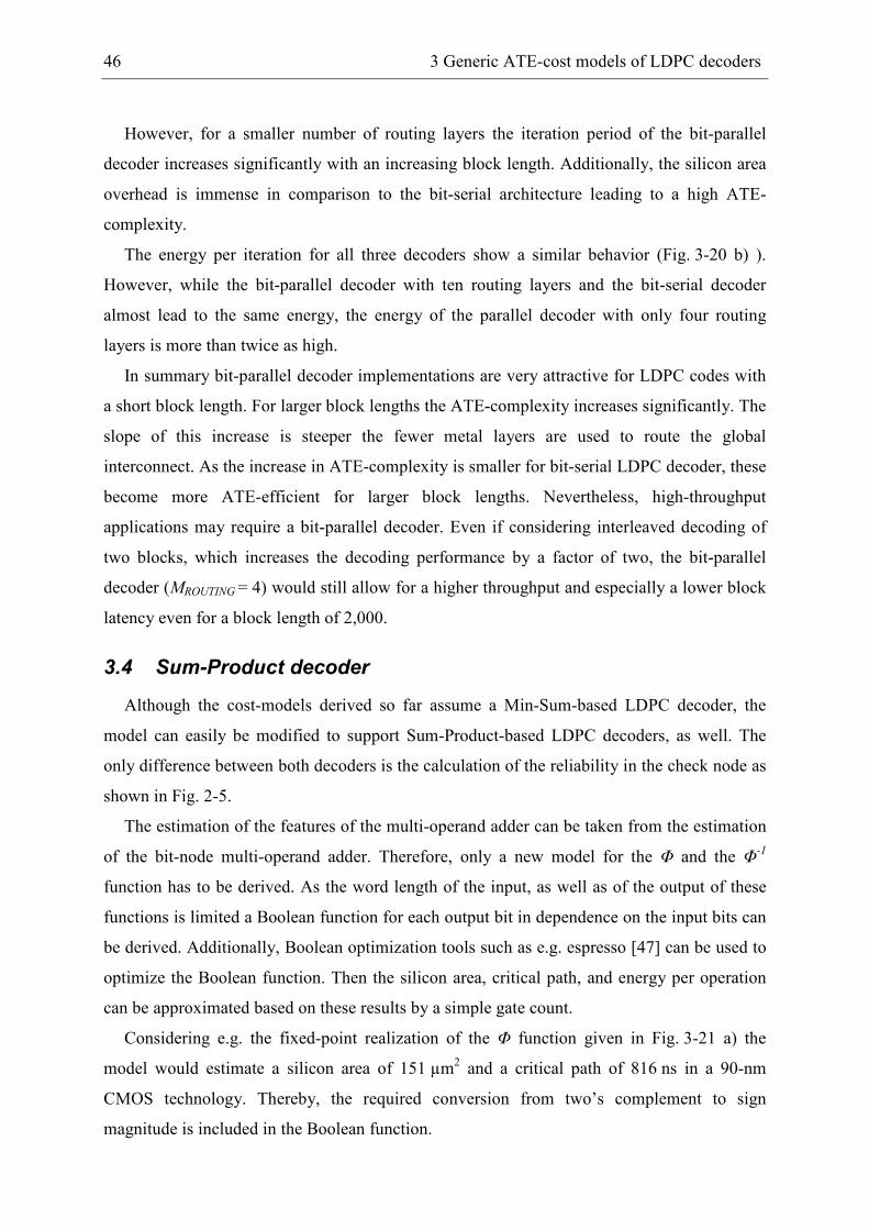
46 3 Generic ATE-cost models of LDPC decoders
However, for a smaller number of routing layers the iteration period of the bit-parallel
decoder increases significantly with an increasing block length. Additionally, the silicon area
overhead is immense in comparison to the bit-serial architecture leading to a high ATE-
complexity.
The energy per iteration for all three decoders show a similar behavior (Fig. 3-20 b) ).
However, while the bit-parallel decoder with ten routing layers and the bit-serial decoder
almost lead to the same energy, the energy of the parallel decoder with only four routing
layers is more than twice as high.
In summary bit-parallel decoder implementations are very attractive for LDPC codes with
a short block length. For larger block lengths the ATE-complexity increases significantly. The
slope of this increase is steeper the fewer metal layers are used to route the global
interconnect. As the increase in ATE-complexity is smaller for bit-serial LDPC decoder, these
become more ATE-efficient for larger block lengths. Nevertheless, high-throughput
applications may require a bit-parallel decoder. Even if considering interleaved decoding of
two blocks, which increases the decoding performance by a factor of two, the bit-parallel
decoder (MROUTING = 4) would still allow for a higher throughput and especially a lower block
latency even for a block length of 2,000.
3.4 Sum-Product decoder
Although the cost-models derived so far assume a Min-Sum-based LDPC decoder, the
model can easily be modified to support Sum-Product-based LDPC decoders, as well. The
only difference between both decoders is the calculation of the reliability in the check node as
shown in Fig. 2-5.
The estimation of the features of the multi-operand adder can be taken from the estimation
of the bit-node multi-operand adder. Therefore, only a new model for the Φ and the Φ-1
function has to be derived. As the word length of the input, as well as of the output of these
functions is limited a Boolean function for each output bit in dependence on the input bits can
be derived. Additionally, Boolean optimization tools such as e.g. espresso [47] can be used to
optimize the Boolean function. Then the silicon area, critical path, and energy per operation
can be approximated based on these results by a simple gate count.
Considering e.g. the fixed-point realization of the Φ function given in Fig. 3-21 a) the
model would estimate a silicon area of 151 µm2 and a critical path of 816 ns in a 90-nm
CMOS technology. Thereby, the required conversion from two’s complement to sign
magnitude is included in the Boolean function.
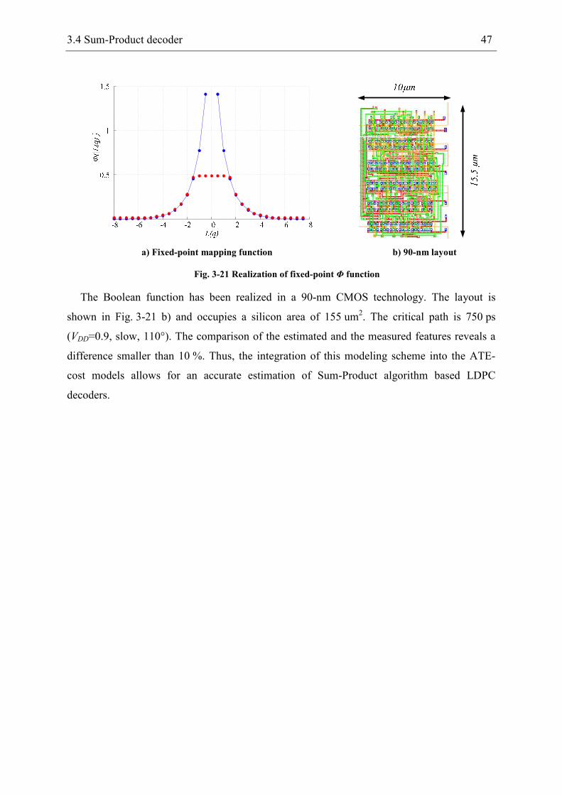
3.4 Sum-Product decoder 47
a) Fixed-point mapping function b) 90-nm layout
Fig. 3-21 Realization of fixed-point Φ function
The Boolean function has been realized in a 90-nm CMOS technology. The layout is
shown in Fig. 3-21 b) and occupies a silicon area of 155 um2. The critical path is 750 ps
(VDD=0.9, slow, 110°). The comparison of the estimated and the measured features reveals a
difference smaller than 10 %. Thus, the integration of this modeling scheme into the ATE-
cost models allows for an accurate estimation of Sum-Product algorithm based LDPC
decoders.

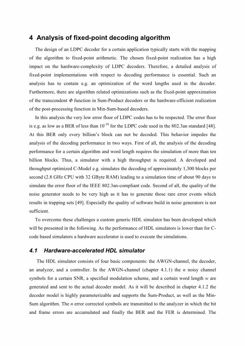
4 Analysis of fixed-point decoding algorithm
The design of an LDPC decoder for a certain application typically starts with the mapping
of the algorithm to fixed-point arithmetic. The chosen fixed-point realization has a high
impact on the hardware-complexity of LDPC decoders. Therefore, a detailed analysis of
fixed-point implementations with respect to decoding performance is essential. Such an
analysis has to contain e.g. an optimization of the word lengths used in the decoder.
Furthermore, there are algorithm related optimizations such as the fixed-point approximation
of the transcendent Φ function in Sum-Product decoders or the hardware-efficient realization
of the post-processing function in Min-Sum-based decoders.
In this analysis the very low error floor of LDPC codes has to be respected. The error floor
is e.g. as low as a BER of less than 10-10 for the LDPC code used in the 802.3an standard [48].
At this BER only every billion’s block can not be decoded. This behavior impedes the
analysis of the decoding performance in two ways. First of all, the analysis of the decoding
performance for a certain algorithm and word length requires the simulation of more than ten
billion blocks. Thus, a simulator with a high throughput is required. A developed and
throughput optimized C-Model e.g. simulates the decoding of approximately 1,300 blocks per
second (2.8 GHz CPU with 32 GByte RAM) leading to a simulation time of about 90 days to
simulate the error floor of the IEEE 802.3an-compliant code. Second of all, the quality of the
noise generator needs to be very high as it has to generate those rare error events which
results in trapping sets [49]. Especially the quality of software build in noise generators is not
sufficient.
To overcome these challenges a custom generic HDL simulator has been developed which
will be presented in the following. As the performance of HDL simulators is lower than for C-
code based simulators a hardware accelerator is used to execute the simulations.
4.1 Hardware-accelerated HDL simulator
The HDL simulator consists of four basic components: the AWGN-channel, the decoder,
an analyzer, and a controller. In the AWGN-channel (chapter 4.1.1) the n noisy channel
symbols for a certain SNR, a specified modulation scheme, and a certain word length w are
generated and sent to the actual decoder model. As it will be described in chapter 4.1.2 the
decoder model is highly parameterizable and supports the Sum-Product, as well as the Min-
Sum algorithm. The n error corrected symbols are transmitted to the analyzer in which the bit
and frame errors are accumulated and finally the BER and the FER is determined. The
50 4 Analysis of fixed-point decoding algorithm
simulator is controlled by a state-machine which synchronizes the AWGN-channel, the
decoder, and the analyzer.
4.1.1 AWGN Channel
The AWGN channel generates blocks of n noisy symbols. These are generated by adding
white Gaussian noise of a certain SNR to a code word. As the quality of the white Gaussian
noise can highly impact the analysis results, an accurate replication of the normal distribution
is crucial. Good hardware noise generators allow for a replication of the Gauss function in a
range of up to 8·σ [50]. Typically, the generation of a normal-distributed variable bases on a
transformation of a unified random variable into a normal-distributed variable. A possible
transformations is the Box-Muller method [51]. Due to its good properties with respect to
hardware realization the Box-Muller method is e.g. used in an FPGA-based hardware
generator in [50] which has been the basis of the implemented generator.
The algorithm converts two uniformly distributed random numbers in the range [0,1) u1
and u2 into two independent normally distributed variables n1, n2 ~ N(0,1) with a mean value
µ = 0 and a variance σ 2 = 1.
The basic ideas of the transformation become obvious when looking at the characteristics
of the two dimensional histogram of two normal-distributed random numbers n1 and n2. As
the distribution is rotational-symmetric, the probability for an angle ϕ on any circle of a radius
r is constant. Therefore, the normalized angle
⋅
⋅=⋅
⋅=
1
22
2
1
2
1
n
narctanu
ππππϕϕϕϕ
ππππ (4-1)
is uniformly distributed on [0,1).
Additionally, the square of the radius of this two-dimensional distribution follows a Chi-
squared distribution as the negative logarithm of a uniform-distributed variable does [51]
leading to
( ) .22
2
2
112 rnnulog =+=⋅−
(4-2)
Eq. (4-1) and (4-2) contain a transformation instruction to convert two uniformly
distributed variable u1 and u2 into two standard normal-distributed variables n1 and n2. As n1
and n2 can be written as
( )ϕϕϕϕcosrn ⋅=1 and ( ),ϕϕϕϕsinrn ⋅=2
(4-3)
it directly follows
( ) ( )ϕϕϕϕππππ ⋅⋅⋅⋅−= 22 11 cosulogn
(4-4)
and
4.1 Hardware-accelerated HDL simulator 51
( ) ( )ϕϕϕϕππππ ⋅⋅⋅⋅−= 22 12 sinulogn.
(4-5)
A block diagram of the modeled random noise generator is shown in Fig. 4-1. At the
beginning two uniform-distributed numbers u1 and u2 are generated. To assure highly accurate
normal-distributed noise samples the uniform-distributed noise samples have to be of high
quality, as well. Tausworthe random number generators which base on linear feedback shift
registers allow for a hardware-efficient realization of such a random number generator.
However, a too simple recursion would result in a low noise quality. In contrast combined
generators yield in a better stochastic characteristic and a higher sequence length.
Tausworthe
generator
n1 n2
u1 u2
h1 h2r
x0(SNR)0u2
a0
a1
-/++/-
-/+
a11
-/++/-
-/+
register stages
21
21
h1 h2
1121
− 1121
−
-/++/-
-/+
egr sqrt ⋅=
( ) ( )
( ) ( )22
21
21
21
ug
SNRh
ug
SNRh
sqrt
sqrt
⋅⋅⋅=
⋅⋅⋅=
πσ
πσ
cos
sin
( )12 ue log⋅−=
Fig. 4-1 Box-Muller-based converter
The implemented Tausworthe generator is taken from [52]. It consists of a combination of
three linear feedback shift registers which are based on the following primitive polynomials
.)(
)(
)(
1
1
1
3283
2292
13311
−−=
−−=
−−=
zzzP
zzzP
zzzP
(4-6)
The combination results in a linear feedback shift register with a maximum length of
288 ≈ 10
25.
Subsequently, the Box-Muller algorithm is performed to transform the uniform-distributed
variables u1 and u2 into normal-distributed variables n1 and n2 based on (4-4) and (4-5). The
52 4 Analysis of fixed-point decoding algorithm
calculation can be separated into a radius and an angle calculation. The angle calculation is a
transformation of polar into Cartesian coordinates on an unit circle. The radius r is calculated
in two steps. First of all, a variable e is calculated which is the negative logarithm of u1 and
which has a Chi-squared distribution. In a second step the radius r is derived by calculating
the square root of e. All operations can be efficiently realized using the Cordic-algorithm.
Then the originally proposed Box-Muller algorithm [51] should be modified. The Cordic-
based calculation of the sine / cosine and of the square root requires a subsequent
multiplication with an inverse gain factor. Instead of realizing the multipliers at the output of
the corresponding blocks it is possible to use an initial value
( ) ( )cossin/gg
SNRSNRxsqrt
11 ⋅⋅=σσσσ (4.7)
in the Cordic-based calculation of the sine and cosine as shown in Fig. 4-1. This factor also
includes the conversion from a N(0,1) normal-distributed random variable into a N(0,σ2)
distributed variable which is done by multiplying with the standard deviation σ
( )SNRnn ii σσσσ⋅='. (4.8)
To support a wide range of applications the noise generator is highly parameterizable.
Therefore, the word length of the uniform-distributed variables wu1 and wu2, of internal signals
and of the normal-distributed variables wn1 and wn2 can be adapted.
Exemplarily, a required range of the normal distribution of ±5·σ and a binary phase shift
keying modulation is considered. The maximum possible noise sample is determined by the
minimal possible value of u1. Based on (4-4) or (4-5) the minimal value can be determined to
3.7·10-6 which results in 19 fractional bits of u1. To avoid quantization effects a word length
wu1 = 20 is chosen. The output word length of the considered Tausworthe generators is 32
bits, leading to a word length of wu2 = 12. To account for the BPSK modulation scheme the
standard deviation for a certain SNR is given as [53]
( ) 10102
1SNR
SNR−
=σ.
(4.9)
For a SNR range of three to six dB the corresponding standard deviation would vary
between 0.5 und 0.35. Therefore, the scaling yields in a compression of the bell curve.
To evaluate the quality of the generated noise the distribution of the generated noisy
symbols are compared to the ideal normal distribution given as
−=2
2
1exp
2
1)(
σπσ
xxf
. (4.10)
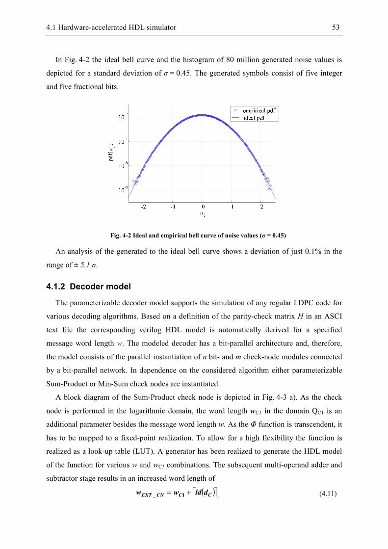
4.1 Hardware-accelerated HDL simulator 53
In Fig. 4-2 the ideal bell curve and the histogram of 80 million generated noise values is
depicted for a standard deviation of σ = 0.45. The generated symbols consist of five integer
and five fractional bits.
Fig. 4-2 Ideal and empirical bell curve of noise values (σ = 0.45)
An analysis of the generated to the ideal bell curve shows a deviation of just 0.1% in the
range of ± 5.1 σ.
4.1.2 Decoder model
The parameterizable decoder model supports the simulation of any regular LDPC code for
various decoding algorithms. Based on a definition of the parity-check matrix H in an ASCI
text file the corresponding verilog HDL model is automatically derived for a specified
message word length w. The modeled decoder has a bit-parallel architecture and, therefore,
the model consists of the parallel instantiation of n bit- and m check-node modules connected
by a bit-parallel network. In dependence on the considered algorithm either parameterizable
Sum-Product or Min-Sum check nodes are instantiated.
A block diagram of the Sum-Product check node is depicted in Fig. 4-3 a). As the check
node is performed in the logarithmic domain, the word length wC1 in the domain QC1 is an
additional parameter besides the message word length w. As the Φ function is transcendent, it
has to be mapped to a fixed-point realization. To allow for a high flexibility the function is
realized as a look-up table (LUT). A generator has been realized to generate the HDL model
of the function for various w and wC1 combinations. The subsequent multi-operand adder and
subtractor stage results in an increased word length of
( ) CCCNEXT dldww += 1_ . (4.11)
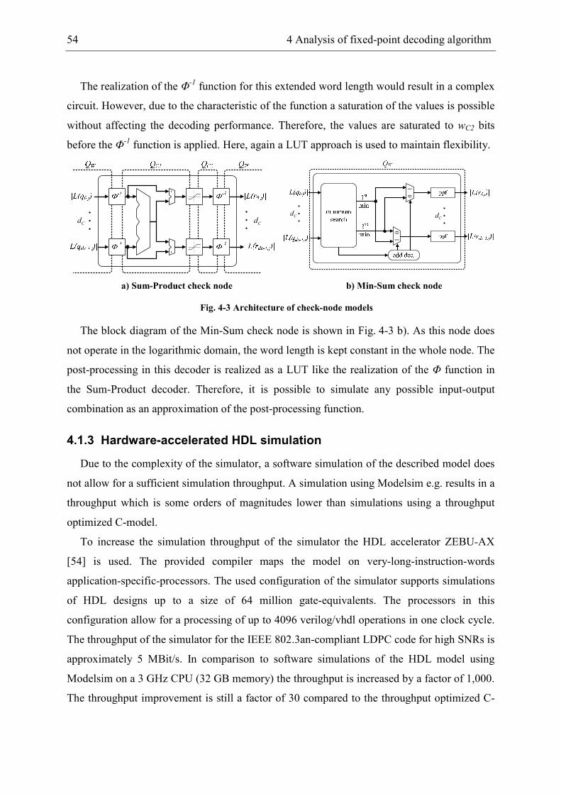
54 4 Analysis of fixed-point decoding algorithm
The realization of the Φ-1 function for this extended word length would result in a complex
circuit. However, due to the characteristic of the function a saturation of the values is possible
without affecting the decoding performance. Therefore, the values are saturated to wC2 bits
before the Φ-1 function is applied. Here, again a LUT approach is used to maintain flexibility.
Cd Cd
--
0 1
1 0
CdCd
a) Sum-Product check node b) Min-Sum check node
Fig. 4-3 Architecture of check-node models
The block diagram of the Min-Sum check node is shown in Fig. 4-3 b). As this node does
not operate in the logarithmic domain, the word length is kept constant in the whole node. The
post-processing in this decoder is realized as a LUT like the realization of the Φ function in
the Sum-Product decoder. Therefore, it is possible to simulate any possible input-output
combination as an approximation of the post-processing function.
4.1.3 Hardware-accelerated HDL simulation
Due to the complexity of the simulator, a software simulation of the described model does
not allow for a sufficient simulation throughput. A simulation using Modelsim e.g. results in a
throughput which is some orders of magnitudes lower than simulations using a throughput
optimized C-model.
To increase the simulation throughput of the simulator the HDL accelerator ZEBU-AX
[54] is used. The provided compiler maps the model on very-long-instruction-words
application-specific-processors. The used configuration of the simulator supports simulations
of HDL designs up to a size of 64 million gate-equivalents. The processors in this
configuration allow for a processing of up to 4096 verilog/vhdl operations in one clock cycle.
The throughput of the simulator for the IEEE 802.3an-compliant LDPC code for high SNRs is
approximately 5 MBit/s. In comparison to software simulations of the HDL model using
Modelsim on a 3 GHz CPU (32 GB memory) the throughput is increased by a factor of 1,000.
The throughput improvement is still a factor of 30 compared to the throughput optimized C-
4.2 Decoding performance analysis of fixed-point decoders 55
model. Additionally, in contrast to software build in noise generators the quality of the noise
generator is high enabling the analysis of even very low error floor.
4.2 Decoding performance analysis of fixed-point decoders
The described hardware simulator has been used to analyze the decoding performance of
the IEEE 802.3an-compliant LDPC code for the Sum-Product and the Min-Sum decoding
algorithm for a wide range of decoder-parameter sets.
4.2.1 Fixed-point effects on decoding performance
The used word length of the channel information L(ci) and of the messages L(qi,j) and L(ri,j)
communicated between the two node types highly affects the decoding performance. The
achievable performance varies in particular in comparison to floating-point implementations
of the decoding algorithm. The derivation of a required word length can be separated into the
determination of the integer and fractional bits. Thereby, a sufficient number of integer bits
are required to allow for a representation of the channel information in the whole probability
range. In Fig. 4-4 the probability distribution of the channel information L(ci) for various SNR
is depicted which are initialized using (2-6). Additionally, the saturation boundaries for up to
six integer bits are drawn. Only six integer bits allow for a correct representation of nearly all
possible channel symbols.
BER
Fig. 4-4 Quantization of L(ci) and impact on Sum-Product decoding performance (10 iterations)
Considering e.g. three integer and three fractional bits, a range between [-4,3.875] can be
represented using a two’s-complement representation. Thus, about 80 % of the channel
symbols would be saturated for an SNR of three dB. The decoding performance of such a
decoder is low as it can be seen in the BER chart of Fig. 4-4. The reason is the saturation of
channel symbols with a high reliability level leading to a reduction of the reliability level for
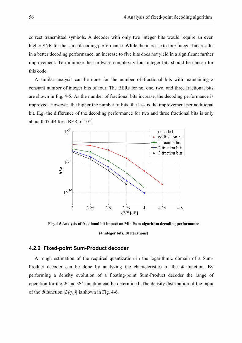
56 4 Analysis of fixed-point decoding algorithm
correct transmitted symbols. A decoder with only two integer bits would require an even
higher SNR for the same decoding performance. While the increase to four integer bits results
in a better decoding performance, an increase to five bits does not yield in a significant further
improvement. To minimize the hardware complexity four integer bits should be chosen for
this code.
A similar analysis can be done for the number of fractional bits with maintaining a
constant number of integer bits of four. The BERs for no, one, two, and three fractional bits
are shown in Fig. 4-5. As the number of fractional bits increase, the decoding performance is
improved. However, the higher the number of bits, the less is the improvement per additional
bit. E.g. the difference of the decoding performance for two and three fractional bits is only
about 0.07 dB for a BER of 10-9.
Fig. 4-5 Analysis of fractional bit impact on Min-Sum algorithm decoding performance
(4 integer bits, 10 iterations)
4.2.2 Fixed-point Sum-Product decoder
A rough estimation of the required quantization in the logarithmic domain of a Sum-
Product decoder can be done by analyzing the characteristics of the Φ function. By
performing a density evolution of a floating-point Sum-Product decoder the range of
operation for the Φ and Φ-1 function can be determined. The density distribution of the input
of the Φ function |L(qi,j)| is shown in Fig. 4-6.
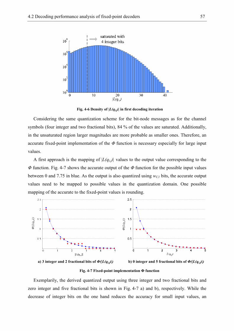
4.2 Decoding performance analysis of fixed-point decoders 57
Fig. 4-6 Density of |L(qi,j)| in first decoding iteration
Considering the same quantization scheme for the bit-node messages as for the channel
symbols (four integer and two fractional bits), 84 % of the values are saturated. Additionally,
in the unsaturated region larger magnitudes are more probable as smaller ones. Therefore, an
accurate fixed-point implementation of the Φ function is necessary especially for large input
values.
A first approach is the mapping of |L(qi,j)| values to the output value corresponding to the
Φ function. Fig. 4-7 shows the accurate output of the Φ function for the possible input values
between 0 and 7.75 in blue. As the output is also quantized using wC1 bits, the accurate output
values need to be mapped to possible values in the quantization domain. One possible
mapping of the accurate to the fixed-point values is rounding.
Φ(|L(q
i,j)|)
Φ(|L(q
i,j)|)
a) 3 integer and 2 fractional bits of Φ(|L(qi,j)|) b) 0 integer and 5 fractional bits of Φ(|L(qi,j)|)
Fig. 4-7 Fixed-point implementation Φ function
Exemplarily, the derived quantized output using three integer and two fractional bits and
zero integer and five fractional bits is shown in Fig. 4-7 a) and b), respectively. While the
decrease of integer bits on the one hand reduces the accuracy for small input values, an
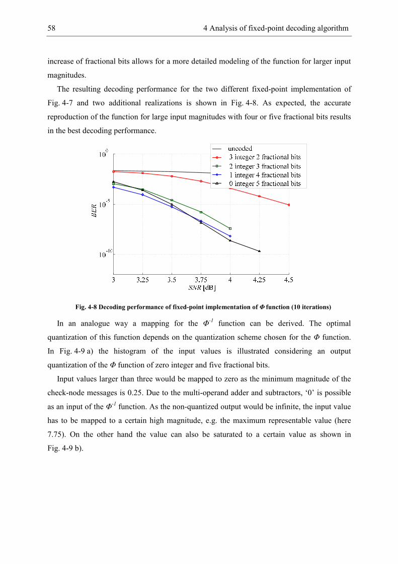
58 4 Analysis of fixed-point decoding algorithm
increase of fractional bits allows for a more detailed modeling of the function for larger input
magnitudes.
The resulting decoding performance for the two different fixed-point implementation of
Fig. 4-7 and two additional realizations is shown in Fig. 4-8. As expected, the accurate
reproduction of the function for large input magnitudes with four or five fractional bits results
in the best decoding performance.
Fig. 4-8 Decoding performance of fixed-point implementation of Φ function (10 iterations)
In an analogue way a mapping for the Φ-1 function can be derived. The optimal
quantization of this function depends on the quantization scheme chosen for the Φ function.
In Fig. 4-9 a) the histogram of the input values is illustrated considering an output
quantization of the Φ function of zero integer and five fractional bits.
Input values larger than three would be mapped to zero as the minimum magnitude of the
check-node messages is 0.25. Due to the multi-operand adder and subtractors, ‘0’ is possible
as an input of the Φ-1 function. As the non-quantized output would be infinite, the input value
has to be mapped to a certain high magnitude, e.g. the maximum representable value (here
7.75). On the other hand the value can also be saturated to a certain value as shown in
Fig. 4-9 b).
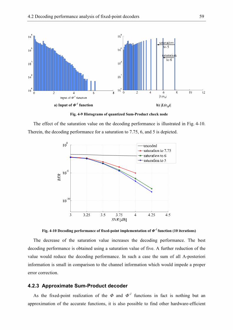
4.2 Decoding performance analysis of fixed-point decoders 59
a) Input of Φ-1 function b) |L(ri,j)|
Fig. 4-9 Histograms of quantized Sum-Product check node
The effect of the saturation value on the decoding performance is illustrated in Fig. 4-10.
Therein, the decoding performance for a saturation to 7.75, 6, and 5 is depicted.
Fig. 4-10 Decoding performance of fixed-point implementation of Φ-1 function (10 iterations)
The decrease of the saturation value increases the decoding performance. The best
decoding performance is obtained using a saturation value of five. A further reduction of the
value would reduce the decoding performance. In such a case the sum of all A-posteriori
information is small in comparison to the channel information which would impede a proper
error correction.
4.2.3 Approximate Sum-Product decoder
As the fixed-point realization of the Φ and Φ-1 functions in fact is nothing but an
approximation of the accurate functions, it is also possible to find other hardware-efficient
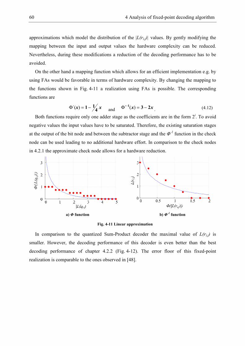
60 4 Analysis of fixed-point decoding algorithm
approximations which model the distribution of the |L(ri,j)| values. By gently modifying the
mapping between the input and output values the hardware complexity can be reduced.
Nevertheless, during these modifications a reduction of the decoding performance has to be
avoided.
On the other hand a mapping function which allows for an efficient implementation e.g. by
using FAs would be favorable in terms of hardware complexity. By changing the mapping to
the functions shown in Fig. 4-11 a realization using FAs is possible. The corresponding
functions are
xx411 −=Φ )´(
and xx 231 −=Φ − )(´. (4.12)
Both functions require only one adder stage as the coefficients are in the form 2i. To avoid
negative values the input values have to be saturated. Therefore, the existing saturation stages
at the output of the bit node and between the subtractor stage and the Φ-1 function in the check
node can be used leading to no additional hardware effort. In comparison to the check nodes
in 4.2.1 the approximate check node allows for a hardware reduction.
Ф(|L(q
i,j)|)
a) Φ function b) Φ-1 function
Fig. 4-11 Linear approximation
In comparison to the quantized Sum-Product decoder the maximal value of L(ri,j) is
smaller. However, the decoding performance of this decoder is even better than the best
decoding performance of chapter 4.2.2 (Fig. 4-12). The error floor of this fixed-point
realization is comparable to the ones observed in [48].
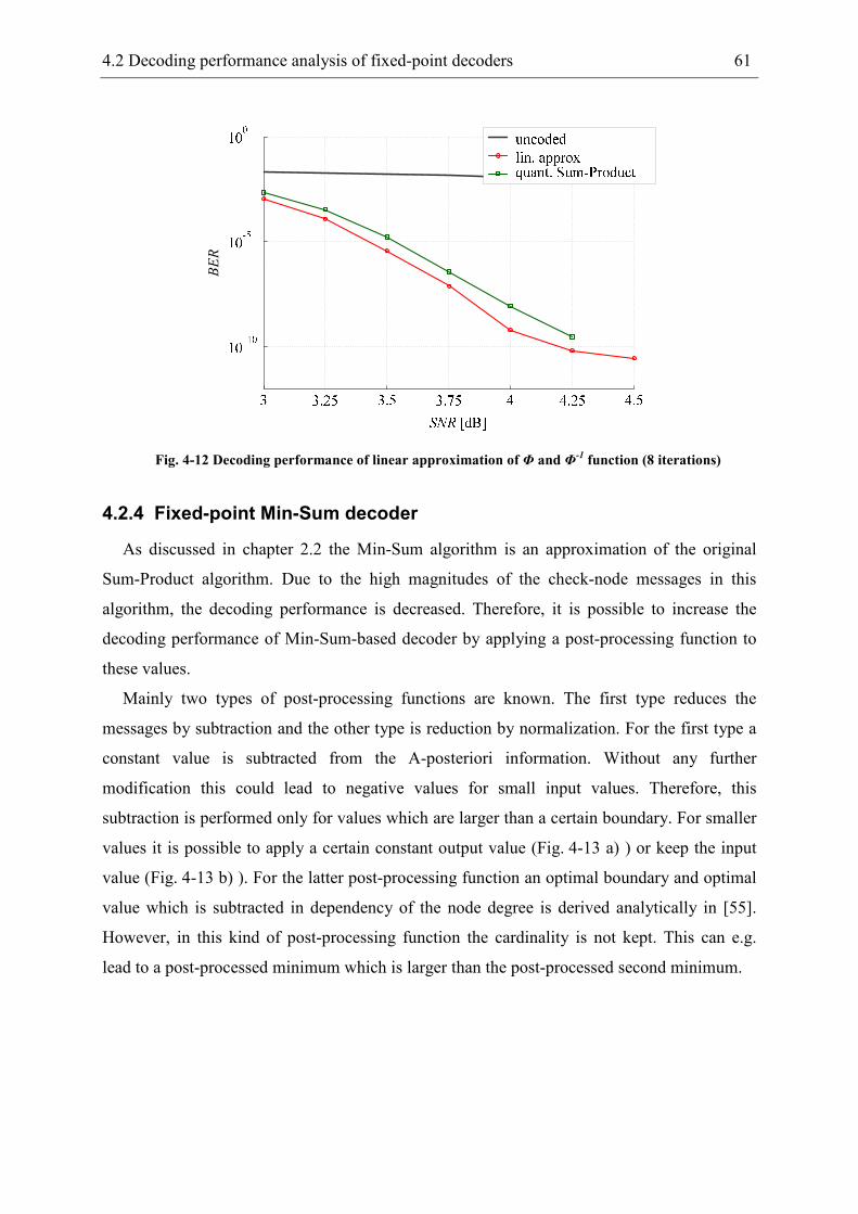
4.2 Decoding performance analysis of fixed-point decoders 61
BER
Fig. 4-12 Decoding performance of linear approximation of Φ and Φ-1 function (8 iterations)
4.2.4 Fixed-point Min-Sum decoder
As discussed in chapter 2.2 the Min-Sum algorithm is an approximation of the original
Sum-Product algorithm. Due to the high magnitudes of the check-node messages in this
algorithm, the decoding performance is decreased. Therefore, it is possible to increase the
decoding performance of Min-Sum-based decoder by applying a post-processing function to
these values.
Mainly two types of post-processing functions are known. The first type reduces the
messages by subtraction and the other type is reduction by normalization. For the first type a
constant value is subtracted from the A-posteriori information. Without any further
modification this could lead to negative values for small input values. Therefore, this
subtraction is performed only for values which are larger than a certain boundary. For smaller
values it is possible to apply a certain constant output value (Fig. 4-13 a) ) or keep the input
value (Fig. 4-13 b) ). For the latter post-processing function an optimal boundary and optimal
value which is subtracted in dependency of the node degree is derived analytically in [55].
However, in this kind of post-processing function the cardinality is not kept. This can e.g.
lead to a post-processed minimum which is larger than the post-processed second minimum.
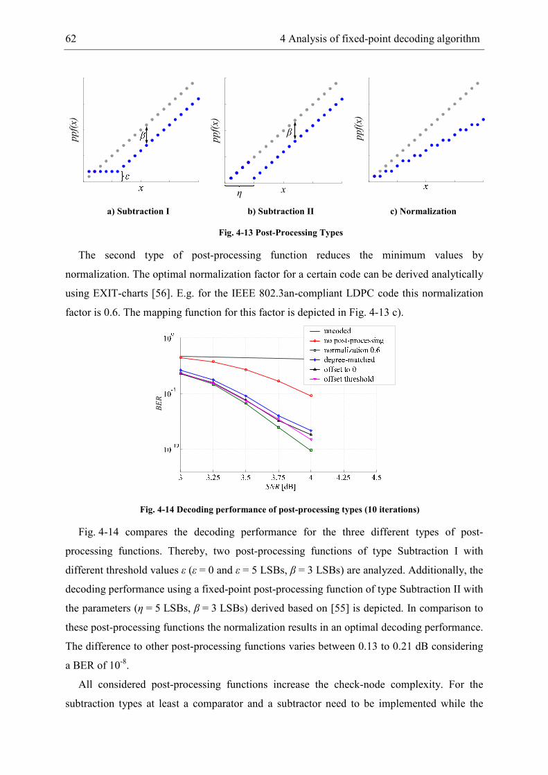
62 4 Analysis of fixed-point decoding algorithm
ppf(x)
η
β
ppf(x)
x
ppf(x)
a) Subtraction I b) Subtraction II c) Normalization
Fig. 4-13 Post-Processing Types
The second type of post-processing function reduces the minimum values by
normalization. The optimal normalization factor for a certain code can be derived analytically
using EXIT-charts [56]. E.g. for the IEEE 802.3an-compliant LDPC code this normalization
factor is 0.6. The mapping function for this factor is depicted in Fig. 4-13 c).
BER
Fig. 4-14 Decoding performance of post-processing types (10 iterations)
Fig. 4-14 compares the decoding performance for the three different types of post-
processing functions. Thereby, two post-processing functions of type Subtraction I with
different threshold values ε (ε = 0 and ε = 5 LSBs, β = 3 LSBs) are analyzed. Additionally, the
decoding performance using a fixed-point post-processing function of type Subtraction II with
the parameters (η = 5 LSBs, β = 3 LSBs) derived based on [55] is depicted. In comparison to
these post-processing functions the normalization results in an optimal decoding performance.
The difference to other post-processing functions varies between 0.13 to 0.21 dB considering
a BER of 10-8.
All considered post-processing functions increase the check-node complexity. For the
subtraction types at least a comparator and a subtractor need to be implemented while the
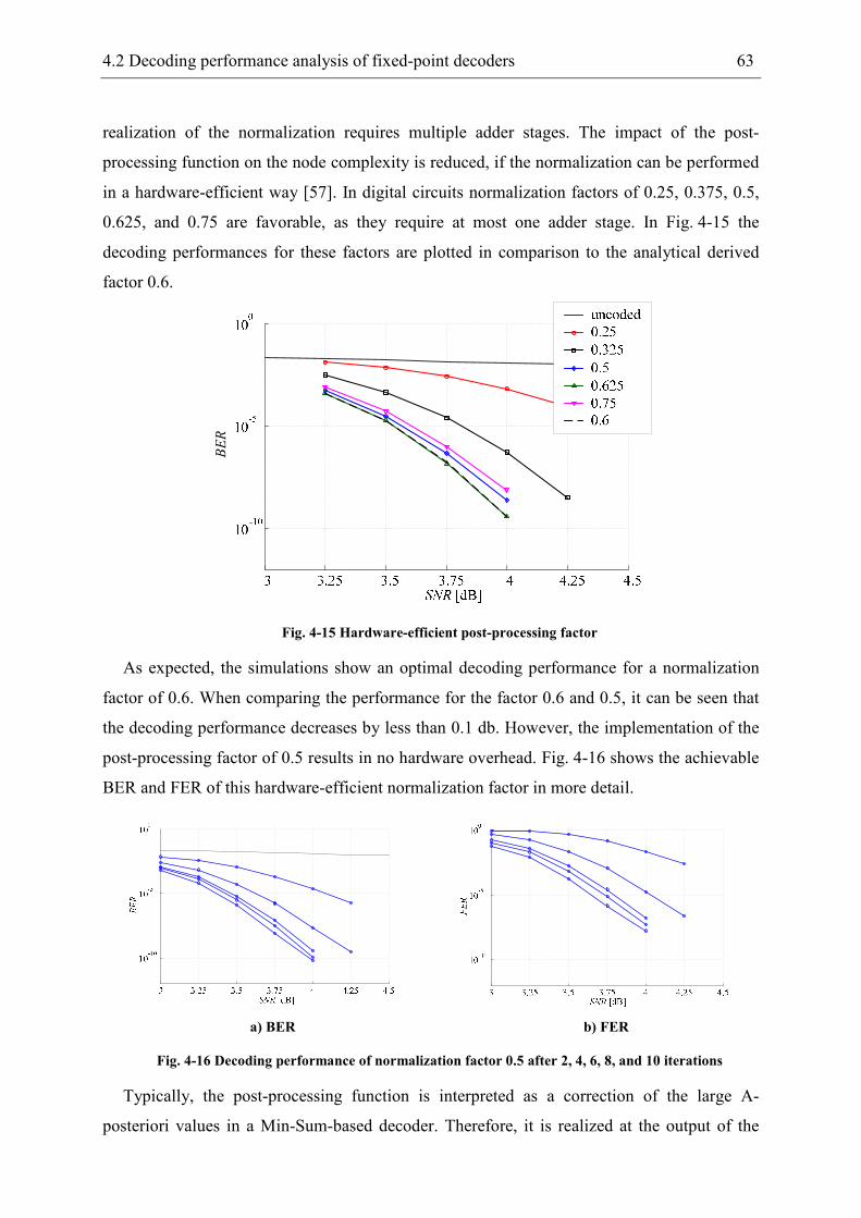
4.2 Decoding performance analysis of fixed-point decoders 63
realization of the normalization requires multiple adder stages. The impact of the post-
processing function on the node complexity is reduced, if the normalization can be performed
in a hardware-efficient way [57]. In digital circuits normalization factors of 0.25, 0.375, 0.5,
0.625, and 0.75 are favorable, as they require at most one adder stage. In Fig. 4-15 the
decoding performances for these factors are plotted in comparison to the analytical derived
factor 0.6.
BER
Fig. 4-15 Hardware-efficient post-processing factor
As expected, the simulations show an optimal decoding performance for a normalization
factor of 0.6. When comparing the performance for the factor 0.6 and 0.5, it can be seen that
the decoding performance decreases by less than 0.1 db. However, the implementation of the
post-processing factor of 0.5 results in no hardware overhead. Fig. 4-16 shows the achievable
BER and FER of this hardware-efficient normalization factor in more detail.
a) BER b) FER
Fig. 4-16 Decoding performance of normalization factor 0.5 after 2, 4, 6, 8, and 10 iterations
Typically, the post-processing function is interpreted as a correction of the large A-
posteriori values in a Min-Sum-based decoder. Therefore, it is realized at the output of the
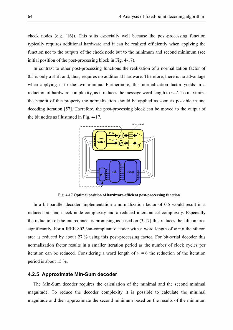
64 4 Analysis of fixed-point decoding algorithm
check nodes (e.g. [16]). This suits especially well because the post-processing function
typically requires additional hardware and it can be realized efficiently when applying the
function not to the outputs of the check node but to the minimum and second minimum (see
initial position of the post-processing block in Fig. 4-17).
In contrast to other post-processing functions the realization of a normalization factor of
0.5 is only a shift and, thus, requires no additional hardware. Therefore, there is no advantage
when applying it to the two minima. Furthermore, this normalization factor yields in a
reduction of hardware complexity, as it reduces the message word length to w-1. To maximize
the benefit of this property the normalization should be applied as soon as possible in one
decoding iteration [57]. Therefore, the post-processing block can be moved to the output of
the bit nodes as illustrated in Fig. 4-17.
Fig. 4-17 Optimal position of hardware-efficient post-processing function
In a bit-parallel decoder implementation a normalization factor of 0.5 would result in a
reduced bit- and check-node complexity and a reduced interconnect complexity. Especially
the reduction of the interconnect is promising as based on (3-17) this reduces the silicon area
significantly. For a IEEE 802.3an-compliant decoder with a word length of w = 6 the silicon
area is reduced by about 27 % using this post-processing factor. For bit-serial decoder this
normalization factor results in a smaller iteration period as the number of clock cycles per
iteration can be reduced. Considering a word length of w = 6 the reduction of the iteration
period is about 15 %.
4.2.5 Approximate Min-Sum decoder
The Min-Sum decoder requires the calculation of the minimal and the second minimal
magnitude. To reduce the decoder complexity it is possible to calculate the minimal
magnitude and then approximate the second minimum based on the results of the minimum
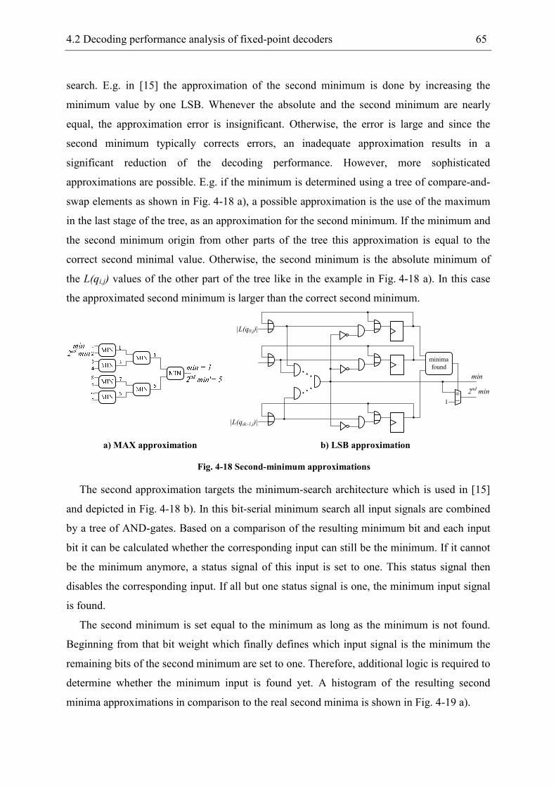
4.2 Decoding performance analysis of fixed-point decoders 65
search. E.g. in [15] the approximation of the second minimum is done by increasing the
minimum value by one LSB. Whenever the absolute and the second minimum are nearly
equal, the approximation error is insignificant. Otherwise, the error is large and since the
second minimum typically corrects errors, an inadequate approximation results in a
significant reduction of the decoding performance. However, more sophisticated
approximations are possible. E.g. if the minimum is determined using a tree of compare-and-
swap elements as shown in Fig. 4-18 a), a possible approximation is the use of the maximum
in the last stage of the tree, as an approximation for the second minimum. If the minimum and
the second minimum origin from other parts of the tree this approximation is equal to the
correct second minimal value. Otherwise, the second minimum is the absolute minimum of
the L(qi,j) values of the other part of the tree like in the example in Fig. 4-18 a). In this case
the approximated second minimum is larger than the correct second minimum.
|L(q0,j)|
|L(qdc-1,j)|
minima
found
1 0
min
1
2nd min
a) MAX approximation b) LSB approximation
Fig. 4-18 Second-minimum approximations
The second approximation targets the minimum-search architecture which is used in [15]
and depicted in Fig. 4-18 b). In this bit-serial minimum search all input signals are combined
by a tree of AND-gates. Based on a comparison of the resulting minimum bit and each input
bit it can be calculated whether the corresponding input can still be the minimum. If it cannot
be the minimum anymore, a status signal of this input is set to one. This status signal then
disables the corresponding input. If all but one status signal is one, the minimum input signal
is found.
The second minimum is set equal to the minimum as long as the minimum is not found.
Beginning from that bit weight which finally defines which input signal is the minimum the
remaining bits of the second minimum are set to one. Therefore, additional logic is required to
determine whether the minimum input is found yet. A histogram of the resulting second
minima approximations in comparison to the real second minima is shown in Fig. 4-19 a).
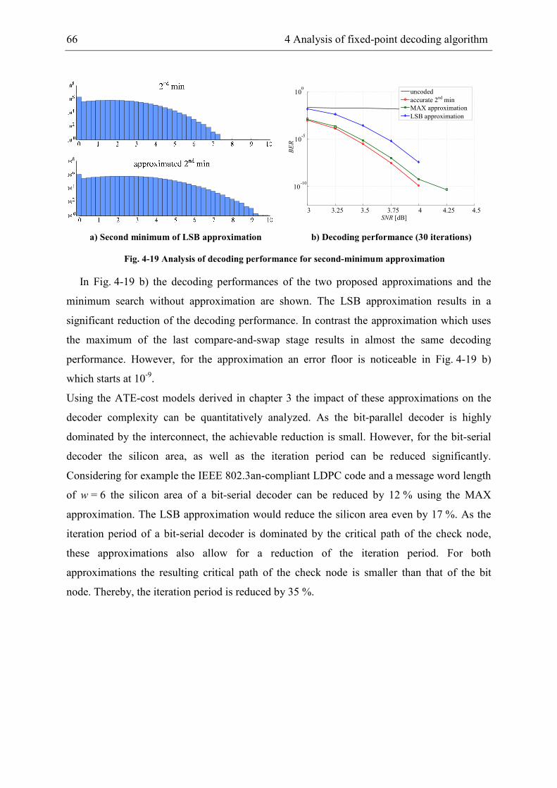
66 4 Analysis of fixed-point decoding algorithm
3 3.25 3.5 3.75 4 4.25 4.5
10-10
10-5
100
SNR [dB]
BER
uncoded
accurate 2nd min
MAX approximation
LSB approximation
a) Second minimum of LSB approximation b) Decoding performance (30 iterations)
Fig. 4-19 Analysis of decoding performance for second-minimum approximation
In Fig. 4-19 b) the decoding performances of the two proposed approximations and the
minimum search without approximation are shown. The LSB approximation results in a
significant reduction of the decoding performance. In contrast the approximation which uses
the maximum of the last compare-and-swap stage results in almost the same decoding
performance. However, for the approximation an error floor is noticeable in Fig. 4-19 b)
which starts at 10-9.
Using the ATE-cost models derived in chapter 3 the impact of these approximations on the
decoder complexity can be quantitatively analyzed. As the bit-parallel decoder is highly
dominated by the interconnect, the achievable reduction is small. However, for the bit-serial
decoder the silicon area, as well as the iteration period can be reduced significantly.
Considering for example the IEEE 802.3an-compliant LDPC code and a message word length
of w = 6 the silicon area of a bit-serial decoder can be reduced by 12 % using the MAX
approximation. The LSB approximation would reduce the silicon area even by 17 %. As the
iteration period of a bit-serial decoder is dominated by the critical path of the check node,
these approximations also allow for a reduction of the iteration period. For both
approximations the resulting critical path of the check node is smaller than that of the bit
node. Thereby, the iteration period is reduced by 35 %.
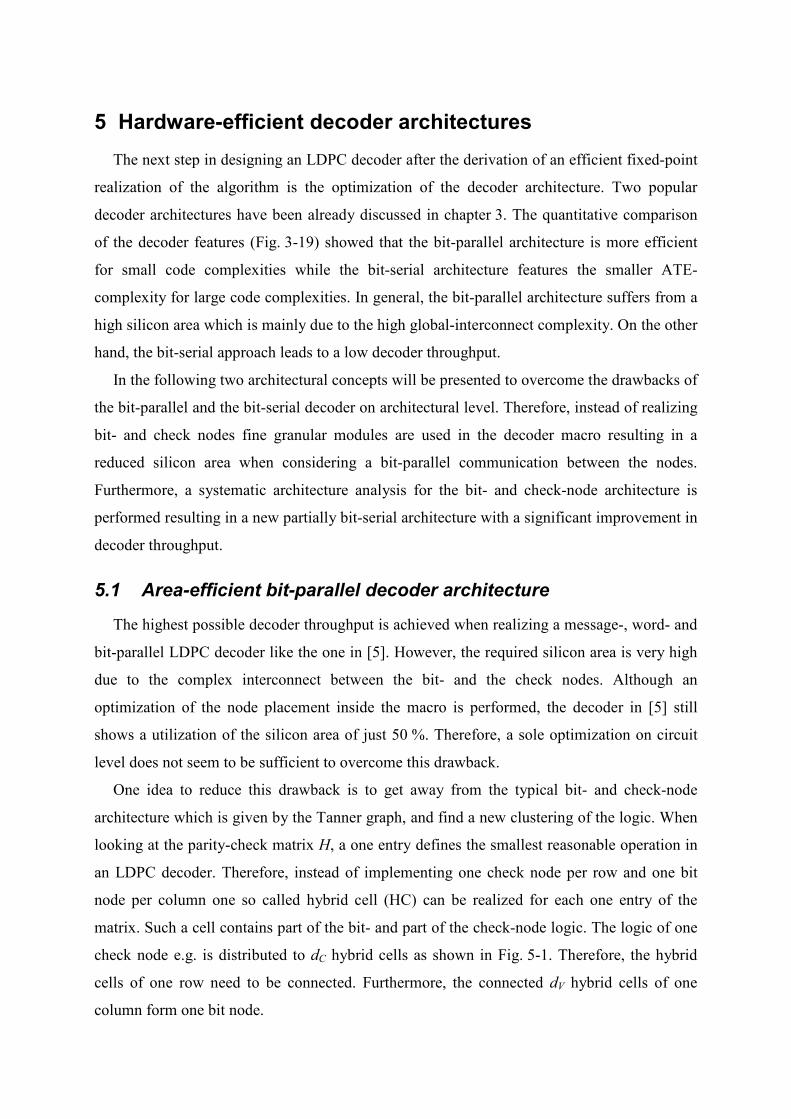
5 Hardware-efficient decoder architectures
The next step in designing an LDPC decoder after the derivation of an efficient fixed-point
realization of the algorithm is the optimization of the decoder architecture. Two popular
decoder architectures have been already discussed in chapter 3. The quantitative comparison
of the decoder features (Fig. 3-19) showed that the bit-parallel architecture is more efficient
for small code complexities while the bit-serial architecture features the smaller ATE-
complexity for large code complexities. In general, the bit-parallel architecture suffers from a
high silicon area which is mainly due to the high global-interconnect complexity. On the other
hand, the bit-serial approach leads to a low decoder throughput.
In the following two architectural concepts will be presented to overcome the drawbacks of
the bit-parallel and the bit-serial decoder on architectural level. Therefore, instead of realizing
bit- and check nodes fine granular modules are used in the decoder macro resulting in a
reduced silicon area when considering a bit-parallel communication between the nodes.
Furthermore, a systematic architecture analysis for the bit- and check-node architecture is
performed resulting in a new partially bit-serial architecture with a significant improvement in
decoder throughput.
5.1 Area-efficient bit-parallel decoder architecture
The highest possible decoder throughput is achieved when realizing a message-, word- and
bit-parallel LDPC decoder like the one in [5]. However, the required silicon area is very high
due to the complex interconnect between the bit- and the check nodes. Although an
optimization of the node placement inside the macro is performed, the decoder in [5] still
shows a utilization of the silicon area of just 50 %. Therefore, a sole optimization on circuit
level does not seem to be sufficient to overcome this drawback.
One idea to reduce this drawback is to get away from the typical bit- and check-node
architecture which is given by the Tanner graph, and find a new clustering of the logic. When
looking at the parity-check matrix H, a one entry defines the smallest reasonable operation in
an LDPC decoder. Therefore, instead of implementing one check node per row and one bit
node per column one so called hybrid cell (HC) can be realized for each one entry of the
matrix. Such a cell contains part of the bit- and part of the check-node logic. The logic of one
check node e.g. is distributed to dC hybrid cells as shown in Fig. 5-1. Therefore, the hybrid
cells of one row need to be connected. Furthermore, the connected dV hybrid cells of one
column form one bit node.
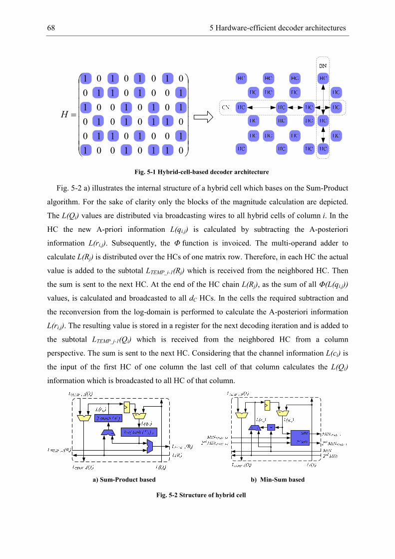
68 5 Hardware-efficient decoder architectures
=
01101001
10010110
01101010
10101001
10010110
01010101
H
Fig. 5-1 Hybrid-cell-based decoder architecture
Fig. 5-2 a) illustrates the internal structure of a hybrid cell which bases on the Sum-Product
algorithm. For the sake of clarity only the blocks of the magnitude calculation are depicted.
The L(Qi) values are distributed via broadcasting wires to all hybrid cells of column i. In the
HC the new A-priori information L(qi,j) is calculated by subtracting the A-posteriori
information L(ri,j). Subsequently, the Φ function is invoiced. The multi-operand adder to
calculate L(Rj) is distributed over the HCs of one matrix row. Therefore, in each HC the actual
value is added to the subtotal LTEMP_i-1(Rj) which is received from the neighbored HC. Then
the sum is sent to the next HC. At the end of the HC chain L(Rj), as the sum of all Φ(L(qi,j))
values, is calculated and broadcasted to all dC HCs. In the cells the required subtraction and
the reconversion from the log-domain is performed to calculate the A-posteriori information
L(ri,j). The resulting value is stored in a register for the next decoding iteration and is added to
the subtotal LTEMP_j-1(Qi) which is received from the neighbored HC from a column
perspective. The sum is sent to the next HC. Considering that the channel information L(ci) is
the input of the first HC of one column the last cell of that column calculates the L(Qi)
information which is broadcasted to all HC of that column.
a) Sum-Product based b) Min-Sum based
Fig. 5-2 Structure of hybrid cell
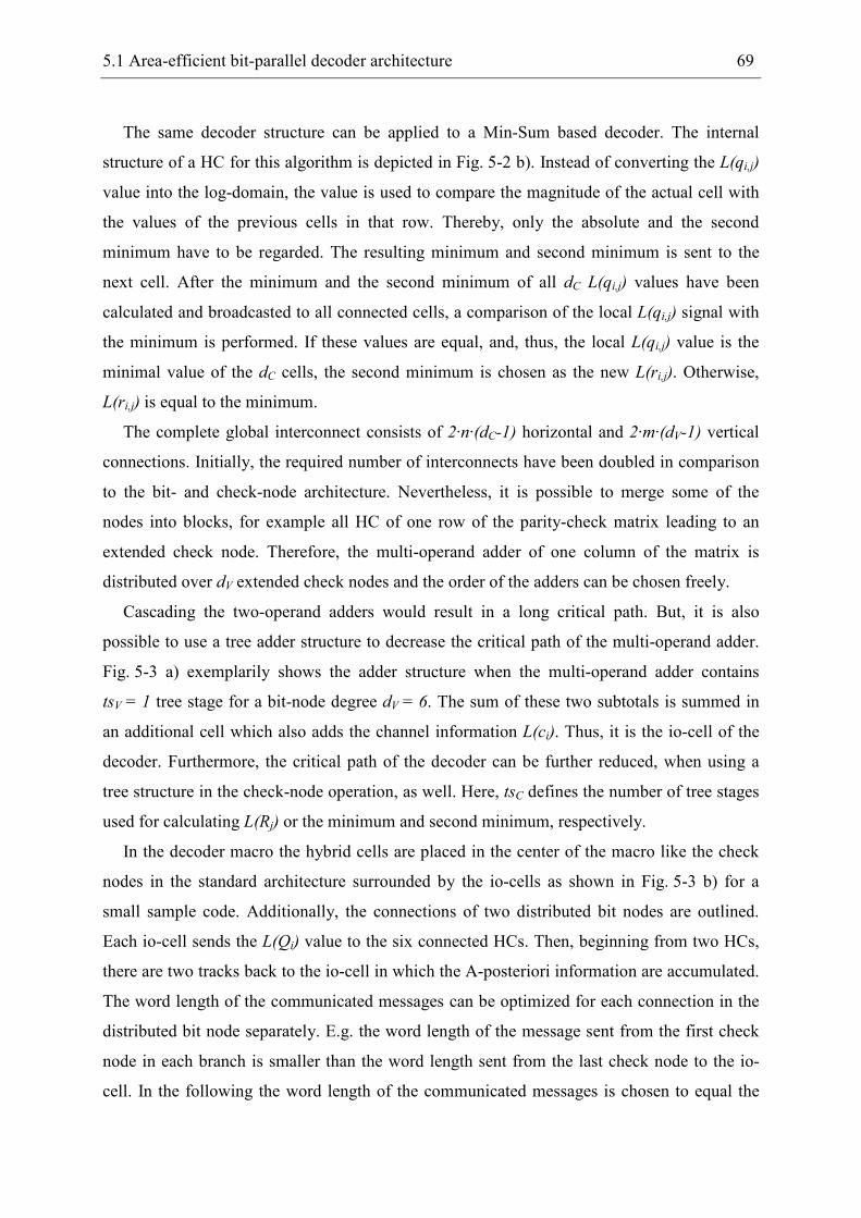
5.1 Area-efficient bit-parallel decoder architecture 69
The same decoder structure can be applied to a Min-Sum based decoder. The internal
structure of a HC for this algorithm is depicted in Fig. 5-2 b). Instead of converting the L(qi,j)
value into the log-domain, the value is used to compare the magnitude of the actual cell with
the values of the previous cells in that row. Thereby, only the absolute and the second
minimum have to be regarded. The resulting minimum and second minimum is sent to the
next cell. After the minimum and the second minimum of all dC L(qi,j) values have been
calculated and broadcasted to all connected cells, a comparison of the local L(qi,j) signal with
the minimum is performed. If these values are equal, and, thus, the local L(qi,j) value is the
minimal value of the dC cells, the second minimum is chosen as the new L(ri,j). Otherwise,
L(ri,j) is equal to the minimum.
The complete global interconnect consists of 2·n·(dC-1) horizontal and 2·m·(dV-1) vertical
connections. Initially, the required number of interconnects have been doubled in comparison
to the bit- and check-node architecture. Nevertheless, it is possible to merge some of the
nodes into blocks, for example all HC of one row of the parity-check matrix leading to an
extended check node. Therefore, the multi-operand adder of one column of the matrix is
distributed over dV extended check nodes and the order of the adders can be chosen freely.
Cascading the two-operand adders would result in a long critical path. But, it is also
possible to use a tree adder structure to decrease the critical path of the multi-operand adder.
Fig. 5-3 a) exemplarily shows the adder structure when the multi-operand adder contains
tsV = 1 tree stage for a bit-node degree dV = 6. The sum of these two subtotals is summed in
an additional cell which also adds the channel information L(ci). Thus, it is the io-cell of the
decoder. Furthermore, the critical path of the decoder can be further reduced, when using a
tree structure in the check-node operation, as well. Here, tsC defines the number of tree stages
used for calculating L(Rj) or the minimum and second minimum, respectively.
In the decoder macro the hybrid cells are placed in the center of the macro like the check
nodes in the standard architecture surrounded by the io-cells as shown in Fig. 5-3 b) for a
small sample code. Additionally, the connections of two distributed bit nodes are outlined.
Each io-cell sends the L(Qi) value to the six connected HCs. Then, beginning from two HCs,
there are two tracks back to the io-cell in which the A-posteriori information are accumulated.
The word length of the communicated messages can be optimized for each connection in the
distributed bit node separately. E.g. the word length of the message sent from the first check
node in each branch is smaller than the word length sent from the last check node to the io-
cell. In the following the word length of the communicated messages is chosen to equal the
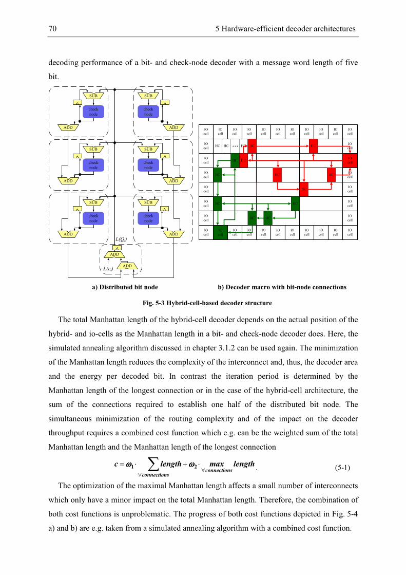
70 5 Hardware-efficient decoder architectures
decoding performance of a bit- and check-node decoder with a message word length of five
bit.
ADD
SUB
check
node
ADD
SUB
check
node
ADD
SUB
check
node
ADD
SUB
check
node
ADD
SUB
check
node
ADD
SUB
check
node
ADD
ADD
L(Qi)
L(ci)
HC HC HC
IO
cell
IO
cell
IO
cell
IO
cell
IO
cell
IO
cell
IO
cell
IO
cell
IO
cell
IO
cell
IO
cell
IO
cell
IO
cell
IO
cell
IO
cell
IO
cell
IO
cell
IO
cell
IO
cell
IO
cell
IO
cell
IO
cell
IO
cell
IO
cell
IO
cell
IO
cell
IO
cell
IO
cell
IO
cell
IO
cell
IO
cell
IO
cell
IO
cell
HC
IO
cell
HC
HC
HC
HC
HC
HC
HCHC
HC
HC
HC
a) Distributed bit node b) Decoder macro with bit-node connections
Fig. 5-3 Hybrid-cell-based decoder structure
The total Manhattan length of the hybrid-cell decoder depends on the actual position of the
hybrid- and io-cells as the Manhattan length in a bit- and check-node decoder does. Here, the
simulated annealing algorithm discussed in chapter 3.1.2 can be used again. The minimization
of the Manhattan length reduces the complexity of the interconnect and, thus, the decoder area
and the energy per decoded bit. In contrast the iteration period is determined by the
Manhattan length of the longest connection or in the case of the hybrid-cell architecture, the
sum of the connections required to establish one half of the distributed bit node. The
simultaneous minimization of the routing complexity and of the impact on the decoder
throughput requires a combined cost function which e.g. can be the weighted sum of the total
Manhattan length and the Manhattan length of the longest connection
lengthmaxlengthcsconnection
sconnection∀
∀
⋅+⋅= ∑ 21 ωωωωωωωω . (5-1)
The optimization of the maximal Manhattan length affects a small number of interconnects
which only have a minor impact on the total Manhattan length. Therefore, the combination of
both cost functions is unproblematic. The progress of both cost functions depicted in Fig. 5-4
a) and b) are e.g. taken from a simulated annealing algorithm with a combined cost function.
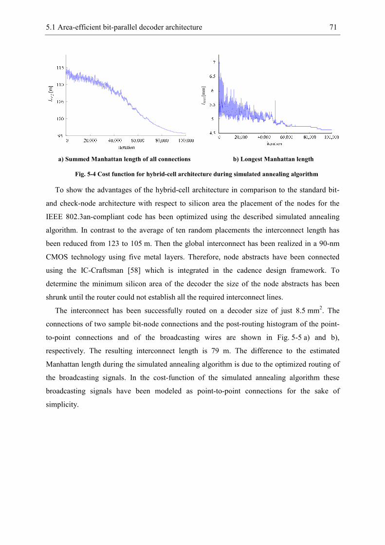
5.1 Area-efficient bit-parallel decoder architecture 71
l MAX [mm]
a) Summed Manhattan length of all connections b) Longest Manhattan length
Fig. 5-4 Cost function for hybrid-cell architecture during simulated annealing algorithm
To show the advantages of the hybrid-cell architecture in comparison to the standard bit-
and check-node architecture with respect to silicon area the placement of the nodes for the
IEEE 802.3an-compliant code has been optimized using the described simulated annealing
algorithm. In contrast to the average of ten random placements the interconnect length has
been reduced from 123 to 105 m. Then the global interconnect has been realized in a 90-nm
CMOS technology using five metal layers. Therefore, node abstracts have been connected
using the IC-Craftsman [58] which is integrated in the cadence design framework. To
determine the minimum silicon area of the decoder the size of the node abstracts has been
shrunk until the router could not establish all the required interconnect lines.
The interconnect has been successfully routed on a decoder size of just 8.5 mm2. The
connections of two sample bit-node connections and the post-routing histogram of the point-
to-point connections and of the broadcasting wires are shown in Fig. 5-5 a) and b),
respectively. The resulting interconnect length is 79 m. The difference to the estimated
Manhattan length during the simulated annealing algorithm is due to the optimized routing of
the broadcasting signals. In the cost-function of the simulated annealing algorithm these
broadcasting signals have been modeled as point-to-point connections for the sake of
simplicity.
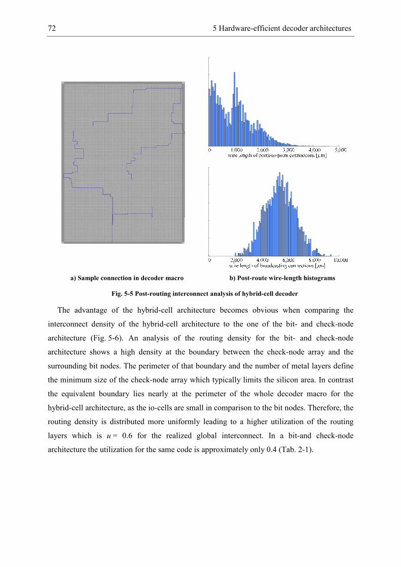
72 5 Hardware-efficient decoder architectures
a) Sample connection in decoder macro b) Post-route wire-length histograms
Fig. 5-5 Post-routing interconnect analysis of hybrid-cell decoder
The advantage of the hybrid-cell architecture becomes obvious when comparing the
interconnect density of the hybrid-cell architecture to the one of the bit- and check-node
architecture (Fig. 5-6). An analysis of the routing density for the bit- and check-node
architecture shows a high density at the boundary between the check-node array and the
surrounding bit nodes. The perimeter of that boundary and the number of metal layers define
the minimum size of the check-node array which typically limits the silicon area. In contrast
the equivalent boundary lies nearly at the perimeter of the whole decoder macro for the
hybrid-cell architecture, as the io-cells are small in comparison to the bit nodes. Therefore, the
routing density is distributed more uniformly leading to a higher utilization of the routing
layers which is u = 0.6 for the realized global interconnect. In a bit-and check-node
architecture the utilization for the same code is approximately only 0.4 (Tab. 2-1).
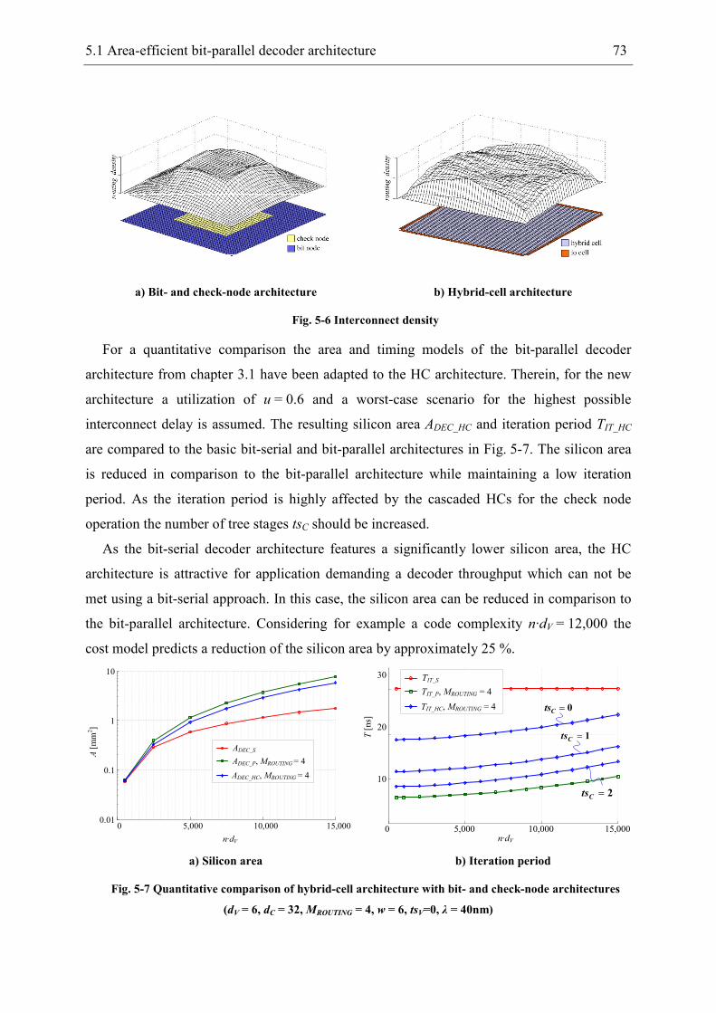
5.1 Area-efficient bit-parallel decoder architecture 73
a) Bit- and check-node architecture b) Hybrid-cell architecture
Fig. 5-6 Interconnect density
For a quantitative comparison the area and timing models of the bit-parallel decoder
architecture from chapter 3.1 have been adapted to the HC architecture. Therein, for the new
architecture a utilization of u = 0.6 and a worst-case scenario for the highest possible
interconnect delay is assumed. The resulting silicon area ADEC_HC and iteration period TIT_HC
are compared to the basic bit-serial and bit-parallel architectures in Fig. 5-7. The silicon area
is reduced in comparison to the bit-parallel architecture while maintaining a low iteration
period. As the iteration period is highly affected by the cascaded HCs for the check node
operation the number of tree stages tsC should be increased.
As the bit-serial decoder architecture features a significantly lower silicon area, the HC
architecture is attractive for application demanding a decoder throughput which can not be
met using a bit-serial approach. In this case, the silicon area can be reduced in comparison to
the bit-parallel architecture. Considering for example a code complexity n·dV = 12,000 the
cost model predicts a reduction of the silicon area by approximately 25 %.
0 5,000 10,000 15,0000.01
0.1
1
10
A[mm2]
ADEC_S
ADEC_P, MROUTING = 4
ADEC_HC, MROUTING = 4
n·dV
TIT_S
TIT_P, MROUTING = 4
TIT_HC, MROUTING = 4
0 5,000 10,000 15,000
10
20
30
n·dV
T[ns]
0=Cts
1=Cts
2=Cts
a) Silicon area b) Iteration period
Fig. 5-7 Quantitative comparison of hybrid-cell architecture with bit- and check-node architectures
(dV = 6, dC = 32, MROUTING = 4, w = 6, tsV=0, λ = 40nm)
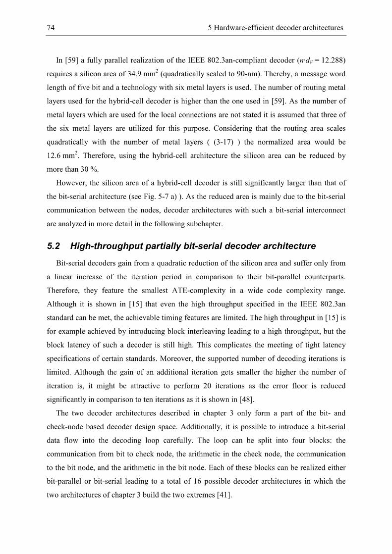
74 5 Hardware-efficient decoder architectures
In [59] a fully parallel realization of the IEEE 802.3an-compliant decoder (n·dV = 12.288)
requires a silicon area of 34.9 mm2 (quadratically scaled to 90-nm). Thereby, a message word
length of five bit and a technology with six metal layers is used. The number of routing metal
layers used for the hybrid-cell decoder is higher than the one used in [59]. As the number of
metal layers which are used for the local connections are not stated it is assumed that three of
the six metal layers are utilized for this purpose. Considering that the routing area scales
quadratically with the number of metal layers ( (3-17) ) the normalized area would be
12.6 mm2. Therefore, using the hybrid-cell architecture the silicon area can be reduced by
more than 30 %.
However, the silicon area of a hybrid-cell decoder is still significantly larger than that of
the bit-serial architecture (see Fig. 5-7 a) ). As the reduced area is mainly due to the bit-serial
communication between the nodes, decoder architectures with such a bit-serial interconnect
are analyzed in more detail in the following subchapter.
5.2 High-throughput partially bit-serial decoder architecture
Bit-serial decoders gain from a quadratic reduction of the silicon area and suffer only from
a linear increase of the iteration period in comparison to their bit-parallel counterparts.
Therefore, they feature the smallest ATE-complexity in a wide code complexity range.
Although it is shown in [15] that even the high throughput specified in the IEEE 802.3an
standard can be met, the achievable timing features are limited. The high throughput in [15] is
for example achieved by introducing block interleaving leading to a high throughput, but the
block latency of such a decoder is still high. This complicates the meeting of tight latency
specifications of certain standards. Moreover, the supported number of decoding iterations is
limited. Although the gain of an additional iteration gets smaller the higher the number of
iteration is, it might be attractive to perform 20 iterations as the error floor is reduced
significantly in comparison to ten iterations as it is shown in [48].
The two decoder architectures described in chapter 3 only form a part of the bit- and
check-node based decoder design space. Additionally, it is possible to introduce a bit-serial
data flow into the decoding loop carefully. The loop can be split into four blocks: the
communication from bit to check node, the arithmetic in the check node, the communication
to the bit node, and the arithmetic in the bit node. Each of these blocks can be realized either
bit-parallel or bit-serial leading to a total of 16 possible decoder architectures in which the
two architectures of chapter 3 build the two extremes [41].
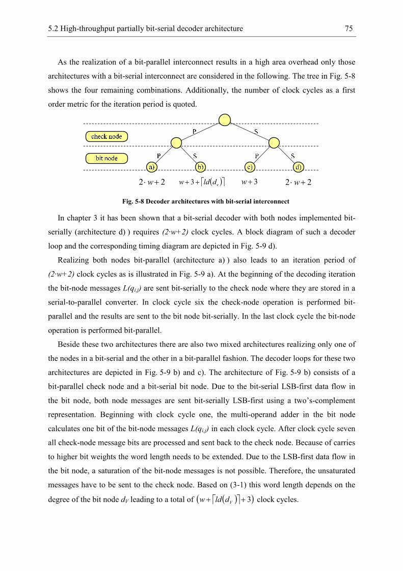
5.2 High-throughput partially bit-serial decoder architecture 75
As the realization of a bit-parallel interconnect results in a high area overhead only those
architectures with a bit-serial interconnect are considered in the following. The tree in Fig. 5-8
shows the four remaining combinations. Additionally, the number of clock cycles as a first
order metric for the iteration period is quoted.
22 +⋅w3+w22 +⋅w ( ) vdldw ++ 3
Fig. 5-8 Decoder architectures with bit-serial interconnect
In chapter 3 it has been shown that a bit-serial decoder with both nodes implemented bit-
serially (architecture d) ) requires (2·w+2) clock cycles. A block diagram of such a decoder
loop and the corresponding timing diagram are depicted in Fig. 5-9 d).
Realizing both nodes bit-parallel (architecture a) ) also leads to an iteration period of
(2·w+2) clock cycles as is illustrated in Fig. 5-9 a). At the beginning of the decoding iteration
the bit-node messages L(qi,j) are sent bit-serially to the check node where they are stored in a
serial-to-parallel converter. In clock cycle six the check-node operation is performed bit-
parallel and the results are sent to the bit node bit-serially. In the last clock cycle the bit-node
operation is performed bit-parallel.
Beside these two architectures there are also two mixed architectures realizing only one of
the nodes in a bit-serial and the other in a bit-parallel fashion. The decoder loops for these two
architectures are depicted in Fig. 5-9 b) and c). The architecture of Fig. 5-9 b) consists of a
bit-parallel check node and a bit-serial bit node. Due to the bit-serial LSB-first data flow in
the bit node, both node messages are sent bit-serially LSB-first using a two’s-complement
representation. Beginning with clock cycle one, the multi-operand adder in the bit node
calculates one bit of the bit-node messages L(qi,j) in each clock cycle. After clock cycle seven
all check-node message bits are processed and sent back to the check node. Because of carries
to higher bit weights the word length needs to be extended. Due to the LSB-first data flow in
the bit node, a saturation of the bit-node messages is not possible. Therefore, the unsaturated
messages have to be sent to the check node. Based on (3-1) this word length depends on the
degree of the bit node dV leading to a total of ( ) ( )3++ Vdldw clock cycles.
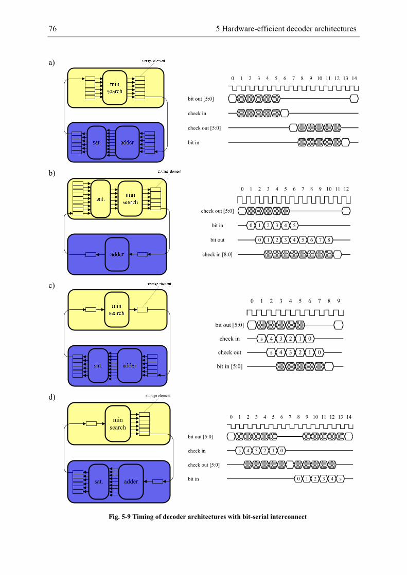
76 5 Hardware-efficient decoder architectures
a)
0 1 2 3 84 5 6 7
bit out [5:0]
check out [5:0]
check in
bit in
12 139 10 11 14
b)
0 1 2 3 9 10 114 5 6 7 8
check out [5:0]
12
bit out 8
bit in 0 1 2 3 4 5
check in [8:0]
4 5 6 70 1 2 3
c)
8 94 5 6 70 1 2 3
bit out [5:0]
0
check in
check out
bit in [5:0]
1 0
s 4 3 2 1
s 4 3 2
d)
adder
min
search
sat.
storage element
9 10 11 1412 13
0 4 s1 2bit in 3
check out [5:0]
2 1 0check in s 4 3
bit out [5:0]
84 5 6 70 1 2 3
Fig. 5-9 Timing of decoder architectures with bit-serial interconnect
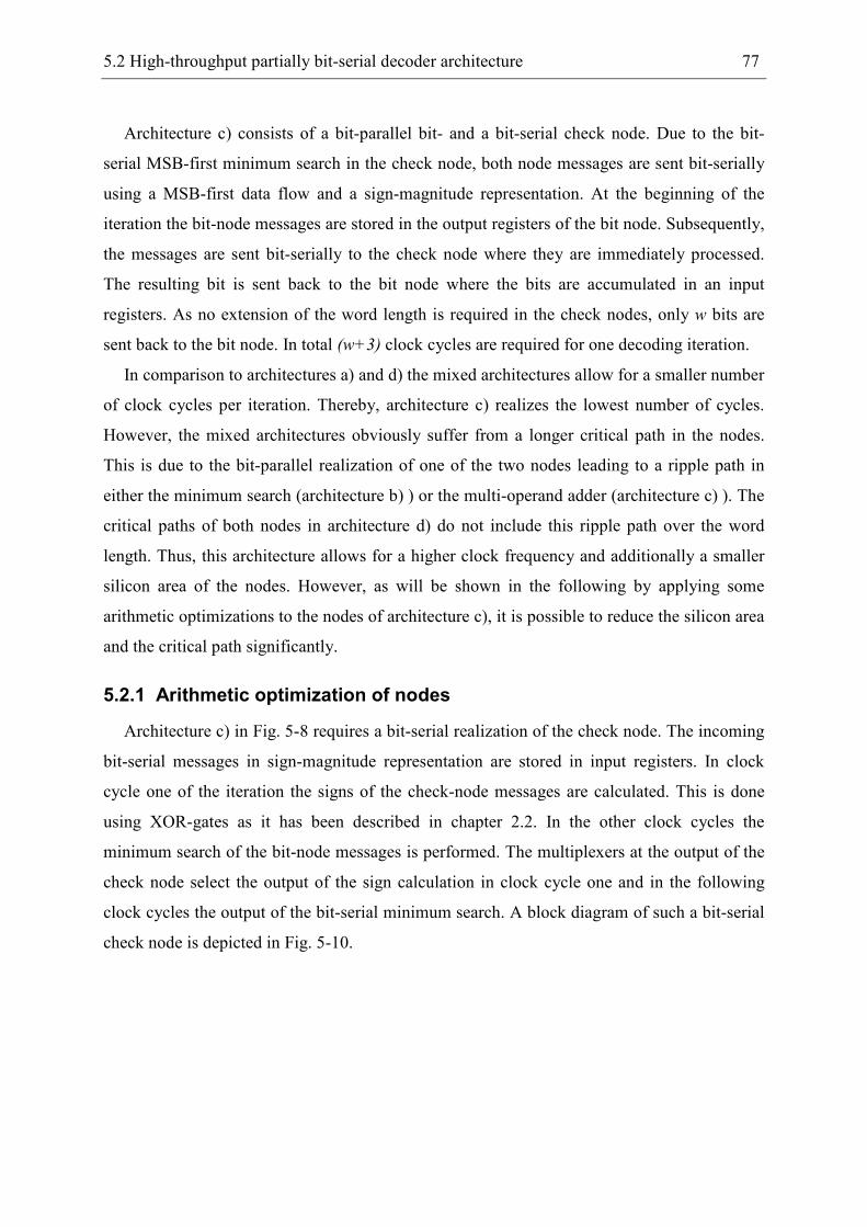
5.2 High-throughput partially bit-serial decoder architecture 77
Architecture c) consists of a bit-parallel bit- and a bit-serial check node. Due to the bit-
serial MSB-first minimum search in the check node, both node messages are sent bit-serially
using a MSB-first data flow and a sign-magnitude representation. At the beginning of the
iteration the bit-node messages are stored in the output registers of the bit node. Subsequently,
the messages are sent bit-serially to the check node where they are immediately processed.
The resulting bit is sent back to the bit node where the bits are accumulated in an input
registers. As no extension of the word length is required in the check nodes, only w bits are
sent back to the bit node. In total (w+3) clock cycles are required for one decoding iteration.
In comparison to architectures a) and d) the mixed architectures allow for a smaller number
of clock cycles per iteration. Thereby, architecture c) realizes the lowest number of cycles.
However, the mixed architectures obviously suffer from a longer critical path in the nodes.
This is due to the bit-parallel realization of one of the two nodes leading to a ripple path in
either the minimum search (architecture b) ) or the multi-operand adder (architecture c) ). The
critical paths of both nodes in architecture d) do not include this ripple path over the word
length. Thus, this architecture allows for a higher clock frequency and additionally a smaller
silicon area of the nodes. However, as will be shown in the following by applying some
arithmetic optimizations to the nodes of architecture c), it is possible to reduce the silicon area
and the critical path significantly.
5.2.1 Arithmetic optimization of nodes
Architecture c) in Fig. 5-8 requires a bit-serial realization of the check node. The incoming
bit-serial messages in sign-magnitude representation are stored in input registers. In clock
cycle one of the iteration the signs of the check-node messages are calculated. This is done
using XOR-gates as it has been described in chapter 2.2. In the other clock cycles the
minimum search of the bit-node messages is performed. The multiplexers at the output of the
check node select the output of the sign calculation in clock cycle one and in the following
clock cycles the output of the bit-serial minimum search. A block diagram of such a bit-serial
check node is depicted in Fig. 5-10.
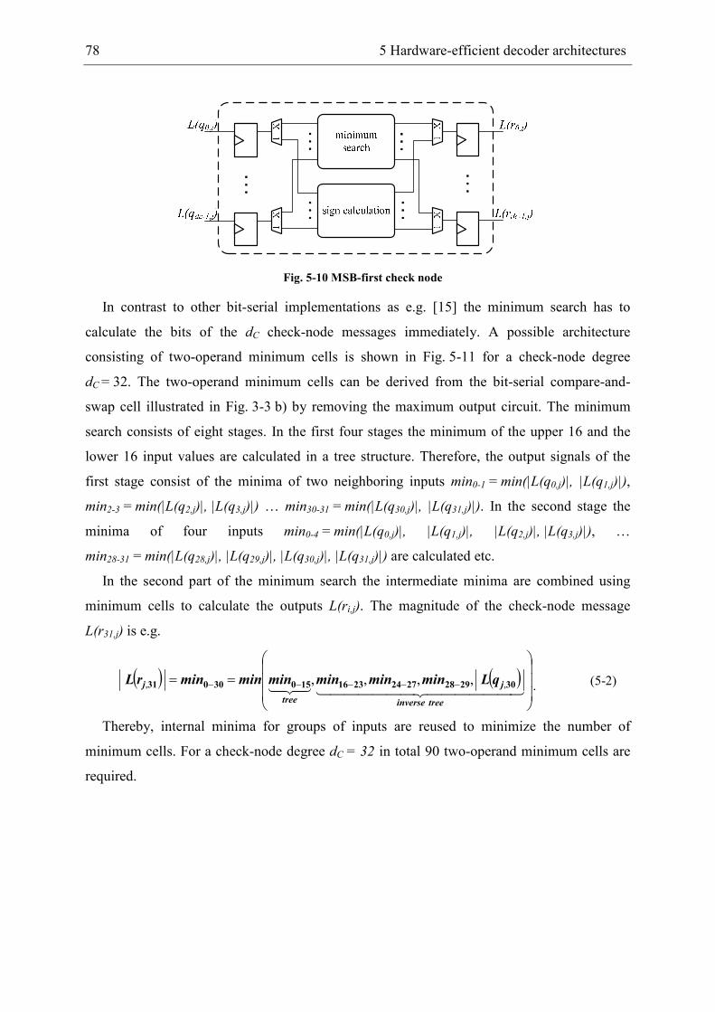
78 5 Hardware-efficient decoder architectures
Fig. 5-10 MSB-first check node
In contrast to other bit-serial implementations as e.g. [15] the minimum search has to
calculate the bits of the dC check-node messages immediately. A possible architecture
consisting of two-operand minimum cells is shown in Fig. 5-11 for a check-node degree
dC = 32. The two-operand minimum cells can be derived from the bit-serial compare-and-
swap cell illustrated in Fig. 3-3 b) by removing the maximum output circuit. The minimum
search consists of eight stages. In the first four stages the minimum of the upper 16 and the
lower 16 input values are calculated in a tree structure. Therefore, the output signals of the
first stage consist of the minima of two neighboring inputs min0-1 = min(|L(q0,j)|, |L(q1,j)|),
min2-3 = min(|L(q2,j)|, |L(q3,j)|) … min30-31 = min(|L(q30,j)|, |L(q31,j)|). In the second stage the
minima of four inputs min0-4 = min(|L(q0,j)|, |L(q1,j)|, |L(q2,j)|, |L(q3,j)|), …
min28-31 = min(|L(q28,j)|, |L(q29,j)|, |L(q30,j)|, |L(q31,j)|) are calculated etc.
In the second part of the minimum search the intermediate minima are combined using
minimum cells to calculate the outputs L(ri,j). The magnitude of the check-node message
L(r31,j) is e.g.
( ) ( )
== −−−−−444444 3444444 2143421
treeinverse
j
tree
j qLminminminminminminrL 3029282724231615030031 ,, ,,,,.
(5-2)
Thereby, internal minima for groups of inputs are reused to minimize the number of
minimum cells. For a check-node degree dC = 32 in total 90 two-operand minimum cells are
required.
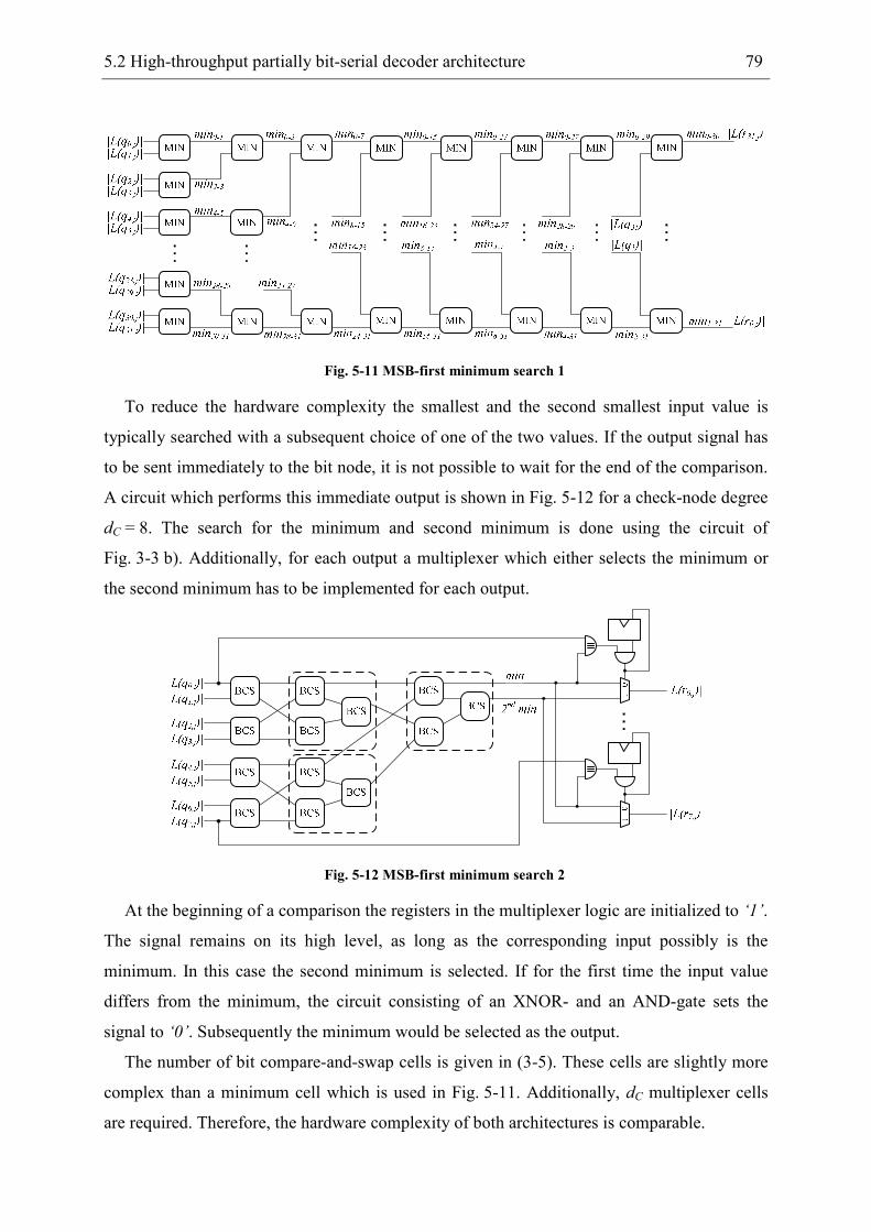
5.2 High-throughput partially bit-serial decoder architecture 79
Fig. 5-11 MSB-first minimum search 1
To reduce the hardware complexity the smallest and the second smallest input value is
typically searched with a subsequent choice of one of the two values. If the output signal has
to be sent immediately to the bit node, it is not possible to wait for the end of the comparison.
A circuit which performs this immediate output is shown in Fig. 5-12 for a check-node degree
dC = 8. The search for the minimum and second minimum is done using the circuit of
Fig. 3-3 b). Additionally, for each output a multiplexer which either selects the minimum or
the second minimum has to be implemented for each output.
Fig. 5-12 MSB-first minimum search 2
At the beginning of a comparison the registers in the multiplexer logic are initialized to ‘1’.
The signal remains on its high level, as long as the corresponding input possibly is the
minimum. In this case the second minimum is selected. If for the first time the input value
differs from the minimum, the circuit consisting of an XNOR- and an AND-gate sets the
signal to ‘0’. Subsequently the minimum would be selected as the output.
The number of bit compare-and-swap cells is given in (3-5). These cells are slightly more
complex than a minimum cell which is used in Fig. 5-11. Additionally, dC multiplexer cells
are required. Therefore, the hardware complexity of both architectures is comparable.
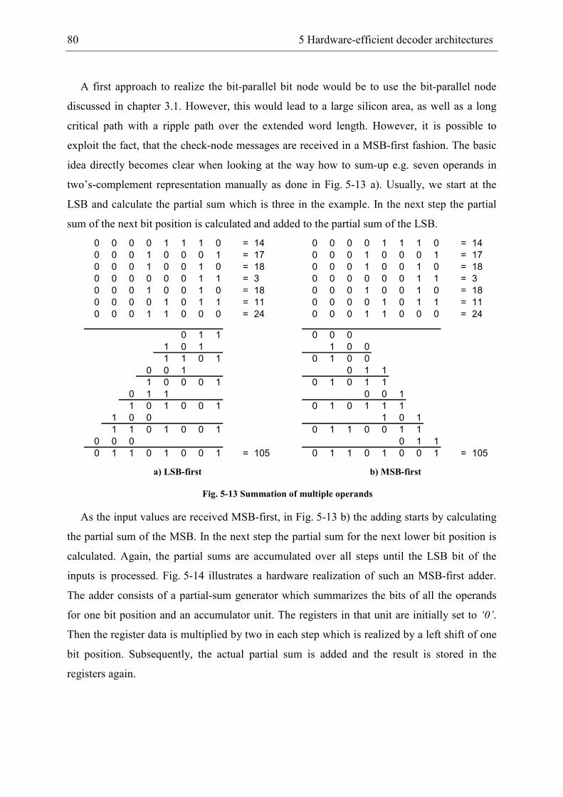
80 5 Hardware-efficient decoder architectures
A first approach to realize the bit-parallel bit node would be to use the bit-parallel node
discussed in chapter 3.1. However, this would lead to a large silicon area, as well as a long
critical path with a ripple path over the extended word length. However, it is possible to
exploit the fact, that the check-node messages are received in a MSB-first fashion. The basic
idea directly becomes clear when looking at the way how to sum-up e.g. seven operands in
two’s-complement representation manually as done in Fig. 5-13 a). Usually, we start at the
LSB and calculate the partial sum which is three in the example. In the next step the partial
sum of the next bit position is calculated and added to the partial sum of the LSB.
0 0 0 0 1 1 1 0 = 14
0 0 0 1 0 0 0 1 = 17
0 0 0 1 0 0 1 0 = 18
0 0 0 0 0 0 1 1 = 3
0 0 0 1 0 0 1 0 = 18
0 0 0 0 1 0 1 1 = 11
0 0 0 1 1 0 0 0 = 24
0 1 1
1 0 1
1 1 0 1
0 0 1
1 0 0 0 1
0 1 1
1 0 1 0 0 1
1 0 0
1 1 0 1 0 0 1
0 0 0
0 1 1 0 1 0 0 1 = 105
0 0 0 0 1 1 1 0 = 14
0 0 0 1 0 0 0 1 = 17
0 0 0 1 0 0 1 0 = 18
0 0 0 0 0 0 1 1 = 3
0 0 0 1 0 0 1 0 = 18
0 0 0 0 1 0 1 1 = 11
0 0 0 1 1 0 0 0 = 24
0 0 0
1 0 0
0 1 0 0
0 1 1
0 1 0 1 1
0 0 1
0 1 0 1 1 1
1 0 1
0 1 1 0 0 1 1
0 1 1
0 1 1 0 1 0 0 1 = 105
a) LSB-first b) MSB-first
Fig. 5-13 Summation of multiple operands
As the input values are received MSB-first, in Fig. 5-13 b) the adding starts by calculating
the partial sum of the MSB. In the next step the partial sum for the next lower bit position is
calculated. Again, the partial sums are accumulated over all steps until the LSB bit of the
inputs is processed. Fig. 5-14 illustrates a hardware realization of such an MSB-first adder.
The adder consists of a partial-sum generator which summarizes the bits of all the operands
for one bit position and an accumulator unit. The registers in that unit are initially set to ‘0’.
Then the register data is multiplied by two in each step which is realized by a left shift of one
bit position. Subsequently, the actual partial sum is added and the result is stored in the
registers again.
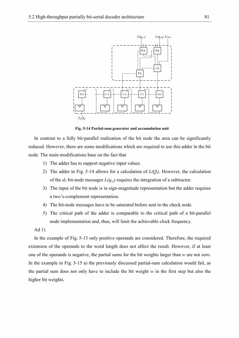
5.2 High-throughput partially bit-serial decoder architecture 81
Fig. 5-14 Partial-sum generator and accumulation unit
In contrast to a fully bit-parallel realization of the bit node the area can be significantly
reduced. However, there are some modifications which are required to use this adder in the bit
node. The main modifications base on the fact that
1) The adder has to support negative input values.
2) The adder in Fig. 5-14 allows for a calculation of L(Qi). However, the calculation
of the dV bit-node messages L(qi,j) requires the integration of a subtractor.
3) The input of the bit node is in sign-magnitude representation but the adder requires
a two’s-complement representation.
4) The bit-node messages have to be saturated before sent to the check node.
5) The critical path of the adder is comparable to the critical path of a bit-parallel
node implementation and, thus, will limit the achievable clock frequency.
Ad 1)
In the example of Fig. 5-13 only positive operands are considered. Therefore, the required
extension of the operands to the word length does not affect the result. However, if at least
one of the operands is negative, the partial sums for the bit weights larger than w are not zero.
In the example in Fig. 5-15 a) the previously discussed partial-sum calculation would fail, as
the partial sum does not only have to include the bit weight w in the first step but also the
higher bit weights.
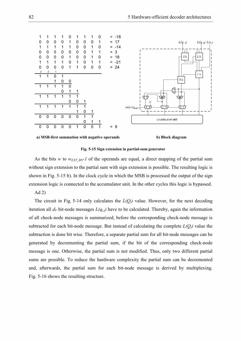
82 5 Hardware-efficient decoder architectures
1 1 1 1 0 1 1 1 0 = -18
0 0 0 0 1 0 0 0 1 = 17
1 1 1 1 1 0 0 1 0 = -14
0 0 0 0 0 0 0 1 1 = 3
0 0 0 0 1 0 0 1 0 = 18
1 1 1 1 0 1 0 1 1 = -21
0 0 0 0 1 1 0 0 0 = 242 2 1
1 1 0 1
1 0 0
1 1 1 1 0
0 1 1
1 1 1 1 1 1
0 0 1
1 1 1 1 1 1 1
1 0 1
0 0 0 0 0 0 1 1
0 1 1
0 0 0 0 0 1 0 0 1 = 9
a) MSB-first summation with negative operands b) Block diagram
Fig. 5-15 Sign extension in partial-sum generator
As the bits w to wEXT_BN-1 of the operands are equal, a direct mapping of the partial sum
without sign extension to the partial sum with sign extension is possible. The resulting logic is
shown in Fig. 5-15 b). In the clock cycle in which the MSB is processed the output of the sign
extension logic is connected to the accumulator unit. In the other cycles this logic is bypassed.
Ad 2)
The circuit in Fig. 5-14 only calculates the L(Qi) value. However, for the next decoding
iteration all dV bit-node messages L(qi,j) have to be calculated. Thereby, again the information
of all check-node messages is summarized, before the corresponding check-node message is
subtracted for each bit-node message. But instead of calculating the complete L(Qi) value the
subtraction is done bit wise. Therefore, a separate partial sum for all bit-node messages can be
generated by decrementing the partial sum, if the bit of the corresponding check-node
message is one. Otherwise, the partial sum is not modified. Thus, only two different partial
sums are possible. To reduce the hardware complexity the partial sum can be decremented
and, afterwards, the partial sum for each bit-node message is derived by multiplexing.
Fig. 5-16 shows the resulting structure.
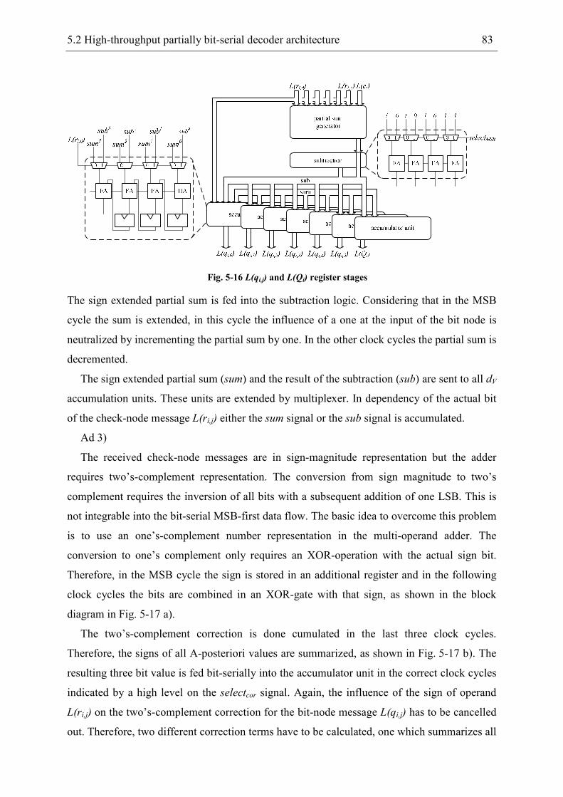
5.2 High-throughput partially bit-serial decoder architecture 83
Fig. 5-16 L(qi,j) and L(Qi) register stages
The sign extended partial sum is fed into the subtraction logic. Considering that in the MSB
cycle the sum is extended, in this cycle the influence of a one at the input of the bit node is
neutralized by incrementing the partial sum by one. In the other clock cycles the partial sum is
decremented.
The sign extended partial sum (sum) and the result of the subtraction (sub) are sent to all dV
accumulation units. These units are extended by multiplexer. In dependency of the actual bit
of the check-node message L(ri,j) either the sum signal or the sub signal is accumulated.
Ad 3)
The received check-node messages are in sign-magnitude representation but the adder
requires two’s-complement representation. The conversion from sign magnitude to two’s
complement requires the inversion of all bits with a subsequent addition of one LSB. This is
not integrable into the bit-serial MSB-first data flow. The basic idea to overcome this problem
is to use an one’s-complement number representation in the multi-operand adder. The
conversion to one’s complement only requires an XOR-operation with the actual sign bit.
Therefore, in the MSB cycle the sign is stored in an additional register and in the following
clock cycles the bits are combined in an XOR-gate with that sign, as shown in the block
diagram in Fig. 5-17 a).
The two’s-complement correction is done cumulated in the last three clock cycles.
Therefore, the signs of all A-posteriori values are summarized, as shown in Fig. 5-17 b). The
resulting three bit value is fed bit-serially into the accumulator unit in the correct clock cycles
indicated by a high level on the selectcor signal. Again, the influence of the sign of operand
L(ri,j) on the two’s-complement correction for the bit-node message L(qi,j) has to be cancelled
out. Therefore, two different correction terms have to be calculated, one which summarizes all
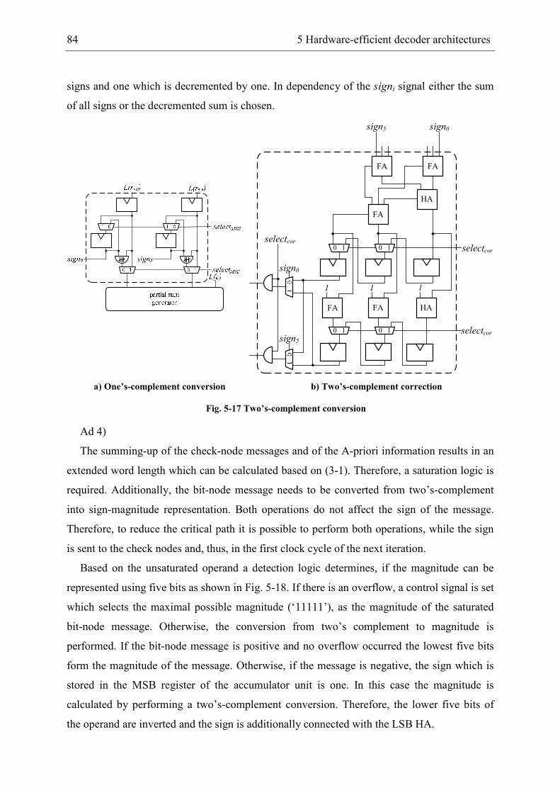
84 5 Hardware-efficient decoder architectures
signs and one which is decremented by one. In dependency of the signi signal either the sum
of all signs or the decremented sum is chosen.
FA FA
sign5 sign0
HA
FA
0 10 1
FAFA HA
1 11
0 10 1 selectcor
selectcorselectcor
sign0
sign5
a) One’s-complement conversion b) Two’s-complement correction
Fig. 5-17 Two’s-complement conversion
Ad 4)
The summing-up of the check-node messages and of the A-priori information results in an
extended word length which can be calculated based on (3-1). Therefore, a saturation logic is
required. Additionally, the bit-node message needs to be converted from two’s-complement
into sign-magnitude representation. Both operations do not affect the sign of the message.
Therefore, to reduce the critical path it is possible to perform both operations, while the sign
is sent to the check nodes and, thus, in the first clock cycle of the next iteration.
Based on the unsaturated operand a detection logic determines, if the magnitude can be
represented using five bits as shown in Fig. 5-18. If there is an overflow, a control signal is set
which selects the maximal possible magnitude (‘11111’), as the magnitude of the saturated
bit-node message. Otherwise, the conversion from two’s complement to magnitude is
performed. If the bit-node message is positive and no overflow occurred the lowest five bits
form the magnitude of the message. Otherwise, if the message is negative, the sign which is
stored in the MSB register of the accumulator unit is one. In this case the magnitude is
calculated by performing a two’s-complement conversion. Therefore, the lower five bits of
the operand are inverted and the sign is additionally connected with the LSB HA.
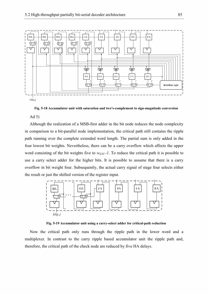
5.2 High-throughput partially bit-serial decoder architecture 85
Fig. 5-18 Accumulator unit with saturation and two’s-complement to sign-magnitude conversion
Ad 5)
Although the realization of a MSB-first adder in the bit node reduces the node complexity
in comparison to a bit-parallel node implementation, the critical path still contains the ripple
path running over the complete extended word length. The partial sum is only added in the
four lowest bit weights. Nevertheless, there can be a carry overflow which affects the upper
word consisting of the bit weights five to wEXT -1. To reduce the critical path it is possible to
use a carry select adder for the higher bits. It is possible to assume that there is a carry
overflow in bit weight four. Subsequently, the actual carry signal of stage four selects either
the result or just the shifted version of the register input.
Fig. 5-19 Accumulator unit using a carry-select adder for critical-path reduction
Now the critical path only runs through the ripple path in the lower word and a
multiplexer. In contrast to the carry ripple based accumulator unit the ripple path and,
therefore, the critical path of the check node are reduced by five HA delays.
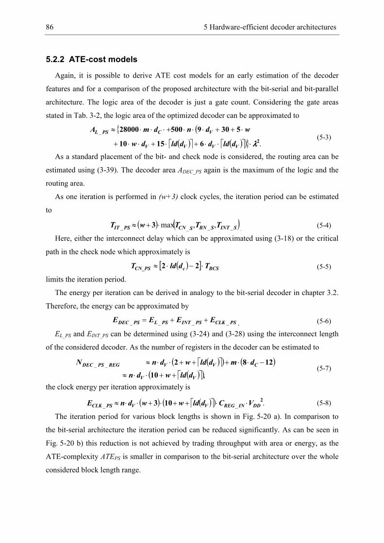
86 5 Hardware-efficient decoder architectures
5.2.2 ATE-cost models
Again, it is possible to derive ATE cost models for an early estimation of the decoder
features and for a comparison of the proposed architecture with the bit-serial and bit-parallel
architecture. The logic area of the decoder is just a gate count. Considering the gate areas
stated in Tab. 3-2, the logic area of the optimized decoder can be approximated to
{ (( ) ( ) )} .
_
261510
530950028000
λλλλ⋅⋅⋅+⋅+⋅⋅+
⋅++⋅⋅⋅+⋅⋅⋅≈
VVVV
VCPSL
dldddlddw
wdndmA
(5-3)
As a standard placement of the bit- and check node is considered, the routing area can be
estimated using (3-39). The decoder area ADEC_PS again is the maximum of the logic and the
routing area.
As one iteration is performed in (w+3) clock cycles, the iteration period can be estimated
to
( ) ( )SINTSBNSCNPSIT TTTwT ____ ,,max⋅+≈ 3.
(5-4)
Here, either the interconnect delay which can be approximated using (3-18) or the critical
path in the check node which approximately is
( )[ ] BCScCN_PS TdldT ⋅−⋅≈ 22
(5-5)
limits the iteration period.
The energy per iteration can be derived in analogy to the bit-serial decoder in chapter 3.2.
Therefore, the energy can be approximated by
PSCLKPSINTPSLPSDEC EEEE ____ ++=. (5-6)
EL_PS and EINT_PS can be determined using (3-24) and (3-28) using the interconnect length
of the considered decoder. As the number of registers in the decoder can be estimated to
( ) ( ) ( )( ) ( ),
__
VV
CVVREGPSDEC
dldwdn
dmdldwdnN
++⋅⋅≈
−⋅⋅+++⋅⋅≈
10
1282
(5-7)
the clock energy per iteration approximately is
( ) ( ) ( ) .__2
103 DDINREGVVPSCLK VCdldwwdnE ⋅⋅++⋅+⋅⋅≈
(5-8)
The iteration period for various block lengths is shown in Fig. 5-20 a). In comparison to
the bit-serial architecture the iteration period can be reduced significantly. As can be seen in
Fig. 5-20 b) this reduction is not achieved by trading throughput with area or energy, as the
ATE-complexity ATEPS is smaller in comparison to the bit-serial architecture over the whole
considered block length range.
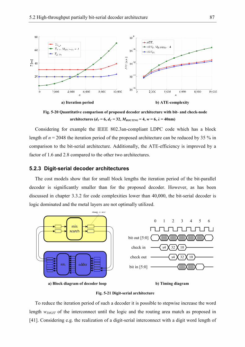
5.2 High-throughput partially bit-serial decoder architecture 87
a) Iteration period b) ATE-complexity
Fig. 5-20 Quantitative comparison of proposed decoder architecture with bit- and check-node
architectures (dV = 6, dC = 32, MROUTING = 4, w = 6, λ = 40nm)
Considering for example the IEEE 802.3an-compliant LDPC code which has a block
length of n = 2048 the iteration period of the proposed architecture can be reduced by 35 % in
comparison to the bit-serial architecture. Additionally, the ATE-efficiency is improved by a
factor of 1.6 and 2.8 compared to the other two architectures.
5.2.3 Digit-serial decoder architectures
The cost models show that for small block lengths the iteration period of the bit-parallel
decoder is significantly smaller than for the proposed decoder. However, as has been
discussed in chapter 3.3.2 for code complexities lower than 40,000, the bit-serial decoder is
logic dominated and the metal layers are not optimally utilized.
4 5 60 1 2 3
bit out [5:0]
check in
check out
bit in [5:0]
s4 32 10
s4 32 10
a) Block diagram of decoder loop b) Timing diagram
Fig. 5-21 Digit-serial architecture
To reduce the iteration period of such a decoder it is possible to stepwise increase the word
length wDIGIT of the interconnect until the logic and the routing area match as proposed in
[41]. Considering e.g. the realization of a digit-serial interconnect with a digit word length of
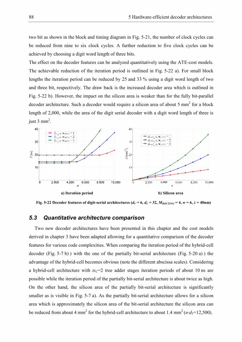
88 5 Hardware-efficient decoder architectures
two bit as shown in the block and timing diagram in Fig. 5-21, the number of clock cycles can
be reduced from nine to six clock cycles. A further reduction to five clock cycles can be
achieved by choosing a digit word length of three bits.
The effect on the decoder features can be analyzed quantitatively using the ATE-cost models.
The achievable reduction of the iteration period is outlined in Fig. 5-22 a). For small block
lengths the iteration period can be reduced by 25 and 33 % using a digit word length of two
and three bit, respectively. The draw back is the increased decoder area which is outlined in
Fig. 5-22 b). However, the impact on the silicon area is weaker than for the fully bit-parallel
decoder architecture. Such a decoder would require a silicon area of about 5 mm2 for a block
length of 2,000, while the area of the digit serial decoder with a digit word length of three is
just 3 mm2.
T[ns]
A[mm2]
a) Iteration period b) Silicon area
Fig. 5-22 Decoder features of digit-serial architectures (dV = 6, dC = 32, MROUTING = 4, w = 6, λ = 40nm)
5.3 Quantitative architecture comparison
Two new decoder architectures have been presented in this chapter and the cost models
derived in chapter 3 have been adapted allowing for a quantitative comparison of the decoder
features for various code complexities. When comparing the iteration period of the hybrid-cell
decoder (Fig. 5-7 b) ) with the one of the partially bit-serial architecture (Fig. 5-20 a) ) the
advantage of the hybrid-cell becomes obvious (note the different abscissa scales). Considering
a hybrid-cell architecture with tsC=2 tree adder stages iteration periods of about 10 ns are
possible while the iteration period of the partially bit-serial architecture is about twice as high.
On the other hand, the silicon area of the partially bit-serial architecture is significantly
smaller as is visible in Fig. 5-7 a). As the partially bit-serial architecture allows for a silicon
area which is approximately the silicon area of the bit-serial architecture the silicon area can
be reduced from about 4 mm2 for the hybrid-cell architecture to about 1.4 mm
2 (n·dV=12,500).
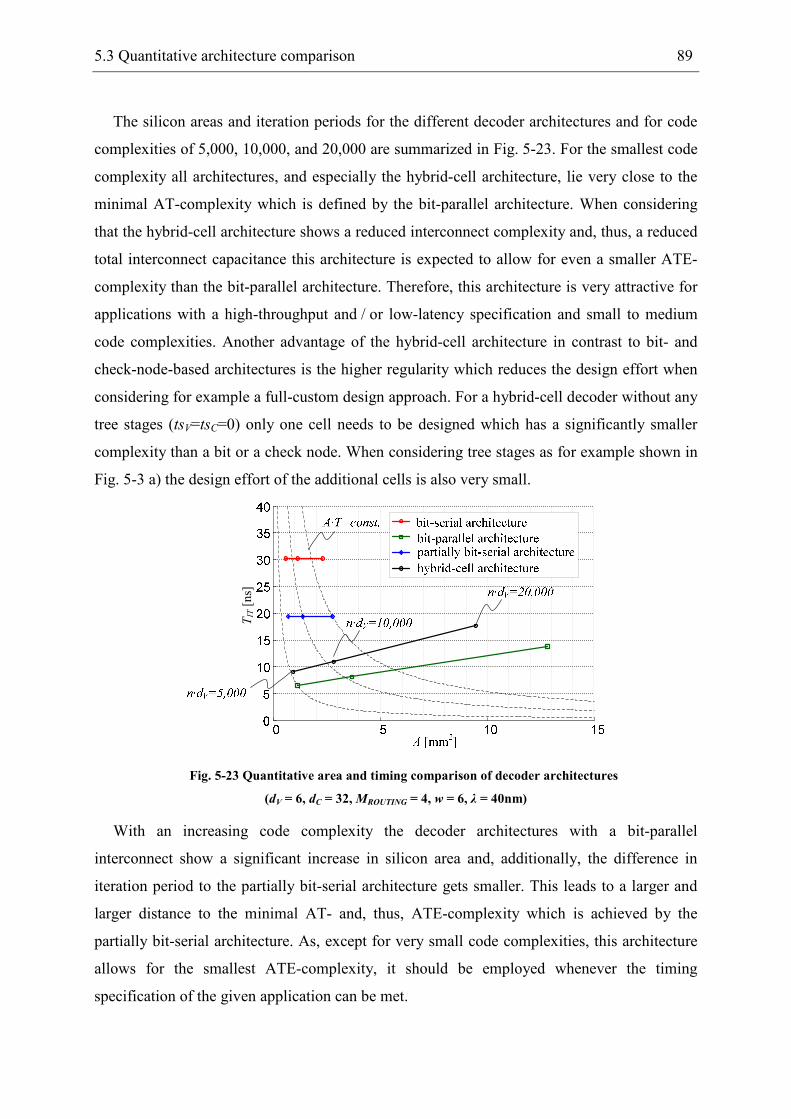
5.3 Quantitative architecture comparison 89
The silicon areas and iteration periods for the different decoder architectures and for code
complexities of 5,000, 10,000, and 20,000 are summarized in Fig. 5-23. For the smallest code
complexity all architectures, and especially the hybrid-cell architecture, lie very close to the
minimal AT-complexity which is defined by the bit-parallel architecture. When considering
that the hybrid-cell architecture shows a reduced interconnect complexity and, thus, a reduced
total interconnect capacitance this architecture is expected to allow for even a smaller ATE-
complexity than the bit-parallel architecture. Therefore, this architecture is very attractive for
applications with a high-throughput and / or low-latency specification and small to medium
code complexities. Another advantage of the hybrid-cell architecture in contrast to bit- and
check-node-based architectures is the higher regularity which reduces the design effort when
considering for example a full-custom design approach. For a hybrid-cell decoder without any
tree stages (tsV=tsC=0) only one cell needs to be designed which has a significantly smaller
complexity than a bit or a check node. When considering tree stages as for example shown in
Fig. 5-3 a) the design effort of the additional cells is also very small.
TIT [ns]
Fig. 5-23 Quantitative area and timing comparison of decoder architectures
(dV = 6, dC = 32, MROUTING = 4, w = 6, λ = 40nm)
With an increasing code complexity the decoder architectures with a bit-parallel
interconnect show a significant increase in silicon area and, additionally, the difference in
iteration period to the partially bit-serial architecture gets smaller. This leads to a larger and
larger distance to the minimal AT- and, thus, ATE-complexity which is achieved by the
partially bit-serial architecture. As, except for very small code complexities, this architecture
allows for the smallest ATE-complexity, it should be employed whenever the timing
specification of the given application can be met.

6 Highly-optimized full-custom designed LDPC decoder
The optimization of high-throughput LDPC decoders started on algorithm and architecture
level is continued on circuit and physical implementation level in the following. Therefore, a
decoder macro has been further optimized and realized in a 40-nm CMOS technology [57].
As currently the IEEE 802.3 an [6] is the most challenging standard from a throughput
perspective it has been chosen as the exemplary code. It has been shown, that for the code
complexity of 12,288 the new partially bit-serial decoder architecture features the smallest
decoder complexity (Fig. 5-20 and Fig. 5-23). Additionally, the hardware-efficient post-
processing factor identified in chapter 4.2.4 needs to be integrated into this architecture. To
continue the optimization on circuit and physical level the decoder is realized in a full-custom
design approach. Thereby, the high modularity of the LDPC decoder reduces the design
effort, while such a flow allows for an extensive optimization on lower design levels.
6.1 Decoder implementation
In chapter 4 it is shown that the Min-Sum algorithm in combination with a normalization
factor of 0.5 allows for almost the optimal decoding performance and simultaneously reduces
the hardware complexity. In the proposed decoder architecture the main advantage is the
reduced iteration period. In contrast to the decoder in Fig. 5-9 c) the iteration period can be
reduced from w+3 to only w+2 clock cycles as the timing diagrams in Fig. 6-1 reveal.
8 94 5 6 70 1 2 3
bit out [5:0]
0
check in
check out
bit in [5:0]
1 0
s 4 3 2 1
s 4 3 2
0
s 3 2 1check in
check out
bit in [4:0]
0
s 3 2 1
bit out [4:0]
0 1 2 3 84 5 6 7
a) Without post-processing function b) With hardware-efficient normalization factor
Fig. 6-1 Timing diagram of optimized architecture
The check node is not affected by the introduction of the hardware-efficient normalization
factor. Therefore, both check-node architectures described in chapter 5.2 can be used. As
there is nearly no difference in silicon area and critical path, the minimum search of Fig. 5-11
is chosen in the following. A schematic of the check node including the input and output
registers and the sign calculation is shown in Fig. 6-2. In the schematic the used partitioning
of the check node to allow for a full-custom design scheme is illustrated, additionally. The
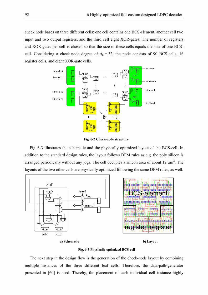
92 6 Highly-optimized full-custom designed LDPC decoder
check node bases on three different cells: one cell contains one BCS-element, another cell two
input and two output registers, and the third cell eight XOR-gates. The number of registers
and XOR-gates per cell is chosen so that the size of these cells equals the size of one BCS-
cell. Considering a check-node degree of dC = 32, the node consists of 90 BCS-cells, 16
register cells, and eight XOR-gate cells.
Fig. 6-2 Check-node structure
Fig. 6-3 illustrates the schematic and the physically optimized layout of the BCS-cell. In
addition to the standard design rules, the layout follows DFM rules as e.g. the poly silicon is
arranged periodically without any jogs. The cell occupies a silicon area of about 12 µm2. The
layouts of the two other cells are physically optimized following the same DFM rules, as well.
111111111
111111111111
111111
111111111111111111111
111111
111111111111111111111
11111111111111
1111111111111111111111111111
1111
11111111111111111111111111111111111111
11111111111111111111111
111111111
111111111111111111111111111
11111111
11
111111111
11
111111111111111111111111111111111111111
111111111111
111111111111111111111111
1111111111
1111111111111111
111111111111111111111111111111111111
111111111111111111
11111111111111111111111111111111111111
111111111111
1111111111111111111111111111111111
11111111111111
111111111111111111111
11111111
111111
111111111111111111111111111111
111111111111111111111
111111111111111111111111
111111111111111
111111111111
1111111111111111
111111111111111111111111
111111111
11111111
111111111111111
111111111111111111111111111111
111111
111111111111
11111111
111111111111111
11111111
111111111111111
111111111111111111111111111111111111111111111111111111111111111
111111111111111111111111
111111111
11111111111111111111111111111111111111111111
11111111111111111111111111111111
111111
11111111111111111111
11111111111111111111
11111111111111111111111111111 111
111111111111111111111111111111
111111111111111111111111
111111111111111111
111111111
111111111111111111111111
111111111111111
111111111111111111
111111111111111
1111111111111111
111111111111111
111111111111
111111111111111111
111111111111111111111111111111
11111111111111111111
11111111111111111111
111111111111111111111111111111
111111
11111111111111111111
1111111111111111
111111
111111111111111
111111
111111111111111111
11111111111111 111
111111111
11111111111111
11111111
11111111111111111111
11111111111111111111111111
111111111111
11111111111111
1111111111
111111111111111111
11111111
11111111111111
11111111111111
111111111111111111111111111111111111111111111
11111111111111111111
111111111111111111111111111
11111111111111
111111111111
111111111111111111
11111111111111111111
111111111111111111111
111111
111111111111
1111111111
111111111
11111111
111111111111
11111111111111111111
11111111111111111111
111111111111111111111111111111111111111111111111111111111111111111111111111111111111111111
111111111111
111111111111111111
1111111111111111
111111111111111111111111111111111111111111
111111111111
11111111
111111111
11111111111111
11111111111111
111111111111111111
111111
11111111111111
1111111111
111111111111111
1111111111111111111111111111
111111111111111111
111111
1111111
1111111111
111111111111111
1111111111111111
111111111111
111111111
111111111111111
1111111111111111
111111111111111111111111111111
111111111111
111111111111111
11111111
11111111111111
111111111111
111111111111111111111111111111111
11111111111111111111
1111111111111111
111111111
11111111
111111
1111111111111111111111111111111111111111111111111111111111111111111111
111111111
11111111111111111111
111111
11111111111111
11111111111111111111
111111111111
111111111111111111111
1111
111111111111111111111
111111111111111111111111111111111111
111111111111111111111111
111111
11111111111111111111111111111111111111111111111111
111111
11111111
111111
1111111111111111
111111111111111111111111111
1111111111111111111111111111111111111111
111111111
111111111111111
11111111111111111111
111111111111111
111111111111111111111
11111111111111111111
111111111111111111111
111111111111111
1111111111111111111111
11111111111111111111
111111111111
11111111111111111111111111111111
111111111111111111111111
1111111111
11111111111111111111111111111111
111111111111111
111111111111111111
1111111111111111
111111111111111111111111
11111111111111111111111111111111111111111111111111111111
11111111111111 1111
111111111111
111111
1111111111111111
111111 11111
1111111111
111111
111111
111111111111111111111111111111111111111
1111
111111111111111111111111111111
111111111111111111111111111111111111111111
111111111111111111111111111111
11111111111111111111111111111111111111111111111111111111
111111111111111111111111111111
1111111111111111111111111111111111111111
111111111111111111111111111111
1111111111111111111111111111111111111111
111111111111111111
111111111111111111111111111111111111111111111111111111111111
111111111111111111111111111111111111111111111111
1111111111111111111111111111111111111111
1111111111111111111111111111111111111111
111111111111111111111111111111111111
111111111111111111111111111111111111111111111111111111111111111111111111111111111111111111111111111111111111111111
11111111111111111111111111111111111111111111111111111111111111111111111111111111111111111111111111111111111111111111111111111111111111111111111111111111111111111111111111111111111111111111111111111111111111111111
1111111111111111111111111111111111111111111111111111111111111111
111111111111111111111111111111
11111111111111111111111111111111111111111111111111111111111111111111
1111111111111111111111111111111111111111
1111111111111111111111111111111111111111111111111111
111111111111111111111111111
1111111111111111111111111111111111111111111111111111111111111111
1111111111111111111111111111111111111111111111111111
111111111111111111111111111111111111111111111111111
111111111111111111111111111111
111111111111111111111111111111
1111111111111111111111111111111111111111
111111111111111111
111111111111111111111111111111111111111111111111
111111111111111111111
111111111111111111111111111111111111111111111111111111111111111
111111111111111111111111111111111111111111111111
111111111111111111111111111111111111111111111111111111111111111111111111111111111111
1111111111111111111111111111111111111111111111111111111111111111111111111111111111111
1111111111111111111111111111111111111111111111111111111111111111111111111111111111111
11111111111111111111111111111111111111111111
111111111111111111111111111111111111111111111111111111111111111111111111111111111111111111111111111111111111111111111111111111111111111111111111111111111111111111111111111111111111111111111111111111111111111111111111111111111
1111111111111111111111111111111111111111111111111111111111111111111111
1111111111111111111111111111111111
111111111111111111111111111111111111111111111111111111111111111111111111111111111111111
111111111111111111111111111111111111111111
111111111111111111111111111111111111111111111111111111
111111111111111111111111111111111111111111111111111111111111111111111111111111111111111111111111111111111111111111111111111111111111111111111111111111111111111111111111111111111111111111111111111111111111111111111111111111111
111111111111111111111111111111111111111111111111
111111111111111111111111111111111111111111111111111111111111111111111111111111111111111111111111111111111111111111111111111111111111111111111111111111111111111111111111111111111111111111111111111111111111111111111111111111111111
111111111111111111111111111111111111111111111111111111111111111111111111111111111111111111111111111111111111111111111111111111111111111111111111111111111111111111111111111111111111111111111111111111111111111111111111111111111
111111111111111111111111111111111111111111
111111111111111111111111111111111111111111111111111111111111111111111111111111111111111111111111111111111111111111111111111111111111111111111111111111111111111111111111111111111111111111111111111111111111111111111111111111111111
111111111111111111111111
1111111111111111111111
111111111111111111111111111111111111111111
111111111111111111111111
111111111111111111111111111111111
1111111111111111111111111111111111111111
111111111111111111111111111111
111111111111111111111111
111111111111111111111111111111111111111111111111111111111111
111111
111111111111111111111
111111111111111111111111
1111111111111111
111111111111111111
1111111111111111111111111111111111111111111111111111111111111111111111111111111111111111111111111111111111111111111111
1111111111111111111111
1111111111111111
111111111111111111
111111111111111111111111111111111111111111111111111111111111111111111111111111111111111111111111111111
111111111111111111111111111111111111111111111111111111111111111111111111111111111111111111111111111111111111111111111111111111111111111111111111111111
11111111111111111111111111111111
111111111111111111
1111111111111111
111111111111111111111111111111111111111111111111111111111111111111111111111111111111111111111111111111111111111111111111111111111111111111111111111111
111111111111111111111111111111111111111111111111111111111111111111111111111111111111111111111111111111111111111111111111111111111111
1111111111111111111111111111111111111111111111
111111111111111111111111111111111111111111111111111111111111111111111111111111111111111111111111111111111111111111111111111111111111111111111111111111111111111111111111111111111111111111111111111111111111111111111111111111111
111111111111111111111111111111111111111111111111111111111111111111111111111111111111111111111111111111111111111111111111111111111111111111111111111111111111111111111111111111111111111111111111111111111111111111111111111111111
11111111111111111111
11111111111111111111
111111111111111111
1111111111111111
11111111111111111111111111
111111111111111111
111111111111111111
111111111111111111
111111111111111111
1111111111111111111111111111
111111111111111111111111111111111111111111111111111111111111111111111111111111111111111111111111111111111111111111111111111111111111111111111111111111
11111111111111111111111111111111111111111111111111111111111111111111111111
11111111111111111111111111111111
111111111111111111111111111111111111111111111111111111111111111111111111111111111111111111111111111111111111111111111111111111111111111111111111111111
1111111111111111111111111111
1111111111111111
111111111111111111111111111111111111111111111111111111111111111111111111111111111111111111111111111111111111111111111111111111111111111111111111111111111111111111111111111111111111111111111111111111111111111111111111111111111
111111111111111111111111111111111111111111111111111111111111111111111111111111111111111111111111111111111111111111111111111111111111111111111111111111111111111111111111111111111111111111111111
111111111111111111111111111111111111111111111111111111111111111111111111111111111111111111111111111111111111111111111111111111111111111111111111111111111111111111111111111111111111111111111111111111111111111111111111111111111
11111111111111
11111111111111111111
1111111111111111111111111111
11111111111111111111111111
1111111111111111111111111111111111111111
1111111111111111111111111111111111111111111111111111111111111111111111111111111111111111111111111111111111111111111111
111111111111111111
111111111111111111111111111111111111111111111111111111111111111111111111111111111111111111111111111111111111111111111111111111111111111111111111111111111111111111
11111111111111111111111111111111111111111111111111111111111111111111111111111111111111
111111111111111111111111111111
111111111111111111111111111
11111111111111111111111111111111111111111111111111111111111111111111111111111111111111
111111111111111111111111111111111111111111111111111111
1111111111111111111111111111
111111111111111111111111111111111111111111111111111111111111
111111111111111111111111111111
1111111111111111111111111111
1111111111111111111111111111
111111111111111111111111111111111111
111111111111111111
111111111111111111111111111111111111
11111111111111111111111111
111111111111111111111111111111111111111111111
111111111111111111111111
1111111111111111111111111111
11111111111111111111111111111111111111111111111111111111111111111111111111111111111111111111
1111111111111111111111111111
1111111111111111111111111111
111111111111111111111111111111111111
111111111111111111111111
1111111111111111
111111111111
1111111111111111
111111
1111111111111111111111111111111111111111111111111111111111111111111111111111111111111111111111111111111111111111111111111111
1111111111111111111111111111111111
111111111111111111111111111111
11111111111111111111111111111111111111111111111111111111111111
11111111111111111111111111111111111111111111111111111111111111111111
11111111111111111111111111111111111111111111111111111111
111111111111111111
111111111111111111
11111111111111111111111111111111111111111111111111111111111111
111111111111111111111111111111
111111111111111111
111111111
111111111111111111111111111111
111111111111111
111111111111111111111111111111
111111111111111111111111111111
1111111111111111111111111111111111111111111111111111111111
1111111111111111111111111111111111
11111111111111111111111111111111111111111111111111111111111111
11111111111111111111111111111111111111111111111111111111111111
111111111111111
111111111111111111111111111111
1111111111111111111111111111
1111111111111111111111111111
11111111111111
1111111111111111111111111111
111111111111111
111111111111111111111111111111
11111111111111111111111111111111111111111111111111111111111111111111111111111111111111111111
111111111111111111111111111111
11111111111111111111111111111111
111111111111111111111111111111111
11111111111111111111111111111
1111111111111111111111111111
111111111111111111111111111111111
11111111111111111111111111111111
11111111111111111111111111111111111111111111111111111111111111
111111111111111111111111
1111111111111111111111111111
1111111111111111111111
111111111111111111111111111111111111
111111111111111111111111111111111111111111111111111111111111
111111111111111111111111111111111111
1111111111111
a) Schematic b) Layout
Fig. 6-3 Physically optimized BCS-cell
The next step in the design flow is the generation of the check-node layout by combining
multiple instances of the three different leaf cells. Therefore, the data-path-generator
presented in [60] is used. Thereby, the placement of each individual cell instance highly
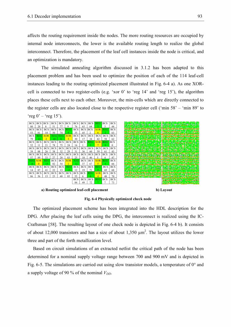
6.1 Decoder implementation 93
affects the routing requirement inside the nodes. The more routing resources are occupied by
internal node interconnects, the lower is the available routing length to realize the global
interconnect. Therefore, the placement of the leaf cell instances inside the node is critical, and
an optimization is mandatory.
The simulated annealing algorithm discussed in 3.1.2 has been adapted to this
placement problem and has been used to optimize the position of each of the 114 leaf-cell
instances leading to the routing optimized placement illustrated in Fig. 6-4 a). As one XOR-
cell is connected to two register-cells (e.g. ‘xor 0’ to ‘reg 14’ and ‘reg 15’), the algorithm
places these cells next to each other. Moreover, the min-cells which are directly connected to
the register cells are also located close to the respective register cell (‘min 58’ – ‘min 89’ to
‘reg 0’ – ‘reg 15’).
BCS
80
BCS
20
BCS
8
BCS
51
BCS
77
BCS
9
BCS
76
BCS
65
BCS
64
REG
3
BCS
3
BCS
44
BCS
53
BCS
81
BCS
10
BCS
50
BCS
74
REG
9
BCS
35
BCS
45
BCS
2
XOR
6
REG
2
BCS
63
BCS
79
REG
11
XOR
2
REG
10
REG
8
XOR
3
BCS
30
BCS
17
BCS
34
BCS
42
BCS
58
BCS
62
BCS
52
BCS
11
BCS
21
BCS
78
BCS
75
BCS
24
BCS
16
BCS
1
REG
1
XOR
7
REG
0
BCS
0
BCS
39
BCS
88
BCS
26
BCS
38
BCS
32
BCS
29
BCS
31
BCS
36
BCS
60
BCS
59
BCS
61
BCS
43BCS
57
BCS
89
BCS
33
BCS
27
BCS
28
BCS
83
BCS
25
BCS
18
BCS
46
BCS
5
BCS
4
BCS
47
REG
14
XOR
0
REG
15
BCS
82
BCS
54
XOR
1
REG
12
BCS
37
BCS
67
XOR
5
REG
4
BCS
66
BCS
14
BCS
87
BCS
41
BCS
22
BCS
13
REG
13
BCS
12
BCS
19
BCS
71
REG
5
BCS
69
BCS
68
BCS
86
BCS
56
BCS
15
BCS
23
BCS
40
BCS
85
BCS
55
BCS
6
REG
6
XOR
4
BCS
48
BCS
70
BCS
84
BCS
49
BCS
72
REG
7
BCS
7
BCS
73
a) Routing optimized leaf-cell placement b) Layout
Fig. 6-4 Physically optimized check node
The optimized placement scheme has been integrated into the HDL description for the
DPG. After placing the leaf cells using the DPG, the interconnect is realized using the IC-
Craftsman [58]. The resulting layout of one check node is depicted in Fig. 6-4 b). It consists
of about 12,000 transistors and has a size of about 1,350 µm2. The layout utilizes the lower
three and part of the forth metallization level.
Based on circuit simulations of an extracted netlist the critical path of the node has been
determined for a nominal supply voltage range between 700 and 900 mV and is depicted in
Fig. 6-5. The simulations are carried out using slow transistor models, a temperature of 0° and
a supply voltage of 90 % of the nominal VDD.
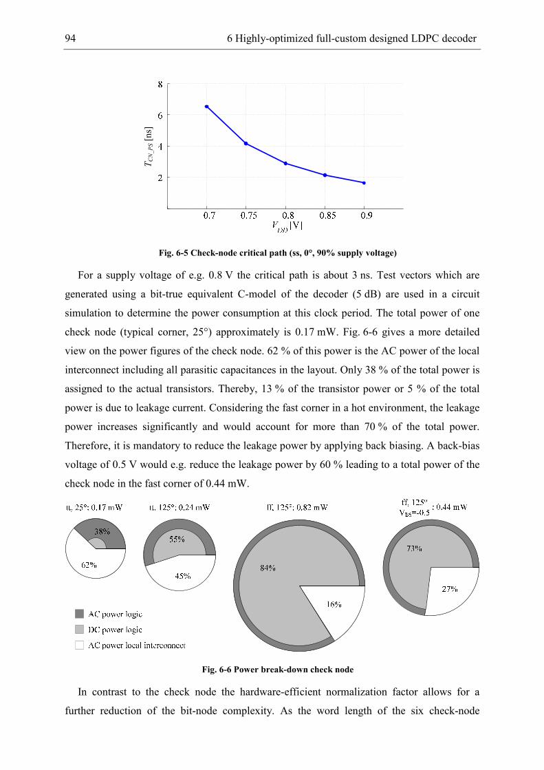
94 6 Highly-optimized full-custom designed LDPC decoder
TCN_PS[ns]
Fig. 6-5 Check-node critical path (ss, 0°, 90% supply voltage)
For a supply voltage of e.g. 0.8 V the critical path is about 3 ns. Test vectors which are
generated using a bit-true equivalent C-model of the decoder (5 dB) are used in a circuit
simulation to determine the power consumption at this clock period. The total power of one
check node (typical corner, 25°) approximately is 0.17 mW. Fig. 6-6 gives a more detailed
view on the power figures of the check node. 62 % of this power is the AC power of the local
interconnect including all parasitic capacitances in the layout. Only 38 % of the total power is
assigned to the actual transistors. Thereby, 13 % of the transistor power or 5 % of the total
power is due to leakage current. Considering the fast corner in a hot environment, the leakage
power increases significantly and would account for more than 70 % of the total power.
Therefore, it is mandatory to reduce the leakage power by applying back biasing. A back-bias
voltage of 0.5 V would e.g. reduce the leakage power by 60 % leading to a total power of the
check node in the fast corner of 0.44 mW.
Fig. 6-6 Power break-down check node
In contrast to the check node the hardware-efficient normalization factor allows for a
further reduction of the bit-node complexity. As the word length of the six check-node
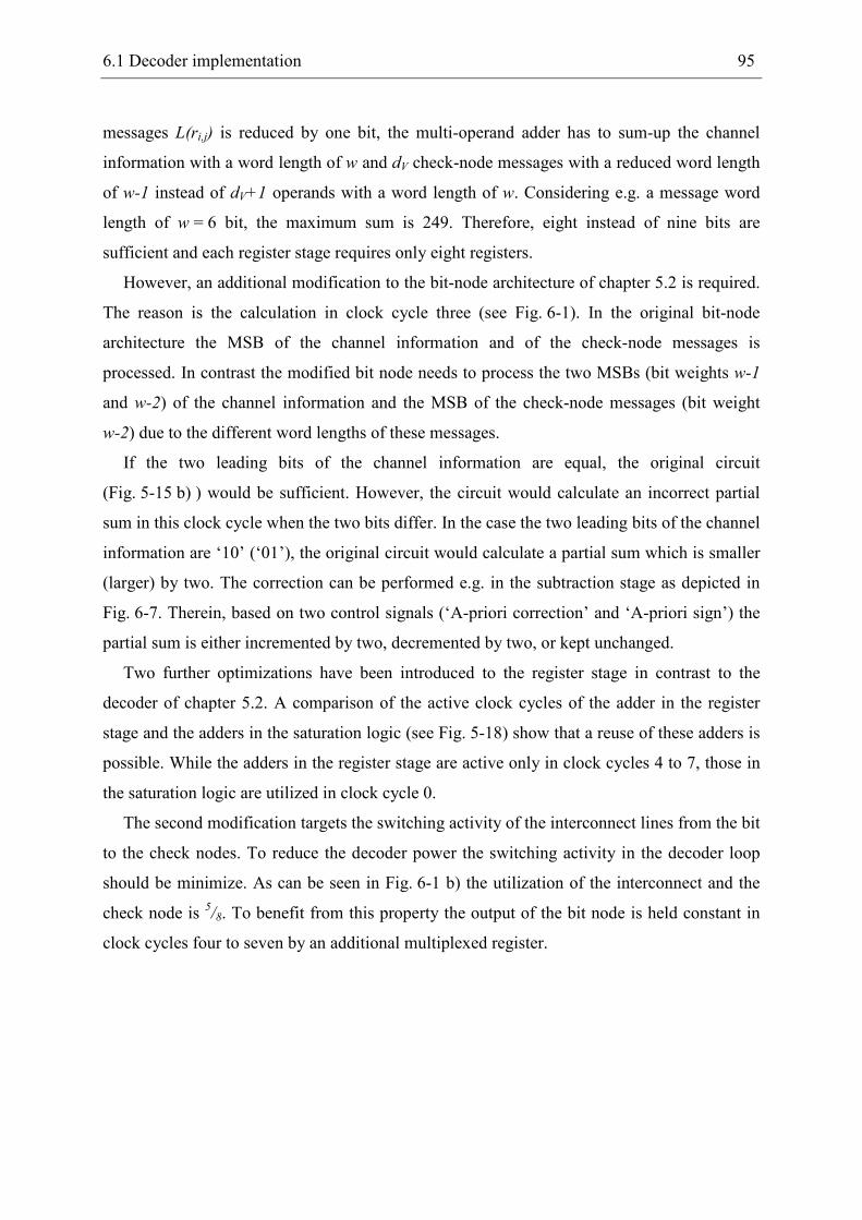
6.1 Decoder implementation 95
messages L(ri,j) is reduced by one bit, the multi-operand adder has to sum-up the channel
information with a word length of w and dV check-node messages with a reduced word length
of w-1 instead of dV+1 operands with a word length of w. Considering e.g. a message word
length of w = 6 bit, the maximum sum is 249. Therefore, eight instead of nine bits are
sufficient and each register stage requires only eight registers.
However, an additional modification to the bit-node architecture of chapter 5.2 is required.
The reason is the calculation in clock cycle three (see Fig. 6-1). In the original bit-node
architecture the MSB of the channel information and of the check-node messages is
processed. In contrast the modified bit node needs to process the two MSBs (bit weights w-1
and w-2) of the channel information and the MSB of the check-node messages (bit weight
w-2) due to the different word lengths of these messages.
If the two leading bits of the channel information are equal, the original circuit
(Fig. 5-15 b) ) would be sufficient. However, the circuit would calculate an incorrect partial
sum in this clock cycle when the two bits differ. In the case the two leading bits of the channel
information are ‘10’ (‘01’), the original circuit would calculate a partial sum which is smaller
(larger) by two. The correction can be performed e.g. in the subtraction stage as depicted in
Fig. 6-7. Therein, based on two control signals (‘A-priori correction’ and ‘A-priori sign’) the
partial sum is either incremented by two, decremented by two, or kept unchanged.
Two further optimizations have been introduced to the register stage in contrast to the
decoder of chapter 5.2. A comparison of the active clock cycles of the adder in the register
stage and the adders in the saturation logic (see Fig. 5-18) show that a reuse of these adders is
possible. While the adders in the register stage are active only in clock cycles 4 to 7, those in
the saturation logic are utilized in clock cycle 0.
The second modification targets the switching activity of the interconnect lines from the bit
to the check nodes. To reduce the decoder power the switching activity in the decoder loop
should be minimize. As can be seen in Fig. 6-1 b) the utilization of the interconnect and the
check node is 5/8. To benefit from this property the output of the bit node is held constant in
clock cycles four to seven by an additional multiplexed register.
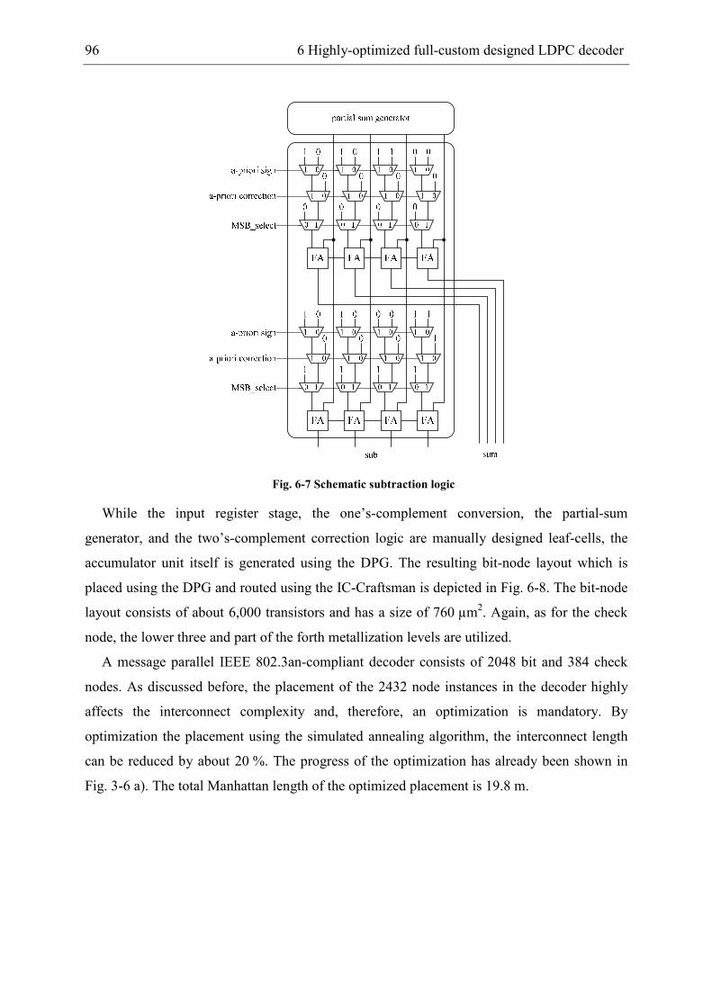
96 6 Highly-optimized full-custom designed LDPC decoder
Fig. 6-7 Schematic subtraction logic
While the input register stage, the one’s-complement conversion, the partial-sum
generator, and the two’s-complement correction logic are manually designed leaf-cells, the
accumulator unit itself is generated using the DPG. The resulting bit-node layout which is
placed using the DPG and routed using the IC-Craftsman is depicted in Fig. 6-8. The bit-node
layout consists of about 6,000 transistors and has a size of 760 µm2. Again, as for the check
node, the lower three and part of the forth metallization levels are utilized.
A message parallel IEEE 802.3an-compliant decoder consists of 2048 bit and 384 check
nodes. As discussed before, the placement of the 2432 node instances in the decoder highly
affects the interconnect complexity and, therefore, an optimization is mandatory. By
optimization the placement using the simulated annealing algorithm, the interconnect length
can be reduced by about 20 %. The progress of the optimization has already been shown in
Fig. 3-6 a). The total Manhattan length of the optimized placement is 19.8 m.
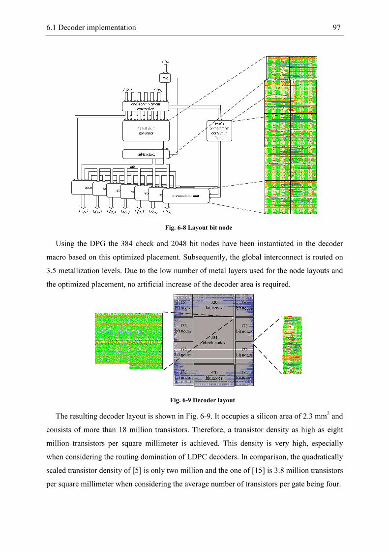
6.1 Decoder implementation 97
Fig. 6-8 Layout bit node
Using the DPG the 384 check and 2048 bit nodes have been instantiated in the decoder
macro based on this optimized placement. Subsequently, the global interconnect is routed on
3.5 metallization levels. Due to the low number of metal layers used for the node layouts and
the optimized placement, no artificial increase of the decoder area is required.
Fig. 6-9 Decoder layout
The resulting decoder layout is shown in Fig. 6-9. It occupies a silicon area of 2.3 mm2 and
consists of more than 18 million transistors. Therefore, a transistor density as high as eight
million transistors per square millimeter is achieved. This density is very high, especially
when considering the routing domination of LDPC decoders. In comparison, the quadratically
scaled transistor density of [5] is only two million and the one of [15] is 3.8 million transistors
per square millimeter when considering the average number of transistors per gate being four.
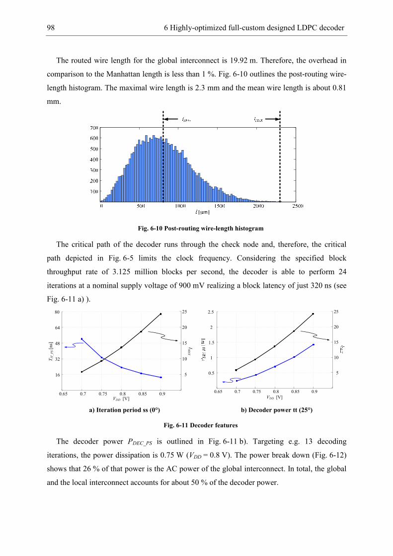
98 6 Highly-optimized full-custom designed LDPC decoder
The routed wire length for the global interconnect is 19.92 m. Therefore, the overhead in
comparison to the Manhattan length is less than 1 %. Fig. 6-10 outlines the post-routing wire-
length histogram. The maximal wire length is 2.3 mm and the mean wire length is about 0.81
mm.
Fig. 6-10 Post-routing wire-length histogram
The critical path of the decoder runs through the check node and, therefore, the critical
path depicted in Fig. 6-5 limits the clock frequency. Considering the specified block
throughput rate of 3.125 million blocks per second, the decoder is able to perform 24
iterations at a nominal supply voltage of 900 mV realizing a block latency of just 320 ns (see
Fig. 6-11 a) ).
0.65 0.7 0.75 0.8 0.85 0.9
16
32
48
64
80
VDD [V]
TIT_PS[ns]
5
10
15
20
25
IMAX
0.65 0.7 0.75 0.8 0.85 0.9
0.5
1
1.5
2
2.5
5
10
15
20
25
VDD [V]
a) Iteration period ss (0°) b) Decoder power tt (25°)
Fig. 6-11 Decoder features
The decoder power PDEC_PS is outlined in Fig. 6-11 b). Targeting e.g. 13 decoding
iterations, the power dissipation is 0.75 W (VDD = 0.8 V). The power break down (Fig. 6-12)
shows that 26 % of that power is the AC power of the global interconnect. In total, the global
and the local interconnect accounts for about 50 % of the decoder power.
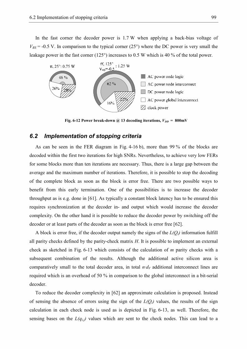
6.2 Implementation of stopping criteria 99
In the fast corner the decoder power is 1.7 W when applying a back-bias voltage of
VBS = -0.5 V. In comparison to the typical corner (25°) where the DC power is very small the
leakage power in the fast corner (125°) increases to 0.5 W which is 40 % of the total power.
Fig. 6-12 Power break-down @ 13 decoding iterations, VDD = 800mV
6.2 Implementation of stopping criteria
As can be seen in the FER diagram in Fig. 4-16 b), more than 99 % of the blocks are
decoded within the first two iterations for high SNRs. Nevertheless, to achieve very low FERs
for some blocks more than ten iterations are necessary. Thus, there is a large gap between the
average and the maximum number of iterations. Therefore, it is possible to stop the decoding
of the complete block as soon as the block is error free. There are two possible ways to
benefit from this early termination. One of the possibilities is to increase the decoder
throughput as is e.g. done in [61]. As typically a constant block latency has to be ensured this
requires synchronization at the decoder in- and output which would increase the decoder
complexity. On the other hand it is possible to reduce the decoder power by switching off the
decoder or at least parts of the decoder as soon as the block is error free [62].
A block is error free, if the decoder output namely the signs of the L(Qi) information fulfill
all parity checks defined by the parity-check matrix H. It is possible to implement an external
check as sketched in Fig. 6-13 which consists of the calculation of m parity checks with a
subsequent combination of the results. Although the additional active silicon area is
comparatively small to the total decoder area, in total n·dV additional interconnect lines are
required which is an overhead of 50 % in comparison to the global interconnect in a bit-serial
decoder.
To reduce the decoder complexity in [62] an approximate calculation is proposed. Instead
of sensing the absence of errors using the sign of the L(Qi) values, the results of the sign
calculation in each check node is used as is depicted in Fig. 6-13, as well. Therefore, the
sensing bases on the L(qi,j) values which are sent to the check nodes. This can lead to a
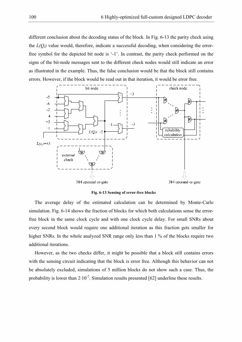
100 6 Highly-optimized full-custom designed LDPC decoder
different conclusion about the decoding status of the block. In Fig. 6-13 the parity check using
the L(Qi) value would, therefore, indicate a successful decoding, when considering the error-
free symbol for the depicted bit node is ‘-1’. In contrast, the parity check performed on the
signs of the bit-node messages sent to the different check nodes would still indicate an error
as illustrated in the example. Thus, the false conclusion would be that the block still contains
errors. However, if the block would be read out in that iteration, it would be error free.
Fig. 6-13 Sensing of error-free blocks
The average delay of the estimated calculation can be determined by Monte-Carlo
simulation. Fig. 6-14 shows the fraction of blocks for which both calculations sense the error-
free block in the same clock cycle and with one clock cycle delay. For small SNRs about
every second block would require one additional iteration as this fraction gets smaller for
higher SNRs. In the whole analyzed SNR range only less than 1 % of the blocks require two
additional iterations.
However, as the two checks differ, it might be possible that a block still contains errors
with the sensing circuit indicating that the block is error free. Although this behavior can not
be absolutely excluded, simulations of 5 million blocks do not show such a case. Thus, the
probability is lower than 2·10-7. Simulation results presented [62] underline these results.
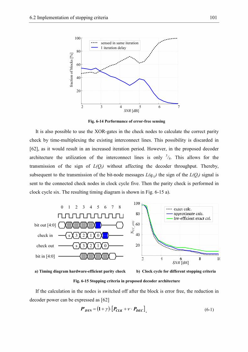
6.2 Implementation of stopping criteria 101
2 3 4 5 6 7
20
40
60
80
100
SNR [dB]
fraction of blocks [%]
sensed in same iteration
1 iteration delay
Fig. 6-14 Performance of error-free sensing
It is also possible to use the XOR-gates in the check nodes to calculate the correct parity
check by time-multiplexing the existing interconnect lines. This possibility is discarded in
[62], as it would result in an increased iteration period. However, in the proposed decoder
architecture the utilization of the interconnect lines is only 5/8. This allows for the
transmission of the sign of L(Qi) without affecting the decoder throughput. Thereby,
subsequent to the transmission of the bit-node messages L(qi,j) the sign of the L(Qi) signal is
sent to the connected check nodes in clock cycle five. Then the parity check is performed in
clock cycle six. The resulting timing diagram is shown in Fig. 6-15 a).
84 5 6 70 1 2 3
bit out [4:0]
check in
check out
bit in [4:0]
0
s 3 2 1 0
s 3 2 1
NCC_AVG
a) Timing diagram hardware-efficient parity check b) Clock cycle for different stopping criteria
Fig. 6-15 Stopping criteria in proposed decoder architecture
If the calculation in the nodes is switched off after the block is error free, the reduction in
decoder power can be expressed as [62]
( ) [ ]DECCLKDYN PPP ⋅+⋅+= νγ1'.
(6-1)
102 6 Highly-optimized full-custom designed LDPC decoder
ν is the fraction of the average number of clock cycles NCC_AVG in comparison to the
maximal number. γ is the power consumption overhead of the additional control logic which
typically can be neglected, as it will be done in the following. The activity factor can be
determined by Monte Carlo simulation. In Fig. 6-15 b) the resulting average number of clock
cycles for the decoder for the three different sensing schemes is outlined. The activity factor ν
can then be determined as
MAX
AVGCC
I8
N
⋅= _νννν .
(6-2)
As an external exact calculation of the stopping criteria results in the lowest number of
iterations and as it can be performed at the beginning of each iteration, it results in the lowest
average number of clock cycles (dashed line). In average the decoder is active between 21,
13.5, and 10 clock cycles for an SNRs of four, five, and six dB leading to an activity factor of
0.2, 0.13, and 0.1, respectively when considering a maximum of 13 decoding iterations.
For the approximate parity check the number of average active clock cycles is larger due to
possible additional iterations and due to the fact, that the calculation of the parity check is
performed with two clock cycles delay. For an SNR of five dB ν would be 0.17. Considering
the hardware-efficient exact sensing, the calculation is performed in clock cycle seven. In this
case ν would be 0.19.
In contrast to the decoder in [62] which requires interleaving to increase the decoding
throughput in the proposed decoder, the complete decoder macro can be shut down by clock
gating. Therefore, not only the dynamic power consumption of the nodes can be reduced by a
factor ν but also the clock power. The resulting decoder power can be estimated as
( ) [ ]DECCLKDYN PPP +⋅⋅+= νγ1''.
(6-3)
The power dissipation of the decoder for the three sensing schemes with node disabling
and clock gating is listed in Tab. 6-1. Thereby, 13 decoding iterations and a clock power of
28 % (Fig. 6-12) are assumed.
Starting from an energy per iteration of 16.3 nJ a disabling of the nodes would result in an
energy reduction of about 60 %. Thereby, the exact external calculation results in the largest
power reduction. However, as this would result in a significant hardware overhead the
implementation is not efficient. As the difference in power reduction between the three
sensing schemes is small, the hardware-efficient exact sensing scheme is favorable. Using this
scheme the hardware impact is minimized and a false indication of a faulty block as error free
is avoided. Although the clock fraction of the decoder power without early termination is only
28 %, in a decoder with node disabling this fraction is 67 %. Therefore, it is highly
6.3 Benchmarking 103
recommended to realize clock gating as in comparison to a decoder with just node disabling a
further power reduction of more than 50 % from 6.8 nJ to 3.3 nJ is possible.
Tab. 6-1 Early termination power reduction (typ, 25 °, SNR = 5dB, IMAX = 13)
Node disabling Node disabling + clk gating
EIT w/o early
termination EIT Reduction EIT Reduction
Exact sensing 16.3 nJ 6.0 nJ 63 % 2.1 nJ 87 %
Approx. sensing 16.3 nJ 6.5 nJ 60 % 2.7 nJ 83 %
HW-Efficient exact sensing 16.3 nJ 6.8 nJ 58 % 3.3 nJ 80 %
6.3 Benchmarking
Published decoder implementations are typically developed for different applications.
Therefore, a benchmarking of these implementations requires a fair scaling of the decoder
features. Even today nearly one decade after the publication of the first integrated LDPC
decoder it is still challenging to fairly compare decoders for different LDPC codes, as the
three basic metrics throughput, energy, and silicon area are highly complex functions of the
code parameters [63]. Therefore, it is customary to assume e.g. a linear scaling of the decoder
area with the block length n [62], [63]. Even worse is that the energy per bit and iteration is
typically assumed to be constant for various LDPC codes, as it is not scaled with respect to
code complexity. In contrast the ATE-cost models derived in chapter 3 e.g. show that for a
wide range of LDPC codes the silicon area scales quadratically with the block length leading
to a linear dependency between the energy per bit and the block length.
These models are used to derive fair scaling rules which are listed in Tab. 6-2. Thereby,
four types of decoders are distinguished:
A) Logic-dominated decoder with a bit-serial interconnect
B) Routing-dominated decoder with a bit-serial interconnect
C) Logic-dominated decoder with a bit-parallel interconnect
D) Routing-dominated decoder with a bit-parallel interconnect
Tab. 6-3 lists decoder implementations targeting a high decoder throughput and the code
and technology parameters which are required for the feature scaling. Furthermore, the
decoder features silicon area, iteration period, and energy per iteration are listed for the
individual code. As block interleaving and early termination to increase the decoder
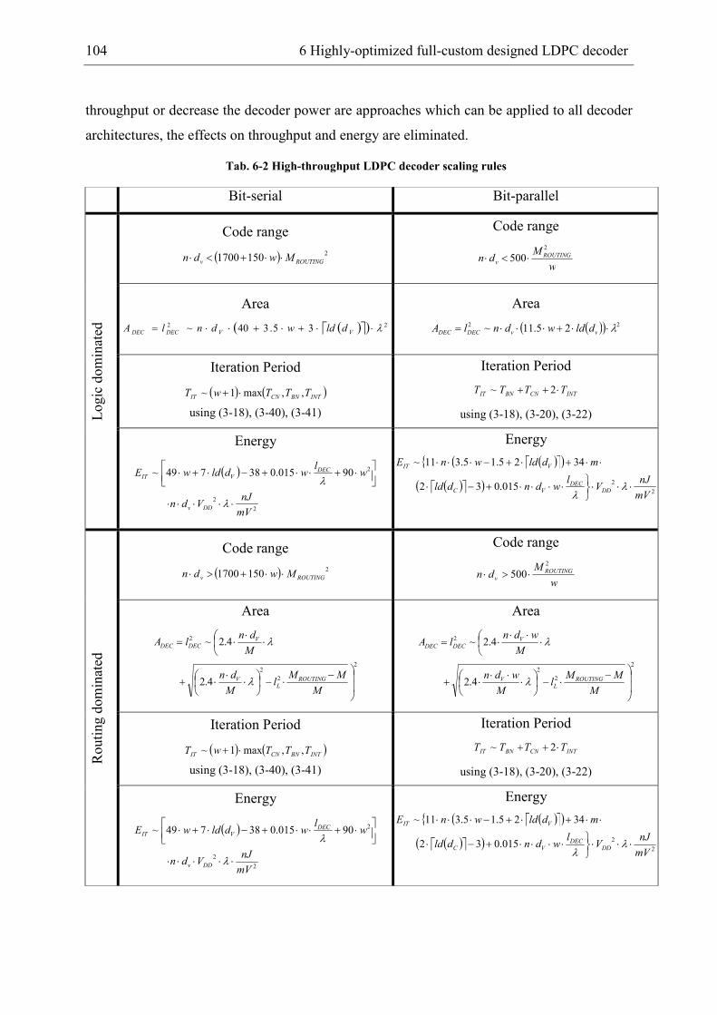
104 6 Highly-optimized full-custom designed LDPC decoder
throughput or decrease the decoder power are approaches which can be applied to all decoder
architectures, the effects on throughput and energy are eliminated.
Tab. 6-2 High-throughput LDPC decoder scaling rules
Bit-serial Bit-parallel
Code range
( ) 21501700 ROUTINGv Mwdn ⋅⋅+<⋅
Code range
w
Mdn ROUTINGv
2
500 ⋅<⋅
Area
( ) ( ) 22 35.340~ λ⋅⋅+⋅+⋅⋅= VVDECDEC dldwdnlA
Area
( )( ) 22 25.11~ λ⋅⋅+⋅⋅⋅= vvDECDEC dldwdnlA
Iteration Period
( ) ( )INTBNCNIT TTTwT ,,max1~ ⋅+
using (3-18), (3-40), (3-41)
Iteration Period
INTCNBNIT TTTT ⋅++ 2~
using (3-18), (3-20), (3-22) Logic dominated
Energy
( )
2
2
290015.038749~
mV
nJVdn
wl
wdldwE
DDv
DECVIT
⋅⋅⋅⋅⋅
⋅+⋅⋅+−⋅+⋅
λ
λ
Energy
( ) ( ){
( ) ( )2
2015.032
3425.15.311~
mV
nJV
lwdndld
mdldwnE
DDDEC
VC
VIT
⋅⋅⋅⋅⋅⋅⋅+−⋅
⋅⋅+⋅+−⋅⋅⋅
λλ
Code range
( ) 21501700 ROUTINGv Mwdn ⋅⋅+>⋅
Code range
w
Mdn ROUTINGv
2
500 ⋅>⋅
Area
2
2
2
2
4.2
4.2~
−⋅−
⋅⋅
⋅+
⋅⋅
⋅=
M
MMl
M
dn
M
dnlA
ROUTINGL
V
VDECDEC
λ
λ
Area
2
2
2
2
4.2
4.2~
−⋅−
⋅
⋅⋅⋅+
⋅
⋅⋅⋅=
M
MMl
M
wdn
M
wdnlA
ROUTINGL
V
VDECDEC
λ
λ
Iteration Period
( ) ( )INTBNCNIT TTTwT ,,max1~ ⋅+
using (3-18), (3-40), (3-41)
Iteration Period
INTCNBNIT TTTT ⋅++ 2~
using (3-18), (3-20), (3-22)
Routing dominated
Energy
( )
2
2
290015.038749~
mV
nJVdn
wl
wdldwE
DDv
DECVIT
⋅⋅⋅⋅⋅
⋅+⋅⋅+−⋅+⋅
λ
λ
Energy
( ) ( ){
( ) ( )2
2015.032
3425.15.311~
mV
nJV
lwdndld
mdldwnE
DDDEC
VC
VIT
⋅⋅⋅⋅⋅⋅⋅+−⋅
⋅⋅+⋅+−⋅⋅⋅
λλ
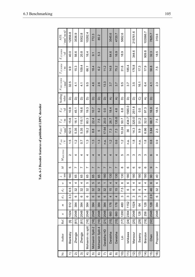
6.3 Benchmarking 105
Tab. 6-3 Decoder features of published LDPC decoder
Nr.
Author
Ref.
nm
dV
dC
wλ
/ nm
MM
ROUTING
VDD
/ V
ADEC
/ mm2
TIT
/ ns
EIT
/ nJ
Scaling
rules
ADEC,NORM
/ mm2
TIT,NORM
/ ns
EIT,NORM
/ nJ
ATE
/ mm2·ns·nJ
1)
Blanksby
[5]
1024
512
3.3
6.5
4160
52
1.5
52.5
15.6
10.8
D)
32.5
9.9
40.0
12856.8
2)
Zhengja
[61]2048
384
632
465
74
1.2
5.35
16.1
45.1
D)
4.1
15.3
56.6
3536.9
3)
Zhengja
[61]2048
384
632
465
74
0.7
5.35
115.1
16.6
D)
4.1
109.4
20.8
9302.8
4)
Mohsenin no split
[16]2048
384
632
565
74
1.3
18.2
80.3
19.3
D)
9.5
66.1
16.4
10282.4
5)
Mohsenin Split-2
[16]2048
384
632
565
74
1.3
8.8
22.4
10.7
D)
4.6
18.4
9.1
772.3
6)
Mohsenin Split-4
[16]2048
384
632
565
74
1.3
57.5
6.2
D)
2.6
6.2
5.3
85.2
7)
Darabiha HD
[21]2048
384
632
1180
74
n.a.
17.64
20.0
0.0
D)
13.3
11.2
8)
Darabiha
[15]
660
176
415
4130
74
1.2
7.3
26.7
18.4
A)
3.7
14.8
64.6
3545.6
9)
Darabiha
[15]
660
176
415
4130
74
0.6
7.3
135.8
4.8
A)
3.7
75.2
16.9
4720.7
10)
Lin
[17]1200
480
37.5
6130
85
1.2
10.24
50.7
6.8
D)
9.5
31.6
18.9
5662.6
11)
Ishikawa
[24]2304
1152
36
6180
63
n.a.
36
434.7
1565.0
D)
3.7
185.4
12)
Mansour
[25]2048
1024
36
4180
63
1.8
14.3
320.0
251.8
D)
3.5
176.8
344.6
215761.6
13)
Swamy
[29]
128
64
36
6180
63
n.a.
9.9
51.2
0.0
C)
16.1
17.3
14)
Brandon
[19]
256
128
34
4180
63
1.8
6.96
32.0
97.3
A)
6.4
17.9
909.8
103566.7
15)
Chen
[32]2048
128
2.9
46
690
96
0.8
3.84
88.7
16.9
D)
4.1
58.8
32.3
7825.7
16)
Proposed
2048
384
632
640
74
0.9
2.3
7.5
18.5
2.3
7.5
18.5
319.6
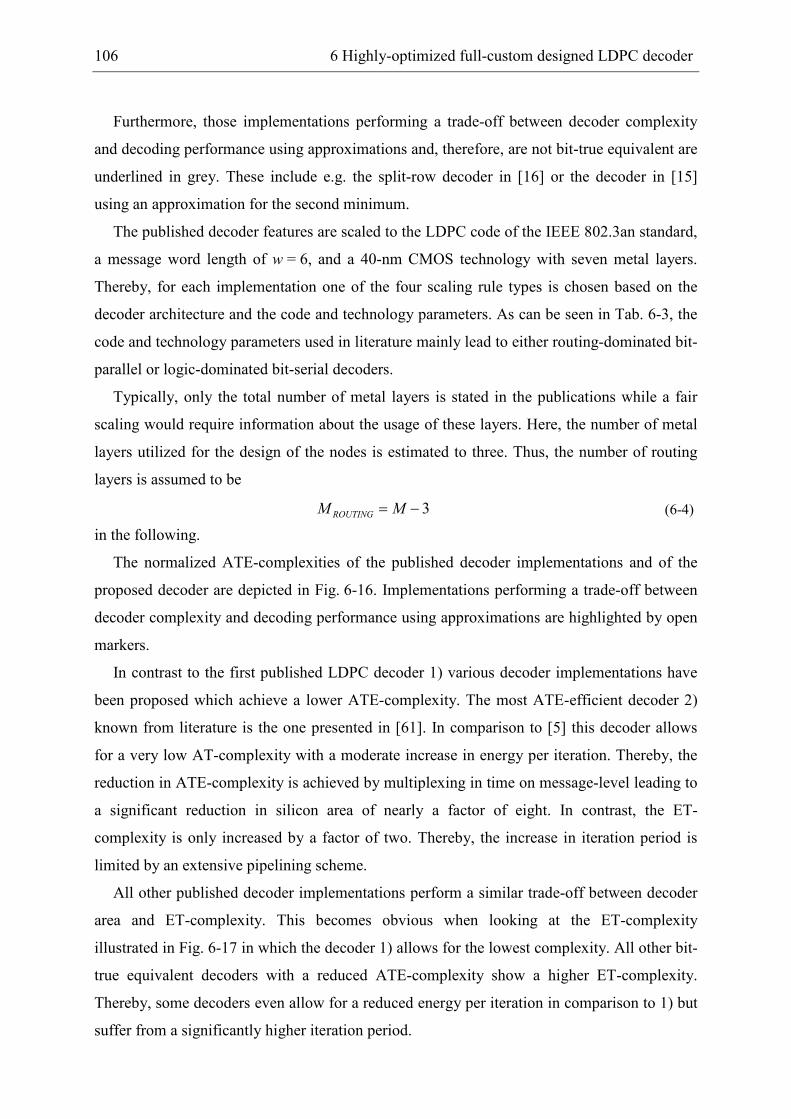
106 6 Highly-optimized full-custom designed LDPC decoder
Furthermore, those implementations performing a trade-off between decoder complexity
and decoding performance using approximations and, therefore, are not bit-true equivalent are
underlined in grey. These include e.g. the split-row decoder in [16] or the decoder in [15]
using an approximation for the second minimum.
The published decoder features are scaled to the LDPC code of the IEEE 802.3an standard,
a message word length of w = 6, and a 40-nm CMOS technology with seven metal layers.
Thereby, for each implementation one of the four scaling rule types is chosen based on the
decoder architecture and the code and technology parameters. As can be seen in Tab. 6-3, the
code and technology parameters used in literature mainly lead to either routing-dominated bit-
parallel or logic-dominated bit-serial decoders.
Typically, only the total number of metal layers is stated in the publications while a fair
scaling would require information about the usage of these layers. Here, the number of metal
layers utilized for the design of the nodes is estimated to three. Thus, the number of routing
layers is assumed to be
3−= MM ROUTING
(6-4)
in the following.
The normalized ATE-complexities of the published decoder implementations and of the
proposed decoder are depicted in Fig. 6-16. Implementations performing a trade-off between
decoder complexity and decoding performance using approximations are highlighted by open
markers.
In contrast to the first published LDPC decoder 1) various decoder implementations have
been proposed which achieve a lower ATE-complexity. The most ATE-efficient decoder 2)
known from literature is the one presented in [61]. In comparison to [5] this decoder allows
for a very low AT-complexity with a moderate increase in energy per iteration. Thereby, the
reduction in ATE-complexity is achieved by multiplexing in time on message-level leading to
a significant reduction in silicon area of nearly a factor of eight. In contrast, the ET-
complexity is only increased by a factor of two. Thereby, the increase in iteration period is
limited by an extensive pipelining scheme.
All other published decoder implementations perform a similar trade-off between decoder
area and ET-complexity. This becomes obvious when looking at the ET-complexity
illustrated in Fig. 6-17 in which the decoder 1) allows for the lowest complexity. All other bit-
true equivalent decoders with a reduced ATE-complexity show a higher ET-complexity.
Thereby, some decoders even allow for a reduced energy per iteration in comparison to 1) but
suffer from a significantly higher iteration period.
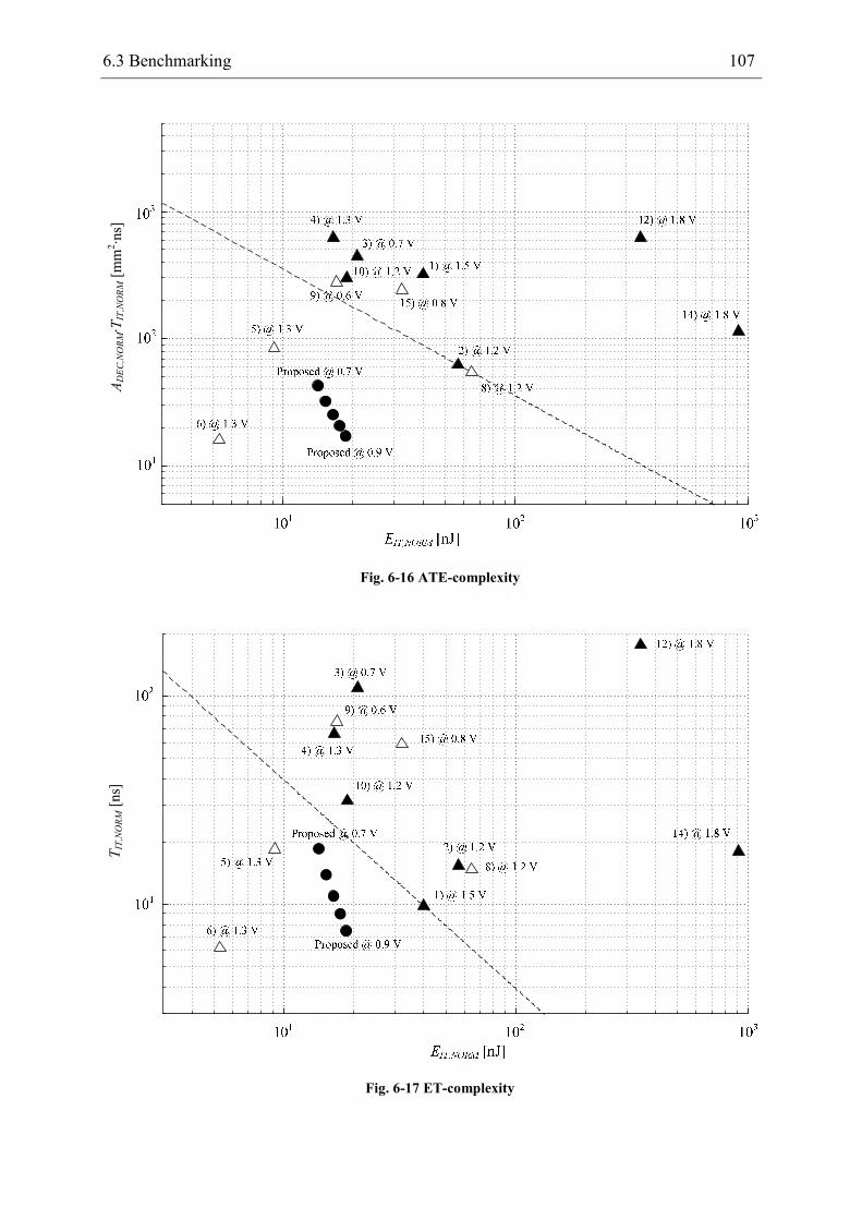
6.3 Benchmarking 107
ADEC,NORM·T
IT,NORM[mm2·ns]
Fig. 6-16 ATE-complexity
TIT,NORM[ns]
Fig. 6-17 ET-complexity
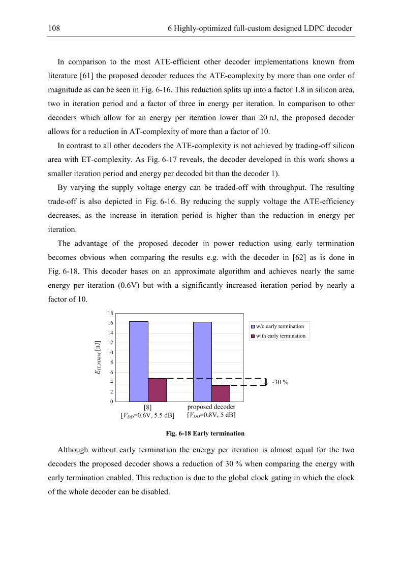
108 6 Highly-optimized full-custom designed LDPC decoder
In comparison to the most ATE-efficient other decoder implementations known from
literature [61] the proposed decoder reduces the ATE-complexity by more than one order of
magnitude as can be seen in Fig. 6-16. This reduction splits up into a factor 1.8 in silicon area,
two in iteration period and a factor of three in energy per iteration. In comparison to other
decoders which allow for an energy per iteration lower than 20 nJ, the proposed decoder
allows for a reduction in AT-complexity of more than a factor of 10.
In contrast to all other decoders the ATE-complexity is not achieved by trading-off silicon
area with ET-complexity. As Fig. 6-17 reveals, the decoder developed in this work shows a
smaller iteration period and energy per decoded bit than the decoder 1).
By varying the supply voltage energy can be traded-off with throughput. The resulting
trade-off is also depicted in Fig. 6-16. By reducing the supply voltage the ATE-efficiency
decreases, as the increase in iteration period is higher than the reduction in energy per
iteration.
The advantage of the proposed decoder in power reduction using early termination
becomes obvious when comparing the results e.g. with the decoder in [62] as is done in
Fig. 6-18. This decoder bases on an approximate algorithm and achieves nearly the same
energy per iteration (0.6V) but with a significantly increased iteration period by nearly a
factor of 10.
0
2
4
6
8
10
12
14
16
18
[8]
[VDD=0.6V, 5.5 dB]
proposed decoder
[VDD=0.8V, 5 dB]
w/o early termination
with early termination
EIT,NORM[nJ]
-30 %
Fig. 6-18 Early termination
Although without early termination the energy per iteration is almost equal for the two
decoders the proposed decoder shows a reduction of 30 % when comparing the energy with
early termination enabled. This reduction is due to the global clock gating in which the clock
of the whole decoder can be disabled.
7 Conclusion
The implementation of highly optimized high-throughput LDPC decoders requires an
optimization of at best all design levels. In this work optimization strategies for various
design levels have been discussed starting on algorithmic level with an analysis of fixed-point
implementations and ending with a full-custom design approach on physical-implementation
level. To allow for a quantitative analysis on the different design levels accurate area, timing,
and energy cost models of high-throughput LDPC decoders have been derived.
On algorithmic level possible fixed-point Sum-Product and Min-Sum decoding algorithms
have been analyzed. Thereby, it has been shown that a linear approximation of the
transcendent Φ function in the Sum-Product algorithm allows for a very attractive decoding
performance. On the other hand for Min-Sum-based decoder implementations it has been
demonstrated that it is possible to choose a post-processing function which simultaneously
allows for an optimal decoding performance and further reduces the decoder complexity.
Subsequently, two new decoder architectures have been introduced. Targeting very high-
throughput applications the new hybrid-cell architecture allows for decoder throughputs close
to the bit-parallel bit- and check-node architecture while reducing the silicon area and energy
per iteration. Additionally, a systematic architectural analysis of bit- and check-node decoders
revealed a new partially bit-serial decoder architecture. This architecture increases the
decoder throughput in comparison to known bit-serial architectures significantly while
maintaining the low area requirements. By adapting the cost models the efficiency of this new
architecture has been shown for almost the complete range of code complexities.
For a further optimization on circuit and physical-implementation level a decoder has been
realized in a 40-nm CMOS technology for an exemplary code. Therefore, the hardware-
efficient post-processing function has been introduced into the partially bit-serial architecture
and the decoder has been designed using a full-custom design approach. The resulting
decoder has been compared to other implementations known from literature in a
benchmarking. As the typically applied scaling rules underestimate the influence of the
interconnect on the decoder throughput and energy per iteration fair scaling rules are derived
based on the accurate area, timing, and energy cost models.
The benchmarking indicates that the performed optimization strategies proposed in the last
seven years at best result in a trade-off between silicon area and ET-complexity. In contrast
the proposed decoder reduces all three decoder metrics. Thereby, the silicon area and the
iteration period is decreased by a factor of about two and the energy per iteration can even be
110 7 Conclusion
reduced by a factor larger than three. In total the proposed decoder allows for an ATE-
complexity which is one order of magnitude smaller than for other high-throughput LDPC
decoder implementations known from literature.
8 Abbreviations
A
Silicon area...................................................... 18
ABCS
Silicon area of a bit compare-and-swap cell.... 24
ABN_P
Silicon area of a bit-parallel bit node .............. 23
ABN_S
Silicon area of bit-serial bit node .................... 37
ABN_S_MOA
Silicon area of multi-operand adder in bit-serial
bit node ....................................................... 36
ABN_S_SAT
Silicon area of saturation unit in bit-serial bit
node ............................................................ 37
AC
Alternating current .......................................... 31
ACN_P
Silicon area of a bit-parallel check node ......... 24
ACN_S
Silicon area of bit-serial check node ............... 35
ACN_S_M_REG
Silicon area of register cells in bit-serial
minimum search ......................................... 34
ACN_S_MIN
Silicon area of minimum search in bit-serial
check node.................................................. 34
ACN_S_SC
Silicon area of minimum-select cells in bit-serial
check node.................................................. 35
ACN_S_STACK
Silicon area of stacks in bit-serial check node. 35
ADEC
Silicon area of decoder macro ......................... 20
ADEC_HC
Silicon area of hybrid-cell decoder.................. 75
ADEC_P
Silicon area of bit-parallel decoder macro....... 45
ADEC_PS
Silicon area of partially bit-serial decoder macro
.................................................................... 89
ADEC_S
Silicon area of bit-serial decoder macro.......... 45
AFA
Silicon area of a full adder .............................. 23
AHA
Silicon area of a half adder........................ 22, 23
AL_P
Silicon area of bit-parallel decoder logic ........ 24
AL_PS
Silicon area of new partially bit-serial decoder
logic............................................................ 89
AL_S
Silicon area of bit-serial LDPC decoder logic. 37
AMUX
Silicon area of a multiplexer ........................... 34
AR_P
Routing area of a bit-parallel LDPC decoder .. 30
AR_S
Routing area of a bit-serial LDPC decoder ..... 37
AREG
Silicon area of a register.................................. 34
ATE-complexity
Area-timing-energy product ............................ 20
ATEP
Area-timing-energy product of bit-parallel
decoder ....................................................... 45
ATEPS
Area-timing-energy product of partially bit-
serial decoder.............................................. 89
ATES
Area-timing-energy product of bit-serial decoder
.................................................................... 45
AXOR
Silicon area of a xor gate................................. 23
B
Number of interleaved blocks in an LDPC
decoder ....................................................... 19
112 8 Abbreviations
BCS-cell
Bit compare-and-swap cell .............................. 24
BER
Bit-error rate.................................................... 19
BPSK
Binary phase shift keying ................................ 11
c
Costs of a specific placement during the
simulated annealing algorithm.................... 26
C’
Interconnect capacitance per unit length ......... 31
CREG_IN
Capacitance at clock input of register ............. 38
dB
Decibel ............................................................ 31
dC
Check-node degree.......................................... 11
DC
Direct current ................................................ 101
dV
Bit node degree ............................................... 11
E
Energy per operation ....................................... 18
EBCS
Average energy of a bit compare-and-swap
operation..................................................... 33
ECLK_CYC_S
Energy per clock cycle of bit-serial LDPC
decoder: clock fraction ............................... 38
ECLK_PS
Energy per iteration of new partially bit-serial
decoder: clock fraction ............................... 89
ECLK_S
Energy per iteration of bit-serial LDPC decoder:
clock fraction .............................................. 38
EDEC_PS
Energy per iteration of new partially bit-serial
decoder ....................................................... 89
EFA
Average energy of a full-adder operation........ 33
EINT_P
Energy per iteration of bit-parallel LDPC
decoder: interconnect fraction .................... 32
EINT_PS
Energy per iteration of new partially bit-serial
decoder: interconnect fraction .................... 89
EINT_S
Energy per iteration of bit-serial LDPC decoder:
interconnect fraction................................... 39
EIT
Energy per decoding iteration ......................... 20
EIT_P
Energy per iteration of bit-parallel LDPC
decoder ....................................................... 33
EIT_S
Energy per iteration of bit-serial LDPC decoder
.................................................................... 39
EL_P
Energy per iteration of bit-parallel LDPC
decoder: logic fraction................................ 33
EL_PS
Energy per iteration of new partially bit-serial
decoder: logic fractio.................................. 89
EL_S
Energy per iteration of bit-serial LDPC decoder:
logic fraction .............................................. 39
FA
Full adder ........................................................ 22
fBLOCK
Decoder block throughput ............................... 19
FER
Frame-error rate .............................................. 19
G
LDPC generator matrix ..................................... 9
H
LDPC parity-check matrix .............................. 10
HA
Half adder........................................................ 22
HC
Hybrid cell....................................................... 69
8 Abbreviations 113
HDL
Hardware description language ....................... 49
IMAX
Maximum number of decoding iterations ....... 19
L(ci)
Received log-likelihood information of symbol i
.................................................................... 10
L(Qi)
Updated log-likelihood information of symbol i
.................................................................... 10
L(qij)
Extrinsic log-likelihood information of symbol i
for parity check j......................................... 12
L(ri)
A-posteriori information for symbol i ............. 10
L(rij)
A-posteriori information of symbol i from SISO
decoder j, for LDPC decoder j indicates the
parity check ................................................ 10
lAVAIL
Available Manhattan length in CMOS metal
stack............................................................ 29
lAVG
Average Manhattan length of one interconnect
line between one bit and one check node ... 25
lCNA
Silicon area of check-node array logic ............ 28
lDEC
Macro side length of LDPC decoder ............... 25
lDEC_P
Macro side length of bit-parallel LDPC decoder
.................................................................... 28
lDEC_S
Macro side length of bit-serial LDPC decoder 37
lL_P
Macro side length of bit-parallel LDPC decoder
logic ............................................................ 30
lL_S
Macro side length of bit-serial LDPC decoder
logic ............................................................ 37
lMAX
Maximum Manhattan length of one interconnect
line between one bit and one check node ... 27
lREQ
Required Manhattan length of all bit- and check-
node connections in a bit-parallel LDPC
decoder ....................................................... 25
LSB
Least-significant bit......................................... 23
LTEMP_i-1(Rj)
Intermediate result of L(Rj) considering all
symbols i’<i................................................ 70
LTEMP_j-1(Qi)
Intermediate result of L(Qi) considering all
parity checks j’<j ........................................ 70
m
Blocklength of information vector x ................. 9
M
Number of metal layers in CMOS metal stack 30
MROUTING
Number of metal layers in CMOS metal stack
used for routing .......................................... 29
MSB
Most-significant bit ......................................... 16
n
Blocklength of code vector y............................. 9
n1, n2
Normally distributed random variables ........... 50
NBN_P_FA
Number of full adders in bit-parallel bit node . 22
NCC_AVG
Average number of active clock cycles in an
LDPC decoder .......................................... 104
NCN_P_CS
Number of compare and swap elements in a bit-
parallel check node..................................... 23
NDEC_PS_REG
Number of registers in new partially bit-serial
LDPC decoder ............................................ 89
NDEC_S_REG
114 8 Abbreviations
Number of registers in bit-serial LDPC decoder
.................................................................... 38
p
Routing pitch................................................... 29
PCLK
Power dissipation of an LDPC decoder
clock fraction ............................................ 103
PDEC
Dynamic power dissipation of an LDPC decoder
.................................................................. 103
PDEC_PS
Power consumption of partially bit-serial
decoder ..................................................... 101
P'DYN
Dynamic power dissipation of an LDPC decoder
with early termination............................... 103
P''DYN
Dynamic power dissipation of an LDPC decoder
with clock gating ...................................... 104
Pi(z)
Polynomials used in Tausworthe generator..... 51
Qi
Quantization domain in LDPC decoder loop .. 53
r
Radius in two-dimensional normal distribution
.................................................................... 50
R
Code rate ........................................................... 9
R’
Interconnect resistance per unit length ............ 31
SISO decoder
Soft-input soft-output decoder......................... 10
SNR
Signal-to-noise ratio ........................................ 31
T
Timing metric.................................................. 18
TBCS
Propagation delay of a bit compare-and-swap
cell .............................................................. 31
TBLOCK
Inverse of decoder block throughput............... 19
TBN_P
Propagation delay of bit-parallel bit node ....... 31
TBN_S
Propagation delay of bit-serial bit node .......... 38
TCN_P
Propagation delay of a bit-parallel check node 31
TCN_PS
Propagation delay of check node in new partially
bit-serial decoder architecture .................... 89
TCN_S
Propagation delay of bit-serial check node ..... 38
Temp
Temperature in simulated annealing algorithm26
TFA
Propagation delay of a full adder .................... 31
TINT_P
Propagation delay of longest interconnect line in
bit-parallel LDPC decoder.......................... 30
TINT_S
Propagation delay of longest interconnect line in
bit-serial LDPC decoder ............................. 38
TIT
Iteration period................................................ 19
TIT_HC
Iteration period of hybrid-cell decoder............ 75
TIT_P
Iteration period of a bit-parallel LDPC decoder
.................................................................... 31
TIT_PS
Iteration period of new partially bit-serial
decoder ....................................................... 89
TIT_S
Iteration period of a bit-serial LDPC decoder . 38
TL
Block latency................................................... 19
TLOAD
Time to load information of received block into
LDPC decoder ............................................ 19
TPMP
8 Abbreviations 115
Two-phase message passing............................ 13
tsC
Tree stages in hybrid-cell’s check-node
calculation .................................................. 71
tsV
Tree stages in hybrid-cell’s bit-node calculation
.................................................................... 71
u
Utilization of metal layers ............................... 29
u1, u2
Uniformly distributed random variables ......... 50
w
Word length of communicated messages
between bit and check nodes ...................... 21
wA-PRIORI
Word length of A-priori information L(ci) ...... 20
wC1........................................................................ 53
Word length in quantization domain Qi........... 53
wDIGIT
Number of parallel communicated bits in a digit-
serial decoder.............................................. 90
wEXT_BN
Extended word length in bit node.................... 22
wEXT_CN
Extended word length in check node............... 53
wIN
Word length of decoder input stream .............. 19
x
Information vector............................................. 9
y
Code vector ....................................................... 9
y'
Received noisy code vector ............................. 10
β
Offset value for offset post-processing functions
.................................................................... 62
γ
Power consumption overhead of early
termination control logic .......................... 104
∆cNORM
Normalized cost difference in annealing
algorithm .................................................... 26
ε
Output threshold for offset post-processing
functions ..................................................... 62
η
Input threshold for offset post-processing
functions ..................................................... 62
λ
Technology feature size .................................. 39
µ
Mean value of normally distributed variable... 50
ν
Ratio between average and maximum number of
active clock cycles in an LDPC decoder .. 104
ξ
Correction factor for interconnect capacitance
calculation .................................................. 32
ρAVG
Average interconnect density .......................... 30
ρMAX
Maximum interconnect density ....................... 30
σ2
Standard deviation of normally distributed
variable ....................................................... 12
φ
Angle in two-dimensional normal distribution 50
ωi
Weights for weighted cost calculation in
simulated annealing algorithm ................... 73
Ф’
Linear approximation of Ф-function ............... 60
Ф-function
( )
=Φ2
xx tanhlog ................................ 13

9 Bibliography
[1] R. Gallager: "Low-density parity-check codes," Information Theory, IRE Transactions on,
vol. 8, pp. 21-28, 1962.
[2] C. Sae-Young, G. D. Forney, Jr., et al.: "On the design of low-density parity-check codes
within 0.0045 dB of the Shannon limit," Communications Letters, IEEE, vol. 5, pp.
58-60, 2001.
[3] A. Viterbi: "Error bounds for convolutional codes and an asymptotically optimum
decoding algorithm," Information Theory, IEEE Transactions on, vol. 13, pp. 260-
269, 1967.
[4] C. Berrou, A. Glavieux, et al.: "Near Shannon limit error-correcting coding and decoding:
Turbo-codes. 1," in Communications, 1993. ICC 93. Geneva. Technical Program,
Conference Record, IEEE International Conference on, 1993, pp. 1064-1070 vol.2.
[5] A. J. Blanksby, C. J. Howland: "A 690-mW 1-Gb/s 1024-b, Rate-1/2 Low-Density Parity-
Check Code Decoder," Solid-State Circuits, IEEE Journal of, vol. 37, pp. 404-412,
2002.
[6] IEEE: "IEEE Standard for Information Technology-Telecommunications and Information
Exchange Between Systems-Local and Metropolitan Area Networks-Specific
Requirements Part 3: Carrier Sense Multiple Access With Collision Detection
(CSMA/CD) Access Method and Physical Layer Specifications," IEEE Std 802.3an-
2006 (Amendment to IEEE Std 802.3-2005), pp. 0_1-167, 2006.
[7] V. Oksman, S. Galli: "G.hn: The new ITU-T home networking standard,"
Communications Magazine, IEEE, vol. 47, pp. 138-145, 2009.
[8] IEEE: "802.11n. Wireless LAN Medium Access Control and Physical Layer
specifications: Enhancements for Higher Throughput. IEEE P802.16n/D1.0, Mar
2006," 2006.
[9] IEEE: "802.16e. Air Interface for Fixed and Mobile Broadband Wireless Access Systems.
IEEE P802.16e/D12 Draft, oct 2005," 2005.
[10] "European Telecommunications Standards Institude (ETSI). Digital Video Broadcasting
(DVB) Second generation framing structure for broadband satellite applications; EN
302 307 V1.1.1 www.dvb.org."
[11] W. Zhang, Y. Guan, et al.: "An Introduction of the Chinese DTTB Standard and Analysis
of the PN595 Working Modes," Broadcasting, IEEE Transactions on, vol. 53, pp. 8-
13, 2007.
[12] R. L. Galbraith, T. Oenning, et al.: "Architecture and Implementation of a First-
Generation Iterative Detection Read Channel," Magnetics, IEEE Transactions on, vol.
46, pp. 837-843.
[13] M. P. C. Fossorier, M. Mihaljevic, et al.: "Reduced complexity iterative decoding of low-
density parity check codes based on belief propagation," Communications, IEEE
Transactions on, vol. 47, pp. 673-680, 1999.
[14] C. Jinghu, M. P. C. Fossorier: "Near optimum universal belief propagation based
decoding of low-density parity check codes," Communications, IEEE Transactions on,
vol. 50, pp. 406-414, 2002.
[15] A. Darabiha, A. C. Carusone, et al.: "A 3.3-Gbps Bit-Serial Block-Interlaced Min-Sum
LDPC Decoder in 0.13-µm CMOS," in Custom Integrated Circuits Conference, 2007.
CICC '07. IEEE, 2007, pp. 459-462.
[16] T. Mohsenin, D. Truong, et al.: "Multi-Split-Row Threshold decoding implementations
for LDPC codes," in Circuits and Systems, 2009. ISCAS 2009. IEEE International
Symposium on, 2009, pp. 2449-2452.
118 9 Bibliography
[17] C.-C. Lin, K.-L. Lin, et al.: "A 3.33Gb/s (1200,720) low-density parity check code
decoder," in Solid-State Circuits Conference, 2005. ESSCIRC 2005. Proceedings of
the 31st European, 2005, pp. 211-214.
[18] M. Karkooti, P. Radosavljevic, et al.: "Configurable, High Throughput, Irregular LDPC
Decoder Architecture: Tradeoff Analysis and Implementation," in Application-specific
Systems, Architectures and Processors, 2006. ASAP '06. International Conference on,
2006, pp. 360-367.
[19] T. Brandon, R. Hang, et al.: "A scalable LDPC decoder ASIC architecture with bit-serial
message exchange," Integr. VLSI J., vol. 41, pp. 385-398, 2008.
[20] M. Cocco, J. Dielissen, et al.: "A scalable architecture for LDPC decoding," in Design,
Automation and Test in Europe Conference and Exhibition, 2004. Proceedings, 2004,
pp. 88-93 Vol.3.
[21] A. Darabiha, A. C. Carusone, et al.: "Multi-Gbit/sec low density parity check decoders
with reduced interconnect complexity," in Circuits and Systems, 2005. ISCAS 2005.
IEEE International Symposium on, 2005, pp. 5194-5197 Vol. 5.
[22] Y. Engling, N. Borivoje: "A 1.1-Gb/s 4092-bit Low-Density Parity-Check Decoder," in
Asian Solid-State Circuits Conference, 2005, 2005, pp. 237-240.
[23] P. Urard, E. Yeo, et al.: "A 135Mb/s DVB-S2 compliant codec based on 64800b LDPC
and BCH codes," in Solid-State Circuits Conference, 2005. Digest of Technical
Papers. ISSCC. 2005 IEEE International, 2005, pp. 446-609 Vol. 1.
[24] T. Ishikawa, K. Shimizu, et al.: "High-throughput decoder for low-density parity-check
code," in Design Automation, 2006. Asia and South Pacific Conference on, 2006, p. 2
pp.
[25] M. M. Mansour, N. R. Shanbhag: "A 640-Mb/s 2048-bit programmable LDPC decoder
chip," Solid-State Circuits, IEEE Journal of, vol. 41, pp. 684-698, 2006.
[26] T. Brack, M. Alles, et al.: "Low Complexity LDPC Code Decoders for Next Generation
Standards," in Design, Automation & Test in Europe Conference & Exhibition, 2007.
DATE '07, 2007, pp. 1-6.
[27] K. Se-Hyeon, P. In-Cheol: "Loosely coupled memory-based decoding architecture for
low density parity check codes," Circuits and Systems I: Regular Papers, IEEE
Transactions on, vol. 53, pp. 1045-1056, 2006.
[28] K. K. Gunnam, G. S. Choi, et al.: "VLSI Architectures for Layered Decoding for
Irregular LDPC Codes of WiMax," in Communications, 2007. ICC '07. IEEE
International Conference on, 2007, pp. 4542-4547.
[29] R. Swamy, S. Bates, et al.: "Design and Test of a 175-Mb/s, Rate-1/2 (128,3,6) Low-
Density Parity-Check Convolutional Code Encoder and Decoder," Solid-State
Circuits, IEEE Journal of, vol. 42, pp. 2245-2256, 2007.
[30] S. Yang, M. Karkooti, et al.: "VLSI Decoder Architecture for High Throughput, Variable
Block-size and Multi-rate LDPC Codes," in Circuits and Systems, 2007. ISCAS 2007.
IEEE International Symposium on, 2007, pp. 2104-2107.
[31] M. Bimberg, M. B. S. Tavares, et al.: "A High-Throughput Programmable Decoder for
LDPC Convolutional Codes," in Application -specific Systems, Architectures and
Processors, 2007. ASAP. IEEE International Conf. on, 2007, pp. 239-246.
[32] C. Chih-Lung, L. Kao-Shou, et al.: "A 11.5-Gbps LDPC decoder based on CP-PEG code
construction," in ESSCIRC, 2009. ESSCIRC '09. Proceedings of, 2009, pp. 412-415.
[33] S. Jin, W. Zhongfeng, et al.: "Multi-Gb/s LDPC Code Design and Implementation," Very
Large Scale Integration (VLSI) Systems, IEEE Transactions on, vol. 17, pp. 262-268,
2009.
9 Bibliography 119
[34] Z. Zhang, L. Dolecek, et al.: "Low error rate LDPC decoders," in Signals, Systems and
Computers, 2009 Conference Record of the Forty-Third Asilomar Conference on,
2009, pp. 1278-1282.
[35] B. Xiang, R. Shen, et al.: "An Area-Efficient and Low-Power Multirate Decoder for
Quasi-Cyclic Low-Density Parity-Check Codes," Very Large Scale Integration (VLSI)
Systems, IEEE Transactions on, vol. PP, pp. 1-1, 2009.
[36] H. Shuangqu, X. Bo, et al.: "A flexible architecture for multi-standard LDPC decoders,"
in ASIC, 2009. ASICON '09. IEEE 8th International Conference on, 2009, pp. 493-
496.
[37] J. Nan, P. Kewu, et al.: "High-Throughput QC-LDPC Decoders," Broadcasting, IEEE
Transactions on, vol. 55, pp. 251-259, 2009.
[38] X.-Y. Shih, C.-Z. Zhan, et al.: "A 52-mW 8.29mm2 19-mode LDPC decoder chip for
Mobile WiMAX applications," in Design Automation Conference, 2009. ASP-DAC
2009. Asia and South Pacific, 2009, pp. 121-122.
[39] Z. Zhengya, V. Anantharam, et al.: "An Efficient 10GBASE-T Ethernet LDPC Decoder
Design With Low Error Floors," Solid-State Circuits, IEEE Journal of, vol. 45, pp.
843-855.
[40] M. Korb, T. G. Noll: "Towards a Scaling Model for Fair Benchmarking of LDPC
Decoder Architectures," www.eecs.rwth-aachen.de.
[41] M. Korb, T. G. Noll: "Area and Latency Optimized High-Throughput Min-Sum Based
LDPC Decoder Architectures," in ESSCIRC, 2009, pp. 408-411.
[42] D. E. Knuth: The Art of Computer Programming Volume 3 Sorting and Searching:
Addison-Wesley, 1973.
[43] C. Henning, T. G. Noll: "Architecture and implementation of a bitserial sorter for
weighted median filtering," in Custom Integrated Circuits Conference, 1998.
Proceedings of the IEEE 1998, 1998, pp. 189-192.
[44] D. MacKay: "http://www.inference.phy.cam.ac.uk/mackay/codes/data.html." vol. 2009.
[45] M. Korb, T. G. Noll: "LDPC decoder area, timing, and energy models for early
quantitative hardware cost estimates," in System on Chip (SoC), 2010 International
Symposium on, 2010, pp. 169-172.
[46] R. Ho, K. W. Mai, et al.: "The future of wires," Proceedings of the IEEE, vol. 89, pp.
490-504, 2001.
[47] "http://embedded.eecs.berkeley.edu/pubs/downloads/espresso/." vol. 2008.
[48] Z. Zhengya, L. Dolecek, et al.: "Investigation of Error Floors of Structured Low-Density
Parity-Check Codes by Hardware Emulation," in Global Telecommunications
Conference, 2006, IEEE, 2006, pp. 1-6.
[49] T. Richardson: "Error floors of LDPC codes," in Allerton Conference on
Communications, Control, and Computing, 2003.
[50] D. U. Lee, J. D. Villasenor, et al.: "A hardware Gaussian noise generator using the Box-
Muller method and its error analysis," Computers, IEEE Transactions on, vol. 55, pp.
659-671, 2006.
[51] G. Box, M. Muller: "A Note on the Generation of Random Normal Deviates," Annals
Math. Statistics, vol. 29, pp. 610-611 1958
[52] P. L'Ecuyer: "Maximally Equidistributed Combined Tausworthe Generators," Math.
Computation, vol. 65, pp. 203-213, 1996
[53] B. Sklar: Digital Communication, Fundamentals and Applications, 2 ed.: Prentice Hall,
2002.
[54] "www.eve-team.com/products/datasheets/ax.php," in White Paper ZeBU-AX. vol. 2009.
120 9 Bibliography
[55] S. L. Howard, C. Schlegel, et al.: "A degree-matched check node approximation for
LDPC decoding," in Information Theory, 2005. ISIT 2005. Proceedings. International
Symposium on, 2005, pp. 1131-1135.
[56] G. Lechner, T. Pedersen, et al.: "EXIT Chart Analysis of Binary Message-Passing
Decoders," in Information Theory, 2007. ISIT 2007. IEEE International Symposium
on, 2007, pp. 871-875.
[57] M. Korb, T. G. Noll: "Area- and energy-efficient high-throughput LDPC decoders with
low block latency," in ESSCIRC (ESSCIRC), 2011 Proceedings of the, 2011, pp. 75-
78.
[58] Cadence: "ICCraftsman," 11.2.41 ed.
[59] T. Mohsenin, B. M. Baas: "High-Throughput LDPC Decoders Using A Multiple Split-
Row Method," in Acoustics, Speech and Signal Processing, 2007. ICASSP 2007. IEEE
International Conference on, 2007, pp. II-13-16.
[60] O. Weiss, M. Gansen, et al.: "A flexible datapath generator for physical oriented design,"
in ESSCIRC, 2001, pp. 393-396.
[61] Z. Zhang, V. Anantharam, et al.: "A 47 Gb/s LDPC Decoder With Improved Low Error
Rate Performance," in VLSI Circuits, 2009 Symposium on, 2009, pp. 286-287.
[62] A. Darabiha, A. Chan Carusone, et al.: "Power Reduction Techniques for LDPC
Decoders," Solid-State Circuits, IEEE Journal of, vol. 43, pp. 1835-1845, 2008.
[63] T. Mohsenin, B. Baas: "A Split-Decoding Message Passing Algorithm for Low Density
Parity Check Decoders," Journal of Signal Processing Systems, pp. 1-17, 2010.
Curriculum vitae
Name Matthias Korb
Date of birth 12th of November 1979
City of birth Arnsberg, Germany
Education
1986 – 1990 Heinrich-Knoche-Grundschule, Arnsberg, Germany
1990 – 1999 Graf-Gottfried-Gymnasium, Arnsberg, Germany
05/1999 General Qualification for University Entrance
2000 - 2006 RWTH Aachen University, Germany
Electrical Engineering and Information Technology
Specialization: Information and Communication Engineering
04/2006 Diploma Electrical Engineering and Information Technology
since 2003 Fern Universitaet Hagen, Germany (Open University)
Business Administration and Economics
09/2006 Prediploma Business Administration and Economics
Professional Experience
1999 – 2000 Community Service
Environmental Office Arnsberg, Germany
since 2006 Research and Teaching Assistant
Institute for Electrical Engineering and Computer Systems (EECS),
RWTH Aachen University, Germany