Embed Size (px)
Citation preview
Deep level transient spectroscopy of vertically stacked
InAs/Al0.5Ga0.5As self-assembled quantum dots
Shuwei Lia,*, Kazuto Koikeb, Shigehiko Sasab, Masataka Inoueb,Mitsuaki Yanob, Yixin Jinc
aDepartment of Physics, The State Key Laboratory of Optoelectronic Materials and Technologies, Zhongshan (Sun Yat-sen) University,
No. 135, XinGangXi Road, Guangzhou 510275, People’s Republic of ChinabNew Materials Research Center, Osaka Institute of Technology, Asahi-ku Ohmiya, Osaka 535-8585, Japan
cChangchun Institute of Optics, Fine Mechanics and Physics, Chinese Academy of Sciences, No. 1 Yan-an Road,
130021 Changchun, People’s Republic of China
Received 5 March 2002; received in revised form 14 March 2003; accepted 4 April 2003 by H. Akai
Abstract
Quantum dots (QDs), which capture and emit carriers like a giant trap, are studied using deep level transient spectroscopy
(DLTS). The electrons and holes in the QDs are emitted from the relevant energy levels to the conduction and valence bands,
respectively, of the barrier layers with increasing temperature. The thermal emission energies from the QDs are related to their
initial energy levels. In this paper, five-period vertically stacked InAs QDs in the barrier layers of a field-effect type structure are
measured. The results agree well with capacitance–voltage and photoluminescence measurements. In addition, the dependence
of DLTS signal on the pulse voltage and light illumination is presented. The results prove that DLTS is a powerful tool for the
study of the electronic structure of QDs.
q 2003 Elsevier Science Ltd. All rights reserved.
PACS: 73.20.Dx; 68.65. þ g; 71.55.Eg; 61.82.Fk
Keywords: A. Semiconductors; B. Epitaxy; D. Recombination and trapping
Deep levels often behave as carrier traps or as generation
and recombination centers. For this reason, the deep level
transient spectroscopy (DLTS) established by Lang has been
widely used to investigate the properties of deep levels [1,2].
Quantum dots (QDs) acting as giant traps can capture and
emit carriers from the barrier regions in the same way as
deep levels. In this paper, the self-assembled QDs with large
confinement potentials, which are used to store charges as
memory devices [3], are studied by DLTS. Capacitance–
voltage (C–V) measurement for QSs is also performed to
clarify the electronic structure [4,5]. The thermal emission
from the QDs with large confinement potentials might be
able to mask the emission from the deep levels in the DLTS
data since the latter has exponential dependence on the
binding energy with increasing temperature [6]. To know
the position of the QD energy levels, particularly of the
ground state, is of primary importance. These discrete
energy levels are described by use of the DLTS data and are
compared with the C–V and photoluminescence (PL)
results.
The sample is first cooled down below 90 K using liquid
nitrogen and then heated until 400 K. In the PL measure-
ment the sample is in a closed-cycle He cryostat (20–300 K)
and excited by a 514.5 nm line of Arþ ion laser as an
excitation source. The sample in this study is 5-period
vertically stacked InAs QDs in an Al0.5Ga0.5As barrier layer
grown by molecular beam epitaxy using solid sources of Al,
Ga, In, and As in non-cracking K-cells [6,7]. The structure
of the QD sample consists of a 500 nm Si-doped GaAs
buffer layer on Si-doped GaAs substrate, a 500 nm GaAs
0038-1098/03/$ - see front matter q 2003 Elsevier Science Ltd. All rights reserved.
doi:10.1016/S0038-1098(03)00299-0
Solid State Communications 126 (2003) 563–566
www.elsevier.com/locate/ssc
* Corresponding author. Tel.: þ86-208-411-4899; fax: þ86-208-
411-3575.
E-mail address: [email protected] (S. Li).
layer, a 15 nm Al0.5Ga0.5As barrier layer, 5-periods of
vertically stacked InAs QDs after depositing 2 monolayers
of GaAs smoothing layer, a 50 nm Al0.5Ga0.5As barrier
layer, and a 15 nm GaAs cap layer. The QDs at respective
period are about 3 nm high and about 30 nm wide in size,
and about 1 £ 1010 cm22 in density, which are vertically
separated by 5 nm thick spacer layers each other.
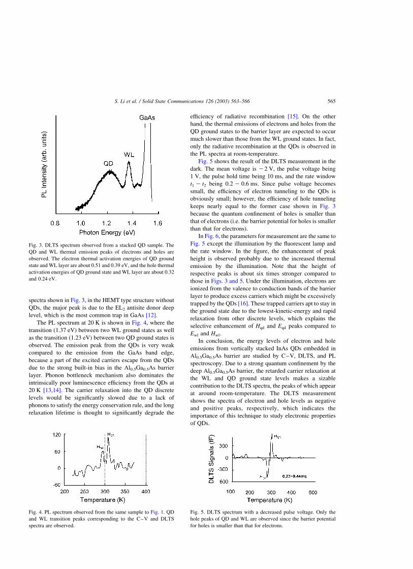
In Fig. 1, the surface morphology of the first and fifth
sheets are shown together with the histograms of width and
height of the dots. The atomic force microscopy data show
no big difference between the first and fifth QD layer as is
seen in the histograms. This indicates that the vertically
stacked QDs are homogeneously distributed, which enables
the strong confinement in the vertical stacking of InAs QDs.
The DLTS and C–V measurements were carried out
using standard technique in New Materials Research Center,
Osaka Institute of Technology and performed using a HP
4280A 1 MHz capacitance meter, a pulse generator, and a
temperature controller. The measurement process is con-
trolled by a computer: the different rate window signals of
the capacitance meter, which are regulated by the computer
controlled generator, are applied to Au metal electrode
(about 1 mm2) of the sample surface and In metal electrode
on the sample rear, the sample temperature is varied within
90–400 K range.
C–V measurement is known to be a very powerful
technique to obtain the concentration and distribution of
carriers, band offsets, density of states and other parameters
of the semiconductors [8]. The signals related to wetting
layer (WL) and QDs might be obtained by the C–V
measurement at 77 K using a back contact geometry [9,10].
The capacitance spectrum in Fig. 2 is obtained under the
illumination by a fluorescent lamp and dc bias which is used
to move the Fermi level in the Al0.5Ga0.5As band gap. At
U , 21:3 V; both the ground states of QDs and WL are
above the Fermi level. At U , 21:2 V; the ground state of
QDs is shifted below the Fermi level, and electrons become
to tunnel from the back contact into each QD. With
increasing the bias voltage, the QD ground state continues to
be charged, and the tunneling into the QDs is shown by the
broad shoulder between 21:2 V , U , 20:4 V: At U
about 20.2 V, the ground state of WL is shifted below
the Fermi level. Therefore, more electrons start to tunnel
from the back contact into the two-dimensional (2D) WL,
and then a plateau is observed in the C–V curve due to the
successive electron tunneling through the high potential
barrier of Al0.5Ga0.5As, which is one of characteristics of the
QD structure under the illumination.
QDs may be characterized by three parameters: an
activation energy which is the position of the energy level in
the band gap, the concentration, and the capture cross
section which provides a measure of the ability of QDs to
trap carriers. The signal of DLTS is the difference between
capacitances measured at times t1 2 t2; namely Cðt1Þ2
Cðt2Þ; and the overall signal amplitude from the QD samples
over the entire range of scanned temperature is found to be
higher than that without QDs. The sign of the peaks
indicates the type of trapped carriers (i.e. the positive signal
corresponds to a hole energy level, and the negative one to
an electron trapping energy level), the height of the peaks is
proportional to the concentration, and the position, in the
scanned temperature, of the peaks is uniquely determined by
the degree of carrier confinement [11]. Some papers have
reported that DLTS peaks of InAs/GaAs self-assembled
QDs locate at low temperature regions (typically below
100 K) due to the small activation energy [4,11]. In the case
of InAs/Al0.5Ga0.5As QDs with high potential barrier,
however, it is reasonable to expect the QD DLTS signals
to appear at around room-temperature.
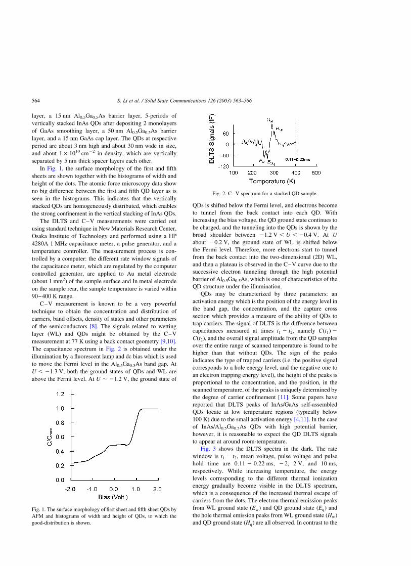
Fig. 3 shows the DLTS spectra in the dark. The rate
window is t1 2 t2; mean voltage, pulse voltage and pulse
hold time are 0.11 2 0.22 ms, 22, 2 V, and 10 ms,
respectively. While increasing temperature, the energy
levels corresponding to the different thermal ionization
energy gradually become visible in the DLTS spectrum,
which is a consequence of the increased thermal escape of
carriers from the dots. The electron thermal emission peaks
from WL ground state ðEwÞ and QD ground state ðEqÞ and
the hole thermal emission peaks from WL ground state ðHwÞ
and QD ground state ðHqÞ are all observed. In contrast to the
Fig. 1. The surface morphology of first sheet and fifth sheet QDs by
AFM and histograms of width and height of QDs, to which the
good-distribution is shown.
Fig. 2. C–V spectrum for a stacked QD sample.
S. Li et al. / Solid State Communications 126 (2003) 563–566564
spectra shown in Fig. 3, in the HEMT type structure without
QDs, the major peak is due to the EL2 antisite donor deep
level, which is the most common trap in GaAs [12].
The PL spectrum at 20 K is shown in Fig. 4, where the
transition (1.37 eV) between two WL ground states as well
as the transition (1.23 eV) between two QD ground states is
observed. The emission peak from the QDs is very weak
compared to the emission from the GaAs band edge,
because a part of the excited carriers escape from the QDs
due to the strong built-in bias in the Al0.5Ga0.5As barrier
layer. Phonon bottleneck mechanism also dominates the
intrinsically poor luminescence efficiency from the QDs at
20 K [13,14]. The carrier relaxation into the QD discrete
levels would be significantly slowed due to a lack of
phonons to satisfy the energy conservation rule, and the long
relaxation lifetime is thought to significantly degrade the
efficiency of radiative recombination [15]. On the other
hand, the thermal emissions of electrons and holes from the
QD ground states to the barrier layer are expected to occur
much slower than those from the WL ground states. In fact,
only the radiative recombination at the QDs is observed in
the PL spectra at room-temperature.
Fig. 5 shows the result of the DLTS measurement in the
dark. The mean voltage is 22 V, the pulse voltage being
1 V, the pulse hold time being 10 ms, and the rate window
t1 2 t2 being 0.2 2 0.6 ms. Since pulse voltage becomes
small, the efficiency of electron tunneling to the QDs is
obviously small; however, the efficiency of hole tunneling
keeps nearly equal to the former case shown in Fig. 3
because the quantum confinement of holes is smaller than
that of electrons (i.e. the barrier potential for holes is smaller
than that for electrons).
In Fig. 6, the parameters for measurement are the same to
Fig. 5 except the illumination by the fluorescent lamp and
the rate window. In the figure, the enhancement of peak
height is observed probably due to the increased thermal
emission by the illumination. Note that the height of
respective peaks is about six times stronger compared to
those in Figs. 3 and 5. Under the illumination, electrons are
ionized from the valence to conduction bands of the barrier
layer to produce excess carriers which might be excessively
trapped by the QDs [16]. These trapped carriers apt to stay in
the ground state due to the lowest-kinetic-energy and rapid
relaxation from other discrete levels, which explains the
selective enhancement of Hqd and Eqd peaks compared to
Ewl and Hwl.
In conclusion, the energy levels of electron and hole
emissions from vertically stacked InAs QDs embedded in
Al0.5Ga0.5As barrier are studied by C–V, DLTS, and PL
spectroscopy. Due to a strong quantum confinement by the
deep Al0.5Ga0.5As barrier, the retarded carrier relaxation at
the WL and QD ground state levels makes a sizable
contribution to the DLTS spectra, the peaks of which appear
at around room-temperature. The DLTS measurement
shows the spectra of electron and hole levels as negative
and positive peaks, respectively, which indicates the
importance of this technique to study electronic properties
of QDs.
Fig. 3. DLTS spectrum observed from a stacked QD sample. The
QD and WL thermal emission peaks of electrons and holes are
observed. The electron thermal activation energies of QD ground
state and WL layer are about 0.51 and 0.39 eV, and the hole thermal
activation energies of QD ground state and WL layer are about 0.32
and 0.24 eV.
Fig. 4. PL spectrum observed from the same sample to Fig. 1. QD
and WL transition peaks corresponding to the C–V and DLTS
spectra are observed.
Fig. 5. DLTS spectrum with a decreased pulse voltage. Only the
hole peaks of QD and WL are observed since the barrier potential
for holes is smaller than that for electrons.
S. Li et al. / Solid State Communications 126 (2003) 563–566 565

Acknowledgements
The author was supported by the Monbusho’s Grant-in-
Aid for JSPS Fellows relating to the JSPS Postdoctoral
Fellowship for Foreign Reseachers.
References
[1] D.V. Lang, J. Appl. Phys. 45 (1974) 3023.
[2] N. Debbar, D. Biswas, P. Bhattacharga, Phys. Rev. B 40
(1989) 1058.
[3] K. Koike, K. Saitoh, S. Li, S. Sasa, M. Inoue, M. Yano, Appl.
Phys. Lett. 76 (2000) 1464.
[4] S. Anand, N. Carlsson, M.-E. Pistol, L. Samuelson, W. Seifert,
Appl. Phys. Lett. 67 (1995) 3016.
[5] M. Sobolev, A. Kovsh, V. Ustinov, A. Egorov, A. Zhukov,
J. Electron. Mater. 28 (1999) 491.
[6] K. Koike, H. Ohkawa, M. Yano, Jpn. J. Appl. Phys. 38 (1999)
L417.
[7] K. Koike, S. Li, M. Yano, Jpn. J. Appl. Phys. 39 (2000) 1622.
[8] A. Chiquito, Yu. Pusep, S. Mergulhao, J. Galzerani, N.
Moshegov, Phys. Rev. B 61 (2000) 5499.
[9] G. Medeiros-Ribeiro, D. Leonard, P. Petroff, Appl. Phys. Lett.
66 (1995) 1767.
[10] K. Schmidt, G. Medeiros-Ribeiro, M. Oestreich, P. Petroff,
Phys. Rev. B 54 (1996) 11346.
[11] S. Ghosh, B. Kochman, J. Singh, P. Bhattacharya, Appl. Phys.
Lett. 76 (2000) 2571.
[12] A. Irvine, D. Palmer, Phys. Rev. Lett. 68 (1992) 2168.
[13] H. Benisty, C.M. Sotomayor-Torres, C. Weisbuch, Phys. Rev.
B 44 (1991) 10945.
[14] S. Hinooda, S. Frechengues, B. Lambert, S. Loualiche, M.
Paillard, X. Marie, T. Amand, Appl. Phys. Lett. 75 (1999)
3530.
[15] K.H. Schmidt, G. Medeiros-Ribeiro, P.M. Petroff, Phys. Rev.
B 58 (1998) 3597.
[16] A. Shields, M. O’sullivan, I. Farrer, D. Ritchie, K. Cooper, C.
Foden, M. Pepper, Appl. Phys. Lett. 74 (1999) 735.
Fig. 6. DLTS spectrum under an illumination. The signals of the
electron and hole ground state peaks are six times larger than former
results.
S. Li et al. / Solid State Communications 126 (2003) 563–566566


![WordPress.comLeft indent; [C] Wrap text anentation:: O deg rees C] Vertically stacked E] Appearance Cell background: 13 Items Cake Pa r lates Sweets Saloons Party Expense Quantity](https://img.pdfslide.us/doc/110x75/604f20606ff8db52897e6794/left-indent-c-wrap-text-anentation-o-deg-rees-c-vertically-stacked-e-appearance.jpg)