Embed Size (px)
Citation preview
PGA870
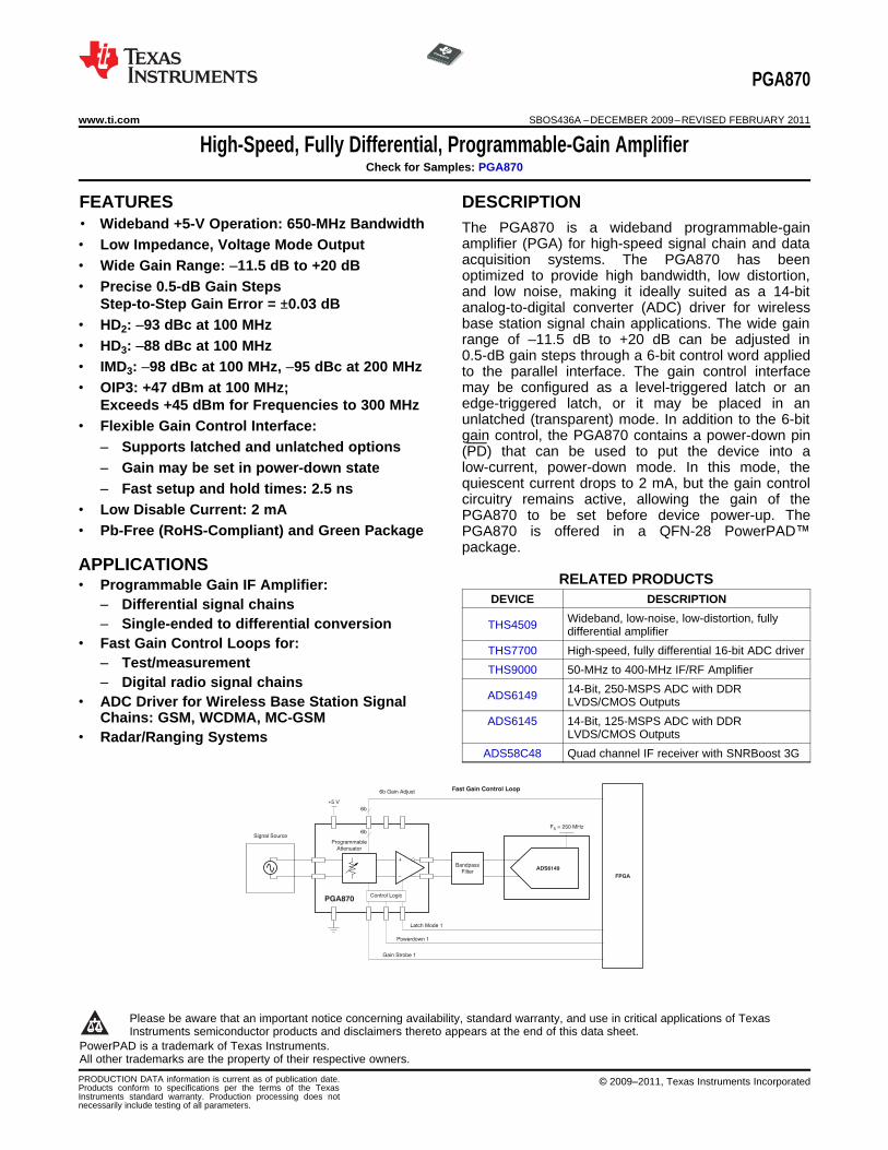
Programmable
Attenuator
Control LogicPGA870
6b
6bSignal Source
+5 V
Bandpass
FilterADS6149
F = 250 MHzS
Powerdown 1
Latch Mode 1
Gain Strobe 1
FPGA
6b Gain Adjust Fast Gain Control Loop
PGA870
www.ti.com SBOS436A –DECEMBER 2009–REVISED FEBRUARY 2011
High-Speed, Fully Differential, Programmable-Gain AmplifierCheck for Samples: PGA870
1FEATURES DESCRIPTION23• Wideband +5-V Operation: 650-MHz Bandwidth The PGA870 is a wideband programmable-gain
amplifier (PGA) for high-speed signal chain and data• Low Impedance, Voltage Mode Outputacquisition systems. The PGA870 has been• Wide Gain Range: –11.5 dB to +20 dBoptimized to provide high bandwidth, low distortion,
• Precise 0.5-dB Gain Steps and low noise, making it ideally suited as a 14-bitStep-to-Step Gain Error = ±0.03 dB analog-to-digital converter (ADC) driver for wireless
base station signal chain applications. The wide gain• HD2: –93 dBc at 100 MHzrange of –11.5 dB to +20 dB can be adjusted in• HD3: –88 dBc at 100 MHz0.5-dB gain steps through a 6-bit control word applied
• IMD3: –98 dBc at 100 MHz, –95 dBc at 200 MHz to the parallel interface. The gain control interfacemay be configured as a level-triggered latch or an• OIP3: +47 dBm at 100 MHz;edge-triggered latch, or it may be placed in anExceeds +45 dBm for Frequencies to 300 MHzunlatched (transparent) mode. In addition to the 6-bit• Flexible Gain Control Interface:gain control, the PGA870 contains a power-down pin
– Supports latched and unlatched options (PD) that can be used to put the device into alow-current, power-down mode. In this mode, the– Gain may be set in power-down statequiescent current drops to 2 mA, but the gain control– Fast setup and hold times: 2.5 nscircuitry remains active, allowing the gain of the
• Low Disable Current: 2 mA PGA870 to be set before device power-up. The• Pb-Free (RoHS-Compliant) and Green Package PGA870 is offered in a QFN-28 PowerPAD™
package.APPLICATIONS
RELATED PRODUCTS• Programmable Gain IF Amplifier:DEVICE DESCRIPTION– Differential signal chains
Wideband, low-noise, low-distortion, fully– Single-ended to differential conversion THS4509 differential amplifier• Fast Gain Control Loops for: THS7700 High-speed, fully differential 16-bit ADC driver
– Test/measurement THS9000 50-MHz to 400-MHz IF/RF Amplifier– Digital radio signal chains 14-Bit, 250-MSPS ADC with DDRADS6149 LVDS/CMOS Outputs• ADC Driver for Wireless Base Station SignalChains: GSM, WCDMA, MC-GSM ADS6145 14-Bit, 125-MSPS ADC with DDR
LVDS/CMOS Outputs• Radar/Ranging SystemsADS58C48 Quad channel IF receiver with SNRBoost 3G
1
Please be aware that an important notice concerning availability, standard warranty, and use in critical applications of TexasInstruments semiconductor products and disclaimers thereto appears at the end of this data sheet.
2PowerPAD is a trademark of Texas Instruments.3All other trademarks are the property of their respective owners.
PRODUCTION DATA information is current as of publication date. © 2009–2011, Texas Instruments IncorporatedProducts conform to specifications per the terms of the TexasInstruments standard warranty. Production processing does notnecessarily include testing of all parameters.
PGA870
SBOS436A –DECEMBER 2009–REVISED FEBRUARY 2011 www.ti.com
This integrated circuit can be damaged by ESD. Texas Instruments recommends that all integrated circuits be handled withappropriate precautions. Failure to observe proper handling and installation procedures can cause damage.
ESD damage can range from subtle performance degradation to complete device failure. Precision integrated circuits may be moresusceptible to damage because very small parametric changes could cause the device not to meet its published specifications.
ORDERING INFORMATION (1)
SPECIFIEDPACKAGE TEMPERATURE PACKAGE ORDERING TRANSPORT MEDIA,
PRODUCT PACKAGE-LEAD DESIGNATOR RANGE MARKING NUMBER QUANTITY
PGA870 PGA870IRHDT Tape and Reel, 250PGA870 QFN-28 RHD –40°C to +85°C
PGA870 PGA870IRHDR Tape and Reel, 3000
(1) For the most current package and ordering information see the Package Option Addendum at the end of this document, or see the TIweb site at www.ti.com.
ABSOLUTE MAXIMUM RATINGS (1)
Over operating free-air temperature range, unless otherwise noted.PGA870 UNIT
Power supply 6 V
Internal power dissipation See Thermal Characteristics
Input voltage range VS V
Storage temperature range –65 to +150 °C
Maximum junction temperature (TJ) +150 °C
Maximum junction temperature (TJ), continuous operation, long-term reliability +140 °C
Human body model (HBM) 2000 V
ESD rating Charged device model (CDM) 1000 V
Machine model (MM) 200 V
(1) Stresses above these ratings may cause permanent damage. Exposure to absolute maximum conditions for extended periods maydegrade device reliability. These are stress ratings only, and functional operation of the device at these or any other conditions beyondthose specified is not supported.
DISSIPATION RATINGS (1)
POWER RATING (2)
(TJ= +125°C)
PACKAGE θJP(°C/W) θJA(°C/W) TA= +25°C TA= +85°CQFN-28 4.1 35 2.9 W 0.87 W
(1) These data were taken with the JEDEC High-K test PCB. For the JEDEC low-K test PCB, θJA is 350°C/W.(2) Power rating is determined with a junction temperature of +125°C. This is the point where distortion starts to substantially increase and
long-term reliability starts to be reduced. Thermal management of the final printed circuit board should strive to keep the junctiontemperature at or below +125° C for best performance and reliability.
2 © 2009–2011, Texas Instruments Incorporated
Product Folder Link(s): PGA870
PGA870
www.ti.com SBOS436A –DECEMBER 2009–REVISED FEBRUARY 2011
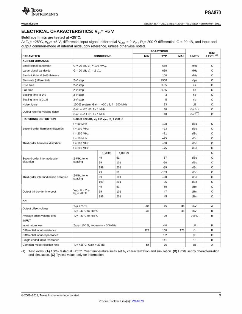
ELECTRICAL CHARACTERISTICS: VS+= +5 VBoldface limits are tested at +25°C.At TA= +25°C, VS+= +5 V, differential input signal, differential VOUT = 2 VPP, RL= 200 Ω differential, G = 20 dB, and input andoutput common-mode at internal midsupply reference, unless otherwise noted.
PGA870IRHDTEST
PARAMETER CONDITIONS MIN TYP MAX UNITS LEVEL (1)
AC PERFORMANCE
Small-signal bandwidth G = 20 dB, VO = 100 mVPP 650 MHz C
Large-signal bandwidth G = 20 dB, VO = 2 VPP 650 MHz C
Bandwidth for 0.1-dB flatness 100 MHz C
Slew rate (differential) 2-V step 2900 V/µs C
Rise time 2-V step 0.55 ns C
Fall time 2-V step 0.55 ns C
Settling time to 1% 2-V step 3 ns C
Settling time to 0.1% 2-V step 5 ns C
Noise figure 150-Ω system, Gain = +20 dB, f = 100 MHz 13 dB C
Gain = +20 dB, f > 1 MHz 30 nV/√Hz COutput-referred voltage noise
Gain = –11 dB, f > 1 MHz 40 nV/√Hz C
HARMONIC DISTORTION Gain = +20 dB, VO = 2 VPP, RL = 200 Ω
f = 50 MHz –108 dBc C
Second-order harmonic distortion f = 100 MHz –93 dBc C
f = 200 MHz –71 dBc C
f = 50 MHz –95 dBc C
Third-order harmonic distortion f = 100 MHz –88 dBc C
f = 200 MHz –75 dBc C
f1(MHz) f2(MHz) C
49 51 -87 dBc CSecond-order intermodulation 2-MHz tonedistortion spacing 99 101 -90 dBc C
199 201 -89 dBc C
49 51 -103 dBc C2-MHz toneThird-order intermodulation distortion 99 101 –98 dBc Cspacing
199 201 –95 dBc C
49 51 50 dBm CVOUT = 2 VPP,Output third-order intercept 99 101 47 dBm CRL = 200 Ω
199 201 45 dBm C
DC
TA= +25°C –30 ±5 30 mV AOutput offset voltage
TA= –40°C to +85°C –35 35 mV B
Average offset voltage drift TA= –40°C to +85°C 20 μV/°C B
INPUT
Input return loss ZSYS= 150 Ω, frequency < 300MHz -40 dB B
Differential input resistance 129 150 173 Ω B
Differential input capacitance 1.2 pF C
Single-ended input resistance 141 Ω B
Common-mode rejection ratio TA= +25°C, Gain = 20 dB 54 76 dB A
(1) Test levels: (A) 100% tested at +25°C. Over temperature limits set by characterization and simulation. (B) Limits set by characterizationand simulation. (C) Typical value; only for information.
© 2009–2011, Texas Instruments Incorporated 3
Product Folder Link(s): PGA870
PGA870
SBOS436A –DECEMBER 2009–REVISED FEBRUARY 2011 www.ti.com
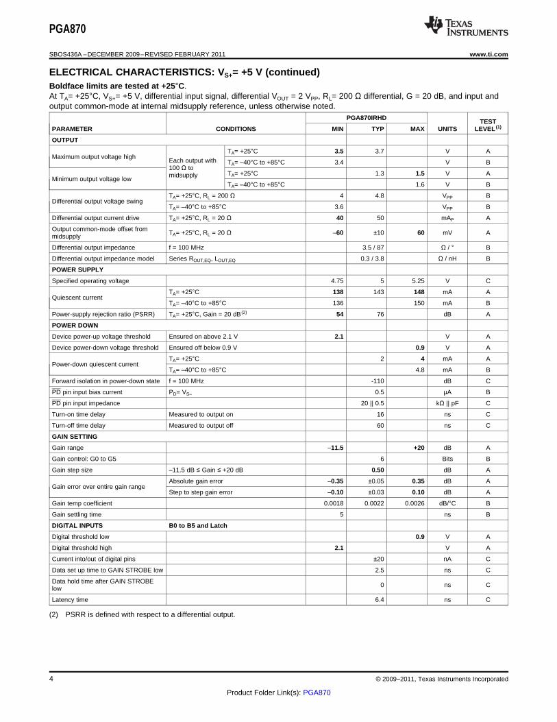
ELECTRICAL CHARACTERISTICS: VS+= +5 V (continued)Boldface limits are tested at +25°C.At TA= +25°C, VS+= +5 V, differential input signal, differential VOUT = 2 VPP, RL= 200 Ω differential, G = 20 dB, and input andoutput common-mode at internal midsupply reference, unless otherwise noted.
PGA870IRHDTEST
PARAMETER CONDITIONS MIN TYP MAX UNITS LEVEL (1)
OUTPUT
TA= +25°C 3.5 3.7 V AMaximum output voltage high
Each output with TA= –40°C to +85°C 3.4 V B100 Ω to
TA= +25°C 1.3 1.5 V AmidsupplyMinimum output voltage low
TA= –40°C to +85°C 1.6 V B
TA= +25°C, RL = 200 Ω 4 4.8 VPP BDifferential output voltage swing
TA= –40°C to +85°C 3.6 VPP B
Differential output current drive TA= +25°C, RL = 20 Ω 40 50 mAP A
Output common-mode offset from TA= +25°C, RL = 20 Ω –60 ±10 60 mV Amidsupply
Differential output impedance f = 100 MHz 3.5 / 87 Ω / ° B
Differential output impedance model Series ROUT,EQ, LOUT,EQ 0.3 / 3.8 Ω / nH B
POWER SUPPLY
Specified operating voltage 4.75 5 5.25 V C
TA= +25°C 138 143 148 mA AQuiescent current
TA= –40°C to +85°C 136 150 mA B
Power-supply rejection ratio (PSRR) TA= +25°C, Gain = 20 dB (2) 54 76 dB A
POWER DOWN
Device power-up voltage threshold Ensured on above 2.1 V 2.1 V A
Device power-down voltage threshold Ensured off below 0.9 V 0.9 V A
TA= +25°C 2 4 mA APower-down quiescent current
TA= –40°C to +85°C 4.8 mA B
Forward isolation in power-down state f = 100 MHz -110 dB C
PD pin input bias current PD= VS– 0.5 μA B
PD pin input impedance 20 || 0.5 kΩ || pF C
Turn-on time delay Measured to output on 16 ns C
Turn-off time delay Measured to output off 60 ns C
GAIN SETTING
Gain range –11.5 +20 dB A
Gain control: G0 to G5 6 Bits B
Gain step size –11.5 dB ≤ Gain ≤ +20 dB 0.50 dB A
Absolute gain error –0.35 ±0.05 0.35 dB AGain error over entire gain range
Step to step gain error –0.10 ±0.03 0.10 dB A
Gain temp coefficient 0.0018 0.0022 0.0026 dB/°C B
Gain settling time 5 ns B
DIGITAL INPUTS B0 to B5 and Latch
Digital threshold low 0.9 V A
Digital threshold high 2.1 V A
Current into/out of digital pins ±20 nA C
Data set up time to GAIN STROBE low 2.5 ns C
Data hold time after GAIN STROBE 0 ns Clow
Latency time 6.4 ns C
(2) PSRR is defined with respect to a differential output.
4 © 2009–2011, Texas Instruments Incorporated
Product Folder Link(s): PGA870
LATCH MODE
(MS
B)
B5
VS+
IN+
B3
VMID2
VS
+
IN-
B2
VS+
B1
GAIN STROBE
B0
GND
VS+
OUT+
GND
OUT-
VS+
GND
1
2
3
4
5
6
7
21
20
19
18
17
16
15
13
14
12
11
108
22
23
24
25
26
27
28
B4
VM
ID1
GN
D
VS
+
GN
D
GN
D
GN
D
PD
9
PowerPADä
PGA870
www.ti.com SBOS436A –DECEMBER 2009–REVISED FEBRUARY 2011
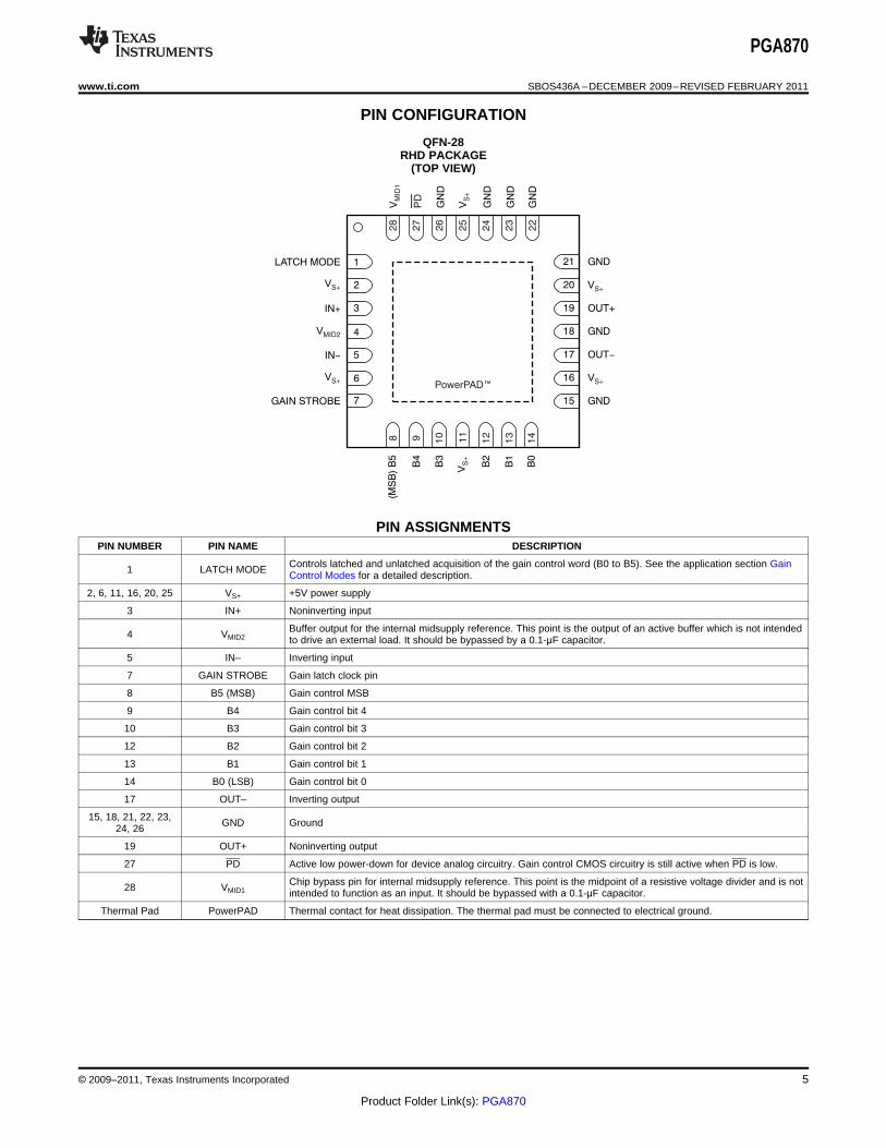
PIN CONFIGURATION
QFN-28RHD PACKAGE
(TOP VIEW)
PIN ASSIGNMENTSPIN NUMBER PIN NAME DESCRIPTION
Controls latched and unlatched acquisition of the gain control word (B0 to B5). See the application section Gain1 LATCH MODE Control Modes for a detailed description.
2, 6, 11, 16, 20, 25 VS+ +5V power supply
3 IN+ Noninverting input
Buffer output for the internal midsupply reference. This point is the output of an active buffer which is not intended4 VMID2 to drive an external load. It should be bypassed by a 0.1-μF capacitor.
5 IN– Inverting input
7 GAIN STROBE Gain latch clock pin
8 B5 (MSB) Gain control MSB
9 B4 Gain control bit 4
10 B3 Gain control bit 3
12 B2 Gain control bit 2
13 B1 Gain control bit 1
14 B0 (LSB) Gain control bit 0
17 OUT– Inverting output
15, 18, 21, 22, 23, GND Ground24, 26
19 OUT+ Noninverting output
27 PD Active low power-down for device analog circuitry. Gain control CMOS circuitry is still active when PD is low.
Chip bypass pin for internal midsupply reference. This point is the midpoint of a resistive voltage divider and is not28 VMID1 intended to function as an input. It should be bypassed with a 0.1-μF capacitor.
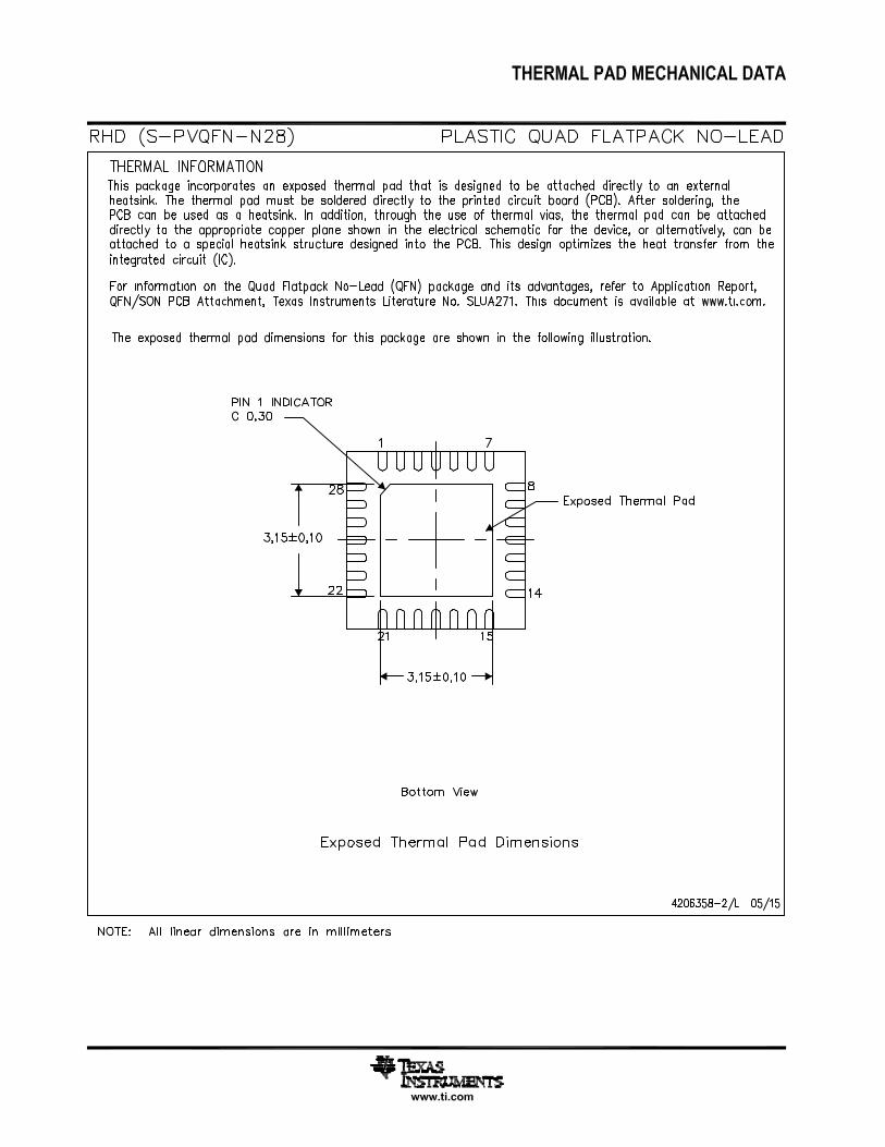
Thermal Pad PowerPAD Thermal contact for heat dissipation. The thermal pad must be connected to electrical ground.
© 2009–2011, Texas Instruments Incorporated 5
Product Folder Link(s): PGA870
10
5
0
5
10
15
-
-
-
Ga
in (
dB
)
10 100 1000
Frequency (MHz)
Gain = +5 dB
Gain = 11.5 dB-
Gain Adjusted in 0.5-dB Steps
V = 200 mVOUT PP
25
20
15
10
5
0
Ga
in (
dB
)
10 100 1000
Frequency (MHz)
Gain = +20 dB
Gain = +5.5 dB
Gain Adjusted in 0.5-dB Steps
V = 200 mVOUT PP
30
25
20
15
10
5
0
5
10
15
20
-
-
-
-
Ga
in (
dB
)
10 100 1000
Frequency (MHz)
Gain = 20 dB
Gain = 10 dB
Gain = 0 dB
Gain = 6 dB-
Differential Input
V = 2 VOUT PP
30
25
20
15
10
5
0
5
10
15
20-
-
-
-
Ga
in (
dB
)
10 100 1000
Frequency (MHz)
Gain = 20 dB
Gain = 10 dB
Gain = 0 dB
Gain = 6 dB-
Single-Ended Input
V = 2 VOUT PP
10 100 1000
Frequency (MHz)
25
20
15
10
5
0
Gain
(dB
)
C = 820 pFL
C = 470 pFL
C = 94 pFL
C = 44 pFL
C =
10 pFL
C =
20 pFL
C =
16 pFL
PGA870
ROS
VOUTROS
CL
CL
100
10
1
R(
)W
OS
1 10 100 1000
Capacitive Load (pF)
PGA870
ROS
VOUTROS
CL
CL
PGA870
SBOS436A –DECEMBER 2009–REVISED FEBRUARY 2011 www.ti.com
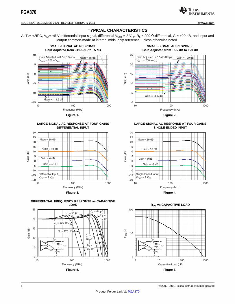
TYPICAL CHARACTERISTICSAt TA= +25°C, VS+= +5 V, differential input signal, differential VOUT = 2 VPP, RL = 200 Ω differential, G = +20 dB, and input and
output common-mode at internal midsupply reference, unless otherwise noted.
SMALL-SIGNAL AC RESPONSE SMALL-SIGNAL AC RESPONSEGain Adjusted from –11.5 dB to +5 dB Gain Adjusted from +5.5 dB to +20 dB
Figure 1. Figure 2.
LARGE-SIGNAL AC RESPONSE AT FOUR GAINS LARGE-SIGNAL AC RESPONSE AT FOUR GAINSDIFFERENTIAL INPUT SINGLE-ENDED INPUT
Figure 3. Figure 4.
DIFFERENTIAL FREQUENCY RESPONSE vs CAPACITIVELOAD ROS vs CAPACITIVE LOAD
Figure 5. Figure 6.
6 © 2009–2011, Texas Instruments Incorporated
Product Folder Link(s): PGA870
-12-10 -8 -6 -4 -2 0 2 4 6 8 10 12 14 16 18 20
Gain Setting
25
20
15
10
5
0
5
10
15
-
-
-
Gain
(dB
)
50 MHz
100 MHz
200 MHz
-12-10 -8 -6 -4 -2 0 2 4 6 8 10 12 14 16 18 20
Gain Setting
0.15
0.10
0.05
0
0.05
15
0.
-
-
-
-
0.10
0.
20
Ga
in E
rro
r (d
B)
-40 C°
+25 C°
+85 C°
-12-10 -8 -6 -4 -2 0 2 4 6 8 10 12 14 16 18 20
Gain Setting
0.04
0.02
0
0.02
0.04
0.06
0.08
-
-
-
-
Gain
Err
or
(dB
)
50 MHz
100 MHz
200 MHz
4.0
3.5
3.0
2.5
2.0
1.5
1.0
0.5
0
0.5
1.0
-
-
Ga
in C
on
tro
l (V
)
0 100 200 300 400 500
Time (ns)
1.5
1.0
0.5
0
-0.5
-1.0
-1.5
Am
plifie
r Ou
tpu
t (V)
Gain Control Gain Code = 111111
Gain Code = 000000Amplifier
Output
2.5
2.0
1.5
1.0
0.5
0 1.0
0.5
0
0.5
1.0
-
-
Ga
in C
on
tro
l, G
ain
Str
ob
e (
V)
Am
plifie
r Outp
ut (V
)
Time (50 ns/div)
Gain Code =
111111
Gain Code =
000000
Gain Strobe2.5
2.0
1.5
1.0
0.5
0 1.0
0.5
0
0.5
1.0
-
-
Ga
in C
on
tro
l, G
ain
Str
obe
(V
)
Am
plifie
r Outp
ut (V
)
Time (50 ns/div)
Gain Code = 111111
Gain Code =
000000
Gain
Strobe
PGA870
www.ti.com SBOS436A –DECEMBER 2009–REVISED FEBRUARY 2011
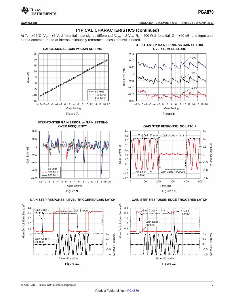
TYPICAL CHARACTERISTICS (continued)At TA= +25°C, VS+= +5 V, differential input signal, differential VOUT = 2 VPP, RL = 200 Ω differential, G = +20 dB, and input andoutput common-mode at internal midsupply reference, unless otherwise noted.
STEP-TO-STEP GAIN ERROR vs GAIN SETTINGLARGE-SIGNAL GAIN vs GAIN SETTING OVER TEMPERATURE
Figure 7. Figure 8.
STEP-TO-STEP GAIN ERROR vs GAIN SETTINGOVER FREQUENCY GAIN STEP RESPONSE: NO LATCH
Figure 9. Figure 10.
GAIN STEP RESPONSE: LEVEL-TRIGGERED GAIN LATCH GAIN STEP RESPONSE: EDGE-TRIGGERED LATCH
Figure 11. Figure 12.
© 2009–2011, Texas Instruments Incorporated 7
Product Folder Link(s): PGA870
-
-
-
-
-
-
-
70
75
80
85
90
95
100
IMD
(dB
c)
2
50 100 150 200 250 300
Frequency (MHz)
R = 100 WL
R = 200
R = 500
R = 1 k
L
L
L
W
W
W
V = 2 VOUT PP
F = 2 MHzD
Gain = +10 dB
-80
82
84
86
88
90
92
94
96
98
100
102
104
106
108
110
-
-
-
-
-
-
-
-
-
-
-
-
-
-
-
IMD
(dB
c)
3
50 100 150 200 250 300
Frequency (MHz)
R = 100 WL
R = 200
R = 500
R = 1 k
L
L
L
W
W
W
Dashed lines: Gain = 6 dB-
Solid lines: Gain = +10 dB
V = 2 VOUT PP
F = 2 MHzD
-
-
-
-
-
-
-
70
75
80
85
90
95
100
IMD
(dB
c)
2
50 100 150 200 250 300
Frequency (MHz)
R = 100 WL
R = 200
R = 500
R = 1 k
L
L
L
W
W
W
V = 2 VOUT PP
F = 2 MHzD
Gain = +20 dB
-80
82
84
86
88
90
92
94
96
98
100
102
104
106
108
110
-
-
-
-
-
-
-
-
-
-
-
-
-
-
-
IMD
(dB
c)
3
50 100 150 200 250 300
Frequency (MHz)
R = 100 WL
R = 200
R = 500
R = 1 k
L
L
L
W
W
W
Dashed lines: Gain = 0 dB
Solid lines: Gain = +20 dB
V = 2 VOUT PP
F = 2 MHzD
OIP
(dB
m)
3
50 100 150 200 250 300
Frequency (MHz)
V = 2 V
R = 200OUT PP
L W
50
48
46
44
42
40
38
36
Gain = +20 dB
Gain = +10 dB
Gain = 0 dB
Gain = dB-6
PGA870
SBOS436A –DECEMBER 2009–REVISED FEBRUARY 2011 www.ti.com
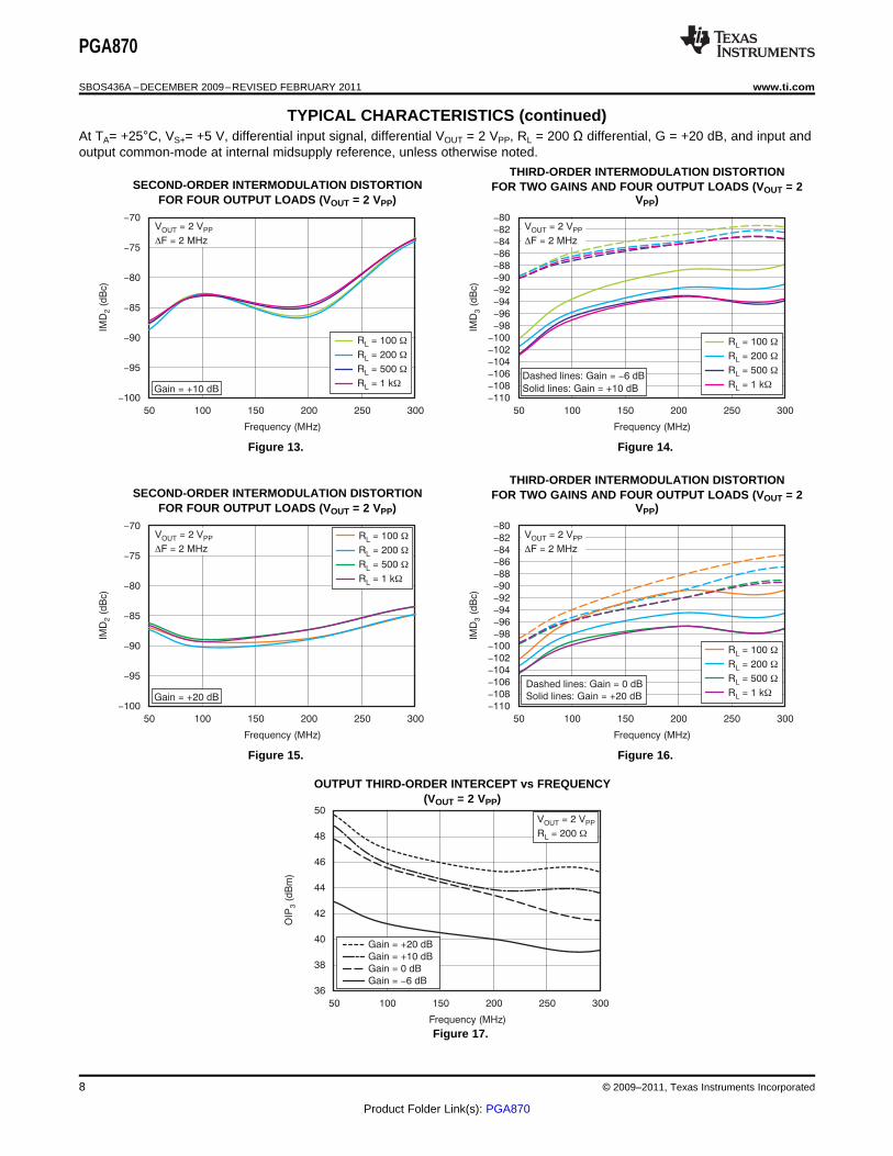
TYPICAL CHARACTERISTICS (continued)At TA= +25°C, VS+= +5 V, differential input signal, differential VOUT = 2 VPP, RL = 200 Ω differential, G = +20 dB, and input andoutput common-mode at internal midsupply reference, unless otherwise noted.
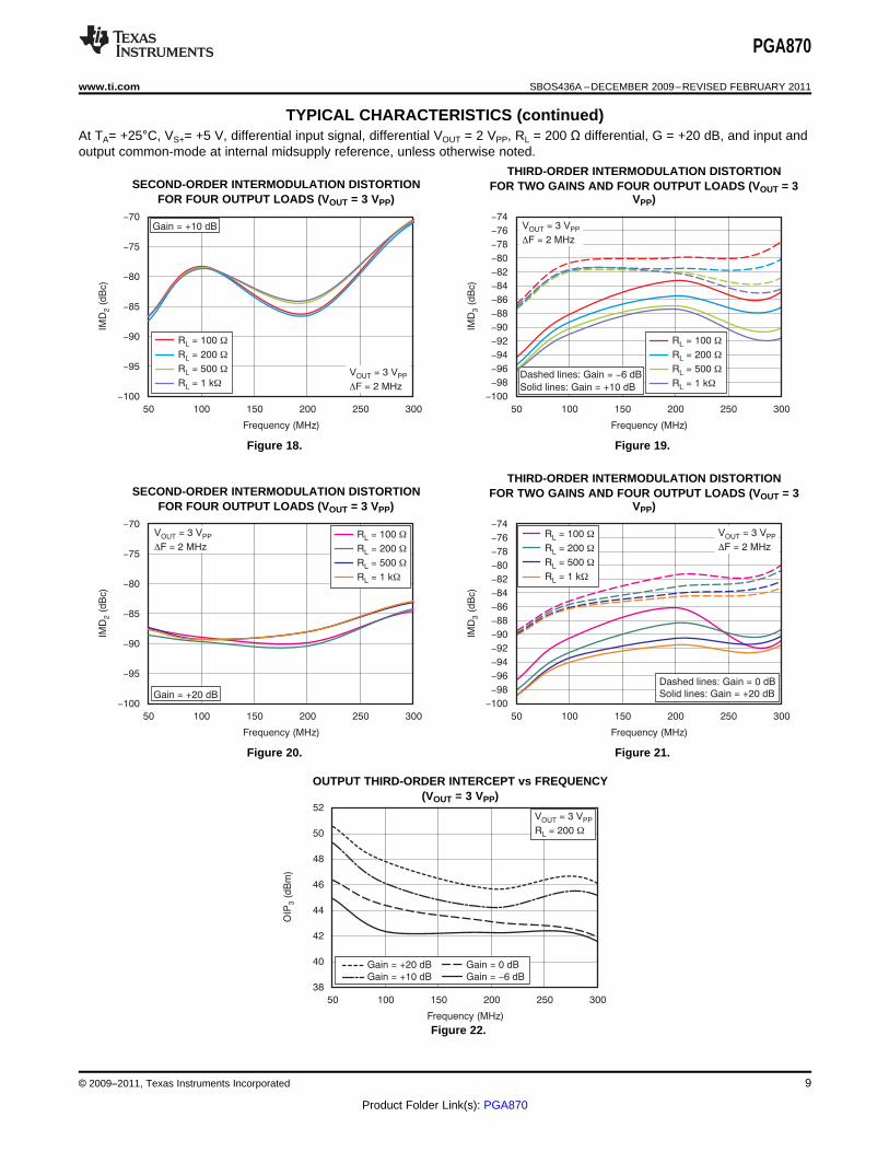
THIRD-ORDER INTERMODULATION DISTORTIONSECOND-ORDER INTERMODULATION DISTORTION FOR TWO GAINS AND FOUR OUTPUT LOADS (VOUT = 2
FOR FOUR OUTPUT LOADS (VOUT = 2 VPP) VPP)
Figure 13. Figure 14.
THIRD-ORDER INTERMODULATION DISTORTIONSECOND-ORDER INTERMODULATION DISTORTION FOR TWO GAINS AND FOUR OUTPUT LOADS (VOUT = 2
FOR FOUR OUTPUT LOADS (VOUT = 2 VPP) VPP)
Figure 15. Figure 16.
OUTPUT THIRD-ORDER INTERCEPT vs FREQUENCY(VOUT = 2 VPP)
Figure 17.
8 © 2009–2011, Texas Instruments Incorporated
Product Folder Link(s): PGA870
-
-
-
-
-
-
-
70
75
80
85
90
95
100
IMD
(dB
c)
2
50 100 150 200 250 300
Frequency (MHz)
R = 100 WL
R = 200
R = 500
R = 1 k
L
L
L
W
W
W
V = 3 VOUT PP
F = 2 MHzD
Gain = +10 dB-74
76
78
80
82
84
86
88
90
92
94
96
98
100
-
-
-
-
-
-
-
-
-
-
-
-
-
IMD
(dB
c)
3
50 100 150 200 250 300
Frequency (MHz)
R = 100 WL
R = 200
R = 500
R = 1 k
L
L
L
W
W
W
Dashed lines: Gain = 6 dB-
Solid lines: Gain = +10 dB
V = 3 VOUT PP
F = 2 MHzD
70
75
80
85
90
95
100
-
-
-
-
-
-
-
IMD
(dB
c)
2
50 100 150 200 250 300
Frequency (MHz)
R = 100 WL
R = 200
R = 500
R = 1 k
L
L
L
W
W
W
V = 3 VOUT PP
F = 2 MHzD
Gain = +20 dB
-74
76
78
80
82
84
86
88
90
92
94
96
98
100
-
-
-
-
-
-
-
-
-
-
-
-
-
IMD
(dB
c)
3
50 100 150 200 250 300
Frequency (MHz)
R = 100 WL
R = 200
R = 500
R = 1 k
L
L
L
W
W
W
Dashed lines: Gain = 0 dB
Solid lines: Gain = +20 dB
V = 3 VOUT PP
F = 2 MHzD
OIP
(dB
m)
3
50 100 150 200 250 300
Frequency (MHz)
V = 3 V
R = 200OUT PP
L W
52
50
48
46
44
42
40
38
Gain = +20 dB
Gain = +10 dB
Gain = 0 dB
Gain = 6 dB-
PGA870
www.ti.com SBOS436A –DECEMBER 2009–REVISED FEBRUARY 2011
TYPICAL CHARACTERISTICS (continued)At TA= +25°C, VS+= +5 V, differential input signal, differential VOUT = 2 VPP, RL = 200 Ω differential, G = +20 dB, and input andoutput common-mode at internal midsupply reference, unless otherwise noted.
THIRD-ORDER INTERMODULATION DISTORTIONSECOND-ORDER INTERMODULATION DISTORTION FOR TWO GAINS AND FOUR OUTPUT LOADS (VOUT = 3
FOR FOUR OUTPUT LOADS (VOUT = 3 VPP) VPP)
Figure 18. Figure 19.
THIRD-ORDER INTERMODULATION DISTORTIONSECOND-ORDER INTERMODULATION DISTORTION FOR TWO GAINS AND FOUR OUTPUT LOADS (VOUT = 3
FOR FOUR OUTPUT LOADS (VOUT = 3 VPP) VPP)
Figure 20. Figure 21.
OUTPUT THIRD-ORDER INTERCEPT vs FREQUENCY(VOUT = 3 VPP)
Figure 22.
© 2009–2011, Texas Instruments Incorporated 9
Product Folder Link(s): PGA870
-55
60
65
70
75
80
85
90
95
100
105
110
-
-
-
-
-
-
-
-
-
-
-
-45
50
55
60
65
70
75
80
85
90
95
100
-
-
-
-
-
-
-
-
-
-
-
Se
co
nd
-Ord
er
Ha
rmo
nic
Dis
tort
ion
(d
Bc) T
hird
-Ord
er H
arm
on
ic D
isto
rtion
(dB
c)
50 100 150 200 250 300
Frequency (MHz)
0
Gain = 6 dB-
Gain = 0 dB
Dashed lines: 2nd Harmonic
Solid lines: 3rd Harmonic
V = 2 V
R = 100OUT PP
L W
Gain = +10 dB
Gain = +20 dB
-55
60
65
70
75
80
85
90
95
100
105
110
-
-
-
-
-
-
-
-
-
-
-
-45
50
55
60
65
70
75
80
85
90
95
100
-
-
-
-
-
-
-
-
-
-
-
Se
co
nd
-Ord
er
Ha
rmo
nic
Dis
tort
ion
(d
Bc) T
hird
-Ord
er H
arm
on
ic D
isto
rtion
(dB
c)
50 100 150 200 250 300
Frequency (MHz)
0
Gain = 6 dB-
Gain = 0 dB
Dashed lines: 2nd Harmonic
Solid lines: 3rd Harmonic
V = 2 V
R = 200OUT PP
L W
Gain = +10 dB
Gain = +20 dB
-55
60
65
70
75
80
85
90
95
100
105
110
-
-
-
-
-
-
-
-
-
-
-
-45
50
55
60
65
70
75
80
85
90
95
100
-
-
-
-
-
-
-
-
-
-
-
Se
co
nd
-Ord
er
Ha
rmo
nic
Dis
tort
ion
(d
Bc) T
hird
-Ord
er H
arm
on
ic D
isto
rtion
(dB
c)
50 100 150 200 250 300
Frequency (MHz)
0
Gain = 6 dB-
Gain = 0 dB
Dashed lines: 2nd Harmonic
Solid lines: 3rd Harmonic
V = 2 V
R = 500OUT PP
L W
Gain = +10 dB
Gain = +20 dB
-55
60
65
70
75
80
85
90
95
100
105
110
-
-
-
-
-
-
-
-
-
-
-
-45
50
55
60
65
70
75
80
85
90
95
100
-
-
-
-
-
-
-
-
-
-
-
Se
co
nd
-Ord
er
Ha
rmo
nic
Dis
tort
ion
(d
Bc) T
hird
-Ord
er H
arm
on
ic D
isto
rtion
(dB
c)
50 100 150 200 250 300
Frequency (MHz)
0
Dashed lines: 2nd Harmonic
Solid lines: 3rd Harmonic
V = 2 V
R = 1 kOUT PP
L W
Gain = 6 dB-
Gain = 0 dB
Gain = +10 dB
Gain = +20 dB
PGA870
SBOS436A –DECEMBER 2009–REVISED FEBRUARY 2011 www.ti.com
TYPICAL CHARACTERISTICS (continued)At TA= +25°C, VS+= +5 V, differential input signal, differential VOUT = 2 VPP, RL = 200 Ω differential, G = +20 dB, and input andoutput common-mode at internal midsupply reference, unless otherwise noted.
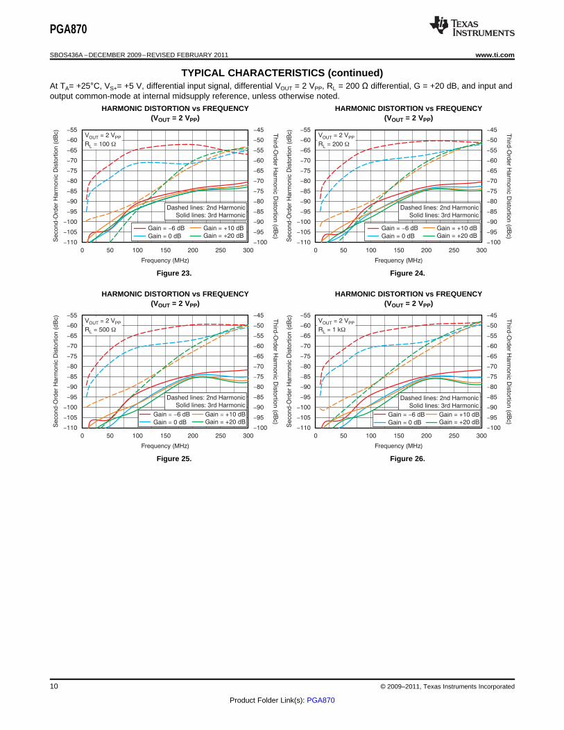
HARMONIC DISTORTION vs FREQUENCY HARMONIC DISTORTION vs FREQUENCY(VOUT = 2 VPP) (VOUT = 2 VPP)
Figure 23. Figure 24.
HARMONIC DISTORTION vs FREQUENCY HARMONIC DISTORTION vs FREQUENCY(VOUT = 2 VPP) (VOUT = 2 VPP)
Figure 25. Figure 26.
10 © 2009–2011, Texas Instruments Incorporated
Product Folder Link(s): PGA870
-55
60
65
70
75
80
85
90
95
100
105
110
-
-
-
-
-
-
-
-
-
-
-
-40
45
50
55
60
65
70
75
80
85
90
95
-
-
-
-
-
-
-
-
-
-
-
Se
co
nd
-Ord
er
Ha
rmo
nic
Dis
tort
ion
(d
Bc) T
hird
-Ord
er H
arm
on
ic D
isto
rtion
(dB
c)
50 100 150 200 250 300
Frequency (MHz)
0
Gain = 6 dB-
Gain = 0 dB
Dashed lines: 2nd Harmonic
Solid lines: 3rd Harmonic
V = 3 V
R = 100OUT PP
L W
Gain = +10 dB
Gain = +20 dB
-55
60
65
70
75
80
85
90
95
100
105
110
-
-
-
-
-
-
-
-
-
-
-
-40
45
50
55
60
65
70
75
80
85
90
95
-
-
-
-
-
-
-
-
-
-
-
Se
co
nd
-Ord
er
Ha
rmo
nic
Dis
tort
ion
(d
Bc) T
hird
-Ord
er H
arm
on
ic D
isto
rtion
(dB
c)
50 100 150 200 250 300
Frequency (MHz)
0
Gain = 6 dB-
Gain = 0 dB
Dashed lines: 2nd Harmonic
Solid lines: 3rd Harmonic
V = 3 V
R = 200OUT PP
L W
Gain = +10 dB
Gain = +20 dB
-55
60
65
70
75
80
85
90
95
100
105
110
-
-
-
-
-
-
-
-
-
-
-
-40
45
50
55
60
65
70
75
80
85
90
95
-
-
-
-
-
-
-
-
-
-
-
Se
co
nd
-Ord
er
Ha
rmo
nic
Dis
tort
ion
(d
Bc) T
hird
-Ord
er H
arm
on
ic D
isto
rtion
(dB
c)
50 100 150 200 250 300
Frequency (MHz)
0
Gain = 6 dB-
Gain = 0 dB
Dashed lines: 2nd Harmonic
Solid lines: 3rd Harmonic
V = 3 V
R = 500OUT PP
L W
Gain = +10 dB
Gain = +20 dB
-55
60
65
70
75
80
85
90
95
100
105
110
-
-
-
-
-
-
-
-
-
-
-
-40
45
50
55
60
65
70
75
80
85
90
95
-
-
-
-
-
-
-
-
-
-
-
Se
co
nd
-Ord
er
Ha
rmo
nic
Dis
tort
ion
(d
Bc) T
hird
-Ord
er H
arm
on
ic D
isto
rtion
(dB
c)
50 100 150 200 250 300
Frequency (MHz)
0
Gain = 6 dB-
Gain = 0 dB
Dashed lines: 2nd Harmonic
Solid lines: 3rd Harmonic
V = 3 V
R = 1 kOUT PP
L W
Gain = +10 dB
Gain = +20 dB
PGA870
www.ti.com SBOS436A –DECEMBER 2009–REVISED FEBRUARY 2011
TYPICAL CHARACTERISTICS (continued)At TA= +25°C, VS+= +5 V, differential input signal, differential VOUT = 2 VPP, RL = 200 Ω differential, G = +20 dB, and input andoutput common-mode at internal midsupply reference, unless otherwise noted.
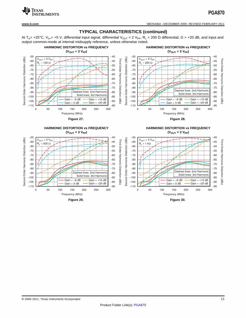
HARMONIC DISTORTION vs FREQUENCY HARMONIC DISTORTION vs FREQUENCY(VOUT = 3 VPP) (VOUT = 3 VPP)
Figure 27. Figure 28.
HARMONIC DISTORTION vs FREQUENCY HARMONIC DISTORTION vs FREQUENCY(VOUT = 3 VPP) (VOUT = 3 VPP)
Figure 29. Figure 30.
© 2009–2011, Texas Instruments Incorporated 11
Product Folder Link(s): PGA870
45
40
35
30
25
20
15
10
No
ise
Fig
ure
(d
B)
-12 -8 -4 0 4 8 12 16 222018141062-2-6-10
Gain (dB)
f = 100 MHz
R = 150SYS W
1000
100
10
Ou
tpu
t V
olta
ge
No
ise
(n
V/
)?H
z
10 100 1 k 10 k 100 k 1 M 10 M 100 M
Frequency (Hz)
Gain = +20 dB
Gain = 11.5 dB-
2.25
2.00
1.75
1.50
1.25
1.00
0.75
0.50
0.25
0
0.25-
1.5
1.2
0.9
0.6
0.3
0
0.3-
-
-
-
-
0.6
0.9
1.2
1.5
Dis
able
Sig
nal A
mplit
ude (
V)
Am
plifie
r Outp
ut (V
)
100 200 300 400 500
Time (ns)
Disable Signal
Amplifier Output
1.5
1.0
0.5
0
0.5
1.0
1.5
-
-
-
0.15
0.10
0.05
0
0.05
0.10
0.15
-
-
-
Larg
e-S
ignal D
iffe
rential O
utp
ut (V
) Sm
all-S
ignal D
iffere
ntia
l Outp
ut (V
)
0 5 10 15 20 25
Time (2.5 ns/div)
Gain = 20 dB, R = 200 WL
Right Scale
Left Scale
160
150
140
130
120
110
100
4
0
4
8
12
16
20-
-
-
-
-
Inp
ut
Imp
ed
an
ce
Ma
gn
itu
de
()
W Inp
ut Im
pe
da
nce
Ph
ase
()°
100 k 1 M 10 M 100 M 1 G
Frequency (Hz)
Magnitude
Phase
-
-
-
-
-
60
80
100
120
140
Fo
rwa
rd I
so
latio
n (
dB
)
0 100 200 300 400 500
Frequency (MHz)
PGA870
SBOS436A –DECEMBER 2009–REVISED FEBRUARY 2011 www.ti.com
TYPICAL CHARACTERISTICS (continued)At TA= +25°C, VS+= +5 V, differential input signal, differential VOUT = 2 VPP, RL = 200 Ω differential, G = +20 dB, and input andoutput common-mode at internal midsupply reference, unless otherwise noted.
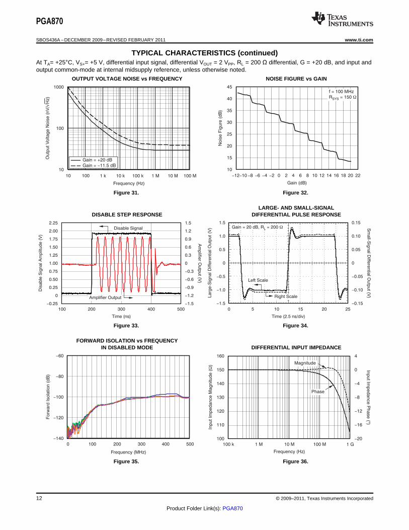
OUTPUT VOLTAGE NOISE vs FREQUENCY NOISE FIGURE vs GAIN
Figure 31. Figure 32.
LARGE- AND SMALL-SIGNALDISABLE STEP RESPONSE DIFFERENTIAL PULSE RESPONSE
Figure 33. Figure 34.
FORWARD ISOLATION vs FREQUENCYIN DISABLED MODE DIFFERENTIAL INPUT IMPEDANCE
Figure 35. Figure 36.
12 © 2009–2011, Texas Instruments Incorporated
Product Folder Link(s): PGA870
0
10
20
30
40
50
60-
-
-
-
-
-
Input R
etu
rn L
oss (
dB
)
100 M 1 G
Frequency (Hz)
Z = 150 WSYS
20 dB
10 dB
0 dB
6 dB-
0
5
10
15
20
25
30
35-
-
-
-
-
-
-
Inp
ut
Re
turn
Lo
ss (
dB
)
10 M 100 M 1 G
Frequency (Hz)
Z = 150 WSYS
20 dB
10 dB
0 dB
6 dB-
5.5
5.0
4.5
4.0
3.5
Diffe
ren
tia
l O
utp
ut
Sw
ing
(V
)
100 1 k 10 k
Differential Load Resistance, R ( )WLOAD
100
10
1
0.1
Ou
tpu
t Im
pe
da
nce
Ma
gn
itu
de
()
W
10 k 100 k 1 M 10 M 100 M 300 M
Frequency (Hz)
100
90
80
70
60
50
40
30
20
10
0
Outp
ut Im
pedance P
hase (
)°Magnitude
Phase
90
80
70
60
50
40
30
20
10
0
Pow
er-
Supply
Reje
ction R
atio (
dB
)
Com
mon-M
ode R
eje
ction R
atio (
dB
)
1 k 10 k 100 k 1 M 10 M 100 M 1 G
Frequency (Hz)
CMRR
PSRR
PGA870
www.ti.com SBOS436A –DECEMBER 2009–REVISED FEBRUARY 2011
TYPICAL CHARACTERISTICS (continued)At TA= +25°C, VS+= +5 V, differential input signal, differential VOUT = 2 VPP, RL = 200 Ω differential, G = +20 dB, and input andoutput common-mode at internal midsupply reference, unless otherwise noted.
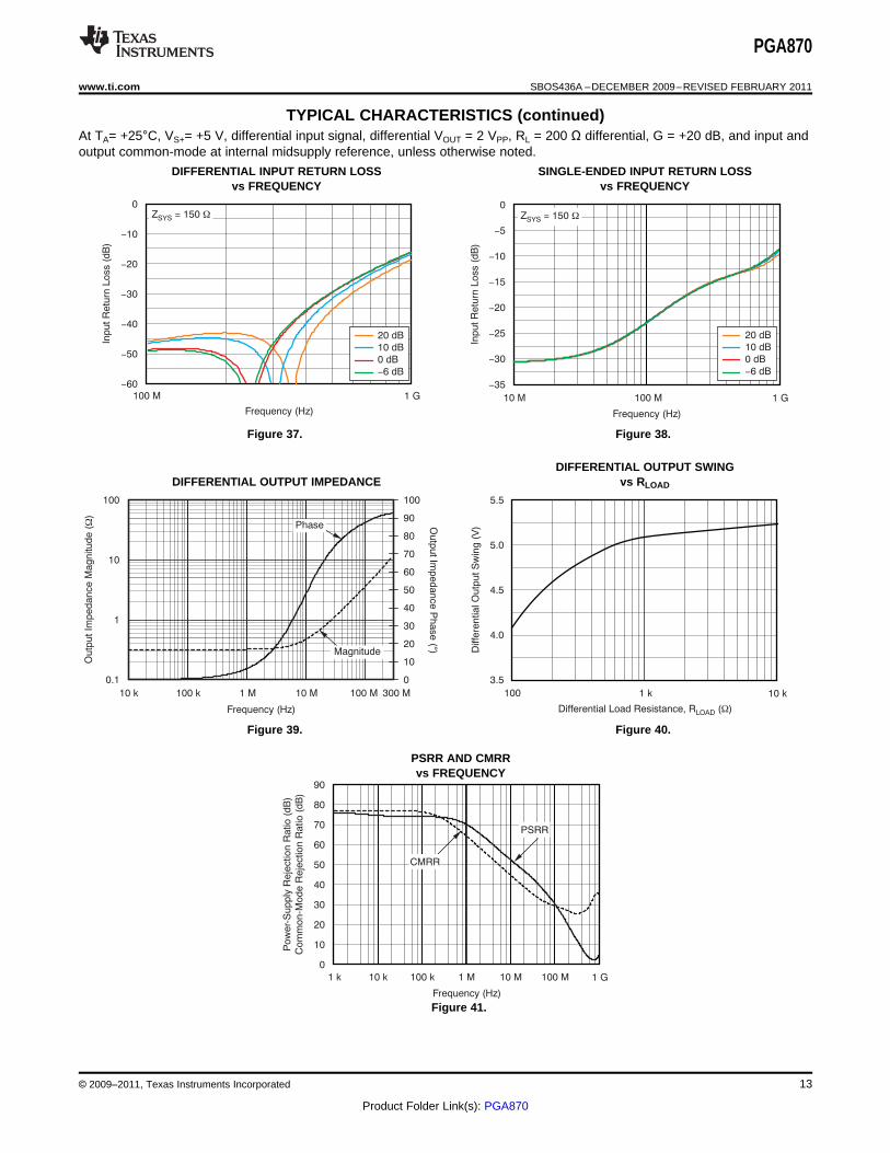
DIFFERENTIAL INPUT RETURN LOSS SINGLE-ENDED INPUT RETURN LOSSvs FREQUENCY vs FREQUENCY
Figure 37. Figure 38.
DIFFERENTIAL OUTPUT SWINGDIFFERENTIAL OUTPUT IMPEDANCE vs RLOAD
Figure 39. Figure 40.
PSRR AND CMRRvs FREQUENCY
Figure 41.
© 2009–2011, Texas Instruments Incorporated 13
Product Folder Link(s): PGA870
VS
Attenuator
IN-
VMID2
IN+
1
2
7
8
Buffered
MUX
Output
Amp
Gain ControlBIAS
Control
Gain
Strobe
Latch
Mode
B0
(LSB)
B1 B2 B3 B4 B5
(MSB)
Disable
OUT-
OUT+
PGA870
Gain = +20 dB
PGA870
SBOS436A –DECEMBER 2009–REVISED FEBRUARY 2011 www.ti.com
APPLICATION INFORMATION
Device Operation
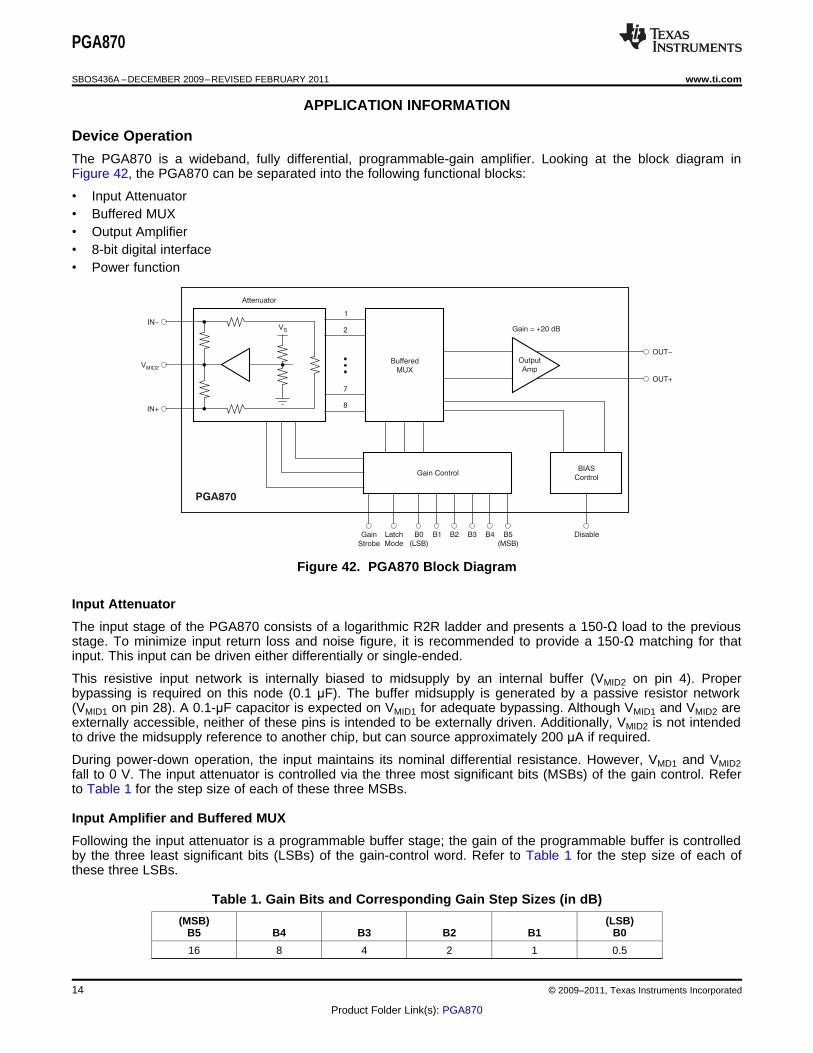
The PGA870 is a wideband, fully differential, programmable-gain amplifier. Looking at the block diagram inFigure 42, the PGA870 can be separated into the following functional blocks:
• Input Attenuator• Buffered MUX• Output Amplifier• 8-bit digital interface• Power function
Figure 42. PGA870 Block Diagram
Input Attenuator
The input stage of the PGA870 consists of a logarithmic R2R ladder and presents a 150-Ω load to the previousstage. To minimize input return loss and noise figure, it is recommended to provide a 150-Ω matching for thatinput. This input can be driven either differentially or single-ended.
This resistive input network is internally biased to midsupply by an internal buffer (VMID2 on pin 4). Properbypassing is required on this node (0.1 μF). The buffer midsupply is generated by a passive resistor network(VMID1 on pin 28). A 0.1-μF capacitor is expected on VMID1 for adequate bypassing. Although VMID1 and VMID2 areexternally accessible, neither of these pins is intended to be externally driven. Additionally, VMID2 is not intendedto drive the midsupply reference to another chip, but can source approximately 200 μA if required.
During power-down operation, the input maintains its nominal differential resistance. However, VMD1 and VMID2fall to 0 V. The input attenuator is controlled via the three most significant bits (MSBs) of the gain control. Referto Table 1 for the step size of each of these three MSBs.
Input Amplifier and Buffered MUX
Following the input attenuator is a programmable buffer stage; the gain of the programmable buffer is controlledby the three least significant bits (LSBs) of the gain-control word. Refer to Table 1 for the step size of each ofthese three LSBs.
Table 1. Gain Bits and Corresponding Gain Step Sizes (in dB)
(MSB) (LSB)B5 B4 B3 B2 B1 B0
16 8 4 2 1 0.5
14 © 2009–2011, Texas Instruments Incorporated
Product Folder Link(s): PGA870
PGA870
www.ti.com SBOS436A –DECEMBER 2009–REVISED FEBRUARY 2011
Output Amplifier
The PGA870 has a differential, voltage-mode output stage with a differential output resistance of approximately0.3 Ω and an inductive reactance equivalent to 3.8 nH. The common-mode output voltage has a nominal value ofVMID2. This output amplifier has a nominal gain of +20 dB.
The nominal load is 200 Ω, but the PGA870 can drive loads as low as 100 Ω with only minor changes to thedevice distortion.
The output pins go to a high-impedance state when the device is the power-down state (that is, when PD is low).
8-bit Digital Interface
The 8-bit digital interface is composed of six bits: three MSBs that control the input attenuation and three LSBsthat control the input amplifier and buffered MUX. For more information on this parallel interface, refer to the GainControl and Latch Modes section.
Power Function
The PGA870 features a low-power disabled state for the analog circuitry when the power-down (PD) pin is low.In the disabled state, the digital circuitry remains active, which allows the gain to be set before device power-up.There is no internal circuitry to provide a nominal bias to this pin. If this pin is to be left open, it must be biasedwith an external pull-up resistor.
Note that when the PGA870 is in this low-power mode, the gain can be programmed using the 8-bit digitalinterface, the output pins go to a high-impedance state, and the voltage on the midsupply pins biasing theattenuator (pin 4 and pin 28) goes to 0 V.
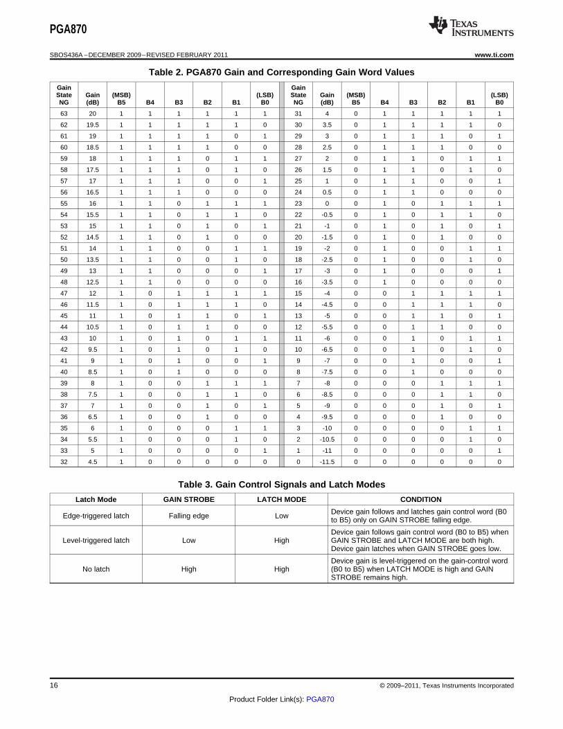
Gain Control and Latch Modes
The PGA870 has six bits of gain control (B5 to B0) that give an extended gain range from a maximum gain of 20dB to a minimum gain of –11.5 dB. The LSB (B0) represents a minimum gain change (step size) of 0.5 dB, andthe LSB (B5) represents a gain change of 16 dB. The equivalent gain step size of each gain control bit is shownin Table 1. The device voltage gain can be expressed by Equation 1:
GaindB= 20 dB − 0.5 dB × (NG− 63) (1)
NG is the equivalent base-10 integer number that corresponds to the binary gain control word. A summary of the63 possible device gains versus NG and the values of B0 to B5 are shown in Table 2.
The high and low voltage thresholds allow all of the gain control pins to be controlled by CMOS circuitry. Thereare no internal pull-up resistors on the gain-control pins. If the pins are to be left open, they must be biased withexternal pull-up resistors.
The PGA870 can be configured so the device gain is controlled by only the six gain bits (no latch) when theGAIN STROBE pin and the GAIN MODE pin are both held high. In this operating mode, the device voltage gainfollows the signals on pins B0 to B5. Transients on the six gain bits can cause changes to the PGA870 gainwhile in this mode, as well. To combat this possibility, the PGA870 also supports two gain modes where the gainbit data are acquired and latched by signals on the GAIN STROBE pin.
The device is configured for a level-triggered latch when the LATCH MODE pin is high; this configuration allowsthe six gain bits to be acquired and latched only on a high signal on the GAIN STROBE. When the GAINSTROBE signal goes low, the gain-control data are latched and the PGA870 gain is independent of the six gainbits until the GAIN STROBE goes high again.
If the PGA870 LATCH MODE pin is low, the device is configured for an edge-triggered latch that acquires andlatches the six gain-control bits only on the falling edge of the GAIN STROBE signal.
© 2009–2011, Texas Instruments Incorporated 15
Product Folder Link(s): PGA870
PGA870
SBOS436A –DECEMBER 2009–REVISED FEBRUARY 2011 www.ti.com
Table 2. PGA870 Gain and Corresponding Gain Word Values
Gain GainState Gain (MSB) (LSB) State Gain (MSB) (LSB)NG (dB) B5 B4 B3 B2 B1 B0 NG (dB) B5 B4 B3 B2 B1 B0
63 20 1 1 1 1 1 1 31 4 0 1 1 1 1 1
62 19.5 1 1 1 1 1 0 30 3.5 0 1 1 1 1 0
61 19 1 1 1 1 0 1 29 3 0 1 1 1 0 1
60 18.5 1 1 1 1 0 0 28 2.5 0 1 1 1 0 0
59 18 1 1 1 0 1 1 27 2 0 1 1 0 1 1
58 17.5 1 1 1 0 1 0 26 1.5 0 1 1 0 1 0
57 17 1 1 1 0 0 1 25 1 0 1 1 0 0 1
56 16.5 1 1 1 0 0 0 24 0.5 0 1 1 0 0 0
55 16 1 1 0 1 1 1 23 0 0 1 0 1 1 1
54 15.5 1 1 0 1 1 0 22 -0.5 0 1 0 1 1 0
53 15 1 1 0 1 0 1 21 -1 0 1 0 1 0 1
52 14.5 1 1 0 1 0 0 20 -1.5 0 1 0 1 0 0
51 14 1 1 0 0 1 1 19 -2 0 1 0 0 1 1
50 13.5 1 1 0 0 1 0 18 -2.5 0 1 0 0 1 0
49 13 1 1 0 0 0 1 17 -3 0 1 0 0 0 1
48 12.5 1 1 0 0 0 0 16 -3.5 0 1 0 0 0 0
47 12 1 0 1 1 1 1 15 -4 0 0 1 1 1 1
46 11.5 1 0 1 1 1 0 14 -4.5 0 0 1 1 1 0
45 11 1 0 1 1 0 1 13 -5 0 0 1 1 0 1
44 10.5 1 0 1 1 0 0 12 -5.5 0 0 1 1 0 0
43 10 1 0 1 0 1 1 11 -6 0 0 1 0 1 1
42 9.5 1 0 1 0 1 0 10 -6.5 0 0 1 0 1 0
41 9 1 0 1 0 0 1 9 -7 0 0 1 0 0 1
40 8.5 1 0 1 0 0 0 8 -7.5 0 0 1 0 0 0
39 8 1 0 0 1 1 1 7 -8 0 0 0 1 1 1
38 7.5 1 0 0 1 1 0 6 -8.5 0 0 0 1 1 0
37 7 1 0 0 1 0 1 5 -9 0 0 0 1 0 1
36 6.5 1 0 0 1 0 0 4 -9.5 0 0 0 1 0 0
35 6 1 0 0 0 1 1 3 -10 0 0 0 0 1 1
34 5.5 1 0 0 0 1 0 2 -10.5 0 0 0 0 1 0
33 5 1 0 0 0 0 1 1 -11 0 0 0 0 0 1
32 4.5 1 0 0 0 0 0 0 -11.5 0 0 0 0 0 0
Table 3. Gain Control Signals and Latch Modes
Latch Mode GAIN STROBE LATCH MODE CONDITION
Device gain follows and latches gain control word (B0Edge-triggered latch Falling edge Low to B5) only on GAIN STROBE falling edge.
Device gain follows gain control word (B0 to B5) whenLevel-triggered latch Low High GAIN STROBE and LATCH MODE are both high.
Device gain latches when GAIN STROBE goes low.
Device gain is level-triggered on the gain-control wordNo latch High High (B0 to B5) when LATCH MODE is high and GAIN
STROBE remains high.
16 © 2009–2011, Texas Instruments Incorporated
Product Folder Link(s): PGA870
1
1
1
1
0
0
0
0
Gain Strobe
Latch Mode
Gain Bits
B5 to B0
(MSB to LSB)
Gain
Latched on
Gain Strobe
Falling Edge
Latched on
Gain Strobe
High Level
No Latch
Follows
Gain Control Word
1
1
1
1
0
0
0
0
Gain Strobe
Latch Mode
Gain Bits
B5 to B0
(MSB to LSB)
Gain
tSU
tHOLD
tLATENCY
PGA870
www.ti.com SBOS436A –DECEMBER 2009–REVISED FEBRUARY 2011
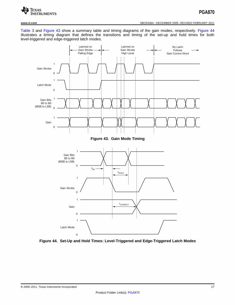
Table 3 and Figure 43 show a summary table and timing diagrams of the gain modes, respectively. Figure 44illustrates a timing diagram that defines the transitions and timing of the set-up and hold times for bothlevel-triggered and edge-triggered latch modes.
Figure 43. Gain Mode Timing
Figure 44. Set-Up and Hold Times: Level-Triggered and Edge-Triggered Latch Modes
© 2009–2011, Texas Instruments Incorporated 17
Product Folder Link(s): PGA870
IN-
OUT-
IN+
OUT+
200 W
+5 V
1k W
B0 to B5
0.1 Fm
75 W
From 50-
Source
W
VMID2
0.1 Fm
VMID1
0.1 Fm
LM(1)
GS(1)
PD
PGA870
0.1 Fm
B0 to B5
PGA870
SBOS436A –DECEMBER 2009–REVISED FEBRUARY 2011 www.ti.com
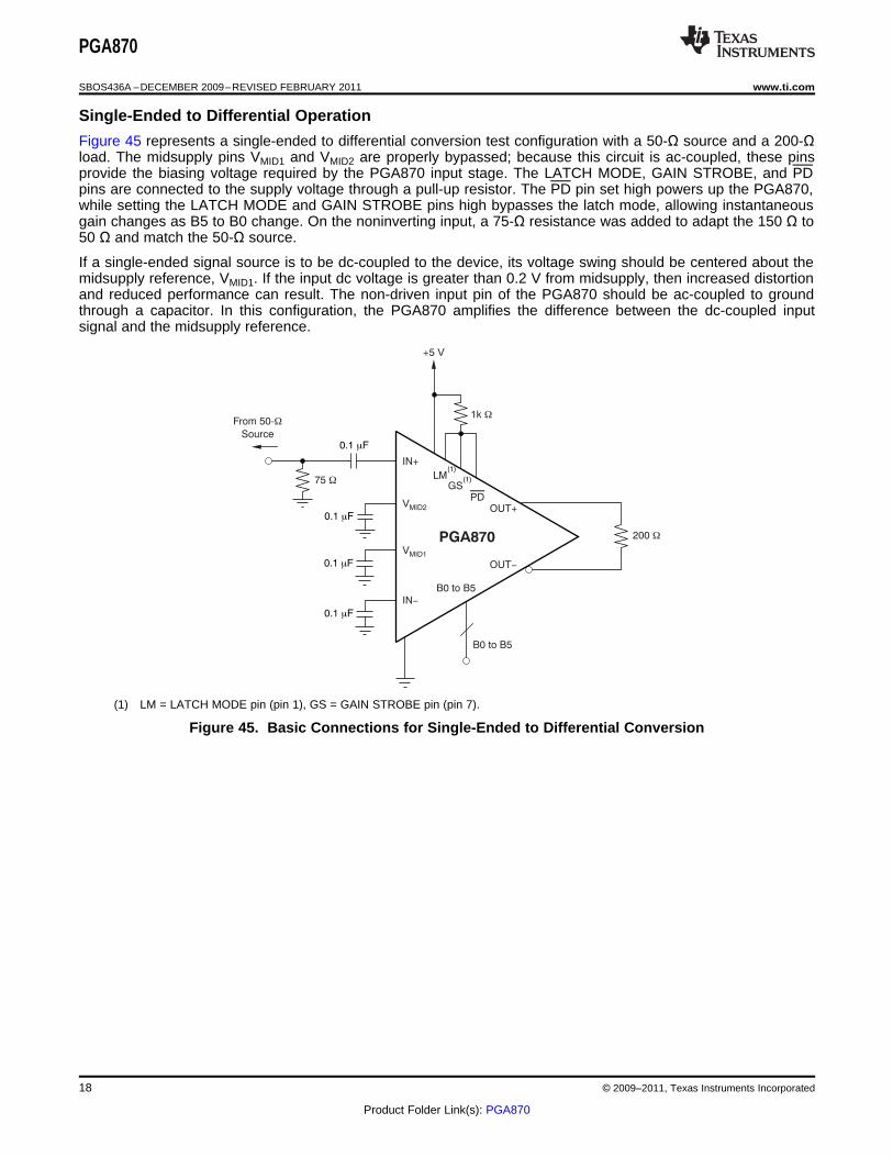
Single-Ended to Differential Operation
Figure 45 represents a single-ended to differential conversion test configuration with a 50-Ω source and a 200-Ωload. The midsupply pins VMID1 and VMID2 are properly bypassed; because this circuit is ac-coupled, these pinsprovide the biasing voltage required by the PGA870 input stage. The LATCH MODE, GAIN STROBE, and PDpins are connected to the supply voltage through a pull-up resistor. The PD pin set high powers up the PGA870,while setting the LATCH MODE and GAIN STROBE pins high bypasses the latch mode, allowing instantaneousgain changes as B5 to B0 change. On the noninverting input, a 75-Ω resistance was added to adapt the 150 Ω to50 Ω and match the 50-Ω source.
If a single-ended signal source is to be dc-coupled to the device, its voltage swing should be centered about themidsupply reference, VMID1. If the input dc voltage is greater than 0.2 V from midsupply, then increased distortionand reduced performance can result. The non-driven input pin of the PGA870 should be ac-coupled to groundthrough a capacitor. In this configuration, the PGA870 amplifies the difference between the dc-coupled inputsignal and the midsupply reference.
(1) LM = LATCH MODE pin (pin 1), GS = GAIN STROBE pin (pin 7).
Figure 45. Basic Connections for Single-Ended to Differential Conversion
18 © 2009–2011, Texas Instruments Incorporated
Product Folder Link(s): PGA870
IN-
OUT-
IN+
OUT+
200 W
+5 V
1k W
B0 to B5
0.1 Fm
0.1 Fm
From 150-
Differential Source
W
VMID2
0.1 Fm
VMID1
0.1 Fm
LM(1)
GS(1)
PD
PGA870
B0 to B5
PGA870
www.ti.com SBOS436A –DECEMBER 2009–REVISED FEBRUARY 2011
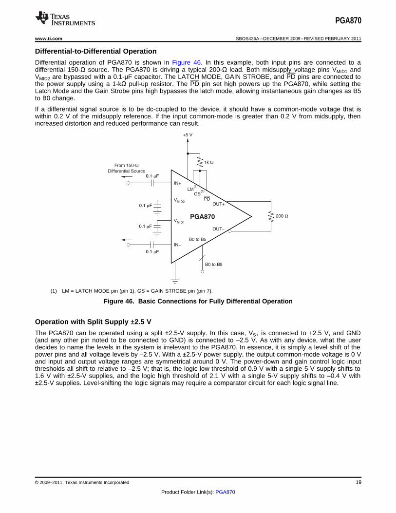
Differential-to-Differential Operation
Differential operation of PGA870 is shown in Figure 46. In this example, both input pins are connected to adifferential 150-Ω source. The PGA870 is driving a typical 200-Ω load. Both midsupply voltage pins VMID1 andVMID2 are bypassed with a 0.1-μF capacitor. The LATCH MODE, GAIN STROBE, and PD pins are connected tothe power supply using a 1-kΩ pull-up resistor. The PD pin set high powers up the PGA870, while setting theLatch Mode and the Gain Strobe pins high bypasses the latch mode, allowing instantaneous gain changes as B5to B0 change.
If a differential signal source is to be dc-coupled to the device, it should have a common-mode voltage that iswithin 0.2 V of the midsupply reference. If the input common-mode is greater than 0.2 V from midsupply, thenincreased distortion and reduced performance can result.
(1) LM = LATCH MODE pin (pin 1), GS = GAIN STROBE pin (pin 7).
Figure 46. Basic Connections for Fully Differential Operation
Operation with Split Supply ±2.5 V
The PGA870 can be operated using a split ±2.5-V supply. In this case, VS+ is connected to +2.5 V, and GND(and any other pin noted to be connected to GND) is connected to –2.5 V. As with any device, what the userdecides to name the levels in the system is irrelevant to the PGA870. In essence, it is simply a level shift of thepower pins and all voltage levels by –2.5 V. With a ±2.5-V power supply, the output common-mode voltage is 0 Vand input and output voltage ranges are symmetrical around 0 V. The power-down and gain control logic inputthresholds all shift to relative to –2.5 V; that is, the logic low threshold of 0.9 V with a single 5-V supply shifts to1.6 V with ±2.5-V supplies, and the logic high threshold of 2.1 V with a single 5-V supply shifts to –0.4 V with±2.5-V supplies. Level-shifting the logic signals may require a comparator circuit for each logic signal line.
© 2009–2011, Texas Instruments Incorporated 19
Product Folder Link(s): PGA870
1/2
TLV3502
+2.5 V
+2.5 V
-2.5 V
Logic to PGA870 Pin
V = +2.5 V, V = 2.5 V-OH OL
2.5-V Input Logic
V = 2.1 V, V = 0.9 VOH OL
R
R
Bandpass
Filter
and
Bias
PGA870
RO
RO
ADC
AIN-
AIN+
CM
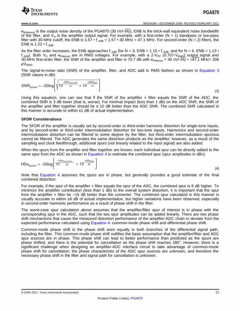
SNR = 10logAmp+Filter = 20logV
eO
Filterout
2
2(
( V
eO
Filterout(
(
with:
e = eFilterout NAmpout ENB
PGA870
SBOS436A –DECEMBER 2009–REVISED FEBRUARY 2011 www.ti.com
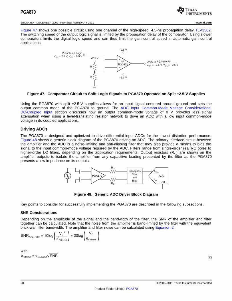
Figure 47 shows one possible circuit using one channel of the high-speed, 4.5-ns propagation delay TLV3502.The switching speed of the output logic signal is limited by the propagation delay of the comparator. Using slowercomparators limits the digital logic speed and can thus limit the gain control speed in automatic gain controlapplications.
Figure 47. Comparator Circuit to Shift Logic Signals to PGA870 Operated on Split ±2.5-V Supplies
Using the PGA870 with split ±2.5-V supplies allows for an input signal centered around ground and sets theoutput common mode of the PGA870 to ground. The ADC Input Common-Mode Voltage Considerations:DC-Coupled Input section discusses how an output common-mode voltage of 0 V provides less signalattenuation when using a level-translating resistor network to drive an ADC with a low input common-modevoltage in dc-coupled applications.
Driving ADCs
The PGA870 is designed and optimized to drive differential input ADCs for the lowest distortion performance.Figure 48 shows a generic block diagram of the PGA870 driving an ADC. The primary interface circuit betweenthe amplifier and the ADC is a noise-limiting and anti-aliasing filter that may also provide a means to bias thesignal to the input common-mode voltage required by the ADC. Filters range from single-order real RC poles tohigher-order LC filters, depending on the application requirements. Output resistors (RO) are shown on theamplifier outputs to isolate the amplifier from any capacitive loading presented by the filter as the PGA870presents a low impedance on its outputs.
Figure 48. Generic ADC Driver Block Diagram
Key points to consider for successfully implementing the PGA870 are described in the following subsections.
SNR Considerations
Depending on the amplitude of the signal and the bandwidth of the filter, the SNR of the amplifier and filtertogether can be calculated. Note that the noise from the amplifier is band-limited by the filter with the equivalentbrick-wall filter bandwidth. The amplifier and filter noise can be calculated using Equation 2.
(2)
20 © 2009–2011, Texas Instruments Incorporated
Product Folder Link(s): PGA870
SNR = 20logSystem -
-SNRAmp+Filter
1010-SNRADC
10+ 10
HDx = 20logSystem -
-HDxAmp+Filter
2010-HDxADC
20+ 10
PGA870
www.ti.com SBOS436A –DECEMBER 2009–REVISED FEBRUARY 2011
eNAmpout is the output noise density of the PGA870 (30 nV/√Hz), ENB is the brick-wall equivalent noise bandwidthof the filter, and VO is the amplifier output signal. For example, with a first-order (N = 1) bandpass or low-passfilter with 30-MHz cutoff, the ENB is 1.57 • f–3dB = 1.57 • 30 MHz = 47.1 MHz. For second-order (N = 2) filters, theENB is 1.22 • f–3dB.
As the filter order increases, the ENB approaches f–3dB (for N = 3, ENB = 1.15 • f–3dB, and for N = 4, ENB = 1.13 •f–3dB). Both VO and eFilterout are in RMS voltages. For example, with a 2-VPP (0.707-VRMS) output signal and30-MHz first-order filter, the SNR of the amplifier and filter is 70.7 dB with eFilterout = 30 nV/√Hz • √47.1 MHz= 206μVRMS.
The signal-to-noise ratio (SNR) of the amplifier, filter, and ADC add in RMS fashion as shown in Equation 3(SNR values in dB):
(3)
Using this equation, one can see that if the SNR of the amplifier + filter equals the SNR of the ADC, thecombined SNR is 3 dB lower (that is, worse). For minimal impact (less than 1 dB) on the ADC SNR, the SNR ofthe amplifier and filter together should be ≥ 10 dB better than the ADC SNR. The combined SNR calculated inthis manner is accurate to within ±1 dB of actual implementation.
SFDR Considerations
The SFDR of the amplifier is usually set by second-order or third-order harmonic distortion for single-tone inputs,and by second-order or third-order intermodulation distortion for two-tone inputs. Harmonics and second-orderintermodulation distortion can be filtered to some degree by the filter, but third-order intermodulation spuriouscannot be filtered. The ADC generates the same distortion products as the amplifier; however, as a result of thesampling and clock feedthrough, additional spurs (not linearly related to the input signal) are also added.
When the spurs from the amplifier and filter together are known, each individual spur can be directly added to thesame spur from the ADC as shown in Equation 4 to estimate the combined spur (spur amplitudes in dBc):
(4)
Note that Equation 4 assumes the spurs are in phase, but generally provides a good estimate of the finalcombined distortion.
For example, if the spur of the amplifier + filter equals the spur of the ADC, the combined spur is 6 dB higher. Tominimize the amplifier contribution (less than 1 dB) to the overall system distortion, it is important that the spurfrom the amplifier + filter be ~15 dB better than the converter. The combined spur calculated in this manner isusually accurate to within ±6 dB of actual implementation, but higher variations have been observed, especiallyin second-order harmonic performance as a result of phase shift in the filter.
The worst-case spur calculation above assumes that the amplifier/filter spur of interest is in phase with thecorresponding spur in the ADC, such that the two spur amplitudes can be added linearly. There are two phaseshift mechanisms that cause the measured distortion performance of the amplifier-ADC chain to deviate from theexpected performance calculated using Equation 4: common-mode phase shift and differential phase shift.
Common-mode phase shift is the phase shift seen equally in both branches of the differential signal path,including the filter. This common-mode phase shift nullifies the basic assumption that the amplifier/filter and ADCspur sources are in phase. This phase shift can lead to better performance than predicted as the spurs arephase shifted, and there is the potential for cancellation as the phase shift reaches 180°. However, there is asignificant challenge when designing an amplifier-ADC interface circuit to take advantage of common-modephase shift for cancellation: the phase characteristic of the ADC spur sources are unknown, and therefore thenecessary phase shift in the filter and signal path for cancellation is unknown.
© 2009–2011, Texas Instruments Incorporated 21
Product Folder Link(s): PGA870
PGA870
RO
RCM
RCM
RO
ADC
AIN-
AIN+
CM
PGA870
SBOS436A –DECEMBER 2009–REVISED FEBRUARY 2011 www.ti.com
Differential phase shift is the difference in the phase response between the two branches of the differential filtersignal path. Differential phase shift in the filter as a result of mismatched components caused by nominaltolerance can severely degrade the even-order distortion of the amplifier-ADC chain. This condition has the sameeffect as mismatched path lengths for the two differential traces, and causes more phase shift in one path thanthe other. Ideally, the phase response over frequency through the two sides of a differential signal path areidentical, such that even-order harmonics remain optimally out of phase and cancel when the signal is takendifferentially. However, if one side has more phase shift than the other, then the even-order harmoniccancellation is not as effective.
Single-order RC filters cause very little differential phase shift with nominal tolerances of 5% or less, buthigher-order LC filters are very sensitive to component mismatch. For instance, a third-order Butterworthbandpass filter with 100-MHz center frequency and 20-MHz bandwidth shows up to 20° differential phaseimbalance in a Spice Monte Carlo analysis with 2% component tolerances. Therefore, while a prototype maywork, production variance is unacceptable. In ac-coupled applications that require second- and higher-orderfilters between the PGA870 and ADC, a transformer or balun is recommended at the ADC input to restore thephase balance. For dc-coupled applications where a transformer or balun at the ADC input cannot be used, it isrecommended to use first- or second-order filters to minimize the effects of differential phase shift as a result ofcomponent tolerance.
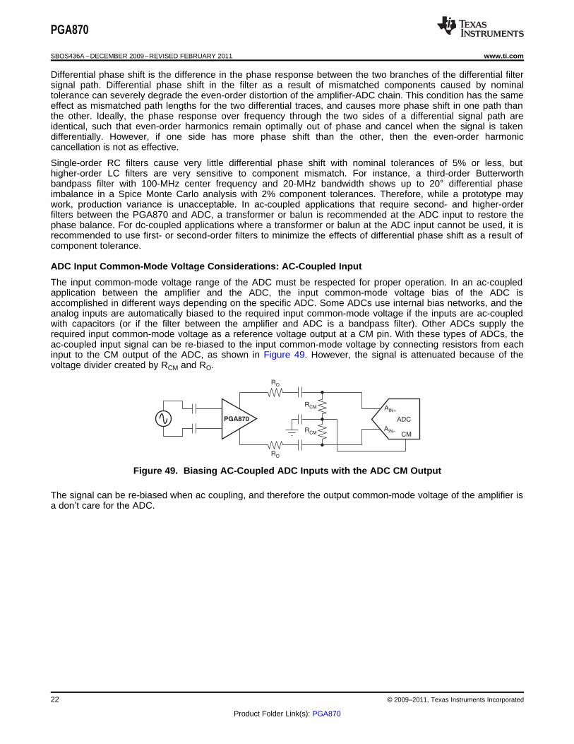
ADC Input Common-Mode Voltage Considerations: AC-Coupled Input
The input common-mode voltage range of the ADC must be respected for proper operation. In an ac-coupledapplication between the amplifier and the ADC, the input common-mode voltage bias of the ADC isaccomplished in different ways depending on the specific ADC. Some ADCs use internal bias networks, and theanalog inputs are automatically biased to the required input common-mode voltage if the inputs are ac-coupledwith capacitors (or if the filter between the amplifier and ADC is a bandpass filter). Other ADCs supply therequired input common-mode voltage as a reference voltage output at a CM pin. With these types of ADCs, theac-coupled input signal can be re-biased to the input common-mode voltage by connecting resistors from eachinput to the CM output of the ADC, as shown in Figure 49. However, the signal is attenuated because of thevoltage divider created by RCM and RO.
Figure 49. Biasing AC-Coupled ADC Inputs with the ADC CM Output
The signal can be re-biased when ac coupling, and therefore the output common-mode voltage of the amplifier isa don’t care for the ADC.
22 © 2009–2011, Texas Instruments Incorporated
Product Folder Link(s): PGA870
Amp
RO
RO
ADC
CIN
VAMP-
VAMP+
VADC-
VADC+
VREF
RP
RIN
RP
VREF
R = RP O
V V
V V
ADC REF
AMP CM
-
-
GAIN =2R || ZP IN
2R + 2R || ZO P IN
R = 2R + 2R || ZL O P IN
V =AMP_PP
V
GAINADC_FS
PGA870
www.ti.com SBOS436A –DECEMBER 2009–REVISED FEBRUARY 2011
ADC Input Common-Mode Voltage Considerations: DC-Coupled Input
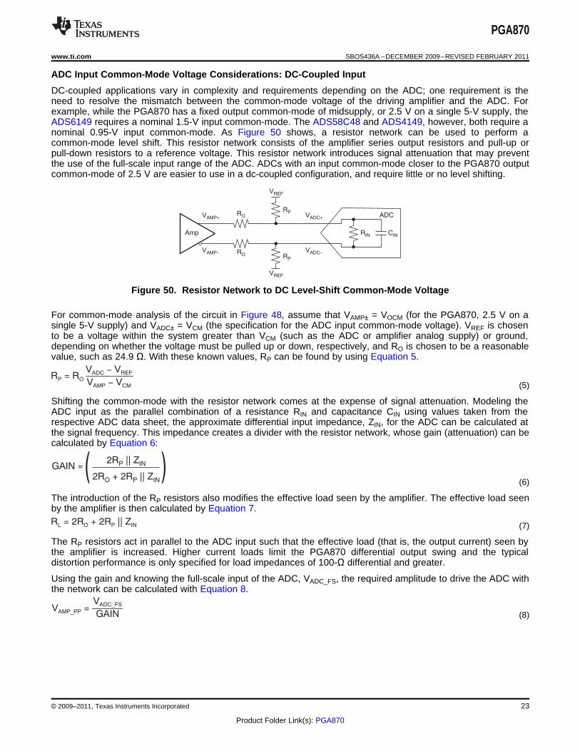
DC-coupled applications vary in complexity and requirements depending on the ADC; one requirement is theneed to resolve the mismatch between the common-mode voltage of the driving amplifier and the ADC. Forexample, while the PGA870 has a fixed output common-mode of midsupply, or 2.5 V on a single 5-V supply, theADS6149 requires a nominal 1.5-V input common-mode. The ADS58C48 and ADS4149, however, both require anominal 0.95-V input common-mode. As Figure 50 shows, a resistor network can be used to perform acommon-mode level shift. This resistor network consists of the amplifier series output resistors and pull-up orpull-down resistors to a reference voltage. This resistor network introduces signal attenuation that may preventthe use of the full-scale input range of the ADC. ADCs with an input common-mode closer to the PGA870 outputcommon-mode of 2.5 V are easier to use in a dc-coupled configuration, and require little or no level shifting.
Figure 50. Resistor Network to DC Level-Shift Common-Mode Voltage
For common-mode analysis of the circuit in Figure 48, assume that VAMP± = VOCM (for the PGA870, 2.5 V on asingle 5-V supply) and VADC± = VCM (the specification for the ADC input common-mode voltage). VREF is chosento be a voltage within the system greater than VCM (such as the ADC or amplifier analog supply) or ground,depending on whether the voltage must be pulled up or down, respectively, and RO is chosen to be a reasonablevalue, such as 24.9 Ω. With these known values, RP can be found by using Equation 5.
(5)
Shifting the common-mode with the resistor network comes at the expense of signal attenuation. Modeling theADC input as the parallel combination of a resistance RIN and capacitance CIN using values taken from therespective ADC data sheet, the approximate differential input impedance, ZIN, for the ADC can be calculated atthe signal frequency. This impedance creates a divider with the resistor network, whose gain (attenuation) can becalculated by Equation 6:
(6)
The introduction of the RP resistors also modifies the effective load seen by the amplifier. The effective load seenby the amplifier is then calculated by Equation 7.
(7)
The RP resistors act in parallel to the ADC input such that the effective load (that is, the output current) seen bythe amplifier is increased. Higher current loads limit the PGA870 differential output swing and the typicaldistortion performance is only specified for load impedances of 100-Ω differential and greater.
Using the gain and knowing the full-scale input of the ADC, VADC_FS, the required amplitude to drive the ADC withthe network can be calculated with Equation 8.
(8)
© 2009–2011, Texas Instruments Incorporated 23
Product Folder Link(s): PGA870
PGA870
SBOS436A –DECEMBER 2009–REVISED FEBRUARY 2011 www.ti.com
Using the ADC examples given previously, Table 4 shows sample calculations of the value of RP and VAMP_FS forfull-scale drive, and then for –1 dBFS.
Table 4. Example RP for Various ADCs
ADCRIN || CIN VAMP_PP
at for 0 VAMP_PPVAMP VCM VREF 170 MHz RO RP GAIN GAIN VADC_FS dBFS –1 dBFS
ADC (VDC) (VDC) (VDC) (Ω) (Ω) (Ω) (V/V) (dB) (VPP) (VPP) (VPP)
ADS6149 2.5 1.5 0 216 25 37.5 0.53 –5.57 2 3.80 3.38
ADS58C48/ 2.5 0.95 0 195 25 15.3 0.35 –9.21 2 5.78 5.15ADS4149
ADS58C48/ 0 0.95 2.5 195 25 40.8 0.53 –5.43 2 3.74 3.33ADS4149 (1)
(1) PGA870 operated with ±2.5-V supply.
As Table 4 shows, the signal attenuation as a result of the added resistor network increases as the requiredcommon-mode shift increases. For the ADS6149, the required common-mode level shift is –1 V, from 2.5 V to1.5 V, and the signal attenuates by 5.57 dB. This difference is a significant signal loss, and the amplifier outputmust be increased (either by increasing the PGA870 input or the PGA870 gain) to make up for the loss in orderto drive the full-scale input of the ADC for the highest SNR. At the same time, increasing the amplifier outputswing results in degraded distortion performance as the amplifier output approaches its output range limits.
For the ADS58C48/ADS4149 case with the PGA870 operated with a single 5-V supply, the required level shiftis –1.55 V and the signal attenuates by 9.21 dB. This signal loss cannot be fully recovered by increasing thePGA870 output: the differential output swing required at the PGA870 output to drive the full-scale range of theADS58C48/ADS4149 exceeds the PGA870 output swing capability. Additionally, the distortion performance ofthe amplifier is degraded as the output swing increases. In these configurations, the maximum recommendedADC input is –6 dBFS in order to limit the impact of the additional loading. Another option is to operate thePGA870 with a split ±2.5-V supply, with the resulting calculations shown in the last row of Table 4. For thissituation, if +2.5 V is used as the VREF pull-up voltage, the PGA870 only needs to drive 3.33 VPP at its output todrive the ADS58C48/ADS4149 input to –1 dBFS. See the Operation with Split Supply ±2.5V section for moredetails on using the PGA870 with split supplies.
As with any design, testing is recommended to validate whether the result meets the specific design goals.
PGA870 Driving ADS58C48
To illustrate the performance of the PGA870 as an ADC driver, the PGA870 is tested with the ADS58C48 andbandpass filter designs centered at an operating frequency of 170 MHz. The ADS58C48 is a quad-channel,11-bit, 200-MSPS ADC with LVDS-compatible digital outputs on six data pairs per channel. The device hasunbuffered analog inputs. There are several key information points to consider when interfacing to the PGA870:• Unbuffered analog inputs with a frequency-dependent input impedance of ZIN = RIN || CIN
• 0.95-V analog input common-mode voltage• SNR = 66.1 dBFS (typ) at fIN = 17 0MHz• SFDR = 80 dBc (typ) at fIN = 170 MHz• HD2 = 82 dBc (typ) at fIN = 170 MHz• HD3 = 80 dBc (typ) at fIN = 170 MHz• IMD = 83 dBFS (typ) with two-tone input fIN1 = 185 MHz, fIN2 = 190 MHz
The ADS58C48EVM is designed for flexible options to ease design work. Used in conjunction with theTSW1200EVM High-Speed ADC LVDS Evaluation System, it reduces evaluation time to help the designer movefrom prototype to production more quickly.
The ADS58C48EVM provides back-to-back input transformers for each of the four analog input channels in orderto convert single-ended test signals to differential when driving the ADCs directly. The Channel D path on theEVM, however, provides an alternate path (selectable via jumper resistors) for driving the channel with anonboard PGA870. In this path, a single-ended input test signal can be converted to differential with a singletransformer to drive the PGA870 input. The EVM provides various component pads between the PGA870 andADS58C48 input for implementing various filter types. For the latest schematic of the EVM, refer to theADS58C48EVM Design Package available through the ADS58C48EVM product page on the TI website.
24 © 2009–2011, Texas Instruments Incorporated
Product Folder Link(s): PGA870
R10
15 W
R2
25 W
C2
100 nF
R9
15 W
R1
100 W
R11
100 W
L13
8.2 nH
R3
25 W
C3
100 nF
C18
68 pF
C17
100 nF
ADC+
ADC-
ADC VCM
PGA870
www.ti.com SBOS436A –DECEMBER 2009–REVISED FEBRUARY 2011
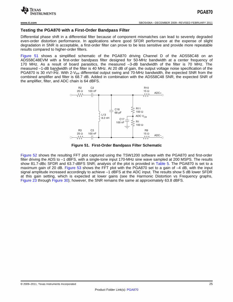
Testing the PGA870 with a First-Order Bandpass Filter
Differential phase shift in a differential filter because of component mismatches can lead to severely degradedeven-order distortion performance. In applications where good SFDR performance at the expense of slightdegradation in SNR is acceptable, a first-order filter can prove to be less sensitive and provide more repeatableresults compared to higher-order filters.
Figure 51 shows a simplified schematic of the PGA870 driving Channel D of the ADS58C48 on anADS58C48EVM with a first-order bandpass filter designed for 50-MHz bandwidth at a center frequency of170 MHz. As a result of board parasitics, the measured –3-dB bandwidth of the filter is 70 MHz. Themeasured –1-dB bandwidth of the filter is 40 MHz. At 20 dB of gain, the output voltage noise specification of thePGA870 is 30 nV/√Hz. With 2-VPP differential output swing and 70-MHz bandwidth, the expected SNR from thecombined amplifier and filter is 68.7 dB. Added in combination with the ADS58C48 SNR, the expected SNR ofthe amplifier, filter, and ADC chain is 64 dBFS.
Figure 51. First-Order Bandpass Filter Schematic
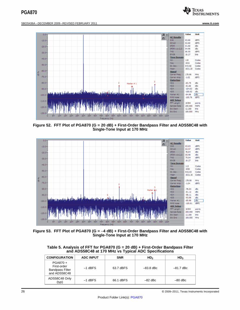
Figure 52 shows the resulting FFT plot captured using the TSW1200 software with the PGA870 and first-orderfilter driving the ADS to –1 dBFS, with a single-tone input 170-MHz sine wave sampled at 200 MSPS. The resultsshow 81.7-dBc SFDR and 63.7-dBFS SNR; analysis of the plot is provided in Table 5. The PGA870 is set to amaximum gain of 20 dB. Figure 53 shows the FFT plot with the PGA870 set to a gain of –4 dB, with the inputsignal amplitude increased accordingly to achieve –1 dBFS at the ADC input. The results show 5 dB lower SFDRat this gain setting, which is expected at lower gains (see the Harmonic Distortion vs Frequency graphs,Figure 23 through Figure 30); however, the SNR remains the same at approximately 63.8 dBFS.
© 2009–2011, Texas Instruments Incorporated 25
Product Folder Link(s): PGA870
PGA870
SBOS436A –DECEMBER 2009–REVISED FEBRUARY 2011 www.ti.com
Figure 52. FFT Plot of PGA870 (G = 20 dB) + First-Order Bandpass Filter and ADS58C48 withSingle-Tone Input at 170 MHz
Figure 53. FFT Plot of PGA870 (G = –4 dB) + First-Order Bandpass Filter and ADS58C48 withSingle-Tone Input at 170 MHz
Table 5. Analysis of FFT for PGA870 (G = 20 dB) + First-Order Bandpass Filterand ADS58C48 at 170 MHz vs Typical ADC Specifications
CONFIGURATION ADC INPUT SNR HD2 HD3
PGA870 +First-order –1 dBFS 63.7 dBFS –83.8 dBc –81.7 dBcBandpass Filter
and ADS58C48
ADS58C48 Only –1 dBFS 66.1 dBFS –82 dBc –80 dBc(typ)
26 © 2009–2011, Texas Instruments Incorporated
Product Folder Link(s): PGA870
PGA870
www.ti.com SBOS436A –DECEMBER 2009–REVISED FEBRUARY 2011
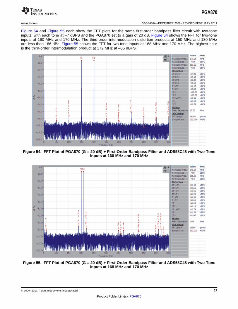
Figure 54 and Figure 55 each show the FFT plots for the same first-order bandpass filter circuit with two-toneinputs, with each tone at –7 dBFS and the PGA870 set to a gain of 20 dB. Figure 54 shows the FFT for two-toneinputs at 160 MHz and 170 MHz. The third-order intermodulation distortion products at 150 MHz and 180 MHzare less than –86 dBc. Figure 55 shows the FFT for two-tone inputs at 168 MHz and 170 MHz. The highest spuris the third-order intermodulation product at 172 MHz at –85 dBFS.
Figure 54. FFT Plot of PGA870 (G = 20 dB) + First-Order Bandpass Filter and ADS58C48 with Two-ToneInputs at 160 MHz and 170 MHz
Figure 55. FFT Plot of PGA870 (G = 20 dB) + First-Order Bandpass Filter and ADS58C48 with Two-ToneInputs at 168 MHz and 170 MHz
© 2009–2011, Texas Instruments Incorporated 27
Product Folder Link(s): PGA870
R10
15 W
L16
56 nH
L17
56 nH
R2
25 W
C21
15 nF
R9
15 W
R1
100 W
R11
100 W
R13
49.9 W
R12
49.9 W
L15
8.2 nH
R3
25 W
C22
15 nF
C23
100 pFC20
3.3 pFC17
100 nF
ADC+
ADC-
ADC VCM
PGA870
SBOS436A –DECEMBER 2009–REVISED FEBRUARY 2011 www.ti.com
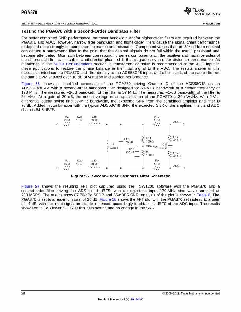
Testing the PGA870 with a Second-Order Bandpass Filter
For better combined SNR performance, narrower bandwidth and/or higher-order filters are required between thePGA870 and ADC. However, narrow filter bandwidth and highe-order filters cause the signal chain performanceto depend more strongly on component tolerance and mismatch. Component values that are 5% off from nominalcan detune a narrowband filter to the point that the desired signals do not fall within the useful passband andbecome attenuated. Mismatch between corresponding series components on the positive and negative sides ofthe differential filter can result in a differential phase shift that degrades even-order distortion performance. Asmentioned in the SFDR Considerations section, a transformer or balun is recommended at the ADC input inthese applications to restore the phase balance in the input signal to the ADC. The results shown in thisdiscussion interface the PGA870 and filter directly to the ADS58C48 input, and other builds of the same filter onthe same EVM showed over 10 dB of variation in distortion performance.
Figure 56 shows a simplified schematic of the PGA870 driving Channel D of the ADS58C48 on anADS58C48EVM with a second-order bandpass filter designed for 50-MHz bandwidth at a center frequency of170 MHz. The measured –3-dB bandwidth of the filter is 57 MHz. The measured –1-dB bandwidth of the filter is34 MHz. At a gain of 20 dB, the output voltage noise specification of the PGA870 is 30 nV/√Hz. With 2-VPPdifferential output swing and 57-MHz bandwidth, the expected SNR from the combined amplifier and filter is70 dB. Added in combination with the typical ADS58C48 SNR, the expected SNR of the amplifier, filter, and ADCchain is 64.5 dBFS.
Figure 56. Second-Order Bandpass Filter Schematic
Figure 57 shows the resulting FFT plot captured using the TSW1200 software with the PGA870 and asecond-order filter driving the ADS to –1 dBFS, with a single-tone input 170-MHz sine wave sampled at200 MSPS. The results show 87.76-dBc SFDR and 65-dBFS SNR; analysis of the plot is shown in Table 6. ThePGA870 is set to a maximum gain of 20 dB. Figure 58 shows the FFT plot with the PGA870 set instead to a gainof –4 dB, with the input signal amplitude increased accordingly to obtain –1 dBFS at the ADC input. The resultsshow about 1 dB lower SFDR at this gain setting and no change in the SNR.
28 © 2009–2011, Texas Instruments Incorporated
Product Folder Link(s): PGA870
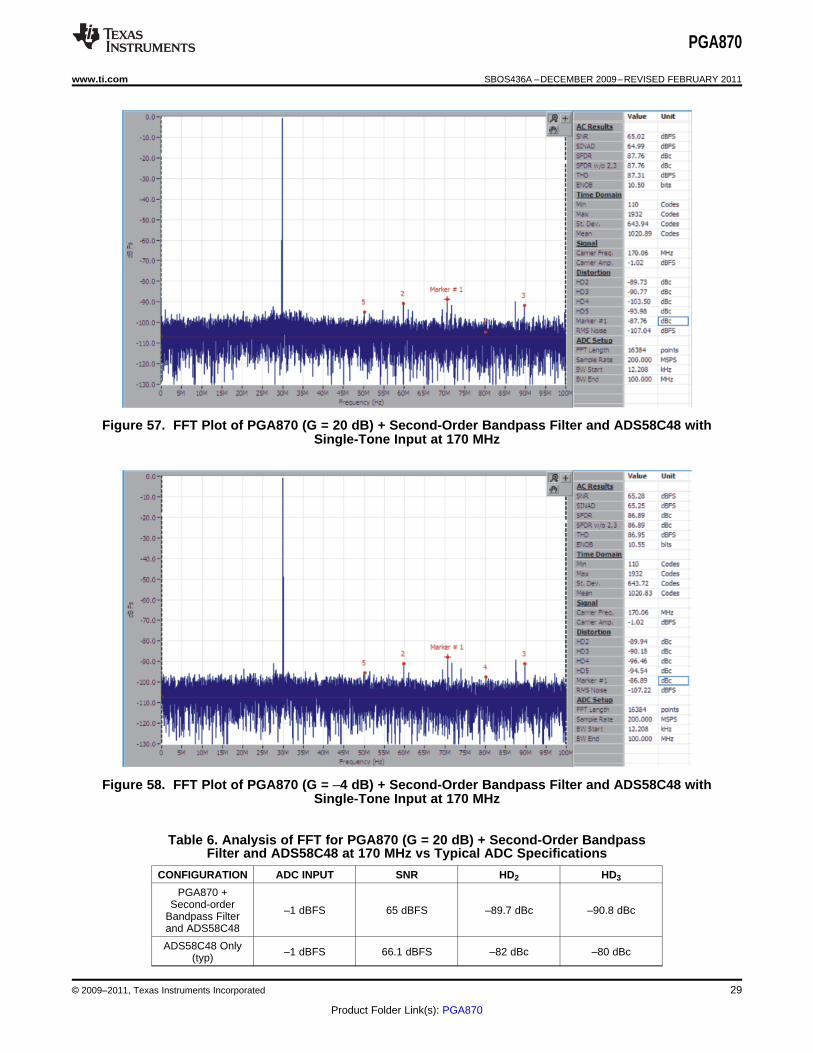
PGA870
www.ti.com SBOS436A –DECEMBER 2009–REVISED FEBRUARY 2011
Figure 57. FFT Plot of PGA870 (G = 20 dB) + Second-Order Bandpass Filter and ADS58C48 withSingle-Tone Input at 170 MHz
Figure 58. FFT Plot of PGA870 (G = –4 dB) + Second-Order Bandpass Filter and ADS58C48 withSingle-Tone Input at 170 MHz
Table 6. Analysis of FFT for PGA870 (G = 20 dB) + Second-Order BandpassFilter and ADS58C48 at 170 MHz vs Typical ADC Specifications
CONFIGURATION ADC INPUT SNR HD2 HD3
PGA870 +Second-order –1 dBFS 65 dBFS –89.7 dBc –90.8 dBcBandpass Filter
and ADS58C48
ADS58C48 Only –1 dBFS 66.1 dBFS –82 dBc –80 dBc(typ)
© 2009–2011, Texas Instruments Incorporated 29
Product Folder Link(s): PGA870
PGA870
SBOS436A –DECEMBER 2009–REVISED FEBRUARY 2011 www.ti.com
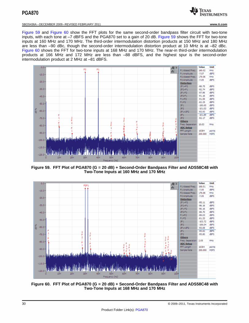
Figure 59 and Figure 60 show the FFT plots for the same second-order bandpass filter circuit with two-toneinputs, with each tone at –7 dBFS and the PGA870 set to a gain of 20 dB. Figure 59 shows the FFT for two-toneinputs at 160 MHz and 170 MHz. The third-order intermodulation distortion products at 150 MHz and 180 MHzare less than –90 dBc, though the second-order intermodulation distortion product at 10 MHz is at –82 dBc.Figure 60 shows the FFT for two-tone inputs at 168 MHz and 170 MHz. The near-in third-order intermodulationproducts at 166 MHz and 172 MHz are less than –88 dBFS, and the highest spur is the second-orderintermodulation product at 2 MHz at –81 dBFS.
Figure 59. FFT Plot of PGA870 (G = 20 dB) + Second-Order Bandpass Filter and ADS58C48 withTwo-Tone Inputs at 160 MHz and 170 MHz
Figure 60. FFT Plot of PGA870 (G = 20 dB) + Second-Order Bandpass Filter and ADS58C48 withTwo-Tone Inputs at 168 MHz and 170 MHz
30 © 2009–2011, Texas Instruments Incorporated
Product Folder Link(s): PGA870
PGA870
www.ti.com SBOS436A –DECEMBER 2009–REVISED FEBRUARY 2011
PCB Layout Recommendations
Complete information about the PGA870EVM is found in the PGA870EVM User Guide, available for downloadthrough the PGA870 product folder on the TI web site. Printed circuit board (PCB) layout should follow thesegeneral guidelines:1. Signal routing should be direct and as short as possible into and out of the device input and output pins.
Routing the signal path between layers using vias should be avoided if possible.2. The device PowerPAD should be connected to a solid ground plane with multiple vias. The PowerPAD must
be connected to electrical ground. Consult the PGA870EVM User Guide for a layout example.3. Ground or power planes should be removed from directly under the amplifier output pins.4. A 0.1-μF capacitor should be placed between the VMIDpin and ground near to the pin.5. An output resistor is recommended in each output lead, placed as near to the output pins as possible.6. Two 0.1-μF power-supply decoupling capacitors should be placed as near to the power-supply pins as
possible.7. Two 10-μF power-supply decoupling capacitors should be placed within 1 in (2,54 cm) of the device.8. The digital control pins use CMOS logic levels for high and low signals, but can tolerate being pulled high to
a +5-V power supply. The digital control pins do not have internal pull-up resistors.
© 2009–2011, Texas Instruments Incorporated 31
Product Folder Link(s): PGA870
PGA870
SBOS436A –DECEMBER 2009–REVISED FEBRUARY 2011 www.ti.com
REVISION HISTORY
NOTE: Page numbers for previous revisions may differ from page numbers in the current version.
Changes from Original (December, 2009) to Revision A Page
• Updated Related Products table ........................................................................................................................................... 1
• Changed storage temperature range specification in Absolute Maximum Ratings table ..................................................... 2
• Moved noise figure parameter to AC Performance section of Electrical Characteristics (VS = +5 V) table ......................... 3
• Added output-referred voltage noise parameter to Electrical Characteristics (VS = +5 V) table .......................................... 3
• Added Figure 31 ................................................................................................................................................................. 12
• Revised second paragraph of Single-Ended to Differential Operation section .................................................................. 18
• Added new paragraph to Differential-to-Differential Operation section .............................................................................. 19
• Added Operation with Split Supply ±2.5V section .............................................................................................................. 19
• Added Driving ADCs section .............................................................................................................................................. 20
• Added PGA870 Driving ADS58C48 section ....................................................................................................................... 24
• Added Testing the PGA870 with a First-Order Bandpass Filter section ............................................................................ 25
• Added Testing the PGA870 with a Second-Order Bandpass Filter section ....................................................................... 28
32 © 2009–2011, Texas Instruments Incorporated
Product Folder Link(s): PGA870
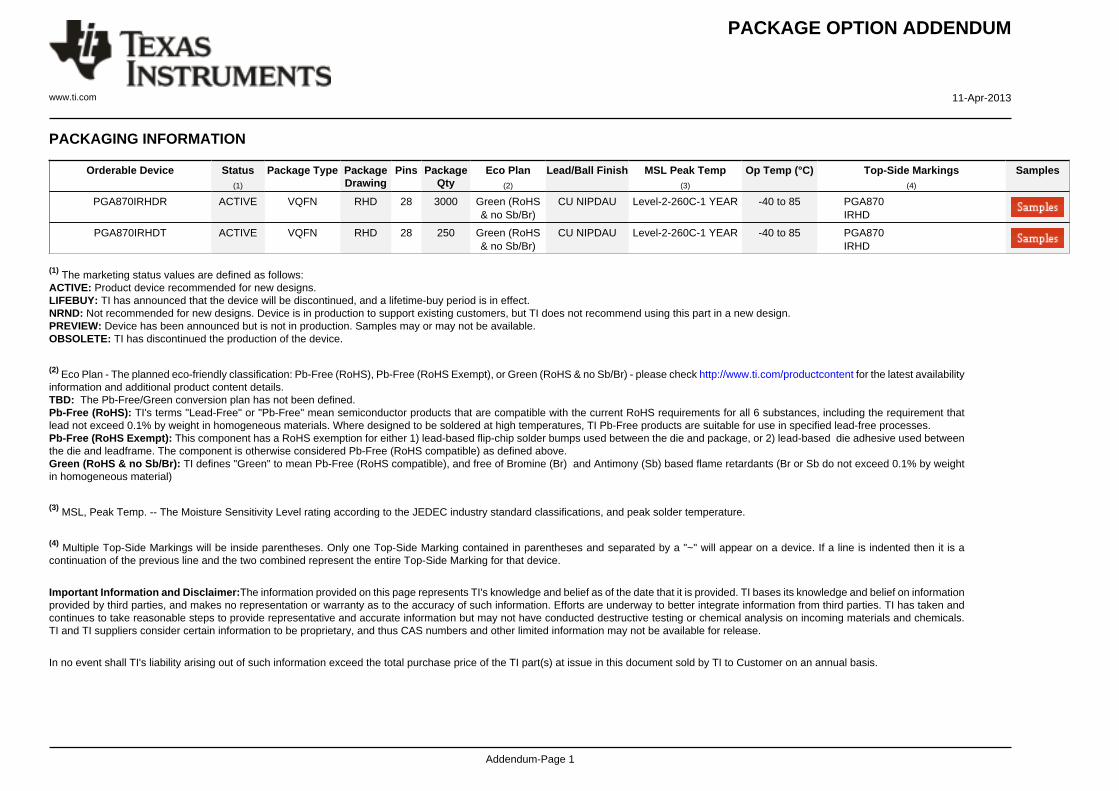
PACKAGE OPTION ADDENDUM
www.ti.com 11-Apr-2013
Addendum-Page 1
PACKAGING INFORMATION
Orderable Device Status(1)
Package Type PackageDrawing
Pins PackageQty
Eco Plan(2)
Lead/Ball Finish MSL Peak Temp(3)
Op Temp (°C) Top-Side Markings(4)
Samples
PGA870IRHDR ACTIVE VQFN RHD 28 3000 Green (RoHS& no Sb/Br)
CU NIPDAU Level-2-260C-1 YEAR -40 to 85 PGA870IRHD
PGA870IRHDT ACTIVE VQFN RHD 28 250 Green (RoHS& no Sb/Br)
CU NIPDAU Level-2-260C-1 YEAR -40 to 85 PGA870IRHD
(1) The marketing status values are defined as follows:ACTIVE: Product device recommended for new designs.LIFEBUY: TI has announced that the device will be discontinued, and a lifetime-buy period is in effect.NRND: Not recommended for new designs. Device is in production to support existing customers, but TI does not recommend using this part in a new design.PREVIEW: Device has been announced but is not in production. Samples may or may not be available.OBSOLETE: TI has discontinued the production of the device.
(2) Eco Plan - The planned eco-friendly classification: Pb-Free (RoHS), Pb-Free (RoHS Exempt), or Green (RoHS & no Sb/Br) - please check http://www.ti.com/productcontent for the latest availabilityinformation and additional product content details.TBD: The Pb-Free/Green conversion plan has not been defined.Pb-Free (RoHS): TI's terms "Lead-Free" or "Pb-Free" mean semiconductor products that are compatible with the current RoHS requirements for all 6 substances, including the requirement thatlead not exceed 0.1% by weight in homogeneous materials. Where designed to be soldered at high temperatures, TI Pb-Free products are suitable for use in specified lead-free processes.Pb-Free (RoHS Exempt): This component has a RoHS exemption for either 1) lead-based flip-chip solder bumps used between the die and package, or 2) lead-based die adhesive used betweenthe die and leadframe. The component is otherwise considered Pb-Free (RoHS compatible) as defined above.Green (RoHS & no Sb/Br): TI defines "Green" to mean Pb-Free (RoHS compatible), and free of Bromine (Br) and Antimony (Sb) based flame retardants (Br or Sb do not exceed 0.1% by weightin homogeneous material)
(3) MSL, Peak Temp. -- The Moisture Sensitivity Level rating according to the JEDEC industry standard classifications, and peak solder temperature.
(4) Multiple Top-Side Markings will be inside parentheses. Only one Top-Side Marking contained in parentheses and separated by a "~" will appear on a device. If a line is indented then it is acontinuation of the previous line and the two combined represent the entire Top-Side Marking for that device.
Important Information and Disclaimer:The information provided on this page represents TI's knowledge and belief as of the date that it is provided. TI bases its knowledge and belief on informationprovided by third parties, and makes no representation or warranty as to the accuracy of such information. Efforts are underway to better integrate information from third parties. TI has taken andcontinues to take reasonable steps to provide representative and accurate information but may not have conducted destructive testing or chemical analysis on incoming materials and chemicals.TI and TI suppliers consider certain information to be proprietary, and thus CAS numbers and other limited information may not be available for release.
In no event shall TI's liability arising out of such information exceed the total purchase price of the TI part(s) at issue in this document sold by TI to Customer on an annual basis.
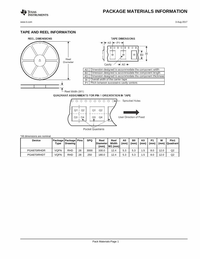
TAPE AND REEL INFORMATION
*All dimensions are nominal
Device PackageType
PackageDrawing
Pins SPQ ReelDiameter
(mm)
ReelWidth
W1 (mm)
A0(mm)
B0(mm)
K0(mm)
P1(mm)
W(mm)
Pin1Quadrant
PGA870IRHDR VQFN RHD 28 3000 330.0 12.4 5.3 5.3 1.5 8.0 12.0 Q2
PGA870IRHDT VQFN RHD 28 250 180.0 12.4 5.3 5.3 1.5 8.0 12.0 Q2
PACKAGE MATERIALS INFORMATION
www.ti.com 3-Aug-2017
Pack Materials-Page 1
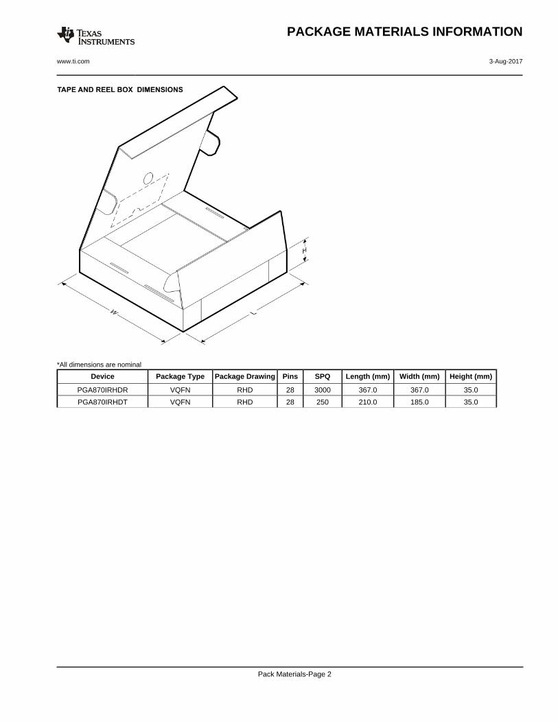
*All dimensions are nominal
Device Package Type Package Drawing Pins SPQ Length (mm) Width (mm) Height (mm)
PGA870IRHDR VQFN RHD 28 3000 367.0 367.0 35.0
PGA870IRHDT VQFN RHD 28 250 210.0 185.0 35.0
PACKAGE MATERIALS INFORMATION
www.ti.com 3-Aug-2017
Pack Materials-Page 2
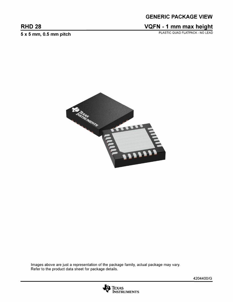
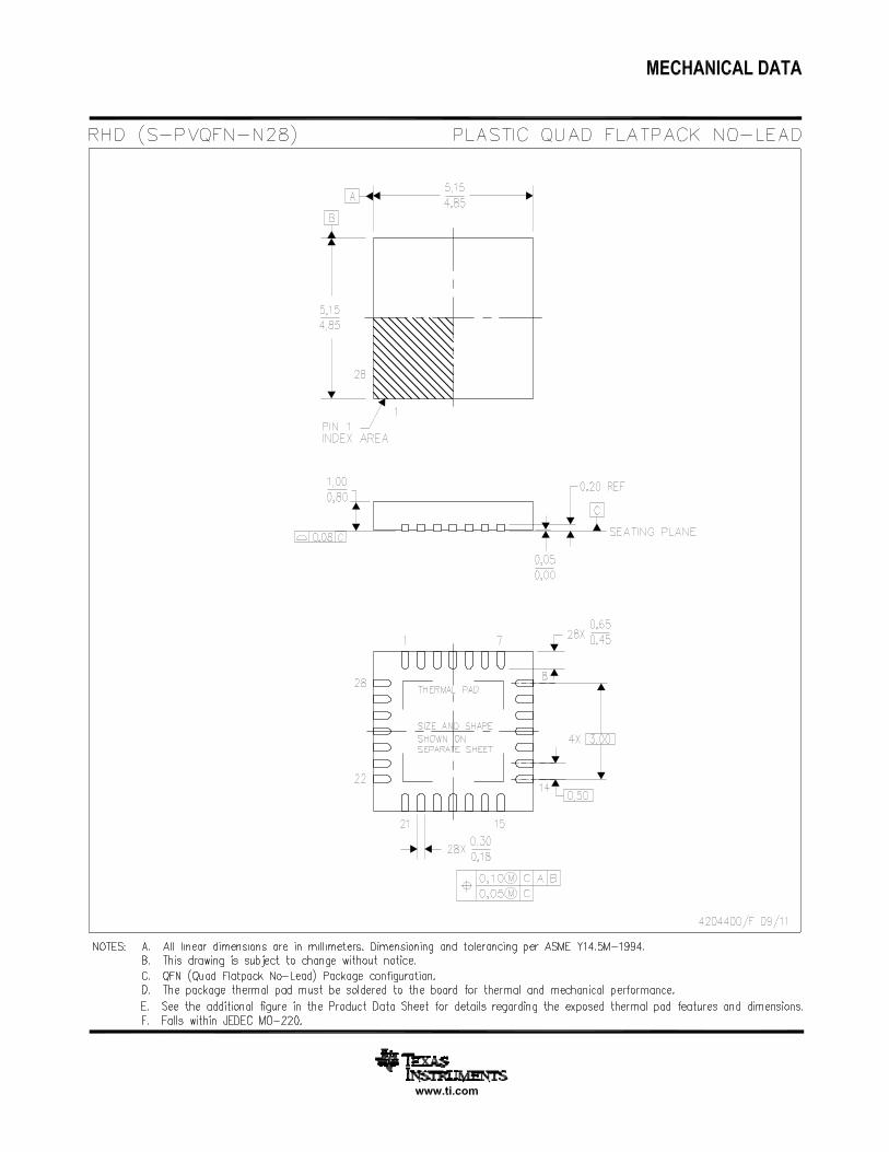

IMPORTANT NOTICE
Texas Instruments Incorporated (TI) reserves the right to make corrections, enhancements, improvements and other changes to itssemiconductor products and services per JESD46, latest issue, and to discontinue any product or service per JESD48, latest issue. Buyersshould obtain the latest relevant information before placing orders and should verify that such information is current and complete.TI’s published terms of sale for semiconductor products (http://www.ti.com/sc/docs/stdterms.htm) apply to the sale of packaged integratedcircuit products that TI has qualified and released to market. Additional terms may apply to the use or sale of other types of TI products andservices.Reproduction of significant portions of TI information in TI data sheets is permissible only if reproduction is without alteration and isaccompanied by all associated warranties, conditions, limitations, and notices. TI is not responsible or liable for such reproduceddocumentation. Information of third parties may be subject to additional restrictions. Resale of TI products or services with statementsdifferent from or beyond the parameters stated by TI for that product or service voids all express and any implied warranties for theassociated TI product or service and is an unfair and deceptive business practice. TI is not responsible or liable for any such statements.Buyers and others who are developing systems that incorporate TI products (collectively, “Designers”) understand and agree that Designersremain responsible for using their independent analysis, evaluation and judgment in designing their applications and that Designers havefull and exclusive responsibility to assure the safety of Designers' applications and compliance of their applications (and of all TI productsused in or for Designers’ applications) with all applicable regulations, laws and other applicable requirements. Designer represents that, withrespect to their applications, Designer has all the necessary expertise to create and implement safeguards that (1) anticipate dangerousconsequences of failures, (2) monitor failures and their consequences, and (3) lessen the likelihood of failures that might cause harm andtake appropriate actions. Designer agrees that prior to using or distributing any applications that include TI products, Designer willthoroughly test such applications and the functionality of such TI products as used in such applications.TI’s provision of technical, application or other design advice, quality characterization, reliability data or other services or information,including, but not limited to, reference designs and materials relating to evaluation modules, (collectively, “TI Resources”) are intended toassist designers who are developing applications that incorporate TI products; by downloading, accessing or using TI Resources in anyway, Designer (individually or, if Designer is acting on behalf of a company, Designer’s company) agrees to use any particular TI Resourcesolely for this purpose and subject to the terms of this Notice.TI’s provision of TI Resources does not expand or otherwise alter TI’s applicable published warranties or warranty disclaimers for TIproducts, and no additional obligations or liabilities arise from TI providing such TI Resources. TI reserves the right to make corrections,enhancements, improvements and other changes to its TI Resources. TI has not conducted any testing other than that specificallydescribed in the published documentation for a particular TI Resource.Designer is authorized to use, copy and modify any individual TI Resource only in connection with the development of applications thatinclude the TI product(s) identified in such TI Resource. NO OTHER LICENSE, EXPRESS OR IMPLIED, BY ESTOPPEL OR OTHERWISETO ANY OTHER TI INTELLECTUAL PROPERTY RIGHT, AND NO LICENSE TO ANY TECHNOLOGY OR INTELLECTUAL PROPERTYRIGHT OF TI OR ANY THIRD PARTY IS GRANTED HEREIN, including but not limited to any patent right, copyright, mask work right, orother intellectual property right relating to any combination, machine, or process in which TI products or services are used. Informationregarding or referencing third-party products or services does not constitute a license to use such products or services, or a warranty orendorsement thereof. Use of TI Resources may require a license from a third party under the patents or other intellectual property of thethird party, or a license from TI under the patents or other intellectual property of TI.TI RESOURCES ARE PROVIDED “AS IS” AND WITH ALL FAULTS. TI DISCLAIMS ALL OTHER WARRANTIES ORREPRESENTATIONS, EXPRESS OR IMPLIED, REGARDING RESOURCES OR USE THEREOF, INCLUDING BUT NOT LIMITED TOACCURACY OR COMPLETENESS, TITLE, ANY EPIDEMIC FAILURE WARRANTY AND ANY IMPLIED WARRANTIES OFMERCHANTABILITY, FITNESS FOR A PARTICULAR PURPOSE, AND NON-INFRINGEMENT OF ANY THIRD PARTY INTELLECTUALPROPERTY RIGHTS. TI SHALL NOT BE LIABLE FOR AND SHALL NOT DEFEND OR INDEMNIFY DESIGNER AGAINST ANY CLAIM,INCLUDING BUT NOT LIMITED TO ANY INFRINGEMENT CLAIM THAT RELATES TO OR IS BASED ON ANY COMBINATION OFPRODUCTS EVEN IF DESCRIBED IN TI RESOURCES OR OTHERWISE. IN NO EVENT SHALL TI BE LIABLE FOR ANY ACTUAL,DIRECT, SPECIAL, COLLATERAL, INDIRECT, PUNITIVE, INCIDENTAL, CONSEQUENTIAL OR EXEMPLARY DAMAGES INCONNECTION WITH OR ARISING OUT OF TI RESOURCES OR USE THEREOF, AND REGARDLESS OF WHETHER TI HAS BEENADVISED OF THE POSSIBILITY OF SUCH DAMAGES.Unless TI has explicitly designated an individual product as meeting the requirements of a particular industry standard (e.g., ISO/TS 16949and ISO 26262), TI is not responsible for any failure to meet such industry standard requirements.Where TI specifically promotes products as facilitating functional safety or as compliant with industry functional safety standards, suchproducts are intended to help enable customers to design and create their own applications that meet applicable functional safety standardsand requirements. Using products in an application does not by itself establish any safety features in the application. Designers mustensure compliance with safety-related requirements and standards applicable to their applications. Designer may not use any TI products inlife-critical medical equipment unless authorized officers of the parties have executed a special contract specifically governing such use.Life-critical medical equipment is medical equipment where failure of such equipment would cause serious bodily injury or death (e.g., lifesupport, pacemakers, defibrillators, heart pumps, neurostimulators, and implantables). Such equipment includes, without limitation, allmedical devices identified by the U.S. Food and Drug Administration as Class III devices and equivalent classifications outside the U.S.TI may expressly designate certain products as completing a particular qualification (e.g., Q100, Military Grade, or Enhanced Product).Designers agree that it has the necessary expertise to select the product with the appropriate qualification designation for their applicationsand that proper product selection is at Designers’ own risk. Designers are solely responsible for compliance with all legal and regulatoryrequirements in connection with such selection.Designer will fully indemnify TI and its representatives against any damages, costs, losses, and/or liabilities arising out of Designer’s non-compliance with the terms and provisions of this Notice.
Mailing Address: Texas Instruments, Post Office Box 655303, Dallas, Texas 75265Copyright © 2018, Texas Instruments Incorporated