Embed Size (px)
Citation preview
1
1
CONTENTS
CHAPTER 1 INTRODUCTION OF THE FPGA SYSTEM OF DE2I-150 BOARD .................................... 3
1.1 Layout and Components ............................................................................................................................. 3
1.2 Block Diagram of the DE2i-150 Board ...................................................................................................... 5
CHAPTER 2 DE2I-150 CONTROL PANEL ............................................................................................... 8
2.1 Control Panel Setup .................................................................................................................................... 8
2.2 Controlling the LEDs, 7-segment Displays and LCD Display ............................................................... 10
2.3 Switches and Push-buttons ....................................................................................................................... 12
2.4 SDRAM/SSRAM/Flash Controller and Programmer .............................................................................. 13
2.5 SD Card .................................................................................................................................................... 15
2.6 RS-232 Communication ........................................................................................................................... 16
2.7 VGA ......................................................................................................................................................... 17
2.8 HSMC ....................................................................................................................................................... 18
2.9 IR Receiver ............................................................................................................................................... 19
2.10 G-Sensor ................................................................................................................................................. 20
2.11 Overall Structure of the DE2i-150 Control Panel ................................................................................... 21
CHAPTER 3 USING THE DE2I-150 BOARD .......................................................................................... 23
3.1 Configuring the Cyclone IV GX FPGA ................................................................................................... 24
3.2 Using Push-buttons and Switches ............................................................................................................ 28
3.3 Using LEDs .............................................................................................................................................. 29
3.4 Using the 7-segment Displays .................................................................................................................. 31
3.5 Clock Circuitry ......................................................................................................................................... 33
3.6 Using the LCD Module ............................................................................................................................ 34
3.7 High Speed Mezzanine Card .................................................................................................................... 35
3.8 Using the Expansion Header .................................................................................................................... 38
2
3.9 Using VGA ............................................................................................................................................... 40
3.10 RS-232 Serial Port .................................................................................................................................. 43
3.11 Gigabit Ethernet Transceiver .................................................................................................................. 44
3.12 TV Decoder ............................................................................................................................................ 46
3.13 Implementing a TV Encoder .................................................................................................................. 47
3.14 Using IR ................................................................................................................................................. 48
3.15 Using SSRAM/SDRAM/FLASH/SD Card ............................................................................................ 49
CHAPTER 4 DE2I-150 SYSTEM BUILDER ............................................................................................ 56
4.1 Introduction .............................................................................................................................................. 56
4.2 General Design Flow ................................................................................................................................ 56
4.3 Using DE2i-150 System Builder .............................................................................................................. 57
CHAPTER 5 EXAMPLES OF ADVANCED DEMONSTRATIONS ......................................................... 65
5.1 DE2i-150 Factory Configuration .............................................................................................................. 65
5.2 TV Box Demonstration ............................................................................................................................ 66
5.3 SD Card Demonstration ........................................................................................................................... 68
5.4 IR Receiver Demonstration ...................................................................................................................... 71
5.5 Web Server Demonstration ....................................................................................................................... 75
CHAPTER 6 APPENDIX ......................................................................................................................... 84
6.1 EPCS Programming via nios-2-flash-programmer ................................................................................... 84
6.2 Revision History ....................................................................................................................................... 85
6.3 Copyright Statement ................................................................................................................................. 85
3
Chapter 1 Introduction of the FPGA System of
DE2i-150 Board
This chapter presents the features and design characteristics of the DE2i-150 board.
11..11 LLaayyoouutt aanndd CCoommppoonneennttss
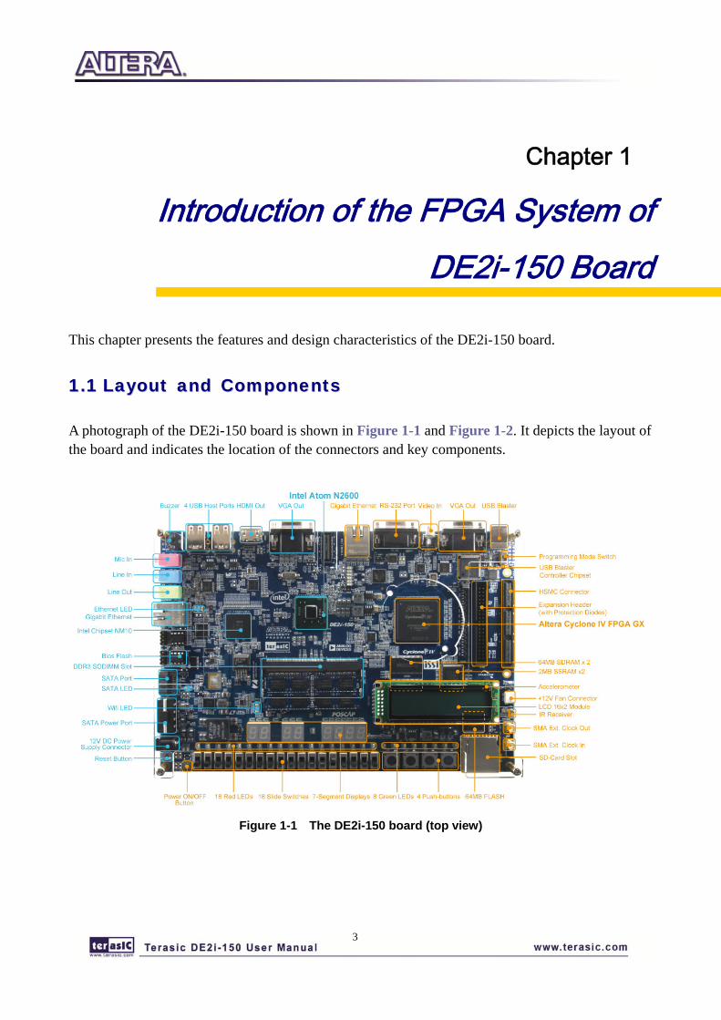
A photograph of the DE2i-150 board is shown in Figure 1-1 and Figure 1-2. It depicts the layout of the board and indicates the location of the connectors and key components.
Figure 1-1 The DE2i-150 board (top view)
4
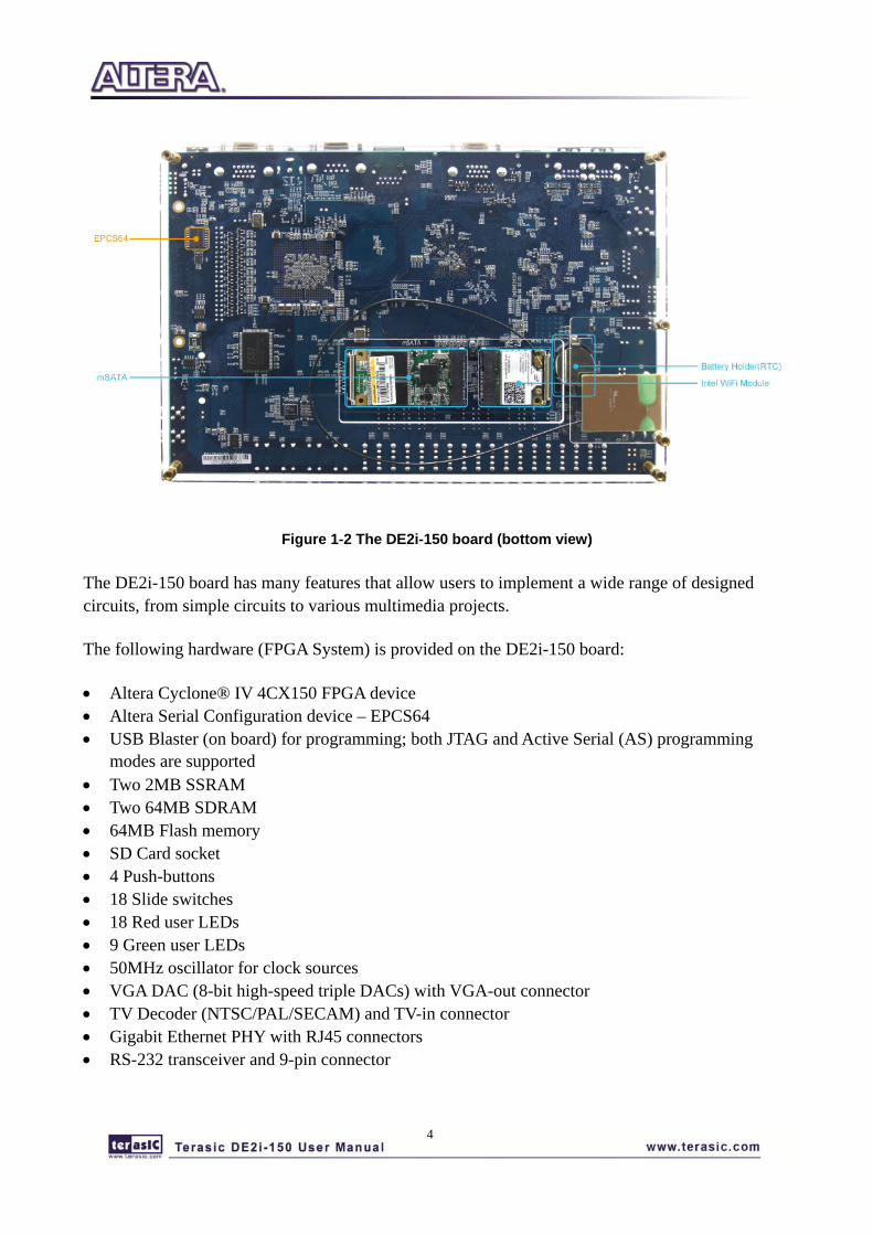
Figure 1-2 The DE2i-150 board (bottom view)
The DE2i-150 board has many features that allow users to implement a wide range of designed circuits, from simple circuits to various multimedia projects.
The following hardware (FPGA System) is provided on the DE2i-150 board:
• Altera Cyclone® IV 4CX150 FPGA device • Altera Serial Configuration device – EPCS64 • USB Blaster (on board) for programming; both JTAG and Active Serial (AS) programming
modes are supported • Two 2MB SSRAM • Two 64MB SDRAM • 64MB Flash memory • SD Card socket • 4 Push-buttons • 18 Slide switches • 18 Red user LEDs • 9 Green user LEDs • 50MHz oscillator for clock sources • VGA DAC (8-bit high-speed triple DACs) with VGA-out connector • TV Decoder (NTSC/PAL/SECAM) and TV-in connector • Gigabit Ethernet PHY with RJ45 connectors • RS-232 transceiver and 9-pin connector
5
• IR Receiver • 2 SMA connectors for external clock input/output • One 40-pin Expansion Header with diode protection • One High Speed Mezzanine Card (HSMC) connector • 16x2 LCD module
In addition to these hardware features, the DE2i-150 board has software support for standard I/O interfaces and a control panel facility for accessing various components. Also, the software is provided for supporting a number of demonstrations that illustrate the advanced capabilities of the DE2i-150 board.
In order to use the DE2i-150 board, the user has to be familiar with the Quartus II software. The necessary knowledge can be acquired by reading the tutorials “My_First_Fpga”. These tutorials are provided in the directory DE2i_150_tutorials on the DE2i-150 System CD that accompanies the DE2i-150 kit and can also be found on Terasic’s DE2i-150 web pages.
11..22 BBlloocckk DDiiaaggrraamm ooff tthhee DDEE22ii--115500 BBooaarrdd
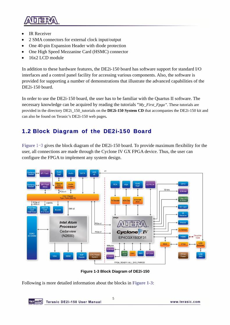
Figure 1-3 gives the block diagram of the DE2i-150 board. To provide maximum flexibility for the user, all connections are made through the Cyclone IV GX FPGA device. Thus, the user can configure the FPGA to implement any system design.
Figure 1-3 Block Diagram of DE2i-150
Following is more detailed information about the blocks in Figure 1-3:
6
FFPPGGAA ddeevviiccee o Cyclone IV EP4CGX150DF31 device o 149,760 LEs o 720 M9K memory blocks o 6,480 Kbits embedded memory o 8 PLLs
FFPPGGAA ccoonnffiigguurraattiioonn o JTAG and AS mode configuration o EPCS64 serial configuration device o On-board USB Blaster circuitry
MMeemmoorryy ddeevviicceess o 128MB (32Mx32bit) SDRAM o 4MB (1Mx32) SSRAM o 64MB (4Mx16) Flash with 16-bit mode
SSDD CCaarrdd ssoocckkeett o Provides SPI and 4-bit SD mode for SD Card access
CCoonnnneeccttoorrss o Ethernet 10/100/1000 Mbps ports o High Speed Mezzanine Card (HSMC) o 40-pin expansion port o VGA-out connector o VGA DAC (high speed triple DACs) o DB9 serial connector for RS-232 port with flow control
CClloocckk o Three 50MHz oscillator clock inputs o SMA connectors (external clock input/output)
DDiissppllaayy o 16x2 LCD module
7
SSwwiittcchheess aanndd iinnddiiccaattoorrss o 18 slide switches and 4 push-buttons switches o 18 red and 9 green LEDs o Eight 7-segment displays
OOtthheerr ffeeaattuurreess o Infrared remote-control receiver module o TV decoder (NTSC/PAL/SECAM) and TV-in connector

8
Chapter 2 DE2i-150 Control Panel
The DE2i-150 board comes with a Control Panel program that allows users to access various components on the board from a host computer. The host computer communicates with the board through a USB connection. The program can be used to verify the functionality of components on the board or be used as a debug tool while developing RTL code.
This chapter first presents some basic functions of the Control Panel, then describes its structure in block diagram form, and finally describes its capabilities.
22..11 CCoonnttrrooll PPaanneell SSeettuupp
The Control Panel Software Utility is located in the directory “Tools/ ControlPanel” in the DE2i-150 System CD. It's free of installation, just copy the whole folder to your host computer and launch the control panel by executing the “DE2i_150_ControlPanel.exe”.
Specific control circuits should be downloaded to your FPGA board before the control panel can request it to perform required tasks. The program will call Quartus II tools to download the control circuit to the FPGA board through USB-Blaster[USB-0] connection.
To activate the Control Panel, perform the following steps:
1. Make sure Quartus II 12.1 or later version is installed successfully on your PC.
2. Set the RUN/PROG switch to the RUN position.
3. Connect the supplied USB cable to the USB Blaster port, connect the 12V power supply, and turn the power switch ON.
4. Start the executable DE2i_150_ControlPanel.exe on the host computer. The Control Panel user interface shown in Figure 2-1 will appear.
5. The DE2i_150_ControlPanel.sof bit stream is loaded automatically as soon as the DE2i_150_control_panel.exe is launched.
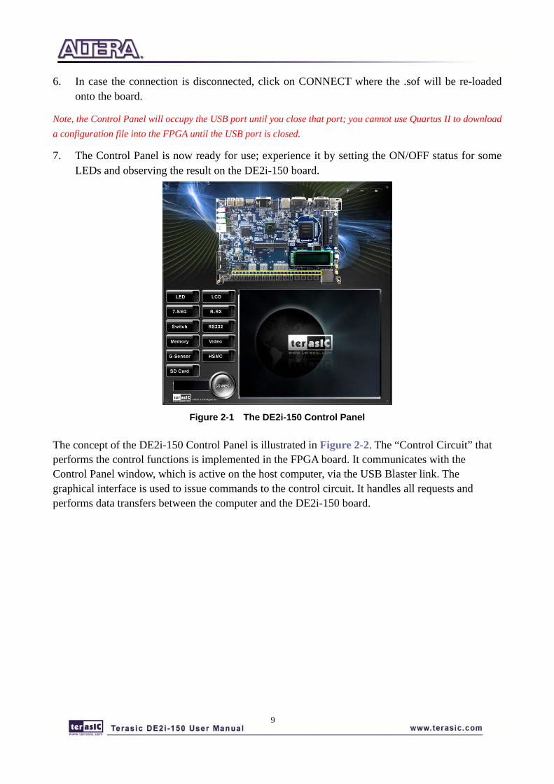
9
6. In case the connection is disconnected, click on CONNECT where the .sof will be re-loaded onto the board.
Note, the Control Panel will occupy the USB port until you close that port; you cannot use Quartus II to download a configuration file into the FPGA until the USB port is closed.
7. The Control Panel is now ready for use; experience it by setting the ON/OFF status for some LEDs and observing the result on the DE2i-150 board.
Figure 2-1 The DE2i-150 Control Panel
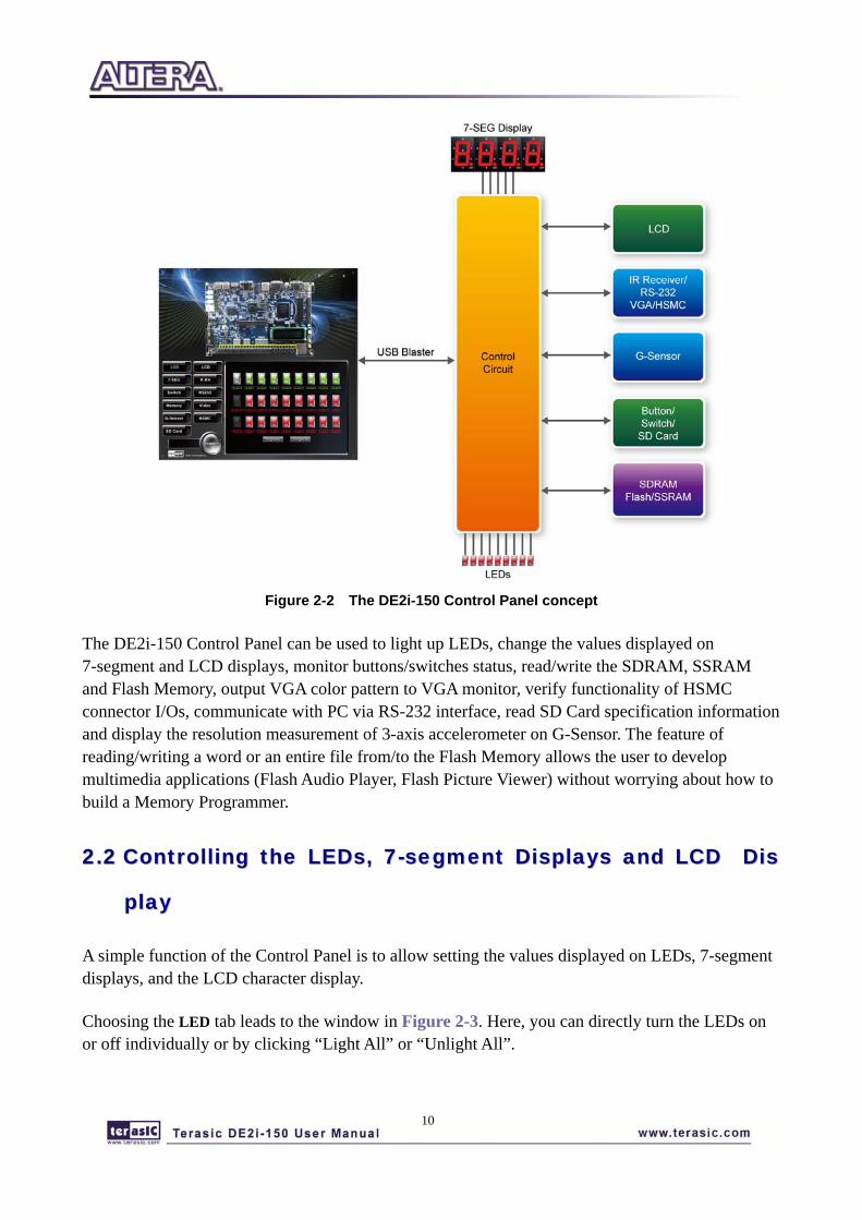
The concept of the DE2i-150 Control Panel is illustrated in Figure 2-2. The “Control Circuit” that performs the control functions is implemented in the FPGA board. It communicates with the Control Panel window, which is active on the host computer, via the USB Blaster link. The graphical interface is used to issue commands to the control circuit. It handles all requests and performs data transfers between the computer and the DE2i-150 board.
10
Figure 2-2 The DE2i-150 Control Panel concept
The DE2i-150 Control Panel can be used to light up LEDs, change the values displayed on 7-segment and LCD displays, monitor buttons/switches status, read/write the SDRAM, SSRAM and Flash Memory, output VGA color pattern to VGA monitor, verify functionality of HSMC connector I/Os, communicate with PC via RS-232 interface, read SD Card specification information and display the resolution measurement of 3-axis accelerometer on G-Sensor. The feature of reading/writing a word or an entire file from/to the Flash Memory allows the user to develop multimedia applications (Flash Audio Player, Flash Picture Viewer) without worrying about how to build a Memory Programmer.
22..22 CCoonnttrroolllliinngg tthhee LLEEDDss,, 77--sseeggmmeenntt DDiissppllaayyss aanndd LLCCDD DDiiss
ppllaayy
A simple function of the Control Panel is to allow setting the values displayed on LEDs, 7-segment displays, and the LCD character display.
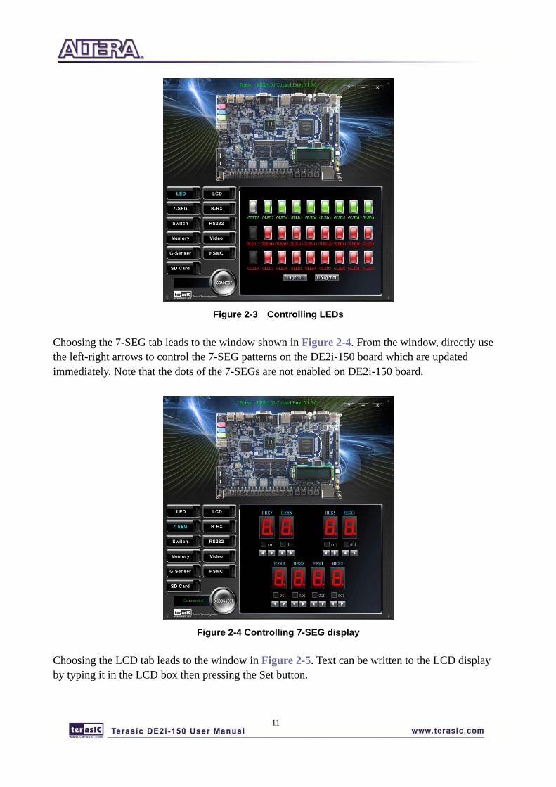
Choosing the LED tab leads to the window in Figure 2-3. Here, you can directly turn the LEDs on or off individually or by clicking “Light All” or “Unlight All”.
11
Figure 2-3 Controlling LEDs
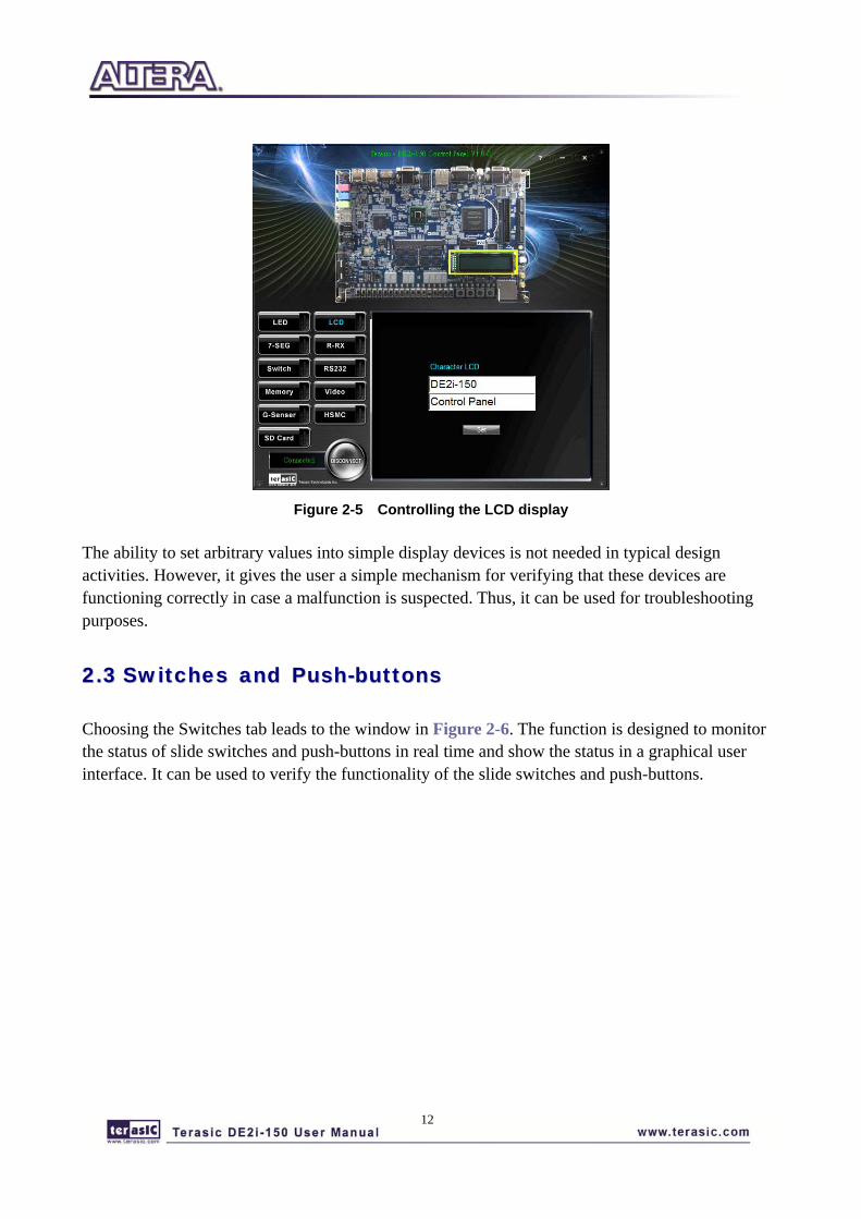
Choosing the 7-SEG tab leads to the window shown in Figure 2-4. From the window, directly use the left-right arrows to control the 7-SEG patterns on the DE2i-150 board which are updated immediately. Note that the dots of the 7-SEGs are not enabled on DE2i-150 board.
Figure 2-4 Controlling 7-SEG display
Choosing the LCD tab leads to the window in Figure 2-5. Text can be written to the LCD display by typing it in the LCD box then pressing the Set button.
12
Figure 2-5 Controlling the LCD display
The ability to set arbitrary values into simple display devices is not needed in typical design activities. However, it gives the user a simple mechanism for verifying that these devices are functioning correctly in case a malfunction is suspected. Thus, it can be used for troubleshooting purposes.
22..33 SSwwiittcchheess aanndd PPuusshh--bbuuttttoonnss
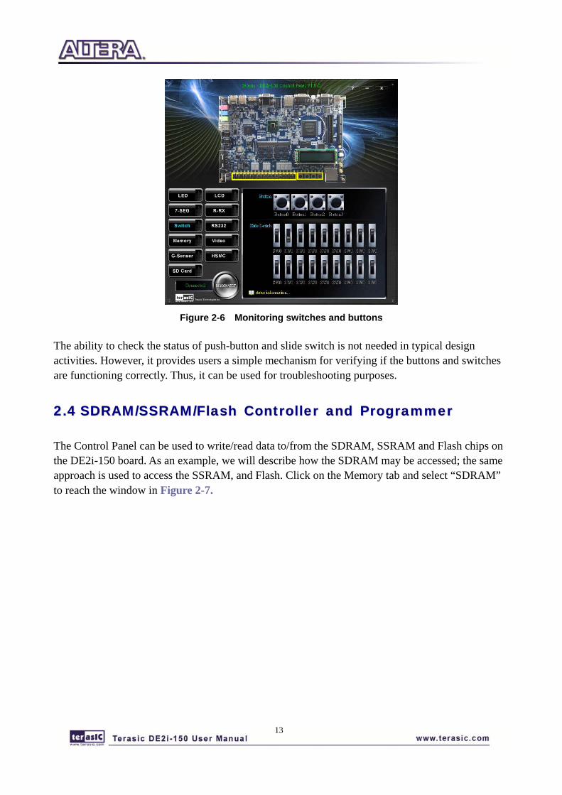
Choosing the Switches tab leads to the window in Figure 2-6. The function is designed to monitor the status of slide switches and push-buttons in real time and show the status in a graphical user interface. It can be used to verify the functionality of the slide switches and push-buttons.
13
Figure 2-6 Monitoring switches and buttons
The ability to check the status of push-button and slide switch is not needed in typical design activities. However, it provides users a simple mechanism for verifying if the buttons and switches are functioning correctly. Thus, it can be used for troubleshooting purposes.
22..44 SSDDRRAAMM//SSSSRRAAMM//FFllaasshh CCoonnttrroolllleerr aanndd PPrrooggrraammmmeerr
The Control Panel can be used to write/read data to/from the SDRAM, SSRAM and Flash chips on the DE2i-150 board. As an example, we will describe how the SDRAM may be accessed; the same approach is used to access the SSRAM, and Flash. Click on the Memory tab and select “SDRAM” to reach the window in Figure 2-7.

14
Figure 2-7 Accessing the SDRAM
A 16-bit word can be written into the SDRAM by entering the address of the desired location, specifying the data to be written, and pressing the Write button. Contents of the location can be read by pressing the Read button. Figure 2-7 depicts the result of writing the hexadecimal value 06CA into offset address 200, followed by reading the same location.
The Sequential Write function of the Control Panel is used to write the contents of a file into the SDRAM as follows:
1. Specify the starting address in the Address box.
2. Specify the number of bytes to be written in the Length box. If the entire file is to be loaded, then a checkmark may be placed in the File Length box instead of giving the number of bytes.
3. To initiate the writing process, click on the Write a File to Memory button.
4. When the Control Panel responds with the standard Windows dialog box asking for the source file, specify the desired file in the usual manner.
The Control Panel also supports loading files with a .hex extension. Files with a .hex extension are ASCII text files that specify memory values using ASCII characters to represent hexadecimal values. For example, a file containing the line
0123456789ABCDEF
Defines eight 8-bit values: 01, 23, 45, 67, 89, AB, CD, EF. These values will be loaded consecutively into the memory.
15
The Sequential Read function is used to read the contents of the SDRAM and fill them into a file as follows:
1. Specify the starting address in the Address box.
2. Specify the number of bytes to be copied into the file in the Length box. If the entire contents of the SDRAM are to be copied (which involves all 128 Mbytes), then place a checkmark in the Entire Memory box.
3. Press Load Memory Content to a File button.
4. When the Control Panel responds with the standard Windows dialog box asking for the destination file, specify the desired file in the usual manner.
Users can use the similar way to access the SSRAM and Flash. Please note that users need to erase the Flash before writing data to it.
22..55 SSDD CCaarrdd
The function is designed to read the identification and specification information of the SD Card. The 4-bit SD MODE is used to access the SD Card. This function can be used to verify the functionality of the SD Card Interface. Follow the steps below to exercise the SD Card:
1. Choosing the SD Card tab leads to the window in Figure 2-8.
2. Insert an SD Card to the DE2i-150 board, and then press the Read button to read the SD Card. The SD Card’s identification, specification, and file format information will be displayed in the control window.
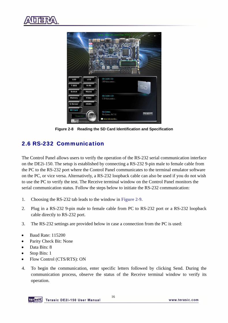
16
Figure 2-8 Reading the SD Card Identification and Specification
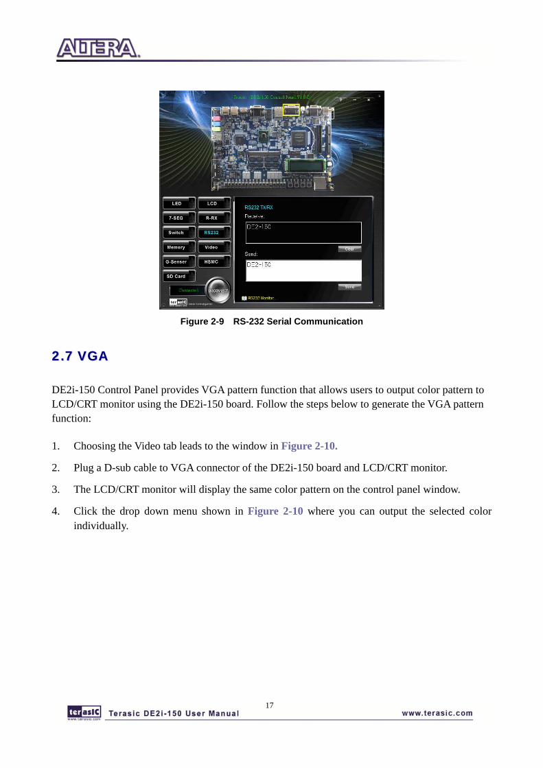
22..66 RRSS--223322 CCoommmmuunniiccaattiioonn
The Control Panel allows users to verify the operation of the RS-232 serial communication interface on the DE2i-150. The setup is established by connecting a RS-232 9-pin male to female cable from the PC to the RS-232 port where the Control Panel communicates to the terminal emulator software on the PC, or vice versa. Alternatively, a RS-232 loopback cable can also be used if you do not wish to use the PC to verify the test. The Receive terminal window on the Control Panel monitors the serial communication status. Follow the steps below to initiate the RS-232 communication:
1. Choosing the RS-232 tab leads to the window in Figure 2-9.
2. Plug in a RS-232 9-pin male to female cable from PC to RS-232 port or a RS-232 loopback cable directly to RS-232 port.
3. The RS-232 settings are provided below in case a connection from the PC is used:
• Baud Rate: 115200 • Parity Check Bit: None • Data Bits: 8 • Stop Bits: 1 • Flow Control (CTS/RTS): ON
4. To begin the communication, enter specific letters followed by clicking Send. During the communication process, observe the status of the Receive terminal window to verify its operation.
17
Figure 2-9 RS-232 Serial Communication
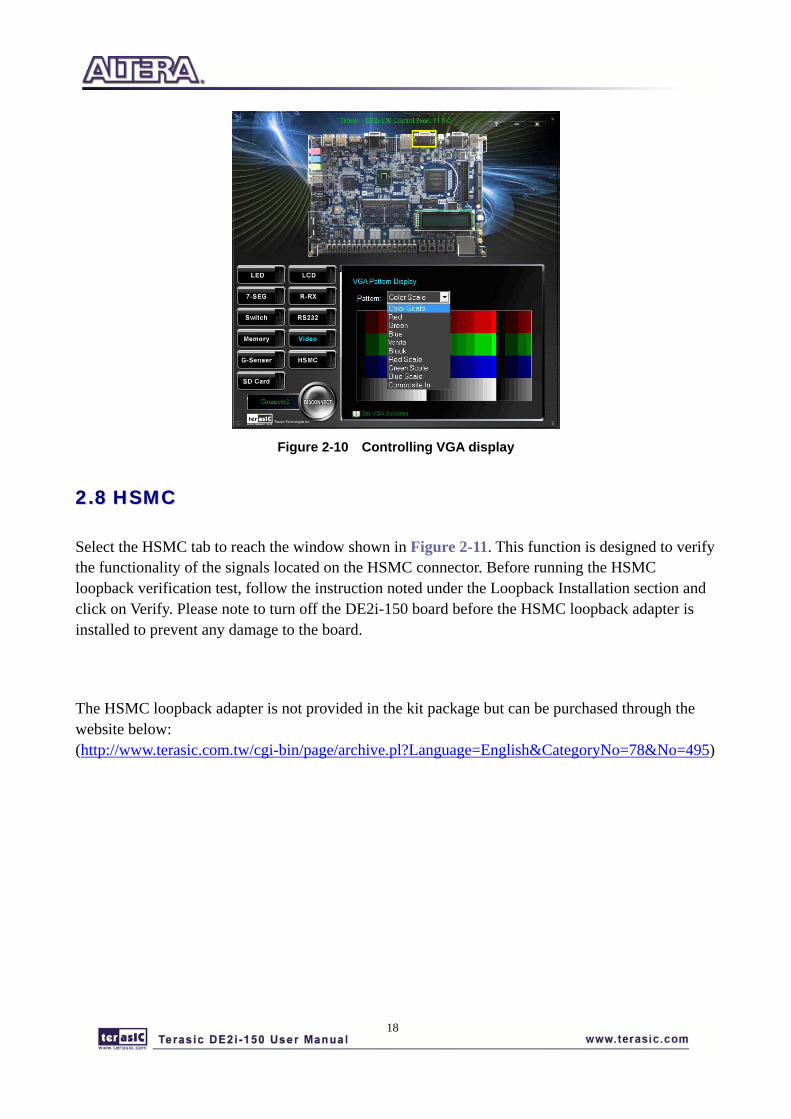
22..77 VVGGAA
DE2i-150 Control Panel provides VGA pattern function that allows users to output color pattern to LCD/CRT monitor using the DE2i-150 board. Follow the steps below to generate the VGA pattern function:
1. Choosing the Video tab leads to the window in Figure 2-10.
2. Plug a D-sub cable to VGA connector of the DE2i-150 board and LCD/CRT monitor.
3. The LCD/CRT monitor will display the same color pattern on the control panel window.
4. Click the drop down menu shown in Figure 2-10 where you can output the selected color individually.
18
Figure 2-10 Controlling VGA display
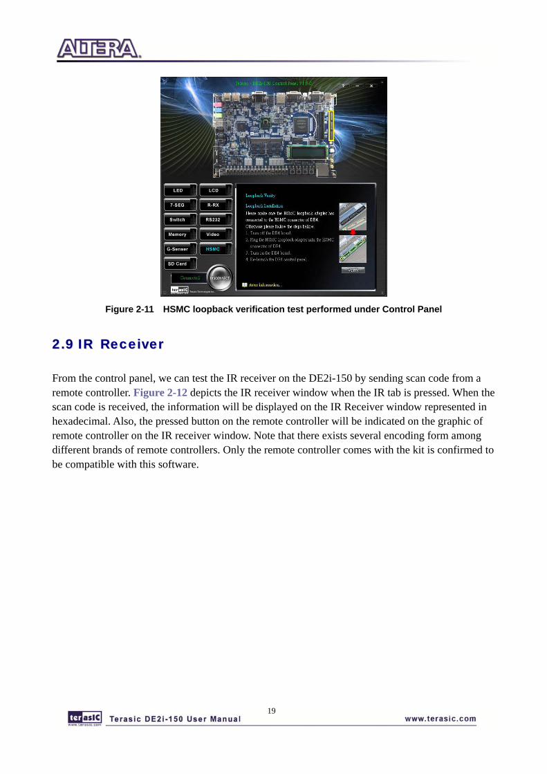
22..88 HHSSMMCC
Select the HSMC tab to reach the window shown in Figure 2-11. This function is designed to verify the functionality of the signals located on the HSMC connector. Before running the HSMC loopback verification test, follow the instruction noted under the Loopback Installation section and click on Verify. Please note to turn off the DE2i-150 board before the HSMC loopback adapter is installed to prevent any damage to the board.
The HSMC loopback adapter is not provided in the kit package but can be purchased through the website below: (http://www.terasic.com.tw/cgi-bin/page/archive.pl?Language=English&CategoryNo=78&No=495)
19
Figure 2-11 HSMC loopback verification test performed under Control Panel
22..99 IIRR RReecceeiivveerr
From the control panel, we can test the IR receiver on the DE2i-150 by sending scan code from a remote controller. Figure 2-12 depicts the IR receiver window when the IR tab is pressed. When the scan code is received, the information will be displayed on the IR Receiver window represented in hexadecimal. Also, the pressed button on the remote controller will be indicated on the graphic of remote controller on the IR receiver window. Note that there exists several encoding form among different brands of remote controllers. Only the remote controller comes with the kit is confirmed to be compatible with this software.
20
Figure 2-12 Testing the IR receiver using remote controller
22..1100 GG--SSeennssoorr
On the DE2i-150 board, the G-sensor function is being demonstrated by Spirit level .The user can rotate the DE2i-150 board to different direction, up or down, left or right. The bubble will travel quickly following your manners. Meanwhile, the control panel will show the accelerated data in x-axis, y-axis and z-axis as shown in Figure 2-12.
Note that the resolution measurement of 3-axis accelerometer is set to +- 2g
21
Figure 2-13 Testing the G-sensor
22..1111 OOvveerraallll SSttrruuccttuurree ooff tthhee DDEE22ii--115500 CCoonnttrrooll PPaanneell
The DE2i-150 Control Panel is based on a Nios II SOPC system instantiated in the Cyclone IV GX FPGA with software running on the on-chip memory. The software part is implemented in C code; the hardware part is implemented in Verilog HDL code with SOPC builder. The source code is not available on the DE2i_150 System CD.
To run the Control Panel, users should make the configuration according to Section 3.1. Figure 2-14 depicts the structure of the Control Panel. Each input/output device is controlled by the Nios II Processor instantiated in the FPGA chip. The communication with the PC is done via the USB Blaster link. The Nios II interprets the commands sent from the PC and performs the corresponding actions.
22
Figure 2-14 The block diagram of the DE2i-150 control panel
23
Chapter 3 Using the DE2i-150 Board
This chapter gives instructions for using the DE2i-150 board and describes each of its peripherals.
33..11 MMoonniittoorr FFuunnccttiioonn ffoorr tthhee SSttaattuuss ooff FFPPGGAA CCoonnffiigguurraattiioonn
In the DE2i-150 power up sequence, there is a monitor circuit that monitors the status of the FPGA configuration. After it confirms the configuration is complete, the power up sequence will go to next state. If the configuration is not complete, the CPU will not initiate.
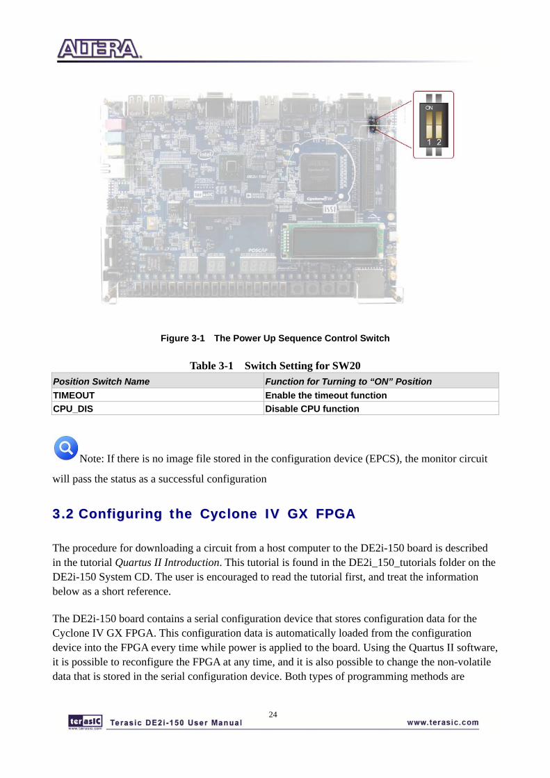
There is a 2-position dip-switch (SW20, as shown in Figure 3.1) on this circuit, which can be used for two settings.
The first switch configures TIMEOUT, which sets a timer in the monitor circuit to ignore any FPGA configuration failure. When the counter goes to the set value, the power up sequence state continue powering up the CPU regardless of whether the FPGA has not been configured normally or not.
The second switch position configures CPU_DIS, which disables CPU power up.
Table 3-1 shows the detailed setting for SW20.
24
Figure 3-1 The Power Up Sequence Control Switch
Table 3-1 Switch Setting for SW20 Position Switch Name Function for Turning to “ON” Position TIMEOUT Enable the timeout function CPU_DIS Disable CPU function
Note: If there is no image file stored in the configuration device (EPCS), the monitor circuit
will pass the status as a successful configuration
33..22 CCoonnffiigguurriinngg tthhee CCyycclloonnee IIVV GGXX FFPPGGAA
The procedure for downloading a circuit from a host computer to the DE2i-150 board is described in the tutorial Quartus II Introduction. This tutorial is found in the DE2i_150_tutorials folder on the DE2i-150 System CD. The user is encouraged to read the tutorial first, and treat the information below as a short reference.
The DE2i-150 board contains a serial configuration device that stores configuration data for the Cyclone IV GX FPGA. This configuration data is automatically loaded from the configuration device into the FPGA every time while power is applied to the board. Using the Quartus II software, it is possible to reconfigure the FPGA at any time, and it is also possible to change the non-volatile data that is stored in the serial configuration device. Both types of programming methods are
25
described below.
1. JTAG programming: In this method of programming, named after the IEEE standards Joint Test Action Group, the configuration bit stream is downloaded directly into the Cyclone IV GX FPGA. The FPGA will retain this configuration as long as power is applied to the board; the configuration information will be lost when the power is turned off.
2. AS programming: In this method, called Active Serial programming, the configuration bit stream is downloaded into the Altera EPCS64 serial configuration device. It provides non-volatile storage of the bit stream, so that the information is retained even when the power supply to the DE2i-150 board is turned off. When the board’s power is turned on, the configuration data in the EPCS64 device is automatically loaded into the Cyclone IV GX FPGA.
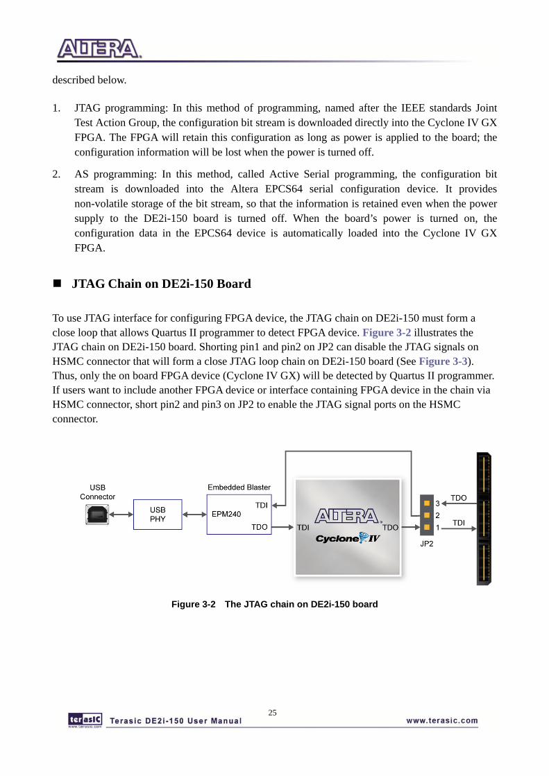
JTAG Chain on DE2i-150 Board
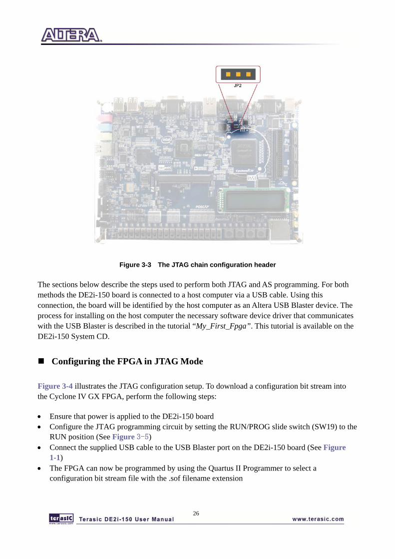
To use JTAG interface for configuring FPGA device, the JTAG chain on DE2i-150 must form a close loop that allows Quartus II programmer to detect FPGA device. Figure 3-2 illustrates the JTAG chain on DE2i-150 board. Shorting pin1 and pin2 on JP2 can disable the JTAG signals on HSMC connector that will form a close JTAG loop chain on DE2i-150 board (See Figure 3-3). Thus, only the on board FPGA device (Cyclone IV GX) will be detected by Quartus II programmer. If users want to include another FPGA device or interface containing FPGA device in the chain via HSMC connector, short pin2 and pin3 on JP2 to enable the JTAG signal ports on the HSMC connector.
Figure 3-2 The JTAG chain on DE2i-150 board
26
Figure 3-3 The JTAG chain configuration header
The sections below describe the steps used to perform both JTAG and AS programming. For both methods the DE2i-150 board is connected to a host computer via a USB cable. Using this connection, the board will be identified by the host computer as an Altera USB Blaster device. The process for installing on the host computer the necessary software device driver that communicates with the USB Blaster is described in the tutorial “My_First_Fpga”. This tutorial is available on the DE2i-150 System CD.
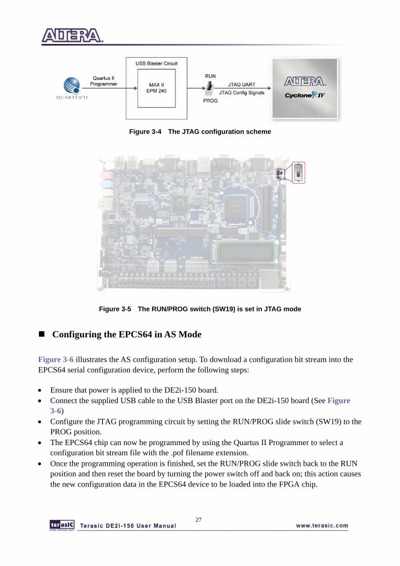
Configuring the FPGA in JTAG Mode
Figure 3-4 illustrates the JTAG configuration setup. To download a configuration bit stream into the Cyclone IV GX FPGA, perform the following steps:
• Ensure that power is applied to the DE2i-150 board • Configure the JTAG programming circuit by setting the RUN/PROG slide switch (SW19) to the
RUN position (See Figure 3-5) • Connect the supplied USB cable to the USB Blaster port on the DE2i-150 board (See Figure
1-1) • The FPGA can now be programmed by using the Quartus II Programmer to select a
configuration bit stream file with the .sof filename extension
27
Figure 3-4 The JTAG configuration scheme
Figure 3-5 The RUN/PROG switch (SW19) is set in JTAG mode
Configuring the EPCS64 in AS Mode
Figure 3-6 illustrates the AS configuration setup. To download a configuration bit stream into the EPCS64 serial configuration device, perform the following steps:
• Ensure that power is applied to the DE2i-150 board. • Connect the supplied USB cable to the USB Blaster port on the DE2i-150 board (See Figure
3-6) • Configure the JTAG programming circuit by setting the RUN/PROG slide switch (SW19) to the
PROG position. • The EPCS64 chip can now be programmed by using the Quartus II Programmer to select a
configuration bit stream file with the .pof filename extension. • Once the programming operation is finished, set the RUN/PROG slide switch back to the RUN
position and then reset the board by turning the power switch off and back on; this action causes the new configuration data in the EPCS64 device to be loaded into the FPGA chip.
28
Figure 3-6 The AS configuration scheme
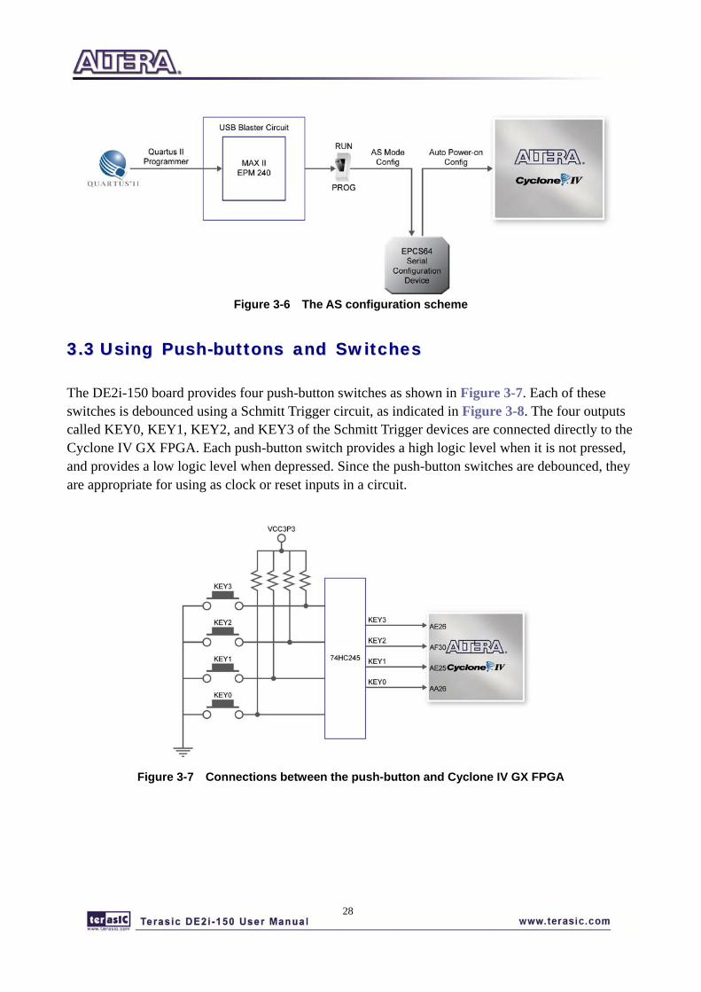
33..33 UUssiinngg PPuusshh--bbuuttttoonnss aanndd SSwwiittcchheess
The DE2i-150 board provides four push-button switches as shown in Figure 3-7. Each of these switches is debounced using a Schmitt Trigger circuit, as indicated in Figure 3-8. The four outputs called KEY0, KEY1, KEY2, and KEY3 of the Schmitt Trigger devices are connected directly to the Cyclone IV GX FPGA. Each push-button switch provides a high logic level when it is not pressed, and provides a low logic level when depressed. Since the push-button switches are debounced, they are appropriate for using as clock or reset inputs in a circuit.
Figure 3-7 Connections between the push-button and Cyclone IV GX FPGA
29
Pushbutton releasedPushbutton depressed
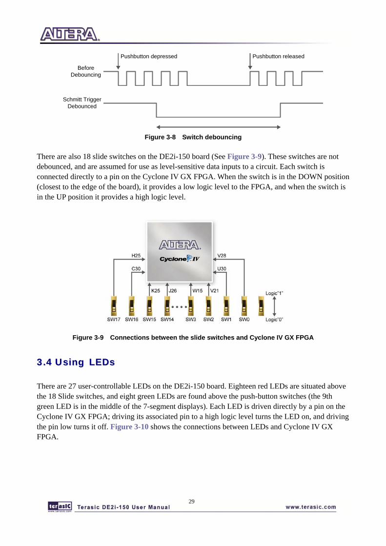
BeforeDebouncing
Schmitt TriggerDebounced
Figure 3-8 Switch debouncing
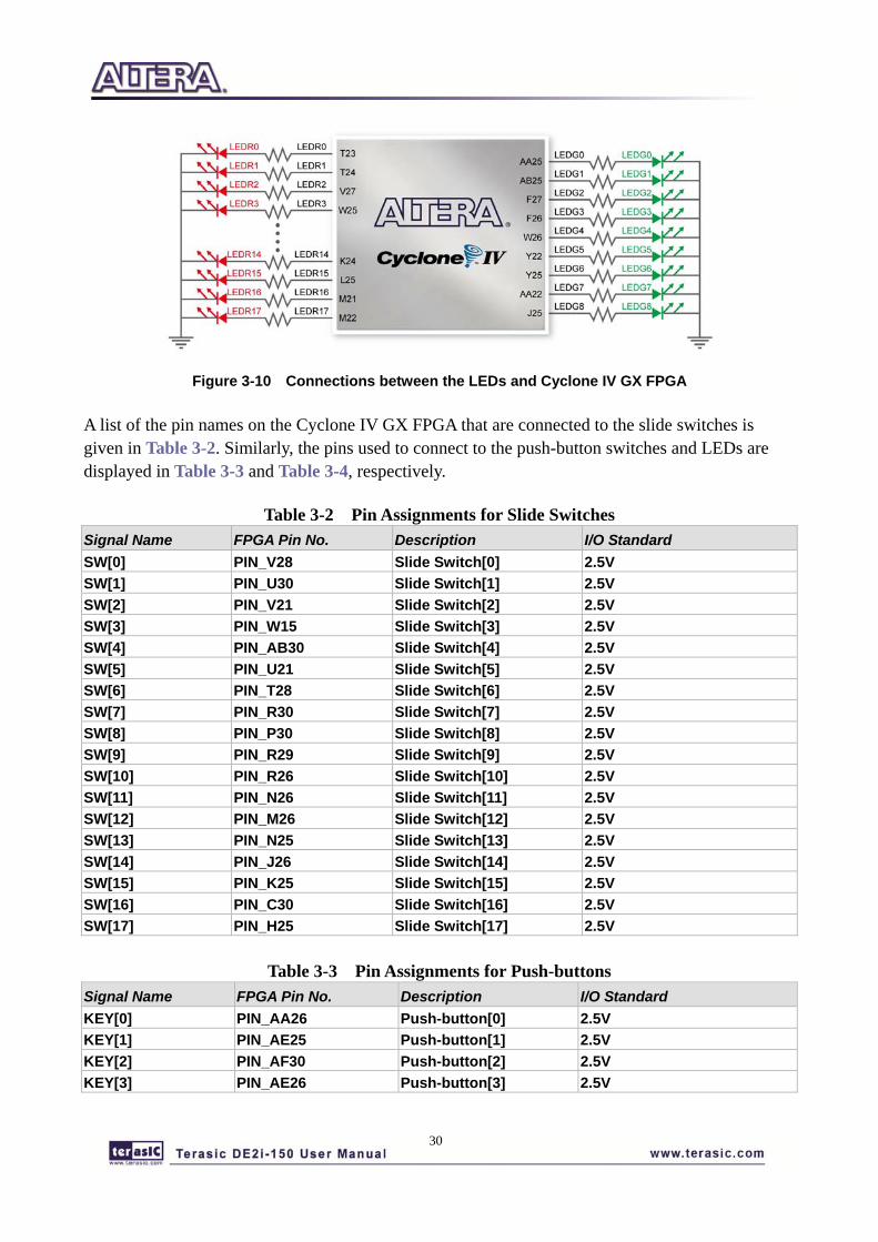
There are also 18 slide switches on the DE2i-150 board (See Figure 3-9). These switches are not debounced, and are assumed for use as level-sensitive data inputs to a circuit. Each switch is connected directly to a pin on the Cyclone IV GX FPGA. When the switch is in the DOWN position (closest to the edge of the board), it provides a low logic level to the FPGA, and when the switch is in the UP position it provides a high logic level.
Figure 3-9 Connections between the slide switches and Cyclone IV GX FPGA
33..44 UUssiinngg LLEEDDss
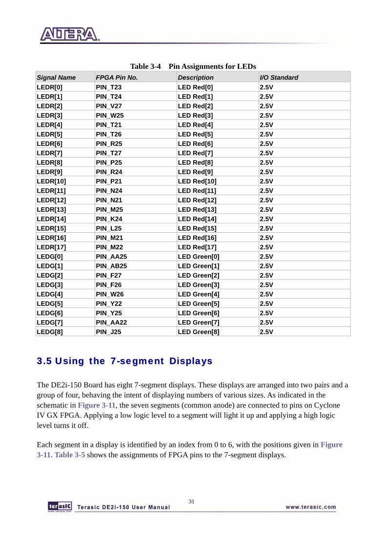
There are 27 user-controllable LEDs on the DE2i-150 board. Eighteen red LEDs are situated above the 18 Slide switches, and eight green LEDs are found above the push-button switches (the 9th green LED is in the middle of the 7-segment displays). Each LED is driven directly by a pin on the Cyclone IV GX FPGA; driving its associated pin to a high logic level turns the LED on, and driving the pin low turns it off. Figure 3-10 shows the connections between LEDs and Cyclone IV GX FPGA.
30
Figure 3-10 Connections between the LEDs and Cyclone IV GX FPGA
A list of the pin names on the Cyclone IV GX FPGA that are connected to the slide switches is given in Table 3-2. Similarly, the pins used to connect to the push-button switches and LEDs are displayed in Table 3-3 and Table 3-4, respectively.
Table 3-2 Pin Assignments for Slide Switches Signal Name FPGA Pin No. Description I/O Standard SW[0] PIN_V28 Slide Switch[0] 2.5V SW[1] PIN_U30 Slide Switch[1] 2.5V SW[2] PIN_V21 Slide Switch[2] 2.5V SW[3] PIN_W15 Slide Switch[3] 2.5V SW[4] PIN_AB30 Slide Switch[4] 2.5V SW[5] PIN_U21 Slide Switch[5] 2.5V SW[6] PIN_T28 Slide Switch[6] 2.5V SW[7] PIN_R30 Slide Switch[7] 2.5V SW[8] PIN_P30 Slide Switch[8] 2.5V SW[9] PIN_R29 Slide Switch[9] 2.5V SW[10] PIN_R26 Slide Switch[10] 2.5V SW[11] PIN_N26 Slide Switch[11] 2.5V SW[12] PIN_M26 Slide Switch[12] 2.5V SW[13] PIN_N25 Slide Switch[13] 2.5V SW[14] PIN_J26 Slide Switch[14] 2.5V SW[15] PIN_K25 Slide Switch[15] 2.5V SW[16] PIN_C30 Slide Switch[16] 2.5V SW[17] PIN_H25 Slide Switch[17] 2.5V
Table 3-3 Pin Assignments for Push-buttons
Signal Name FPGA Pin No. Description I/O Standard KEY[0] PIN_AA26 Push-button[0] 2.5V KEY[1] PIN_AE25 Push-button[1] 2.5V KEY[2] PIN_AF30 Push-button[2] 2.5V KEY[3] PIN_AE26 Push-button[3] 2.5V
31
Table 3-4 Pin Assignments for LEDs
Signal Name FPGA Pin No. Description I/O Standard LEDR[0] PIN_T23 LED Red[0] 2.5V LEDR[1] PIN_T24 LED Red[1] 2.5V LEDR[2] PIN_V27 LED Red[2] 2.5V LEDR[3] PIN_W25 LED Red[3] 2.5V LEDR[4] PIN_T21 LED Red[4] 2.5V LEDR[5] PIN_T26 LED Red[5] 2.5V LEDR[6] PIN_R25 LED Red[6] 2.5V LEDR[7] PIN_T27 LED Red[7] 2.5V LEDR[8] PIN_P25 LED Red[8] 2.5V LEDR[9] PIN_R24 LED Red[9] 2.5V LEDR[10] PIN_P21 LED Red[10] 2.5V LEDR[11] PIN_N24 LED Red[11] 2.5V LEDR[12] PIN_N21 LED Red[12] 2.5V LEDR[13] PIN_M25 LED Red[13] 2.5V LEDR[14] PIN_K24 LED Red[14] 2.5V LEDR[15] PIN_L25 LED Red[15] 2.5V LEDR[16] PIN_M21 LED Red[16] 2.5V LEDR[17] PIN_M22 LED Red[17] 2.5V LEDG[0] PIN_AA25 LED Green[0] 2.5V LEDG[1] PIN_AB25 LED Green[1] 2.5V LEDG[2] PIN_F27 LED Green[2] 2.5V LEDG[3] PIN_F26 LED Green[3] 2.5V LEDG[4] PIN_W26 LED Green[4] 2.5V LEDG[5] PIN_Y22 LED Green[5] 2.5V LEDG[6] PIN_Y25 LED Green[6] 2.5V LEDG[7] PIN_AA22 LED Green[7] 2.5V LEDG[8] PIN_J25 LED Green[8] 2.5V
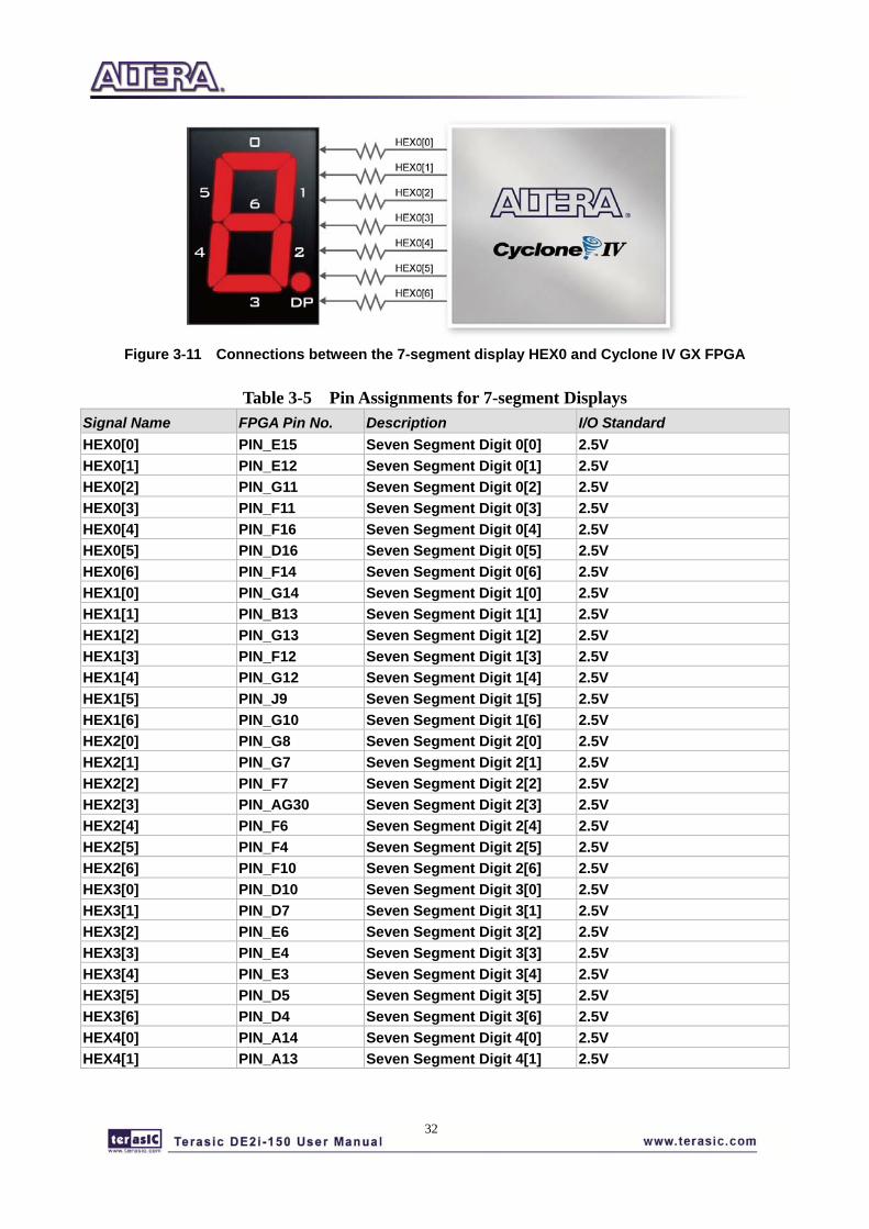
33..55 UUssiinngg tthhee 77--sseeggmmeenntt DDiissppllaayyss
The DE2i-150 Board has eight 7-segment displays. These displays are arranged into two pairs and a group of four, behaving the intent of displaying numbers of various sizes. As indicated in the schematic in Figure 3-11, the seven segments (common anode) are connected to pins on Cyclone IV GX FPGA. Applying a low logic level to a segment will light it up and applying a high logic level turns it off.
Each segment in a display is identified by an index from 0 to 6, with the positions given in Figure 3-11. Table 3-5 shows the assignments of FPGA pins to the 7-segment displays.
32
Figure 3-11 Connections between the 7-segment display HEX0 and Cyclone IV GX FPGA
Table 3-5 Pin Assignments for 7-segment Displays Signal Name FPGA Pin No. Description I/O Standard HEX0[0] PIN_E15 Seven Segment Digit 0[0] 2.5V HEX0[1] PIN_E12 Seven Segment Digit 0[1] 2.5V HEX0[2] PIN_G11 Seven Segment Digit 0[2] 2.5V HEX0[3] PIN_F11 Seven Segment Digit 0[3] 2.5V HEX0[4] PIN_F16 Seven Segment Digit 0[4] 2.5V HEX0[5] PIN_D16 Seven Segment Digit 0[5] 2.5V HEX0[6] PIN_F14 Seven Segment Digit 0[6] 2.5V HEX1[0] PIN_G14 Seven Segment Digit 1[0] 2.5V HEX1[1] PIN_B13 Seven Segment Digit 1[1] 2.5V HEX1[2] PIN_G13 Seven Segment Digit 1[2] 2.5V HEX1[3] PIN_F12 Seven Segment Digit 1[3] 2.5V HEX1[4] PIN_G12 Seven Segment Digit 1[4] 2.5V HEX1[5] PIN_J9 Seven Segment Digit 1[5] 2.5V HEX1[6] PIN_G10 Seven Segment Digit 1[6] 2.5V HEX2[0] PIN_G8 Seven Segment Digit 2[0] 2.5V HEX2[1] PIN_G7 Seven Segment Digit 2[1] 2.5V HEX2[2] PIN_F7 Seven Segment Digit 2[2] 2.5V HEX2[3] PIN_AG30 Seven Segment Digit 2[3] 2.5V HEX2[4] PIN_F6 Seven Segment Digit 2[4] 2.5V HEX2[5] PIN_F4 Seven Segment Digit 2[5] 2.5V HEX2[6] PIN_F10 Seven Segment Digit 2[6] 2.5V HEX3[0] PIN_D10 Seven Segment Digit 3[0] 2.5V HEX3[1] PIN_D7 Seven Segment Digit 3[1] 2.5V HEX3[2] PIN_E6 Seven Segment Digit 3[2] 2.5V HEX3[3] PIN_E4 Seven Segment Digit 3[3] 2.5V HEX3[4] PIN_E3 Seven Segment Digit 3[4] 2.5V HEX3[5] PIN_D5 Seven Segment Digit 3[5] 2.5V HEX3[6] PIN_D4 Seven Segment Digit 3[6] 2.5V HEX4[0] PIN_A14 Seven Segment Digit 4[0] 2.5V HEX4[1] PIN_A13 Seven Segment Digit 4[1] 2.5V
33
HEX4[2] PIN_C7 Seven Segment Digit 4[2] 2.5V HEX4[3] PIN_C6 Seven Segment Digit 4[3] 2.5V HEX4[4] PIN_C5 Seven Segment Digit 4[4] 2.5V HEX4[5] PIN_C4 Seven Segment Digit 4[5] 2.5V HEX4[6] PIN_C3 Seven Segment Digit 4[6] 2.5V HEX5[0] PIN_D3 Seven Segment Digit 5[0] 2.5V HEX5[1] PIN_A10 Seven Segment Digit 5[1] 2.5V HEX5[2] PIN_A9 Seven Segment Digit 5[2] 2.5V HEX5[3] PIN_A7 Seven Segment Digit 5[3] 2.5V HEX5[4] PIN_A6 Seven Segment Digit 5[4] 2.5V HEX5[5] PIN_A11 Seven Segment Digit 5[5] 2.5V HEX5[6] PIN_B6 Seven Segment Digit 5[6] 2.5V HEX6[0] PIN_B9 Seven Segment Digit 6[0] 2.5V HEX6[1] PIN_B10 Seven Segment Digit 6[1] 2.5V HEX6[2] PIN_C8 Seven Segment Digit 6[2] 2.5V HEX6[3] PIN_C9 Seven Segment Digit 6[3] 2.5V HEX6[4] PIN_D8 Seven Segment Digit 6[4] 2.5V HEX6[5] PIN_D9 Seven Segment Digit 6[5] 2.5V HEX6[6] PIN_E9 Seven Segment Digit 6[6] 2.5V HEX7[0] PIN_E10 Seven Segment Digit 7[0] 2.5V HEX7[1] PIN_F8 Seven Segment Digit 7[1] 2.5V HEX7[2] PIN_F9 Seven Segment Digit 7[2] 2.5V HEX7[3] PIN_C10 Seven Segment Digit 7[3] 2.5V HEX7[4] PIN_C11 Seven Segment Digit 7[4] 2.5V HEX7[5] PIN_C12 Seven Segment Digit 7[5] 2.5V HEX7[6] PIN_D12 Seven Segment Digit 7[6] 2.5V
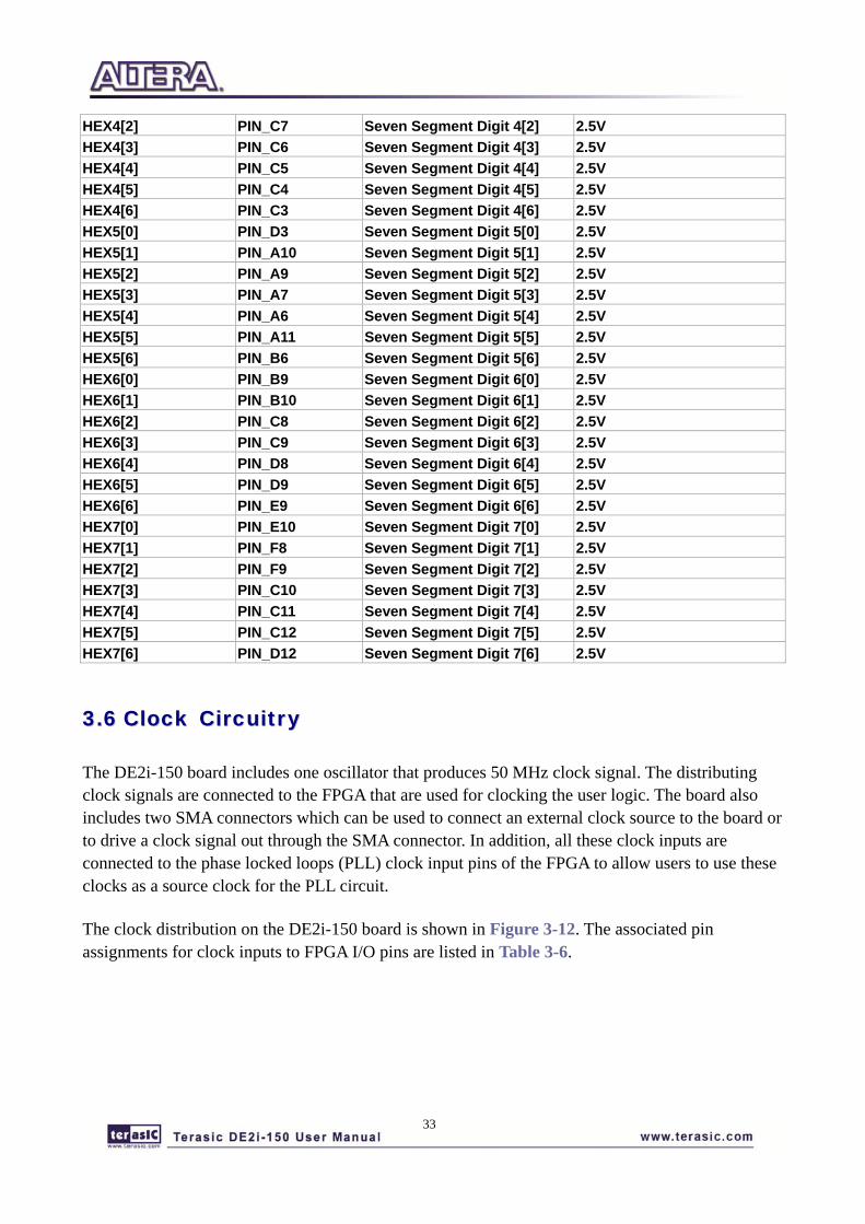
33..66 CClloocckk CCiirrccuuiittrryy
The DE2i-150 board includes one oscillator that produces 50 MHz clock signal. The distributing clock signals are connected to the FPGA that are used for clocking the user logic. The board also includes two SMA connectors which can be used to connect an external clock source to the board or to drive a clock signal out through the SMA connector. In addition, all these clock inputs are connected to the phase locked loops (PLL) clock input pins of the FPGA to allow users to use these clocks as a source clock for the PLL circuit.
The clock distribution on the DE2i-150 board is shown in Figure 3-12. The associated pin assignments for clock inputs to FPGA I/O pins are listed in Table 3-6.
34
Figure 3-12 Block diagram of the clock distribution
Table 3-6 Pin Assignments for Clock Inputs Signal Name FPGA Pin No. Description I/O Standard CLOCK_50 PIN_AJ16 50 MHz clock input 3.3V CLOCK2_50 PIN_A15 50 MHz clock input 3.3V CLOCK3_50 PIN_V15 50 MHz clock input 2.5V SMA_CLKOUT PIN_AF25 External (SMA) clock output 3.3V SMA_CLKIN PIN_AK16 External (SMA) clock input 3.3V
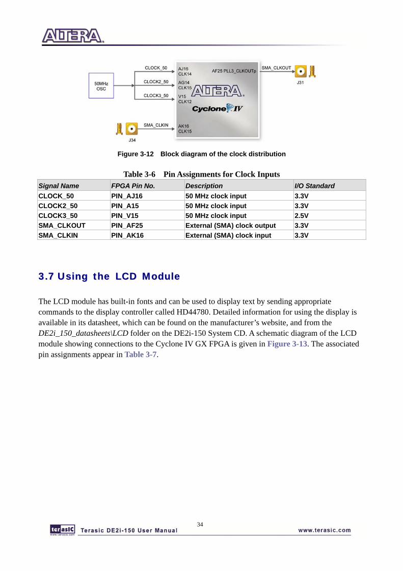
33..77 UUssiinngg tthhee LLCCDD MMoodduullee
The LCD module has built-in fonts and can be used to display text by sending appropriate commands to the display controller called HD44780. Detailed information for using the display is available in its datasheet, which can be found on the manufacturer’s website, and from the DE2i_150_datasheets\LCD folder on the DE2i-150 System CD. A schematic diagram of the LCD module showing connections to the Cyclone IV GX FPGA is given in Figure 3-13. The associated pin assignments appear in Table 3-7.
35
Figure 3-13 Connections between the LCD module and Cyclone IV GX FPGA
Table 3-7 Pin Assignments for LCD Module
Signal Name FPGA Pin No. Description I/O Standard
LCD_DATA[7] PIN_AE4 LCD Data[7] 3.3V LCD_DATA[6] PIN_AH4 LCD Data[6] 3.3V LCD_DATA[5] PIN_AE3 LCD Data[5] 3.3V LCD_DATA[4] PIN_AH2 LCD Data[4] 3.3V LCD_DATA[3] PIN_AE5 LCD Data[3] 3.3V LCD_DATA[2] PIN_AH3 LCD Data[2] 3.3V LCD_DATA[1] PIN_AF3 LCD Data[1] 3.3V LCD_DATA[0] PIN_AG4 LCD Data[0] 3.3V LCD_EN PIN_AF4 LCD Enable 3.3V LCD_RW PIN_AJ3 LCD Read/Write Select, 0 = Write, 1 = Read 3.3V LCD_RS PIN_AG3 LCD Command/Data Select, 0 = Command, 1 = Data 3.3V LCD_ON PIN_AF27 LCD Power ON/OFF 2.5V
33..88 HHiigghh SSppeeeedd MMeezzzzaanniinnee CCaarrdd
The DE2i-150 development board contains a HSMC interface to provide a mechanism for extending the peripheral-set of a FPGA host board by means of add-on cards. This can address today’s high speed signaling requirement as well as low-speed device interface support. The HSMC
36
interface support JTAG, clock outputs and inputs, high speed LVDS and single-ended signaling. The HSMC connector connects directly to the Cyclone IV GX FPGA with 82 pins. Table 3-8 shows the maximum power consumption of the daughter card that connects to HSMC port.
Table 3-8 Power Supply of the HSMC Supplied Voltage Max. Current Limit 12V 1A 3.3V 1.5A
(1).Note the current levels indicated in Table 3-8 are based on 50% resource consumption. If the HSMC
interface is utilized with design resources exceeding 50%, please notify our support ([email protected]). (2). There is a specially note to the J24, which can be used to control the HSMC 12v power supply. If the user sets the J24 in the open status, the output of the HSMC 12V voltage would be cut off.
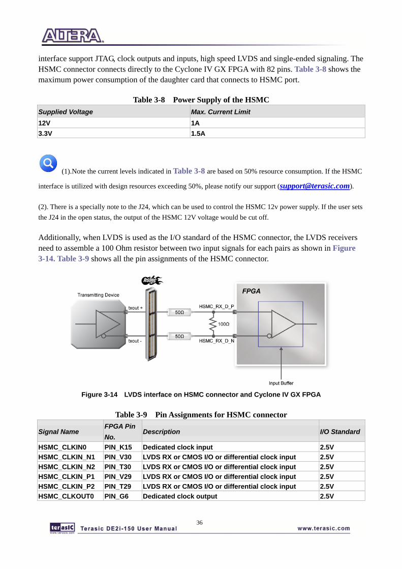
Additionally, when LVDS is used as the I/O standard of the HSMC connector, the LVDS receivers need to assemble a 100 Ohm resistor between two input signals for each pairs as shown in Figure 3-14. Table 3-9 shows all the pin assignments of the HSMC connector.
Figure 3-14 LVDS interface on HSMC connector and Cyclone IV GX FPGA
Table 3-9 Pin Assignments for HSMC connector
Signal Name FPGA Pin No.
Description I/O Standard
HSMC_CLKIN0 PIN_K15 Dedicated clock input 2.5V HSMC_CLKIN_N1 PIN_V30 LVDS RX or CMOS I/O or differential clock input 2.5V HSMC_CLKIN_N2 PIN_T30 LVDS RX or CMOS I/O or differential clock input 2.5V HSMC_CLKIN_P1 PIN_V29 LVDS RX or CMOS I/O or differential clock input 2.5V HSMC_CLKIN_P2 PIN_T29 LVDS RX or CMOS I/O or differential clock input 2.5V HSMC_CLKOUT0 PIN_G6 Dedicated clock output 2.5V
37
HSMC_CLKOUT_N1 PIN_AB28 LVDS TX or CMOS I/O or differential clock input/output 2.5V HSMC_CLKOUT_N2 PIN_Y28 LVDS TX or CMOS I/O or differential clock input/output 2.5V HSMC_CLKOUT_P1 PIN_AB27 LVDS TX or CMOS I/O or differential clock input/output 2.5V HSMC_CLKOUT_P2 PIN_AA28 LVDS TX or CMOS I/O or differential clock input/output 2.5V HSMC_D[0] PIN_AC25 LVDS TX or CMOS I/O 2.5V HSMC_D[1] PIN_E27 LVDS RX or CMOS I/O 2.5V HSMC_D[2] PIN_AB26 LVDS TX or CMOS I/O 2.5V HSMC_D[3] PIN_E28 LVDS RX or CMOS I/O 2.5V HSMC_RX_D_N[0] PIN_G27 LVDS RX bit 0n or CMOS I/O 2.5V HSMC_RX_D_N[1] PIN_G29 LVDS RX bit 1n or CMOS I/O 2.5V HSMC_RX_D_N[2] PIN_H27 LVDS RX bit 2n or CMOS I/O 2.5V HSMC_RX_D_N[3] PIN_K29 LVDS RX bit 3n or CMOS I/O 2.5V HSMC_RX_D_N[4] PIN_L28 LVDS RX bit 4n or CMOS I/O 2.5V HSMC_RX_D_N[5] PIN_M28 LVDS RX bit 5n or CMOS I/O 2.5V HSMC_RX_D_N[6] PIN_N30 LVDS RX bit 6n or CMOS I/O 2.5V HSMC_RX_D_N[7] PIN_P28 LVDS RX bit 7n or CMOS I/O 2.5V HSMC_RX_D_N[8] PIN_R28 LVDS RX bit 8n or CMOS I/O 2.5V HSMC_RX_D_N[9] PIN_U28 LVDS RX bit 9n or CMOS I/O 2.5V HSMC_RX_D_N[10] PIN_W28 LVDS RX bit 10n or CMOS I/O 2.5V HSMC_RX_D_N[11] PIN_W30 LVDS RX bit 11n or CMOS I/O 2.5V HSMC_RX_D_N[12] PIN_M30 LVDS RX bit 12n or CMOS I/O 2.5V HSMC_RX_D_N[13] PIN_Y27 LVDS RX bit 13n or CMOS I/O 2.5V HSMC_RX_D_N[14] PIN_AA29 LVDS RX bit 14n or CMOS I/O 2.5V HSMC_RX_D_N[15] PIN_AD28 LVDS RX bit 15n or CMOS I/O 2.5V HSMC_RX_D_N[16] PIN_AE28 LVDS RX bit 16n or CMOS I/O 2.5V HSMC_RX_D_P[0] PIN_G26 LVDS RX bit 0 or CMOS I/O 2.5V HSMC_RX_D_P[1] PIN_G28 LVDS RX bit 1 or CMOS I/O 2.5V HSMC_RX_D_P[2] PIN_J27 LVDS RX bit 2 or CMOS I/O 2.5V HSMC_RX_D_P[3] PIN_K28 LVDS RX bit 3 or CMOS I/O 2.5V HSMC_RX_D_P[4] PIN_L27 LVDS RX bit 4 or CMOS I/O 2.5V HSMC_RX_D_P[5] PIN_M27 LVDS RX bit 5 or CMOS I/O 2.5V HSMC_RX_D_P[6] PIN_N29 LVDS RX bit 6 or CMOS I/O 2.5V HSMC_RX_D_P[7] PIN_P27 LVDS RX bit 7 or CMOS I/O 2.5V HSMC_RX_D_P[8] PIN_R27 LVDS RX bit 8 or CMOS I/O 2.5V HSMC_RX_D_P[9] PIN_U27 LVDS RX bit 9 or CMOS I/O 2.5V HSMC_RX_D_P[10] PIN_W27 LVDS RX bit 10 or CMOS I/O 2.5V HSMC_RX_D_P[11] PIN_W29 LVDS RX bit 11 or CMOS I/O 2.5V HSMC_RX_D_P[12] PIN_M29 LVDS RX bit 12 or CMOS I/O 2.5V HSMC_RX_D_P[13] PIN_AA27 LVDS RX bit 13 or CMOS I/O 2.5V HSMC_RX_D_P[14] PIN_AB29 LVDS RX bit 14 or CMOS I/O 2.5V HSMC_RX_D_P[15] PIN_AD27 LVDS RX bit 15 or CMOS I/O 2.5V HSMC_RX_D_P[16] PIN_AE27 LVDS RX bit 16 or CMOS I/O 2.5V HSMC_TX_D_N[0] PIN_H28 LVDS TX bit 0n or CMOS I/O 2.5V HSMC_TX_D_N[1] PIN_F29 LVDS TX bit 1n or CMOS I/O 2.5V HSMC_TX_D_N[2] PIN_D30 LVDS TX bit 2n or CMOS I/O 2.5V
38
HSMC_TX_D_N[3] PIN_E30 LVDS TX bit 3n or CMOS I/O 2.5V HSMC_TX_D_N[4] PIN_G30 LVDS TX bit 4n or CMOS I/O 2.5V HSMC_TX_D_N[5] PIN_J30 LVDS TX bit 5n or CMOS I/O 2.5V HSMC_TX_D_N[6] PIN_K27 LVDS TX bit 6n or CMOS I/O 2.5V HSMC_TX_D_N[7] PIN_K30 LVDS TX bit 7n or CMOS I/O 2.5V HSMC_TX_D_N[8] PIN_T25 LVDS TX bit 8n or CMOS I/O 2.5V HSMC_TX_D_N[9] PIN_N28 LVDS TX bit 9n or CMOS I/O 2.5V HSMC_TX_D_N[10] PIN_V26 LVDS TX bit 10n or CMOS I/O 2.5V HSMC_TX_D_N[11] PIN_Y30 LVDS TX bit 11n or CMOS I/O 2.5V HSMC_TX_D_N[12] PIN_AC28 LVDS TX bit 12n or CMOS I/O 2.5V HSMC_TX_D_N[13] PIN_AD30 LVDS TX bit 13n or CMOS I/O 2.5V HSMC_TX_D_N[14] PIN_AE30 LVDS TX bit 14n or CMOS I/O 2.5V HSMC_TX_D_N[15] PIN_AH30 LVDS TX bit 15n or CMOS I/O 2.5V HSMC_TX_D_N[16] PIN_AG29 LVDS TX bit 16n or CMOS I/O 2.5V HSMC_TX_D_P[0] PIN_ J28 LVDS TX bit 0 or CMOS I/O 2.5V HSMC_TX_D_P[1] PIN_ F28 LVDS TX bit 1 or CMOS I/O 2.5V HSMC_TX_D_P[2] PIN_ D29 LVDS TX bit 2 or CMOS I/O 2.5V HSMC_TX_D_P[3] PIN_ F30 LVDS TX bit 3 or CMOS I/O 2.5V HSMC_TX_D_P[4] PIN_ H30 LVDS TX bit 4 or CMOS I/O 2.5V HSMC_TX_D_P[5] PIN_ J29 LVDS TX bit 5 or CMOS I/O 2.5V HSMC_TX_D_P[6] PIN_ K26 LVDS TX bit 6 or CMOS I/O 2.5V HSMC_TX_D_P[7] PIN_ L30 LVDS TX bit 7 or CMOS I/O 2.5V HSMC_TX_D_P[8] PIN_ U25 LVDS TX bit 8 or CMOS I/O 2.5V HSMC_TX_D_P[9] PIN_ N27 LVDS TX bit 9 or CMOS I/O 2.5V HSMC_TX_D_P[10] PIN_ V25 LVDS TX bit 10 or CMOS I/O 2.5V HSMC_TX_D_P[11] PIN_ AA30 LVDS TX bit 11 or CMOS I/O 2.5V HSMC_TX_D_P[12] PIN_ AC27 LVDS TX bit 12 or CMOS I/O 2.5V HSMC_TX_D_P[13] PIN_ AD29 LVDS TX bit 13 or CMOS I/O 2.5V HSMC_TX_D_P[14] PIN_ AE29 LVDS TX bit 14 or CMOS I/O 2.5V HSMC_TX_D_P[15] PIN_ AJ30 LVDS TX bit 15 or CMOS I/O 2.5V HSMC_TX_D_P[16] PIN_ AH29 LVDS TX bit 16 or CMOS I/O 2.5V
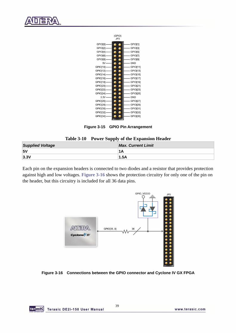
33..99 UUssiinngg tthhee EExxppaannssiioonn HHeeaaddeerr
The DE2i-150 Board provides one 40-pin expansion header. The header connects directly to 36 pins of the Cyclone IV GX FPGA, and also provides DC +5V (VCC5), DC +3.3V (VCC3P3), and two GND pins. Figure 3-15 shows the I/O distribution of the GPIO connector. The maximum power consumption of the daughter card that connects to GPIO port is shown in Table 3-10.
39
Figure 3-15 GPIO Pin Arrangement
Table 3-10 Power Supply of the Expansion Header Supplied Voltage Max. Current Limit 5V 1A 3.3V 1.5A
Each pin on the expansion headers is connected to two diodes and a resistor that provides protection against high and low voltages. Figure 3-16 shows the protection circuitry for only one of the pin on the header, but this circuitry is included for all 36 data pins.
Figure 3-16 Connections between the GPIO connector and Cyclone IV GX FPGA
40
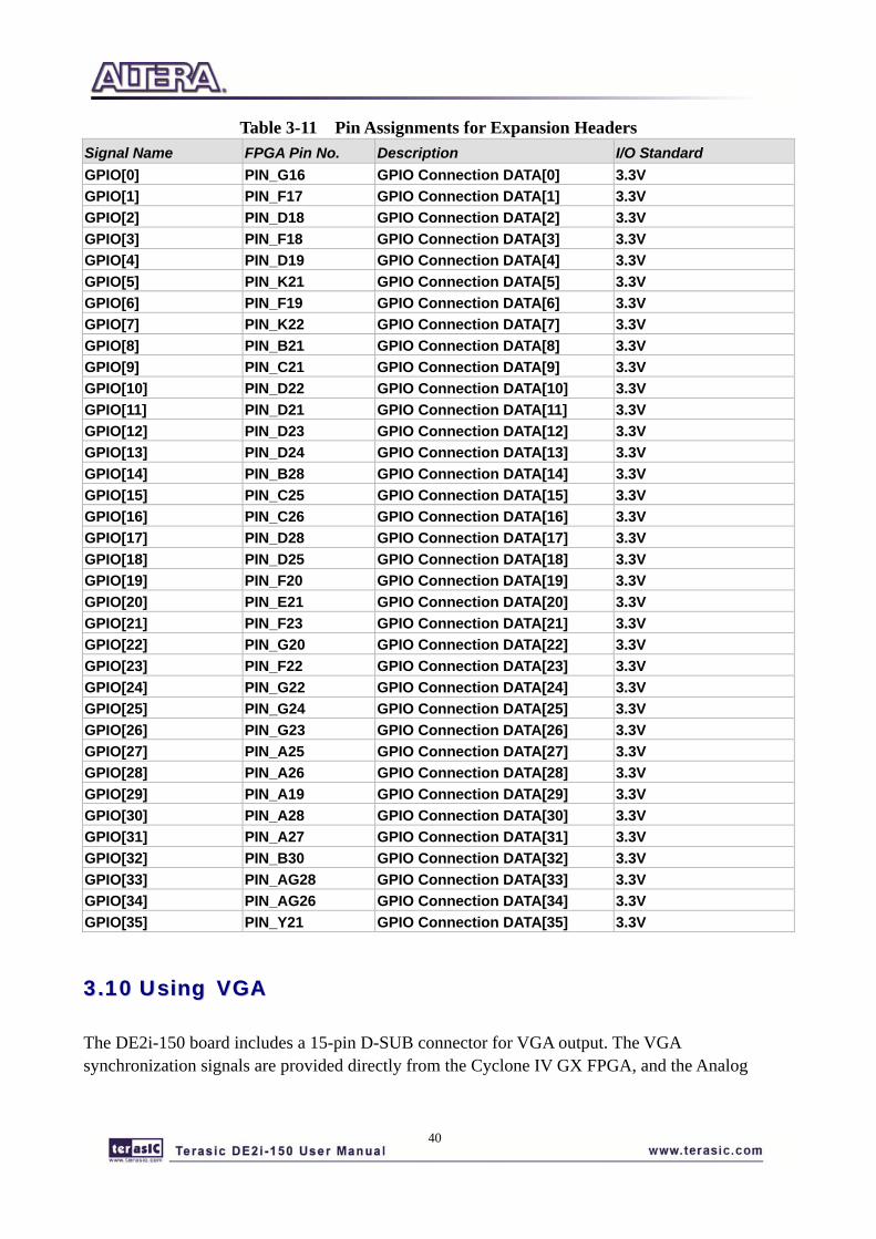
Table 3-11 Pin Assignments for Expansion Headers Signal Name FPGA Pin No. Description I/O Standard GPIO[0] PIN_G16 GPIO Connection DATA[0] 3.3V GPIO[1] PIN_F17 GPIO Connection DATA[1] 3.3V GPIO[2] PIN_D18 GPIO Connection DATA[2] 3.3V GPIO[3] PIN_F18 GPIO Connection DATA[3] 3.3V GPIO[4] PIN_D19 GPIO Connection DATA[4] 3.3V GPIO[5] PIN_K21 GPIO Connection DATA[5] 3.3V GPIO[6] PIN_F19 GPIO Connection DATA[6] 3.3V GPIO[7] PIN_K22 GPIO Connection DATA[7] 3.3V GPIO[8] PIN_B21 GPIO Connection DATA[8] 3.3V GPIO[9] PIN_C21 GPIO Connection DATA[9] 3.3V GPIO[10] PIN_D22 GPIO Connection DATA[10] 3.3V GPIO[11] PIN_D21 GPIO Connection DATA[11] 3.3V GPIO[12] PIN_D23 GPIO Connection DATA[12] 3.3V GPIO[13] PIN_D24 GPIO Connection DATA[13] 3.3V GPIO[14] PIN_B28 GPIO Connection DATA[14] 3.3V GPIO[15] PIN_C25 GPIO Connection DATA[15] 3.3V GPIO[16] PIN_C26 GPIO Connection DATA[16] 3.3V GPIO[17] PIN_D28 GPIO Connection DATA[17] 3.3V GPIO[18] PIN_D25 GPIO Connection DATA[18] 3.3V GPIO[19] PIN_F20 GPIO Connection DATA[19] 3.3V GPIO[20] PIN_E21 GPIO Connection DATA[20] 3.3V GPIO[21] PIN_F23 GPIO Connection DATA[21] 3.3V GPIO[22] PIN_G20 GPIO Connection DATA[22] 3.3V GPIO[23] PIN_F22 GPIO Connection DATA[23] 3.3V GPIO[24] PIN_G22 GPIO Connection DATA[24] 3.3V GPIO[25] PIN_G24 GPIO Connection DATA[25] 3.3V GPIO[26] PIN_G23 GPIO Connection DATA[26] 3.3V GPIO[27] PIN_A25 GPIO Connection DATA[27] 3.3V GPIO[28] PIN_A26 GPIO Connection DATA[28] 3.3V GPIO[29] PIN_A19 GPIO Connection DATA[29] 3.3V GPIO[30] PIN_A28 GPIO Connection DATA[30] 3.3V GPIO[31] PIN_A27 GPIO Connection DATA[31] 3.3V GPIO[32] PIN_B30 GPIO Connection DATA[32] 3.3V GPIO[33] PIN_AG28 GPIO Connection DATA[33] 3.3V GPIO[34] PIN_AG26 GPIO Connection DATA[34] 3.3V GPIO[35] PIN_Y21 GPIO Connection DATA[35] 3.3V
33..1100 UUssiinngg VVGGAA
The DE2i-150 board includes a 15-pin D-SUB connector for VGA output. The VGA synchronization signals are provided directly from the Cyclone IV GX FPGA, and the Analog
41
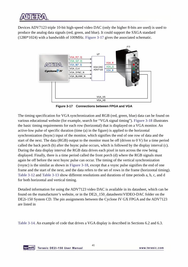
Devices ADV7123 triple 10-bit high-speed video DAC (only the higher 8-bits are used) is used to produce the analog data signals (red, green, and blue). It could support the SXGA standard (1280*1024) with a bandwidth of 100MHz. Figure 3-17 gives the associated schematic.
Figure 3-17 Connections between FPGA and VGA
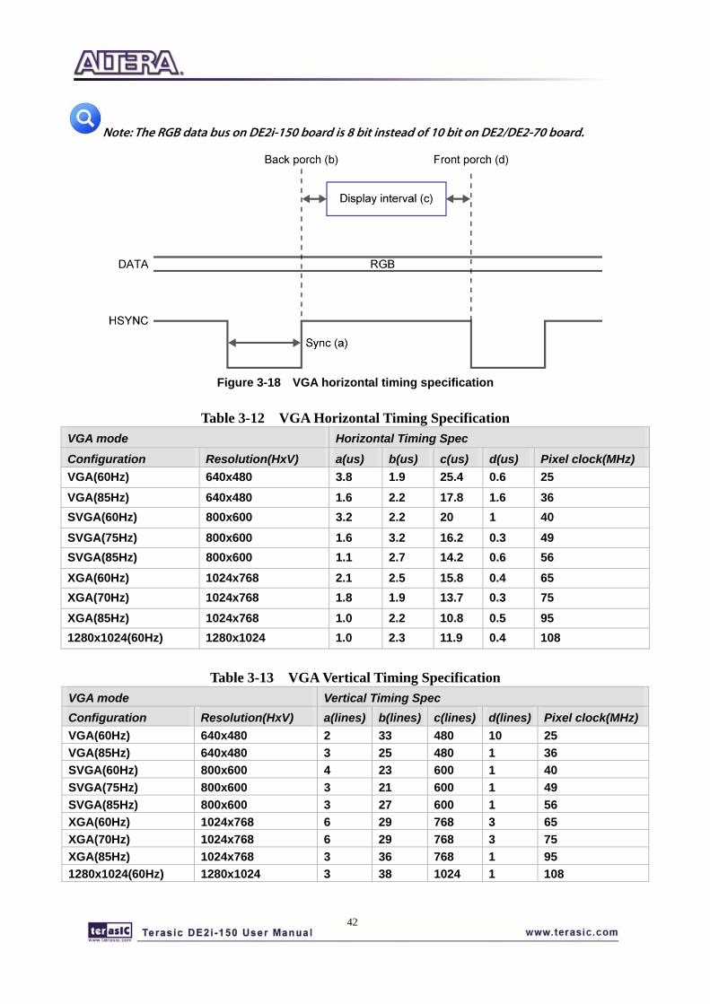
The timing specification for VGA synchronization and RGB (red, green, blue) data can be found on various educational website (for example, search for “VGA signal timing”). Figure 3-18 illustrates the basic timing requirements for each row (horizontal) that is displayed on a VGA monitor. An active-low pulse of specific duration (time (a) in the figure) is applied to the horizontal synchronization (hsync) input of the monitor, which signifies the end of one row of data and the start of the next. The data (RGB) output to the monitor must be off (driven to 0 V) for a time period called the back porch (b) after the hsync pulse occurs, which is followed by the display interval (c). During the data display interval the RGB data drives each pixel in turn across the row being displayed. Finally, there is a time period called the front porch (d) where the RGB signals must again be off before the next hsync pulse can occur. The timing of the vertical synchronization (vsync) is the similar as shown in Figure 3-18, except that a vsync pulse signifies the end of one frame and the start of the next, and the data refers to the set of rows in the frame (horizontal timing). Table 3-12 and Table 3-13 show different resolutions and durations of time periods a, b, c, and d for both horizontal and vertical timing.
Detailed information for using the ADV7123 video DAC is available in its datasheet, which can be found on the manufacturer’s website, or in the DE2i_150_datasheets\VIDEO-DAC folder on the DE2i-150 System CD. The pin assignments between the Cyclone IV GX FPGA and the ADV7123 are listed in
Table 3-14. An example of code that drives a VGA display is described in Sections 6.2 and 6.3.
42
Note: The RGB data bus on DE2i-150 board is 8 bit instead of 10 bit on DE2/DE2-70 board.
Figure 3-18 VGA horizontal timing specification
Table 3-12 VGA Horizontal Timing Specification VGA mode Horizontal Timing Spec Configuration Resolution(HxV) a(us) b(us) c(us) d(us) Pixel clock(MHz) VGA(60Hz) 640x480 3.8 1.9 25.4 0.6 25 VGA(85Hz) 640x480 1.6 2.2 17.8 1.6 36 SVGA(60Hz) 800x600 3.2 2.2 20 1 40 SVGA(75Hz) 800x600 1.6 3.2 16.2 0.3 49 SVGA(85Hz) 800x600 1.1 2.7 14.2 0.6 56 XGA(60Hz) 1024x768 2.1 2.5 15.8 0.4 65 XGA(70Hz) 1024x768 1.8 1.9 13.7 0.3 75 XGA(85Hz) 1024x768 1.0 2.2 10.8 0.5 95 1280x1024(60Hz) 1280x1024 1.0 2.3 11.9 0.4 108
Table 3-13 VGA Vertical Timing Specification
VGA mode Vertical Timing Spec Configuration Resolution(HxV) a(lines) b(lines) c(lines) d(lines) Pixel clock(MHz)VGA(60Hz) 640x480 2 33 480 10 25 VGA(85Hz) 640x480 3 25 480 1 36 SVGA(60Hz) 800x600 4 23 600 1 40 SVGA(75Hz) 800x600 3 21 600 1 49 SVGA(85Hz) 800x600 3 27 600 1 56 XGA(60Hz) 1024x768 6 29 768 3 65 XGA(70Hz) 1024x768 6 29 768 3 75 XGA(85Hz) 1024x768 3 36 768 1 95 1280x1024(60Hz) 1280x1024 3 38 1024 1 108
43
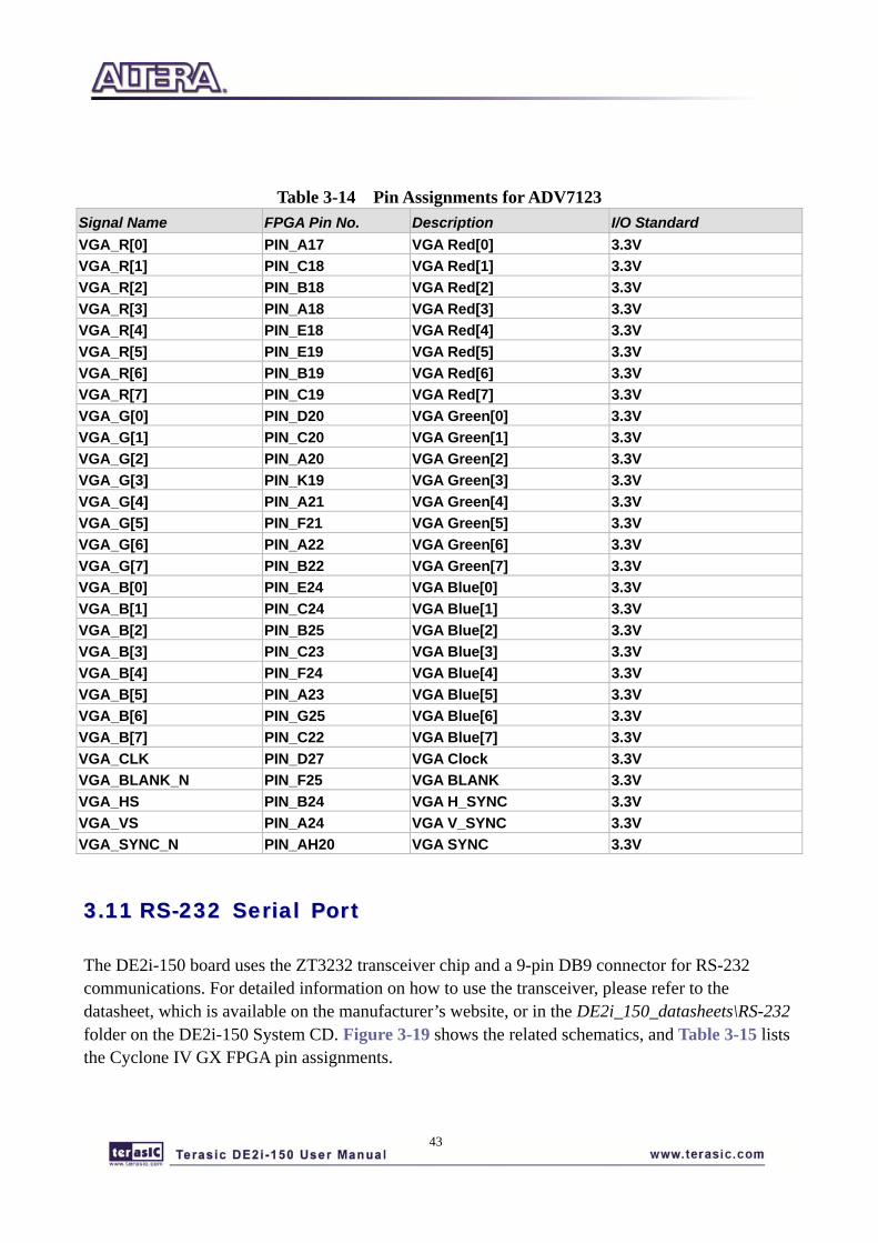
Table 3-14 Pin Assignments for ADV7123 Signal Name FPGA Pin No. Description I/O Standard VGA_R[0] PIN_A17 VGA Red[0] 3.3V VGA_R[1] PIN_C18 VGA Red[1] 3.3V VGA_R[2] PIN_B18 VGA Red[2] 3.3V VGA_R[3] PIN_A18 VGA Red[3] 3.3V VGA_R[4] PIN_E18 VGA Red[4] 3.3V VGA_R[5] PIN_E19 VGA Red[5] 3.3V VGA_R[6] PIN_B19 VGA Red[6] 3.3V VGA_R[7] PIN_C19 VGA Red[7] 3.3V VGA_G[0] PIN_D20 VGA Green[0] 3.3V VGA_G[1] PIN_C20 VGA Green[1] 3.3V VGA_G[2] PIN_A20 VGA Green[2] 3.3V VGA_G[3] PIN_K19 VGA Green[3] 3.3V VGA_G[4] PIN_A21 VGA Green[4] 3.3V VGA_G[5] PIN_F21 VGA Green[5] 3.3V VGA_G[6] PIN_A22 VGA Green[6] 3.3V VGA_G[7] PIN_B22 VGA Green[7] 3.3V VGA_B[0] PIN_E24 VGA Blue[0] 3.3V VGA_B[1] PIN_C24 VGA Blue[1] 3.3V VGA_B[2] PIN_B25 VGA Blue[2] 3.3V VGA_B[3] PIN_C23 VGA Blue[3] 3.3V VGA_B[4] PIN_F24 VGA Blue[4] 3.3V VGA_B[5] PIN_A23 VGA Blue[5] 3.3V VGA_B[6] PIN_G25 VGA Blue[6] 3.3V VGA_B[7] PIN_C22 VGA Blue[7] 3.3V VGA_CLK PIN_D27 VGA Clock 3.3V VGA_BLANK_N PIN_F25 VGA BLANK 3.3V VGA_HS PIN_B24 VGA H_SYNC 3.3V VGA_VS PIN_A24 VGA V_SYNC 3.3V VGA_SYNC_N PIN_AH20 VGA SYNC 3.3V
33..1111 RRSS--223322 SSeerriiaall PPoorrtt
The DE2i-150 board uses the ZT3232 transceiver chip and a 9-pin DB9 connector for RS-232 communications. For detailed information on how to use the transceiver, please refer to the datasheet, which is available on the manufacturer’s website, or in the DE2i_150_datasheets\RS-232 folder on the DE2i-150 System CD. Figure 3-19 shows the related schematics, and Table 3-15 lists the Cyclone IV GX FPGA pin assignments.
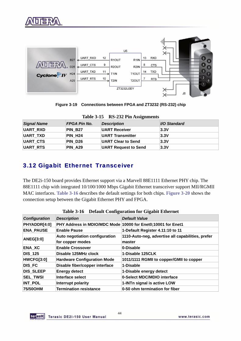
44
Figure 3-19 Connections between FPGA and ZT3232 (RS-232) chip
Table 3-15 RS-232 Pin Assignments Signal Name FPGA Pin No. Description I/O Standard UART_RXD PIN_B27 UART Receiver 3.3V UART_TXD PIN_H24 UART Transmitter 3.3V UART_CTS PIN_D26 UART Clear to Send 3.3V UART_RTS PIN_A29 UART Request to Send 3.3V
33..1122 GGiiggaabbiitt EEtthheerrnneett TTrraannsscceeiivveerr
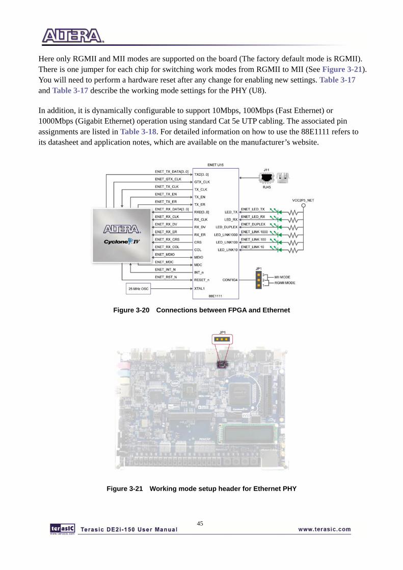
The DE2i-150 board provides Ethernet support via a Marvell 88E1111 Ethernet PHY chip. The 88E1111 chip with integrated 10/100/1000 Mbps Gigabit Ethernet transceiver support MII/RGMII MAC interfaces. Table 3-16 describes the default settings for both chips. Figure 3-20 shows the connection setup between the Gigabit Ethernet PHY and FPGA.
Table 3-16 Default Configuration for Gigabit Ethernet Configuration Description Default Value PHYADDR[4:0] PHY Address in MDIO/MDC Mode 10000 for Enet0;10001 for Enet1 ENA_PAUSE Enable Pause 1-Default Register 4.11:10 to 11
ANEG[3:0] Auto negotiation configuration for copper modes
1110-Auto-neg, advertise all capabilities, prefer master
ENA_XC Enable Crossover 0-Disable DIS_125 Disable 125MHz clock 1-Disable 125CLK HWCFG[3:0] Hardware Configuration Mode 1011/1111 RGMII to copper/GMII to copper DIS_FC Disable fiber/copper interface 1-Disable DIS_SLEEP Energy detect 1-Disable energy detect SEL_TWSI Interface select 0-Select MDC/MDIO interface INT_POL Interrupt polarity 1-INTn signal is active LOW 75/50OHM Termination resistance 0-50 ohm termination for fiber
45
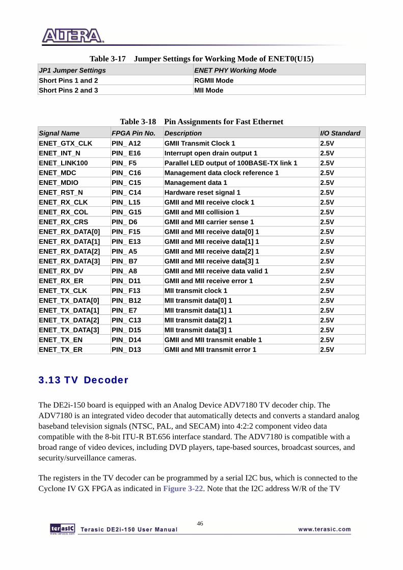
Here only RGMII and MII modes are supported on the board (The factory default mode is RGMII). There is one jumper for each chip for switching work modes from RGMII to MII (See Figure 3-21). You will need to perform a hardware reset after any change for enabling new settings. Table 3-17 and Table 3-17 describe the working mode settings for the PHY (U8).
In addition, it is dynamically configurable to support 10Mbps, 100Mbps (Fast Ethernet) or 1000Mbps (Gigabit Ethernet) operation using standard Cat 5e UTP cabling. The associated pin assignments are listed in Table 3-18. For detailed information on how to use the 88E1111 refers to its datasheet and application notes, which are available on the manufacturer’s website.
Figure 3-20 Connections between FPGA and Ethernet
Figure 3-21 Working mode setup header for Ethernet PHY
46
Table 3-17 Jumper Settings for Working Mode of ENET0(U15) JP1 Jumper Settings ENET PHY Working Mode Short Pins 1 and 2 RGMII Mode Short Pins 2 and 3 MII Mode
Table 3-18 Pin Assignments for Fast Ethernet Signal Name FPGA Pin No. Description I/O StandardENET_GTX_CLK PIN_ A12 GMII Transmit Clock 1 2.5V ENET_INT_N PIN_ E16 Interrupt open drain output 1 2.5V ENET_LINK100 PIN_ F5 Parallel LED output of 100BASE-TX link 1 2.5V ENET_MDC PIN_ C16 Management data clock reference 1 2.5V ENET_MDIO PIN_ C15 Management data 1 2.5V ENET_RST_N PIN_ C14 Hardware reset signal 1 2.5V ENET_RX_CLK PIN_ L15 GMII and MII receive clock 1 2.5V ENET_RX_COL PIN_ G15 GMII and MII collision 1 2.5V ENET_RX_CRS PIN_ D6 GMII and MII carrier sense 1 2.5V ENET_RX_DATA[0] PIN_ F15 GMII and MII receive data[0] 1 2.5V ENET_RX_DATA[1] PIN_ E13 GMII and MII receive data[1] 1 2.5V ENET_RX_DATA[2] PIN_ A5 GMII and MII receive data[2] 1 2.5V ENET_RX_DATA[3] PIN_ B7 GMII and MII receive data[3] 1 2.5V ENET_RX_DV PIN_ A8 GMII and MII receive data valid 1 2.5V ENET_RX_ER PIN_ D11 GMII and MII receive error 1 2.5V ENET_TX_CLK PIN_ F13 MII transmit clock 1 2.5V ENET_TX_DATA[0] PIN_ B12 MII transmit data[0] 1 2.5V ENET_TX_DATA[1] PIN_ E7 MII transmit data[1] 1 2.5V ENET_TX_DATA[2] PIN_ C13 MII transmit data[2] 1 2.5V ENET_TX_DATA[3] PIN_ D15 MII transmit data[3] 1 2.5V ENET_TX_EN PIN_ D14 GMII and MII transmit enable 1 2.5V ENET_TX_ER PIN_ D13 GMII and MII transmit error 1 2.5V
33..1133 TTVV DDeeccooddeerr
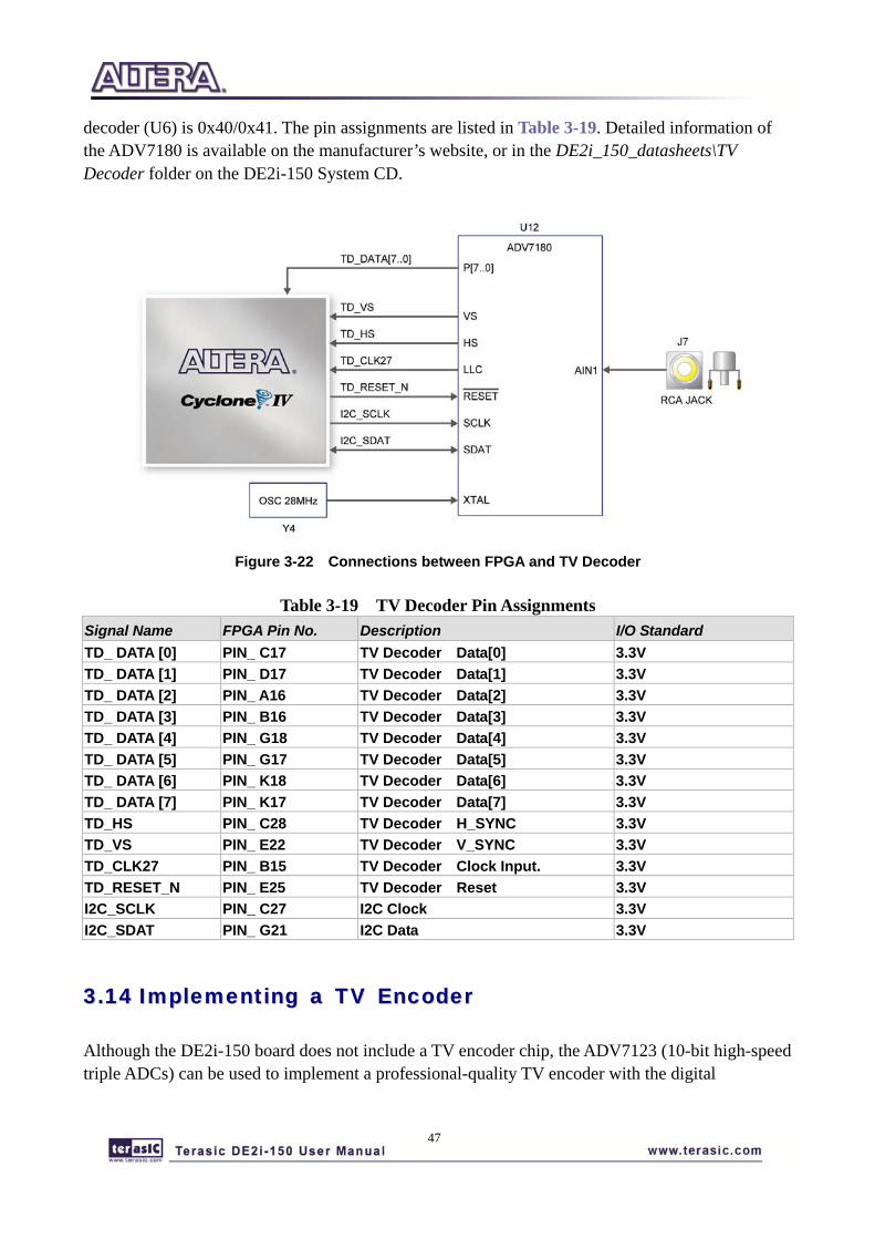
The DE2i-150 board is equipped with an Analog Device ADV7180 TV decoder chip. The ADV7180 is an integrated video decoder that automatically detects and converts a standard analog baseband television signals (NTSC, PAL, and SECAM) into 4:2:2 component video data compatible with the 8-bit ITU-R BT.656 interface standard. The ADV7180 is compatible with a broad range of video devices, including DVD players, tape-based sources, broadcast sources, and security/surveillance cameras.
The registers in the TV decoder can be programmed by a serial I2C bus, which is connected to the Cyclone IV GX FPGA as indicated in Figure 3-22. Note that the I2C address W/R of the TV
47
decoder (U6) is 0x40/0x41. The pin assignments are listed in Table 3-19. Detailed information of the ADV7180 is available on the manufacturer’s website, or in the DE2i_150_datasheets\TV Decoder folder on the DE2i-150 System CD.
Figure 3-22 Connections between FPGA and TV Decoder
Table 3-19 TV Decoder Pin Assignments Signal Name FPGA Pin No. Description I/O Standard TD_ DATA [0] PIN_ C17 TV Decoder Data[0] 3.3V TD_ DATA [1] PIN_ D17 TV Decoder Data[1] 3.3V TD_ DATA [2] PIN_ A16 TV Decoder Data[2] 3.3V TD_ DATA [3] PIN_ B16 TV Decoder Data[3] 3.3V TD_ DATA [4] PIN_ G18 TV Decoder Data[4] 3.3V TD_ DATA [5] PIN_ G17 TV Decoder Data[5] 3.3V TD_ DATA [6] PIN_ K18 TV Decoder Data[6] 3.3V TD_ DATA [7] PIN_ K17 TV Decoder Data[7] 3.3V TD_HS PIN_ C28 TV Decoder H_SYNC 3.3V TD_VS PIN_ E22 TV Decoder V_SYNC 3.3V TD_CLK27 PIN_ B15 TV Decoder Clock Input. 3.3V TD_RESET_N PIN_ E25 TV Decoder Reset 3.3V I2C_SCLK PIN_ C27 I2C Clock 3.3V I2C_SDAT PIN_ G21 I2C Data 3.3V
33..1144 IImmpplleemmeennttiinngg aa TTVV EEnnccooddeerr
Although the DE2i-150 board does not include a TV encoder chip, the ADV7123 (10-bit high-speed triple ADCs) can be used to implement a professional-quality TV encoder with the digital
48
processing part implemented in the Cyclone IV GX FPGA. Figure 3-23 shows a block diagram of a TV encoder implemented in this manner.
Figure 3-23 A TV Encoder that uses the Cyclone IV GX FPGA and the ADV7123
33..1155 UUssiinngg IIRR
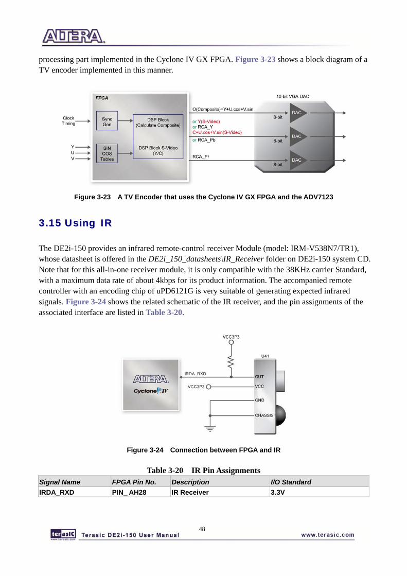
The DE2i-150 provides an infrared remote-control receiver Module (model: IRM-V538N7/TR1), whose datasheet is offered in the DE2i_150_datasheets\IR_Receiver folder on DE2i-150 system CD. Note that for this all-in-one receiver module, it is only compatible with the 38KHz carrier Standard, with a maximum data rate of about 4kbps for its product information. The accompanied remote controller with an encoding chip of uPD6121G is very suitable of generating expected infrared signals. Figure 3-24 shows the related schematic of the IR receiver, and the pin assignments of the associated interface are listed in Table 3-20.
Figure 3-24 Connection between FPGA and IR
Table 3-20 IR Pin Assignments Signal Name FPGA Pin No. Description I/O Standard IRDA_RXD PIN_ AH28 IR Receiver 3.3V
49
33..1166 UUssiinngg SSSSRRAAMM//SSDDRRAAMM//FFLLAASSHH//SSDD CCaarrdd
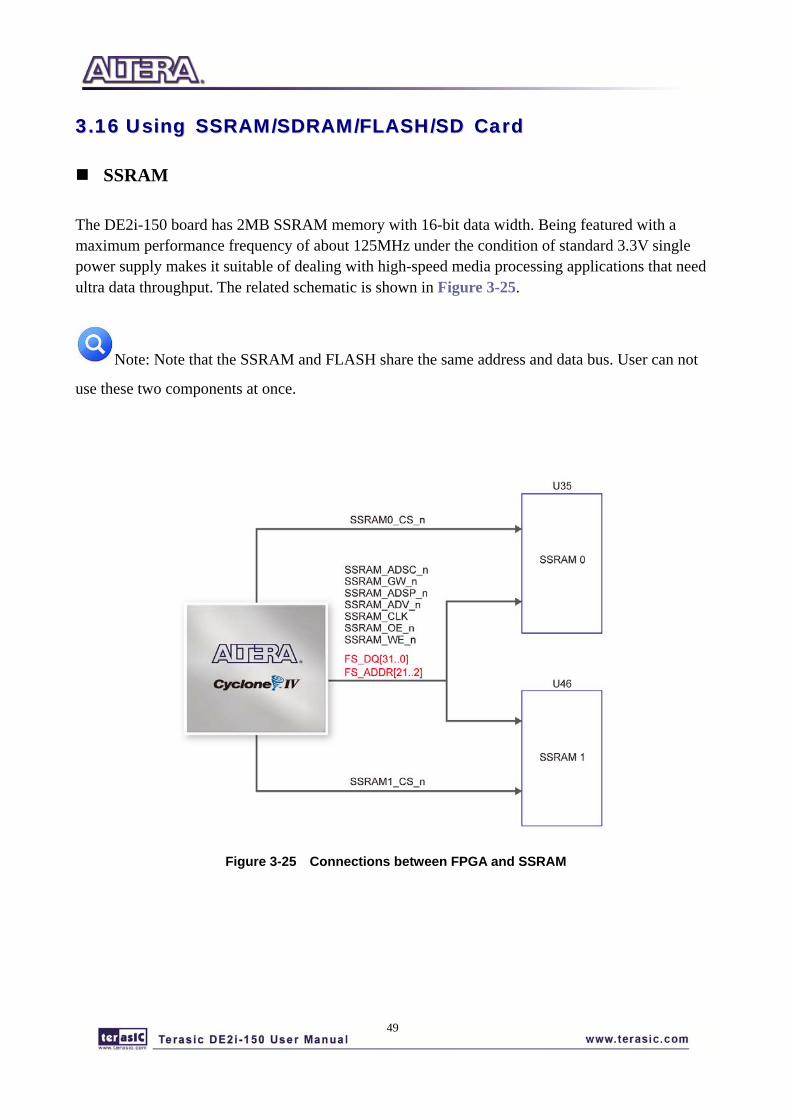
SSRAM
The DE2i-150 board has 2MB SSRAM memory with 16-bit data width. Being featured with a maximum performance frequency of about 125MHz under the condition of standard 3.3V single power supply makes it suitable of dealing with high-speed media processing applications that need ultra data throughput. The related schematic is shown in Figure 3-25.
Note: Note that the SSRAM and FLASH share the same address and data bus. User can not
use these two components at once.
Figure 3-25 Connections between FPGA and SSRAM
50
SDRAM
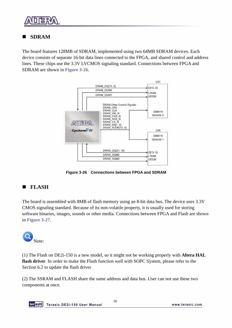
The board features 128MB of SDRAM, implemented using two 64MB SDRAM devices. Each device consists of separate 16-bit data lines connected to the FPGA, and shared control and address lines. These chips use the 3.3V LVCMOS signaling standard. Connections between FPGA and SDRAM are shown in Figure 3-26.
Figure 3-26 Connections between FPGA and SDRAM
FLASH
The board is assembled with 8MB of flash memory using an 8-bit data bus. The device uses 3.3V CMOS signaling standard. Because of its non-volatile property, it is usually used for storing software binaries, images, sounds or other media. Connections between FPGA and Flash are shown in Figure 3-27.
Note:
(1) The Flash on DE2i-150 is a new model, so it might not be working properly with Altera HAL flash driver. In order to make the Flash function well with SOPC System, please refer to the Section 6.2 to update the flash driver
(2) The SSRAM and FLASH share the same address and data bus. User can not use these two components at once.
51
Figure 3-27 Connections between FPGA and Flash
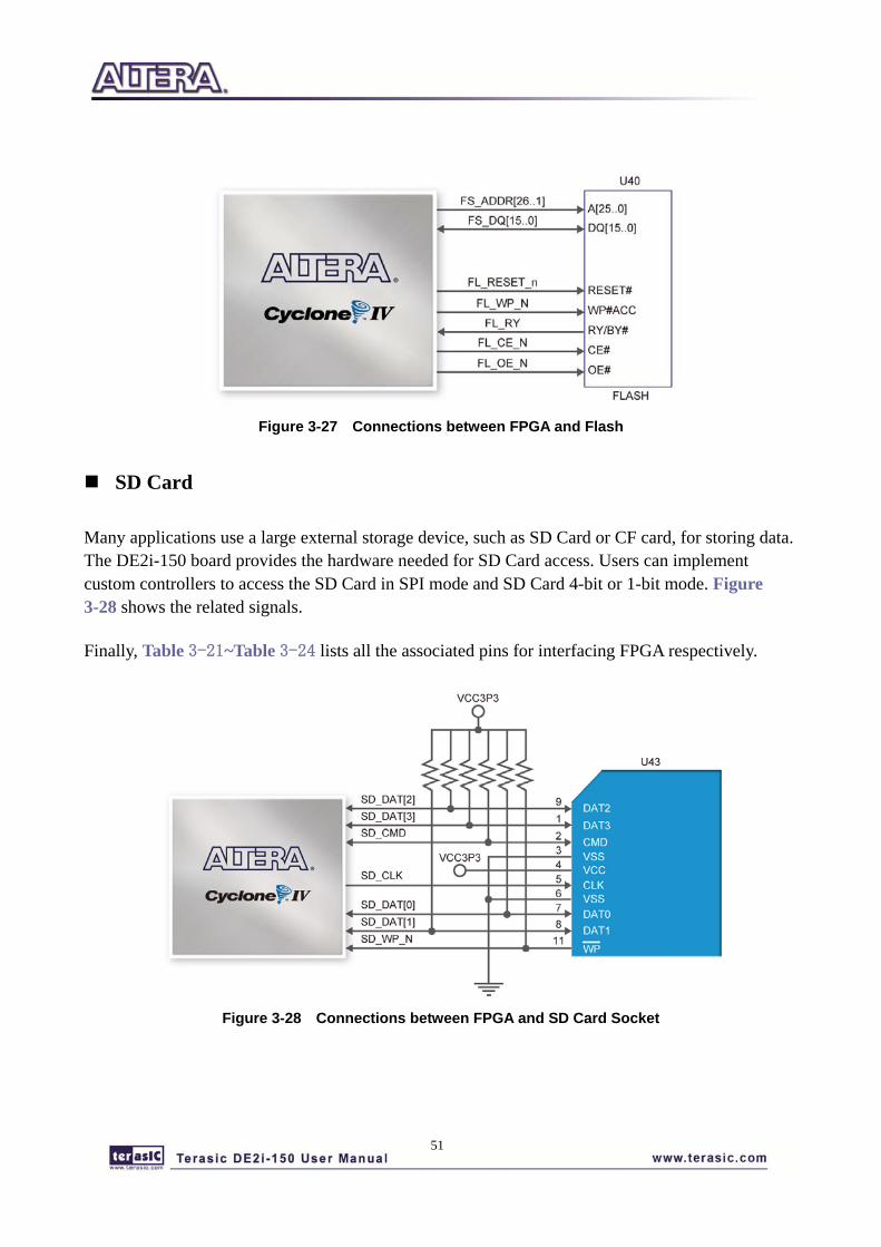
SD Card
Many applications use a large external storage device, such as SD Card or CF card, for storing data. The DE2i-150 board provides the hardware needed for SD Card access. Users can implement custom controllers to access the SD Card in SPI mode and SD Card 4-bit or 1-bit mode. Figure 3-28 shows the related signals.
Finally, Table 3-21~Table 3-24 lists all the associated pins for interfacing FPGA respectively.
Figure 3-28 Connections between FPGA and SD Card Socket
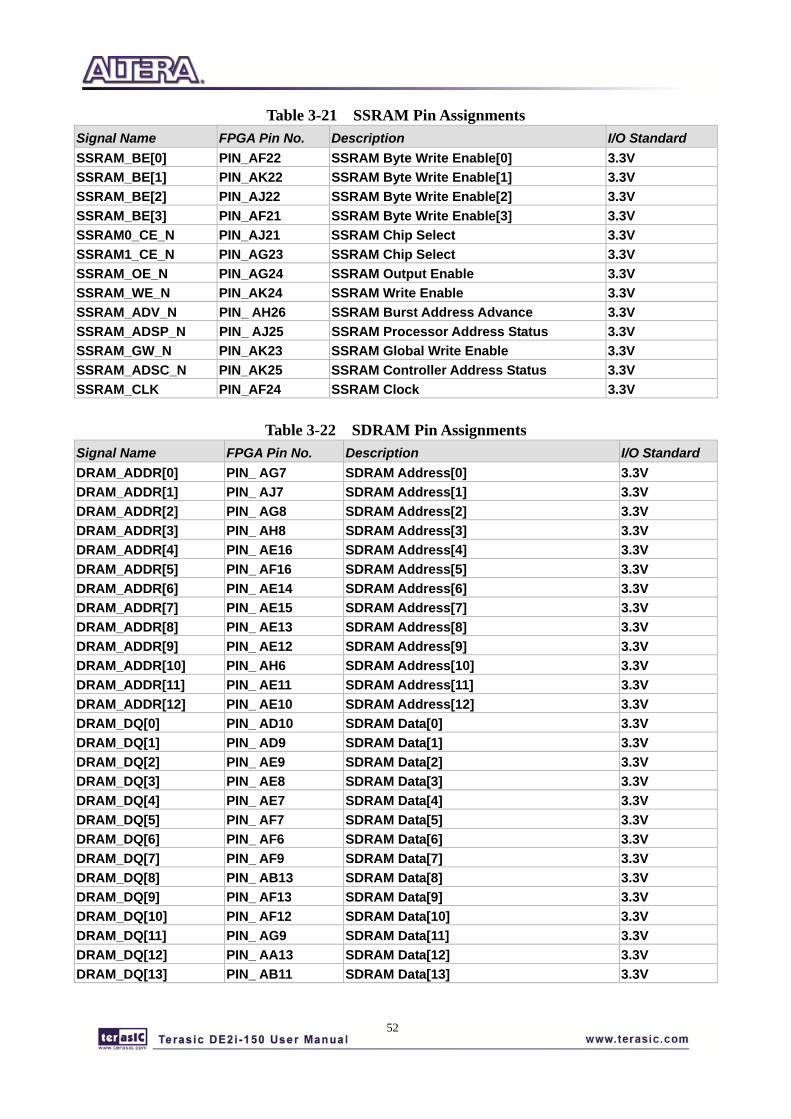
52
Table 3-21 SSRAM Pin Assignments Signal Name FPGA Pin No. Description I/O Standard SSRAM_BE[0] PIN_AF22 SSRAM Byte Write Enable[0] 3.3V SSRAM_BE[1] PIN_AK22 SSRAM Byte Write Enable[1] 3.3V SSRAM_BE[2] PIN_AJ22 SSRAM Byte Write Enable[2] 3.3V SSRAM_BE[3] PIN_AF21 SSRAM Byte Write Enable[3] 3.3V SSRAM0_CE_N PIN_AJ21 SSRAM Chip Select 3.3V SSRAM1_CE_N PIN_AG23 SSRAM Chip Select 3.3V SSRAM_OE_N PIN_AG24 SSRAM Output Enable 3.3V SSRAM_WE_N PIN_AK24 SSRAM Write Enable 3.3V SSRAM_ADV_N PIN_ AH26 SSRAM Burst Address Advance 3.3V SSRAM_ADSP_N PIN_ AJ25 SSRAM Processor Address Status 3.3V SSRAM_GW_N PIN_AK23 SSRAM Global Write Enable 3.3V SSRAM_ADSC_N PIN_AK25 SSRAM Controller Address Status 3.3V SSRAM_CLK PIN_AF24 SSRAM Clock 3.3V
Table 3-22 SDRAM Pin Assignments
Signal Name FPGA Pin No. Description I/O Standard DRAM_ADDR[0] PIN_ AG7 SDRAM Address[0] 3.3V DRAM_ADDR[1] PIN_ AJ7 SDRAM Address[1] 3.3V DRAM_ADDR[2] PIN_ AG8 SDRAM Address[2] 3.3V DRAM_ADDR[3] PIN_ AH8 SDRAM Address[3] 3.3V DRAM_ADDR[4] PIN_ AE16 SDRAM Address[4] 3.3V DRAM_ADDR[5] PIN_ AF16 SDRAM Address[5] 3.3V DRAM_ADDR[6] PIN_ AE14 SDRAM Address[6] 3.3V DRAM_ADDR[7] PIN_ AE15 SDRAM Address[7] 3.3V DRAM_ADDR[8] PIN_ AE13 SDRAM Address[8] 3.3V DRAM_ADDR[9] PIN_ AE12 SDRAM Address[9] 3.3V DRAM_ADDR[10] PIN_ AH6 SDRAM Address[10] 3.3V DRAM_ADDR[11] PIN_ AE11 SDRAM Address[11] 3.3V DRAM_ADDR[12] PIN_ AE10 SDRAM Address[12] 3.3V DRAM_DQ[0] PIN_ AD10 SDRAM Data[0] 3.3V DRAM_DQ[1] PIN_ AD9 SDRAM Data[1] 3.3V DRAM_DQ[2] PIN_ AE9 SDRAM Data[2] 3.3V DRAM_DQ[3] PIN_ AE8 SDRAM Data[3] 3.3V DRAM_DQ[4] PIN_ AE7 SDRAM Data[4] 3.3V DRAM_DQ[5] PIN_ AF7 SDRAM Data[5] 3.3V DRAM_DQ[6] PIN_ AF6 SDRAM Data[6] 3.3V DRAM_DQ[7] PIN_ AF9 SDRAM Data[7] 3.3V DRAM_DQ[8] PIN_ AB13 SDRAM Data[8] 3.3V DRAM_DQ[9] PIN_ AF13 SDRAM Data[9] 3.3V DRAM_DQ[10] PIN_ AF12 SDRAM Data[10] 3.3V DRAM_DQ[11] PIN_ AG9 SDRAM Data[11] 3.3V DRAM_DQ[12] PIN_ AA13 SDRAM Data[12] 3.3V DRAM_DQ[13] PIN_ AB11 SDRAM Data[13] 3.3V
53
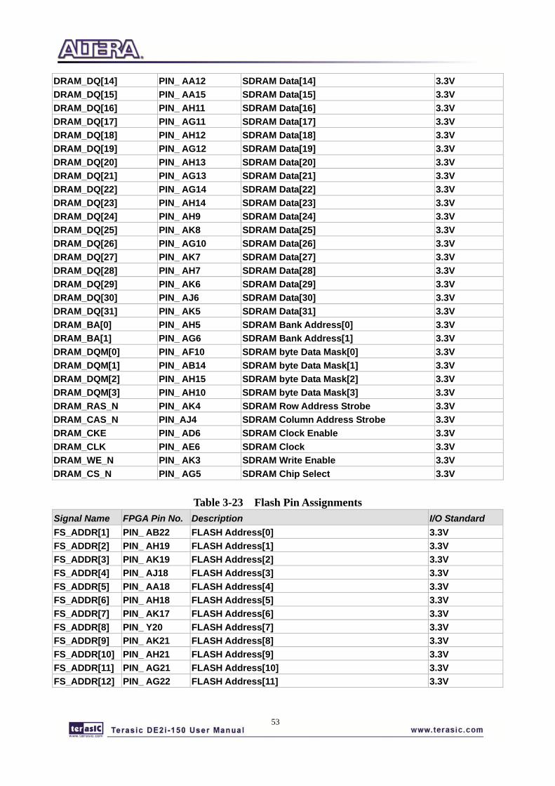
DRAM_DQ[14] PIN_ AA12 SDRAM Data[14] 3.3V DRAM_DQ[15] PIN_ AA15 SDRAM Data[15] 3.3V DRAM_DQ[16] PIN_ AH11 SDRAM Data[16] 3.3V DRAM_DQ[17] PIN_ AG11 SDRAM Data[17] 3.3V DRAM_DQ[18] PIN_ AH12 SDRAM Data[18] 3.3V DRAM_DQ[19] PIN_ AG12 SDRAM Data[19] 3.3V DRAM_DQ[20] PIN_ AH13 SDRAM Data[20] 3.3V DRAM_DQ[21] PIN_ AG13 SDRAM Data[21] 3.3V DRAM_DQ[22] PIN_ AG14 SDRAM Data[22] 3.3V DRAM_DQ[23] PIN_ AH14 SDRAM Data[23] 3.3V DRAM_DQ[24] PIN_ AH9 SDRAM Data[24] 3.3V DRAM_DQ[25] PIN_ AK8 SDRAM Data[25] 3.3V DRAM_DQ[26] PIN_ AG10 SDRAM Data[26] 3.3V DRAM_DQ[27] PIN_ AK7 SDRAM Data[27] 3.3V DRAM_DQ[28] PIN_ AH7 SDRAM Data[28] 3.3V DRAM_DQ[29] PIN_ AK6 SDRAM Data[29] 3.3V DRAM_DQ[30] PIN_ AJ6 SDRAM Data[30] 3.3V DRAM_DQ[31] PIN_ AK5 SDRAM Data[31] 3.3V DRAM_BA[0] PIN_ AH5 SDRAM Bank Address[0] 3.3V DRAM_BA[1] PIN_ AG6 SDRAM Bank Address[1] 3.3V DRAM_DQM[0] PIN_ AF10 SDRAM byte Data Mask[0] 3.3V DRAM_DQM[1] PIN_ AB14 SDRAM byte Data Mask[1] 3.3V DRAM_DQM[2] PIN_ AH15 SDRAM byte Data Mask[2] 3.3V DRAM_DQM[3] PIN_ AH10 SDRAM byte Data Mask[3] 3.3V DRAM_RAS_N PIN_ AK4 SDRAM Row Address Strobe 3.3V DRAM_CAS_N PIN_AJ4 SDRAM Column Address Strobe 3.3V DRAM_CKE PIN_ AD6 SDRAM Clock Enable 3.3V DRAM_CLK PIN_ AE6 SDRAM Clock 3.3V DRAM_WE_N PIN_ AK3 SDRAM Write Enable 3.3V DRAM_CS_N PIN_ AG5 SDRAM Chip Select 3.3V
Table 3-23 Flash Pin Assignments
Signal Name FPGA Pin No. Description I/O Standard FS_ADDR[1] PIN_ AB22 FLASH Address[0] 3.3V FS_ADDR[2] PIN_ AH19 FLASH Address[1] 3.3V FS_ADDR[3] PIN_ AK19 FLASH Address[2] 3.3V FS_ADDR[4] PIN_ AJ18 FLASH Address[3] 3.3V FS_ADDR[5] PIN_ AA18 FLASH Address[4] 3.3V FS_ADDR[6] PIN_ AH18 FLASH Address[5] 3.3V FS_ADDR[7] PIN_ AK17 FLASH Address[6] 3.3V FS_ADDR[8] PIN_ Y20 FLASH Address[7] 3.3V FS_ADDR[9] PIN_ AK21 FLASH Address[8] 3.3V FS_ADDR[10] PIN_ AH21 FLASH Address[9] 3.3V FS_ADDR[11] PIN_ AG21 FLASH Address[10] 3.3V FS_ADDR[12] PIN_ AG22 FLASH Address[11] 3.3V
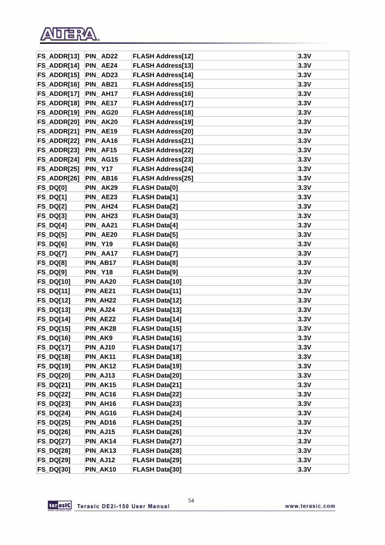
54
FS_ADDR[13] PIN_ AD22 FLASH Address[12] 3.3V FS_ADDR[14] PIN_ AE24 FLASH Address[13] 3.3V FS_ADDR[15] PIN_ AD23 FLASH Address[14] 3.3V FS_ADDR[16] PIN_ AB21 FLASH Address[15] 3.3V FS_ADDR[17] PIN_ AH17 FLASH Address[16] 3.3V FS_ADDR[18] PIN_ AE17 FLASH Address[17] 3.3V FS_ADDR[19] PIN_ AG20 FLASH Address[18] 3.3V FS_ADDR[20] PIN_ AK20 FLASH Address[19] 3.3V FS_ADDR[21] PIN_ AE19 FLASH Address[20] 3.3V FS_ADDR[22] PIN_ AA16 FLASH Address[21] 3.3V FS_ADDR[23] PIN_ AF15 FLASH Address[22] 3.3V FS_ADDR[24] PIN_ AG15 FLASH Address[23] 3.3V FS_ADDR[25] PIN_ Y17 FLASH Address[24] 3.3V FS_ADDR[26] PIN_ AB16 FLASH Address[25] 3.3V FS_DQ[0] PIN_ AK29 FLASH Data[0] 3.3V FS_DQ[1] PIN_ AE23 FLASH Data[1] 3.3V FS_DQ[2] PIN_ AH24 FLASH Data[2] 3.3V FS_DQ[3] PIN_ AH23 FLASH Data[3] 3.3V FS_DQ[4] PIN_ AA21 FLASH Data[4] 3.3V FS_DQ[5] PIN_ AE20 FLASH Data[5] 3.3V FS_DQ[6] PIN_ Y19 FLASH Data[6] 3.3V FS_DQ[7] PIN_ AA17 FLASH Data[7] 3.3V FS_DQ[8] PIN_AB17 FLASH Data[8] 3.3V FS_DQ[9] PIN_ Y18 FLASH Data[9] 3.3V FS_DQ[10] PIN_AA20 FLASH Data[10] 3.3V FS_DQ[11] PIN_AE21 FLASH Data[11] 3.3V FS_DQ[12] PIN_AH22 FLASH Data[12] 3.3V FS_DQ[13] PIN_AJ24 FLASH Data[13] 3.3V FS_DQ[14] PIN_AE22 FLASH Data[14] 3.3V FS_DQ[15] PIN_AK28 FLASH Data[15] 3.3V FS_DQ[16] PIN_AK9 FLASH Data[16] 3.3V FS_DQ[17] PIN_AJ10 FLASH Data[17] 3.3V FS_DQ[18] PIN_AK11 FLASH Data[18] 3.3V FS_DQ[19] PIN_AK12 FLASH Data[19] 3.3V FS_DQ[20] PIN_AJ13 FLASH Data[20] 3.3V FS_DQ[21] PIN_AK15 FLASH Data[21] 3.3V FS_DQ[22] PIN_AC16 FLASH Data[22] 3.3V FS_DQ[23] PIN_AH16 FLASH Data[23] 3.3V FS_DQ[24] PIN_AG16 FLASH Data[24] 3.3V FS_DQ[25] PIN_AD16 FLASH Data[25] 3.3V FS_DQ[26] PIN_AJ15 FLASH Data[26] 3.3V FS_DQ[27] PIN_AK14 FLASH Data[27] 3.3V FS_DQ[28] PIN_AK13 FLASH Data[28] 3.3V FS_DQ[29] PIN_AJ12 FLASH Data[29] 3.3V FS_DQ[30] PIN_AK10 FLASH Data[30] 3.3V
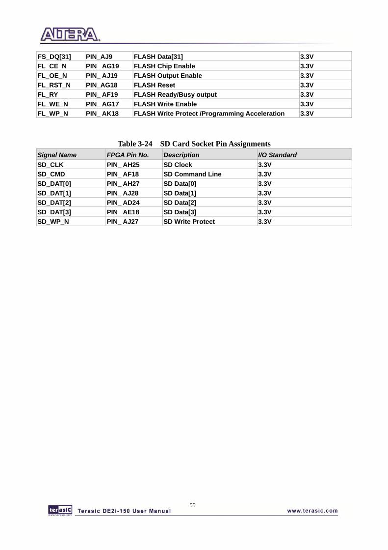
55
FS_DQ[31] PIN_AJ9 FLASH Data[31] 3.3V FL_CE_N PIN_ AG19 FLASH Chip Enable 3.3V FL_OE_N PIN_ AJ19 FLASH Output Enable 3.3V FL_RST_N PIN_AG18 FLASH Reset 3.3V FL_RY PIN_ AF19 FLASH Ready/Busy output 3.3V FL_WE_N PIN_ AG17 FLASH Write Enable 3.3V FL_WP_N PIN_ AK18 FLASH Write Protect /Programming Acceleration 3.3V
Table 3-24 SD Card Socket Pin Assignments Signal Name FPGA Pin No. Description I/O Standard SD_CLK PIN_ AH25 SD Clock 3.3V SD_CMD PIN_ AF18 SD Command Line 3.3V SD_DAT[0] PIN_ AH27 SD Data[0] 3.3V SD_DAT[1] PIN_ AJ28 SD Data[1] 3.3V SD_DAT[2] PIN_ AD24 SD Data[2] 3.3V SD_DAT[3] PIN_ AE18 SD Data[3] 3.3V SD_WP_N PIN_ AJ27 SD Write Protect 3.3V
56
Chapter 4 DE2i-150 System Builder
This chapter describes how users can create a custom design project on the DE2i-150 board by using DE2i-150 Software Tool – DE2i-150 System Builder.
44..11 IInnttrroodduuccttiioonn
The DE2i-150 System Builder is a Windows based software utility, designed to assist users to create a Quartus II project for the DE2i-150 board within minutes. The generated Quartus II project files include:
• Quartus II Project File (.qpf) • Quartus II Setting File (.qsf) • Top-Level Design File (.v) • Synopsis Design Constraints file (.sdc) • Pin Assignment Document (.htm)
By providing the above files, DE2i-150 System Builder prevents occurrence of situations that are prone to errors when users manually edit the top-level design file or place pin assignments. The common mistakes that users encounter are the following:
1. Board damaged due to wrong pin/bank voltage assignments.
2. Board malfunction caused by wrong device connections or missing pin counts for connected ends.
3. Performance degeneration because of improper pin assignments.
44..22 GGeenneerraall DDeessiiggnn FFllooww
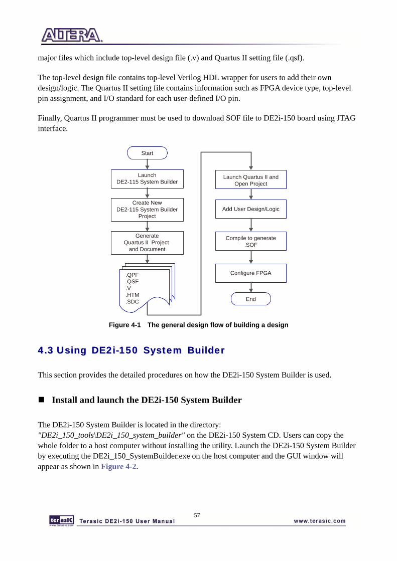
This section will introduce the general design flow to build a project for the DE2i-150 board via the DE2i-150 System Builder. The general design flow is illustrated in Figure 4-1.
Users should launch DE2i-150 System Builder and create a new project according to their design requirements. When users complete the settings, the DE2i-150 System Builder will generate two
57
major files which include top-level design file (.v) and Quartus II setting file (.qsf).
The top-level design file contains top-level Verilog HDL wrapper for users to add their own design/logic. The Quartus II setting file contains information such as FPGA device type, top-level pin assignment, and I/O standard for each user-defined I/O pin.
Finally, Quartus II programmer must be used to download SOF file to DE2i-150 board using JTAG interface.
Start
Launch Quartus II andOpen Project
Add User Design/Logic
Compile to generate.SOF
Configure FPGA
End
.QPF
.QSF
.V
.HTM
.SDC
LaunchDE2-115 System Builder
Create NewDE2-115 System Builder
Project
GenerateQuartus II Project
and Document
Figure 4-1 The general design flow of building a design
44..33 UUssiinngg DDEE22ii--115500 SSyysstteemm BBuuiillddeerr
This section provides the detailed procedures on how the DE2i-150 System Builder is used.
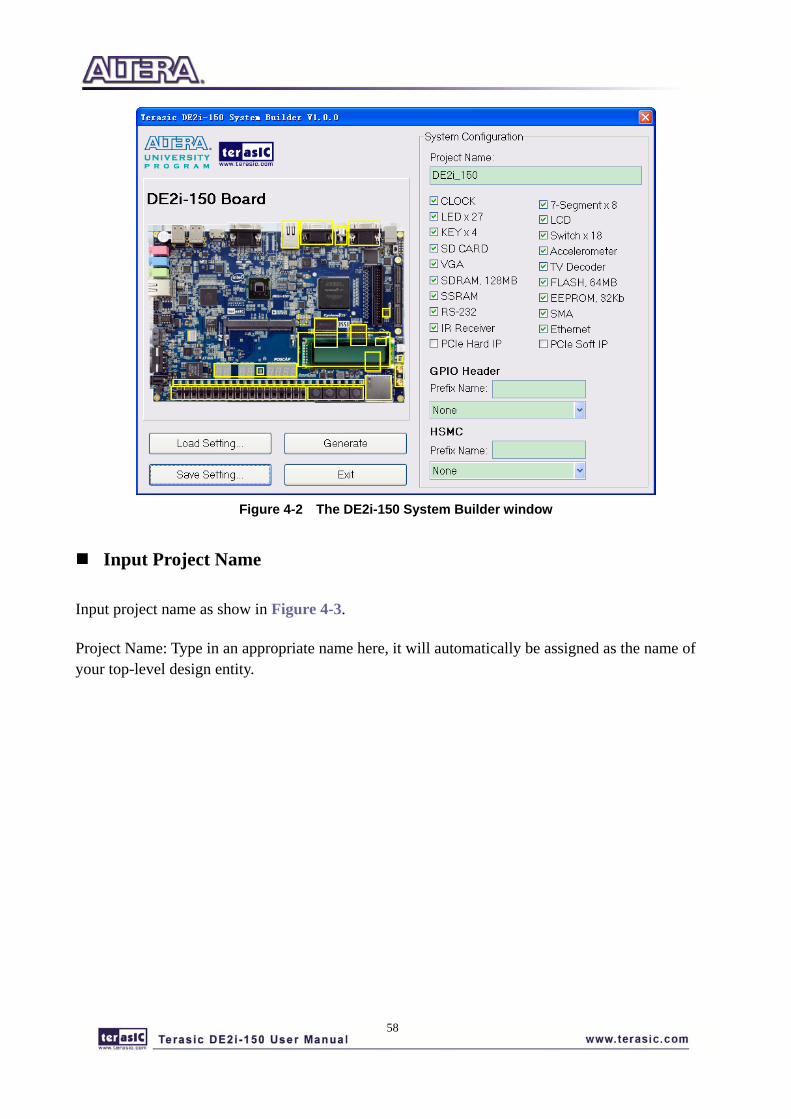
Install and launch the DE2i-150 System Builder
The DE2i-150 System Builder is located in the directory: "DE2i_150_tools\DE2i_150_system_builder" on the DE2i-150 System CD. Users can copy the whole folder to a host computer without installing the utility. Launch the DE2i-150 System Builder by executing the DE2i_150_SystemBuilder.exe on the host computer and the GUI window will appear as shown in Figure 4-2.
58
Figure 4-2 The DE2i-150 System Builder window
Input Project Name
Input project name as show in Figure 4-3.
Project Name: Type in an appropriate name here, it will automatically be assigned as the name of your top-level design entity.
59
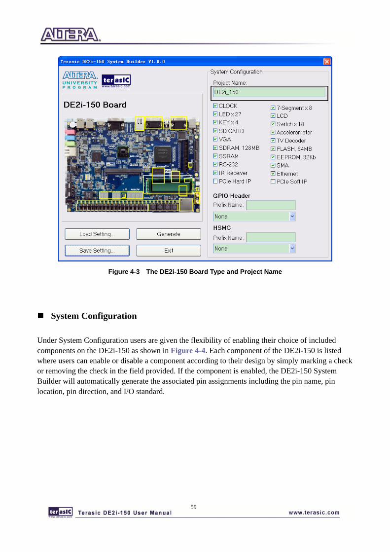
Figure 4-3 The DE2i-150 Board Type and Project Name
System Configuration
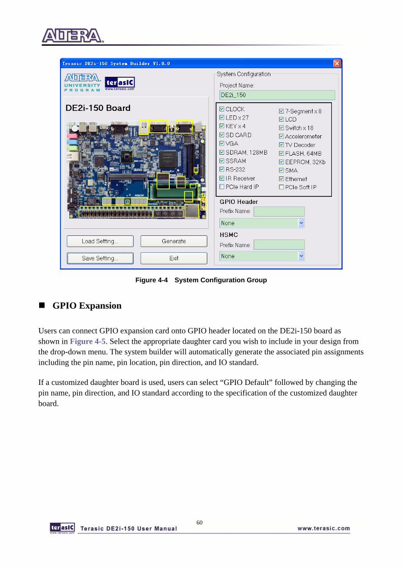
Under System Configuration users are given the flexibility of enabling their choice of included components on the DE2i-150 as shown in Figure 4-4. Each component of the DE2i-150 is listed where users can enable or disable a component according to their design by simply marking a check or removing the check in the field provided. If the component is enabled, the DE2i-150 System Builder will automatically generate the associated pin assignments including the pin name, pin location, pin direction, and I/O standard.
60
Figure 4-4 System Configuration Group
GPIO Expansion
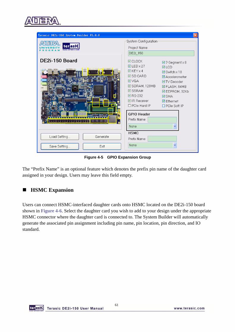
Users can connect GPIO expansion card onto GPIO header located on the DE2i-150 board as shown in Figure 4-5. Select the appropriate daughter card you wish to include in your design from the drop-down menu. The system builder will automatically generate the associated pin assignments including the pin name, pin location, pin direction, and IO standard.
If a customized daughter board is used, users can select “GPIO Default” followed by changing the pin name, pin direction, and IO standard according to the specification of the customized daughter board.
61
Figure 4-5 GPIO Expansion Group
The “Prefix Name” is an optional feature which denotes the prefix pin name of the daughter card assigned in your design. Users may leave this field empty.
HSMC Expansion
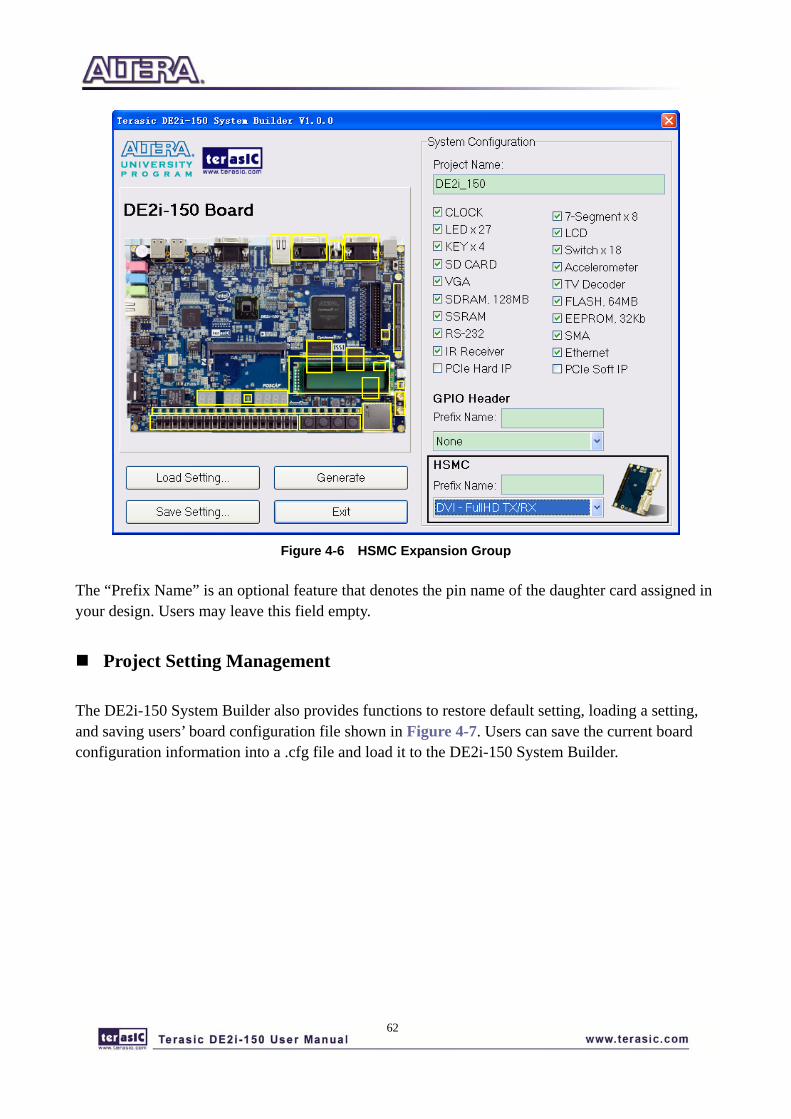
Users can connect HSMC-interfaced daughter cards onto HSMC located on the DE2i-150 board shown in Figure 4-6. Select the daughter card you wish to add to your design under the appropriate HSMC connector where the daughter card is connected to. The System Builder will automatically generate the associated pin assignment including pin name, pin location, pin direction, and IO standard.
62
Figure 4-6 HSMC Expansion Group
The “Prefix Name” is an optional feature that denotes the pin name of the daughter card assigned in your design. Users may leave this field empty.
Project Setting Management
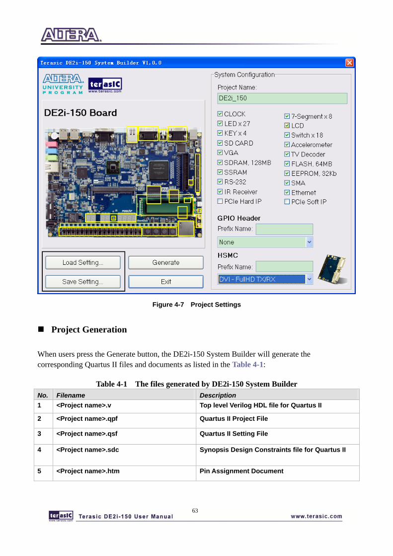
The DE2i-150 System Builder also provides functions to restore default setting, loading a setting, and saving users’ board configuration file shown in Figure 4-7. Users can save the current board configuration information into a .cfg file and load it to the DE2i-150 System Builder.
63
Figure 4-7 Project Settings
Project Generation
When users press the Generate button, the DE2i-150 System Builder will generate the corresponding Quartus II files and documents as listed in the Table 4-1:
Table 4-1 The files generated by DE2i-150 System Builder No. Filename Description 1 <Project name>.v Top level Verilog HDL file for Quartus II
2 <Project name>.qpf Quartus II Project File
3 <Project name>.qsf Quartus II Setting File
4 <Project name>.sdc Synopsis Design Constraints file for Quartus II
5 <Project name>.htm Pin Assignment Document
64
Users can use Quartus II software to add custom logic into the project and compile the project to generate the SSRAM Object File (.sof).
65
Chapter 5 Examples of Advanced Demonstrations
This chapter provides a number of examples of advanced circuits implemented on the DE2i-150 board. These circuits provide demonstrations of the major features on the board, such as its audio and video capabilities, USB, and Ethernet connectivity. For each demonstration the Cyclone IV GX FPGA (or EPCS64 serial EEPROM) configuration file is provided, as well as the full source code in Verilog HDL. All of the associated files can be found in the DE2i_150_demonstrations folder on the DE2i-150 System CD. For each demonstrations described in the following sections, the name of the project directory for its files is given, which are subdirectories of the DE2i_150_demonstrations folder.
Installing the Demonstrations
To install the demonstrations on your computer:
Copy the directory DE2i_150_demonstrations into a local directory of your choice. It is important to ensure that the path to your local directory contains no spaces – otherwise, the Nios II software will not work. Note: Version Quartus II v9.1 SP2 or later is required for all DE2i-150 demonstrations to support Cyclone IV GX device. Quartus II can be installed from the Altera Complete Design Suite DVD provided.
55..11 DDEE22ii--115500 FFaaccttoorryy CCoonnffiigguurraattiioonn
The DE2i-150 board is shipped from the factory with a default configuration bit-stream that demonstrates some of the basic features of the board. The setup required for this demonstration, and the locations of its files are shown below.
Demonstration Setup, File Locations, and Instructions
• Project directory: DE2i_150_Default • Bit stream used: DE2i_150_Default.sof or DE2i_150_Default.pof • Power on the DE2i-150 board, with the USB cable connected to the USB Blaster port. If
66
necessary (that is, if the default factory configuration of the DE2i-150 board is not currently stored in EPCS64 device), download the bit stream to the board by using either JTAG or AS programming
• You should now be able to observe that the 7-segment displays are displaying a sequence of characters, and the red and green LEDs are flashing. Also, “Welcome to the Altera DE2i-150” is shown on the LCD display
• Optionally connect a VGA display to the VGA D-SUB connector. When connected, the VGA display should show a color picture
• Optionally connect a powered speaker to the stereo audio-out jack • Place slide switch SW17 in the DOWN position to hear a 1 kHz humming sound from the
audio-out port. Alternatively, if slide switch SW17 is in the UP position, and optionally connects the microphone in port with a microphone and/or connects the line-in port with an audio player's output, you will hear the sound from the microphone or audio player or mixed sound from both.
The Verilog HDL source code for this demonstration is provided in the DE2i_150_Default folder, which also includes the necessary files for the corresponding Quartus II project. The top-level Verilog HDL file, called DE2i_150_Default.v, can be used as a template for other projects, because it defines ports that correspond to all of the user-accessible pins on the Cyclone IV GX FPGA.
55..22 TTVV BBooxx DDeemmoonnssttrraattiioonn
This demonstration plays video and audio input from a DVD player using the VGA output, audio CODEC, and one TV decoder (U6) on the DE2i-150 board. Figure 5-1 shows the block diagram of the design. There are two major blocks in the circuit, called I2C_AV_Config and TV_to_VGA. The TV_to_VGA block consists of the ITU-R 656 Decoder, SDRAM Frame Buffer, YUV422 to YUV444, YcrCb to RGB, and VGA Controller. The figure also shows the TV Decoder (ADV7180) and the VGA DAC (ADV7123) chips used.
As soon as the bit stream is downloaded into the FPGA, the register values of the TV Decoder chip are used to configure the TV decoder via the I2C_AV_Config block, which uses the I2C protocol to communicate with the TV Decoder chip. Following the power-on sequence, the TV Decoder chip will be unstable for a time period; the Lock Detector is responsible for detecting this instability.
The ITU-R 656 Decoder block extracts YcrCb 4:2:2 (YUV 4:2:2) video signals from the ITU-R 656 data stream sent from the TV Decoder. It also generates a data valid control signal indicating the valid period of data output. Because the video signal from the TV Decoder is interlaced, we need to perform de-interlacing on the data source. We used the SDRAM Frame Buffer and a field selection multiplexer (MUX) which is controlled by the VGA controller to perform the de-interlacing operation. Internally, the VGA Controller generates data request and odd/even selection signals to the SDRAM Frame Buffer and filed selection multiplexer (MUX). The YUV422 to YUV444 block converts the selected YcrCb 4:2:2 (YUV 4:2:2) video data to the YcrCb 4:4:4 (YUV 4:4:4) video data format.
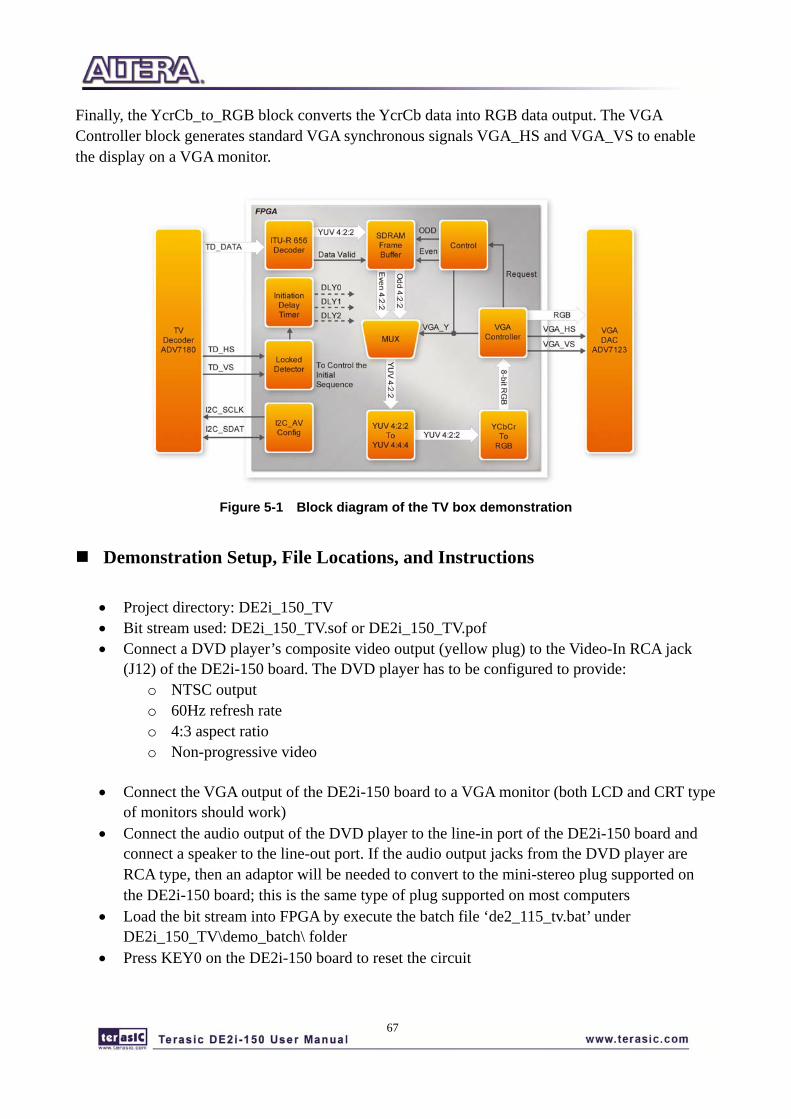
67
Finally, the YcrCb_to_RGB block converts the YcrCb data into RGB data output. The VGA Controller block generates standard VGA synchronous signals VGA_HS and VGA_VS to enable the display on a VGA monitor.
Figure 5-1 Block diagram of the TV box demonstration
Demonstration Setup, File Locations, and Instructions
• Project directory: DE2i_150_TV • Bit stream used: DE2i_150_TV.sof or DE2i_150_TV.pof • Connect a DVD player’s composite video output (yellow plug) to the Video-In RCA jack
(J12) of the DE2i-150 board. The DVD player has to be configured to provide: o NTSC output o 60Hz refresh rate o 4:3 aspect ratio o Non-progressive video
• Connect the VGA output of the DE2i-150 board to a VGA monitor (both LCD and CRT type of monitors should work)
• Connect the audio output of the DVD player to the line-in port of the DE2i-150 board and connect a speaker to the line-out port. If the audio output jacks from the DVD player are RCA type, then an adaptor will be needed to convert to the mini-stereo plug supported on the DE2i-150 board; this is the same type of plug supported on most computers
• Load the bit stream into FPGA by execute the batch file ‘de2_115_tv.bat’ under DE2i_150_TV\demo_batch\ folder
• Press KEY0 on the DE2i-150 board to reset the circuit
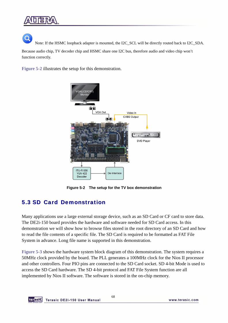
68
Note: If the HSMC loopback adapter is mounted, the I2C_SCL will be directly routed back to I2C_SDA.
Because audio chip, TV decoder chip and HSMC share one I2C bus, therefore audio and video chip won’t function correctly.
Figure 5-2 illustrates the setup for this demonstration.
Figure 5-2 The setup for the TV box demonstration
55..33 SSDD CCaarrdd DDeemmoonnssttrraattiioonn
Many applications use a large external storage device, such as an SD Card or CF card to store data. The DE2i-150 board provides the hardware and software needed for SD Card access. In this demonstration we will show how to browse files stored in the root directory of an SD Card and how to read the file contents of a specific file. The SD Card is required to be formatted as FAT File System in advance. Long file name is supported in this demonstration.
Figure 5-3 shows the hardware system block diagram of this demonstration. The system requires a 50MHz clock provided by the board. The PLL generates a 100MHz clock for the Nios II processor and other controllers. Four PIO pins are connected to the SD Card socket. SD 4-bit Mode is used to access the SD Card hardware. The SD 4-bit protocol and FAT File System function are all implemented by Nios II software. The software is stored in the on-chip memory.
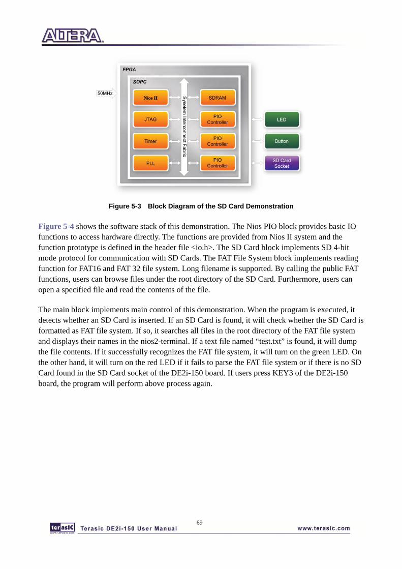
69
Figure 5-3 Block Diagram of the SD Card Demonstration
Figure 5-4 shows the software stack of this demonstration. The Nios PIO block provides basic IO functions to access hardware directly. The functions are provided from Nios II system and the function prototype is defined in the header file <io.h>. The SD Card block implements SD 4-bit mode protocol for communication with SD Cards. The FAT File System block implements reading function for FAT16 and FAT 32 file system. Long filename is supported. By calling the public FAT functions, users can browse files under the root directory of the SD Card. Furthermore, users can open a specified file and read the contents of the file.
The main block implements main control of this demonstration. When the program is executed, it detects whether an SD Card is inserted. If an SD Card is found, it will check whether the SD Card is formatted as FAT file system. If so, it searches all files in the root directory of the FAT file system and displays their names in the nios2-terminal. If a text file named “test.txt” is found, it will dump the file contents. If it successfully recognizes the FAT file system, it will turn on the green LED. On the other hand, it will turn on the red LED if it fails to parse the FAT file system or if there is no SD Card found in the SD Card socket of the DE2i-150 board. If users press KEY3 of the DE2i-150 board, the program will perform above process again.
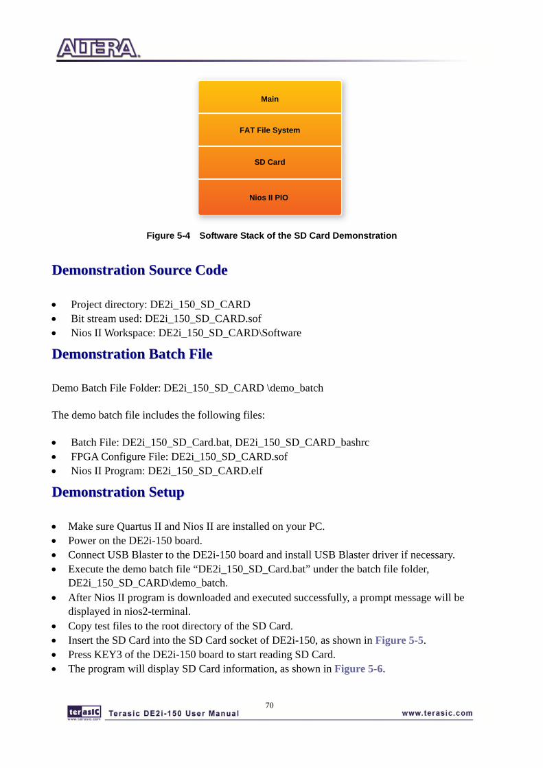
70
Main
FAT File System
SD Card
Nios II PIO
Figure 5-4 Software Stack of the SD Card Demonstration
DDeemmoonnssttrraattiioonn SSoouurrccee CCooddee
• Project directory: DE2i_150_SD_CARD • Bit stream used: DE2i_150_SD_CARD.sof • Nios II Workspace: DE2i_150_SD_CARD\Software
DDeemmoonnssttrraattiioonn BBaattcchh FFiillee
Demo Batch File Folder: DE2i_150_SD_CARD \demo_batch
The demo batch file includes the following files:
• Batch File: DE2i_150_SD_Card.bat, DE2i_150_SD_CARD_bashrc • FPGA Configure File: DE2i_150_SD_CARD.sof • Nios II Program: DE2i_150_SD_CARD.elf
DDeemmoonnssttrraattiioonn SSeettuupp
• Make sure Quartus II and Nios II are installed on your PC. • Power on the DE2i-150 board. • Connect USB Blaster to the DE2i-150 board and install USB Blaster driver if necessary. • Execute the demo batch file “DE2i_150_SD_Card.bat” under the batch file folder,
DE2i_150_SD_CARD\demo_batch. • After Nios II program is downloaded and executed successfully, a prompt message will be
displayed in nios2-terminal. • Copy test files to the root directory of the SD Card. • Insert the SD Card into the SD Card socket of DE2i-150, as shown in Figure 5-5. • Press KEY3 of the DE2i-150 board to start reading SD Card. • The program will display SD Card information, as shown in Figure 5-6.
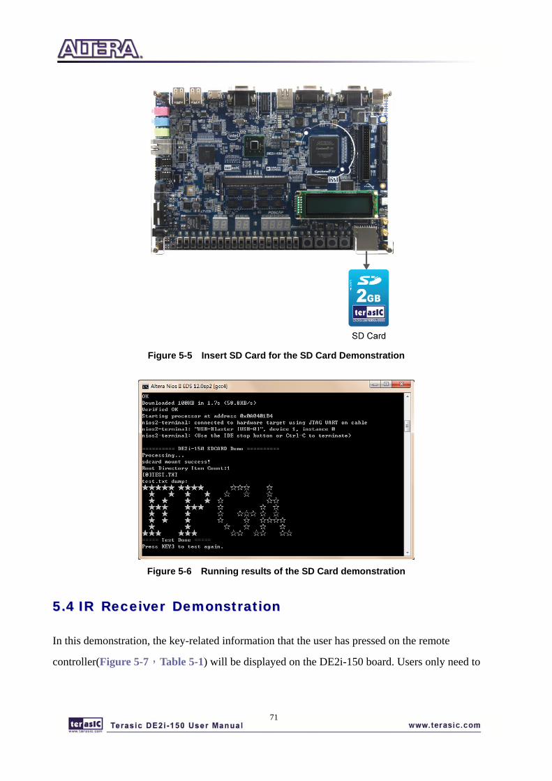
71
Figure 5-5 Insert SD Card for the SD Card Demonstration
Figure 5-6 Running results of the SD Card demonstration
55..44 IIRR RReecceeiivveerr DDeemmoonnssttrraattiioonn
In this demonstration, the key-related information that the user has pressed on the remote
controller(Figure 5-7,Table 5-1) will be displayed on the DE2i-150 board. Users only need to
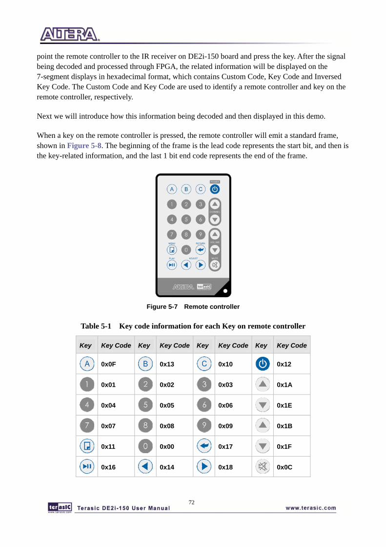
72
point the remote controller to the IR receiver on DE2i-150 board and press the key. After the signal being decoded and processed through FPGA, the related information will be displayed on the 7-segment displays in hexadecimal format, which contains Custom Code, Key Code and Inversed Key Code. The Custom Code and Key Code are used to identify a remote controller and key on the remote controller, respectively.
Next we will introduce how this information being decoded and then displayed in this demo.
When a key on the remote controller is pressed, the remote controller will emit a standard frame, shown in Figure 5-8. The beginning of the frame is the lead code represents the start bit, and then is the key-related information, and the last 1 bit end code represents the end of the frame.
Figure 5-7 Remote controller
Table 5-1 Key code information for each Key on remote controller
Key Key Code Key Key Code Key Key Code Key Key Code
0x0F
0x13 0x10 0x12
0x01
0x02 0x03 0x1A
0x04
0x05 0x06 0x1E
0x07
0x08 0x09 0x1B
0x11
0x00 0x17 0x1F
0x16
0x14 0x18 0x0C
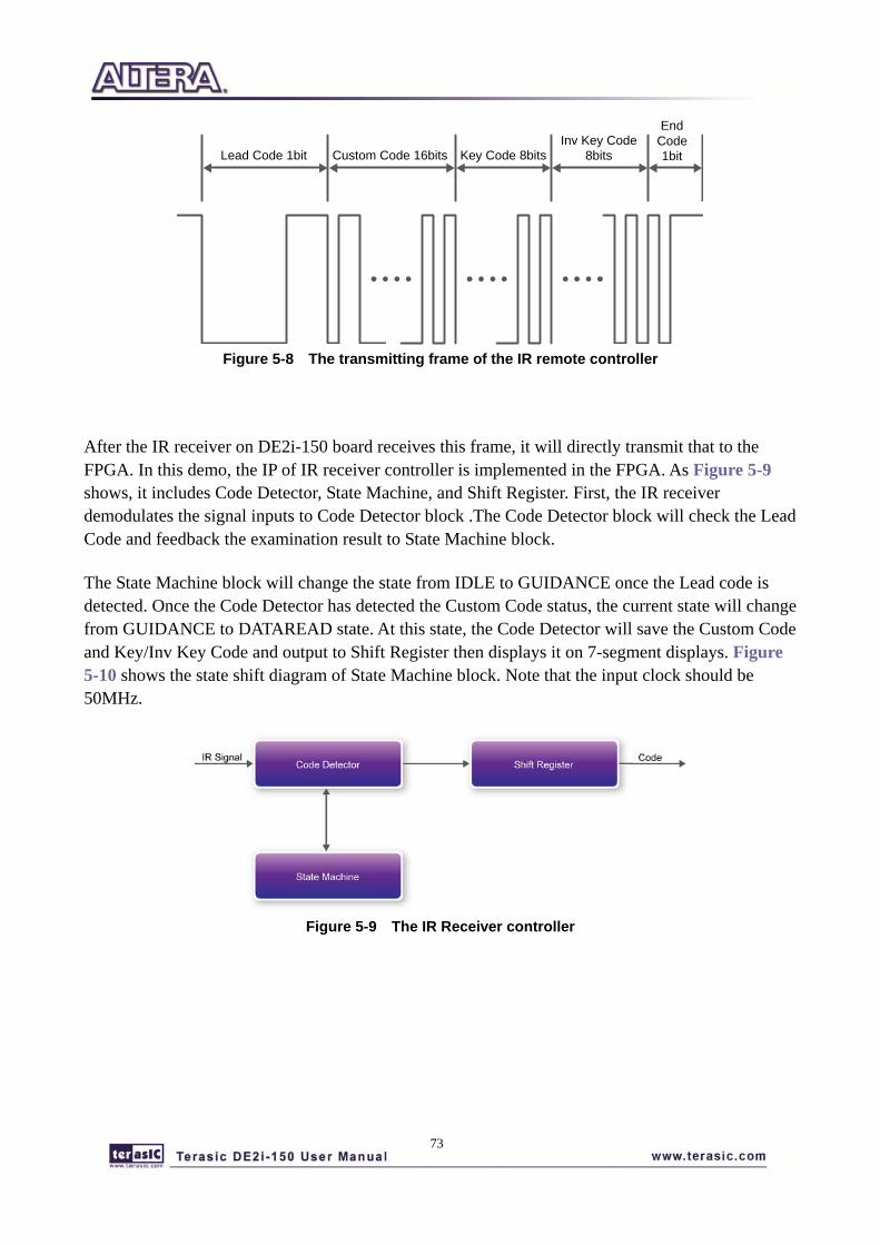
73
Lead Code 1bit Custom Code 16bits Key Code 8bitsInv Key Code
8bits
EndCode1bit
Figure 5-8 The transmitting frame of the IR remote controller
After the IR receiver on DE2i-150 board receives this frame, it will directly transmit that to the FPGA. In this demo, the IP of IR receiver controller is implemented in the FPGA. As Figure 5-9 shows, it includes Code Detector, State Machine, and Shift Register. First, the IR receiver demodulates the signal inputs to Code Detector block .The Code Detector block will check the Lead Code and feedback the examination result to State Machine block.
The State Machine block will change the state from IDLE to GUIDANCE once the Lead code is detected. Once the Code Detector has detected the Custom Code status, the current state will change from GUIDANCE to DATAREAD state. At this state, the Code Detector will save the Custom Code and Key/Inv Key Code and output to Shift Register then displays it on 7-segment displays. Figure 5-10 shows the state shift diagram of State Machine block. Note that the input clock should be 50MHz.
Figure 5-9 The IR Receiver controller
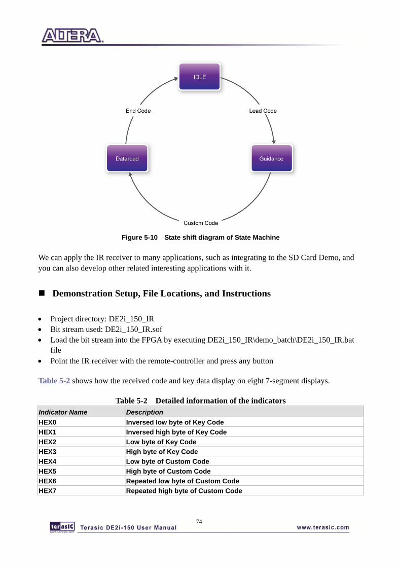
74
Figure 5-10 State shift diagram of State Machine
We can apply the IR receiver to many applications, such as integrating to the SD Card Demo, and you can also develop other related interesting applications with it.
Demonstration Setup, File Locations, and Instructions
• Project directory: DE2i_150_IR • Bit stream used: DE2i_150_IR.sof • Load the bit stream into the FPGA by executing DE2i_150_IR\demo_batch\DE2i_150_IR.bat
file • Point the IR receiver with the remote-controller and press any button
Table 5-2 shows how the received code and key data display on eight 7-segment displays.
Table 5-2 Detailed information of the indicators Indicator Name Description HEX0 Inversed low byte of Key Code HEX1 Inversed high byte of Key Code HEX2 Low byte of Key Code HEX3 High byte of Key Code HEX4 Low byte of Custom Code HEX5 High byte of Custom Code HEX6 Repeated low byte of Custom Code HEX7 Repeated high byte of Custom Code
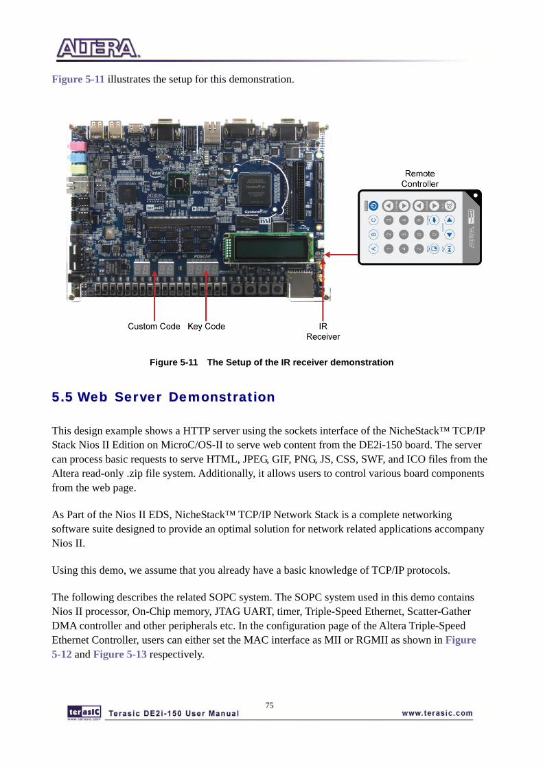
75
Figure 5-11 illustrates the setup for this demonstration.
Figure 5-11 The Setup of the IR receiver demonstration
55..55 WWeebb SSeerrvveerr DDeemmoonnssttrraattiioonn
This design example shows a HTTP server using the sockets interface of the NicheStack™ TCP/IP Stack Nios II Edition on MicroC/OS-II to serve web content from the DE2i-150 board. The server can process basic requests to serve HTML, JPEG, GIF, PNG, JS, CSS, SWF, and ICO files from the Altera read-only .zip file system. Additionally, it allows users to control various board components from the web page.
As Part of the Nios II EDS, NicheStack™ TCP/IP Network Stack is a complete networking software suite designed to provide an optimal solution for network related applications accompany Nios II.
Using this demo, we assume that you already have a basic knowledge of TCP/IP protocols.
The following describes the related SOPC system. The SOPC system used in this demo contains Nios II processor, On-Chip memory, JTAG UART, timer, Triple-Speed Ethernet, Scatter-Gather DMA controller and other peripherals etc. In the configuration page of the Altera Triple-Speed Ethernet Controller, users can either set the MAC interface as MII or RGMII as shown in Figure 5-12 and Figure 5-13 respectively.
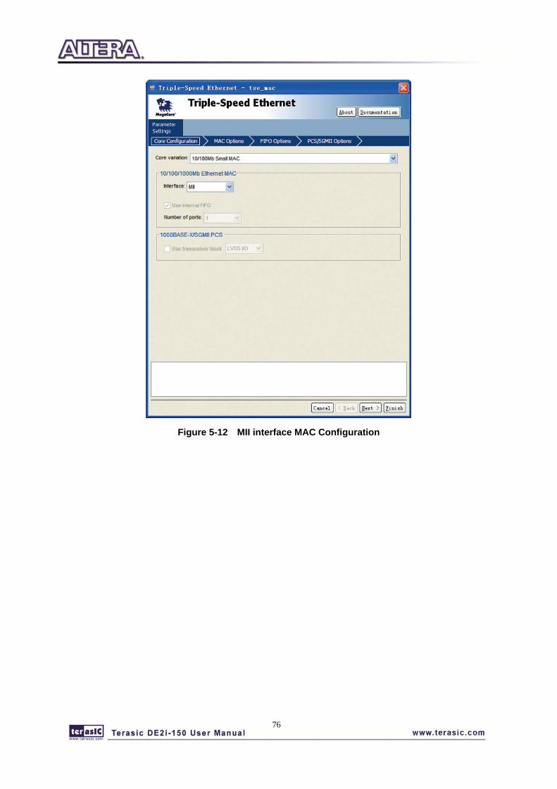
76
Figure 5-12 MII interface MAC Configuration
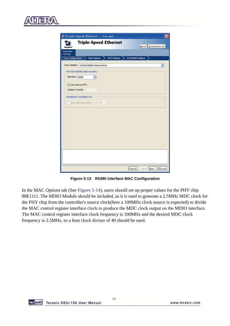
77
Figure 5-13 RGMII interface MAC Configuration
In the MAC Options tab (See Figure 5-14), users should set up proper values for the PHY chip 88E1111. The MDIO Module should be included, as it is used to generate a 2.5MHz MDC clock for the PHY chip from the controller's source clock(here a 100MHz clock source is expected) to divide the MAC control register interface clock to produce the MDC clock output on the MDIO interface. The MAC control register interface clock frequency is 100MHz and the desired MDC clock frequency is 2.5MHz, so a host clock divisor of 40 should be used.
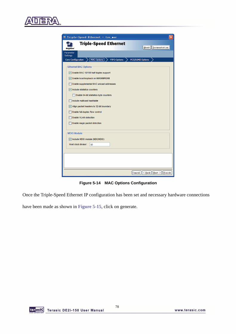
78
Figure 5-14 MAC Options Configuration
Once the Triple-Speed Ethernet IP configuration has been set and necessary hardware connections
have been made as shown in Figure 5-15, click on generate.
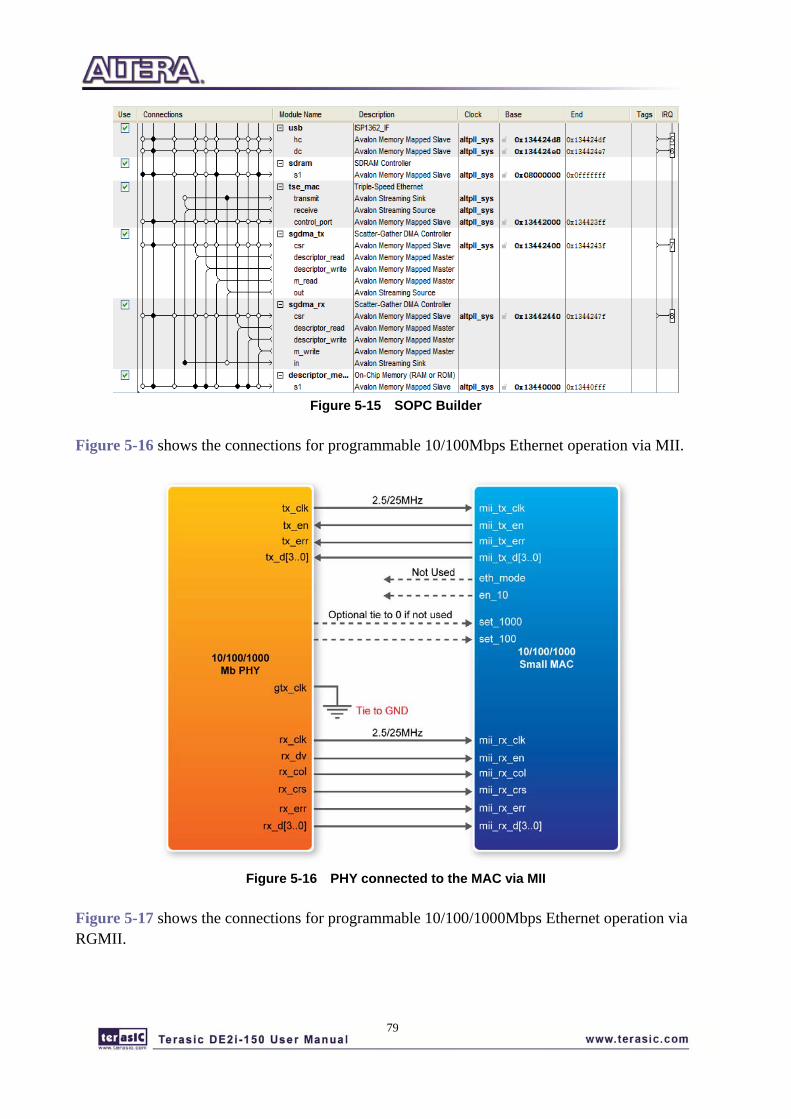
79
Figure 5-15 SOPC Builder
Figure 5-16 shows the connections for programmable 10/100Mbps Ethernet operation via MII.
Figure 5-16 PHY connected to the MAC via MII
Figure 5-17 shows the connections for programmable 10/100/1000Mbps Ethernet operation via RGMII.
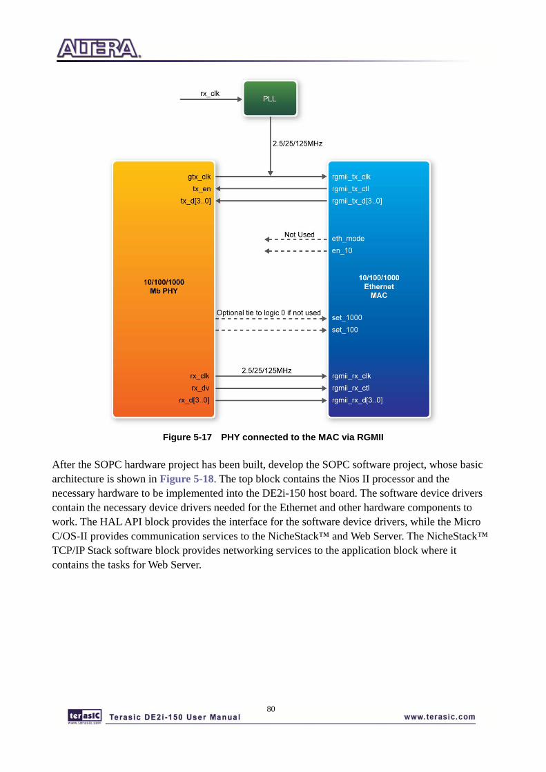
80
Figure 5-17 PHY connected to the MAC via RGMII
After the SOPC hardware project has been built, develop the SOPC software project, whose basic architecture is shown in Figure 5-18. The top block contains the Nios II processor and the necessary hardware to be implemented into the DE2i-150 host board. The software device drivers contain the necessary device drivers needed for the Ethernet and other hardware components to work. The HAL API block provides the interface for the software device drivers, while the Micro C/OS-II provides communication services to the NicheStack™ and Web Server. The NicheStack™ TCP/IP Stack software block provides networking services to the application block where it contains the tasks for Web Server.
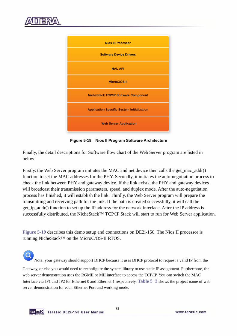
81
Nios II Processor
Software Device Drivers
HAL API
MicroC/OS-II
NicheStack TCP/IP Software Component
Application Specific System Initialization
Web Server Application
Figure 5-18 Nios II Program Software Architecture
Finally, the detail descriptions for Software flow chart of the Web Server program are listed in below:
Firstly, the Web Server program initiates the MAC and net device then calls the get_mac_addr() function to set the MAC addresses for the PHY. Secondly, it initiates the auto-negotiation process to check the link between PHY and gateway device. If the link exists, the PHY and gateway devices will broadcast their transmission parameters, speed, and duplex mode. After the auto-negotiation process has finished, it will establish the link. Thirdly, the Web Server program will prepare the transmitting and receiving path for the link. If the path is created successfully, it will call the get_ip_addr() function to set up the IP address for the network interface. After the IP address is successfully distributed, the NicheStack™ TCP/IP Stack will start to run for Web Server application.
Figure 5-19 describes this demo setup and connections on DE2i-150. The Nios II processor is running NicheStack™ on the MicroC/OS-II RTOS.
Note: your gateway should support DHCP because it uses DHCP protocol to request a valid IP from the
Gateway, or else you would need to reconfigure the system library to use static IP assignment. Furthermore, the web server demonstration uses the RGMII or MII interface to access the TCP/IP. You can switch the MAC Interface via JP1 and JP2 for Ethernet 0 and Ethernet 1 respectively. Table 5-3 shows the project name of web server demonstration for each Ethernet Port and working mode.
82
Table 5-3 Demo Directory Paths
PHY project directory Interface
ENET0 ENET1
RGMII interface
DE2i_150_Web_Server\ DE2i_150_WEB_SERVER_RGMII_ENET0
DE2i_150_Web_Server\ DE2i_150_WEB_SERVER_RGMII_ENET1
MII interface
DE2i_150_Web_Server\ DE2i_150_WEB_SERVER_MII_ENET0
DE2i_150_Web_Server\ DE2i_150_WEB_SERVER_MII_ENET1
Demonstration Setup, File Locations, and Instructions
The Following steps describe how to setup a Web Server demonstration on the ENET0 in RGMII mode.
• Project directory: DE2i_150_Web_Server\ DE2i_150_WEB_SERVER_RGMII_ENET0 • Nios II Project workspace: Project directory\software • Bit stream used: DE2i_150_WEB_SERVER.sof • Web site content zip file: ro_zipfs.zip • Make sure the PHY device is working on RGMII mode (Short pin 1 and pin 2 of JP1) • Launch Quartus II and download the web server demo bit stream into FPGA • Launch Nios II IDE and open the Nios II Project workspace • Download the web site content zip file into FLASH memory using the Flash Programmer in
Nios II IDE • Plug a CAT 5e cable into the Ethernet port (J4) on the DE2i-150 board • Select ‘Run->Run as Nios II Hardware’ in Nios II IDE window to run this project (note *) • Once the LCD on DE2i-150 board shows the valid IP address got from Gateway, then launch
your web browser • Input the IP into your browser. (IP is shown on the LCD display) • You will see the brand new DE2i-150 webpage on your computer • On the web page, you could access the DE2i-150 board’s peripherals from the left sidebar or
link to external pages from the right sidebar. Try check some LEDs on the left sidebar and then press send will light up the specified LEDs on board. You also could send text to the LCD or set the value for 7-segment displays on DE2i-150 board. Figure 5-20 gives a snapshot of the web server page
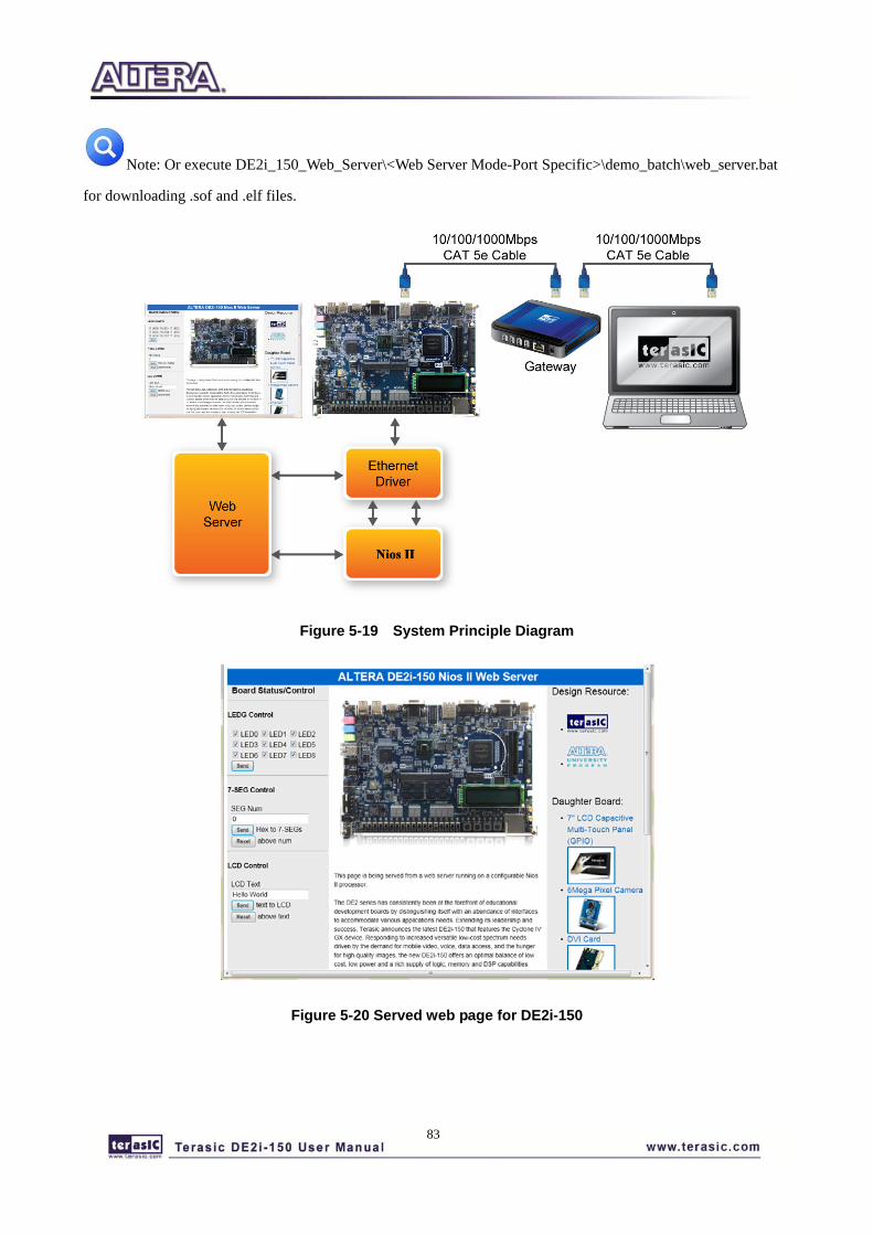
83
Note: Or execute DE2i_150_Web_Server\<Web Server Mode-Port Specific>\demo_batch\web_server.bat
for downloading .sof and .elf files.
Figure 5-19 System Principle Diagram
Figure 5-20 Served web page for DE2i-150
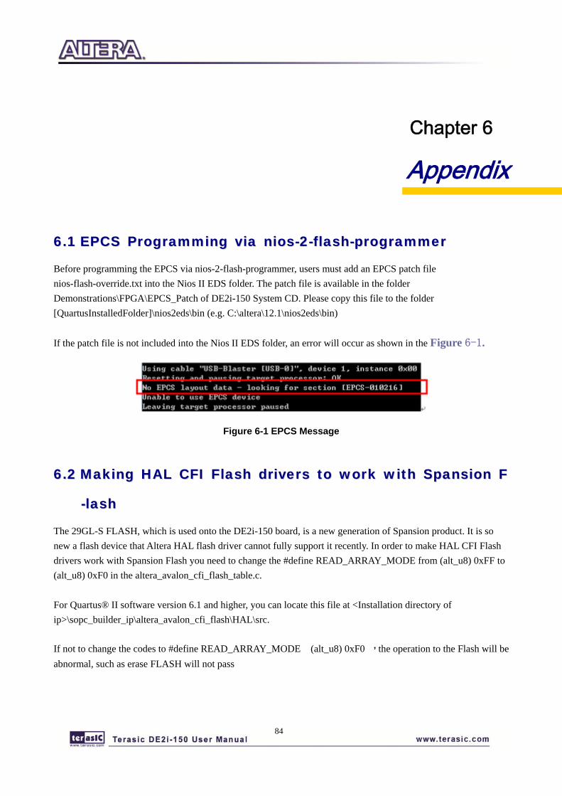
84
Chapter 6 Appendix
66..11 EEPPCCSS PPrrooggrraammmmiinngg vviiaa nniiooss--22--ffllaasshh--pprrooggrraammmmeerr
Before programming the EPCS via nios-2-flash-programmer, users must add an EPCS patch file nios-flash-override.txt into the Nios II EDS folder. The patch file is available in the folder Demonstrations\FPGA\EPCS_Patch of DE2i-150 System CD. Please copy this file to the folder [QuartusInstalledFolder]\nios2eds\bin (e.g. C:\altera\12.1\nios2eds\bin) If the patch file is not included into the Nios II EDS folder, an error will occur as shown in the Figure 6-1.
Figure 6-1 EPCS Message
66..22 MMaakkiinngg HHAALL CCFFII FFllaasshh ddrriivveerrss ttoo wwoorrkk wwiitthh SSppaannssiioonn FF
--llaasshh
The 29GL-S FLASH, which is used onto the DE2i-150 board, is a new generation of Spansion product. It is so new a flash device that Altera HAL flash driver cannot fully support it recently. In order to make HAL CFI Flash drivers work with Spansion Flash you need to change the #define READ_ARRAY_MODE from (alt_u8) 0xFF to (alt_u8) 0xF0 in the altera_avalon_cfi_flash_table.c. For Quartus® II software version 6.1 and higher, you can locate this file at <Installation directory of ip>\sopc_builder_ip\altera_avalon_cfi_flash\HAL\src. If not to change the codes to #define READ_ARRAY_MODE (alt_u8) 0xF0 ,the operation to the Flash will be abnormal, such as erase FLASH will not pass
85
66..33 RReevviissiioonn HHiissttoorryy
Version Change Log V1.0 Initial Version (Preliminary)
66..44 CCooppyyrriigghhtt SSttaatteemmeenntt
Copyright © 2013 Terasic Technologies. All rights reserved.