Embed Size (px)
Citation preview

DDR4 Mini WorkshopDDR4 Mini WorkshopDDR4 Mini WorkshopDDR4 Mini Workshop
Server Memory Forum 2011Server Memory Forum 2011

DisclaimerDisclaimer
E th h M j it f DDR4 h b d fi d/Fi d thEven though Majority of DDR4 spec has been defined/Fixed, there might be chance of update before publicationt
Rev A is expected to be in publice 1H’12 and the contents of this material might be changed in Final versiong g

DDR4 OutlookDDR4 OutlookDDR4 adopts evolutionary path with High BW & reliability schemeDDR4 adopts evolutionary path with High BW & reliability scheme
Spec items DDR3 DDR4
D it / S d 512Mbp~8Gb 2Gb~16GbDensity / Speed 512Mbp 8Gb1.6~2.1Gbps
2Gb 16Gb1.6~3.2Gbps
Voltage(VDD/VDDQ/VPP)
1.5V/1.5V/NA(1.35V/1.35V/NA) 1.2V/1.2V/2.5V
Vref External Vref (VDD/2) Internal Vref (need training)Interface
Vref External Vref (VDD/2) Internal Vref (need training)
Data IO CTT (34ohm) POD (34ohm)
CMD/ADDR IO CTT CTT
Strobe Bi-dir / diff Bi-dir / diffStrobe Bi dir / diff Bi dir / diff
Core architect
# of banks 8Banks 16Banks (4BG)
Page size(X4/8/16) 1KB / 1KB / 2KB 512B / 1KB / 2KBarchitect
# prefetch 8bits 8bits
Added function RESET/ZQ/Dynamic ODT + CRC/DBI/Multi preamble ..
Package type/balls (X4 8/X16) 78 / 96 BGA 78 / 96 BGA
Physical(X4,8/X16) 78 / 96 BGA 78 / 96 BGA
DIMM type R,LR,U,SoDIMM + ECC SoDIMM
DIMM pins 240 (R,LR,U) / 204 (So) 284 (R,LR,U) / 256 (So)

Bank Group alleviates the needs to increase core frequency from Bank GroupBank Group
p q yprevious gen. products to DDR4
DDR DDR2 DDR3 DDR4BL 2 4 8 8 with BG
Bank 0 Bank 4
Group 0 Group 1Bank 0 Bank 0
Group 0
BL 2 4 8 8 with BG
Core freq. 200MHz 200MHz 200MHz 200MHz
Bank 0
Bank 1
Bank 2
Bank 4
Bank 5
Bank 6
Bank 0
Bank 1
Bank 2
Bank 0
Bank 1
Bank 2
Bank 3Sense Amp
Bank 7Sense Amp
32/64bit32/64bit
32/64bit32/64bit
Bank 3Sense Amp
Bank 3Sense Amp
64bit64bit
64bit64bit
Bank 8
Bank 9
Sense AmpBank 12
Bank 13
Sense Amp
Bank 4
Bank 5
Sense AmpBank 4
Bank 5
Sense Amp
Bank 10
Bank 11
Bank 14
Bank 15
Group 2 Group 3
Bank 6
Bank 7
Bank 6
Bank 7
Group 1<X4/X8 16 B k ith 4 B k G > <X16 8 B k ith 2 B k G ><X4/X8: 16 Banks with 4 Bank Group> <X16: 8 Banks with 2 Bank Group>
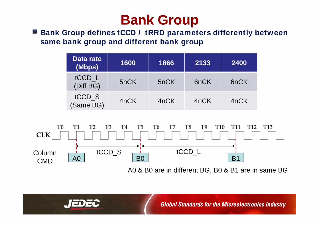
Bank Group defines tCCD / tRRD parameters differently between Bank GroupBank Group
p / p ysame bank group and different bank group
Data rate 1600 1866 2133 2400(Mbps) 1600 1866 2133 2400
tCCD_L(Diff BG) 5nCK 5nCK 6nCK 6nCK(Diff BG)tCCD_S
(Same BG) 4nCK 4nCK 4nCK 4nCK
ColumnCMD A0 B0 B1
tCCD_S tCCD_L
A0 & B0 are in different BG, B0 & B1 are in same BG

Fine GranularityFine Granularity RefreshRefreshAs density increases, tRFC gets longer and limits performancey , g g pAdded new function supporting X2/X4 more frequent refresh with shorter tRFC
Fine granularity refresh shows better performanceFine granularity refresh shows better performance
Case: 2Gb based 2Rank system Source : IBM JEDEC material

DDR4 supports WRITE CRC to assure better reliability in system
CRCCRC(Cyclic Redundancy(Cyclic Redundancy Check)Check)DDR4 supports WRITE CRC to assure better reliability in system
Data bits are followed by CRC bits
<CRC data bit mapping for x8 device> <CRC data bit mapping for x4 device>
CRC polynomial is the ATM-8 HEC (X^8+X^2+X^1+1) and 8 CRCbits are generated from 72 data+DBI bits
Same polynomial as GDDR5In BC4 case, chopped 4UI will be treated as “1”With CRC enabled, using burst ordering with A0:A1 is limited (Fixed to 0:0)
- 7

CRC fi i i f il d li b li bili
CRCCRC(Cyclic Redundancy(Cyclic Redundancy Check)Check)CRC fixes intermittent failure and realizes better system reliabilityAbout 10% of performance gain is expected
A 0 0 0 0 0 0 0 0 0 0 0 0 0 0 0 0 0 0 0 0 0B 0 0 0 0 0 0 0 0 0 0 0 0 0 0 0 0 0 0 0 0 0C 0 0 0 0 0 0 0 0 0 0 0 0 0 0 0 0 0 0 0 0 0C 0 0 0 0 0 0 0 0 0 0 0 0 0 0 0 0 0 0 0 0 0D 0 0 0 0 0 0 0 0 0 0 0 0 0 0 0 0 0 0 0 0 0E 0 0 0 0 0 0 0 0 0 0 0 0 0 0 0 0 0 0 0 0 0F 0 0 0 0 0 0 0 0 0 0 0 0 0 0 0 0 0 0 0 0 0G 0 0 0 0 0 0 0 0 0 0 0 0 0 0 0 0 0 0 0 0 0H 0 0 0 0 0 0 0 0 0 1 0 0 0 0 0 0 0 0 0 0 0C
hann
el
I 0 0 0 0 0 0 0 0 0 0 0 0 0 0 0 0 0 0 0 0 0J 0 0 0 0 0 0 0 0 0 0 0 0 0 0 0 0 0 0 0 0 0
Frequency 1900 1910 1920 1930 1940 1950 1960 1970 1980 1990 2000 2010 2020 2030 2040 2050 2060 2070 2080 2090 2100
Channel Intermittent failure Freq(MHz)Channel Intermittent failure q( )
- 8
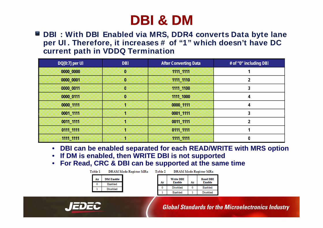
DBIDBI & DM& DMDBI : With DBI Enabled via MRS, DDR4 converts Data byte lane
DQ[0 7] UI DBI Aft C ti D t # f “0” i l di DBI
DBI : With DBI Enabled via MRS, DDR4 converts Data byte lane per UI. Therefore, it increases # of “1” which doesn’t have DC current path in VDDQ Termination
DQ[0:7] per UI DBI After Converting Data # of “0” including DBI
0000_0000 0 1111_1111 1
0000_0001 0 1111_1110 2
0000 0011 0 1111 1100 30000_0011 0 1111_1100 3
0000_0111 0 1111_1000 4
0000_1111 1 0000_1111 4
0001 1111 1 0001 1111 30001_1111 1 0001_1111 3
0011_1111 1 0011_1111 2
0111_1111 1 0111_1111 1
1111 1111 1 1111 1111 0_ _ 0
• DBI can be enabled separated for each READ/WRITE with MRS option• If DM is enabled, then WRITE DBI is not supported• For Read, CRC & DBI can be supported at the same time, pp

The following is example of training @initialization based upon
High Level Training/Calibration FlowHigh Level Training/Calibration FlowThe following is example of training @initialization based upon supported function in JEDEC spec
Actual training/calibration sequence would be different depending on controllerE t d DDR4 Fl
Current Typical DDR3 System Example
Expected DDR4 Flow
Power UpPower Up
Power Up
MRS Setting
MRS Setting
ZQ Calibration
ZQ Calibration
ZQ Calibration
Leveling(Read Write)
Leveling(Read Write)
( )
IO Training
More MPR Pattern (832)
IO TrainingVref Training
Preamble Training
DQ training w/ MPRg

Calibration/Training : Calibration/Training : VrefVref & & DQDQDDR4 changed data line termination from CTT to POD to save IO Powersave IO Power
One downside of POD in multiple DIMMconfiguration, Vref level in each rank might be different
[source: DDR4 TG]
g
Therefore, DDR4 has internal VrefDQ which requires trainingVrefDQ which requires training from Host which requires at initialization
f S /Vref Step increase/decrease will be controlled via MRS Opcode1 Vref Step size is 0.65% of VDDQ1 St lti l t i /d1 Step or multiple step increase/decrease is allowed for efficient calibration time

Calibration/Training : Preamble Training, Calibration/Training : Preamble Training, MPRMPRDDR4 supports READ Preamble Training via MRS to have better
Host enables Rx @ 1st edge : the edge will be different
DDR4 supports READ Preamble Training via MRS to have better fine alignment of HOST Rx enable time
With this mode, Host can detect when Host Rx should be enabled to get READ Data from DRAM Host enables Rx @ 1 edge : the edge will be different
depending on board configuration
DDR4 assigned more MPR for DQ training and also it’s Re-writable
DDR3 MPR is Read onlyDDR3 DDR4 Note
# of MPR 8Bits (1Register) 32bits (4Register)
Predefined Pattern 01010101
MPR0: 01010101MPR1: 00110011MPR2: 00001111MPR3: 00000000

Calibration/Training : Preamble Training, Calibration/Training : Preamble Training, MPRMPRDDR4 Supports 3 way of DQ Link Training with 4 MPR as follows
1) Serial Readout : Predefined pattern or Re-writed pattern is returned to Host Serial
2) Parallel Readout : Predefined pattern or Re-writed pattern is returned to Host Parallel manner
DDR4 Supports 3 way of DQ Link Training with 4 MPR as follows
pmanner
3) Staggered Readout : Predefined pattern or Re-writed pattern is returned to Host Staggered manner as following
Stagger UI0-7 UI8-15 UI16-23 UI24-31 UI32-39 UI40-47 UI48-55 UI56-63DQ0 MPR0 MPR1 MPR2 MPR3 MPR0 MPR1 MPR2 MPR3DQ1 MPR1 MPR2 MPR3 MPR0 MPR1 MPR2 MPR3 MPR0DQ2 MPR2 MPR3 MPR0 MPR1 MPR2 MPR3 MPR0 MPR1DQ3 MPR3 MPR0 MPR1 MPR2 MPR3 MPR0 MPR1 MPR2DQ4 MPR0 MPR1 MPR2 MPR3 MPR0 MPR1 MPR2 MPR3DQ5 MPR1 MPR2 MPR3 MPR0 MPR1 MPR2 MPR3 MPR0DQ6 MPR2 MPR3 MPR0 MPR1 MPR2 MPR3 MPR0 MPR1DQ7 MPR3 MPR0 MPR1 MPR2 MPR3 MPR0 MPR1 MPR2
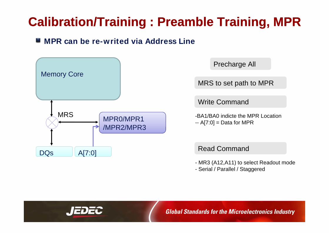
Calibration/Training : Preamble Training, Calibration/Training : Preamble Training, MPRMPRMPR can be re-writed via Address Line
Precharge AllMemory Core
Precharge All
MRS to set path to MPR
MPR0/MPR1MRS
Write Command
-BA1/BA0 indicte the MPR LocationMPR0/MPR1/MPR2/MPR3
MRS -BA1/BA0 indicte the MPR Location-- A[7:0] = Data for MPR
DQs [ ]A[7:0] Read Command
- MR3 (A12,A11) to select Readout mode- Serial / Parallel / Staggered- Serial / Parallel / Staggered