Embed Size (px)
Citation preview
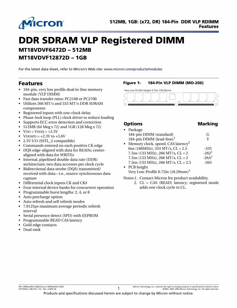
512MB, 1GB: (x72, DR) 184-Pin DDR VLP RDIMMFeatures
DDR SDRAM VLP Registered DIMMMT18VDVF6472D – 512MBMT18VDVF12872D – 1GB
For the latest data sheet, refer to Micron’s Web site: www.micron.com/products/modules
Features• 184-pin, very low profile dual in-line memory
module (VLP DIMM)• Fast data transfer rates: PC2100 or PC2700• Utilizes 266 MT/s and 333 MT/s DDR SDRAM
components• Registered inputs with one-clock delay• Phase-lock loop (PLL) clock driver to reduce loading• Supports ECC error detection and correction• 512MB (64 Meg x 72) and 1GB (128 Meg x 72)• VDD = VDDQ = +2.5V• VDDSPD = +2.3V to +3.6V• 2.5V I/O (SSTL_2 compatible)• Commands entered on each positive CK edge• DQS edge-aligned with data for READs; center-
aligned with data for WRITEs• Internal, pipelined double data rate (DDR)
architecture; two data accesses per clock cycle• Bidirectional data strobe (DQS) transmitted/
received with data—i.e., source-synchronous data capture
• Differential clock inputs CK and CK# • Four internal device banks for concurrent operation• Programmable burst lengths: 2, 4, or 8• Auto precharge option• Auto refresh and self refresh modes• 7.8125µs maximum average periodic refresh
interval• Serial presence detect (SPD) with EEPROM• Programmable READ CAS latency• Gold edge contacts• Dual rank
Products and specifications discussed herein are
PDF: 09005aef81c73825/Source: 09005aef81c73837DVF18C64_128x72D_1.fm - Rev. A 8/05 EN 1
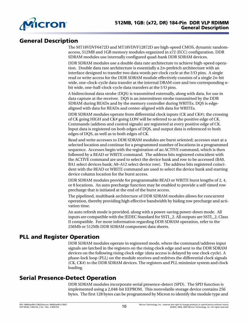
Figure 1: 184-Pin VLP DIMM (MO-206)
Notes:1. Contact Micron for product availability.2. CL = CAS (READ) latency; registered mode
adds one clock cycle to CL.
Options Marking• Package
184-pin DIMM (standard) G184-pin DIMM (lead-free)1 Y
• Memory clock, speed, CAS latency2
6ns (166MHz), 333 MT/s, CL = 2.5 -3357.5ns (133 MHz), 266 MT/s, CL = 2 -2621
7.5ns (133 MHz), 266 MT/s, CL = 2 -26A1
7.5ns (133 MHz), 266 MT/s, CL = 2.5 -265• PCB height
Very Low-Profile 0.72in (18.29mm)1
Very Low Profile Height 0.72in (18.29mm)
subject to change by Micron without notice.
Micron Technology, Inc., reserves the right to change products or specifications without notice.©2003, 2004, 2005 Micron Technology, Inc. All rights reserved.
512MB, 1GB: (x72, DR) 184-Pin DDR VLP RDIMMFeatures
Note: All part numbers end with a two-place code (not shown), designating component and PCB revisions. Consult factory for current revision codes. Example: MT18VDVF6472DY-265B1.
Table 1: Address Table
512MB 1GB
Refresh Count 8K 8K
Row Addressing 8K (A0–A12) 8K (A0–A12)
Device Bank Addressing 4 (BA0, BA1) 4 (BA0, BA1)
Device Configuration 256Mb (32 Meg x 8) 512Mb (64 Meg x 8)
Column Addressing 1K (A0–A9) 2K (A0–A9, A11)
Module Rank Addressing 2 (S0#, S1#) 2 (S0#, S1#)
Table 2: Part Numbers and Timing Parameters
Part Number Module Density
Configuration Module Bandwidth
Memory Clock/Data Rate
Latency (CL - tRCD - tRP)
MT18VDVF6472DG-335__ 512MB 64 Meg x 72 2.7 GB/s 6ns/333 MT/s 2.5-3-3
MT18VDVF6472DY-335__ 512MB 64 Meg x 72 2.7 GB/s 6ns/333 MT/s 2.5-3-3
MT18VDVF6472DG-262__ 512MB 64 Meg x 72 2.1 GB/s 7.5ns/266 MT/s 2-2-2
MT18VDVF6472DY-262__ 512MB 64 Meg x 72 2.1 GB/s 7.5ns/266 MT/s 2-2-2
MT18VDVF6472DG-26A__ 512MB 64 Meg x 72 2.1 GB/s 7.5ns/266 MT/s 2-3-3
MT18VDVF6472DY-26A__ 512MB 64 Meg x 72 2.1 GB/s 7.5ns/266 MT/s 2-3-3
MT18VDVF6472DG-265__ 512MB 64 Meg x 72 2.1 GB/s 7.5ns/266 MT/s 2.5-3-3
MT18VDVF6472DY-265__ 512MB 64 Meg x 72 2.1 GB/s 7.5ns/266 MT/s 2.5-3-3
MT18VDVF6472DG-202__ 512MB 64 Meg x 72 1.6 GB/s 10ns/200 MT/s 2-2-2
MT18VDVF6472DY-202__ 512MB 64 Meg x 72 1.6 GB/s 10ns/200 MT/s 2-2-2
MT18VDVF12872DG-335__ 1GB 128 Meg x 72 2.7 GB/s 6ns/333 MT/s 2.5-3-3
MT18VDVF12872DY-335__ 1GB 128 Meg x 72 2.7 GB/s 6ns/333 MT/s 2.5-3-3
MT18VDVF12872DG-262__ 1GB 128 Meg x 72 2.1 GB/s 7.5ns/266 MT/s 2-2-2
MT18VDVF12872DY-262__ 1GB 128 Meg x 72 2.1 GB/s 7.5ns/266 MT/s 2-2-2
MT18VDVF12872DG-26A__ 1GB 128 Meg x 72 2.1 GB/s 7.5ns/266 MT/s 2-3-3
MT18VDVF12872DY-26A__ 1GB 128 Meg x 72 2.1 GB/s 7.5ns/266 MT/s 2-3-3
MT18VDVF12872DG-265__ 1GB 128 Meg x 72 2.1 GB/s 7.5ns/266 MT/s 2.5-3-3
MT18VDVF12872DY-265__ 1GB 128 Meg x 72 2.1 GB/s 7.5ns/266 MT/s 2.5-3-3
MT18VDVF12872DG-202__ 1GB 128 Meg x 72 1.6 GB/s 10ns/200 MT/s 2-2-2
MT18VDVF12872DY-202__ 1GB 128 Meg x 72 1.6 GB/s 10ns/200 MT/s 2-2-2
PDF: 09005aef81c73825/Source: 09005aef81c73837 Micron Technology, Inc., reserves the right to change products or specifications without notice.DVF18C64_128x72D_1.fm - Rev. A 8/05 EN 2 ©2003, 2004, 2005 Micron Technology, Inc. All rights reserved.
PDF: 09005aef81c73825/Source: 09005aef81c73837 Micron Technology, Inc., reserves the right to change products or specifications without notice.DVF18C64_128x72DTOC.fm - Rev. A 8/05 EN 3 ©2003, 2004, 2005 Micron Technology, Inc. All rights reserved.
512MB, 1GB: (x72, DR) 184-Pin DDR VLP RDIMMTable of Contents
Table of ContentsFeatures . . . . . . . . . . . . . . . . . . . . . . . . . . . . . . . . . . . . . . . . . . . . . . . . . . . . . . . . . . . . . . . . . . . . . . . . . . . . . . . . . . . . . . . . . . . . . .1Table of Contents . . . . . . . . . . . . . . . . . . . . . . . . . . . . . . . . . . . . . . . . . . . . . . . . . . . . . . . . . . . . . . . . . . . . . . . . . . . . . . . . . . . . .3List of Figures . . . . . . . . . . . . . . . . . . . . . . . . . . . . . . . . . . . . . . . . . . . . . . . . . . . . . . . . . . . . . . . . . . . . . . . . . . . . . . . . . . . . . . . . .4List of Tables. . . . . . . . . . . . . . . . . . . . . . . . . . . . . . . . . . . . . . . . . . . . . . . . . . . . . . . . . . . . . . . . . . . . . . . . . . . . . . . . . . . . . . . . . .5Pin Assignments and Descriptions . . . . . . . . . . . . . . . . . . . . . . . . . . . . . . . . . . . . . . . . . . . . . . . . . . . . . . . . . . . . . . . . . . . . . .6Functional Block Diagrams. . . . . . . . . . . . . . . . . . . . . . . . . . . . . . . . . . . . . . . . . . . . . . . . . . . . . . . . . . . . . . . . . . . . . . . . . . . . .9General Description . . . . . . . . . . . . . . . . . . . . . . . . . . . . . . . . . . . . . . . . . . . . . . . . . . . . . . . . . . . . . . . . . . . . . . . . . . . . . . . . . .10PLL and Register Operation . . . . . . . . . . . . . . . . . . . . . . . . . . . . . . . . . . . . . . . . . . . . . . . . . . . . . . . . . . . . . . . . . . . . . . . . . . .10Serial Presence-Detect Operation . . . . . . . . . . . . . . . . . . . . . . . . . . . . . . . . . . . . . . . . . . . . . . . . . . . . . . . . . . . . . . . . . . . . . .10Mode Register Definition . . . . . . . . . . . . . . . . . . . . . . . . . . . . . . . . . . . . . . . . . . . . . . . . . . . . . . . . . . . . . . . . . . . . . . . . . . . . .11
Burst Length . . . . . . . . . . . . . . . . . . . . . . . . . . . . . . . . . . . . . . . . . . . . . . . . . . . . . . . . . . . . . . . . . . . . . . . . . . . . . . . . . . . . . .11Burst Type . . . . . . . . . . . . . . . . . . . . . . . . . . . . . . . . . . . . . . . . . . . . . . . . . . . . . . . . . . . . . . . . . . . . . . . . . . . . . . . . . . . . . . . .11Read Latency . . . . . . . . . . . . . . . . . . . . . . . . . . . . . . . . . . . . . . . . . . . . . . . . . . . . . . . . . . . . . . . . . . . . . . . . . . . . . . . . . . . . . .12Operating Mode . . . . . . . . . . . . . . . . . . . . . . . . . . . . . . . . . . . . . . . . . . . . . . . . . . . . . . . . . . . . . . . . . . . . . . . . . . . . . . . . . . .14
Extended Mode Register . . . . . . . . . . . . . . . . . . . . . . . . . . . . . . . . . . . . . . . . . . . . . . . . . . . . . . . . . . . . . . . . . . . . . . . . . . . . . .14DLL Enable/Disable. . . . . . . . . . . . . . . . . . . . . . . . . . . . . . . . . . . . . . . . . . . . . . . . . . . . . . . . . . . . . . . . . . . . . . . . . . . . . . . .15
Commands . . . . . . . . . . . . . . . . . . . . . . . . . . . . . . . . . . . . . . . . . . . . . . . . . . . . . . . . . . . . . . . . . . . . . . . . . . . . . . . . . . . . . . . . . .16Absolute Maximum Ratings . . . . . . . . . . . . . . . . . . . . . . . . . . . . . . . . . . . . . . . . . . . . . . . . . . . . . . . . . . . . . . . . . . . . . . . . . . .17Electrical Specifications. . . . . . . . . . . . . . . . . . . . . . . . . . . . . . . . . . . . . . . . . . . . . . . . . . . . . . . . . . . . . . . . . . . . . . . . . . . . . . .18Notes . . . . . . . . . . . . . . . . . . . . . . . . . . . . . . . . . . . . . . . . . . . . . . . . . . . . . . . . . . . . . . . . . . . . . . . . . . . . . . . . . . . . . . . . . . . . . . .22Initialization . . . . . . . . . . . . . . . . . . . . . . . . . . . . . . . . . . . . . . . . . . . . . . . . . . . . . . . . . . . . . . . . . . . . . . . . . . . . . . . . . . . . . . . . .27Register and PLL Specifications . . . . . . . . . . . . . . . . . . . . . . . . . . . . . . . . . . . . . . . . . . . . . . . . . . . . . . . . . . . . . . . . . . . . . . . .29Temperature and Air Flow Specifications . . . . . . . . . . . . . . . . . . . . . . . . . . . . . . . . . . . . . . . . . . . . . . . . . . . . . . . . . . . . . . .31Serial Presence-Detect . . . . . . . . . . . . . . . . . . . . . . . . . . . . . . . . . . . . . . . . . . . . . . . . . . . . . . . . . . . . . . . . . . . . . . . . . . . . . . . .32
SPD Clock And Data Conventions . . . . . . . . . . . . . . . . . . . . . . . . . . . . . . . . . . . . . . . . . . . . . . . . . . . . . . . . . . . . . . . . . . .32SPD Start Condition. . . . . . . . . . . . . . . . . . . . . . . . . . . . . . . . . . . . . . . . . . . . . . . . . . . . . . . . . . . . . . . . . . . . . . . . . . . . . . . .32SPD Stop Condition . . . . . . . . . . . . . . . . . . . . . . . . . . . . . . . . . . . . . . . . . . . . . . . . . . . . . . . . . . . . . . . . . . . . . . . . . . . . . . . .32SPD Acknowledge. . . . . . . . . . . . . . . . . . . . . . . . . . . . . . . . . . . . . . . . . . . . . . . . . . . . . . . . . . . . . . . . . . . . . . . . . . . . . . . . . .32
Module Dimensions . . . . . . . . . . . . . . . . . . . . . . . . . . . . . . . . . . . . . . . . . . . . . . . . . . . . . . . . . . . . . . . . . . . . . . . . . . . . . . . . . .38Data Sheet Designation . . . . . . . . . . . . . . . . . . . . . . . . . . . . . . . . . . . . . . . . . . . . . . . . . . . . . . . . . . . . . . . . . . . . . . . . . . . . . . .38
PDF: 09005aef81c73825/Source: 09005aef81c73837 Micron Technology, Inc., reserves the right to change products or specifications without notice.DVF18C64_128x72DLOF.fm - Rev. A 8/05 EN 4 ©2003, 2004, 2005 Micron Technology, Inc. All rights reserved.
512MB, 1GB: (x72, DR) 184-Pin DDR VLP RDIMMList of Figures
List of FiguresFigure 1: 184-Pin VLP DIMM (MO-206) . . . . . . . . . . . . . . . . . . . . . . . . . . . . . . . . . . . . . . . . . . . . . . . . . . . . . . . . . . . . . .1Figure 2: Pin Locations . . . . . . . . . . . . . . . . . . . . . . . . . . . . . . . . . . . . . . . . . . . . . . . . . . . . . . . . . . . . . . . . . . . . . . . . . . . . .6Figure 3: Very Low Profile DIMM Functional Block Diagram . . . . . . . . . . . . . . . . . . . . . . . . . . . . . . . . . . . . . . . . . . .9Figure 4: Mode Register Definition Diagram . . . . . . . . . . . . . . . . . . . . . . . . . . . . . . . . . . . . . . . . . . . . . . . . . . . . . . . .12Figure 5: CAS Latency Diagram . . . . . . . . . . . . . . . . . . . . . . . . . . . . . . . . . . . . . . . . . . . . . . . . . . . . . . . . . . . . . . . . . . . .14Figure 6: Extended Mode Register Definition Diagram . . . . . . . . . . . . . . . . . . . . . . . . . . . . . . . . . . . . . . . . . . . . . . .15Figure 7: Derating Data Valid Window (tQH - tDQSQ) . . . . . . . . . . . . . . . . . . . . . . . . . . . . . . . . . . . . . . . . . . . . . . . 24Figure 8: Pull-Down . . . . . . . . . . . . . . . . . . . . . . . . . . . . . . . . . . . . . . . . . . . . . . . . . . . . . . . . . . . . . . . . . . . . . . . . . . . . . .25Figure 9: Pull-Up . . . . . . . . . . . . . . . . . . . . . . . . . . . . . . . . . . . . . . . . . . . . . . . . . . . . . . . . . . . . . . . . . . . . . . . . . . . . . . . . .25Figure 10: Initialization Flow Diagram . . . . . . . . . . . . . . . . . . . . . . . . . . . . . . . . . . . . . . . . . . . . . . . . . . . . . . . . . . . . . . .28Figure 11: Component Case Temperature vs. Air Flow . . . . . . . . . . . . . . . . . . . . . . . . . . . . . . . . . . . . . . . . . . . . . . . . .31Figure 12: Data Validity . . . . . . . . . . . . . . . . . . . . . . . . . . . . . . . . . . . . . . . . . . . . . . . . . . . . . . . . . . . . . . . . . . . . . . . . . . . .32Figure 13: Definition of Start and Stop . . . . . . . . . . . . . . . . . . . . . . . . . . . . . . . . . . . . . . . . . . . . . . . . . . . . . . . . . . . . . . .33Figure 14: Acknowledge Response From Receiver . . . . . . . . . . . . . . . . . . . . . . . . . . . . . . . . . . . . . . . . . . . . . . . . . . . . .33Figure 15: SPD EEPROM Timing Diagram . . . . . . . . . . . . . . . . . . . . . . . . . . . . . . . . . . . . . . . . . . . . . . . . . . . . . . . . . . . .34Figure 16: 184-Pin VLP RDIMM Dimensions. . . . . . . . . . . . . . . . . . . . . . . . . . . . . . . . . . . . . . . . . . . . . . . . . . . . . . . . . .38
PDF: 09005aef81c73825/Source: 09005aef81c73837 Micron Technology, Inc., reserves the right to change products or specifications without notice.DVF18C64_128x72DLOT.fm - Rev. A 8/05 EN 5 ©2003, 2004, 2005 Micron Technology, Inc. All rights reserved.
512MB, 1GB: (x72, DR) 184-Pin DDR VLP RDIMMList of Tables
List of TablesTable 1: Address Table . . . . . . . . . . . . . . . . . . . . . . . . . . . . . . . . . . . . . . . . . . . . . . . . . . . . . . . . . . . . . . . . . . . . . . . . . . . .2Table 2: Part Numbers and Timing Parameters . . . . . . . . . . . . . . . . . . . . . . . . . . . . . . . . . . . . . . . . . . . . . . . . . . . . . .2Table 3: Pin Assignment . . . . . . . . . . . . . . . . . . . . . . . . . . . . . . . . . . . . . . . . . . . . . . . . . . . . . . . . . . . . . . . . . . . . . . . . . . .6Table 4: Pin Descriptions . . . . . . . . . . . . . . . . . . . . . . . . . . . . . . . . . . . . . . . . . . . . . . . . . . . . . . . . . . . . . . . . . . . . . . . . . .7Table 5: Burst Definition Table . . . . . . . . . . . . . . . . . . . . . . . . . . . . . . . . . . . . . . . . . . . . . . . . . . . . . . . . . . . . . . . . . . . .13Table 6: CAS Latency Table . . . . . . . . . . . . . . . . . . . . . . . . . . . . . . . . . . . . . . . . . . . . . . . . . . . . . . . . . . . . . . . . . . . . . . .13Table 7: Commands Truth Table . . . . . . . . . . . . . . . . . . . . . . . . . . . . . . . . . . . . . . . . . . . . . . . . . . . . . . . . . . . . . . . . . .16Table 8: DM Operation Truth Table. . . . . . . . . . . . . . . . . . . . . . . . . . . . . . . . . . . . . . . . . . . . . . . . . . . . . . . . . . . . . . . .16Table 9: DC Electrical Characteristics and Operating Conditions. . . . . . . . . . . . . . . . . . . . . . . . . . . . . . . . . . . . . .17Table 10: AC Input Operating Conditions. . . . . . . . . . . . . . . . . . . . . . . . . . . . . . . . . . . . . . . . . . . . . . . . . . . . . . . . . . . .17Table 11: IDD Specifications and Conditions – 512MB. . . . . . . . . . . . . . . . . . . . . . . . . . . . . . . . . . . . . . . . . . . . . . . . .18Table 12: IDD Specifications and Conditions – 1GB . . . . . . . . . . . . . . . . . . . . . . . . . . . . . . . . . . . . . . . . . . . . . . . . . . .19Table 13: Capacitance (512MB only) . . . . . . . . . . . . . . . . . . . . . . . . . . . . . . . . . . . . . . . . . . . . . . . . . . . . . . . . . . . . . . . .20Table 14: Electrical Characteristics and Recommended AC Operating Conditions . . . . . . . . . . . . . . . . . . . . . . .20Table 15: Register Timing Requirements and Switching Characteristics. . . . . . . . . . . . . . . . . . . . . . . . . . . . . . . . .29Table 16: PLL Clock Driver Timing Requirements and Switching Characteristics . . . . . . . . . . . . . . . . . . . . . . . .30Table 17: EEPROM Device Select Code . . . . . . . . . . . . . . . . . . . . . . . . . . . . . . . . . . . . . . . . . . . . . . . . . . . . . . . . . . . . . .34Table 18: EEPROM Operating Modes . . . . . . . . . . . . . . . . . . . . . . . . . . . . . . . . . . . . . . . . . . . . . . . . . . . . . . . . . . . . . . .34Table 19: Serial Presence-Detect EEPROM DC Operating Conditions. . . . . . . . . . . . . . . . . . . . . . . . . . . . . . . . . . .35Table 20: Serial Presence-Detect EEPROM AC Operating Conditions . . . . . . . . . . . . . . . . . . . . . . . . . . . . . . . . . . .35Table 21: Serial Presence-Detect Matrix . . . . . . . . . . . . . . . . . . . . . . . . . . . . . . . . . . . . . . . . . . . . . . . . . . . . . . . . . . . . .36
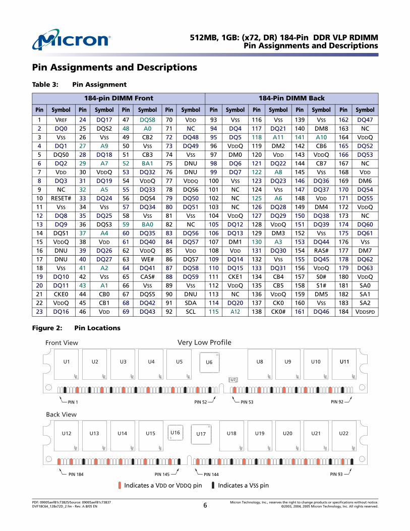
512MB, 1GB: (x72, DR) 184-Pin DDR VLP RDIMMPin Assignments and Descriptions
Pin Assignments and Descriptions
Figure 2: Pin Locations
Table 3: Pin Assignment
184-pin DIMM Front 184-Pin DIMM Back
Pin Symbol Pin Symbol Pin Symbol Pin Symbol Pin Symbol Pin Symbol Pin Symbol Pin Symbol
1 VREF 24 DQ17 47 DQS8 70 VDD 93 VSS 116 VSS 139 VSS 162 DQ472 DQ0 25 DQS2 48 A0 71 NC 94 DQ4 117 DQ21 140 DM8 163 NC3 VSS 26 VSS 49 CB2 72 DQ48 95 DQ5 118 A11 141 A10 164 VDDQ4 DQ1 27 A9 50 VSS 73 DQ49 96 VDDQ 119 DM2 142 CB6 165 DQ525 DQS0 28 DQ18 51 CB3 74 VSS 97 DM0 120 VDD 143 VDDQ 166 DQ536 DQ2 29 A7 52 BA1 75 DNU 98 DQ6 121 DQ22 144 CB7 167 NC7 VDD 30 VDDQ 53 DQ32 76 DNU 99 DQ7 122 A8 145 VSS 168 VDD
8 DQ3 31 DQ19 54 VDDQ 77 VDDQ 100 VSS 123 DQ23 146 DQ36 169 DM69 NC 32 A5 55 DQ33 78 DQS6 101 NC 124 VSS 147 DQ37 170 DQ5410 RESET# 33 DQ24 56 DQS4 79 DQ50 102 NC 125 A6 148 VDD 171 DQ5511 VSS 34 VSS 57 DQ34 80 DQ51 103 NC 126 DQ28 149 DM4 172 VDDQ12 DQ8 35 DQ25 58 VSS 81 VSS 104 VDDQ 127 DQ29 150 DQ38 173 NC13 DQ9 36 DQS3 59 BA0 82 NC 105 DQ12 128 VDDQ 151 DQ39 174 DQ6014 DQS1 37 A4 60 DQ35 83 DQ56 106 DQ13 129 DM3 152 VSS 175 DQ6115 VDDQ 38 VDD 61 DQ40 84 DQ57 107 DM1 130 A3 153 DQ44 176 VSS
16 DNU 39 DQ26 62 VDDQ 85 VDD 108 VDD 131 DQ30 154 RAS# 177 DM717 DNU 40 DQ27 63 WE# 86 DQS7 109 DQ14 132 VSS 155 DQ45 178 DQ6218 VSS 41 A2 64 DQ41 87 DQ58 110 DQ15 133 DQ31 156 VDDQ 179 DQ6319 DQ10 42 VSS 65 CAS# 88 DQ59 111 CKE1 134 CB4 157 S0# 180 VDDQ20 DQ11 43 A1 66 VSS 89 VSS 112 VDDQ 135 CB5 158 S1# 181 SA021 CKE0 44 CB0 67 DQS5 90 DNU 113 NC 136 VDDQ 159 DM5 182 SA122 VDDQ 45 CB1 68 DQ42 91 SDA 114 DQ20 137 CK0 160 VSS 183 SA223 DQ16 46 VDD 69 DQ43 92 SCL 115 A12 138 CK0# 161 DQ46 184 VDDSPD
U11U1 U2 U3 U4 U5 U6
U7
U8 U9 U10 U11
U16 U17U12 U13 U14 U15 U18 U19 U20 U21 U22
PIN 93PIN 144PIN 145PIN 184
PIN 1 PIN 52 PIN 53 PIN 92
Indicates a VDD or VDDQ pin Indicates a VSS pin
Front View
Back View
Very Low Profile
PDF: 09005aef81c73825/Source: 09005aef81c73837 Micron Technology, Inc., reserves the right to change products or specifications without notice.DVF18C64_128x72D_2.fm - Rev. A 8/05 EN 6 ©2003, 2004, 2005 Micron Technology, Inc. All rights reserved.
512MB, 1GB: (x72, DR) 184-Pin DDR VLP RDIMMPin Assignments and Descriptions
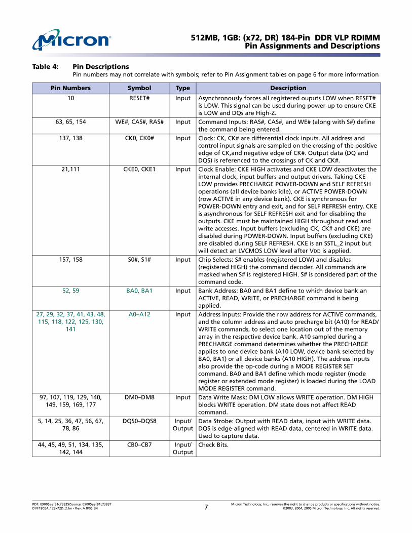
Table 4: Pin Descriptions Pin numbers may not correlate with symbols; refer to Pin Assignment tables on page 6 for more information
Pin Numbers Symbol Type Description
10 RESET# Input Asynchronously forces all registered ouputs LOW when RESET# is LOW. This signal can be used during power-up to ensure CKE is LOW and DQs are High-Z.
63, 65, 154 WE#, CAS#, RAS# Input Command Inputs: RAS#, CAS#, and WE# (along with S#) define the command being entered.
137, 138 CK0, CK0# Input Clock: CK, CK# are differential clock inputs. All address and control input signals are sampled on the crossing of the positive edge of CK,and negative edge of CK#. Output data (DQ and DQS) is referenced to the crossings of CK and CK#.
21,111 CKE0, CKE1 Input Clock Enable: CKE HIGH activates and CKE LOW deactivates the internal clock, input buffers and output drivers. Taking CKE LOW provides PRECHARGE POWER-DOWN and SELF REFRESH operations (all device banks idle), or ACTIVE POWER-DOWN (row ACTIVE in any device bank). CKE is synchronous for POWER-DOWN entry and exit, and for SELF REFRESH entry. CKE is asynchronous for SELF REFRESH exit and for disabling the outputs. CKE must be maintained HIGH throughout read and write accesses. Input buffers (excluding CK, CK# and CKE) are disabled during POWER-DOWN. Input buffers (excluding CKE) are disabled during SELF REFRESH. CKE is an SSTL_2 input but will detect an LVCMOS LOW level after VDD is applied.
157, 158 S0#, S1# Input Chip Selects: S# enables (registered LOW) and disables (registered HIGH) the command decoder. All commands are masked when S# is registered HIGH. S# is considered part of the command code.
52, 59 BA0, BA1 Input Bank Address: BA0 and BA1 define to which device bank an ACTIVE, READ, WRITE, or PRECHARGE command is being applied.
27, 29, 32, 37, 41, 43, 48, 115, 118, 122, 125, 130,
141
A0–A12 Input Address Inputs: Provide the row address for ACTIVE commands, and the column address and auto precharge bit (A10) for READ/WRITE commands, to select one location out of the memory array in the respective device bank. A10 sampled during a PRECHARGE command determines whether the PRECHARGE applies to one device bank (A10 LOW, device bank selected by BA0, BA1) or all device banks (A10 HIGH). The address inputs also provide the op-code during a MODE REGISTER SET command. BA0 and BA1 define which mode register (mode register or extended mode register) is loaded during the LOAD MODE REGISTER command.
97, 107, 119, 129, 140, 149, 159, 169, 177
DM0–DM8 Input Data Write Mask: DM LOW allows WRITE operation. DM HIGH blocks WRITE operation. DM state does not affect READ command.
5, 14, 25, 36, 47, 56, 67, 78, 86
DQS0–DQS8 Input/Output
Data Strobe: Output with READ data, input with WRITE data. DQS is edge-aligned with READ data, centered in WRITE data. Used to capture data.
44, 45, 49, 51, 134, 135, 142, 144
CB0–CB7 Input/Output
Check Bits.
PDF: 09005aef81c73825/Source: 09005aef81c73837 Micron Technology, Inc., reserves the right to change products or specifications without notice.DVF18C64_128x72D_2.fm - Rev. A 8/05 EN 7 ©2003, 2004, 2005 Micron Technology, Inc. All rights reserved.
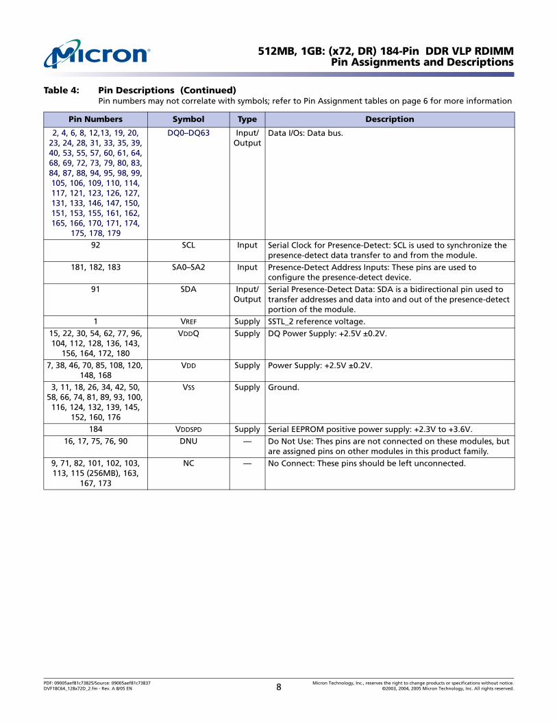
512MB, 1GB: (x72, DR) 184-Pin DDR VLP RDIMMPin Assignments and Descriptions
2, 4, 6, 8, 12,13, 19, 20, 23, 24, 28, 31, 33, 35, 39, 40, 53, 55, 57, 60, 61, 64, 68, 69, 72, 73, 79, 80, 83, 84, 87, 88, 94, 95, 98, 99, 105, 106, 109, 110, 114, 117, 121, 123, 126, 127, 131, 133, 146, 147, 150, 151, 153, 155, 161, 162, 165, 166, 170, 171, 174,
175, 178, 179
DQ0–DQ63 Input/Output
Data I/Os: Data bus.
92 SCL Input Serial Clock for Presence-Detect: SCL is used to synchronize the presence-detect data transfer to and from the module.
181, 182, 183 SA0–SA2 Input Presence-Detect Address Inputs: These pins are used to configure the presence-detect device.
91 SDA Input/Output
Serial Presence-Detect Data: SDA is a bidirectional pin used to transfer addresses and data into and out of the presence-detect portion of the module.
1 VREF Supply SSTL_2 reference voltage.15, 22, 30, 54, 62, 77, 96, 104, 112, 128, 136, 143,
156, 164, 172, 180
VDDQ Supply DQ Power Supply: +2.5V ±0.2V.
7, 38, 46, 70, 85, 108, 120, 148, 168
VDD Supply Power Supply: +2.5V ±0.2V.
3, 11, 18, 26, 34, 42, 50, 58, 66, 74, 81, 89, 93, 100, 116, 124, 132, 139, 145,
152, 160, 176
VSS Supply Ground.
184 VDDSPD Supply Serial EEPROM positive power supply: +2.3V to +3.6V.16, 17, 75, 76, 90 DNU — Do Not Use: Thes pins are not connected on these modules, but
are assigned pins on other modules in this product family.9, 71, 82, 101, 102, 103, 113, 115 (256MB), 163,
167, 173
NC — No Connect: These pins should be left unconnected.
Table 4: Pin Descriptions (Continued)Pin numbers may not correlate with symbols; refer to Pin Assignment tables on page 6 for more information
Pin Numbers Symbol Type Description
PDF: 09005aef81c73825/Source: 09005aef81c73837 Micron Technology, Inc., reserves the right to change products or specifications without notice.DVF18C64_128x72D_2.fm - Rev. A 8/05 EN 8 ©2003, 2004, 2005 Micron Technology, Inc. All rights reserved.
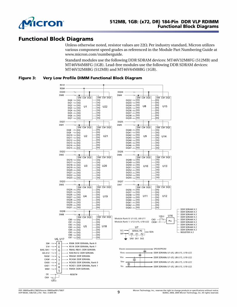
512MB, 1GB: (x72, DR) 184-Pin DDR VLP RDIMMFunctional Block Diagrams
Functional Block DiagramsUnless otherwise noted, resistor values are 22Ω. Per industry standard, Micron utilizes various component speed grades as referenced in the Module Part Numbering Guide at www.micron.com/numberguide.
Standard modules use the following DDR SDRAM devices: MT46V32M8FG (512MB) and MT46V64M8FG (1GB). Lead-free modules use the following DDR SDRAM devices: MT46V32M8BG (512MB) and MT46V64M8BG (1GB).
Figure 3: Very Low Profile DIMM Functional Block Diagram
A0
SA0
SERIAL PD SDAA1
SA1
A2
SA2
S0#
S1#
BA0, BA1
A0-A12
RAS#
CAS#
CKE0
CKE1
WE#
RS0#: DDR SDRAMs, Rank 0
RS1#: DDR SDRAMs, Rank 1
RBA0, RBA1: DDR SDRAMs
RA0-RA12: DDR SDRAMs
RRAS#: DDR SDRAMs
RCAS#: DDR SDRAMs
RCKE0: DDR SDRAMs, Rank 0
RCKE1: DDR SDRAMs, Rank 1
RWE#: DDR SDRAMs
CK
CK#
VREF
VSS
DDR SDRAMs U1-U5, U8-U15, U18-U22
DDR SDRAMs U1-U5, U8-U15, U18-U22
DQ56DQ57DQ58DQ59DQ60DQ61DQ62DQ63
U11
DQ48DQ49DQ50DQ51DQ52DQ53DQ54DQ55
U9
DQ40DQ41DQ42DQ43DQ44DQ45DQ46DQ47
U8
DQ32DQ33DQ34DQ35DQ36DQ37DQ38DQ39
DQ24DQ25DQ26DQ27DQ28DQ29DQ30DQ31
U4
DQ16DQ17DQ18DQ19DQ20DQ21DQ22DQ23
U2
DQ8DQ9DQ10DQ11DQ12DQ13DQ14DQ15
DM CS# DQSDQDQDQDQDQDQDQDQ
DQ0DQ1DQ2DQ3DQ4DQ5DQ6DQ7
DM0
RS0#
REGISTERS
WP
PLL
DDR SDRAM X 2DDR SDRAM X 2DDR SDRAM X 2DDR SDRAM X 2DDR SDRAM X 2DDR SDRAM X 2DDR SDRAM X 2DDR SDRAM X 2DDR SDRAM X 2REGISTER X 2
SCL
U1
U21
U3
U15
RS1#
DM CS# DQS
DM CS# DQS DM CS# DQS
DM CS# DQS DM CS# DQS
DM CS# DQS
DQS0
DM4
DQS4
DM1
DQS1
DM5
DQS5
U14
DM CS# DQS
DM2
DQS2
DM6
DQS6
DM CS# DQS DM CS# DQS
U10 U13
DM CS# DQS DM CS# DQS
DM CS# DQS DM CS# DQS
DM CS# DQS
DM3
DQS3
DM7DQS7
U19
DM CS# DQS
U12
DM8
DQS8
U5
DM CS# DQSCB0CB1CB2CB3CB4CB5CB6CB7
VDDQ
VDD DDR SDRAMs U1-U5, U8-U15, U18-U22
DDR SDRAMs U1-U5, U8-U15, U18-U22
CK0CK0#
120
U6, U17
U7
U16
DQDQDQDQDQDQDQDQ
DQDQDQDQDQDQDQDQ
DQDQDQDQDQDQDQDQ
DQDQDQDQDQDQDQDQ
DQDQDQDQDQDQDQDQ
DQDQDQDQDQDQDQDQ
DQDQDQDQDQDQDQDQ
DQDQDQDQDQDQDQDQ
DQDQDQDQDQDQDQDQ
DQDQDQDQDQDQDQDQ
DQDQDQDQDQDQDQDQ
DQDQDQDQDQDQDQDQ
DQDQDQDQDQDQDQDQ
DQDQDQDQDQDQDQDQ
DQDQDQDQDQDQDQDQ
DQDQDQDQDQDQDQDQ
DQDQDQDQDQDQDQDQ
U22
U20
U18
Module Rank 0: U1-U5, U8-U11
Module Rank 1: U12-U15, U18-U22
120
DM CS# DQS
VDDSPD SPD/EEPROM
RESET#
PDF: 09005aef81c73825/Source: 09005aef81c73837 Micron Technology, Inc., reserves the right to change products or specifications without notice.DVF18C64_128x72D_2.fm - Rev. A 8/05 EN 9 ©2003, 2004, 2005 Micron Technology, Inc. All rights reserved.
512MB, 1GB: (x72, DR) 184-Pin DDR VLP RDIMMGeneral Description
General DescriptionThe MT18VDVF6472D and MT18VDVF12872D are high-speed CMOS, dynamic random-access, 512MB and 1GB memory modules organized in x72 (ECC) configuration. DDR SDRAM modules use internally configured quad-bank DDR SDRAM devices.
DDR SDRAM modules use a double data rate architecture to achieve high-speed opera-tion. Double data rate architecture is essentially a 2n-prefetch architecture with an interface designed to transfer two data words per clock cycle at the I/O pins. A single read or write access for the DDR SDRAM module effectively consists of a single 2n-bit wide, one-clock-cycle data transfer at the internal DRAM core and two corresponding n-bit wide, one-half-clock-cycle data transfers at the I/O pins.
A bidirectional data strobe (DQS) is transmitted externally, along with data, for use in data capture at the receiver. DQS is an intermittent strobe transmitted by the DDR SDRAM during READs and by the memory controller during WRITEs. DQS is edge-aligned with data for READs and center-aligned with data for WRITEs.
DDR SDRAM modules operate from differential clock inputs (CK and CK#); the crossing of CK going HIGH and CK# going LOW will be referred to as the positive edge of CK. Commands (address and control signals) are registered at every positive edge of CK. Input data is registered on both edges of DQS, and output data is referenced to both edges of DQS, as well as to both edges of CK.
Read and write accesses to DDR SDRAM modules are burst oriented; accesses start at a selected location and continue for a programmed number of locations in a programmed sequence. Accesses begin with the registration of an ACTIVE command, which is then followed by a READ or WRITE command. The address bits registered coincident with the ACTIVE command are used to select the device bank and row to be accessed (BA0, BA1 select devices bank; A0–A12 select device row). The address bits registered coinci-dent with the READ or WRITE command are used to select the device bank and starting device column location for the burst access.
DDR SDRAM modules provide for programmable READ or WRITE burst lengths of 2, 4, or 8 locations. An auto precharge function may be enabled to provide a self-timed row precharge that is initiated at the end of the burst access.
The pipelined, multibank architecture of DDR SDRAM modules allows for concurrent operation, thereby providing high effective bandwidth by hiding row precharge and acti-vation time.
An auto refresh mode is provided, along with a power-saving power-down mode. All inputs are compatible with the JEDEC Standard for SSTL_2. All outputs are SSTL_2, Class II compatible. For more information regarding DDR SDRAM operation, refer to the 256Mb or 512Mb DDR SDRAM component data sheets.
PLL and Register OperationDDR SDRAM modules operate in registered mode, where the command/address input signals are latched in the registers on the rising clock edge and sent to the DDR SDRAM devices on the following rising clock edge (data access is delayed by one clock cycle). A phase-lock loop (PLL) on the module receives and redrives the differential clock signals (CK, CK#) to the DDR SDRAM devices. The registers and PLL minimize system and clock loading.
Serial Presence-Detect OperationDDR SDRAM modules incorporate serial presence-detect (SPD). The SPD function is implemented using a 2,048-bit EEPROM. This nonvolatile storage device contains 256 bytes. The first 128 bytes can be programmed by Micron to identify the module type and
PDF: 09005aef81c73825/Source: 09005aef81c73837 Micron Technology, Inc., reserves the right to change products or specifications without notice.DVF18C64_128x72D_2.fm - Rev. A 8/05 EN 10 ©2003, 2004, 2005 Micron Technology, Inc. All rights reserved.
512MB, 1GB: (x72, DR) 184-Pin DDR VLP RDIMMMode Register Definition
various SDRAM organizations and timing parameters. The remaining 128 bytes of stor-age are available for use by the customer. System READ/WRITE operations between the master (system logic) and the slave EEPROM device (DIMM) occur via a standard I2C bus using the DIMM’s SCL (clock) and SDA (data) signals, together with SA (2:0), which provide eight unique DIMM/EEPROM addresses. Write protect (WP) is tied to ground on the module, permanently disabling hardware write protect.
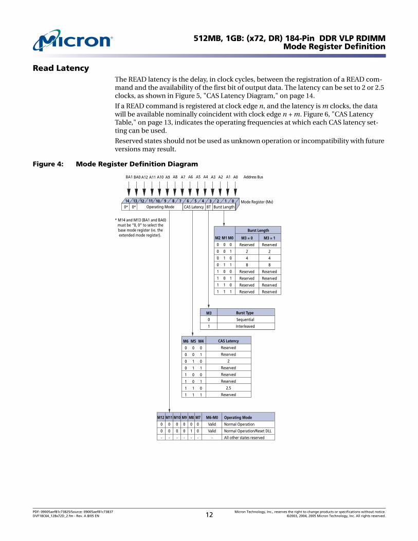
Mode Register DefinitionThe mode register is used to define the specific mode of operation of DDR SDRAM devices. This definition includes the selection of a burst length, a burst type, a CAS latency and an operating mode, as shown in Figure 4, "Mode Register Definition Dia-gram," on page 12. The mode register is programmed via the MODE REGISTER SET command (with BA0 = 0 and BA1 = 0) and will retain the stored information until it is programmed again or the device loses power (except for bit A8, which is self-clearing).
Reprogramming the mode register will not alter the contents of the memory, provided it is performed correctly. The mode register must be loaded (reloaded) when all device banks are idle and no bursts are in progress, and the controller must wait the specified time before initiating the subsequent operation. Violating either of these requirements will result in unspecified operation.
Mode register bits A0–A2 specify the burst length, A3 specifies the type of burst (sequen-tial or interleaved), A4–A6 specify the CAS latency, and A7–A12 specify the operating mode.
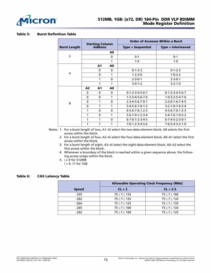
Burst LengthRead and write accesses to DDR SDRAM devices are burst oriented, with the burst length being programmable, as shown in Figure 4, "Mode Register Definition Diagram," on page 12. The burst length determines the maximum number of column locations that can be accessed for a given READ or WRITE command. Burst lengths of 2, 4, or 8 locations are available for both the sequential and the interleaved burst types.
Reserved states should not be used, as unknown operation or incompatibility with future versions may result.
When a READ or WRITE command is issued, a block of columns equal to the burst length is effectively selected. All accesses for that burst take place within this block, meaning that the burst will wrap within the block if a boundary is reached. The block is uniquely selected by A1–Ai when the burst length is set to two, by A2–Ai when the burst length is set to four and by A3–Ai when the burst length is set to eight (where Ai is the most significant column address bit for a given configuration. See Note 5 of Table 5, "Burst Definition Table," on page 13, for Ai values). The remaining (least significant) address bit(s) is (are) used to select the starting location within the block. The pro-grammed burst length applies to both READ and WRITE bursts.
Burst TypeAccesses within a given burst may be programmed to be either sequential or interleaved; this is referred to as the burst type and is selected via bit M3.
The ordering of accesses within a burst is determined by the burst length, the burst type and the starting column address, as shown in Table 5, "Burst Definition Table," on page 13.
PDF: 09005aef81c73825/Source: 09005aef81c73837 Micron Technology, Inc., reserves the right to change products or specifications without notice.DVF18C64_128x72D_2.fm - Rev. A 8/05 EN 11 ©2003, 2004, 2005 Micron Technology, Inc. All rights reserved.
512MB, 1GB: (x72, DR) 184-Pin DDR VLP RDIMMMode Register Definition
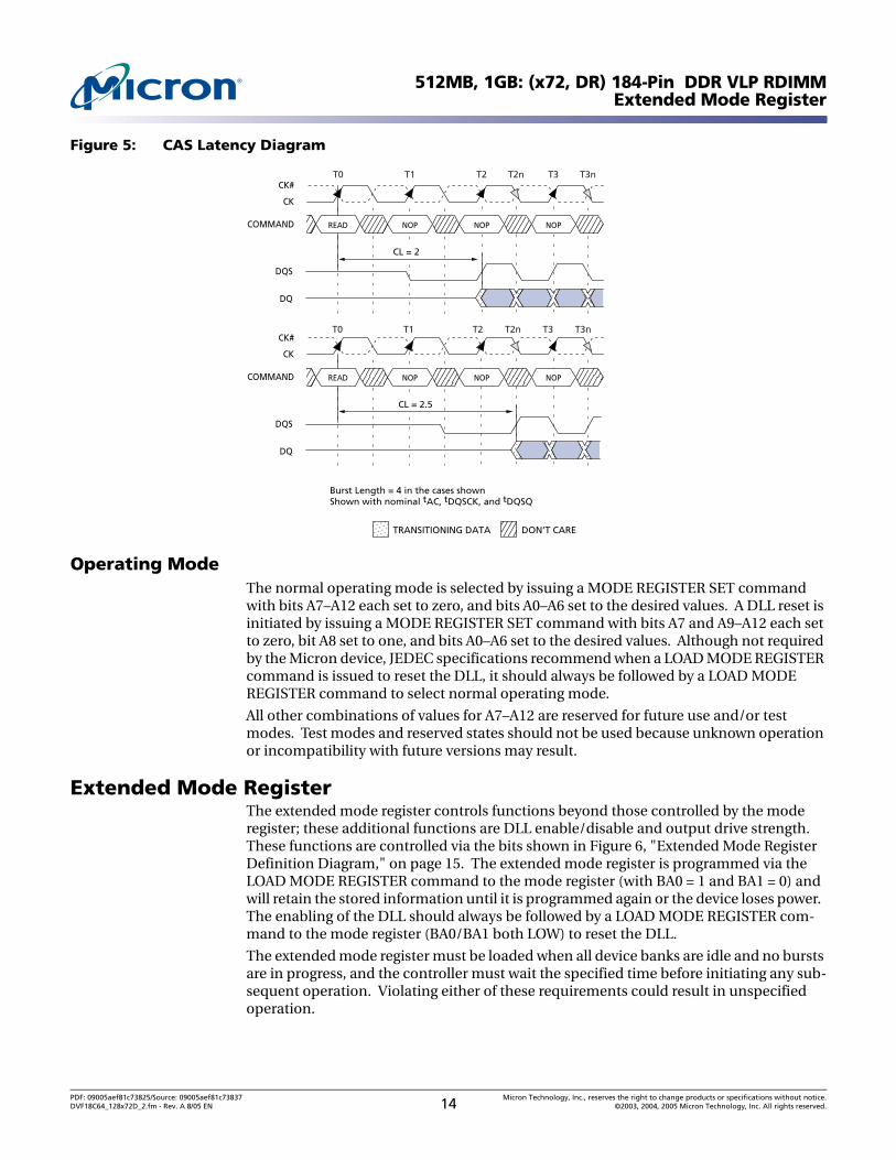
Read LatencyThe READ latency is the delay, in clock cycles, between the registration of a READ com-mand and the availability of the first bit of output data. The latency can be set to 2 or 2.5 clocks, as shown in Figure 5, "CAS Latency Diagram," on page 14.
If a READ command is registered at clock edge n, and the latency is m clocks, the data will be available nominally coincident with clock edge n + m. Figure 6, "CAS Latency Table," on page 13, indicates the operating frequencies at which each CAS latency set-ting can be used.
Reserved states should not be used as unknown operation or incompatibility with future versions may result.
Figure 4: Mode Register Definition Diagram
M3 = 0
Reserved
2
4
8
Reserved
Reserved
Reserved
Reserved
M3 = 1
Reserved
2
4
8
Reserved
Reserved
Reserved
Reserved
Operating Mode
Normal Operation
Normal Operation/Reset DLL
All other states reserved
0
1
-
0
0
-
0
0
-
0
0
-
0
0
-
0
0
-
Valid
Valid
-
0
1
Burst Type
Sequential
Interleaved
CAS Latency
Reserved
Reserved
2
Reserved
Reserved
Reserved
2.5
Reserved
Burst Length
M0
0
1
0
1
0
1
0
1
Burst LengthCAS Latency BT0*
A9 A7 A6 A5 A4 A3A8 A2 A1 A0
Mode Register (Mx)
Address Bus
9 7 6 5 4 38 2 1 0
M1
0
0
1
1
0
0
1
1
M2
0
0
0
0
1
1
1
1
M3
M4
0
1
0
1
0
1
0
1
M5
0
0
1
1
0
0
1
1
M6
0
0
0
0
1
1
1
1
M6-M0M8 M7
Operating Mode
A10A12 A11BA0BA1
101112130*14
* M14 and M13 (BA1 and BA0)must be “0, 0” to select thebase mode register (vs. theextended mode register).
M9M10M12 M11
PDF: 09005aef81c73825/Source: 09005aef81c73837 Micron Technology, Inc., reserves the right to change products or specifications without notice.DVF18C64_128x72D_2.fm - Rev. A 8/05 EN 12 ©2003, 2004, 2005 Micron Technology, Inc. All rights reserved.
512MB, 1GB: (x72, DR) 184-Pin DDR VLP RDIMMMode Register Definition
Notes: 1. For a burst length of two, A1–Ai select the two-data-element block; A0 selects the first access within the block.
2. For a burst length of four, A2–Ai select the four-data-element block; A0–A1 select the first access within the block.
3. For a burst length of eight, A3–Ai select the eight-data-element block; A0–A2 select the first access within the block.
4. Whenever a boundary of the block is reached within a given sequence above, the follow-ing access wraps within the block.
5. i = 9 for 512MBi = 9, 11 for 1GB
Table 5: Burst Definition Table
Burst LengthStarting Column
Address
Order of Accesses Within a Burst
Type = Sequential Type = Interleaved
2A00 0-1 0-11 1-0 1-0
4
A1 A00 0 0-1-2-3 0-1-2-30 1 1-2-3-0 1-0-3-21 0 2-3-0-1 2-3-0-11 1 3-0-1-2 3-2-1-0
8
A2 A1 A00 0 0 0-1-2-3-4-5-6-7 0-1-2-3-4-5-6-70 0 1 1-2-3-4-5-6-7-0 1-0-3-2-5-4-7-60 1 0 2-3-4-5-6-7-0-1 2-3-0-1-6-7-4-50 1 1 3-4-5-6-7-0-1-2 3-2-1-0-7-6-5-41 0 0 4-5-6-7-0-1-2-3 4-5-6-7-0-1-2-31 0 1 5-6-7-0-1-2-3-4 5-4-7-6-1-0-3-21 1 0 6-7-0-1-2-3-4-5 6-7-4-5-2-3-0-11 1 1 7-0-1-2-3-4-5-6 7-6-5-4-3-2-1-0
Table 6: CAS Latency Table
Speed
Allowable Operating Clock Frequency (MHz)
CL = 2 CL = 2.5
-335 75 ≤ f ≤ 133 75 ≤ f ≤ 166-262 75 ≤ f ≤ 133 75 ≤ f ≤ 133-26A 75 ≤ f ≤ 133 75 ≤ f ≤ 133-265 75 ≤ f ≤ 100 75 ≤ f ≤ 133-202 75 ≤ f ≤ 100 75 ≤ f ≤ 125
PDF: 09005aef81c73825/Source: 09005aef81c73837 Micron Technology, Inc., reserves the right to change products or specifications without notice.DVF18C64_128x72D_2.fm - Rev. A 8/05 EN 13 ©2003, 2004, 2005 Micron Technology, Inc. All rights reserved.
512MB, 1GB: (x72, DR) 184-Pin DDR VLP RDIMMExtended Mode Register
Figure 5: CAS Latency Diagram
Operating ModeThe normal operating mode is selected by issuing a MODE REGISTER SET command with bits A7–A12 each set to zero, and bits A0–A6 set to the desired values. A DLL reset is initiated by issuing a MODE REGISTER SET command with bits A7 and A9–A12 each set to zero, bit A8 set to one, and bits A0–A6 set to the desired values. Although not required by the Micron device, JEDEC specifications recommend when a LOAD MODE REGISTER command is issued to reset the DLL, it should always be followed by a LOAD MODE REGISTER command to select normal operating mode.
All other combinations of values for A7–A12 are reserved for future use and/or test modes. Test modes and reserved states should not be used because unknown operation or incompatibility with future versions may result.
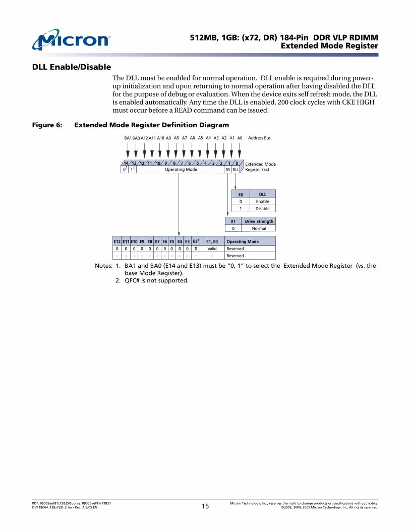
Extended Mode RegisterThe extended mode register controls functions beyond those controlled by the mode register; these additional functions are DLL enable/disable and output drive strength. These functions are controlled via the bits shown in Figure 6, "Extended Mode Register Definition Diagram," on page 15. The extended mode register is programmed via the LOAD MODE REGISTER command to the mode register (with BA0 = 1 and BA1 = 0) and will retain the stored information until it is programmed again or the device loses power. The enabling of the DLL should always be followed by a LOAD MODE REGISTER com-mand to the mode register (BA0/BA1 both LOW) to reset the DLL.
The extended mode register must be loaded when all device banks are idle and no bursts are in progress, and the controller must wait the specified time before initiating any sub-sequent operation. Violating either of these requirements could result in unspecified operation.
CK
CK#
COMMAND
DQ
DQS
CL = 2
READ NOP NOP NOP
READ NOP NOP NOP
Burst Length = 4 in the cases shownShown with nominal tAC, tDQSCK, and tDQSQ
CK
CK#
COMMAND
DQ
DQS
CL = 2.5
T0 T1 T2 T2n T3 T3n
T0 T1 T2 T2n T3 T3n
DON’T CARETRANSITIONING DATA
PDF: 09005aef81c73825/Source: 09005aef81c73837 Micron Technology, Inc., reserves the right to change products or specifications without notice.DVF18C64_128x72D_2.fm - Rev. A 8/05 EN 14 ©2003, 2004, 2005 Micron Technology, Inc. All rights reserved.
512MB, 1GB: (x72, DR) 184-Pin DDR VLP RDIMMExtended Mode Register
DLL Enable/DisableThe DLL must be enabled for normal operation. DLL enable is required during power-up initialization and upon returning to normal operation after having disabled the DLL for the purpose of debug or evaluation. When the device exits self refresh mode, the DLL is enabled automatically. Any time the DLL is enabled, 200 clock cycles with CKE HIGH must occur before a READ command can be issued.
Figure 6: Extended Mode Register Definition Diagram
Notes: 1. BA1 and BA0 (E14 and E13) must be “0, 1” to select the Extended Mode Register (vs. the base Mode Register).
2. QFC# is not supported.
Operating Mode
Reserved
Reserved
0
–
0
–
Valid
–
0
1
DLL
Enable
Disable
DLL1101
A9 A7 A6 A5 A4 A3A8 A2 A1 A0
Extended ModeRegister (Ex)
Address Bus
9 7 6 5 4 38 2 1 0
E0
0
Drive Strength
Normal
E1
E0E1,
Operating Mode
A10A11A12BA1 BA0
1011121314
E3E4
0
–
0
–
0
–
0
–
0
–
E6 E5E7E8E9
0
–
0
–
E10E11
0
–
E12
DS
0
–
E22
PDF: 09005aef81c73825/Source: 09005aef81c73837 Micron Technology, Inc., reserves the right to change products or specifications without notice.DVF18C64_128x72D_2.fm - Rev. A 8/05 EN 15 ©2003, 2004, 2005 Micron Technology, Inc. All rights reserved.
512MB, 1GB: (x72, DR) 184-Pin DDR VLP RDIMMCommands
CommandsTable 7, Commands Truth Table, and Table 8, DM Operation Truth Table, provide a gen-eral reference of available commands. For a more detailed description of commands and operations, refer to the 256Mb or 512Mb DDR SDRAM component data sheets.
Notes: 1. DESELECT and NOP are functionally interchangeable.2. BA0–BA1 provide device bank address and A0–A12 provide row address.3. BA0–BA1 provide device bank address; A0–A9 (512MB) or A0–A9, A11 (1GB) provide col-
umn address; A10 HIGH enables the auto precharge feature (nonpersistent), and A10 LOW disables the auto precharge feature.
4. Applies only to read bursts with auto precharge disabled; this command is undefined (and should not be used) for READ bursts with auto precharge enabled and for WRITE bursts.
5. A10 LOW: BA0–BA1 determine which device bank is precharged. A10 HIGH: all device banks are precharged and BA0–BA1 are “Don’t Care.”
6. This command is AUTO REFRESH if CKE is HIGH, SELF REFRESH if CKE is LOW.7. Internal refresh counter controls row addressing; all inputs and I/Os are “Don’t Care”
except for CKE.8. BA0-BA1 select either the mode register or the extended mode register (BA0 = 0, BA1 = 0
select the mode register; BA0 = 1, BA1 = 0 select extended mode register; other combina-tions of BA0–BA1 are reserved). A0–A12 provide the op-code to be written to the selected mode register.
Table 7: Commands Truth TableCKE is HIGH for all commands shown except SELF REFRESH; all states and sequences not shown are illegal or reserved
NAME (FUNCTION) CS# RAS# CAS# WE# ADDR NOTES
DESELECT (NOP) H X X X X 1
NO OPERATION (NOP) L H H H X 1
ACTIVE (Select bank and activate row) L L H H Bank/Row 2
READ (Select bank and column, and start READ burst) L H L H Bank/Col 3
WRITE (Select bank and column, and start WRITE burst) L H L L Bank/Col 3
BURST TERMINATE L H H L X 4
PRECHARGE (Deactivate row in bank or banks) L L H L Code 5
AUTO REFRESH or SELF REFRESH(Enter self refresh mode)
L L L H X 6, 7
LOAD MODE REGISTER L L L L Op-Code 8
Table 8: DM Operation Truth TableUsed to mask write data; provided coincident with the corresponding data
NAME (FUNCTION) DM DQs
WRITE Enable L Valid
WRITE Inhibit H X
PDF: 09005aef81c73825/Source: 09005aef81c73837 Micron Technology, Inc., reserves the right to change products or specifications without notice.DVF18C64_128x72D_2.fm - Rev. A 8/05 EN 16 ©2003, 2004, 2005 Micron Technology, Inc. All rights reserved.
512MB, 1GB: (x72, DR) 184-Pin DDR VLP RDIMMAbsolute Maximum Ratings
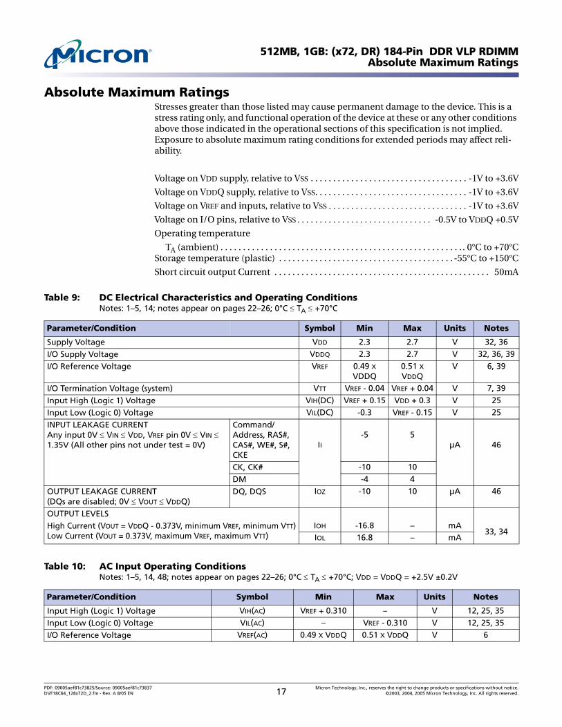
Absolute Maximum RatingsStresses greater than those listed may cause permanent damage to the device. This is a stress rating only, and functional operation of the device at these or any other conditions above those indicated in the operational sections of this specification is not implied. Exposure to absolute maximum rating conditions for extended periods may affect reli-ability.
Voltage on VDD supply, relative to VSS . . . . . . . . . . . . . . . . . . . . . . . . . . . . . . . . . . . -1V to +3.6V
Voltage on VDDQ supply, relative to VSS. . . . . . . . . . . . . . . . . . . . . . . . . . . . . . . . . . -1V to +3.6V
Voltage on VREF and inputs, relative to VSS . . . . . . . . . . . . . . . . . . . . . . . . . . . . . . . -1V to +3.6V
Voltage on I/O pins, relative to VSS . . . . . . . . . . . . . . . . . . . . . . . . . . . . . . -0.5V to VDDQ +0.5V
Operating temperature
TA (ambient) . . . . . . . . . . . . . . . . . . . . . . . . . . . . . . . . . . . . . . . . . . . . . . . . . . . . . . . 0°C to +70°CStorage temperature (plastic) . . . . . . . . . . . . . . . . . . . . . . . . . . . . . . . . . . . . . . . -55°C to +150°C
Short circuit output Current . . . . . . . . . . . . . . . . . . . . . . . . . . . . . . . . . . . . . . . . . . . . . . . . 50mA
Table 9: DC Electrical Characteristics and Operating ConditionsNotes: 1–5, 14; notes appear on pages 22–26; 0°C ≤ TA ≤ +70°C
Parameter/Condition Symbol Min Max Units Notes
Supply Voltage VDD 2.3 2.7 V 32, 36
I/O Supply Voltage VDDQ 2.3 2.7 V 32, 36, 39
I/O Reference Voltage VREF 0.49 X VDDQ
0.51 X VDDQ
V 6, 39
I/O Termination Voltage (system) VTT VREF - 0.04 VREF + 0.04 V 7, 39
Input High (Logic 1) Voltage VIH(DC) VREF + 0.15 VDD + 0.3 V 25
Input Low (Logic 0) Voltage VIL(DC) -0.3 VREF - 0.15 V 25
INPUT LEAKAGE CURRENTAny input 0V ≤ VIN ≤ VDD, VREF pin 0V ≤ VIN ≤ 1.35V (All other pins not under test = 0V)
Command/Address, RAS#, CAS#, WE#, S#, CKE
II-5 5
µA 46
CK, CK# -10 10
DM -4 4
OUTPUT LEAKAGE CURRENT(DQs are disabled; 0V ≤ VOUT ≤ VDDQ)
DQ, DQS IOZ -10 10 µA 46
OUTPUT LEVELSHigh Current (VOUT = VDDQ - 0.373V, minimum VREF, minimum VTT)Low Current (VOUT = 0.373V, maximum VREF, maximum VTT)
IOH -16.8 – mA33, 34
IOL 16.8 – mA
Table 10: AC Input Operating ConditionsNotes: 1–5, 14, 48; notes appear on pages 22–26; 0°C ≤ TA ≤ +70°C; VDD = VDDQ = +2.5V ±0.2V
Parameter/Condition Symbol Min Max Units Notes
Input High (Logic 1) Voltage VIH(AC) VREF + 0.310 – V 12, 25, 35
Input Low (Logic 0) Voltage VIL(AC) – VREF - 0.310 V 12, 25, 35
I/O Reference Voltage VREF(AC) 0.49 X VDDQ 0.51 X VDDQ V 6
PDF: 09005aef81c73825/Source: 09005aef81c73837 Micron Technology, Inc., reserves the right to change products or specifications without notice.DVF18C64_128x72D_2.fm - Rev. A 8/05 EN 17 ©2003, 2004, 2005 Micron Technology, Inc. All rights reserved.
512MB, 1GB: (x72, DR) 184-Pin DDR VLP RDIMMElectrical Specifications
Electrical Specifications
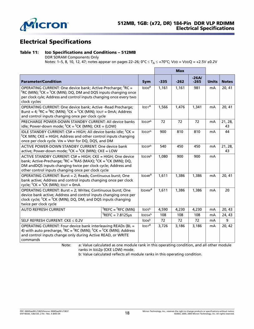
Table 11: IDD Specifications and Conditions – 512MBDDR SDRAM Components OnlyNotes: 1–5, 8, 10, 12, 47; notes appear on pages 22–26; 0°C ≤ TA ≤ +70°C; VDD = VDDQ = +2.5V ±0.2V
Max
Parameter/Condition Sym -335 -262-26A/-265 Units Notes
OPERATING CURRENT: One device bank; Active-Precharge; tRC = tRC (MIN); tCK = tCK (MIN); DQ, DM and DQS inputs changing once per clock cyle; Address and control inputs changing once every two clock cycles
IDD0a 1,161 1,161 981 mA 20, 41
OPERATING CURRENT: One device bank; Active -Read Precharge; Burst = 4; tRC = tRC (MIN); tCK = tCK (MIN); IOUT = 0mA; Address and control inputs changing once per clock cycle
IDD1a 1,566 1,476 1,341 mA 20, 41
PRECHARGE POWER-DOWN STANDBY CURRENT: All device banks idle; Power-down mode; tCK = tCK (MIN); CKE = (LOW)
IDD2Pb 72 72 72 mA 21, 28, 43
IDLE STANDBY CURRENT: CS# = HIGH; All device banks idle; tCK = tCK MIN; CKE = HIGH; Address and other control inputs changing once per clock cycle. VIN = VREF for DQ, DQS, and DM
IDD2Fb 900 810 810 mA 44
ACTIVE POWER-DOWN STANDBY CURRENT: One device bank active; Power-down mode; tCK = tCK (MIN); CKE = LOW
IDD3Pb 540 450 450 mA 21, 28, 43
ACTIVE STANDBY CURRENT: CS# = HIGH; CKE = HIGH; One device bank; Active-Precharge; tRC = tRAS (MAX); tCK = tCK (MIN); DQ, DM andDQS inputs changing twice per clock cycle; Address and other control inputs changing once per clock cycle
IDD3Nb 1,080 900 900 mA
OPERATING CURRENT: Burst = 2; Reads; Continuous burst; One bank active; Address and control inputs changing once per clock cycle; tCK = tCK (MIN); IOUT = 0mA
IDD4Ra 1,611 1,386 1,386 mA 20, 41
OPERATING CURRENT: Burst = 2; Writes; Continuous burst; One device bank active; Address and control inputs changing once per clock cycle; tCK = tCK (MIN); DQ, DM, and DQS inputs changing twice per clock cycle
IDD4Wa 1,611 1,386 1,386 mA 20
AUTO REFRESH CURRENT tREFC = tRFC (MIN) IDD5b 4,590 4,230 4,230 mA 20, 43tREFC = 7.8125µs IDD5Ab 108 108 108 mA 24, 43
SELF REFRESH CURRENT: CKE ≤ 0.2V IDD6b 72 72 72 mA 9
OPERATING CURRENT: Four device bank interleaving READs (BL = 4) with auto precharge, tRC = tRC (MIN); tCK = tCK (MIN); Address and control inputs change only during Active READ, or WRITE commands
IDD7a 3,726 3,186 3,186 mA 20, 42
Note: a: Value calculated as one module rank in this operating condition, and all other module ranks in IDD2p (CKE LOW) mode.b: Value calculated reflects all module ranks in this operating condition.
PDF: 09005aef81c73825/Source: 09005aef81c73837 Micron Technology, Inc., reserves the right to change products or specifications without notice.DVF18C64_128x72D_2.fm - Rev. A 8/05 EN 18 ©2003, 2004, 2005 Micron Technology, Inc. All rights reserved.
512MB, 1GB: (x72, DR) 184-Pin DDR VLP RDIMMElectrical Specifications
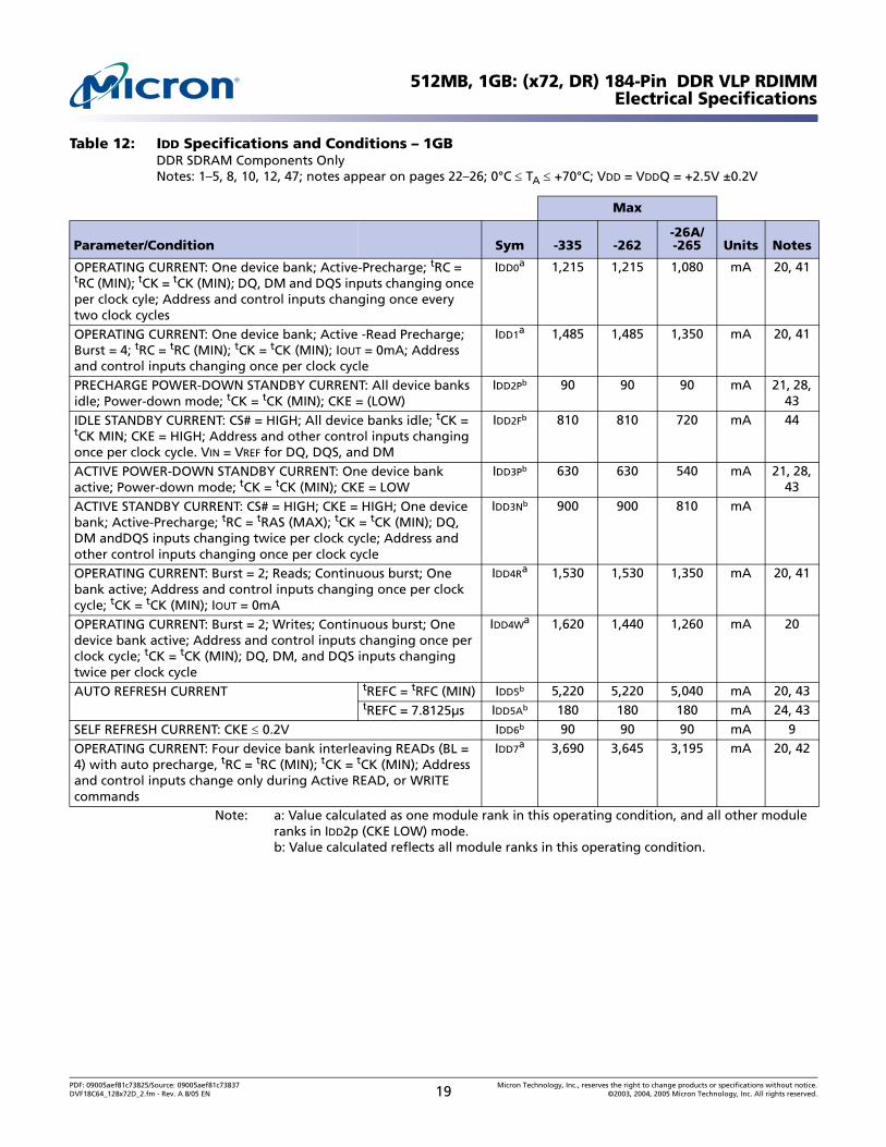
Table 12: IDD Specifications and Conditions – 1GBDDR SDRAM Components OnlyNotes: 1–5, 8, 10, 12, 47; notes appear on pages 22–26; 0°C ≤ TA ≤ +70°C; VDD = VDDQ = +2.5V ±0.2V
Max
Parameter/Condition Sym -335 -262-26A/-265 Units Notes
OPERATING CURRENT: One device bank; Active-Precharge; tRC = tRC (MIN); tCK = tCK (MIN); DQ, DM and DQS inputs changing once per clock cyle; Address and control inputs changing once every two clock cycles
IDD0a 1,215 1,215 1,080 mA 20, 41
OPERATING CURRENT: One device bank; Active -Read Precharge; Burst = 4; tRC = tRC (MIN); tCK = tCK (MIN); IOUT = 0mA; Address and control inputs changing once per clock cycle
IDD1a 1,485 1,485 1,350 mA 20, 41
PRECHARGE POWER-DOWN STANDBY CURRENT: All device banks idle; Power-down mode; tCK = tCK (MIN); CKE = (LOW)
IDD2Pb 90 90 90 mA 21, 28, 43
IDLE STANDBY CURRENT: CS# = HIGH; All device banks idle; tCK = tCK MIN; CKE = HIGH; Address and other control inputs changing once per clock cycle. VIN = VREF for DQ, DQS, and DM
IDD2Fb 810 810 720 mA 44
ACTIVE POWER-DOWN STANDBY CURRENT: One device bank active; Power-down mode; tCK = tCK (MIN); CKE = LOW
IDD3Pb 630 630 540 mA 21, 28, 43
ACTIVE STANDBY CURRENT: CS# = HIGH; CKE = HIGH; One device bank; Active-Precharge; tRC = tRAS (MAX); tCK = tCK (MIN); DQ, DM andDQS inputs changing twice per clock cycle; Address and other control inputs changing once per clock cycle
IDD3Nb 900 900 810 mA
OPERATING CURRENT: Burst = 2; Reads; Continuous burst; One bank active; Address and control inputs changing once per clock cycle; tCK = tCK (MIN); IOUT = 0mA
IDD4Ra 1,530 1,530 1,350 mA 20, 41
OPERATING CURRENT: Burst = 2; Writes; Continuous burst; One device bank active; Address and control inputs changing once per clock cycle; tCK = tCK (MIN); DQ, DM, and DQS inputs changing twice per clock cycle
IDD4Wa 1,620 1,440 1,260 mA 20
AUTO REFRESH CURRENT tREFC = tRFC (MIN) IDD5b 5,220 5,220 5,040 mA 20, 43tREFC = 7.8125µs IDD5Ab 180 180 180 mA 24, 43
SELF REFRESH CURRENT: CKE ≤ 0.2V IDD6b 90 90 90 mA 9
OPERATING CURRENT: Four device bank interleaving READs (BL = 4) with auto precharge, tRC = tRC (MIN); tCK = tCK (MIN); Address and control inputs change only during Active READ, or WRITE commands
IDD7a 3,690 3,645 3,195 mA 20, 42
Note: a: Value calculated as one module rank in this operating condition, and all other module ranks in IDD2p (CKE LOW) mode.b: Value calculated reflects all module ranks in this operating condition.
PDF: 09005aef81c73825/Source: 09005aef81c73837 Micron Technology, Inc., reserves the right to change products or specifications without notice.DVF18C64_128x72D_2.fm - Rev. A 8/05 EN 19 ©2003, 2004, 2005 Micron Technology, Inc. All rights reserved.
512MB, 1GB: (x72, DR) 184-Pin DDR VLP RDIMMElectrical Specifications
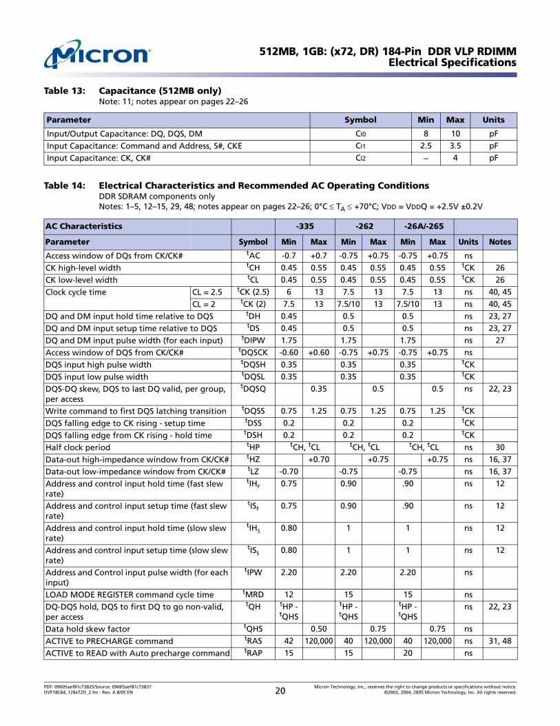
Table 13: Capacitance (512MB only)Note: 11; notes appear on pages 22–26
Parameter Symbol Min Max Units
Input/Output Capacitance: DQ, DQS, DM CI0 8 10 pF
Input Capacitance: Command and Address, S#, CKE CI1 2.5 3.5 pF
Input Capacitance: CK, CK# CI2 – 4 pF
Table 14: Electrical Characteristics and Recommended AC Operating ConditionsDDR SDRAM components onlyNotes: 1–5, 12–15, 29, 48; notes appear on pages 22–26; 0°C ≤ TA ≤ +70°C; VDD = VDDQ = +2.5V ±0.2V
AC Characteristics -335 -262 -26A/-265
Parameter Symbol Min Max Min Max Min Max Units Notes
Access window of DQs from CK/CK# tAC -0.7 +0.7 -0.75 +0.75 -0.75 +0.75 ns
CK high-level width tCH 0.45 0.55 0.45 0.55 0.45 0.55 tCK 26
CK low-level width tCL 0.45 0.55 0.45 0.55 0.45 0.55 tCK 26
Clock cycle time CL = 2.5 tCK (2.5) 6 13 7.5 13 7.5 13 ns 40, 45
CL = 2 tCK (2) 7.5 13 7.5/10 13 7.5/10 13 ns 40, 45
DQ and DM input hold time relative to DQS tDH 0.45 0.5 0.5 ns 23, 27
DQ and DM input setup time relative to DQS tDS 0.45 0.5 0.5 ns 23, 27
DQ and DM input pulse width (for each input) tDIPW 1.75 1.75 1.75 ns 27
Access window of DQS from CK/CK# tDQSCK -0.60 +0.60 -0.75 +0.75 -0.75 +0.75 ns
DQS input high pulse width tDQSH 0.35 0.35 0.35 tCK
DQS input low pulse width tDQSL 0.35 0.35 0.35 tCK
DQS-DQ skew, DQS to last DQ valid, per group, per access
tDQSQ 0.35 0.5 0.5 ns 22, 23
Write command to first DQS latching transition tDQSS 0.75 1.25 0.75 1.25 0.75 1.25 tCK
DQS falling edge to CK rising - setup time tDSS 0.2 0.2 0.2 tCK
DQS falling edge from CK rising - hold time tDSH 0.2 0.2 0.2 tCK
Half clock period tHP tCH, tCL tCH, tCL tCH, tCL ns 30
Data-out high-impedance window from CK/CK# tHZ +0.70 +0.75 +0.75 ns 16, 37
Data-out low-impedance window from CK/CK# tLZ -0.70 -0.75 -0.75 ns 16, 37
Address and control input hold time (fast slew rate)
tIHF 0.75 0.90 .90 ns 12
Address and control input setup time (fast slew rate)
tISF 0.75 0.90 .90 ns 12
Address and control input hold time (slow slew rate)
tIHS 0.80 1 1 ns 12
Address and control input setup time (slow slew rate)
tISS 0.80 1 1 ns 12
Address and Control input pulse width (for each input)
tIPW 2.20 2.20 2.20 ns
LOAD MODE REGISTER command cycle time tMRD 12 15 15 ns
DQ-DQS hold, DQS to first DQ to go non-valid, per access
tQH tHP - tQHS
tHP - tQHS
tHP - tQHS
ns 22, 23
Data hold skew factor tQHS 0.50 0.75 0.75 ns
ACTIVE to PRECHARGE command tRAS 42 120,000 40 120,000 40 120,000 ns 31, 48
ACTIVE to READ with Auto precharge command tRAP 15 15 20 ns
PDF: 09005aef81c73825/Source: 09005aef81c73837 Micron Technology, Inc., reserves the right to change products or specifications without notice.DVF18C64_128x72D_2.fm - Rev. A 8/05 EN 20 ©2003, 2004, 2005 Micron Technology, Inc. All rights reserved.
512MB, 1GB: (x72, DR) 184-Pin DDR VLP RDIMMElectrical Specifications
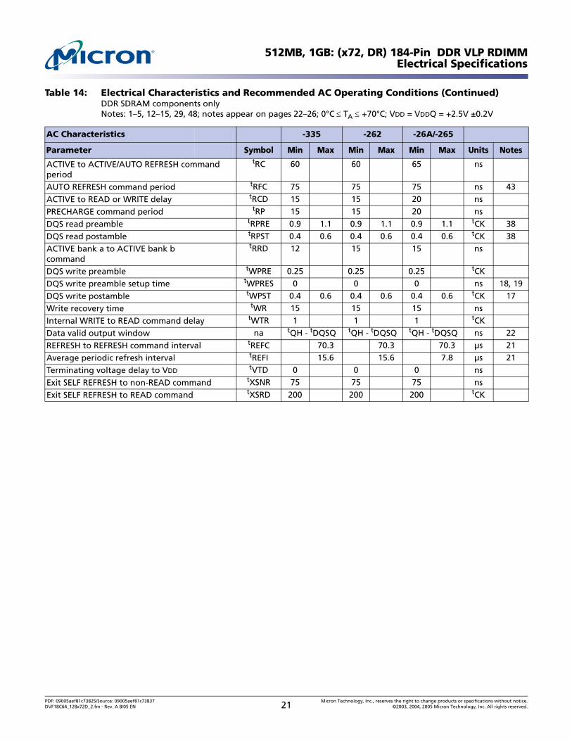
ACTIVE to ACTIVE/AUTO REFRESH command period
tRC 60 60 65 ns
AUTO REFRESH command period tRFC 75 75 75 ns 43
ACTIVE to READ or WRITE delay tRCD 15 15 20 ns
PRECHARGE command period tRP 15 15 20 ns
DQS read preamble tRPRE 0.9 1.1 0.9 1.1 0.9 1.1 tCK 38
DQS read postamble tRPST 0.4 0.6 0.4 0.6 0.4 0.6 tCK 38
ACTIVE bank a to ACTIVE bank b command
tRRD 12 15 15 ns
DQS write preamble tWPRE 0.25 0.25 0.25 tCK
DQS write preamble setup time tWPRES 0 0 0 ns 18, 19
DQS write postamble tWPST 0.4 0.6 0.4 0.6 0.4 0.6 tCK 17
Write recovery time tWR 15 15 15 ns
Internal WRITE to READ command delay tWTR 1 1 1 tCK
Data valid output window na tQH - tDQSQ tQH - tDQSQ tQH - tDQSQ ns 22
REFRESH to REFRESH command interval tREFC 70.3 70.3 70.3 µs 21
Average periodic refresh interval tREFI 15.6 15.6 7.8 µs 21
Terminating voltage delay to VDD tVTD 0 0 0 ns
Exit SELF REFRESH to non-READ command tXSNR 75 75 75 ns
Exit SELF REFRESH to READ command tXSRD 200 200 200 tCK
Table 14: Electrical Characteristics and Recommended AC Operating Conditions (Continued)DDR SDRAM components onlyNotes: 1–5, 12–15, 29, 48; notes appear on pages 22–26; 0°C ≤ TA ≤ +70°C; VDD = VDDQ = +2.5V ±0.2V
AC Characteristics -335 -262 -26A/-265
Parameter Symbol Min Max Min Max Min Max Units Notes
PDF: 09005aef81c73825/Source: 09005aef81c73837 Micron Technology, Inc., reserves the right to change products or specifications without notice.DVF18C64_128x72D_2.fm - Rev. A 8/05 EN 21 ©2003, 2004, 2005 Micron Technology, Inc. All rights reserved.
512MB, 1GB: (x72, DR) 184-Pin DDR VLP RDIMMNotes
Notes1. All voltages referenced to VSS.2. Tests for AC timing, IDD, and electrical AC and DC characteristics may be conducted
at nominal reference/supply voltage levels, but the related specifications and deviceoperation are guaranteed for the full voltage range specified.
3. Outputs measured with equivalent load:
4. AC timing and IDD tests may use a VIL-to-VIH swing of up to 1.5V in the test environment,but input timing is still referenced to VREF (or to the crossing point for CK/CK#), andparameter specifications are guaranteed for the specified AC input levels under normaluse conditions. The minimum slew rate for the input signals used to test the device is1V/ns in the range between VIL(AC) and VIH(AC).
5. The AC and DC input level specifications are as defined in the SSTL_2 Standard (i.e.,the receiver will effectively switch as a result of the signal crossing the AC input level,and will remain in that state as long as the signal does not ring back above [below] theDC input LOW [HIGH] level).
6. VREF is expected to equal VDDQ/2 of the transmitting device and to track variations inthe DC level of the same. Peak-to-peak noise (non-common mode) on VREF may notexceed ±2 percent of the DC value. Thus, from VDDQ/2, VREF is allowed ±25mV for DCerror and an additional ±25mV for AC noise. This measurement is to be taken at thenearest VREF by-pass capacitor.
7. VTT is not applied directly to the device. VTT is a system supply for signal terminationresistors, is expected to be set equal to VREF and must track variations in the DC levelof VREF.
8. IDD is dependent on output loading and cycle rates. Specified values are obtainedwith minimum cycle time at CL = 2 for -262, and -26A, CL = 2.5 for-335 and -265 withthe outputs open.
9. Enables on-chip refresh and address counters. 10. IDD specifications are tested after the device is properly initialized, and is averaged at
the defined cycle rate.11. This parameter is sampled. VDD = +2.5V ±0.2V, VDDQ = +2.5V ±0.2V, VREF = VSS, f = 100
MHz, TA = 25°C, VOUT(DC) = VDDQ/2, VOUT (peak to peak) = 0.2V. DM input is groupedwith I/O pins, reflecting the fact that they are matched in loading.
12. For slew rates less than 1 V/ns and greater than or equal to 0.5 V/ns. If slew rate is lessthan 0.5 V/ns, timing must be derated: tIS has an additional 50ps per each 100 mV/nsreduction in slew rate from 500 mV/ns, while tIH is unaffected. If slew rate exceeds 4.5V/ns, functionality is uncertain. For -335, slew rates must be ≥ 0.5 V/ns.
13. The CK/CK# input reference level (for timing referenced to CK/CK#) is the point atwhich CK and CK# cross; the input reference level for signals other than CK/CK# isVREF.
14. Inputs are not recognized as valid until VREF stabilizes. Exception: during the periodbefore VREF stabilizes, CKE ≤ 0.3 x VDDQ is recognized as LOW.
15. The output timing reference level, measured at the timing reference point indicated inNote 3, is VTT.
Output(VOUT)
Reference Point
50Ω
VTT
30pF
PDF: 09005aef81c73825/Source: 09005aef81c73837 Micron Technology, Inc., reserves the right to change products or specifications without notice.DVF18C64_128x72D_2.fm - Rev. A 8/05 EN 22 ©2003, 2004, 2005 Micron Technology, Inc. All rights reserved.
512MB, 1GB: (x72, DR) 184-Pin DDR VLP RDIMMNotes
16. tHZ and tLZ transitions occur in the same access time windows as valid data transi-tions. These parameters are not referenced to a specific voltage level, but specifywhen the device output is no longer driving (HZ) or begins driving (LZ).
17. The intent of the Don’t Care state after completion of the postamble is that the DQS-driven signal should either be high, low, or high-Z and that any signal transitionwithin the input switching region must follow valid input requirements. If DQS transi-tions to HIGH above VIH (DC) MIN, then it must not transition to LOW below VIH (DC)MIN prior to tDQSH (MIN).
18. This is not a device limit. The device will operate with a negative value, but systemperformance could be degraded due to bus turnaround.
19. It is recommended that DQS be valid (HIGH or LOW) on or before the WRITE com-mand. The case shown (DQS going from High-Z to logic LOW) applies when noWRITEs were previously in progress on the bus. If a previous WRITE was in progress,DQS could be HIGH during this time, depending on tDQSS.
20. MIN (tRC or tRFC) for IDD measurements is the smallest multiple of tCK that meets theminimum absolute value for the respective parameter. tRAS (MAX) for IDD measure-ments is the largest multiple of tCK that meets the maximum absolute value for tRAS.
21. The refresh period is 64ms. This equates to an average refresh rate of 7.8125µs. How-ever, an AUTO REFRESH command must be asserted at least once every 70.3µs; burstrefreshing or posting by the DRAM controller greater than eight refresh cycles is notallowed.
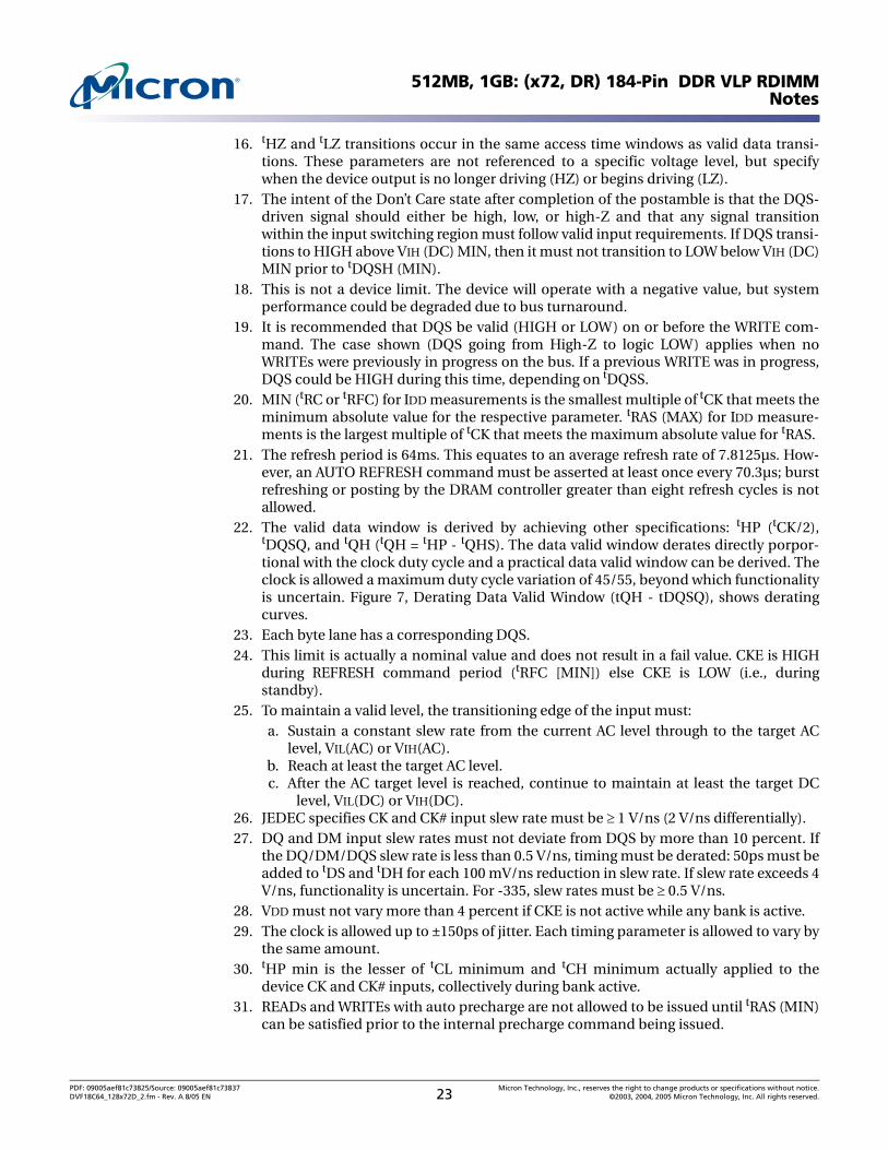
22. The valid data window is derived by achieving other specifications: tHP (tCK/2),tDQSQ, and tQH (tQH = tHP - tQHS). The data valid window derates directly porpor-tional with the clock duty cycle and a practical data valid window can be derived. Theclock is allowed a maximum duty cycle variation of 45/55, beyond which functionalityis uncertain. Figure 7, Derating Data Valid Window (tQH - tDQSQ), shows deratingcurves.
23. Each byte lane has a corresponding DQS.24. This limit is actually a nominal value and does not result in a fail value. CKE is HIGH
during REFRESH command period (tRFC [MIN]) else CKE is LOW (i.e., duringstandby).
25. To maintain a valid level, the transitioning edge of the input must:a. Sustain a constant slew rate from the current AC level through to the target AC
level, VIL(AC) or VIH(AC). b. Reach at least the target AC level. c. After the AC target level is reached, continue to maintain at least the target DC
level, VIL(DC) or VIH(DC).26. JEDEC specifies CK and CK# input slew rate must be ≥ 1 V/ns (2 V/ns differentially).27. DQ and DM input slew rates must not deviate from DQS by more than 10 percent. If
the DQ/DM/DQS slew rate is less than 0.5 V/ns, timing must be derated: 50ps must beadded to tDS and tDH for each 100 mV/ns reduction in slew rate. If slew rate exceeds 4V/ns, functionality is uncertain. For -335, slew rates must be ≥ 0.5 V/ns.
28. VDD must not vary more than 4 percent if CKE is not active while any bank is active.29. The clock is allowed up to ±150ps of jitter. Each timing parameter is allowed to vary by
the same amount. 30. tHP min is the lesser of tCL minimum and tCH minimum actually applied to the
device CK and CK# inputs, collectively during bank active. 31. READs and WRITEs with auto precharge are not allowed to be issued until tRAS (MIN)
can be satisfied prior to the internal precharge command being issued.
PDF: 09005aef81c73825/Source: 09005aef81c73837 Micron Technology, Inc., reserves the right to change products or specifications without notice.DVF18C64_128x72D_2.fm - Rev. A 8/05 EN 23 ©2003, 2004, 2005 Micron Technology, Inc. All rights reserved.
512MB, 1GB: (x72, DR) 184-Pin DDR VLP RDIMMNotes
Figure 7: Derating Data Valid Window (tQH - tDQSQ)
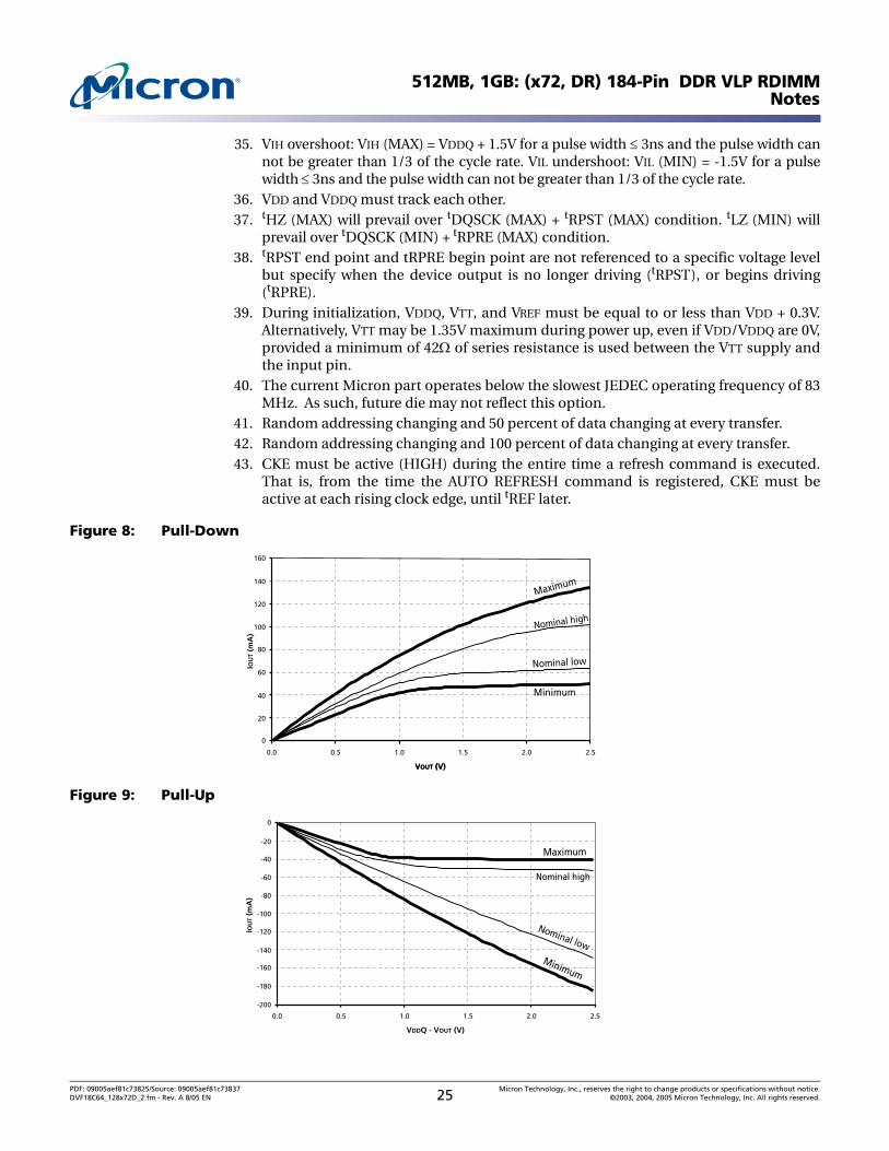
32. Any positive glitch in the nominal voltage must be less than 1/3 of the clock and notmore than +400mV or 2.9V max, whichever is less. Any negative glitch must be lessthan 1/3 of the clock cycle and not exceed either -300mV or 2.2V min, whichever ismore positive. However, the DC average cannot be below 2.3V minimum.
33. Normal Output Drive Curves: a. The full variation in driver pull-down current from minimum to maximum pro-
cess, temperature and voltage will lie within the outer bounding lines of the V-Icurve of Figure 8, "Pull-Down," on page 25.
b. The variation in driver pull-down current within nominal limits of voltage andtemperature is expected, but not guaranteed, to lie within the inner boundinglines of the V-I curve of Figure 8, "Pull-Down," on page 25.
c. The full variation in driver pull-up current from minimum to maximum process,temperature and voltage will lie within the outer bounding lines of the V-I curveof Figure 9, "Pull-Up," on page 25.
d. The variation in driver pull-up current within nominal limits of voltage and tem-perature is expected, but not guaranteed, to lie within the inner bounding linesof the V-I curve of Figure 9, "Pull-Up," on page 25.
e. The full variation in the ratio of the maximum to minimum pull-up and pull-down current should be between 0.71 and 1.4, for device drain-to-source volt-ages from 0.1V to 1.0V, and at the same voltage and temperature.
f. The full variation in the ratio of the nominal pull-up to pull-down current shouldbe unity ±10 percent, for device drain-to-source voltages from 0.1V to 1.0V.
34. The voltage levels used are derived from a minimum VDD level and the referenced testload. In practice, the voltage levels obtained from a properly terminated bus will pro-vide significantly different voltage values.
3.7503.700
3.6503.600
3.5503.500
3.4503.400
3.3503.300
3.250
2.500 2.4632.425
2.388 2.3502.313 2.275
2.2382.200 2.163
2.125
1.8
2.0
2.2
2.4
2.6
2.8
3.0
3.2
3.4
3.6
3.8
50/50 49.5/50.5 49/51 48.5/52.5 48/52 47.5/53.5 47/53 46.5/54.5 46/54 45.5/55.5 45/55
Clock Duty Cycle
ns
-335-262/-26A/-265 @ tCK = 10ns-262/-26A/-265 @ tCK = 7.5ns
NA
PDF: 09005aef81c73825/Source: 09005aef81c73837 Micron Technology, Inc., reserves the right to change products or specifications without notice.DVF18C64_128x72D_2.fm - Rev. A 8/05 EN 24 ©2003, 2004, 2005 Micron Technology, Inc. All rights reserved.
512MB, 1GB: (x72, DR) 184-Pin DDR VLP RDIMMNotes
35. VIH overshoot: VIH (MAX) = VDDQ + 1.5V for a pulse width ≤ 3ns and the pulse width cannot be greater than 1/3 of the cycle rate. VIL undershoot: VIL (MIN) = -1.5V for a pulsewidth ≤ 3ns and the pulse width can not be greater than 1/3 of the cycle rate.
36. VDD and VDDQ must track each other.37. tHZ (MAX) will prevail over tDQSCK (MAX) + tRPST (MAX) condition. tLZ (MIN) will
prevail over tDQSCK (MIN) + tRPRE (MAX) condition.38. tRPST end point and tRPRE begin point are not referenced to a specific voltage level
but specify when the device output is no longer driving (tRPST), or begins driving(tRPRE).
39. During initialization, VDDQ, VTT, and VREF must be equal to or less than VDD + 0.3V.Alternatively, VTT may be 1.35V maximum during power up, even if VDD/VDDQ are 0V,provided a minimum of 42Ω of series resistance is used between the VTT supply andthe input pin.
40. The current Micron part operates below the slowest JEDEC operating frequency of 83MHz. As such, future die may not reflect this option.
41. Random addressing changing and 50 percent of data changing at every transfer.42. Random addressing changing and 100 percent of data changing at every transfer.43. CKE must be active (HIGH) during the entire time a refresh command is executed.
That is, from the time the AUTO REFRESH command is registered, CKE must beactive at each rising clock edge, until tREF later.
Figure 8: Pull-Down
Figure 9: Pull-Up
160
140
IOU
T (m
A)
VOUT (V)
Nominal low
Minimum
Nominal high
Maximum
120
100
80
60
40
20
0
0.0 0.5 1.0 1.5 2.0 2.5
VOUT (V)
0
-20
IOU
T (m
A)
Nominal low
Minimum
Nominal high
Maximum-40
-60
-80
-100
-120
-140
-160
-180
-200
0.0 0.5 1.0 1.5 2.0 2.5
VDDQ - VOUT (V)
PDF: 09005aef81c73825/Source: 09005aef81c73837 Micron Technology, Inc., reserves the right to change products or specifications without notice.DVF18C64_128x72D_2.fm - Rev. A 8/05 EN 25 ©2003, 2004, 2005 Micron Technology, Inc. All rights reserved.
512MB, 1GB: (x72, DR) 184-Pin DDR VLP RDIMMNotes
44. IDD2N specifies the DQ, DQS, and DM to be driven to a valid high or low logic level.IDD2Q is similar to IDD2F except IDD2Q specifies the address and control inputs toremain stable. Although IDD2F, IDD2N, and IDD2Q are similar, IDD2F is “worst case.”
45. Whenever the operating frequency is altered, not including jitter, the DLL is requiredto be reset. This is followed by 200 clock cycles (before READ commands).
46. Leakage number reflects the worst case leakage possible through the module pin, notwhat each memory device contributes.
47. When an input signal is HIGH or LOW, it is defined as a steady state logic HIGH orLOW.
48. The -335 speed grade will operate with tRAS (MIN) = 40ns and tRAS (MAX) = 120,000nsat any slower frequency.
PDF: 09005aef81c73825/Source: 09005aef81c73837 Micron Technology, Inc., reserves the right to change products or specifications without notice.DVF18C64_128x72D_2.fm - Rev. A 8/05 EN 26 ©2003, 2004, 2005 Micron Technology, Inc. All rights reserved.
512MB, 1GB: (x72, DR) 184-Pin DDR VLP RDIMMInitialization
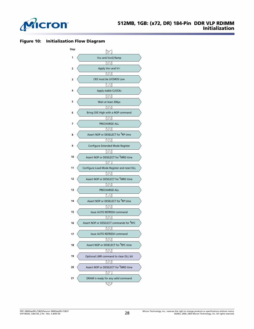
Initialization To ensure device operation the DRAM must be initialized as described below:
1. Simultaneously apply power to VDD and VDDQ.2. Apply VREF and then VTT power.3. Assert and hold CKE at a LVCMOS logic LOW.4. Provide stable clock signals.5. Wait at least 200µs.6. Bring CKE high and provide at least one NOP or DESELECT command. At this point
the CKE input changes from a LVCMOS input to a SSTL2 input only, and will remain a SSTL_2 input unless a power cycle occurs.
7. Perform a PRECHARGE ALL command.8. Wait at least tRP time, during which NOP or DESELECT commands must be given.9. Using the LMR command program the extended mode register (E0 = 0 to enable the
DLL and E1 = 0 for normal drive or E1 = 1 for reduced drive, E2 through En must be set to 0; where n = most significant bit).
10. Wait at least tMRD time; only NOP or DESELECT commands are allowed.11. Using the LMR command, program the mode register to set operating parameters
and to reset the DLL. At least 200 clock cycles are required between a DLL reset and any READ command.
12. Wait at least tMRD time; only NOP or DESELECT commands are allowed.13. Issue a PRECHARGE ALL command.14. Wait at least tRP time; only NOP or DESELECT commands are allowed.15. Issue an AUTO REFRESH command (this may be moved prior to step 13).16. Wait at least tRFC time; only NOP or DESELECT commands are allowed.17. Issue an AUTO REFRESH command (this may be moved prior to step 13).18. Wait at least tRFC time: only NOP or DESELECT commands are allowed.19. Although not required by the Micron device, JEDEC requires a LMR command to clear
the DLL bit (set M8 = 0). If a LMR command is issued the same operating parameters should be utilized as in step 11.
20. Wait at least tMRD time; only NOP or DESELECT commands are allowed.
At this point the module is ready for any valid command. Please note that 200 clock cycles must pass between step 11 (DLL Reset) and any READ command.
PDF: 09005aef81c73825/Source: 09005aef81c73837 Micron Technology, Inc., reserves the right to change products or specifications without notice.DVF18C64_128x72D_2.fm - Rev. A 8/05 EN 27 ©2003, 2004, 2005 Micron Technology, Inc. All rights reserved.
512MB, 1GB: (x72, DR) 184-Pin DDR VLP RDIMMInitialization
Figure 10: Initialization Flow Diagram
VDD and VDDQ Ramp
Apply VREF and VTT
CKE must be LVCMOS Low
Apply stable CLOCKs
Bring CKE High with a NOP command
Wait at least 200µs
PRECHARGE ALL
Assert NOP or DESELECT for tRP time
Configure Extended Mode Register
Configure Load Mode Register and reset DLL
Assert NOP or DESELECT for tMRD time
Assert NOP or DESELECT for tMRD time
PRECHARGE ALL
Issue AUTO REFRESH command
Assert NOP or DESELECT for tRFC time
Optional LMR command to clear DLL bit
Assert NOP or DESELECT for tMRD time
DRAM is ready for any valid command
Step
1
2
3
4
5
6
7
8
9
10
11
12
13
14
15
16
17
18
19
20
21
Assert NOP or DESELECT commands for tRFC
Issue AUTO REFRESH command
Assert NOP or DESELECT for tRP time
PDF: 09005aef81c73825/Source: 09005aef81c73837 Micron Technology, Inc., reserves the right to change products or specifications without notice.DVF18C64_128x72D_2.fm - Rev. A 8/05 EN 28 ©2003, 2004, 2005 Micron Technology, Inc. All rights reserved.
512MB, 1GB: (x72, DR) 184-Pin DDR VLP RDIMMRegister and PLL Specifications
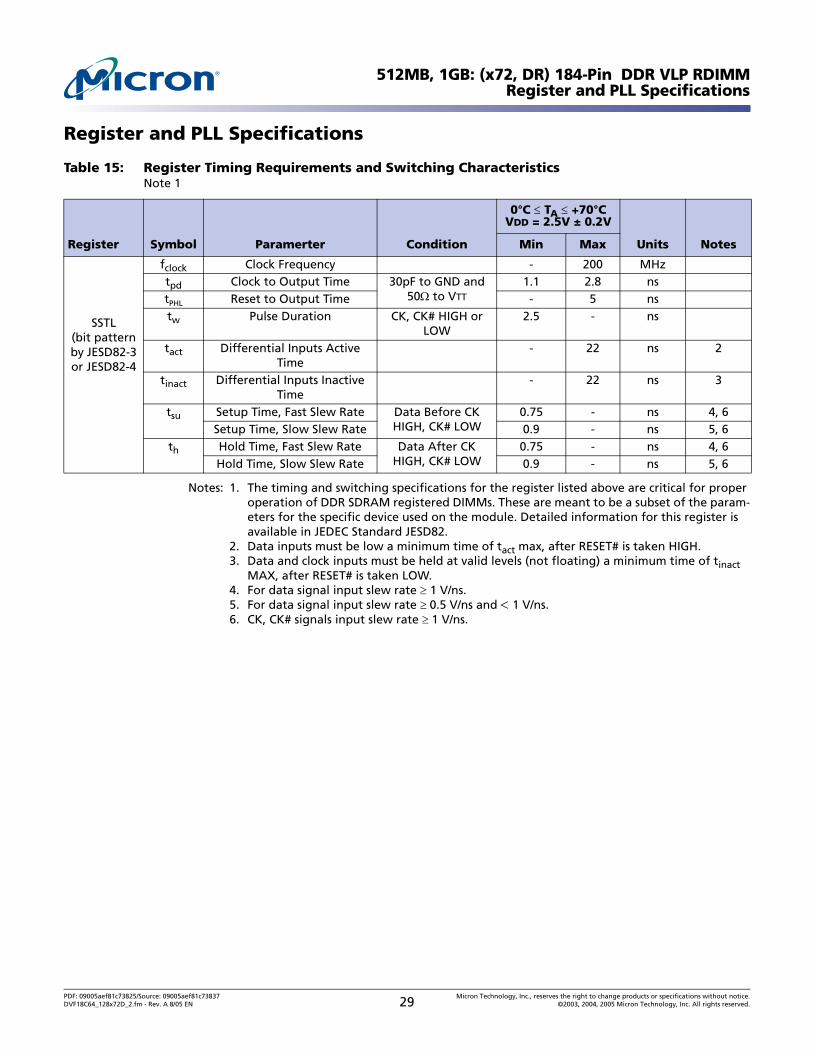
Register and PLL Specifications
Notes: 1. The timing and switching specifications for the register listed above are critical for proper operation of DDR SDRAM registered DIMMs. These are meant to be a subset of the param-eters for the specific device used on the module. Detailed information for this register is available in JEDEC Standard JESD82.
2. Data inputs must be low a minimum time of tact max, after RESET# is taken HIGH.3. Data and clock inputs must be held at valid levels (not floating) a minimum time of tinact
MAX, after RESET# is taken LOW.4. For data signal input slew rate ≥ 1 V/ns.5. For data signal input slew rate ≥ 0.5 V/ns and < 1 V/ns.6. CK, CK# signals input slew rate ≥ 1 V/ns.
Table 15: Register Timing Requirements and Switching CharacteristicsNote 1
Register Symbol Paramerter Condition
0°C ≤ TA ≤ +70°CVDD = 2.5V ± 0.2V
Units NotesMin Max
SSTL(bit pattern by JESD82-3 or JESD82-4
fclock Clock Frequency - 200 MHztpd Clock to Output Time 30pF to GND and
50Ω to VTT
1.1 2.8 nstPHL Reset to Output Time - 5 nstw Pulse Duration CK, CK# HIGH or
LOW2.5 - ns
tact Differential Inputs Active Time
- 22 ns 2
tinact Differential Inputs Inactive Time
- 22 ns 3
tsu Setup Time, Fast Slew Rate Data Before CK HIGH, CK# LOW
0.75 - ns 4, 6Setup Time, Slow Slew Rate 0.9 - ns 5, 6
th Hold Time, Fast Slew Rate Data After CK HIGH, CK# LOW
0.75 - ns 4, 6Hold Time, Slow Slew Rate 0.9 - ns 5, 6
PDF: 09005aef81c73825/Source: 09005aef81c73837 Micron Technology, Inc., reserves the right to change products or specifications without notice.DVF18C64_128x72D_2.fm - Rev. A 8/05 EN 29 ©2003, 2004, 2005 Micron Technology, Inc. All rights reserved.
512MB, 1GB: (x72, DR) 184-Pin DDR VLP RDIMMRegister and PLL Specifications
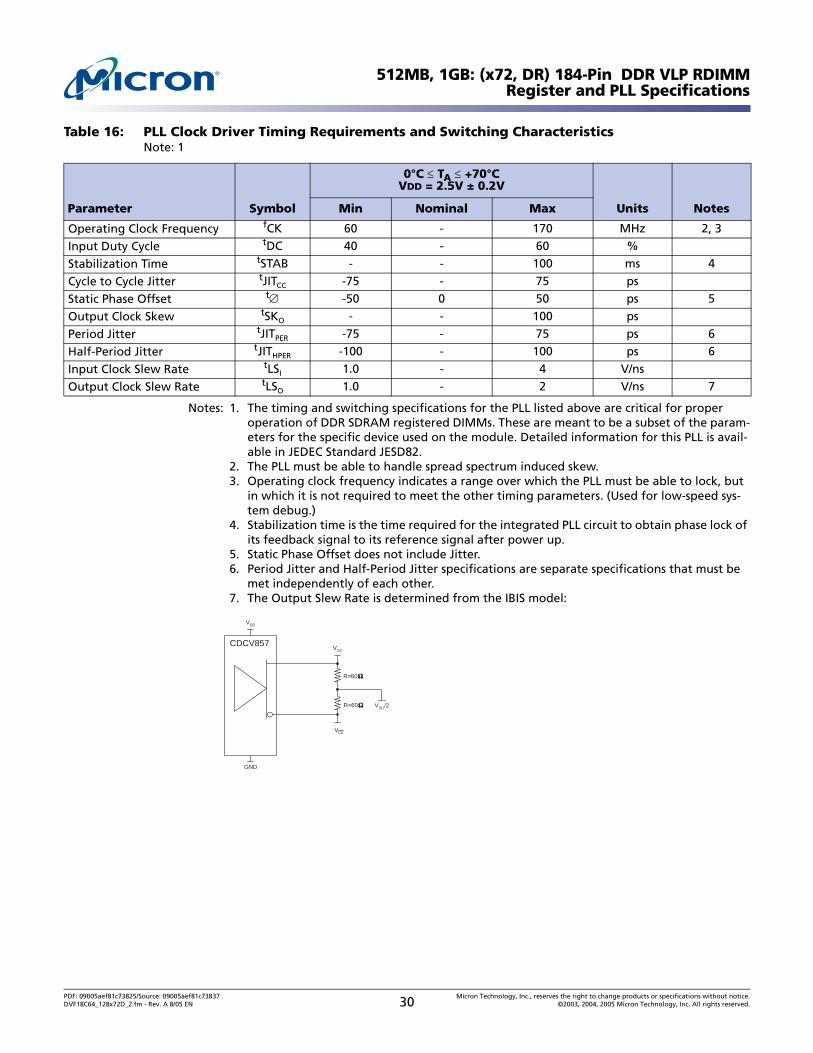
Notes: 1. The timing and switching specifications for the PLL listed above are critical for proper operation of DDR SDRAM registered DIMMs. These are meant to be a subset of the param-eters for the specific device used on the module. Detailed information for this PLL is avail-able in JEDEC Standard JESD82.
2. The PLL must be able to handle spread spectrum induced skew.3. Operating clock frequency indicates a range over which the PLL must be able to lock, but
in which it is not required to meet the other timing parameters. (Used for low-speed sys-tem debug.)
4. Stabilization time is the time required for the integrated PLL circuit to obtain phase lock of its feedback signal to its reference signal after power up.
5. Static Phase Offset does not include Jitter.6. Period Jitter and Half-Period Jitter specifications are separate specifications that must be
met independently of each other.7. The Output Slew Rate is determined from the IBIS model:
Table 16: PLL Clock Driver Timing Requirements and Switching CharacteristicsNote: 1
Parameter Symbol
0°C ≤ TA ≤ +70°CVDD = 2.5V ± 0.2V
Units NotesMin Nominal Max
Operating Clock Frequency fCK 60 - 170 MHz 2, 3
Input Duty Cycle tDC 40 - 60 %
Stabilization Time tSTAB - - 100 ms 4
Cycle to Cycle Jitter tJITCC -75 - 75 ps
Static Phase Offset t∅ -50 0 50 ps 5
Output Clock Skew tSKO - - 100 ps
Period Jitter tJITPER -75 - 75 ps 6
Half-Period Jitter tJITHPER -100 - 100 ps 6
Input Clock Slew Rate tLSI 1.0 - 4 V/ns
Output Clock Slew Rate tLSO 1.0 - 2 V/ns 7
VDD/2
GND
VDD
CDCV857
R=60ΩΩΩΩ
R=60ΩΩΩΩ
VCK
VCK
PDF: 09005aef81c73825/Source: 09005aef81c73837 Micron Technology, Inc., reserves the right to change products or specifications without notice.DVF18C64_128x72D_2.fm - Rev. A 8/05 EN 30 ©2003, 2004, 2005 Micron Technology, Inc. All rights reserved.
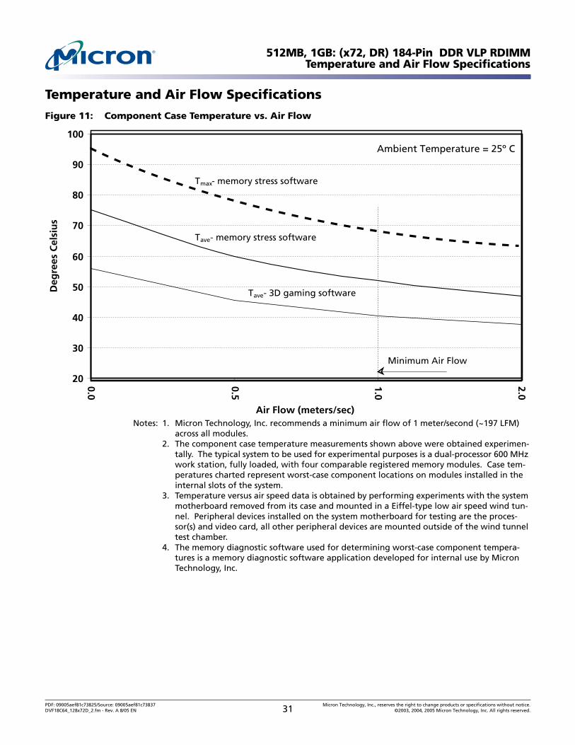
512MB, 1GB: (x72, DR) 184-Pin DDR VLP RDIMMTemperature and Air Flow Specifications
Temperature and Air Flow Specifications
Figure 11: Component Case Temperature vs. Air Flow
Notes: 1. Micron Technology, Inc. recommends a minimum air flow of 1 meter/second (~197 LFM) across all modules.
2. The component case temperature measurements shown above were obtained experimen-tally. The typical system to be used for experimental purposes is a dual-processor 600 MHz work station, fully loaded, with four comparable registered memory modules. Case tem-peratures charted represent worst-case component locations on modules installed in the internal slots of the system.
3. Temperature versus air speed data is obtained by performing experiments with the system motherboard removed from its case and mounted in a Eiffel-type low air speed wind tun-nel. Peripheral devices installed on the system motherboard for testing are the proces-sor(s) and video card, all other peripheral devices are mounted outside of the wind tunnel test chamber.
4. The memory diagnostic software used for determining worst-case component tempera-tures is a memory diagnostic software application developed for internal use by Micron Technology, Inc.
20
30
40
50
60
70
80
90
100
0.0
0.5
1.0
2.0
Air Flow (meters/sec)
Deg
rees
Cel
siu
s
Ambient Temperature = 25º C
Tmax - memory stress software
Tave - 3D gaming software
Tave - memory stress software
Minimum Air Flow
PDF: 09005aef81c73825/Source: 09005aef81c73837 Micron Technology, Inc., reserves the right to change products or specifications without notice.DVF18C64_128x72D_2.fm - Rev. A 8/05 EN 31 ©2003, 2004, 2005 Micron Technology, Inc. All rights reserved.
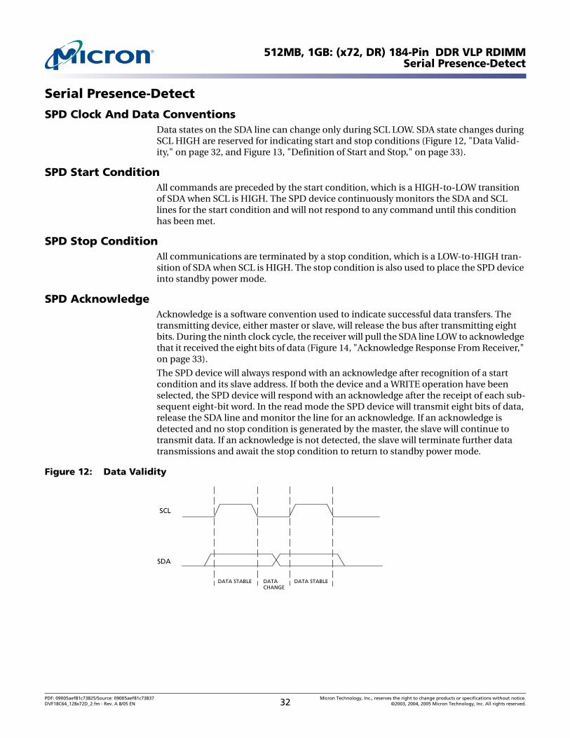
512MB, 1GB: (x72, DR) 184-Pin DDR VLP RDIMMSerial Presence-Detect
Serial Presence-Detect
SPD Clock And Data ConventionsData states on the SDA line can change only during SCL LOW. SDA state changes during SCL HIGH are reserved for indicating start and stop conditions (Figure 12, "Data Valid-ity," on page 32, and Figure 13, "Definition of Start and Stop," on page 33).
SPD Start ConditionAll commands are preceded by the start condition, which is a HIGH-to-LOW transition of SDA when SCL is HIGH. The SPD device continuously monitors the SDA and SCL lines for the start condition and will not respond to any command until this condition has been met.
SPD Stop ConditionAll communications are terminated by a stop condition, which is a LOW-to-HIGH tran-sition of SDA when SCL is HIGH. The stop condition is also used to place the SPD device into standby power mode.
SPD AcknowledgeAcknowledge is a software convention used to indicate successful data transfers. The transmitting device, either master or slave, will release the bus after transmitting eight bits. During the ninth clock cycle, the receiver will pull the SDA line LOW to acknowledge that it received the eight bits of data (Figure 14, "Acknowledge Response From Receiver," on page 33).
The SPD device will always respond with an acknowledge after recognition of a start condition and its slave address. If both the device and a WRITE operation have been selected, the SPD device will respond with an acknowledge after the receipt of each sub-sequent eight-bit word. In the read mode the SPD device will transmit eight bits of data, release the SDA line and monitor the line for an acknowledge. If an acknowledge is detected and no stop condition is generated by the master, the slave will continue to transmit data. If an acknowledge is not detected, the slave will terminate further data transmissions and await the stop condition to return to standby power mode.
Figure 12: Data Validity
SCL
SDA
DATA STABLE DATA STABLEDATACHANGE
PDF: 09005aef81c73825/Source: 09005aef81c73837 Micron Technology, Inc., reserves the right to change products or specifications without notice.DVF18C64_128x72D_2.fm - Rev. A 8/05 EN 32 ©2003, 2004, 2005 Micron Technology, Inc. All rights reserved.
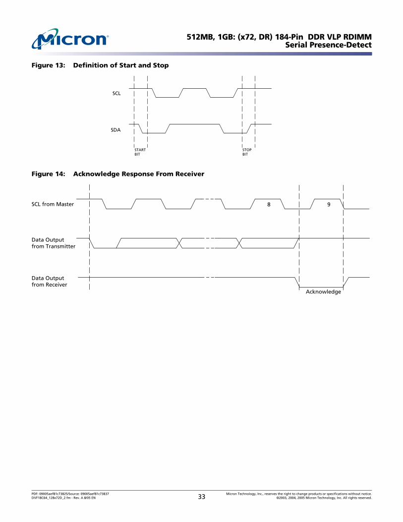
512MB, 1GB: (x72, DR) 184-Pin DDR VLP RDIMMSerial Presence-Detect
Figure 13: Definition of Start and Stop
Figure 14: Acknowledge Response From Receiver
SCL
SDA
STARTBIT
STOPBIT
SCL from Master
Data Outputfrom Transmitter
Data Outputfrom Receiver
98
Acknowledge
PDF: 09005aef81c73825/Source: 09005aef81c73837 Micron Technology, Inc., reserves the right to change products or specifications without notice.DVF18C64_128x72D_2.fm - Rev. A 8/05 EN 33 ©2003, 2004, 2005 Micron Technology, Inc. All rights reserved.
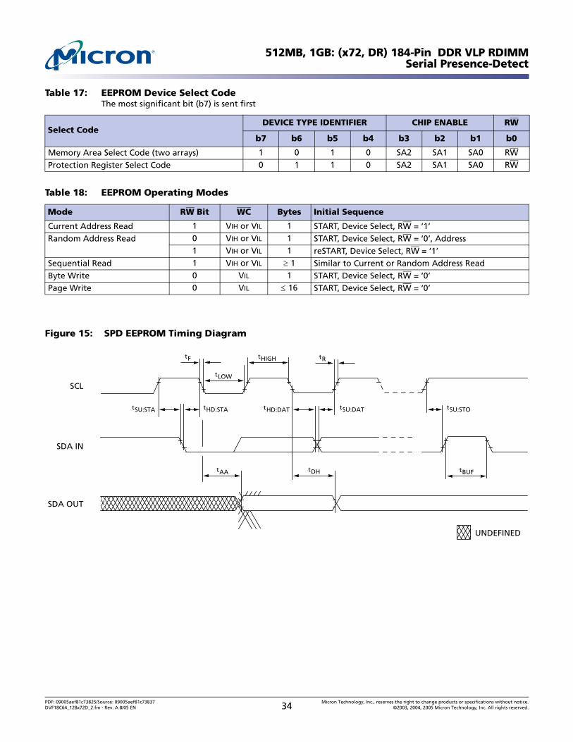
512MB, 1GB: (x72, DR) 184-Pin DDR VLP RDIMMSerial Presence-Detect
Figure 15: SPD EEPROM Timing Diagram
Table 17: EEPROM Device Select CodeThe most significant bit (b7) is sent first
Select CodeDEVICE TYPE IDENTIFIER CHIP ENABLE RW
b7 b6 b5 b4 b3 b2 b1 b0
Memory Area Select Code (two arrays) 1 0 1 0 SA2 SA1 SA0 RW
Protection Register Select Code 0 1 1 0 SA2 SA1 SA0 RW
Table 18: EEPROM Operating Modes
Mode RW Bit WC Bytes Initial Sequence
Current Address Read 1 VIH or VIL 1 START, Device Select, RW = ‘1’Random Address Read 0 VIH or VIL 1 START, Device Select, RW = ‘0’, Address
1 VIH or VIL 1 reSTART, Device Select, RW = ‘1’Sequential Read 1 VIH or VIL ≥ 1 Similar to Current or Random Address ReadByte Write 0 VIL 1 START, Device Select, RW = ‘0’Page Write 0 VIL ≤ 16 START, Device Select, RW = ‘0’
SCL
SDA IN
SDA OUT
tLOW
tSU:STA tHD:STA
tF tHIGH tR
tBUFtDHtAA
tSU:STOtSU:DATtHD:DAT
UNDEFINED
PDF: 09005aef81c73825/Source: 09005aef81c73837 Micron Technology, Inc., reserves the right to change products or specifications without notice.DVF18C64_128x72D_2.fm - Rev. A 8/05 EN 34 ©2003, 2004, 2005 Micron Technology, Inc. All rights reserved.
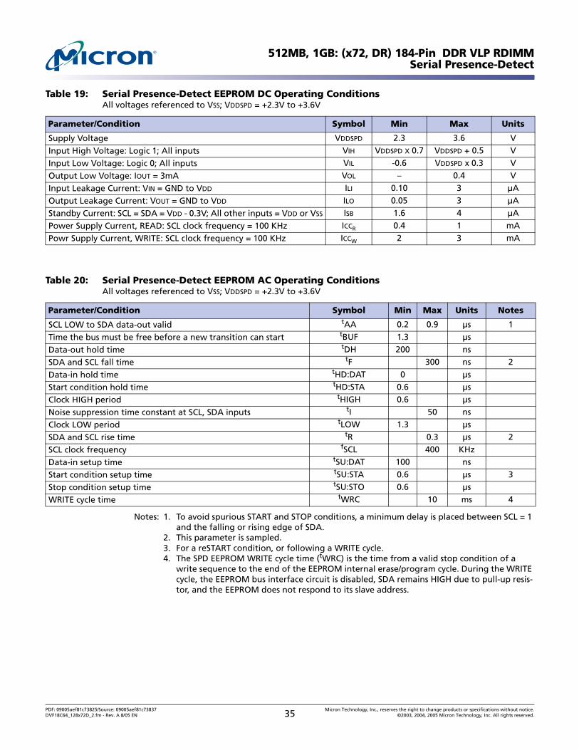
512MB, 1GB: (x72, DR) 184-Pin DDR VLP RDIMMSerial Presence-Detect
Notes: 1. To avoid spurious START and STOP conditions, a minimum delay is placed between SCL = 1 and the falling or rising edge of SDA.
2. This parameter is sampled.3. For a reSTART condition, or following a WRITE cycle.4. The SPD EEPROM WRITE cycle time (tWRC) is the time from a valid stop condition of a
write sequence to the end of the EEPROM internal erase/program cycle. During the WRITE cycle, the EEPROM bus interface circuit is disabled, SDA remains HIGH due to pull-up resis-tor, and the EEPROM does not respond to its slave address.
Table 19: Serial Presence-Detect EEPROM DC Operating ConditionsAll voltages referenced to VSS; VDDSPD = +2.3V to +3.6V
Parameter/Condition Symbol Min Max Units
Supply Voltage VDDSPD 2.3 3.6 V
Input High Voltage: Logic 1; All inputs VIH VDDSPD X 0.7 VDDSPD + 0.5 V
Input Low Voltage: Logic 0; All inputs VIL -0.6 VDDSPD x 0.3 V
Output Low Voltage: IOUT = 3mA VOL – 0.4 V
Input Leakage Current: VIN = GND to VDD ILI 0.10 3 µA
Output Leakage Current: VOUT = GND to VDD ILO 0.05 3 µA
Standby Current: SCL = SDA = VDD - 0.3V; All other inputs = VDD or VSS ISB 1.6 4 µA
Power Supply Current, READ: SCL clock frequency = 100 KHz ICCR 0.4 1 mA
Powr Supply Current, WRITE: SCL clock frequency = 100 KHz ICCW 2 3 mA
Table 20: Serial Presence-Detect EEPROM AC Operating ConditionsAll voltages referenced to VSS; VDDSPD = +2.3V to +3.6V
Parameter/Condition Symbol Min Max Units Notes
SCL LOW to SDA data-out valid tAA 0.2 0.9 µs 1
Time the bus must be free before a new transition can start tBUF 1.3 µs
Data-out hold time tDH 200 ns
SDA and SCL fall time tF 300 ns 2
Data-in hold time tHD:DAT 0 µs
Start condition hold time tHD:STA 0.6 µs
Clock HIGH period tHIGH 0.6 µs
Noise suppression time constant at SCL, SDA inputs tI 50 ns
Clock LOW period tLOW 1.3 µs
SDA and SCL rise time tR 0.3 µs 2
SCL clock frequency fSCL 400 KHz
Data-in setup time tSU:DAT 100 ns
Start condition setup time tSU:STA 0.6 µs 3
Stop condition setup time tSU:STO 0.6 µs
WRITE cycle time tWRC 10 ms 4
PDF: 09005aef81c73825/Source: 09005aef81c73837 Micron Technology, Inc., reserves the right to change products or specifications without notice.DVF18C64_128x72D_2.fm - Rev. A 8/05 EN 35 ©2003, 2004, 2005 Micron Technology, Inc. All rights reserved.
512MB, 1GB: (x72, DR) 184-Pin DDR VLP RDIMMSerial Presence-Detect
Table 21: Serial Presence-Detect Matrix“1”/“0”: Serial Data, “driven to HIGH”/“driven to LOW”; notes appear on page 37
Byte Description Entry (Version) MT18VDVF6472D MT18VDVF12872D
0 Number of SPD Bytes used by Micron 128 80 801 Total Number of Bytes in SPD Device 256 08 082 Fundamental Memory Type SDRAM DDR 07 073 Number of Row Addresses on Assembly 13 0D 0D4 Number of Column Addresses on Assembly 10 or 11 0A 0B5 Number of Physical Ranks on DIMM 2 02 026 Module Data Width 72 48 487 Module Data Width (Continued) 0 00 008 Module Voltage Interface Levels SSTL 2.5V 04 049 SDRAM Cycle Time, tCK (CAS Latency = 2.5) (See
note 1)6ns (-335)
7ns (-262/-26A)7.5ns (-265)
607075
607075
10 SDRAM Access from Clock,tAC(CAS Latency = 2.5)
0.7ns (-335)0.75ns (-262/-26A/-265)
7075
7075
11 Module Configuration Type ECC 02 0212 Refresh Rate/Type 7.81µs/SELF 82 8213 SDRAM Device Width (Primary SDRAM) 8 08 0814 Error-checking SDRAM Data Width 8 08 0815 Minimum Clock Delay, Back-to-Back Random
Column Access1 clock 01 01
16 Burst Lengths Supported 2, 4, 8 0E 0E17 Number of Banks on SDRAM Device 4 04 0418 CAS Latencies Supported 2, 2.5 0C 0C19 CS Latency 0 01 0120 WE Latency 1 02 0221 SDRAM Module Attributes Reg./Diff. Clk/PLL 26 2622 SDRAM Device Attributes: General Fast/Concurrent AP C0 C023 SDRAM Cycle Time, tCK (CAS Latency = 2) 7.5ns (-335/-262/-26A)
10ns (-265)75A0
75A0
24 SDRAM Access from CK, tAC (CAS Latency = 2)
0.70ns (-335)0.75ns (-262/-26A/-265)
7075
7075
25 SDRAM Cycle Time, tCK, (CAS Latency = 1.5) N/A 00 0026 SDRAM Access from CK, tAC, (CAS Latency = 1.5) N/A 00 0027 Minimum Row Precharge Time, tRP 18ns (-335)
15ns (-262)20ns (-26A/-265)
483C50
483C50
28 Minimum Row Active to Row Active, (RRD 12ns (-335)15ns (-262/-26A/-265)
303C
303C
29 Minimum RAS# to CAS# Delay, tRCD 18ns (-335)15ns (-262)
20ns (-26A/-265)
483C50
483C50
30 Minimum RAS# Pulse Width, tRAS (See note 2) 42ns (-335)45ns (-262/-26A/-265)
2A2D
2A2D
31 Module Rank Density 256MB, 512MB 40 8032 Address and Command Setup Time, tIS (See note
3)0.80ns (-335)
1ns (262/-26A/-265)80A0
80A0
PDF: 09005aef81c73825/Source: 09005aef81c73837 Micron Technology, Inc., reserves the right to change products or specifications without notice.DVF18C64_128x72D_2.fm - Rev. A 8/05 EN 36 ©2003, 2004, 2005 Micron Technology, Inc. All rights reserved.
512MB, 1GB: (x72, DR) 184-Pin DDR VLP RDIMMSerial Presence-Detect
Notes: 1. Value for -26A tCK set to 7ns (0x70) for optimum BIOS compatibility. Actual device specifi-cation vaule is 7.5ns.
2. The value of tRAS used for -26A/-265 modules is calculated from tRC - tRP. Actual device specification value is 40 ns.
3. The JEDEC SPD specification allows fast or slow slew rate values for these bytes. The worst-case (slow slew rate) value is repesented here. Systems requiring the fast slew rate setup and hold values are supported, provided the faster minimum slew rate is met.
33 Address and Command Hold Time, tIH (See note 3)
0.80ns (-335)1ns (-262/-26A/-265)
80A0
80A0
34 Data/Data Mask Input Setup Time, tDS 0.45ns (-335)0.50ns (-262/-26A/-265)
4550
4550
35 Data/Data Mask Input Hold Time, tDH 0.45ns (-335)0.50ns (-262/-26A/-265)
4550
4550
36-40 Reserved 00 0041 Minimum Active Auto Refresh Time tRC 60ns (-335/-262)
65ns (-26A/-265)3C41
3C41
42 Minimum Auto Refresh to Active/Auto Refresh Command Period, tRFC
72ns (-335)75ns (-262/-26A/-265)
484B
484B
43 SDRAM Device Max Cycle Time tCKMAX 12ns (-335)13ns (-262/-26A/-265)
3034
3034
44 SDRAM Device Max DQS-DQ Skew Time, tDQSQ 0.40ns (-335)0.5ns (-262/-26A/-265)
2832
2832
45 SDRAM Device Max Read Data Hold Skew Factor, tQHS
0.50ns (-335)0.75ns (-262/-26A/-265)
5075
5075
46 Reserved 00 0047 DIMM Height 11 11
48–61 Reserved 00 0062 SPD Revision Release 1.0 10 1063 Checksum for Bytes 0–62 -335
-262-26A-265
46E31040
87245181
64 Manufacturer’s JEDEC ID Code MICRON 2C 2C65-71 Manufacturer’s JEDEC ID Code (Continued) FF FF
72 Manufacturing Location 01–12 01–0C 01–0C73-90 Module Part Number (ASCII) Variable Data Variable Data
91 PCB Identification Code 1-9 01-09 01-0992 Identification Code (Continued) 0 00 0093 Year of Manufacture in BCD Variable Data Variable Data94 Week of Manufacture in BCD Variable Data Variable Data
95-98 Module Serial Number Variable Data Variable Data99-127 Manufacturer-specific Data (RSVD) – –
Table 21: Serial Presence-Detect Matrix (Continued)“1”/“0”: Serial Data, “driven to HIGH”/“driven to LOW”; notes appear on page 37
Byte Description Entry (Version) MT18VDVF6472D MT18VDVF12872D
PDF: 09005aef81c73825/Source: 09005aef81c73837 Micron Technology, Inc., reserves the right to change products or specifications without notice.DVF18C64_128x72D_2.fm - Rev. A 8/05 EN 37 ©2003, 2004, 2005 Micron Technology, Inc. All rights reserved.
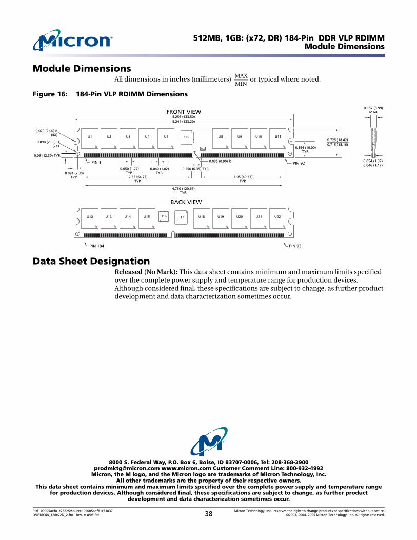
512MB, 1GB: (x72, DR) 184-Pin DDR VLP RDIMMModule Dimensions
Module DimensionsAll dimensions in inches (millimeters) or typical where noted.
Figure 16: 184-Pin VLP RDIMM Dimensions
Data Sheet DesignationReleased (No Mark): This data sheet contains minimum and maximum limits specified over the complete power supply and temperature range for production devices. Although considered final, these specifications are subject to change, as further product development and data characterization sometimes occur.
MAXMIN
0.725 (18.42)0.715 (18.16)
PIN 1
0.098 (2.50) D(2X)
0.091 (2.30) TYP.
0.250 (6.35) TYP.
4.750 (120.65)TYP.
0.050 (1.27)TYP.0.091 (2.30)
TYP.
0.040 (1.02)TYP.
0.079 (2.00) R(4X)
0.035 (0.90) R PIN 92
FRONT VIEW5.256 (133.50)5.244 (133.20)
2.55 (64.77)TYP.
1.95 (49.53)TYP.
0.394 (10.00)TYP.
BACK VIEW
PIN 184 PIN 93
0.054 (1.37)0.046 (1.17)
0.157 (3.99)MAX
U11U1 U2 U3 U4 U5 U6
U7
U8 U9 U10 U11
U16 U17U12 U13 U14 U15 U18 U19 U20 U21 U22
®
8000 S. Federal Way, P.O. Box 6, Boise, ID 83707-0006, Tel: [email protected] www.micron.com Customer Comment Line: 800-932-4992
Micron, the M logo, and the Micron logo are trademarks of Micron Technology, Inc. All other trademarks are the property of their respective owners.
This data sheet contains minimum and maximum limits specified over the complete power supply and temperature range for production devices. Although considered final, these specifications are subject to change, as further product
development and data characterization sometimes occur.
PDF: 09005aef81c73825/Source: 09005aef81c73837 Micron Technology, Inc., reserves the right to change products or specifications without notice.DVF18C64_128x72D_2.fm - Rev. A 8/05 EN 38 ©2003, 2004, 2005 Micron Technology, Inc. All rights reserved.