Embed Size (px)
Citation preview

DDR PHY Interface (DFI) Specification
Version 2.1 (Preliminary)30 January 2009
DENALI SOFTWARE, INC.1000 Hamlin Court
Sunnyvale, CA 94089Tel: (408) 743-4200Fax: (408) 743-4209
Copyright 1995-2008, Denali Software, Inc.
[email protected]@denali.com
www.denali.com/supportwww.ememory.com
All Rights Reserved
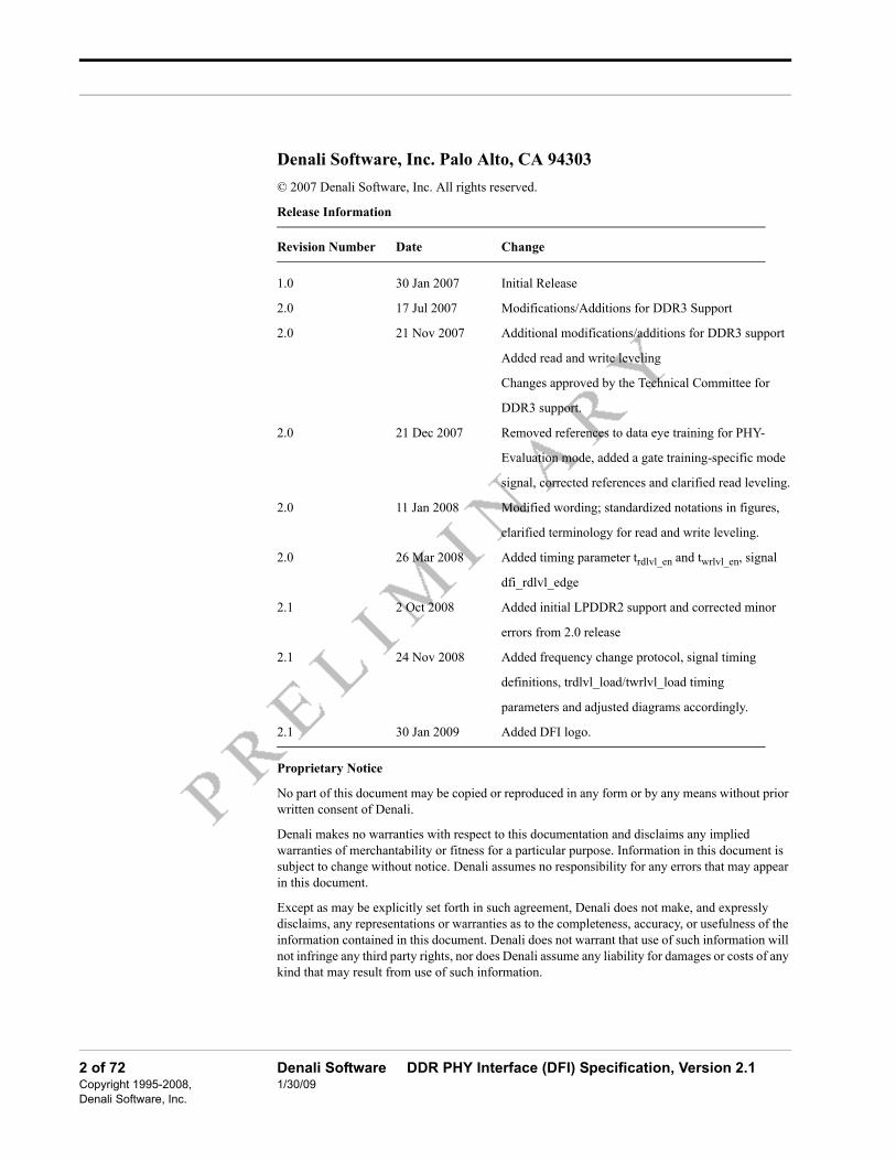
Denali Software, Inc. Palo Alto, CA 94303
© 2007 Denali Software, Inc. All rights reserved.
Release Information
Revision Number Date Change
1.0 30 Jan 2007 Initial Release
2.0 17 Jul 2007 Modifications/Additions for DDR3 Support
2.0 21 Nov 2007 Additional modifications/additions for DDR3 support
Added read and write leveling
Changes approved by the Technical Committee for
DDR3 support.
2.0 21 Dec 2007 Removed references to data eye training for PHY-
Evaluation mode, added a gate training-specific mode
signal, corrected references and clarified read leveling.
2.0 11 Jan 2008 Modified wording; standardized notations in figures,
clarified terminology for read and write leveling.
2.0 26 Mar 2008 Added timing parameter trdlvl_en and twrlvl_en, signal
dfi_rdlvl_edge
2.1 2 Oct 2008 Added initial LPDDR2 support and corrected minor
errors from 2.0 release
2.1 24 Nov 2008 Added frequency change protocol, signal timing
definitions, trdlvl_load/twrlvl_load timing
parameters and adjusted diagrams accordingly.
2.1 30 Jan 2009 Added DFI logo.
Proprietary Notice
No part of this document may be copied or reproduced in any form or by any means without prior written consent of Denali.
Denali makes no warranties with respect to this documentation and disclaims any implied warranties of merchantability or fitness for a particular purpose. Information in this document is subject to change without notice. Denali assumes no responsibility for any errors that may appear in this document.
Except as may be explicitly set forth in such agreement, Denali does not make, and expressly disclaims, any representations or warranties as to the completeness, accuracy, or usefulness of the information contained in this document. Denali does not warrant that use of such information will not infringe any third party rights, nor does Denali assume any liability for damages or costs of any kind that may result from use of such information.
2 of 72 Denali Software DDR PHY Interface (DFI) Specification, Version 2.1Copyright 1995-2008, 1/30/09Denali Software, Inc.

RESTRICTED RIGHTS LEGEND
Use, duplication, or disclosure by the Government is subject to restrictions as set forth in subparagraphs (c)(1)(ii) of the Rights in Technical Data and Computer Software clause at DFARS 252.227-7013.
Destination Control Statement
All technical data contained in this product is subject to the export control laws of the United States of America. Disclosure to nationals of other countries contrary to United States law is prohibited. It is the reader’s responsibility to determine the applicable regulations and to comply with them.
Trademarks
Denali and the Denali logo are registered trademarks of Denali Software, Inc.
All other products or brand names mentioned are trademarks or registered trademarks of their respective holders.
End User License Agreement
1. Subject to the provisions of Clauses 2, 3, 4, 5 and 6, Denali hereby grants to licensee (“Licensee”) a perpetual, non-exclusive, nontransferable, royalty free, worldwide copyright license to use and copy the DFI (DDR PHY Interface) specification (the “DFI Specification”) for the purpose of developing, having developed, manufacturing, having manufactured, offering to sell, selling, supplying or otherwise distributing products which comply with the DFI Specification.
2. THE DFI SPECIFICATION IS PROVIDED “AS IS” WITH NO WARRANTIES EXPRESS, IMPLIED OR STATUTORY, INCLUDING BUT NOT LIMITED TO ANY WARRANTY OF SATISFACTORY QUALITY, MERCHANTABILITY, NONINFRINGEMENT OR FITNESS FOR A PARTICULAR PURPOSE.
3. No license, express, implied or otherwise, is granted to Licensee, under the provisions of Clause 1, to use Denali's or any other person or entity participating in the development of the DFI Specification listed herein (individually “Participant,” collectively “Participants”) trade name, or trademarks in connection with the DFI Specification or any products based thereon. Nothing in Clause 1 shall be construed as authority for Licensee to make any representations on behalf of Denali or the other Participants in respect of the DFI Specification.
4. NOTWITHSTANDING ANYTHING ELSE WILL DENALI'S TOTAL AGGREGATE LIABILITY FOR ANY CLAIM, SUIT, PROCEEDING OR OTHERWISE, RELATING IN ANYWAY TO THE DFI SPECIFICATION EXCEED $1.00USD.
5. NOTWITHSTANDING ANYTHING ELSE WILL ANY PARTICIPANT'S TOTAL AGGREGATE LIABILITY FOR ANY CLAIM, SUIT, PROCEEDING OR OTHERWISE, RELATING IN ANYWAY TO THE DFI SPECIFICATION EXCEED $1.00USD.
6. Licensee agrees that Denali and the Participants may use, copy, modify, reproduce and distribute any written comments or suggestions (“Communications”) provided regarding the DFI Specification by Licensee and that Licensee will not claim any proprietary rights in the DFI Specification, or implementations thereof by any Participant or third party, as a result of the use of the Communications in developing or changing the DFI Specification. Denali and the participants will have no confidentiality obligations with respect to the Communications and Licensee will not include any confidential information of Licensee or any third party in any Communications.
Denali Software DDR PHY Interface (DFI) Specification, Version 2.1 3 of 721/30/09 Copyright 1995-2008,
Denali Software, Inc.

Participants
ARM Denali
Intel Samsung
ST LSI
4 of 72 Denali Software DDR PHY Interface (DFI) Specification, Version 2.1Copyright 1995-2008, 1/30/09Denali Software, Inc.

Overview
1.0 Overview
The DDR PHY Interface (DFI) is an interface protocol that defines the connectivity between a DDR memory controller (MC) and a DDR physical interface (PHY) for DDR1, LPDDR1, DDR2, LPDDR2 and DDR3 memory devices. The protocol defines the signals, signal relationships, and timing parameters required to transfer control information, read and write data to and from the DRAM devices over the DFI. This interface does not encompass all of the features of the MC or the PHY, nor does it put any restrictions on how the PHY or the MC interface to other aspects of the system such as DFT, other system calibration capabilities, or other signals that may exist between the MC and the PHY for a particular implementation.
The widths of DFI signals are dependent on the system configuration. A glossary of terms used in this specification can be found in Section 6.0, “Glossary”.
Changes in the DFI protocol between version 1.0 and version 2.0 may result in incompatibilities between MCs and PHYs designed to adhere to different versions of the standard. MCs and PHYs designed to version 2.0 may not be backwards compatible. Changes in the DFI protocol between version 2.0 and version 2.1 will maintain backward compatibility; however, some features supported by a DFI 2.1 device may not be supported by a DFI 2.0 device. The frequency change protocol added in DFI 2.1 is an optional feature and is not required for DFI compatibility.
Denali Software DDR PHY Interface (DFI) Specification, Version 2.1 5 of 721/30/09 Copyright 1995-2008,
Denali Software, Inc.

Architecture
2.0 Architecture
The DDR PHY Interface specification does not specify timing values for signaling between the MC and the PHY. The only requirement is that the DFI clock must exist, and all signals defined by the DFI are required to be driven by registers referenced to a rising edge of the DFI clock. There are no restrictions on how these signals are received, nor are there rules dictating the source of the DFI clock. Compatibility between the MC and the PHY at given frequencies is dependent on the specification of both the output timing for signals driven and the setup and hold requirements for reception of these signals on the DFI.
The DFI specification includes signal and timing parameter descriptions required for DFI compliance. DFI compatibility is dependent on the widths and values of signals and timing parameters provided by the MC and the PHY. Fully compliant DFI devices may be incompatible if their DFI signal widths and/or their timing parameters are inconsistent, i.e., they may or may not be able to communicate via the DFI if their system settings are inconsistent or their timing parameters are out-of-range.
The DFI does not dictate absolute latencies for control signals, read data or write data to or from the DRAM devices. However, the DFI does include timing parameter definitions that must be specified by the MC, the PHY, or the system as a whole for DFI compliance. These timing parameters define signal timing relationships for the DFI protocol to send control, read and write data across the DFI. The values supported for the various timing parameters are defined by the MC and the PHY individually. Compatibility between the MC and the PHY depends on the values and ranges of these timing parameters supported by each component individually. The DFI specification does not dictate a fixed range of values that must be supported.
The DFI specification allows certain timing parameters to be specified as fixed values, maximum values or as constants based on other values in the system. These timing parameters must be held constant while commands are being executed on the DFI bus; however, if necessary, these values may be changed while the bus is idle.
The DFI specification defines a matched frequency interface between the MC and the PHY. However, the DFI may be utilized in a system in which the PHY operates at a frequency multiple relative to the MC.
In addition, the DFI specification includes an optional protocol for handling system frequency change. Support for this protocol is not required for DFI compliance.
6 of 72 Denali Software DDR PHY Interface (DFI) Specification, Version 2.1Copyright 1995-2008, 1/30/09Denali Software, Inc.

Architecture
FIGURE 1. Block Diagram
dfi_rddata_dnv
dfi_wrdata
dfi_we_ndfi_reset_n
dfi_wrdata_endfi_wrdata_mask
Write Data Interface
MC PHY
dfi_rddata_endfi_rddataRead Data
Interface
dfi_init_completeStatus Interface
dfi_dram_clk_disable
dfi_phyupd_req
dfi_ctrlupd_req
dfi_addressdfi_bankdfi_cas_n
dfi_ckedfi_cs_n
dfi_ras_ndfi_odt
Control Interface
dfi_ctrlupd_ack
dfi_phyupd_type
dfi_rddata_valid
dfi_phyupd_ack
Update Interface
dfi_rdlvl_en
dfi_rdlvl_gate_en
dfi_rdlvl_gate_modeTraining Interface
dfi_rdlvl_resp
dfi_rdlvl_cs_n
dfi_rdlvl_gate_delay_Xdfi_wrlvl_mode
dfi_wrlvl_reqdfi_wrlvl_strobe
dfi_wrlvl_resp
dfi_wrlvl_cs_n
dfi_wrlvl_delay_X
dfi_rdlvl_req
dfi_rdlvl_gate_req
dfi_rdlvl_load
dfi_rdlvl_delay_X
dfi_wrlvl_en
dfi_wrlvl_load
DDR3 specific signalDDR2 and DDR3 specific signal
dfi_rdlvl_mode
dfi_rdlvl_edge
LPDDR2 specific signal
Signals supported by all memory types
Signals used with DDR1, LPDDR1, DDR2 and DDR3 memory devices only
dfi_init_start
Denali Software DDR PHY Interface (DFI) Specification, Version 2.1 7 of 721/30/09 Copyright 1995-2008,
Denali Software, Inc.

Interface Signal Groups
3.0 Interface Signal Groups
The DFI is subdivided into the following interface groups:
• Control Interface
• Write Data Interface
• Read Data Interface
• Update Interface
• Status Interface
• Training Interface
The Control Interface is a reflection of the DRAM control interface including address, bank, chip select, row strobe, column strobe, write enable, clock enable and ODT control, as applicable for the memory technology. The Write Data Interface and Read Data Interface are used to pass valid write and receive valid read data across the DFI. The Update Interface provides an ability for the PHY or the MC to interrupt and stall the DFI. The Status Interface is used for system initialization as well as to control the presence of valid clocks to the DRAM interface. The training interface is used for executing data eye training, gate training and write leveling operations.
3.1 Control Interface
The DFI specification includes signals required to drive the memory address, command, and control signals to the DRAM devices. These signals are intended to be passed to the DRAM devices in a manner that maintains the timing relationship of these signals on the DFI. The actual delay introduced between the DFI interface and the DRAM interface is defined by the tctrl_delay timing parameter. This parameter, along with the
tphy_wrlat timing parameter, are used to align the command and the write data on the
DRAM interface. Refer to Table 5, “Write Data Timing Parameter” for more information on tphy_wrlat.
Some signals of the control interface are memory technology-specific and are only required if the interface is being used for the associated technology. The signal dfi_reset_n is specific to DDR3 memories and the dfi_odt signal is specific to DDR2 and DDR3 memories. The signal dfi_rddata_dnv is specific to LPDDR2 memories.
For LPDDR2, the CA bus will be mapped to the dfi_address bus. While several mapping schemes exist, a single mapping is required for interoperability between DFI 2.1 MCs and PHYs. The implementation will solely use the dfi_address bus and require that the dfi_bank, dfi_ras_n, dfi_cas_n and dfi_we_n signals must be held at constant values. The dfi_address bus must have a minimum of 20 bits to hold the LPDDR2 rising and falling DDR Command/Address (CA) bus. The dfi_address bus must hold all 20 bits of the rising and falling CA bits for the entire clock period. The PHY is responsible for selecting between the rising and falling CA phases and sending a double data rate, 10-bit output to the LPDDR2 memory. The LPDDR2 interface mapping is detailed in Table 1, “Bit Definitions of the dfi_address bus for LPDDR2”.
8 of 72 Denali Software DDR PHY Interface (DFI) Specification, Version 2.1Copyright 1995-2008, 1/30/09Denali Software, Inc.

Interface Signal Groups
TABLE 1. Bit Definitions of the dfi_address bus for LPDDR2
More information on the control interface is provided in Section 4.2, “Control Signals”. The signals and parameter in the control interface are listed in Table 2 and Table 3.
dfi_address 19
18
17
16
15
14
13
12
11
10
9 8 7 6 5 4 3 2 1 0
CA Bus LPDDR2 Address1
9 8 7 6 5 4 3 2 1 0
LPDDR2 Address2
9 8 7 6 5 4 3 2 1 0
TABLE 2. Control Signals
Signal From Width Default Description
dfi_address MC DFI Address Width N/A DFI address bus. These signals define the address information that is intended for the DRAM memory devices for all control commands. The PHY must preserve the bit ordering of the dfi_address signal when reflecting this data to the DRAM devices.
For LPDDR2 memories, the dfi_address bus maps to the CA bus as described in Section 3.1, “Control Interface”.
dfi_bank MC DFI Bank Width N/A DFI Bank bus. These signals define the bank information that is intended for the DRAM devices for all control commands. The PHY must preserve the bit ordering of the dfi_bank signal when reflecting this data to the DRAM devices.
These signals are only applicable for DDR1, LPDDR1, DDR2 and DDR3 memories. For LPDDR2 memories, these signals must be held in the idle state.
dfi_cas_n MC DFI Control Width 0x1 DFI column address strobe. These signal(s) define the CAS information that is intended for the DRAM devices for all control commands.
These signal(s) are only applicable for DDR1, LPDDR1, DDR2 and DDR3 memories. For LPDDR2 memories, these signal(s) must be held in the idle state.
dfi_cke MC DFI Chip Select Width 0x0a
0x1a
DFI clock enable. These signal(s) define the CKE information that is intended for the DRAM devices for all control commands.
dfi_cs_n MC DFI Chip Select Width 0x1 DFI chip selects. These signal(s) define the CS information that is intended for the DRAM devices for all control commands.
Denali Software DDR PHY Interface (DFI) Specification, Version 2.1 9 of 721/30/09 Copyright 1995-2008,
Denali Software, Inc.

Interface Signal Groups
dfi_odt MC DFI Chip Select Width 0x0 DFI on-die termination control signal. These signal(s) define the ODT information that is intended for the DRAM devices for all control commands. This signal is only required for DFI DDR2 and DDR3 support.
dfi_ras_n MC DFI Control Width 0x1 DFI row address strobe. These signal(s) define the RAS information that is intended for the DRAM devices for all control commands.
These signal(s) are only applicable for DDR1, LPDDR1, DDR2 and DDR3 memories. For LPDDR2 memories, these signal(s) must be held in the idle state.
dfi_reset_n MC DFI Chip Select Width 0x0 DFI reset signal. These signals define the RESET information that is intended for the DRAM memory devices for all control commands. This signal is only required for DFI DDR3 support.
dfi_we_n MC DFI Control Width 0x1 DFI write enable. These signal(s) define the WEN information that is intended for the DRAM devices for all control commands.
These signal(s) are only applicable for DDR1, LPDDR1, DDR2 and DDR3 memories. For LPDDR2 memories, these signal(s) must be held in the idle state.
a. Most memory devices define CKE as low at reset. However, some devices, such as Mobile DDR, define CKE as high at reset. The default value should reflect the memory definition.
TABLE 3. Control Timing Parameter
ParameterDefined
By Min Max Unit Description
tctrl_delay PHY 0 -a Cycles Specifies the number of DFI clocks after an assertion or de-assertion of the DFI control signals that the control signals at the PHY-DRAM interface reflect the assertion or de-assertion. If the DFI clock and the memory clock are not phase-aligned, this timing parameter should be rounded up to the next integer value.
a. The DFI does not specify a maximum value. The range of values supported is implementation-specific.
TABLE 2. Control Signals
Signal From Width Default Description
10 of 72 Denali Software DDR PHY Interface (DFI) Specification, Version 2.1Copyright 1995-2008, 1/30/09Denali Software, Inc.
Interface Signal Groups
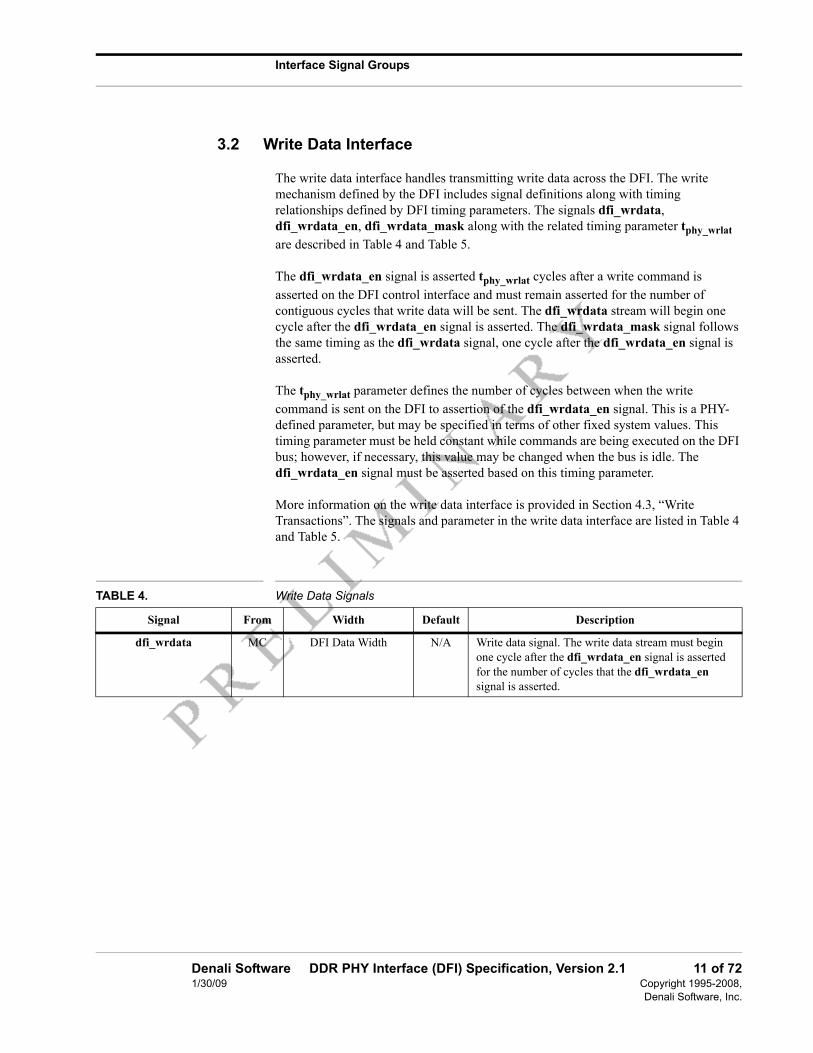
3.2 Write Data Interface
The write data interface handles transmitting write data across the DFI. The write mechanism defined by the DFI includes signal definitions along with timing relationships defined by DFI timing parameters. The signals dfi_wrdata, dfi_wrdata_en, dfi_wrdata_mask along with the related timing parameter tphy_wrlat
are described in Table 4 and Table 5.
The dfi_wrdata_en signal is asserted tphy_wrlat cycles after a write command is
asserted on the DFI control interface and must remain asserted for the number of contiguous cycles that write data will be sent. The dfi_wrdata stream will begin one cycle after the dfi_wrdata_en signal is asserted. The dfi_wrdata_mask signal follows the same timing as the dfi_wrdata signal, one cycle after the dfi_wrdata_en signal is asserted.
The tphy_wrlat parameter defines the number of cycles between when the write
command is sent on the DFI to assertion of the dfi_wrdata_en signal. This is a PHY-defined parameter, but may be specified in terms of other fixed system values. This timing parameter must be held constant while commands are being executed on the DFI bus; however, if necessary, this value may be changed when the bus is idle. The dfi_wrdata_en signal must be asserted based on this timing parameter.
More information on the write data interface is provided in Section 4.3, “Write Transactions”. The signals and parameter in the write data interface are listed in Table 4 and Table 5.
TABLE 4. Write Data Signals
Signal From Width Default Description
dfi_wrdata MC DFI Data Width N/A Write data signal. The write data stream must begin one cycle after the dfi_wrdata_en signal is asserted for the number of cycles that the dfi_wrdata_en signal is asserted.
Denali Software DDR PHY Interface (DFI) Specification, Version 2.1 11 of 721/30/09 Copyright 1995-2008,
Denali Software, Inc.

Interface Signal Groups
dfi_wrdata_en MC DFI Data Enable
Widtha0x0 Write data and data mask valid signals. These signals
must be asserted one cycle before the data and data mask are sent on the DFI interface. The dfi_wrdata_en signal must be sent tphy_wrlat cycles
after the write command.
Once the dfi_wrdata_en signal is asserted, it must remain asserted for the number of contiguous cycles of write data passed through the DFI write data interface.
The width of the dfi_wrdata_en signal is defined as a DFI term. Ideally, there will be a single dfi_wrdata_en bit for each slice of memory data. The dfi_wrdata_en [0] signal corresponds with the lowest segment of dfi_wrdata signals.
dfi_wrdata_mask MC DFI Data Width / 8 N/A Write data byte mask signal. The timing is the same as for the dfi_wrdata bus. The dfi_wrdata_mask [0] signal defines masking for the dfi_wrdata [7:0] signals, the dfi_wrdata_mask [1] signal defines masking for the dfi_wrdata [15:8] signals, etc. If the dfi_wrdata bus is not a multiple of 8, then the uppermost bit of the dfi_wrdata_mask signal corresponds to the most significant partial byte of data.
a. Since all bits of the dfi_wrdata_en signal are identical, the width of the signal on the MC side and the PHY side may be different; the PHY is not required to use all of the bits.
TABLE 5. Write Data Timing Parameter
ParameterDefined
By Min Max Unit Description
tphy_wrlat PHY 0 -a Cycles Specifies the number of DFI clocks between when a write command is sent on the DFI control interface and when the dfi_wrdata_en signal is asserted.
NOTE: This parameter may be specified as a fixed value, or as a constant based on other fixed values in the system.
a. The DFI does not specify a maximum value. The range of values supported is implementation-specific.
TABLE 4. Write Data Signals
Signal From Width Default Description
12 of 72 Denali Software DDR PHY Interface (DFI) Specification, Version 2.1Copyright 1995-2008, 1/30/09Denali Software, Inc.

Interface Signal Groups
3.3 Read Data Interface
The read data interface handles returning read data across the DFI. The read mechanism defined by the DFI includes signal definitions along with timing relationships defined by DFI timing parameters. The signals dfi_rddata, dfi_rddata_en, dfi_rddata_valid, the LPDDR2 signal dfi_rddata_dnv, along with the related timing parameters trddata_en and tphy_rdlat are described in Table 6 and Table 7.
The dfi_rddata_en signal is asserted trddata_en cycles after a read command is asserted
on the DFI control interface and must remain asserted for the number of contiguous cycles that read data is expected. Multiple read commands can be asserted on the DFI interface while the dfi_rddata_en signal is asserted. The dfi_rddata_en signal de-asserts to signify there is no more contiguous data expected from the DFI read command(s). Note that the dfi_rddata_en signal is not required to be asserted for any fixed number of cycles.
The trddata_en parameter defines the timing requirements between the read command on
the DFI interface and the assertion of the dfi_rddata_en signal at the DFI boundary for the start of contiguous read data expected on the DFI interface. The exact value of this parameter for a particular application is determined by the components in the entire DRAM system. The DFI specification does not dictate a value but does require that once this value has been determined, the dfi_rddata_en signal must be asserted based on this timing parameter.
The tphy_rdlat parameter defines the maximum number of cycles allowed from the
assertion of the dfi_rddata_en signal to the assertion of the dfi_rddata_valid signal. This parameter is specified by the system, but the exact value of this parameter is not determined by the DFI specification. These timing parameters (trddata_en and tphy_rdlat)
must be held constant while commands are being executed on the DFI bus; however, if necessary, these values may be changed when the bus is idle. The two timing parameters trddata_en and tphy_rdlat work together to define a maximum number of cycles from the
assertion of a read command on the DFI control interface to the assertion of the dfi_rddata_valid signal, indicating the first valid data of the contiguous read data. Read data may be returned earlier by asserting the dfi_rddata_valid signal before tphy_rdlat cycles have expired. When the signal dfi_rddata_valid is asserted, the entire
DFI read data word must be valid. For the LPDDR2 DFI, the signal dfi_rddata_dnv must also be sent with the read data signal dfi_rddata when the dfi_rddata_valid signal is asserted.
Denali Software DDR PHY Interface (DFI) Specification, Version 2.1 13 of 721/30/09 Copyright 1995-2008,
Denali Software, Inc.

Interface Signal Groups
More information on the read data interface is provided in Section 4.4, “Read Transactions”. The signals and parameters in the read data interface are listed in Table 6 and Table 7.
TABLE 6. Read Data Signals
Signal From Width Default Description
dfi_rddata PHY DFI Data Width N/A Read data signal. Read data is expected to be received at the MC within tphy_rdlat cycles after the
dfi_rddata_en signal is asserted.
dfi_rddata_en MC DFI Data Enable
Widtha
a. Since all bits of the dfi_rddata_en signal are identical, the width of the signal on the MC side and the PHY side may be different; the PHY is not required to use all of the bits.
0x0 Read data enable signal. The dfi_rddata_en signal must be asserted trddata_en cycles after the assertion
of a read command on the DFI control interface and remains valid for the duration of contiguous read data expected on the dfi_rddata bus.
The width of the dfi_rddata_en signal is defined as a DFI term. Ideally, there will be a single dfi_rddata_en bit for each slice of memory data. The dfi_rddata_en [0] signal corresponds with the lowest segment of dfi_rddata signals.
dfi_rddata_valid PHY DFI Read Data Valid
Widthb
b. Since all bits of the dfi_rddata_valid signal are identical, the width of the signal on the MC side and the PHY side may be different; the MC is not required to use all of the bits.
0x0 Read data valid indicator. The dfi_rddata_valid signal will be asserted with the read data for the number of cycles that data is being sent. The timing is the same as for the dfi_rddata bus.
dfi_rddata_dnv PHY DFI Data Width / 8 0x0 DFI data not valid signal. The timing is the same as for the dfi_rddata_valid signal.
The dfi_rddata_dnv [0] signal correlates to the dfi_rddata [7:0] signals, the dfi_rddata_dnv [1] signal correlates to the dfi_rddata [15:8] signals, etc. If the dfi_rddata bus is not a multiple of 8, then the uppermost bit of the dfi_rddata_dnv signal corresponds to the most significant partial byte of data.
This signal is only required for DFI LPDDR2 support.
14 of 72 Denali Software DDR PHY Interface (DFI) Specification, Version 2.1Copyright 1995-2008, 1/30/09Denali Software, Inc.

Interface Signal Groups
3.4 Update Interface
During system operation, the system may require updates to internal settings to compensate for environmental conditions. To ensure that updates do not interfere with signals on the DRAM interface, the DFI supports update modes where the DFI read, write, and control interface are suspended from normal activity. The DFI specification supports both MC-initiated and PHY-initiated updates. More information on the update interface is provided in Section 4.5, “PHY Update”.
If a MC initiates an update request by asserting the dfi_ctrlupd_req signal, the request can be acknowledged or ignored. If the request is acknowledged by asserting the dfi_ctrlupd_ack signal, the protocol described in Section 4.5.1, “MC-Initiated Update” must be followed. The DFI specification requires the MC to issue update requests and it specifies an interval in which requests must be offered. The MC should assert the dfi_ctrlupd_req signal at the end of memory initialization to signify that the initialization is complete.
If a PHY initiates an update request by asserting the dfi_phyupd_req signal, the request must be acknowledged through a dfi_phyupd_ack signal assertion. The DFI specifies up to 4 different update PHY-initiated request modes. Each mode differs only in the number of cycles that the DFI interface must be suspended while the update occurs. The MC is responsible for placing the system in a state where the DFI bus is suspended from all activity other than activity specifically related to the update process being executed. Refer to Section 4.5.2, “PHY-Initiated Update” for more details on this protocol. The DFI specification does not force the PHY to issue update requests nor does it specify an interval in which requests must be offered. If the PHY chooses to offer update requests, it must follow the specified protocol.
TABLE 7. Read Data Timing Parameters
ParameterDefined
By Min Max Unit Description
tphy_rdlat PHY 0 -a Cycles Specifies the maximum number of cycles allowed from the assertion of the dfi_rddata_en signal to the assertion of the dfi_rddata_valid signal.
NOTE: This parameter may be specified as a fixed value, or as a constant based on other fixed values in the system.
trddata_en System 0 -a Cycles Specifies the time from the assertion of a read command on the DFI to the assertion of the dfi_rddata_en signal.
NOTE: This parameter may be specified as a fixed value, or as a constant based on other fixed values in the system.
a. The DFI does not specify a maximum value. The range of values supported is implementation-specific.
Denali Software DDR PHY Interface (DFI) Specification, Version 2.1 15 of 721/30/09 Copyright 1995-2008,
Denali Software, Inc.

Interface Signal Groups
The signals and timing parameters in the update interface are listed in Table 8 and Table 9.
TABLE 8. Update Interface Signals
Signal From Width Default Description
dfi_ctrlupd_ack PHY 1 bit 0x0 The dfi_ctrlupd_ack signal is asserted to acknowledge a MC-initiated update request. The PHY is not required to acknowledge this request.
While this signal is asserted, the DFI bus must remain idle other than any transactions specifically associated with the update process.
If the PHY chooses to acknowledge the request, the dfi_ctrlupd_ack signal must be asserted before the dfi_ctrlupd_req signal de-asserts. If the PHY chooses to ignore the request, the dfi_ctrlupd_ack signal must remain de-asserted until the dfi_ctrlupd_req signal is de-asserted.
The dfi_ctrlupd_req signal is guaranteed to be asserted for at least tctrlupd_min cycles.
dfi_ctrlupd_req MC 1 bit 0x0 The dfi_ctrlupd_req signal is used with a MC-initiated update to indicate that the DFI will be idle for some time, in which the PHY may perform an update.
The dfi_ctrlupd_req signal must be asserted for a minimum of tctrlupd_min cycles and a maximum of
tctrlupd_max cycles.
A dfi_ctrlupd_req signal assertion is an invitation for the PHY to update and does not require a response.
The behavior of the dfi_ctrlupd_req signal is dependent on the dfi_ctrlupd_ack signal:
• If the update is acknowledged by the PHY, then the dfi_ctrlupd_req signal will remain asserted as long as the dfi_ctrlupd_ack signal asserted, but will de-assert before tctrlupd_max expires. While this signal is asserted, the DFI bus will remain idle other than any transactions specifically associated with the update process.
• If the update is not acknowledged, the dfi_ctrlupd_req signal may de-assert at any time after tctrlupd_min, and before tctrlupd_max.
16 of 72 Denali Software DDR PHY Interface (DFI) Specification, Version 2.1Copyright 1995-2008, 1/30/09Denali Software, Inc.

Interface Signal Groups
dfi_phyupd_ack MC 1 bit 0x0 The dfi_phyupd_ack signal is used for a PHY-initiated update to indicate that the DFI is idle and will remain so until the dfi_phyupd_req signal de-asserts.
The dfi_phyupd_ack signal must assert within tphyupd_resp cycles of the dfi_phyupd_req signal,
and must remain asserted as long as the dfi_phyupd_req signal remains asserted. The dfi_phyupd_ack signal must de-assert on the cycle following the dfi_phyupd_req signal de-assertion.
While this signal is asserted, the DFI bus must remain idle other than any transactions specifically associated with the update process.
The entire time period from when the dfi_phyupd_ack signal is asserted to when the dfi_phyupd_req signal is de-asserted will be a maximum of tphyupd_typeX cycles, based on the
dfi_phyupd_type signal.
dfi_phyupd_req PHY 1 bit 0x0 The dfi_phyupd_req signal is used for a PHY-initiated update to indicate that the PHY requires the DFI to not send control, read or write commands or data for a specified period of time. The maximum time required is specified by the tphyupd_typeX
parameter associated with the dfi_phyupd_type signal.
Once asserted, the dfi_phyupd_req signal must remain asserted until the request is acknowledged by the assertion of the dfi_phyupd_ack signal and the update has been completed.
While this signal is asserted, the DFI bus must remain idle other than any transactions specifically associated with the update process.
The de-assertion of the dfi_phyupd_req signal triggers the de-assertion of the dfi_phyupd_ack signal.
dfi_phyupd_type PHY 2 bits N/A The dfi_phyupd_type signal indicates which one of the 4 types of PHY update times is being requested by the dfi_phyupd_req signal. The value of the dfi_phyupd_type signal will determine which of the timing parameters (tphyupd_type0, tphyupd_type1,
tphyupd_type2, tphyupd_type3) is relevant. The
dfi_phyupd_type signal must remain constant during the entire time the dfi_phyupd_req signal is asserted.
TABLE 8. Update Interface Signals
Signal From Width Default Description
Denali Software DDR PHY Interface (DFI) Specification, Version 2.1 17 of 721/30/09 Copyright 1995-2008,
Denali Software, Inc.

Interface Signal Groups
TABLE 9. Update Timing Parameters
ParameterDefined
By Min Max Unit Description
tctrlupd_interval MC -a -b Cycles Specifies the maximum number of DFI clock cycles that the MC may wait between assertions of the dfi_ctrlupd_req signal.
tctrlupd_min MC 1 -b Cycles Specifies the minimum number of DFI clock cycles that the dfi_ctrlupd_req signal must be asserted.
tctrlupd_max MC -a -b Cycles Specifies the maximum number of DFI clock cycles that the dfi_ctrlupd_req signal can assert.
tphyupd_type0 PHY 1 -b Cycles Specifies the maximum number of DFI clock cycles that the dfi_phyupd_req signal may remain asserted after the assertion of the dfi_phyupd_ack signal for dfi_phyupd_type = 0x0. The dfi_phyupd_req signal may de-assert at any cycle after the assertion of the dfi_phyupd_ack signal.
tphyupd_type1 PHY 1 -b Cycles Specifies the maximum number of DFI clock cycles that the dfi_phyupd_req signal may remain asserted after the assertion of the dfi_phyupd_ack signal for dfi_phyupd_type = 0x1. The dfi_phyupd_req signal may de-assert at any cycle after the assertion of the dfi_phyupd_ack signal.
tphyupd_type2 PHY 1 -b Cycles Specifies the maximum number of DFI clock cycles that the dfi_phyupd_req signal may remain asserted after the assertion of the dfi_phyupd_ack signal for dfi_phyupd_type = 0x2. The dfi_phyupd_req signal may de-assert at any cycle after the assertion of the dfi_phyupd_ack signal.
tphyupd_type3 PHY 1 -b Cycles Specifies the maximum number of DFI clock cycles that the dfi_phyupd_req signal may remain asserted after the assertion of the dfi_phyupd_ack signal for dfi_phyupd_type = 0x3. The dfi_phyupd_req signal may de-assert at any cycle after the assertion of the dfi_phyupd_ack signal.
tphyupd_resp PHY 1 -b Cycles Specifies the maximum number of cycles after the assertion of the dfi_phyupd_req signal to the assertion of the dfi_phyupd_ack signal.
a. The DFI does not specify a minimum value. The range of values supported is an implementation-specific design parameter.
b. The DFI does not specify a maximum value. The range of values supported is an implementation-specific design parameter.
18 of 72 Denali Software DDR PHY Interface (DFI) Specification, Version 2.1Copyright 1995-2008, 1/30/09Denali Software, Inc.

Interface Signal Groups
3.5 Status Interface
The DFI requires status information for initialization and clock control to the DRAM devices. These signals are used to convey information between the MC and the PHY. An optional handshaking protocol is included in this interface.
The memory specifications define various memory states in which the clock frequency to the memory devices may be changed. When the memory is in an appropriate state, the MC may assert the dfi_init_start signal to the PHY indicating a clock frequency change request. The PHY can accept the clock frequency change request by de-asserting the dfi_init_complete signal. If the PHY does not de-assert the dfi_init_complete signal within tinit_start clock cycles, the dfi_init_start signal must be de-asserted and
the clock frequency change protocol will be aborted. If acknowledged, the clock frequency can be changed and, once the clock is operating at the new clock frequency, the MC will de-assert the dfi_init_start signal. When the PHY has re-initialized to the new clock frequency, it will respond by re-asserting the dfi_init_complete signal. During the clock frequency change, the DFI clock must maintain a valid clock operating frequency or be gated high or low.
More information on initialization is provided in Section 4.1, “Initialization”, more information on the clock disable interface is provided in Section 4.6, “DFI Clock Disabling” and more information on the frequency change protocol is provided in Section 4.8, “Frequency Changing”.
Denali Software DDR PHY Interface (DFI) Specification, Version 2.1 19 of 721/30/09 Copyright 1995-2008,
Denali Software, Inc.

Interface Signal Groups
The signals and timing parameters for the status interface are listed in Table 10 and Table 11.
TABLE 10. Status Interface Signals
Signal From Width Default Description
dfi_dram_clk_disable MC DFI Chip Select Width 0x0 DRAM clock disable signal. When active, this indicates to the PHY that the clocks to the DRAM devices must be disabled such that the clock signals hold a constant value. When the dfi_dram_clk_disable signal is inactive, the DRAMs should be clocked normally.
20 of 72 Denali Software DDR PHY Interface (DFI) Specification, Version 2.1Copyright 1995-2008, 1/30/09Denali Software, Inc.

Interface Signal Groups
dfi_init_complete PHY 1 bit 0x0 PHY initialization complete signal. The dfi_init_complete signal indicates that the PHY is able to respond to any proper stimulus on the DFI. All DFI signals must be held at their default values until the dfi_init_complete signal asserts. During a PHY re-initialization request (such a frequency change), this signal will be de-asserted. For a frequency change request, the de-assertion of the dfi_init_complete signal acknowledges the frequency change protocol. Once de-asserted, the signal should only be re-asserted within tinit_complete cycles after the
dfi_init_start signal has de-asserted, and once the PHY has completed re-initialization.
dfi_init_start MC 1 bit 0x0 DFI initialization start signal. When this signal is asserted, the MC is requesting a frequency change. This signal is optional and will only be relevant for MCs and PHYs that support the frequency change protocol.
A dfi_init_start signal assertion is an invitation for the PHY to accept frequency changing and does not require a response. However, if desired, the PHY must respond within tinit_start cycles, or the
opportunity for frequency change will be withdrawn until the MC re-asserts this signal.
The behavior of the dfi_init_start signal is dependent on the dfi_init_complete signal:
• If the PHY wishes to accept the frequency change request, it must de-assert the dfi_init_complete signal within tinit_start cycles of the dfi_init_start assertion. The MC will continue to hold the dfi_init_start signal asserted until the clock frequency change has been completed. The de-assertion should be used by the PHY to re-initialize on the new clock frequency.
• If the frequency change is not acknowledged (the dfi_init_complete signal remains asserted), the dfi_init_start signal must de-assert after tinit_start cycles.
TABLE 10. Status Interface Signals
Signal From Width Default Description
Denali Software DDR PHY Interface (DFI) Specification, Version 2.1 21 of 721/30/09 Copyright 1995-2008,
Denali Software, Inc.

Interface Signal Groups
3.6 Training Interface
DDR3 memories feature additional functions which allow for more accurate alignment of critical timing signals. The DFI specification accounts for these functions by providing a training interface.
The DFI specification supports read leveling and write leveling. The JEDEC specification requires these procedures to be performed independently with no other processes running simultaneously. Read leveling provides a method for data eye training and for gate training. More information on the training interface is provided in Section 4.9, “Training Operations - Read and Write Leveling”. The signals and timing parameters for the training interface are listed in Table 12 and Table 13.
Not all DFI training signals are used in all systems. Only the dfi_rdlvl_mode, dfi_wrlvl_mode and dfi_rdlvl_gate_mode signals are required for all PHYs and all MCs. These signals are used to indicate the type of read leveling, write leveling and gate training supported by the PHY: “No Support”, “MC Evaluation”, “PHY Evaluation” or “PHY Independent”. The MC must support all of the read and write leveling modes to be fully DFI-compliant; however, the PHY is expected to support only a single mode per training operation. The signals required for read leveling, write leveling and gate
TABLE 11. Status Timing Parameters
ParameterDefined
By Min Max Unit Description
tdram_clk_disable PHY 0 -a Cycles Specifies the number of clocks from the assertion of the dfi_dram_clk_disable signal on the DFI until the clock to the DRAM memory devices, at the PHY-DRAM boundary, maintains a low value.
NOTE: This parameter may be specified as a fixed value, or as a constant based on other fixed values in the system.
tdram_clk_enable PHY 0 -a Cycles Specifies the number of clocks from the de-assertion of the dfi_dram_clk_disable signal on the DFI until the first valid rising edge of the clock to the DRAM memory devices, at the PHY-DRAM boundary.
NOTE: This parameter may be specified as a fixed value, or as a constant based on other fixed values in the system.
tinit_start MC 0 -a Cycles Specifies the number of DFI clocks from the assertion of the dfi_init_start signal on the DFI until the PHY must respond by de-assert-ing the dfi_init_complete signal. If the dfi_init_complete signal is not de-asserted within this time period, the PHY is indicating that it can not, or does not wish to, support the frequency change. At this point, the MC must abort the request and release the dfi_init_start signal. Once tinit_start
expires, the PHY must not de-assert the dfi_init_complete signal. The MC may re-assert dfi_init_start at a later point.
tinit_complete PHY 0 -a Cycles Specifies the maximum number of cycles after the de-assertion of the dfi_init_start signal to the re-assertion of the dfi_init_complete signal.
a. The DFI does not specify a maximum value. The range of values supported is an implementation-specific design parameter.
22 of 72 Denali Software DDR PHY Interface (DFI) Specification, Version 2.1Copyright 1995-2008, 1/30/09Denali Software, Inc.

Interface Signal Groups
training must be limited to the signals defined in this specification. The signal set for the training interface is mode-dependent and the relevance of each signal is indicated in the descriptions.
For “PHY Evaluation” mode, it is possible to perform both data eye training and gate training using just the read leveling signals since these operations result in identical sequences for the MC. However, a separate set of signals is provided for gate training for “MC Evaluation” mode and may be used for gate training by a PHY operating in “PHY Evaluation” mode if desired.
The read and write leveling signals that communicate from the MC to the PHY are internally fanned out inside the MC to allow a direct connection from the MC to each PHY memory data slice. Other than the delay signals (dfi_rdlvl_delay_X, dfi_rdlvl_gate_delay_X and dfi_wrlvl_delay_X), all of these fanout signals originating from the MC to the PHY must be driven with the same value. The read and
Denali Software DDR PHY Interface (DFI) Specification, Version 2.1 23 of 721/30/09 Copyright 1995-2008,
Denali Software, Inc.

Interface Signal Groups
write leveling signals that communicate from the PHY to the MC may be individually driven by each memory data slice or collectively driven as a single signal.
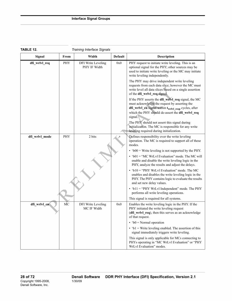
TABLE 12. Training Interface Signals
Signal From Width Default Description
dfi_rdlvl_req PHY DFI Read Leveling PHY IF Width
0x0 PHY request to initiate read leveling. This is an optional signal for the PHY; other sources may be used to initiate read leveling or the MC may initiate read leveling independently.
The PHY may drive independent read leveling requests from each data slice; however the MC must read level all data slices based on a single assertion of the dfi_rdlvl_req signal.
If the PHY asserts the dfi_rdlvl_req signal, the MC must acknowledge the request by asserting the dfi_rdlvl_en signal within trdlvl_resp cycles, after
which the PHY should de-assert the dfi_rdlvl_req signal.
The PHY should not assert this signal during initialization. The MC is responsible for any read leveling required during initialization.
dfi_rdlvl_gate_req PHY DFI Read Leveling PHY IF Width
0x0 PHY request to initiate gate training. This is an optional signal for the PHY; other sources may be used to initiate gate training or the MC may initiate gate training independently.
The PHY may drive independent gate training requests from each data slice; however the MC must gate train all data slices based on a single assertion of the dfi_rdlvl_gate_req signal.
If the PHY asserts the dfi_rdlvl_gate_req signal, the MC must acknowledge the request by asserting the dfi_rdlvl_gate_en signal within trdlvl_resp cycles,
after which the PHY should de-assert the dfi_rdlvl_gate_req signal.
The PHY should not assert this signal during initialization. The MC is responsible for any gate training required during initialization.
This signal is only applicable for MCs connecting to PHYs operating in “MC RdLvl Evaluation” mode.
24 of 72 Denali Software DDR PHY Interface (DFI) Specification, Version 2.1Copyright 1995-2008, 1/30/09Denali Software, Inc.

Interface Signal Groups
dfi_rdlvl_mode PHY 2 bits -a Defines responsibility over the read leveling operation. The MC is required to support all of these modes.
• ‘b00 = Read leveling is not supported by the PHY.
• ‘b01 = “MC RdLvl Evaluation” mode. The MC will enable and disable the read leveling logic in the PHY, analyze the results and adjust the delays.
• ‘b10 = “PHY RdLvl Evaluation” mode. The MC enables and disables the read leveling logic in the PHY. The PHY contains logic to evaluate the results and set new delay values.
• ‘b11 = “PHY RdLvl Independent” mode. The PHY performs all read leveling operations.
This signal is required for all systems.
dfi_rdlvl_gate_mode PHY 2 bits -a Defines responsibility over the gate training operation. The MC is required to support all of these modes.
• ‘b00 = Gate training is not supported by the PHY.
• ‘b01 = “MC RdLvl Evaluation” mode. The MC will enable and disable the gate training logic in the PHY, analyze the results and adjust the delays.
• ‘b10 = “PHY RdLvl Evaluation” mode. The MC enables and disables the gate training logic in the PHY. The PHY contains logic to evaluate the results and set new delay values.
• ‘b11 = “PHY RdLvl Independent” mode. The PHY performs all read leveling operations.
This signal is required for all systems.
dfi_rdlvl_en MC DFI Read Leveling MC IF Width
0x0 Enables the read leveling logic in the PHY. If the PHY initiated the read leveling request (dfi_rdlvl_req), then this serves as an acknowledge of that request.
• ‘b0 = Normal operation
• ‘b1 = Read leveling logic enabled. The assertion of this signal immediately triggers read leveling.
This signal is only applicable for MCs connecting to PHYs operating in “MC RdLvl Evaluation” or “PHY RdLvl Evaluation” modes.
TABLE 12. Training Interface Signals
Signal From Width Default Description
Denali Software DDR PHY Interface (DFI) Specification, Version 2.1 25 of 721/30/09 Copyright 1995-2008,
Denali Software, Inc.

Interface Signal Groups
dfi_rdlvl_gate_en MC DFI Read Leveling MC IF Width
0x0 Enables the gate training logic in the PHY. If the PHY initiated the gate training request (dfi_rdlvl_gate_req), then this serves as an acknowledge of that request.
• ‘b0 = Normal operation
• ‘b1 = Gate training logic enabled. The assertion of this signal immediately triggers gate training.
This signal is only applicable for MCs connecting to PHYs operating in “MC RdLvl Evaluation” or “PHY RdLvl Evaluation” modes.
dfi_rdlvl_cs_n MC DFI Chip Select Width 0x1 Indicates which chip select is currently active for read leveling.
This signal is only applicable for MCs connecting to PHYs operating in “MC RdLvl Evaluation” or “PHY RdLvl Evaluation” modes.
dfi_rdlvl_edge MC 1 bit 0x0 Indicates which edge of the read DQS is currently being used for the read leveling sequence. This signal must remain constant throughout the sequence. It is not a requirement to support read leveling of both the positive and negative edges of the read DQS.
• ‘b0 = Positive edge
• ‘b1 = Negative edge
This signal is only applicable for MCs connecting to PHYs operating in “MC RdLvl Evaluation” or “PHY RdLvl Evaluation” modes.
dfi_rdlvl_delay_X MC DFI Read Leveling Delay Width
0x0 Read leveling data delay. Indicates the programming of the delay in the PHY of the read DQS sampling read data. The width of the dfi_rdlvl_delay_X signals is defined as a DFI term.
In general, each memory data slice will be uniquely leveled and therefore a separate dfi_rdlvl_delay_X signal should be sent to each memory data slice X where dfi_rdlvl_delay_0 corresponds to the first data slice. In some applications, the PHY may only use a subset of the delay signals provided by the MC.
The width of each dfi_rdlvl_delay_X signal is defined by the programmability of the delay line.
This signal is only applicable for MCs connecting to PHYs operating in “MC RdLvl Evaluation” mode.
TABLE 12. Training Interface Signals
Signal From Width Default Description
26 of 72 Denali Software DDR PHY Interface (DFI) Specification, Version 2.1Copyright 1995-2008, 1/30/09Denali Software, Inc.

Interface Signal Groups
dfi_rdlvl_gate_delay_X MC DFI Read Leveling Gate Delay Width
0x0 Read leveling gate delay. Indicates the programming of the delay in the PHY of the gate sampling read data. The width of the dfi_rdlvl_gate_delay_X signals is defined as a DFI term.
In general, each memory data slice will be uniquely leveled and therefore a separate dfi_rdlvl_gate_delay_X signal should be sent to each memory data slice X where dfi_rdlvl_gate_delay_0 corresponds to the first data slice. In some applications, the PHY may only use a subset of the delay signals provided by the MC.
The width of each dfi_rdlvl_gate_delay_X signal is defined by the programmability of the delay line.
This signal is only applicable for MCs connecting to PHYs operating in “MC RdLvl Evaluation” mode.
dfi_rdlvl_load MC DFI Read Leveling MC IF Width
0x0 Read leveling load. The MC must send a one-cycle pulse on this signal when it has updated any of the delay times (dfi_rdlvl_delay_X or dfi_rdlvl_gate_delay_X) for the next read leveling command. This signal is only applicable for MCs connecting to PHYs operating in “MC RdLvl Evaluation” mode.
dfi_rdlvl_resp PHY DFI Read Leveling Response Width
0x0 Read leveling response. Response definition depends on the mode of operation:
• “PHY RdLvl Evaluation” mode: The response indicates that the PHY has completed read leveling and centered the DQS relative to the data.
• “MC RdLvl Evaluation” mode: The response indicates the sampled level of DQ or the value of read DQS gate. This value is used by the MC to determine how to adjust the delay value.
The width of the dfi_rdlvl_resp signal is defined as a DFI term. The width will generally be defined as a bit per memory data slice, or as the same width as the memory data bus. If the response width is the same as the memory data bus width, then the response for gate training should be sent on the lowest bit of each data slice.
This signal is only applicable for MCs connecting to PHYs operating in “MC RdLvl Evaluation” or “PHY RdLvl Evaluation” modes.
TABLE 12. Training Interface Signals
Signal From Width Default Description
Denali Software DDR PHY Interface (DFI) Specification, Version 2.1 27 of 721/30/09 Copyright 1995-2008,
Denali Software, Inc.
Interface Signal Groups
dfi_wrlvl_req PHY DFI Write Leveling PHY IF Width
0x0 PHY request to initiate write leveling. This is an optional signal for the PHY; other sources may be used to initiate write leveling or the MC may initiate write leveling independently.
The PHY may drive independent write leveling requests from each data slice; however the MC must write level all data slices based on a single assertion of the dfi_wrlvl_req signal.
If the PHY asserts the dfi_wrlvl_req signal, the MC must acknowledge the request by asserting the dfi_wrlvl_en signal within twrlvl_resp cycles, after
which the PHY should de-assert the dfi_wrlvl_req signal.
The PHY should not assert this signal during initialization. The MC is responsible for any write leveling required during initialization.
dfi_wrlvl_mode PHY 2 bits -a Defines responsibility over the write leveling operation. The MC is required to support all of these modes.
• ‘b00 = Write leveling is not supported by the PHY.
• ‘b01 = “MC WrLvl Evaluation” mode. The MC will enable and disable the write leveling logic in the PHY, analyze the results and adjust the delays.
• ‘b10 = “PHY WrLvl Evaluation” mode. The MC enables and disables the write leveling logic in the PHY. The PHY contains logic to evaluate the results and set new delay values.
• ‘b11 = “PHY WrLvl Independent” mode. The PHY performs all write leveling operations.
This signal is required for all systems.
dfi_wrlvl_en MC DFI Write Leveling MC IF Width
0x0 Enables the write leveling logic in the PHY. If the PHY initiated the write leveling request (dfi_wrlvl_req), then this serves as an acknowledge of that request.
• ‘b0 = Normal operation
• ‘b1 = Write leveling enabled. The assertion of this signal immediately triggers write leveling.
This signal is only applicable for MCs connecting to PHYs operating in “MC WrLvl Evaluation” or “PHY WrLvl Evaluation” modes.
TABLE 12. Training Interface Signals
Signal From Width Default Description
28 of 72 Denali Software DDR PHY Interface (DFI) Specification, Version 2.1Copyright 1995-2008, 1/30/09Denali Software, Inc.

Interface Signal Groups
dfi_wrlvl_cs_n MC DFI Chip Select Width 0x1 Indicates which chip select is currently active for write leveling.
This signal is only applicable for MCs connecting to PHYs operating in “MC WrLvl Evaluation” or “PHY WrLvl Evaluation” modes.
dfi_wrlvl_delay_X MC DFI Write Leveling Delay Width
0x0 Write leveling data delay. Indicates the programming of the delay in the PHY of the write DQS. The width of the dfi_wrlvl_delay_X signals is defined as a DFI term.
In general, each memory data slice will be uniquely leveled and therefore the MC should provide a separate dfi_wrlvl_delay_X signal for each memory data slice X where dfi_wrlvl_delay_0 corresponds to the first data slice.
The width of each dfi_wrlvl_delay_X signal is defined by the programmability of the delay line. In some applications, the PHY may only use a subset of the delay signals provided by the MC.
This signal is only applicable for MCs connecting to PHYs operating in “MC WrLvl Evaluation” mode.
dfi_wrlvl_load MC DFI Write Leveling MC IF Width
0x0 Write leveling load. The MC must send a 1 cycle pulse on this signal when it has updated any of the delay times (dfi_wrlvl_delay_X) for the next write leveling command. This signal is only applicable for MCs connecting to PHYs operating in “MC WrLvl Evaluation” mode.
TABLE 12. Training Interface Signals
Signal From Width Default Description
Denali Software DDR PHY Interface (DFI) Specification, Version 2.1 29 of 721/30/09 Copyright 1995-2008,
Denali Software, Inc.

Interface Signal Groups
Timing parameters are relevant for certain PHY Read and Write leveling modes and are identified accordingly in Table 13, “Training Interface Timing Parameters”. All timing parameters are defined only once for the interface and must apply to all PHY memory data slices.
dfi_wrlvl_strobe MC DFI Write Leveling MC IF Width
0x0 Triggers the PHY write leveling strobe.
This signal is only applicable for MCs connecting to PHYs operating in “MC WrLvl Evaluation” or “PHY WrLvl Evaluation” modes.
dfi_wrlvl_resp PHY DFI Write Leveling Response Width
0x0 Write leveling response. Response definition depends on the mode of operation:
• “PHY WrLvl Evaluation” mode: The response indicates that the PHY has completed write leveling and aligned the DQS relative to the memory clock.
• “MC WrLvl Evaluation” mode: The response indicates the sampled level of DQ. This value is used by the MC to determine how to adjust the delay value.
The width of the dfi_wrlvl_resp signal is defined as a DFI term. The width will generally be defined as a bit per memory data slice, or as the same width as the data bus.
This signal is only applicable for MCs connecting to PHYs operating in “MC WrLvl Evaluation” or “PHY WrLvl Evaluation” modes.
a. The default value is defined by the PHY implementation.
TABLE 13. Training Interface Timing Parameters
ParameterDefined
By Min Max Unit Description
trdlvl_dll PHY 1 -a DFI Clocks
Read leveling DLL delay. Specifies the minimum delay from when the MC asserts the dfi_rdlvl_load signal and updates the DLL delay in the appropriate dfi_rdlvl_delay_X or dfi_rdlvl_gate_delay_X signal to when the PHY is ready for the next read command.
This timing parameter is only applicable for MCs connecting to PHYs operating in “MC RdLvl Evaluation” mode.
trdlvl_en MC 1 -a DFI Clocks
Read leveling enable time. Specifies the minimum delay from the assertion of the dfi_rdlvl_en or dfi_rdlvl_gate_en signal to the first dfi_rdlvl_load signal assertion.
This timing parameter is only applicable for MCs connecting to PHYs operating in “MC RdLvl Evaluation” mode.
TABLE 12. Training Interface Signals
Signal From Width Default Description
30 of 72 Denali Software DDR PHY Interface (DFI) Specification, Version 2.1Copyright 1995-2008, 1/30/09Denali Software, Inc.

Interface Signal Groups
trdlvl_load MC 1 -a DFI Clocks
Read leveling delay settling time. Specifies the minimum number of cycles from when the delays are loaded on the dfi_rdlvl_delay_X or dfi_rdlvl_gate_delay_X signals to when the dfi_rdlvl_load signal may be asserted.
This timing parameter is only applicable for MCs connecting to PHYs operating in “MC RdLvl Evaluation” mode.
trdlvl_max MC -b -a DFI Clocks
Read leveling maximum time. Specifies the maximum number of DFI clock cycles that the MC will wait for a response (dfi_rdlvl_resp) to a read leveling enable signal (dfi_rdlvl_en or dfi_rdlvl_gate_en).
This timing parameter is only applicable for MCs connecting to PHYs operating in “PHY RdLvl Evaluation” mode.
trdlvl_resp MC 1 -a DFI Clocks
Read leveling response. Specifies the maximum number of DFI clock cycles after a read leveling request is asserted (dfi_rdlvl_req or dfi_rdlvl_gate_req) to when the MC will respond with a read leveling enable signal (dfi_rdlvl_en or dfi_rdlvl_gate_en).
trdlvl_resplat PHY 1 -a DFI Clocks
Read leveling response latency. Specifies the maximum number of cycles from the assertion of a read command to the guaranteed validity of the dfi_rdlvl_resp signal.
This timing parameter is only applicable for MCs connecting to PHYs operating in “MC RdLvl Evaluation” mode.
trdlvl_rr PHY -b -a DFI Clocks
Read leveling read-to-read delay. Specifies the minimum number of cycles after the assertion of a read command to the next read command.
This timing parameter is only applicable for MCs connecting to PHYs operating in “MC RdLvl Evaluation” or “PHY RdLvl Evaluation” modes.
twrlvl_dll PHY 1 -a DFI Clocks
Write leveling DLL delay. Specifies the minimum delay from when the MC asserts the dfi_wrlvl_load signal and updates the DLL delay in the appropriate dfi_wrlvl_delay_X signal to when the PHY is ready for the next dfi_wrlvl_strobe signal assertion.
This timing parameter is only applicable for MCs connecting to PHYs operating in “MC WrLvl Evaluation” mode.
twrlvl_en MC 1 -a DFI Clocks
Write leveling enable time. Specifies the minimum delay from the assertion of the dfi_wrlvl_en signal to the first dfi_wrlvl_load signal assertion.
This timing parameter is only applicable for MCs connecting to PHYs operating in “MC WrLvl Evaluation” mode.
twrlvl_load MC 1 -a DFI Clocks
Write leveling delay settling time. Specifies the minimum number of cycles from when the delays are loaded on the dfi_wrlvl_delay_X signals to when the dfi_wrlvl_load signal may be asserted.
This timing parameter is only applicable for MCs connecting to PHYs operating in “MC WrLvl Evaluation” mode.
TABLE 13. Training Interface Timing Parameters
ParameterDefined
By Min Max Unit Description
Denali Software DDR PHY Interface (DFI) Specification, Version 2.1 31 of 721/30/09 Copyright 1995-2008,
Denali Software, Inc.

Interface Signal Groups
twrlvl_max MC -b -a DFI Clocks
Write leveling maximum time. Specifies the maximum number of DFI clock cycles that the MC will wait for a response (dfi_wrlvl_resp) to a write leveling enable signal (dfi_wrlvl_en).
This timing parameter is only applicable for MCs connecting to PHYs operating in “PHY WrLvl Evaluation” mode.
twrlvl_resp MC 1 -a DFI Clocks
Write leveling response. Specifies the maximum number of DFI clock cycles after a write leveling request is asserted (dfi_wrlvl_req) to when the MC will respond with a write leveling enable signal (dfi_wrlvl_en).
twrlvl_resplat PHY 1 -a DFI Clocks
Write leveling response latency. Specifies the maximum number of cycles from the assertion of dfi_wrlvl_strobe signal to the guaranteed validity of the dfi_wrlvl_resp.
This timing parameter is only applicable for MCs connecting to PHYs operating in “MC WrLvl Evaluation” mode.
twrlvl_ww PHY -b -a DFI Clocks
Write leveling write-to-write delay. Specifies the minimum number of cycles after the assertion of the dfi_wrlvl_strobe signal to the next dfi_wrlvl_strobe signal assertion.
This timing parameter is only applicable for MCs connecting to PHYs operating in “MC WrLvl Evaluation” or “PHY WrLvl Evaluation” modes.
a. The DFI does not specify a maximum value. The range of values supported is an implementation-specific design parameter.
b. The DFI does not specify a minimum value. The range of values supported is an implementation-specific design parameter.
TABLE 13. Training Interface Timing Parameters
ParameterDefined
By Min Max Unit Description
32 of 72 Denali Software DDR PHY Interface (DFI) Specification, Version 2.1Copyright 1995-2008, 1/30/09Denali Software, Inc.

Functional Use
4.0 Functional Use
4.1 Initialization
For all DFI signals, the DFI specification requires that, as long as the dfi_init_complete signal is not asserted, the DFI signals must remain at default value. As shown in Figure 2, “Dependency on dfi_init_complete”, once the dfi_init_complete signal is asserted, all other DFI signals are able to assert in accordance with the DFI specification.
FIGURE 2. Dependency on dfi_init_complete
The DFI specification does not impose or dictate a reset sequence for either the PHY or the MC. However, the assertion of the dfi_init_complete signal signifies that the PHY is ready to respond to any assertions on the DFI by the MC. This does not ensure data integrity to the DRAMs, only that the PHY can respond to the changes with appropriate responses on the DFI. The PHY must guarantee the integrity of the address and control
dfi_address NOP
dfi_init_complete
dfi_reset_n
DFI clock
dfi_cke
dfi_cs_n
dfi_ras_n
dfi_cas_n
dfi_we_n
dfi_odt
dfi_wrdata_en
dfi_rddata_en
dfi_rddata_valid
dfi_dram_clk_disable
dfi_ctrlupd_ack
dfi_ctrlupd_req
dfi_phyupd_ack
dfi_phyupd_req
dfi_phyupd_type
Denali Software DDR PHY Interface (DFI) Specification, Version 2.1 33 of 721/30/09 Copyright 1995-2008,
Denali Software, Inc.

Functional Use
interface to the DRAMs prior to asserting the dfi_init_complete signal. Note that the DFI does not impose nor dictate any need for any type of signal training prior to DFI signal assertion. For LPDDR2 memories, the dfi_address bus must drive a NOP command until the dfi_init_complete signal is asserted and the signals dfi_bank, dfi_cas_n, dfi_ras_n and dfi_we_n are unused and must remain at a constant value when the DFI bus is being used.
The training interface signals similarly must remain at default until after the assertion of the dfi_init_complete signal.
4.2 Control Signals
The DFI control signals dfi_address, dfi_bank, dfi_cas_n, dfi_cke, dfi_cs_n, dfi_reset_n, dfi_odt, dfi_ras_n and dfi_we_n correlate to the DRAM control signals. For more information on these signals, refer to Section 3.1, “Control Interface”.
These control signals are expected to be driven to the memory devices. The DFI relationship of the control signals is expected to be maintained at the PHY-DRAM boundary; meaning that any delays should be consistent across all signals and is defined through the timing parameter tctrl_delay. Refer to Figure 3, “DFI Control Interface
Signal Relationships” for a graphical representation.
34 of 72 Denali Software DDR PHY Interface (DFI) Specification, Version 2.1Copyright 1995-2008, 1/30/09Denali Software, Inc.

Functional Use
FIGURE 3. DFI Control Interface Signal Relationships
The system may not be using all of the pins on the DRAM interface such as additional banks, chip selects, etc.; However, these signals must still be driven through the DFI and may not be left floating.
tctrl_delay
DFI clock
dfi_cke
dfi_cs_n
dfi_ras_na
dfi_cas_na
dfi_we_na
dfi_address
dfi_banka
dfi_odt
dfi_reset_n
WE_n
ADDRESS
CKE
CS_n
RAS_n
CAS_n
BANK
ODT
RESET_n
a) For LPDDR2, these signals are not used and should be held in an idle state.
Denali Software DDR PHY Interface (DFI) Specification, Version 2.1 35 of 721/30/09 Copyright 1995-2008,
Denali Software, Inc.

Functional Use
4.3 Write Transactions
The write transaction interface of the DFI includes the write data (dfi_wrdata), write data mask (dfi_wrdata_mask), and write data enable (dfi_wrdata_en) signals as well as the tphy_wrlat parameter. For more information on these signals, refer to Section 3.2,
“Write Data Interface”.
The dfi_wrdata_en signal must be asserted tphy_wrlat cycles after the assertion of the
corresponding write command on the DFI, and the dfi_wrdata_en signal must be asserted for the number of cycles required to complete the write data transfer sent on the DFI control interface. For contiguous write commands, the dfi_wrdata_en signal will be asserted tphy_wrlat cycles after the first write command of the stream and remain
asserted for the entire length of the data stream.
The associated write data (dfi_wrdata) and masking (dfi_wrdata_mask) is valid one cycle after the assertion of the dfi_wrdata_en signal on the DFI. The dfi_wrdata_en signal must de-assert on the cycle before the last valid data is transferred on the dfi_wrdata bus.
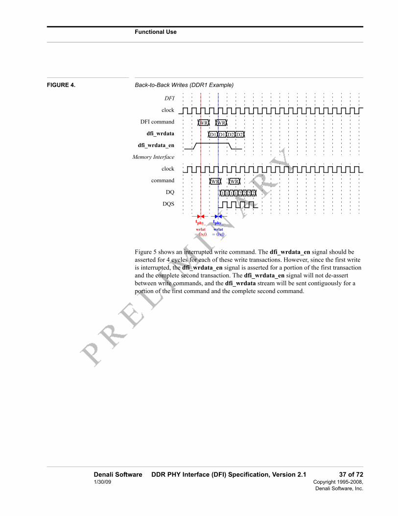
Six situations are presented in Figure 4, Figure 5, Figure 6, Figure 7, Figure 8 and Figure 9. All six situations show system behavior with two write transactions.
Figure 4, shows back-to-back writes for a system with a tphy_wrlat of zero. The
dfi_wrdata_en signal is asserted with the write command for this situation, and is asserted for two cycles per command to inform the DFI that two cycles of DFI data will be sent for each write command. The timing parameters and the timing of the write commands allow the dfi_wrdata_en signal and the dfi_wrdata stream to be sent contiguously.
36 of 72 Denali Software DDR PHY Interface (DFI) Specification, Version 2.1Copyright 1995-2008, 1/30/09Denali Software, Inc.
Functional Use
FIGURE 4. Back-to-Back Writes (DDR1 Example)
Figure 5 shows an interrupted write command. The dfi_wrdata_en signal should be asserted for 4 cycles for each of these write transactions. However, since the first write is interrupted, the dfi_wrdata_en signal is asserted for a portion of the first transaction and the complete second transaction. The dfi_wrdata_en signal will not de-assert between write commands, and the dfi_wrdata stream will be sent contiguously for a portion of the first command and the complete second command.
WR
1
tphy_
wrlat
DFI
clock
DFI command
dfi_wrdata
dfi_wrdata_en
Memory Interface
clock
command
DQ
DQS
WR
D1 D1 D2 D2
WR WR
1 1 1 22 2 2
= 0x0
tphy_
wrlat= 0x0
Denali Software DDR PHY Interface (DFI) Specification, Version 2.1 37 of 721/30/09 Copyright 1995-2008,
Denali Software, Inc.

Functional Use
FIGURE 5. Back-to-Back Interrupted Contiguous Writes (DDR2 Example)
Figure 6 shows back-to-back burst-of-8 writes. The dfi_wrdata_en signal must be asserted for 4 cycles for each of these write transactions.
FIGURE 6. Back-to-Back Writes (DDR3 Example)
tphy_wrlat
WR WR
2 2 2 2 22 2 2
DFI
clock
DFI command
dfi_wrdata
dfi_wrdata_en
Memory Interface
clock
command
DQ
DQS
WR WR
D1 D1 D2 D2 D2 D2
1 1 1 1
tphy_wrlat = 0x3
= 0x3
tphy_wrlat = 0x4
DFI
clock
DFI command
dfi_wrdata
dfi_wrdata_en
Memory Interface
clock
command
DQ
DQS
WR WR
D1 D1 D1 D1 D2 D2
WR WR
1 1 1 1 11 1 1
D2D2
2 2 2 22 2 22
38 of 72 Denali Software DDR PHY Interface (DFI) Specification, Version 2.1Copyright 1995-2008, 1/30/09Denali Software, Inc.

Functional Use
Figure 7, Figure 8, Figure 9 and Figure 10 also show two complete write commands, with different tphy_wrlat timing parameters and for different memory types. The
dfi_wrdata_en signal will be asserted for two cycles for each write transaction. The tphy_wrlat timing and the timing between the write commands causes the
dfi_wrdata_en signal to be de-asserted between commands. As a result, the dfi_wrdata stream will be non-contiguous.
FIGURE 7. Two Independent Writes (DDR1 Example)
WR WR
1 1 1 1 2 2 22
DFI
clock
DFI command
dfi_wrdata
dfi_wrdata_en
Memory Interface
clock
command
DQ
DQS
WR WR
D1 D1 D2 D2
tphy_wrlat
= 0x0
tphy_wrlat
= 0x0
Denali Software DDR PHY Interface (DFI) Specification, Version 2.1 39 of 721/30/09 Copyright 1995-2008,
Denali Software, Inc.

Functional Use
FIGURE 8. Two Independent Writes (DDR2 Example)
FIGURE 9. Two Independent Writes (DDR3 Example)
DFI
clock
DFI command
dfi_wrdata
dfi_wrdata_en
Memory Interface
clock
command
DQ
DQS
WR WR
D1 D1 D2 D2
WR WR
1 1 1 1 2 2 22
tphy_wrlattphy_wrlat
= 0x3= 0x3
DFI
clock
DFI command
dfi_wrdata
dfi_wrdata_en
Memory Interface
clock
command
DQ
DQS
WR WR
WR WR
D1 D1 D1 D1 D2 D2 D2D2
1 1 1 1 11 1 1 2 2 2 22 2 22
tphy_wrlat = 0x3
40 of 72 Denali Software DDR PHY Interface (DFI) Specification, Version 2.1Copyright 1995-2008, 1/30/09Denali Software, Inc.

Functional Use
FIGURE 10. Two Independent Writes (LPDDR2 Example)
4.4 Read Transactions
The read transaction portion of the DFI is defined by the read data enable (dfi_rddata_en), read data (dfi_rddata), the read data not valid for LPDDR2 memories (dfi_rddata_dnv) and the valid (dfi_rddata_valid) signals as well as the trddata_en and
tphy_rdlat timing parameters. For more information on these signals, refer to Section 3.3,
“Read Data Interface”.
For the DFI, the read data must be returned from the PHY within a maximum delay which is the sum of the trddata_en and tphy_rdlat timing parameters. The trddata_en is a
fixed delay, but the tphy_rdlat is defined as a maximum value. The delay can be adjusted
as long as both the MC and the PHY coordinate the change such that the DFI specification is still maintained. Both parameters may be expressed as equations based on other fixed system parameters.
The dfi_rddata_en signal must be asserted trddata_en cycles after the assertion of the
corresponding read command on the DFI, and the dfi_rddata_en signal must be asserted for the number of cycles of read data that the DFI is expecting. For contiguous read commands, the dfi_rddata_en signal will be asserted trddata_en cycles after the
first read command of the stream and remain asserted for the entire length of the data stream. The data will be returned, with the dfi_rddata_valid signal asserted, within tphy_rdlat cycles after the dfi_rddata_en signal for that command is asserted. For
LPDDR2 memories, the dfi_rddata_dnv signal has the same timing as the dfi_rddata signal.
DFI
clock
DFI command
dfi_wrdata
dfi_wrdata_en
Memory Interface
clock
Write commands
DQ
DQS
WR WR
D1 D1 D2 D2
1 1 1 1 2 2 22
tphy_wrlattphy_wrlat
= 0x3= 0x3
Denali Software DDR PHY Interface (DFI) Specification, Version 2.1 41 of 721/30/09 Copyright 1995-2008,
Denali Software, Inc.

Functional Use
Seven situations are presented in Figure 11, Figure 12, Figure 13, Figure 14, Figure 15, Figure 16 and Figure 17.
Figure 11 shows a single read transaction. In this case, the dfi_rddata_en signal is asserted for two cycles to inform the DFI that two cycles of DFI data are expected and data is returned tphy_rdlat cycles after the dfi_rddata_en signal assertion.
FIGURE 11. Single Read Transaction of 2 Data Words
Figure 12 shows a single read transaction where the data is returned in less than the maximum delay. The data returns one cycle less than the maximum PHY read latency.
FIGURE 12. Single Read Transaction of 4 Data Words
Figure 13 shows an interrupted read command. The dfi_rddata_en signal must be asserted for 4 cycles for each of these read transactions. However, since the first read is interrupted, the dfi_rddata_en signal is asserted for a portion of the first transaction and the complete second transaction. The dfi_rddata_en signal will not de-assert between read commands.
clock
DFI command
dfi_rddata_en
dfi_rddata_valid
dfi_rddata
RD
D1 D1
trddata_en = 0x4 tphy_rdlat = 0x5
clock
DFI command
dfi_rddata_en
dfi_rddata_valid
dfi_rddata
RD
D1 D1 D1 D1
trddata_en
= 0x4
tphy_rdlat
= 0x4
42 of 72 Denali Software DDR PHY Interface (DFI) Specification, Version 2.1Copyright 1995-2008, 1/30/09Denali Software, Inc.

Functional Use
FIGURE 13. Back-to-Back Read Transactions with First Read Burst Interrupted (DDR1 Example BL=8)
Figure 14 and Figure 15 also show two complete read transactions. The dfi_rddata_en signal will be asserted for two cycles for each read transaction. In Figure 14, the values for the timing parameters are such that the read data will be returned in a contiguous data stream for both transactions. Therefore, the dfi_rddata_en signal and the dfi_rddata_valid signal are each asserted for the complete read data stream.
FIGURE 14. Two Independent Read Transactions (DDR1 Example)
In Figure 15, the trddata_en timing and the timing between the read commands causes
the dfi_rddata_en signal to be de-asserted between commands. As a result, the dfi_rddata_valid signal will be de-asserted between commands and the dfi_rddata stream will be non-contiguous.
clock
DFI command
dfi_rddata_en
dfi_rddata_valid
dfi_rddata
RD1RD2
D1 D2 D2 D2 D2
trddata_en
= 0x3
tphy_rdlat
= 0x4
tphy_rdlat
= 0x4
trddata_en
= 0x3
tphy_rdlat
= 0x3
clock
DFI command
dfi_rddata_en
dfi_rddata_valid
dfi_rddata
RD1 RD2
D1 D1 D2 D2
trddata_en tphy_rdlat
= 0x2
= 0x3
trddata_en
= 0x2
Denali Software DDR PHY Interface (DFI) Specification, Version 2.1 43 of 721/30/09 Copyright 1995-2008,
Denali Software, Inc.
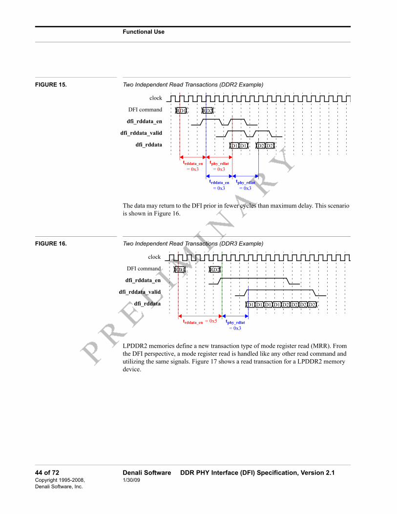
Functional Use
FIGURE 15. Two Independent Read Transactions (DDR2 Example)
The data may return to the DFI prior in fewer cycles than maximum delay. This scenario is shown in Figure 16.
FIGURE 16. Two Independent Read Transactions (DDR3 Example)
LPDDR2 memories define a new transaction type of mode register read (MRR). From the DFI perspective, a mode register read is handled like any other read command and utilizing the same signals. Figure 17 shows a read transaction for a LPDDR2 memory device.
clock
DFI command
dfi_rddata_en
dfi_rddata_valid
dfi_rddata
RD1 RD2
D1 D1 D2 D2
= 0x3
trddata_en tphy_rdlat
= 0x3
= 0x3
trddata_en tphy_rdlat
= 0x3
clock
DFI command
dfi_rddata_en
dfi_rddata_valid
dfi_rddata
RD1 RD2
D1 D1 D2 D2D1D1 D2 D2
trddata_en = 0x5 tphy_rdlat
= 0x3
44 of 72 Denali Software DDR PHY Interface (DFI) Specification, Version 2.1Copyright 1995-2008, 1/30/09Denali Software, Inc.

Functional Use
FIGURE 17. Example Read Transactions with LPDDR2
4.5 PHY Update
The DFI contains signals to support a MC-initiated and a PHY-initiated update process. The signals used in the update interface are: dfi_ctrlupd_req, dfi_ctrlupd_ack, dfi_phyupd_req, dfi_phyupd_type and dfi_phyupd_ack. For more information on these signals, refer to Section 3.4, “Update Interface”.
4.5.1 MC-Initiated Update
During normal operation, the MC may encounter idle time during which no commands are being issued to the memory devices and all outstanding read and write data have have been transferred on the DFI. Assertion of the dfi_ctrlupd_req signal indicates the control, read and write interfaces on the DFI are idle. While the dfi_ctrlupd_ack signal is asserted, the DFI bus may only be used for commands related to the update process.
The MC guarantees that dfi_ctrlupd_req signal will be asserted for at least tctrlupd_min
cycles, allowing the PHY time to respond. The PHY may respond or ignore the update request. To acknowledge the request, the dfi_ctrlupd_ack signal must be asserted while the dfi_ctrlupd_req signal is asserted. The dfi_ctrlupd_ack signal must de-assert at least one cycle before tctrlupd_max expires.
The MC must hold the dfi_ctrlupd_req signal as long as the dfi_ctrlupd_ack signal is asserted, and must de-assert the dfi_ctrlupd_req signal before tctrlupd_max expires.
Note that the number of cycles after the dfi_ctrlupd_ack signal de-asserts before the dfi_ctrlupd_req signal de-asserts is not specified by the DFI. This situation is shown in Figure 18.
clock
DFI command
dfi_rddata_en
dfi_rddata_valid
dfi_rddata
RD
D01
D23
00 0fdfi_rddata_dnv
trddata_en = 0x5 tphy_rdlat = 0x4
Denali Software DDR PHY Interface (DFI) Specification, Version 2.1 45 of 721/30/09 Copyright 1995-2008,
Denali Software, Inc.

Functional Use
FIGURE 18. MC-Initiated Update Timing Diagram
It is important to note that the dfi_ctrlupd_ack signal is not required to assert when the dfi_ctrlupd_req signal is asserted. The MC must assert the dfi_ctrlupd_req signal for at least tctrlupd_min within every tctrlupd_interval cycles, but the total number of cycles
that the dfi_ctrlupd_req signal is asserted must not exceed tctrlupd_max. This scenario
is shown in Figure 19.
FIGURE 19. MC-Initiated Update with No Response
4.5.2 PHY-Initiated Update
The PHY may also trigger the DFI into an idle state. This update process utilizes three signals: dfi_phyupd_req, dfi_phyupd_type and dfi_phyupd_ack. The dfi_phyupd_req signal indicates the need for idle time on the DFI, the dfi_phyupd_type signal defines the type of update required, and the dfi_phyupd_ack signal is the MC’s response signal. Four update types are specified by the DFI.
To request an update, the dfi_phyupd_type signal must be valid when the dfi_phyupd_req signal is asserted. The tphyupd_typeX parameters indicate the number
of cycles of idle time on the DFI control, read and write data interfaces being requested. The dfi_phyupd_ack signal must assert within tphyupd_resp cycles after the assertion of
the dfi_phyupd_req signal.
clock
dfi_ctrlupd_req
dfi_ctrlupd_ack
<=
tctrlupd_min
tctrlupd_min
tctrlupd_max<= assertion time <=
clock
dfi_ctrlupd_req
dfi_ctrlupd_ack
tctrlupd_min
tctrlupd_max
>=
<=
46 of 72 Denali Software DDR PHY Interface (DFI) Specification, Version 2.1Copyright 1995-2008, 1/30/09Denali Software, Inc.

Functional Use
When the dfi_phyupd_ack signal is asserted, it must remain asserted until the dfi_phyupd_req signal de-asserts or until tphyupd_typeX cycles have expired. The
dfi_phyupd_ack signal must de-assert one cycle after the de-assertion of the dfi_phyupd_req signal. While the dfi_phyupd_ack signal is asserted, the DFI bus may only be used for commands related to the update process.
Unlike MC-initiated updates, the MC must respond to a PHY update request as shown in Figure 20.
FIGURE 20. PHY-Initiated Update Timing Diagram
4.6 DFI Clock Disabling
The DFI contains a dfi_dram_clk_disable signal which controls the DRAM clock signal to the DRAM device(s). In the default state, the DRAM clock functions normally and the dfi_dram_clk_disable bits are all de-asserted. If the system requires the clocks of the memory device(s) to be disabled, then the dfi_dram_clk_disable signal will be asserted. For more information on the dfi_dram_clk_disable signal, refer to Section 3.5, “Status Interface”.
Two timing parameters tdram_clk_disable and tdram_clk_enable indicate the number of DFI
cycles that the PHY requires to respond to the assertion and de-assertion of the dfi_dram_clk_disable signal. The tdram_clk_disable value determines the number of
DFI cycles in which a rising edge of the dfi_dram_clk_disable signal affects the DRAM clock and tdram_clk_enable sets the number of cycles required for the DRAM
clock to be active again, as shown in Figure 21.
’b01
clock
dfi_phyupd_req
dfi_phyupd_type
dfi_phyupd_ack
tphyupd_typeXtphyupd_resp
<=<=
Denali Software DDR PHY Interface (DFI) Specification, Version 2.1 47 of 721/30/09 Copyright 1995-2008,
Denali Software, Inc.

Functional Use
FIGURE 21. DRAM Clock Disable Behavior
4.7 Frequency Ratios Across the DFI
In a DDR memory subsystem, it may be advantageous to operate the PHY at a higher frequency than the MC. If the PHY operates at a multiple of the MC frequency, the PHY transfers data at a higher data rate relative to the MC clock and may execute multiple commands in a single MC clock cycle. The DFI is defined as the PHY boundary and therefore operates in the higher clock frequency domain of the PHY.
The DFI specification does not define how frequency conversion should be handled. However, additional logic may be required on the MC side of the DFI to convert from the lower frequency MC clock domain to the higher frequency DFI clock domain. In addition, the MC may have multiple DFI buses connecting to frequency conversion logic which allows generation of multiple commands per MC clock to take advantage of the higher frequency of the PHY clock. If this is true, the frequency conversion logic will need to serialize the interface in the higher frequency clock domain.
Figure 22, “Example of Frequency Ratio Scaling” demonstrates a 1:4 MC:PHY clock ratio system. In this example, the DFI bus does not directly interface the MC and the PHY, however, the same protocol applies to either side of the frequency conversion logic block. Additional signalling may be required between the MC and the frequency conversion logic to account for the clock scaling of signals that communicate timing information such as dfi_rddata_en and dfi_wrdata_en. Any additional signals are specific to the implementation. For this example, the DFI bus segment between the frequency conversion logic and the PHY requires no additional signalling. The DFI clocks for the various bus segments should be even clock multiples and phase aligned. Although this example illustrates the frequency conversion logic as a separate block, the logic may be implemented as part of the MC, the PHY or as a separate module.
clock
dfi_dram_clk_disable
DRAM clock
tdram_clk_enabletdram_clk_disable
48 of 72 Denali Software DDR PHY Interface (DFI) Specification, Version 2.1Copyright 1995-2008, 1/30/09Denali Software, Inc.

Functional Use
FIGURE 22. Example of Frequency Ratio Scaling
The DFI buses interfacing the MC and the frequency logic should be sequenced in ascending order, sending lower bus segment control signals first, followed by higher bus segment signals. The read data interface should follow the same ordering convention to correlate the read data with the appropriate command. This allows the MC to properly account for memory clocks associated with cycle-to-cycle timing required by the DRAM specification.
Refer to Figure 23, “Frequency Ratio Write Example (2:1 Ratio)” and Figure 24, “Frequency Ratio Read Example (4:1 Ratio)” for graphical examples of frequency ratio systems using DFI.
Figure 23 shows a sequence in which the PHY is operating at twice the frequency of the MC. In this example implementation, the additional bus bandwidth provided by the higher-frequency memory interface is utilized by feeding two DFI buses into the frequency conversion logic. One bus is used to send a non-data command. Note that this is only one example configuration and that the DFI specification allows for different implementations to utilize the increased memory bus bandwidth.
NOTE: The read data and read data valid signal from memory must be clocked in the PHY at the frequency of the DFI bus connecting the PHY to the frequency conversion logic. The user may choose to register the read data on the MC clock frequency in the frequency conversion logic, but this is not required. Since this data is still sent from a register, DFI compliance is not compromised.
MCFrequency Conversion
LogicPHY
DFI Bus 0
Frequency Conversion Signalling
DFI Bus 1
DFI Bus
DFI Clock Frequency = 4X MC Clock Frequency
DFI Clock Frequency = MC Clock Frequency
Denali Software DDR PHY Interface (DFI) Specification, Version 2.1 49 of 721/30/09 Copyright 1995-2008,
Denali Software, Inc.

Functional Use
D2
AC
T
D2
D1
D1
D1
D1
WR
1W
R2
WR
1
AC
T
D1
D1
dfi
_wrd
ata
dfi
_wrd
ata_
en
DF
I C
omm
and
DF
I (P
HY
Clo
ck D
omai
n)
cloc
k
DF
I C
omm
and
DF
I bu
s 1
dfi
_wrd
ata_
en
dfi
_wrd
ata
DF
I C
omm
and
DF
I bu
s 0
DF
I (M
C C
lock
Dom
ain)
cloc
k
FIG
UR
E 2
3.
Fre
que
ncy
Rat
io W
rite
Exa
mp
le (
2:1
Rat
io)
D2
WR
2
D2
D2
D2
50 of 72 Denali Software DDR PHY Interface (DFI) Specification, Version 2.1Copyright 1995-2008, 1/30/09Denali Software, Inc.

Functional Use
Figure 24 shows a read command for a situation in which the PHY is operating at four times the frequency of the MC. In this implementation, there are still two DFI buses feeding into the frequency conversion logic.
The DFI specification does not specify the implementation of any non-matched frequency system. Figure 24 is only an example of one configuration.
Denali Software DDR PHY Interface (DFI) Specification, Version 2.1 51 of 721/30/09 Copyright 1995-2008,
Denali Software, Inc.
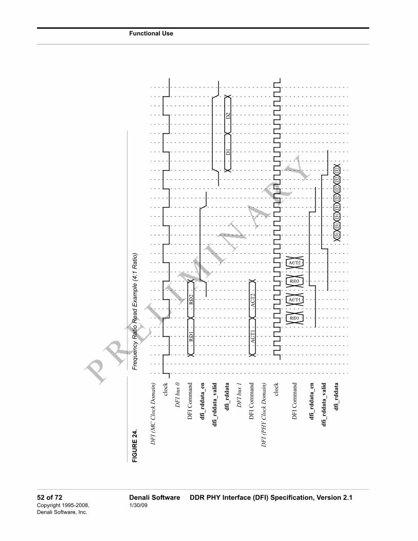
Functional Use
D2
D1
D1
D1
D1
D2
D2
D2
RD
1R
D2
ACT1
RD1
AC
T2
AC
T1
D2
D1
dfi
_rd
dat
a
dfi
_rd
dat
a_va
lid
dfi
_rd
dat
a_en
DF
I C
omm
and
DF
I (P
HY
Clo
ck D
omai
n)
cloc
k
DF
I C
omm
and
DF
I bu
s 1
dfi
_rd
dat
a
dfi
_rd
dat
a_va
lid
dfi
_rd
dat
a_en
DF
I C
omm
and
DF
I bu
s 0
DF
I (M
C C
lock
Dom
ain)
cloc
k
ACT2
RD2
FIG
UR
E 2
4.
Fre
que
ncy
Rat
io R
ead
Exa
mpl
e (
4:1
Rat
io)
52 of 72 Denali Software DDR PHY Interface (DFI) Specification, Version 2.1Copyright 1995-2008, 1/30/09Denali Software, Inc.

Functional Use
4.8 Frequency Changing
There are situations in which the system may wish to change the clock frequency of the memory controller and PHY without completely resetting the system. The memory specifications define various memory states in which the clock frequency can safely be changed. The general procedure is to put the memory in one of these states, modify the clock frequency and then re-synchronize the system. When the new clock frequency has been established, the PHY may need to re-initialize various circuits to the new clock frequency prior to resuming normal memory operation. Once complete, the memory system is ready to resume normal operation. The DFI specification defines a frequency change protocol between the MC and the PHY to allow the devices to coordinate this frequency change process.
This is an optional feature of the DFI 2.1 specification and is not required for DFI 2.1 compliance. The system may use a non-DFI frequency change method, or may choose to not support frequency change at all. However, if both the MC and the PHY intend to use the DFI 2.1 frequency change protocol, then they must comply with the handshaking defined by the specification. The handshaking protocol defines the signals through which the MC and the PHY will allow a frequency change to occur and also provides a means to abort the process if the PHY does not respond to a frequency change request. When a frequency change occurs, some of the DFI timing parameters may need to be changed.
NOTE: During the frequency change, the DFI clock must remain valid - either operating at a valid frequency or gated high or low.
The signals used in the frequency change protocol are dfi_init_start and dfi_init_complete. For more information on these signals, refer to Section 3.5, “Status Interface”.
4.8.1 Frequency Change Protocol - Acknowledged
During normal operation, the system may wish to change the DFI clock frequency. The MC asserts the dfi_init_start signal to indicate that a clock frequency change is being requested.
The MC guarantees that the dfi_init_start signal will remain asserted for at least tinit_start cycles, allowing the PHY time to respond. The PHY may respond or ignore
the frequency change request. To acknowledge the request, the dfi_init_complete signal must be de-asserted within tinit_start cycles of the assertion of the dfi_init_start
signal. The dfi_init_complete signal must de-assert at least one cycle before tinit_start
expires.
If the frequency change is acknowledged, the MC must hold the dfi_init_start signal asserted as long as the frequency change continues. Once the frequency change has completed, the MC will de-assert the dfi_init_start signal. The PHY must then complete any re-initialization required for the new clock frequency and re-assert dfi_init_complete within tdfi_init_complete cycles. This scenario is shown in Figure 25.
Denali Software DDR PHY Interface (DFI) Specification, Version 2.1 53 of 721/30/09 Copyright 1995-2008,
Denali Software, Inc.

Functional Use
Note that no maximum number of cycles for the entire cycle to complete is specified by the DFI.
FIGURE 25. Frequency Change Acknowledge Timing Diagram
4.8.2 Frequency Change Protocol - Not Acknowledged
It is important to note that the PHY is not required to respond to a frequency change request. The MC must assert the dfi_init_start signal for at least tinit_start cycles. This
scenario is shown in Figure 26.
FIGURE 26. Frequency Change Request Ignored Timing Diagram
4.9 Training Operations - Read and Write Leveling
The DFI contains a set of signals to support read and write leveling. The read leveling logic may be used to perform both data eye training and gate training.
4.9.1 Read Leveling
The goal of data eye training is to identify the delay at which the read DQS rising edge aligns with the beginning and end transitions of the associated DQ data eye. By identifying these delays, the system can calculate the midpoint between the delays and accurately center the read DQS within the DQ data eye.
The goal of gate training is to locate the delay at which the initial read DQS rising edge aligns with the rising edge of the read DQS gate. Once this point is identified, the read DQS gate can be adjusted prior to the DQS, to the approximate midpoint of the read DQS preamble. The gate training operation requires that the read DQS gate be placed
tinit_complete
clock
dfi_init_start
dfi_init_complete
<= tinit_start <=
clock
dfi_init_start
dfi_init_complete
tinit_start>=
54 of 72 Denali Software DDR PHY Interface (DFI) Specification, Version 2.1Copyright 1995-2008, 1/30/09Denali Software, Inc.

Functional Use
within the bounds of the beginning of the read DQS preamble and the falling edge of the first read DQS for the response to properly indicate the alignment of gate to the first read DQS. Another method may be necessary to locate the read DQS gate within this timing window. Gate training is expected to be run iteratively to validate that the gate has been properly placed.
For data eye training, the signals used are: dfi_rdlvl_en, dfi_rdlvl_req, dfi_rdlvl_load, dfi_rdlvl_resp, dfi_rdlvl_cs_n, dfi_rdlvl_delay_X, dfi_rdlvl_mode and dfi_rdlvl_edge. For more information on these signals, refer to Section 3.6, “Training Interface”.
For gate training, the signals used are: dfi_rdlvl_gate_en, dfi_rdlvl_gate_req, dfi_rdlvl_load, dfi_rdlvl_resp, dfi_rdlvl_cs_n, dfi_rdlvl_gate_delay_X, dfi_rdlvl_gate_mode and dfi_rdlvl_edge. For more information on these signals, refer to Section 3.6, “Training Interface”.
Figure 27 and Figure 28 demonstrate how the response signal is related to the gate. When the gate rises when DQS is low, a “0” response is sent. When the gate rises when DQS is high, a “1” response is sent. By adjusting the delay, the system will be able to capture exactly when the transition occurs which identifies when the gate is aligned to the first rising edge of the DQS.
FIGURE 27. Gate Leading DQS Timing Diagram
FIGURE 28. Gate Lagging DQS Timing Diagram
RDDFI Command
example DQS
example gate
preamble
valid read DQS gate window
dfi_rdlvl_resp 0
DFI Command
example DQS
example gate
preamble
valid read DQS gate window
dfi_rdlvl_resp 1
RD
Denali Software DDR PHY Interface (DFI) Specification, Version 2.1 55 of 721/30/09 Copyright 1995-2008,
Denali Software, Inc.

Functional Use
4.9.2 Write Leveling
The goal of write leveling is to locate the delay at which the write DQS rising edge aligns with the rising edge of the memory clock. By identifying this delay, the system can accurately align the write DQS within the memory clock.
The signals used in write leveling are: dfi_wrlvl_en, dfi_wrlvl_req, dfi_wrlvl_load, dfi_wrlvl_strobe, dfi_wrlvl_resp, dfi_wrlvl_cs_n, dfi_wrlvl_delay_X and dfi_wrlvl_mode. For more information on these signals, refer to Section 3.6, “Training Interface”.
4.9.3 Initiating a Data Eye Training, Gate Training, or Write Leveling Operation for MC Evaluation or PHY Evaluation Modes
Any training may be initiated by software, by the MC or by the PHY. Training may be executed during initialization or for tuning during normal operation. However, the PHY should not request any training during initialization. The MC is responsible for initiating any data eye training, gate training and/or write leveling required during initialization.
The PHY can request read leveling by driving the dfi_rdlvl_req signal, write leveling by driving the dfi_wrlvl_req signal, or gate training by driving the dfi_rdlvl_gate_req signal. If the PHY is operating in “PHY Evaluation” mode for gate training and read leveling, these operations may be issued through either set of signals since the operations are identical from the MC perspective. The MC must respond to any of these requests by asserting the appropriate enable (dfi_rdlvl_en, dfi_wrlvl_en or dfi_rdlvl_gate_en) within the relevant trdlvl_resp or twrlvl_resp cycles. Figure 29 shows
this timing relationship for the read leveling process. The timing is similar for gate training and write leveling.
FIGURE 29. Read Leveling Request Timing
If the PHY uses the “PHY RdLvl Evaluation” mode or the “PHY WrLvl Evaluation” mode, the MC will wait for the response signal (dfi_rdlvl_resp or dfi_wrlvl_resp) to be asserted before disabling the active logic. The DFI specifies maximum times that the system will wait for this response: trdlvl_max and twrlvl_max.
clock
dfi_rdlvl_req
dfi_rdlvl_en
<= trdlvl_resp
56 of 72 Denali Software DDR PHY Interface (DFI) Specification, Version 2.1Copyright 1995-2008, 1/30/09Denali Software, Inc.

Functional Use
4.9.4 Training Interface Operating Modes
The DFI defines four operating modes for the training interface. For DFI compliance, a DDR3 MC must support all modes, and a DDR3 PHY must support one of these modes. Most PHYs will support the same mode for all training operations, but this is not a requirement. The modes are:
• No support
• MC Evaluation
• PHY Evaluation
• PHY Independent
These modes define whether the MC or PHY, or neither, maintains the responsibility for managing the programming of the delay lines and evaluating of the response. In “MC RdLvl Evaluation”, “PHY RdLvl Evaluation”, “MC WrLvl Evaluation” or “PHY WrLvl Evaluation” modes, the MC will generate the MRS commands, assert the enable signal, and generate the read commands or write strobes. During read leveling, the dfi_rddata_valid signal is ignored.
If any of the training operations are run in PHY Independent mode, the PHY will perform the associated training (data eye training, gate training or write leveling) without any support from the MC to perform the operation. For the training operation run in PHY Independent mode, only the mode indicator signal is used and all other signals of the training interface are irrelevant.
4.9.4.1 MC Evaluation Mode
In MC Evaluation mode, the MC is responsible for adjusting the delay and evaluating the response sampled at the interface until the required delay values are determined. For data eye training, the response signal will be DQ sampled by DQS. For gate training, the response will indicate the location of the read DQS gate relative to DQS. For write leveling, the response will be identical to the response driven by the DRAM on the DQ bus during the write leveling command.
The logic will be used to locate the necessary edges and the MC will use this information to calculate and drive the delays. The MC will also control the enabling and disabling of the logic in the DRAMs and the PHY and generate the necessary read commands or write strobes. The PHY logic is enabled/disabled by the assertion/de-assertion of the dfi_rdlvl_en, dfi_rdlvl_gate_en and dfi_wrlvl_en signals.
The MC must complete all transactions in progress to memory prior to initiating any of the leveling operations. Once any of the enable signals are asserted, the PHY should immediately enable the associated logic.
The MC uses the information passed back from the PHY on the dfi_rdlvl_resp signal or the dfi_wrlvl_resp signal to control leveling. The timing parameters trdlvl_resplat and
twrlvl_resplat are used to determine the validity of the response data. The response must
Denali Software DDR PHY Interface (DFI) Specification, Version 2.1 57 of 721/30/09 Copyright 1995-2008,
Denali Software, Inc.

Functional Use
remain stable from when it becomes valid until either the next read command or write strobe is sent or the logic is disabled.
For data eye training or gate training, the MC will send read commands, waiting at least trdlvl_rr cycles between reads and at least trdlvl_dll cycles after a load before issuing the
next read. The results will be monitored to make adjustments for DQS and gate alignment. For write leveling, the MC will send write strobes, waiting at least twrlvl_ww
cycles between write strobes and at least twrlvl_dll cycles after a load before issuing the
next write strobe. The results will be monitored to make adjustments for write DQS alignment. The dfi_rdlvl_load signal or dfi_wrlvl_load signal will be asserted for one clock to indicate when delays are updated.
When the MC has found the necessary edges and completed training, it de-asserts the enable signal (dfi_rdlvl_en, dfi_rdlvl_gate_en or dfi_wrlvl_en) and sends an MRS command to disable the leveling logic in the DRAM. This completes training with the new delay values sent on the dfi_rdlvl_delay_X, dfi_rdlvl_gate_delay_X or dfi_wrlvl_delay_X signals.
4.9.4.1.1 Data Eye Training in MC Evaluation Mode
Figure 30 demonstrates data eye training in this mode. The MRS commands are used to enable and disable the read leveling logic in the DRAMs and the dfi_rdlvl_en signal is used to enable/disable the data eye training logic in the PHY.
Once the logic is enabled, read commands are issued regularly, obeying the timing parameters as shown. Responses are returned on the dfi_rdlvl_resp signal. The delays are adjusted based on the evaluation. This process may take several iterations of read commands. When the beginning and end transitions have been located and the midpoint has been calculated, the MC releases the dfi_rdlvl_en signal. This completes data eye training with the new delay values sent on the dfi_rdlvl_delay_X signals.
58 of 72 Denali Software DDR PHY Interface (DFI) Specification, Version 2.1Copyright 1995-2008, 1/30/09Denali Software, Inc.

Functional Use
t rd
lvl_
load
>=
Sam
pled
DQ
Init
ial D
elay
0
dfi
_rd
lvl_
del
ay_X
dfi
_rdl
vl_l
oad
dfi
_rdl
vl_r
esp
dfi
_rd
lvl_
en
DQ
S
DQ
dfi
_rd
dat
a_va
lid
dfi
_rd
dat
a_en
DF
I C
omm
and
FIG
UR
E 3
0.
Rea
d L
evel
ing
Dat
a E
ye T
rain
ing
in M
C E
valu
atio
n M
ode
ab
...
01
0...
11
01
Incr
emen
ting
Del
ayF
inal
Del
ay
MR
SN
OP
RD
NO
PR
DN
OP
MR
S
>=
t At r
dlv
l_rr
t rd
lvl_
en>
=
t rd
lvl_
dll
>=
t rd
lvl_
resp
lat
<=
t rd
lvl_
dll
>=
t rd
lvl_
load
>=
t rd
lvl_
load
>=
Tim
ing
dela
ys r
equi
red
by th
e D
DR
3 sp
ecif
icat
ion
a =
b =
t A =
Ena
bles
DR
AM
Rea
d L
evel
ing
Log
ic
Dis
able
s D
RA
M R
ead
Lev
elin
g L
ogic
Denali Software DDR PHY Interface (DFI) Specification, Version 2.1 59 of 721/30/09 Copyright 1995-2008,
Denali Software, Inc.

Functional Use
In the MC Evaluation mode, the MC is required to analyze the data response from the transactions being executed. For this to be possible, the dfi_rdlvl_resp data must be clearly defined. For read leveling data eye training, the expected value of the dfi_rdlvl_resp signal is the DQ sampled by the rising edge of DQS as shown in Figure 31. The DQ may be sampled by DQS, however, in this case, the PHY must invert the response prior to sending the value on the DFI signal to match the response shown in Figure 31. Since the memory may support sending a single DQ per memory or the entire DQ bus, the PHY must define the width of the response per data slice.
Figure 31 shows three scenarios of the relative relationship between the DQ and DQS. This example assumes an 8-bit DRAM with all DQ’s returning a predefined pattern of “0-1-0-1.” The dfi_rdlvl_resp signal reflects the value of the DQ signal at the DQS rising edge. The MC should use this information to locate the transition points. The figure shows data patterns of 0xAC and 0x53 as transitional values. These regions represent where the data response is uncertain due to skew, jitter or setup/hold timing violations.
FIGURE 31. Read Leveling Response During Data Eye Training for an 8-Bit Data Slice
DQS Beyond the Data Eye
00
DFI Command
DQS Within the DQ Data Eye
DQ [7:0]
DQS
NOP RD NOP
dfi_rdlvl_resp 00
AC FF 53 00 AC FF
00
DQS Within the Transition Region of the Data Eye
DQ [7:0]
DQS
dfi_rdlvl_resp AC
AC FF 53 00 AC FF
00DQ [7:0]
DQS
dfi_rdlvl_resp FF
AC FF 53 00 AC FF
60 of 72 Denali Software DDR PHY Interface (DFI) Specification, Version 2.1Copyright 1995-2008, 1/30/09Denali Software, Inc.

Functional Use
4.9.4.1.2 Gate Training in MC Evaluation Mode
Figure 32 demonstrates gate training in this mode. This is very similar to data eye training, with the exception that the dfi_rdlvl_gate_en signal is used to enable/disable the read leveling logic in the PHY.
Denali Software DDR PHY Interface (DFI) Specification, Version 2.1 61 of 721/30/09 Copyright 1995-2008,
Denali Software, Inc.

Functional Use
bM
RS
gate
t rd
lvl_
load
>=
Sam
pled
DQ
Init
ial D
elay
dfi
_rd
lvl_
gate
_del
ay_X
dfi
_rdl
vl_l
oad
dfi
_rdl
vl_r
esp
dfi
_rd
lvl_
gate
_en
dfi
_rd
dat
a_va
lid
dfi
_rd
dat
a_en
DF
I C
omm
and
FIG
UR
E 3
2.
Rea
d L
evel
ing
Ga
te T
rain
ing
in M
C E
valu
atio
n M
ode
a
Incr
emen
ting
Del
ayF
inal
Del
ay
MR
SN
OP
RD
NO
PR
DN
OP
>=
t At r
dlv
l_rr
t rd
lvl_
en>
=
t rd
lvl_
dll
>=
t rd
lvl_
resp
lat
<=
t rd
lvl_
dll
>=
t rd
lvl_
load
>=
t rd
lvl_
load
>=
Tim
ing
dela
ys r
equi
red
by th
e D
DR
3 sp
ecif
icat
ion
a =
b =
t A =
Ena
bles
DR
AM
Rea
d L
evel
ing
Log
ic
Dis
able
s D
RA
M R
ead
Lev
elin
g L
ogic
DQ
S
62 of 72 Denali Software DDR PHY Interface (DFI) Specification, Version 2.1Copyright 1995-2008, 1/30/09Denali Software, Inc.

Functional Use
For read leveling gate training, the dfi_rdlvl_resp signal must be the value of the read DQS at the rising edge of the read DQS gate of the read transaction as shown in Figure 33. The PHY must define the width of the response; a recommended width is 1 bit per data slice.
Figure 33 shows two scenarios of the relative relationship between the gate and DQS. The dfi_rdlvl_resp signal reflects the value of the DQS at the rising edge of the DQS gate. The MC should use this information to locate the transition point.
FIGURE 33. Read Leveling Response During Gate Training for a Single Data Slice
4.9.4.1.3 Write Leveling in MC Evaluation Mode
Figure 34 demonstrates write leveling in this mode. The MRS commands are used to enable and disable the write leveling logic in the DRAMs and the dfi_wrlvl_en signal is used to enable/disable the write leveling logic in the PHY.
Once the logic is enabled, write strobes are issued regularly, obeying the timing parameters as shown. Responses are returned on the dfi_wrlvl_resp signal. The delays are adjusted based on the evaluation. This process may take several iterations of write strobes. When the transition has been located, the MC releases the dfi_wrlvl_en signal. This completes write leveling with the new delay values sent on the dfi_wrlvl_delay_X signals.
DFI Command
DQS Gate Within the Preamble
DQS gate
DQS
NOP RD NOP
dfi_rdlvl_resp 0
DQS Gate After the First DQS Rising Edge
DQS gate
DQS
dfi_rdlvl_resp 1
Denali Software DDR PHY Interface (DFI) Specification, Version 2.1 63 of 721/30/09 Copyright 1995-2008,
Denali Software, Inc.

Functional Use
10
t wrl
vl_d
ll>
=
t rd
lvl_
resp
lat
<=
t wrl
vl_l
oad
>=
t wrl
vl_w
w>
=
t wrl
vl_d
ll>
=
NO
P
Fin
al D
elay
DF
I C
omm
and
dfi
_wrl
vl_e
n
dfi
_wrl
vl_s
trob
e
DQ
S
DQ
dfi
_wrl
vl_r
esp
dfi
_wrl
vl_l
oad
dfi
_wrl
vl_d
elay
_X
FIG
UR
E 3
4.W
rite
Lev
elin
g in
MC
Eva
luat
ion
Mo
de
aM
RS
NO
P
t A
t wrl
vl_e
n>
=
Tim
ing
dela
ys r
equi
red
by th
e D
DR
3 sp
ecif
icat
ion
a =
b =
t A, t
B =
Ena
bles
DR
AM
Rea
d L
evel
ing
Log
ic
Dis
able
s D
RA
M R
ead
Lev
elin
g L
ogic
MR
SbN
OP
t B
t wrl
vl_l
oad
>=
t wrl
vl_l
oad
>=
64 of 72 Denali Software DDR PHY Interface (DFI) Specification, Version 2.1Copyright 1995-2008, 1/30/09Denali Software, Inc.

Functional Use
4.9.4.2 PHY Evaluation Mode
In PHY Evaluation mode, the PHY is responsible for determining the correct delay programming for the read data DQS, read DQS gate and write DQS signals. The PHY adjusts the delays and evaluates the results to locate the appropriate edges. The MC assists by enabling and disabling the leveling logic in the DRAMs and the PHY and by generating the necessary read commands or write strobes. The PHY informs the MC when it has completed training, which triggers the MC to stop generating commands and to return to normal operation.
The MC must complete all transactions in progress to memory prior to initiating any of the leveling operations. Once any of the enable signals are asserted, the PHY should immediately enable the associated logic. In PHY Evaluation mode, the MC will not receive the memory response from the PHY. Therefore the only relevant DFI timing parameters are trdlvl_rr, which defines the minimum number of cycles that the MC
should wait between issuing read transactions and twrlvl_ww, which dictates the
minimum delay between write strobes. The MC will continue to drive subsequent read transactions every trdlvl_rr cycles, or subsequent write strobes every twrlvl_ww until the
PHY drives all bits of the response signal (dfi_rdlvl_resp or dfi_wrlvl_resp) high.
4.9.4.2.1 Read Leveling in PHY Evaluation Mode
Figure 35 demonstrates read leveling in this mode. The MRS commands are used to enable and disable the read leveling logic in the DRAMs and the dfi_rdlvl_en signal is used to enable/disable the read leveling logic in the PHY. All evaluations and delay changes are handled within the PHY. When the PHY has found the necessary edges and completed read leveling, it drives the dfi_rdlvl_resp signal high, which informs the MC that the procedure is done. The MC then de-asserts the dfi_rdlvl_en signal and issues an MRS command to disable the read leveling logic in the DRAMs. This triggers the PHY to release the dfi_rdlvl_resp signal, which completes read leveling.
Denali Software DDR PHY Interface (DFI) Specification, Version 2.1 65 of 721/30/09 Copyright 1995-2008,
Denali Software, Inc.

Functional Use
FIGURE 35. Read Leveling in PHY Evaluation Mode
4.9.4.2.2 Write Leveling in PHY Evaluation Mode
Figure 36 demonstrates write leveling in this mode. The MRS commands are used to enable and disable the write leveling logic in the DRAMs and the dfi_wrlvl_en signal is used to enable/disable the write leveling logic in the PHY.
All evaluations and delay changes are handled within the PHY. When the PHY has found the necessary edge, it drives the dfi_wrlvl_resp signal high, which informs the MC that the procedure is done. The MC then de-asserts the dfi_wrlvl_en signal and issues an MRS command to disable the write leveling logic in the DRAMs. This triggers the PHY to release the dfi_wrlvl_resp signal, which completes write leveling.
FIGURE 36. Write Leveling in PHY Evaluation Mode
Timing delays required by the DDR3 specification
a =b =
tA =
Enables DRAM Read Leveling Logic Disables DRAM Read Leveling Logic
MRSDFI Command
dfi_rddata_en
dfi_rddata_valid
>=
DQ
NOP RD NOP RD NOP MRS
0 1 0 1 0 1 0 1 0 1 0 1 0 1 0 1
DQS
dfi_rdlvl_en
dfi_rdlvl_resp
tA
a b
trdlvl_rr
twrlvl_max<=
tB
MRSDFI Command
dfi_wrlvl_en
dfi_wrlvl_strobe
twrlvl_ww
DQS
NOP MRS
DQ
dfi_wrlvl_resp
tA
a bNOP
Timing delays required by the DDR3 specification
a =b =
tA, tB =
Enables DRAM Read Leveling Logic Disables DRAM Read Leveling Logic
>=
twrlvl_max<=
66 of 72 Denali Software DDR PHY Interface (DFI) Specification, Version 2.1Copyright 1995-2008, 1/30/09Denali Software, Inc.

Functional Use
4.9.4.3 PHY Independent Mode
In PHY Independent mode, the PHY is responsible for executing read leveling, write leveling or gate training independent of the MC. In this mode, the associated training interface is not used other than the mode signal to the MC.
The MC should be capable of generating the required MRS commands to enter or exit the test modes of the memory devices when manually requested to do so by the PHY. These operations are not automatically generated.
All training sequences, regardless of mode, are expected to be executed after memory initialization. For PHY Independent mode, the update interface may be used to suspend memory commands while the training sequences are executed.
Denali Software DDR PHY Interface (DFI) Specification, Version 2.1 67 of 721/30/09 Copyright 1995-2008,
Denali Software, Inc.

Signal Timing
5.0 Signal Timing
The DFI specification does not specify timing values for signaling between the MC and the PHY. The only requirement is that a DFI clock must exist, and all DFI-related signals must be driven by registers referenced to the rising edge of this clock. There are no restrictions on how these signals are received, nor any rules on the source of the DFI clock. Compatibility between the MC and the PHY at given frequencies is dependent on the specification of both the output timing for signals driven and the setup and hold requirements for reception of these signals on the DFI.
However, the DFI signals are categorized into three signal groups that place restrictions on how signals may be driven and captured by DFI devices. All DFI signals may be driven from the DFI clock and captured on the following rising edge of the DFI clock. However, some signals may allow less restrictive timing which may alleviate timing restrictions within the design.
There are three signal groups:
1. Standard Signals
These signals contain timing critical information on a cycle-by-cycle basis and, therefore, must be sent and received on every DFI clock. The Control Interface signals fall into this category because they must be cycle-accurate to properly communicate memory commands.
Standard signals must be sent on the DFI clock and must be received on every DFI clock period for proper operation. All standard signals are required to meet setup and hold time to the DFI clock at the destination. Neither device should have a dependency on the source clock of the other device; the source and destination clock should always be assumed to be the DFI clock.
2. State-Retaining Signals
These signals contain information that is not single cycle-critical because they retain a state change until either a signal acknowledge is received or a timing parameter has been satisfied. The Update Interface signals fall into this category because all signal state changes are defined in terms of signal responses and timing parameters.
State-retaining signals may be sent and received in the same way on every DFI clock period. They may also be sent and/or received by a divided frequency clock; provided that the lower frequency clock must be an even multiple (½, ¼, etc.) and phase aligned to the DFI clock.
All state-retaining signals are required to meet setup and hold time to the DFI clock at the destination regardless of whether the signal is generated from the DFI clock or a lower frequency, phase-aligned clock source. Neither device should have a dependency on the source clock of the other device; the source and destination clock should always be assumed to be the DFI clock. If a lower frequency clock is used, the associated timing parameters must be set to appropriately account for the timing effects of using a lower frequency clock at either the source or destination. The
68 of 72 Denali Software DDR PHY Interface (DFI) Specification, Version 2.1Copyright 1995-2008, 1/30/09Denali Software, Inc.

Signal Timing
timing parameters are always defined in terms of the DFI clock regardless of the source and destination clock frequency.
3. Timer-Based Signals
These signals do not have a clock-edge dependency because they are either not required to be valid until a timing parameter has been met or are expected to be static during normal operation (static signals may be changed during idle times). Training signals such as the dfi_rdlvl_delay_X and dfi_rdlvl_resp are classified as timer-based because they are not valid until the trdlvl_load and trdlvl_resplat timing
parameters have been met.
Timer-based signals do not have to meet setup and hold time to the DFI clock except on the cycle after meeting the associated timing parameter. They may also be changed during idle times in which case the setup and hold times are irrelevant. For the purpose of timing analysis, these signals may be treated as multi-cycle paths.
Each DFI signal is defined into one of these signal groups as shown in Table 14.
TABLE 14. Signal Group Divisions
Signal Signal Group Associated Timing Parametera
dfi_address Standard N/A
dfi_bank Standard N/A
dfi_cas_n Standard N/A
dfi_cke Standard N/A
dfi_cs_n Standard N/A
dfi_odt Standard N/A
dfi_ras_n Standard N/A
dfi_reset_n Standard N/A
dfi_we_n Standard N/A
dfi_wrdata Standard N/A
dfi_wrdata_en Standard N/A
dfi_wrdata_mask Standard N/A
dfi_rddata Standard N/A
dfi_rddata_en Standard N/A
dfi_rddata_valid Standard N/A
dfi_rddata_dnv Standard N/A
dfi_ctrlupd_ack State-Retaining N/A
dfi_ctrlupd_req State-Retaining N/A
dfi_phyupd_ack State-Retaining N/A
dfi_phyupd_req State-Retaining N/A
dfi_phyupd_type State-Retaining N/A
dfi_dram_clk_disable Standard N/A
Denali Software DDR PHY Interface (DFI) Specification, Version 2.1 69 of 721/30/09 Copyright 1995-2008,
Denali Software, Inc.

Signal Timing
dfi_init_complete State-Retaining N/A
dfi_init_start State-Retaining N/A
dfi_rdlvl_req Timer-Based trdlvl_resp
dfi_rdlvl_gate_req Timer-Based trdlvl_resp
dfi_rdlvl_mode Timer-Based static
dfi_rdlvl_gate_mode Timer-Based static
dfi_rdlvl_en Timer-Based trdlvl_en
dfi_rdlvl_gate_en Timer-Based trdlvl_en
dfi_rdlvl_cs_n Timer-Based static
dfi_rdlvl_edge Timer-Based static
dfi_rdlvl_delay_X Timer-Based trdlvl_load
dfi_rdlvl_gate_delay_X Timer-Based trdlvl_load
dfi_rdlvl_load Standard N/A
dfi_rdlvl_resp Timer-Based trdlvl_resplat
dfi_wrlvl_req Timer-Based twrlvl_resp
dfi_wrlvl_mode Timer-Based static
dfi_wrlvl_en Timer-Based twrlvl_en
dfi_wrlvl_cs_n Timer-Based static
dfi_wrlvl_delay_X Timer-Based twrlvl_load
dfi_wrlvl_load Standard N/A
dfi_wrlvl_strobe Standard N/A
dfi_wrlvl_resp Timer-Based twrlvl_resplat
a. Signals falling in the Standard and State-Retaining Signal Groups have no timing parameter correlations.
TABLE 14. Signal Group Divisions
Signal Signal Group Associated Timing Parametera
70 of 72 Denali Software DDR PHY Interface (DFI) Specification, Version 2.1Copyright 1995-2008, 1/30/09Denali Software, Inc.

Glossary
6.0 Glossary
TABLE 15. Glossary of Terms
Term Definition
DFI Address Width The width of the address bus on the DFI interface. This is generally the same width as the DRAM address bus.
DFI Bank Width The number of bank bits on the DFI interface. This is generally the same number of bits as the number of bank pins on the DRAM device.
DFI Control Width The number of bits required to control the memory devices, usually a single bit.
DFI Chip Select Width The number of chip select bits on the DFI interface. This is generally the same number of bits as the number of chip select pins on the DRAM device.
DFI Data Width The width of the datapath on the DFI interface. This is generally twice the DRAM data width.
DFI Data Enable Width The width of the datapath enable signals on the DFI interface. For PHYs with an 8-bit slice, this will generally be 1/16th of the DFI Data Width to provide a single enable bit per memory data slice, but may be 1/4, 1/8, 1/32, or any other ratio.
DFI Read Data Valid Width The width of the datapath valid signals on the DFI interface. For PHYs with an 8-bit slice, this will generally be 1/16th of the DFI Data Width to provide a single valid bit per memory data slice, but may be 1/4, 1/8, 1/32, or any other ratio. All bits of the signal must hold the same value.
DFI Read Leveling Delay Width The number of bits required to communicate read delay information to the PHY.
DFI Read Leveling Gate Delay Width The number of bits required to communicate gate training delay information to the PHY.
DFI Read Leveling MC IF Width The number of bits used to control the read leveling interface from the MC perspective. The MC Read Leveling signals are generally fanned out such that a copy of the signal can be sent to each PHY memory data slice.
DFI Read Leveling PHY IF Width The number of bits used to control the read leveling interface from the PHY perspective. The PHY may drive a signal from each memory data slice or combine the signals into a single signal.
DFI Read Leveling Response Width The number of bits used to communicate read leveling status to the MC. The PHY Read Leveling response may be one bit per memory data slice or one bit per bit on the memory data bus. If this width is the same width as the memory data bus, gate training information should be returned on the lowest bit of each data slice.
DFI Write Leveling Delay Width The number of bits required to communicate write delay information to the PHY.
DFI Write Leveling MC IF Width The number of bits used to control the write leveling interface from the MC perspective. The MC Write Leveling signals are generally fanned out such that a copy of the signal can be sent to each PHY memory data slice.
DFI Write Leveling PHY IF Width The number of bits used to control the write leveling interface from the PHY perspective. The PHY may drive a signal from each memory data slice or combine the signals into a single signal.
DFI Write Leveling Response Width The number of bits used to communicate write leveling status to the MC. The PHY should drive a single bit per memory data slice.
Idle The DFI bus is considered idle when the control interface is not sending any commands and all read and write data has reached its destination (memory or MC).
Denali Software DDR PHY Interface (DFI) Specification, Version 2.1 71 of 721/30/09 Copyright 1995-2008,
Denali Software, Inc.

Glossary
MC DDR Memory Controller logic
PHY DDR Physical Interface logic
TABLE 15. Glossary of Terms
Term Definition
72 of 72 Denali Software DDR PHY Interface (DFI) Specification, Version 2.1Copyright 1995-2008, 1/30/09Denali Software, Inc.