Embed Size (px)
Citation preview
DC-DC Converters & the Importance of DCR-Optimized InductorsAhmed AlaminAssociate Engineer – Inductors & ConnectivityAbracon, LLC
03/24/2021
DC-DC Converters & the Importance of DCR-Optimized Inductors | Abracon LLC
5101 Hidden Creek Ln Spicewood TX 78669 | 512.371.6159 | www.abracon.comPage | 2
Abstract: This document explores the basic operation of three different types of non-isolated (shared ground) DC-DC converters: Buck, Boost and Buck-Boost. The input-output relationship will be derived for each converter in continuous conduction mode (CCM) by using volt-second balance. In addition, effects of the parasitic series resistance of the inductor (RL), also known as DCR, on the output of each topology is illustrated mathematically and experimentally.
Table of Contents Introduction
Key TermsInput-Out Relationship
Volt-Second Balance
Continuous Conduction Mode (CCM)
Topology AnalysisBuck Converter
Boost Converter
Buck-Boost Converter
Lab Demonstration of DCR Effects on Converter Efficiency ConclusionReferences
DC-DC Converters & the Importance of DCR-Optimized Inductors | Abracon LLC
5101 Hidden Creek Ln Spicewood TX 78669 | 512.371.6159 | www.abracon.comPage | 3
Introduction
DC-DC converters, or Switch Mode Power Supplies (SMPS), are a family of circuits used to convert the voltage from a specific direct current (DC) value (range) to another DC value while maintaining the maximum power efficiency. There are different classifications of DC-DC converters based on characteristics like isolated or non-isolated output stages and synchronous or asynchronous drive topologies. This article discusses only non-isolated, asynchronous DC-DC converters because they form the basic category from which other variants have been developed. There are three main topologies in this type: Buck, Boost and Buck-Boost.
Most of today’s electronic devices are designed with complex power hierarchies requiring several stages or phases of regulation. Simple integrated circuits have at least an analog AVDD and a digital DVDD as a bare minimum, whereas complex CPUs may require 10+ power planes. Each of these power planes will require some level of efficient voltage regulation, resulting in increased component count, total board real estate, power dissipation and total weight.
DC-DC converters provide a solution to such problems because they require less board space and can be very power efficient, lower cost, and light weight. Furthermore, DC-DC converters can be extremely useful in systems in which multiple levels of voltage are derived from a single source that has power decay over time, such as a battery. For example, buck-boost converters can maintain a particular level of output voltage even if the voltage source drops below the regulated output.
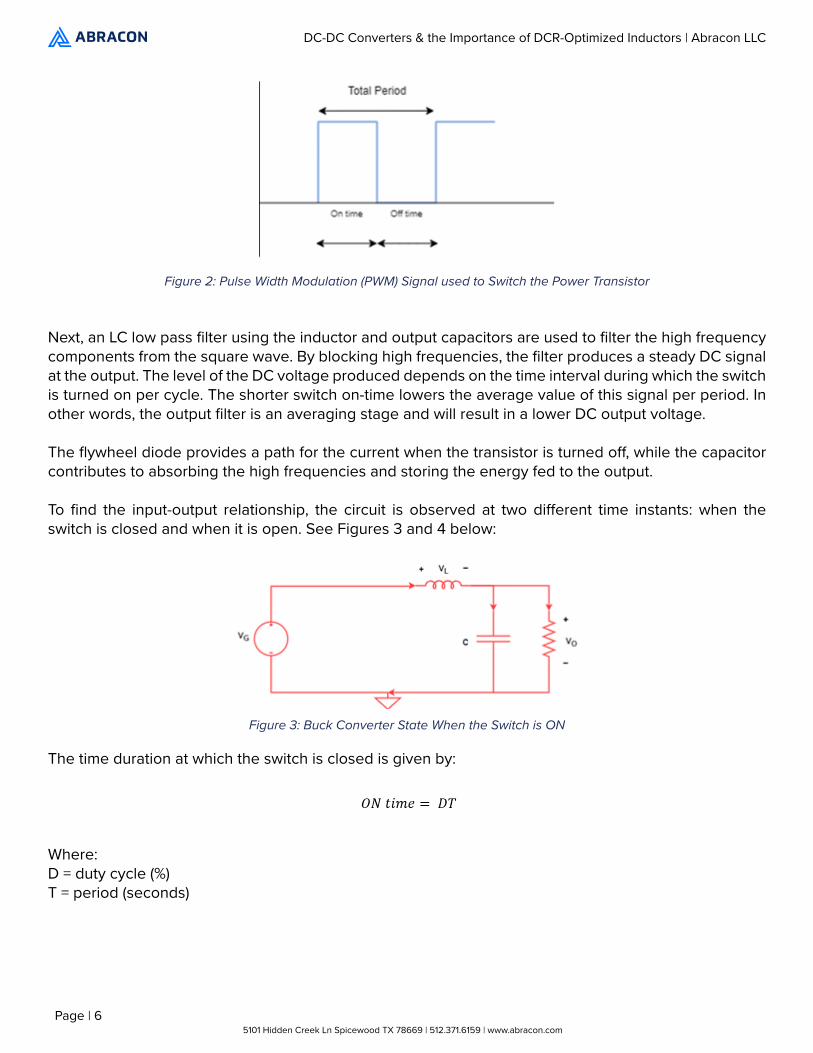
DC-DC converters also offer controllability. The output voltage is controlled using a Pulse Width Modulation (PWM) signal that is fed to the power transistor. Shown in Figure 2, a PWM signal is a periodic square wave in which the width of the square pulses (on time) is modified to control the average delivered power. By adjusting the frequency and the duration when the switch is closed, the output can be set at the desired level, and overall converter efficiency can increase.
One example of an application that uses a DC-DC converter is the voltage regulator module (VRM) found on motherboard designs. The VRM uses the converters to provide adequate voltage levels to different components of the system. For example, microprocessor units require low voltages, so buck converters are utilized in this case to decrease the voltage from the power supply level down to the level required by the microprocessor. [1]
Key Terms
Input-Out RelationshipThe input-output relationship is a mathematical equation that relates the output voltage of the converter to the input voltage. This equation is essential since it allows the designers to calculate the required duty cycle (D) for a given input and output voltage specification.
Referring to Figure 2, duty cycle (D) is the percentage of time during which the switch is on relative to the total period, which is calculated by the following equation:
DC-DC Converters & the Importance of DCR-Optimized Inductors | Abracon LLC
5101 Hidden Creek Ln Spicewood TX 78669 | 512.371.6159 | www.abracon.comPage | 4
Volt-Second BalanceThere are two concepts that are needed to analyze any of the converters: volt-second balance and charge balance. The two principles ensure steady-state operation of the converter. However, only volt-second balance will be discussed in this paper since the equation sufficiently derives the input-output relationship for each converter.
Volt-second balance guarantees that the initial current of an inductor at the beginning of each switching period is equal to the current stored at the end of the same period. (There is no accumulation or reduction of stored electrical energy in the inductor). The same applies for the capacitor through charge balance since the initial voltage stored at the start of each period should be equal to the voltage at the end of the period. (There is no accumulation or reduction of stored electrical energy in the capacitor). By satisfying these conditions, the converter will be functioning in a steady state while avoiding transient state operation.
Given the voltage and current relationship of an inductor, volt-second balance can be characterized using the below formula.
From Faraday’s law of induction:
Where: VL(t) = the voltage across the inductorL = inductancediL (t)/dt = rate of change in current with respect to time
By integrating both sides of the equation above, the equation balances:
To ensure that there is no energy accumulation or reduction, the current of the inductor at the beginning of the period should be equal to the current at the end of the period:
Therefore, the equation can be simplified to the following:
By dividing both sides by the period, the formula becomes Equation 1:
Equation 1
DC-DC Converters & the Importance of DCR-Optimized Inductors | Abracon LLC
5101 Hidden Creek Ln Spicewood TX 78669 | 512.371.6159 | www.abracon.comPage | 5
Where:<VL> = the average voltage of inductorT = time period
Equation 1 indicates that, to satisfy volt-second balance, the average voltage across the inductor over one period should be equal to zero. [2]
Continuous Conduction Mode (CCM)In the following analysis, it will be assumed that all converters are operating in continuous conduction mode (CCM). This means the current will always flow through the inductor without reaching zero amps in a switching cycle. In other words, there is not any instant when both the transistor and the diode are open circuit (no current flow) at the same time. Shown in Figure 5, this ensures that the average current value (IL) is higher than the peak-to-peak ripple current, which is the difference between the maximum and minimum current that flows through the inductor.
By contrast, in discontinuous conduction mode (DCM), the current of the inductor becomes zero for a portion of the switching cycle. This means less average current is delivered to the load, which leads into making the peak-to-peak ripple current higher than the average current. In DCM, since there is more ripple in current, the core losses (power losses in the core of the inductor due to the changing magnetic field) are higher than in the case of CCM, which makes the converter less efficient. Therefore, this paper will concentrate on CCM since this makes it easier to observe the effects of DCR on efficiency while minimizing the impact of core losses.
Topology Analysis
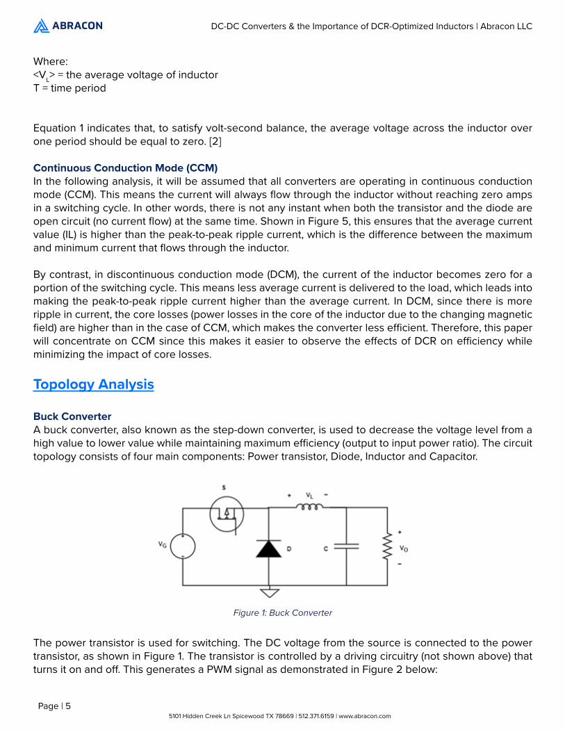
Buck ConverterA buck converter, also known as the step-down converter, is used to decrease the voltage level from a high value to lower value while maintaining maximum efficiency (output to input power ratio). The circuit topology consists of four main components: Power transistor, Diode, Inductor and Capacitor.
The power transistor is used for switching. The DC voltage from the source is connected to the power transistor, as shown in Figure 1. The transistor is controlled by a driving circuitry (not shown above) that turns it on and off. This generates a PWM signal as demonstrated in Figure 2 below:
Figure 1: Buck Converter
DC-DC Converters & the Importance of DCR-Optimized Inductors | Abracon LLC
5101 Hidden Creek Ln Spicewood TX 78669 | 512.371.6159 | www.abracon.comPage | 6
Next, an LC low pass filter using the inductor and output capacitors are used to filter the high frequency components from the square wave. By blocking high frequencies, the filter produces a steady DC signal at the output. The level of the DC voltage produced depends on the time interval during which the switch is turned on per cycle. The shorter switch on-time lowers the average value of this signal per period. In other words, the output filter is an averaging stage and will result in a lower DC output voltage.
The flywheel diode provides a path for the current when the transistor is turned off, while the capacitor contributes to absorbing the high frequencies and storing the energy fed to the output.
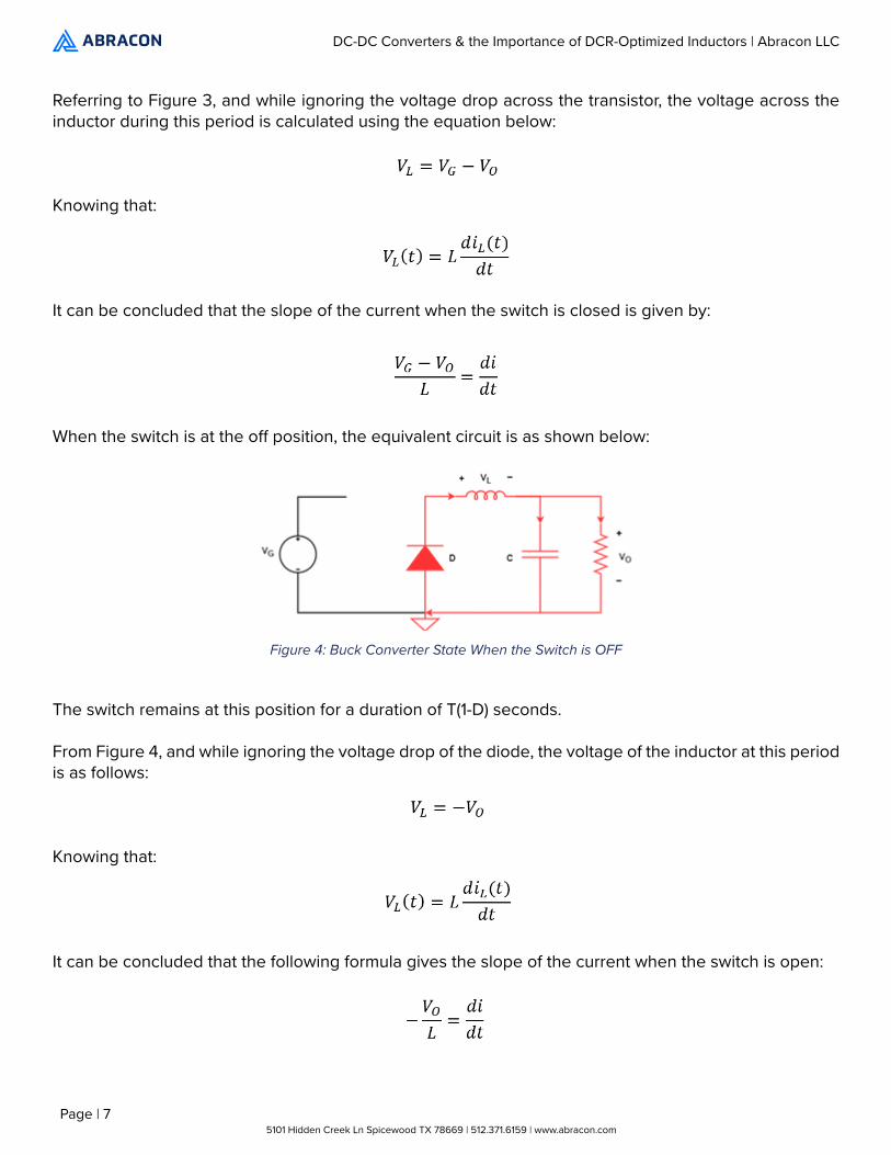
To find the input-output relationship, the circuit is observed at two different time instants: when the switch is closed and when it is open. See Figures 3 and 4 below:
The time duration at which the switch is closed is given by:
Where:D = duty cycle (%)T = period (seconds)
Figure 2: Pulse Width Modulation (PWM) Signal used to Switch the Power Transistor
Figure 3: Buck Converter State When the Switch is ON
DC-DC Converters & the Importance of DCR-Optimized Inductors | Abracon LLC
5101 Hidden Creek Ln Spicewood TX 78669 | 512.371.6159 | www.abracon.comPage | 7
Referring to Figure 3, and while ignoring the voltage drop across the transistor, the voltage across the inductor during this period is calculated using the equation below:
Knowing that:
It can be concluded that the slope of the current when the switch is closed is given by:
When the switch is at the off position, the equivalent circuit is as shown below:
The switch remains at this position for a duration of T(1-D) seconds.
From Figure 4, and while ignoring the voltage drop of the diode, the voltage of the inductor at this period is as follows:
Knowing that:
It can be concluded that the following formula gives the slope of the current when the switch is open:
Figure 4: Buck Converter State When the Switch is OFF
DC-DC Converters & the Importance of DCR-Optimized Inductors | Abracon LLC
5101 Hidden Creek Ln Spicewood TX 78669 | 512.371.6159 | www.abracon.comPage | 8
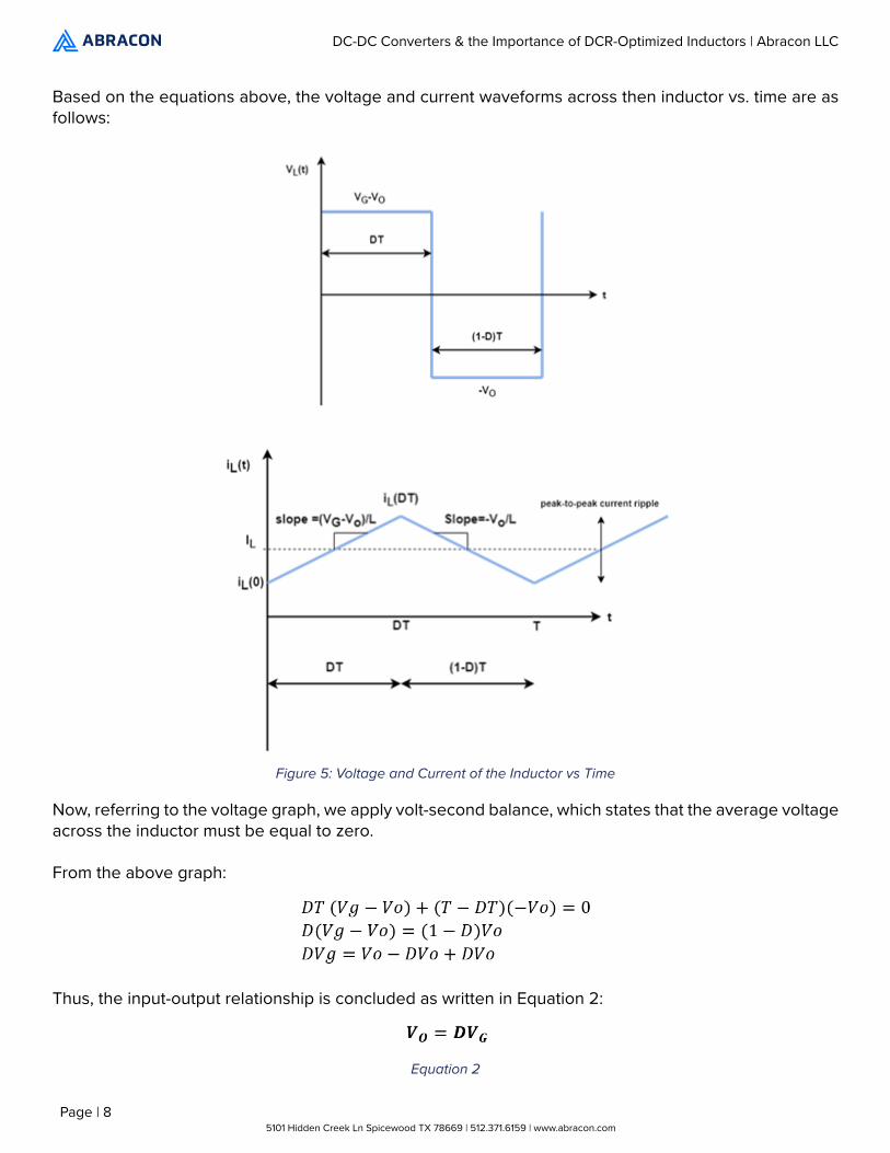
Based on the equations above, the voltage and current waveforms across then inductor vs. time are as follows:
Now, referring to the voltage graph, we apply volt-second balance, which states that the average voltage across the inductor must be equal to zero.
From the above graph:
Thus, the input-output relationship is concluded as written in Equation 2:
Figure 5: Voltage and Current of the Inductor vs Time
Equation 2
DC-DC Converters & the Importance of DCR-Optimized Inductors | Abracon LLC
5101 Hidden Creek Ln Spicewood TX 78669 | 512.371.6159 | www.abracon.comPage | 9
This equation shows that the output voltage is lower since it is a percentage of the input voltage as D ranges between 0 to 1.
The previous analysis was performed while assuming that all components of the circuit are ideal. In real world, this is not the case because all components have power losses through the parasitic elements associated with them. For the scope of this article, only the inductor’s parasitic resistance will be considered.
The parasitic series resistance of the inductor (RL), also known as DCR, has an impact on the output voltage. This can be illustrated by modeling this resistance in series with the inductor and performing the same analysis again.
The input-output relationship can be derived as follows:
At on-state (0<t<DT):
At off-state (DT<t<T):
From volt-second balance, we find:
By simplifying the following:
Given that:
The average current through the inductor is approximately equal to the output current.
Therefore:
Where:
R = load resistance
DC-DC Converters & the Importance of DCR-Optimized Inductors | Abracon LLC
5101 Hidden Creek Ln Spicewood TX 78669 | 512.371.6159 | www.abracon.comPage | 10
Hence:
Thus:
Which can be written as shown in Equation 3:
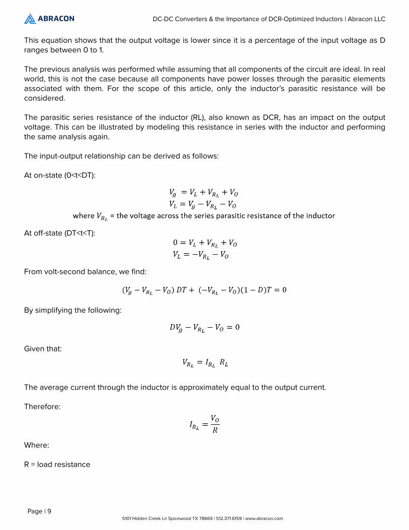
Figure 6 above shows the plots of Equation 3 with the normalized voltage (gain) on the y-axis vs. the duty cycle on the x-axis at different RL/R ratios. When the value of RL is zero, the graph reflects the ideal behavior predicted by Equation 2 with the blue line. For a given load R, as the value of RL increases, the slope of the line changes. This decreases the normalized voltage (gain) value for a given duty cycle, as shown in the green and red lines. [3]
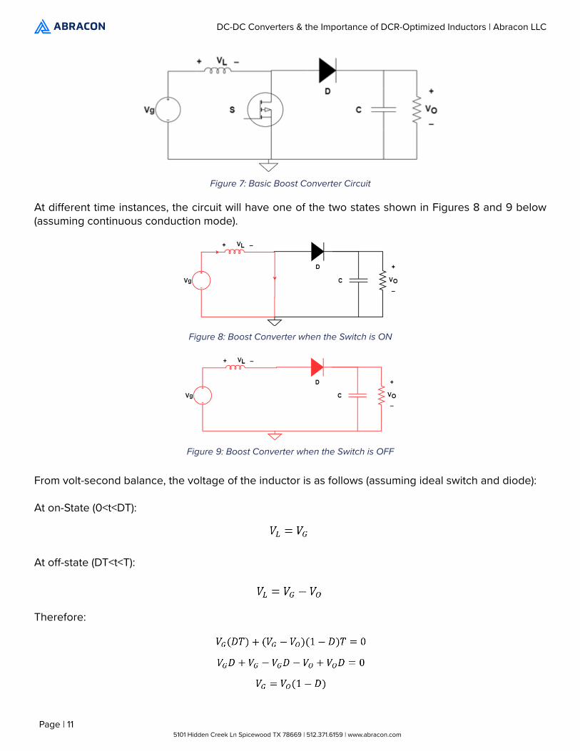
Boost ConverterA boost converter is used to increase the voltage from a low DC level to a higher level. The same analysis discussed in the “Buck Converter” section can be applied to the boost converter topology, as illustrated below:
Equation 3
Figure 6: Normalized Voltage (Gain) vs Duty Cycle [3]
DC-DC Converters & the Importance of DCR-Optimized Inductors | Abracon LLC
5101 Hidden Creek Ln Spicewood TX 78669 | 512.371.6159 | www.abracon.comPage | 11
At different time instances, the circuit will have one of the two states shown in Figures 8 and 9 below (assuming continuous conduction mode).
From volt-second balance, the voltage of the inductor is as follows (assuming ideal switch and diode):
At on-State (0<t<DT):
At off-state (DT<t<T):
Therefore:
Figure 7: Basic Boost Converter Circuit
Figure 8: Boost Converter when the Switch is ON
Figure 9: Boost Converter when the Switch is OFF
DC-DC Converters & the Importance of DCR-Optimized Inductors | Abracon LLC
5101 Hidden Creek Ln Spicewood TX 78669 | 512.371.6159 | www.abracon.comPage | 12
As a result, Equation 4 is shown as the following:
From Equation 4 above, the output voltage can be boosted higher than the input voltage since the term (1-D) is between 0 and 1.
If the non-ideality of the inductor is considered, a parasitic resistance that reflects the DCR would be modeled in series with it. By including it in the circuit and going through the same derivation again, the input-output relationship can be determined as the following equation:
Where:RL = resistance of the inductor R = load resistance
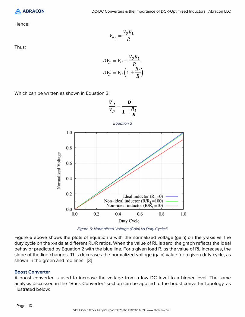
Figure 10, shown above, illustrates the normalized voltage (gain) versus the duty cycle using Equation 5. The curve with RL/R=0 represents the ideal relationship of Equation 5. However, when non-idealities are considered, the gain becomes much lower at a higher duty cycle. The higher the inductor’s DCR, the more reduction on the overall gain. [2]
Buck-Boost ConverterA buck-boost converter is a hybrid between the buck and the boost converter that allows the output voltage to be higher or lower than the input voltage, depending on the duty cycle.
Equation 4
Equation 5
Figure 10: Voltage Gain vs Duty Cycle [5]
DC-DC Converters & the Importance of DCR-Optimized Inductors | Abracon LLC
5101 Hidden Creek Ln Spicewood TX 78669 | 512.371.6159 | www.abracon.comPage | 13
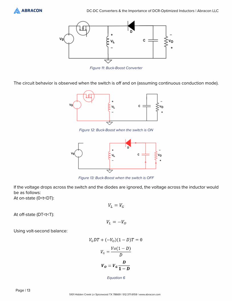
The circuit behavior is observed when the switch is off and on (assuming continuous conduction mode).
If the voltage drops across the switch and the diodes are ignored, the voltage across the inductor would be as follows: At on-state (0<t<DT):
At off-state (DT<t<T):
Using volt-second balance:
Figure 11: Buck-Boost Converter
Figure 12: Buck-Boost when the switch is ON
Figure 13: Buck-Boost when the switch is OFF
Equation 6
DC-DC Converters & the Importance of DCR-Optimized Inductors | Abracon LLC
5101 Hidden Creek Ln Spicewood TX 78669 | 512.371.6159 | www.abracon.comPage | 14
From the equation above, if the duty cycle (D) is less than 0.5, then the converter will operate in the buck mode, meaning the output voltage is less than the input. While, if the duty cycle is more than 0.5, then the converter will operate in boost mode since the output voltage is higher than the input.
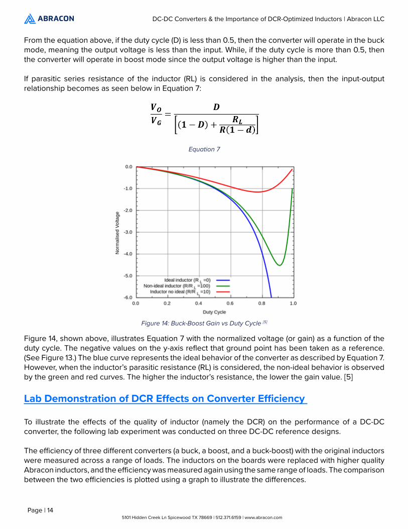
If parasitic series resistance of the inductor (RL) is considered in the analysis, then the input-output relationship becomes as seen below in Equation 7:
Figure 14, shown above, illustrates Equation 7 with the normalized voltage (or gain) as a function of the duty cycle. The negative values on the y-axis reflect that ground point has been taken as a reference. (See Figure 13.) The blue curve represents the ideal behavior of the converter as described by Equation 7. However, when the inductor’s parasitic resistance (RL) is considered, the non-ideal behavior is observed by the green and red curves. The higher the inductor’s resistance, the lower the gain value. [5]
Lab Demonstration of DCR Effects on Converter Efficiency
To illustrate the effects of the quality of inductor (namely the DCR) on the performance of a DC-DC converter, the following lab experiment was conducted on three DC-DC reference designs.
The efficiency of three different converters (a buck, a boost, and a buck-boost) with the original inductors were measured across a range of loads. The inductors on the boards were replaced with higher quality Abracon inductors, and the efficiency was measured again using the same range of loads. The comparison between the two efficiencies is plotted using a graph to illustrate the differences.
Equation 7
Figure 14: Buck-Boost Gain vs Duty Cycle [5]
DC-DC Converters & the Importance of DCR-Optimized Inductors | Abracon LLC
5101 Hidden Creek Ln Spicewood TX 78669 | 512.371.6159 | www.abracon.comPage | 15
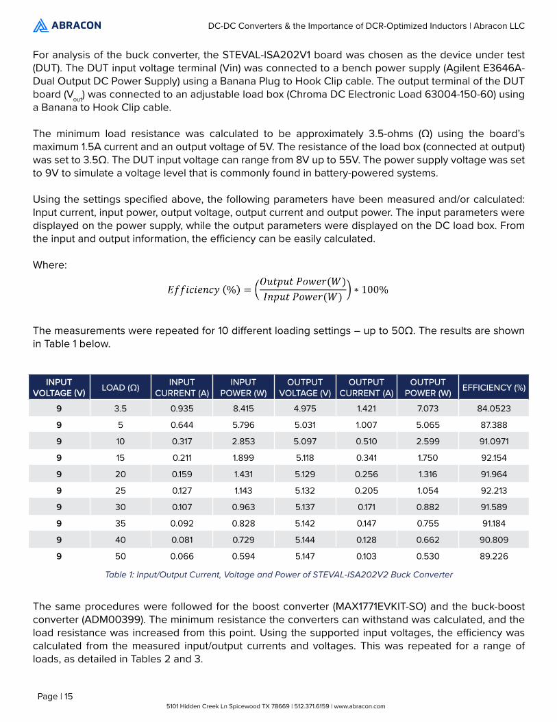
For analysis of the buck converter, the STEVAL-ISA202V1 board was chosen as the device under test (DUT). The DUT input voltage terminal (Vin) was connected to a bench power supply (Agilent E3646A- Dual Output DC Power Supply) using a Banana Plug to Hook Clip cable. The output terminal of the DUT board (Vout) was connected to an adjustable load box (Chroma DC Electronic Load 63004-150-60) using a Banana to Hook Clip cable.
The minimum load resistance was calculated to be approximately 3.5-ohms (Ω) using the board’s maximum 1.5A current and an output voltage of 5V. The resistance of the load box (connected at output) was set to 3.5Ω. The DUT input voltage can range from 8V up to 55V. The power supply voltage was set to 9V to simulate a voltage level that is commonly found in battery-powered systems.
Using the settings specified above, the following parameters have been measured and/or calculated: Input current, input power, output voltage, output current and output power. The input parameters were displayed on the power supply, while the output parameters were displayed on the DC load box. From the input and output information, the efficiency can be easily calculated.
Where:
The measurements were repeated for 10 different loading settings – up to 50Ω. The results are shown in Table 1 below.
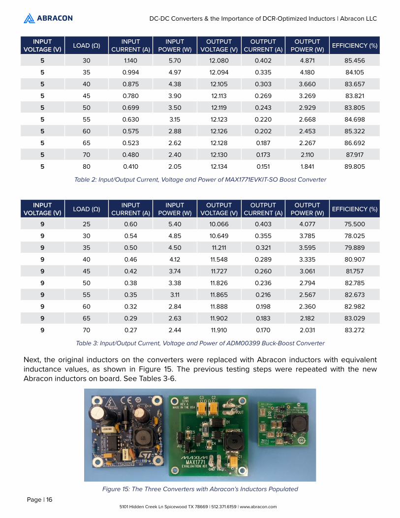
The same procedures were followed for the boost converter (MAX1771EVKIT-SO) and the buck-boost converter (ADM00399). The minimum resistance the converters can withstand was calculated, and the load resistance was increased from this point. Using the supported input voltages, the efficiency was calculated from the measured input/output currents and voltages. This was repeated for a range of loads, as detailed in Tables 2 and 3.
INPUT VOLTAGE (V) LOAD (Ω) INPUT
CURRENT (A) INPUT
POWER (W)OUTPUT
VOLTAGE (V)OUTPUT
CURRENT (A)OUTPUT
POWER (W) EFFICIENCY (%)
9 3.5 0.935 8.415 4.975 1.421 7.073 84.0523
9 5 0.644 5.796 5.031 1.007 5.065 87.388
9 10 0.317 2.853 5.097 0.510 2.599 91.0971
9 15 0.211 1.899 5.118 0.341 1.750 92.154
9 20 0.159 1.431 5.129 0.256 1.316 91.964
9 25 0.127 1.143 5.132 0.205 1.054 92.213
9 30 0.107 0.963 5.137 0.171 0.882 91.589
9 35 0.092 0.828 5.142 0.147 0.755 91.184
9 40 0.081 0.729 5.144 0.128 0.662 90.809
9 50 0.066 0.594 5.147 0.103 0.530 89.226
Table 1: Input/Output Current, Voltage and Power of STEVAL-ISA202V2 Buck Converter
DC-DC Converters & the Importance of DCR-Optimized Inductors | Abracon LLC
5101 Hidden Creek Ln Spicewood TX 78669 | 512.371.6159 | www.abracon.comPage | 16
Next, the original inductors on the converters were replaced with Abracon inductors with equivalent inductance values, as shown in Figure 15. The previous testing steps were repeated with the new Abracon inductors on board. See Tables 3-6.
INPUT VOLTAGE (V) LOAD (Ω) INPUT
CURRENT (A) INPUT
POWER (W)OUTPUT
VOLTAGE (V)OUTPUT
CURRENT (A)OUTPUT
POWER (W) EFFICIENCY (%)
5 30 1.140 5.70 12.080 0.402 4.871 85.456
5 35 0.994 4.97 12.094 0.335 4.180 84.105
5 40 0.875 4.38 12.105 0.303 3.660 83.657
5 45 0.780 3.90 12.113 0.269 3.269 83.821
5 50 0.699 3.50 12.119 0.243 2.929 83.805
5 55 0.630 3.15 12.123 0.220 2.668 84.698
5 60 0.575 2.88 12.126 0.202 2.453 85.322
5 65 0.523 2.62 12.128 0.187 2.267 86.692
5 70 0.480 2.40 12.130 0.173 2.110 87.917
5 80 0.410 2.05 12.134 0.151 1.841 89.805
INPUT VOLTAGE (V) LOAD (Ω) INPUT
CURRENT (A) INPUT
POWER (W)OUTPUT
VOLTAGE (V)OUTPUT
CURRENT (A)OUTPUT
POWER (W) EFFICIENCY (%)
9 25 0.60 5.40 10.066 0.403 4.077 75.500
9 30 0.54 4.85 10.649 0.355 3.785 78.025
9 35 0.50 4.50 11.211 0.321 3.595 79.889
9 40 0.46 4.12 11.548 0.289 3.335 80.907
9 45 0.42 3.74 11.727 0.260 3.061 81.757
9 50 0.38 3.38 11.826 0.236 2.794 82.785
9 55 0.35 3.11 11.865 0.216 2.567 82.673
9 60 0.32 2.84 11.888 0.198 2.360 82.982
9 65 0.29 2.63 11.902 0.183 2.182 83.029
9 70 0.27 2.44 11.910 0.170 2.031 83.272
Table 2: Input/Output Current, Voltage and Power of MAX1771EVKIT-SO Boost Converter
Table 3: Input/Output Current, Voltage and Power of ADM00399 Buck-Boost Converter
Figure 15: The Three Converters with Abracon’s Inductors Populated
DC-DC Converters & the Importance of DCR-Optimized Inductors | Abracon LLC
5101 Hidden Creek Ln Spicewood TX 78669 | 512.371.6159 | www.abracon.comPage | 17
CONVERTER ABRACON’S INDUCTOR USED
ABRACON INDUCTORS DCR (ohms)
ORIGINAL INDUCTOR DCR (ohms)
STEVAL-ISA202V1 (BUCK) ASPI-1205S-121M-T 0.170 0.200
MAX1771EVKIT-SO(BOOST) ASPI-1205S-220M-T 0.036 0.044
ADM00399(Buck-Boost) ASPI-1205S-470M-T 0.075 0.128
INPUT VOLTAGE (V) LOAD (Ω) INPUT
CURRENT (A) INPUT
POWER (W)OUTPUT
VOLTAGE (V)OUTPUT
CURRENT (A)OUTPUT
POWER (W) EFFICIENCY (%)
9 3.5 0.927 8.343 4.983 1.424 7.101 85.113
9 5 0.641 5.769 5.038 1.008 5.077 88.005
9 10 0.316 2.844 5.099 0.510 2.601 91.456
9 15 0.211 1.899 5.119 0.341 1.750 92.154
9 20 0.158 1.422 5.129 0.256 1.317 92.616
9 25 0.128 1.152 5.135 0.205 1.057 91.753
9 30 0.107 0.963 5.138 0.171 0.881 91.485
9 35 0.092 0.828 5.141 0.147 0.755 91.184
9 40 0.081 0.729 5.143 0.129 0.663 90.947
9 50 0.066 0.594 5.146 0.103 0.530 89.226
INPUT VOLTAGE (V) LOAD (Ω) INPUT
CURRENT (A) INPUT
POWER (W)OUTPUT
VOLTAGE (V)OUTPUT
CURRENT (A)OUTPUT
POWER (W) EFFICIENCY (%)
5 30 1.140 5.70 12.087 0.403 4.875 85.526
5 35 0.990 4.95 12.102 0.346 4.190 84.646
5 40 0.870 4.35 12.114 0.303 3.670 84.369
5 45 0.775 3.88 12.122 0.270 3.281 84.671
5 50 0.687 3.44 12.128 0.242 2.940 85.590
5 55 0.615 3.08 12.132 0.221 2.680 87.154
5 60 0.552 2.76 12.135 0.202 2.454 88.913
5 65 0.497 2.49 12.138 0.186 2.260 90.946
5 70 0.455 2.28 12.140 0.173 2.110 92.747
5 80 0.385 1.93 12.144 0.152 1.845 95.844
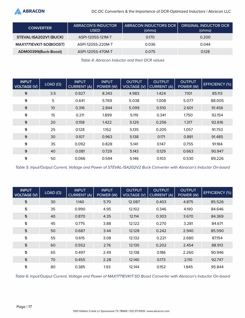
Table 4: Abracon Inductor and their DCR values
Table 5: Input/Output Current, Voltage and Power of STEVAL-ISA202V2 Buck Converter with Abracon’s Inductor On-board
Table 6: Input/Output Current, Voltage and Power of MAX1771EVKIT-SO Boost Converter with Abracon’s Inductor On-board
DC-DC Converters & the Importance of DCR-Optimized Inductors | Abracon LLC
5101 Hidden Creek Ln Spicewood TX 78669 | 512.371.6159 | www.abracon.comPage | 18
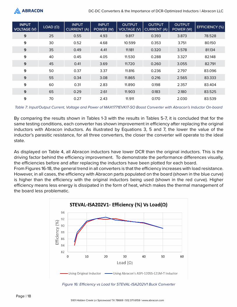
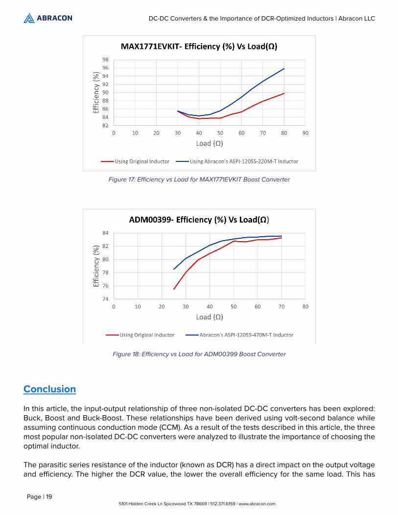
By comparing the results shown in Tables 1-3 with the results in Tables 5-7, it is concluded that for the same testing conditions, each converter has shown improvement in efficiency after replacing the original inductors with Abracon inductors. As illustrated by Equations 3, 5 and 7, the lower the value of the inductor’s parasitic resistance, for all three converters, the closer the converter will operate to the ideal state.
As displayed on Table 4, all Abracon inductors have lower DCR than the original inductors. This is the driving factor behind the efficiency improvement. To demonstrate the performance differences visually, the efficiencies before and after replacing the inductors have been plotted for each board.From Figures 16-18, the general trend in all converters is that the efficiency increases with load resistance. However, in all cases, the efficiency with Abracon parts populated on the board (shown in the blue curve) is higher than the efficiency with the original inductors being used (shown in the red curve). Higher efficiency means less energy is dissipated in the form of heat, which makes the thermal management of the board less problematic.
INPUT VOLTAGE (V) LOAD (Ω) INPUT
CURRENT (A) INPUT
POWER (W)OUTPUT
VOLTAGE (V)OUTPUT
CURRENT (A)OUTPUT
POWER (W) EFFICIENCY (%)
9 25 0.55 4.93 9.817 0.393 3.873 78.528
9 30 0.52 4.68 10.599 0.353 3.751 80.150
9 35 0.49 4.41 11.181 0.320 3.578 81.134
9 40 0.45 4.05 11.530 0.288 3.327 82.148
9 45 0.41 3.69 11.720 0.260 3.055 82.791
9 50 0.37 3.37 11.816 0.236 2.797 83.096
9 55 0.34 3.08 11.865 0.216 2.565 83.333
9 60 0.31 2.83 11.890 0.198 2.357 83.404
9 65 0.29 2.61 11.903 0.183 2.180 83.525
9 70 0.27 2.43 11.911 0.170 2.030 83.539
Table 7: Input/Output Current, Voltage and Power of MAX1771EVKIT-SO Boost Converter with Abracon’s Inductor On-board
Figure 16: Efficiency vs Load for STEVAL-ISA202V1 Buck Converter
DC-DC Converters & the Importance of DCR-Optimized Inductors | Abracon LLC
5101 Hidden Creek Ln Spicewood TX 78669 | 512.371.6159 | www.abracon.comPage | 19
Conclusion
In this article, the input-output relationship of three non-isolated DC-DC converters has been explored: Buck, Boost and Buck-Boost. These relationships have been derived using volt-second balance while assuming continuous conduction mode (CCM). As a result of the tests described in this article, the three most popular non-isolated DC-DC converters were analyzed to illustrate the importance of choosing the optimal inductor.
The parasitic series resistance of the inductor (known as DCR) has a direct impact on the output voltage and efficiency. The higher the DCR value, the lower the overall efficiency for the same load. This has
Figure 17: Efficiency vs Load for MAX1771EVKIT Boost Converter
Figure 18: Efficiency vs Load for ADM00399 Boost Converter

DC-DC Converters & the Importance of DCR-Optimized Inductors | Abracon LLC
5101 Hidden Creek Ln Spicewood TX 78669 | 512.371.6159 | www.abracon.comPage | 20
been validated both mathematically and experimentally.
The higher quality, DCR-optimized Abracon inductors yielded higher efficiencies when compared to the original inductors used in the tested converters. This resulted in improved circuit power loss and associated generated heat. In more complex designs, scaling this by ‘n’ number of DC-DC converters in the system has significant impact on thermal design considerations.
Furthermore, higher efficiency inductors help reduce output ripple current. Reducing output ripple current can help minimize the heat generated by the output capacitors’ ESR. This allows system designers to create complex power solutions utilizing miniature components requiring less board space.
Author Information:Ahmed Alamin
Associate Engineer – Inductors & ConnectivityAbracon, LLC
DC-DC Converters & the Importance of DCR-Optimized Inductors | Abracon LLC
5101 Hidden Creek Ln Spicewood TX 78669 | 512.371.6159 | www.abracon.comPage | 21
References
[1] D. Knight, “Buck Converters and Their Cool Applications - Technical Articles,” All About Circuits, 24-Nov-2015. [Online]. Available: https://www.allaboutcircuits.com/technical-articles/buck-converters-and-their-cool-applications/.
[2] R. W. Erickson, “Introduction to Power Electronics,” University of Colorado Boulder, 26-Aug-2015. [Online]. Available: https://ecee.colorado.edu/. [Accessed: 16-Mar-2021].
[3] “Buck converter,” Wikipedia, 11-Mar-2021. [Online]. Available: https://en.wikipedia.org/wiki/Buck_converter. [Accessed: 16-Mar-2021].
[4] M. Garg, M. Pathak, and Y. Hote, “Effect of Non-Idealities on the Design and Performance of a DC-DC Buck Converter ,” Journal of Power Electronics, vol. 16, no. 3, pp. 832–839, May 2016.
[5] “Buck–boost converter,” Wikipedia, 21-Sep-2020. [Online]. Available: https://en.wikipedia.org/wiki/Buck%E2%80%93boost_converter. [Accessed: 16-Mar-2021].


![Series Inductors - IHLP - Vishay · Inductors - IHLP ® Series For Commercial Applications features Model Inductance Range** dcR Max Rated current* dimensions in Inches [mm] IHLP-1212aB-11](https://img.pdfslide.us/doc/110x75/5c65a99c09d3f2a86e8cf3cd/series-inductors-ihlp-inductors-ihlp-series-for-commercial-applications.jpg)